WO2025079375A1 - 反射型マスクブランク、反射型マスク、反射型マスクブランクの製造方法、及び反射型マスクの製造方法 - Google Patents
反射型マスクブランク、反射型マスク、反射型マスクブランクの製造方法、及び反射型マスクの製造方法 Download PDFInfo
- Publication number
- WO2025079375A1 WO2025079375A1 PCT/JP2024/032153 JP2024032153W WO2025079375A1 WO 2025079375 A1 WO2025079375 A1 WO 2025079375A1 JP 2024032153 W JP2024032153 W JP 2024032153W WO 2025079375 A1 WO2025079375 A1 WO 2025079375A1
- Authority
- WO
- WIPO (PCT)
- Prior art keywords
- film
- reflective mask
- gas
- compound
- absorbing
- Prior art date
- Legal status (The legal status is an assumption and is not a legal conclusion. Google has not performed a legal analysis and makes no representation as to the accuracy of the status listed.)
- Pending
Links
Images


Classifications
-
- G—PHYSICS
- G03—PHOTOGRAPHY; CINEMATOGRAPHY; ANALOGOUS TECHNIQUES USING WAVES OTHER THAN OPTICAL WAVES; ELECTROGRAPHY; HOLOGRAPHY
- G03F—PHOTOMECHANICAL PRODUCTION OF TEXTURED OR PATTERNED SURFACES, e.g. FOR PRINTING, FOR PROCESSING OF SEMICONDUCTOR DEVICES; MATERIALS THEREFOR; ORIGINALS THEREFOR; APPARATUS SPECIALLY ADAPTED THEREFOR
- G03F1/00—Originals for photomechanical production of textured or patterned surfaces, e.g., masks, photo-masks, reticles; Mask blanks or pellicles therefor; Containers specially adapted therefor; Preparation thereof
- G03F1/22—Masks or mask blanks for imaging by radiation of 100nm or shorter wavelength, e.g. X-ray masks, extreme ultraviolet [EUV] masks; Preparation thereof
- G03F1/24—Reflection masks; Preparation thereof
-
- G—PHYSICS
- G03—PHOTOGRAPHY; CINEMATOGRAPHY; ANALOGOUS TECHNIQUES USING WAVES OTHER THAN OPTICAL WAVES; ELECTROGRAPHY; HOLOGRAPHY
- G03F—PHOTOMECHANICAL PRODUCTION OF TEXTURED OR PATTERNED SURFACES, e.g. FOR PRINTING, FOR PROCESSING OF SEMICONDUCTOR DEVICES; MATERIALS THEREFOR; ORIGINALS THEREFOR; APPARATUS SPECIALLY ADAPTED THEREFOR
- G03F1/00—Originals for photomechanical production of textured or patterned surfaces, e.g., masks, photo-masks, reticles; Mask blanks or pellicles therefor; Containers specially adapted therefor; Preparation thereof
- G03F1/54—Absorbers, e.g. of opaque materials
Definitions
- EUV extreme ultraviolet
- EUV includes soft X-rays and vacuum ultraviolet light, and specifically refers to light with a wavelength of approximately 0.2 nm to 100 nm. At present, EUV with a wavelength of approximately 13.5 nm is mainly being considered.
- the reflective mask blank described in Patent Document 1 has a protective film made of a Ru compound containing Ru and X (X is at least one selected from Nb and Zr).
- This protective film has an oxide layer mainly composed of X on the surface opposite the substrate of the protective film for the purpose of improving resistance to ozone water and improving resistance to etching gas (containing 70% or more oxygen and including chlorine-based gas).
- the protective film is made of a Ru-based material
- the phase shift film is made of a Ta-based material.
- a diffusion prevention layer is formed on the surface of the protective film (the surface in contact with the phase shift film).
- the diffusion prevention layer contains Ru and O, and inhibits interdiffusion between the protective film and the phase shift film.
- FIG. 1 is a cross-sectional view showing a reflective mask blank according to one embodiment.
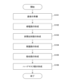
- FIG. 2 is a flowchart showing a method for manufacturing a reflective mask blank according to an embodiment.
- FIG. 3 is a cross-sectional view showing a reflective mask according to an embodiment.
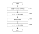
- FIG. 4 is a flowchart showing a method for manufacturing a reflective mask according to an embodiment.
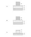
- 5A is a cross-sectional view showing an example of S201
- FIG. 5B is a cross-sectional view showing an example of S202
- FIG. 5C is a cross-sectional view showing an example of S203.
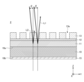
- FIG. 6 is a cross-sectional view showing an example of EUV light reflected by the reflective mask of FIG.
- FIG. 6 is a cross-sectional view showing an example of EUV light reflected by the reflective mask of FIG. FIG.
- FIG. 7 is a diagram showing a TEM image of the reflective mask blank according to Example 1 and the distribution of each element measured by TEM-EDX.
- FIG. 8 is a diagram showing a TEM image of the reflective mask blank according to Example 5 and the distribution of each element measured by TEM-EDX.
- the X-axis direction, the Y-axis direction, and the Z-axis direction are mutually orthogonal.
- the Z-axis direction is perpendicular to the first major surface 10a of the substrate 10.
- the X-axis direction is perpendicular to the incidence surface of the EUV light (the surface including the incident light beam and the reflected light beam). As shown in FIG. 6, the incident light beam is inclined toward the Y-axis positive direction as it moves toward the Z-axis negative direction, and the reflected light beam is inclined toward the Y-axis positive direction as it moves toward the Z-axis positive direction.
- the reflective mask blank 1 may have a conductive film 15 on the opposite side to the multilayer reflective film 11 with respect to the substrate 10. That is, the reflective mask blank 1 may have the conductive film 15, the substrate 10, the multilayer reflective film 11, the protective film 12, the absorbing film 13, and the hard mask film 14, in this order.
- the conductive film 15 is formed on the second main surface 10b of the substrate 10.
- the second main surface 10b is the surface facing opposite to the first main surface 10a.
- the conductive film 15 is used, for example, to attach the reflective mask 2 to an electrostatic chuck of an exposure device.
- the reflective mask blank 1 may further have a functional film not shown in FIG. 1.
- the reflective mask blank 1 may have a diffusion barrier film (not shown) between the multilayer reflective film 11 and the protective film 12.
- the diffusion barrier film suppresses the diffusion of metal elements contained in the protective film 12 into the multilayer reflective film 11.
- steps S101 to S106 is not limited to the order shown in FIG. 2.
- the order of step S102 and steps S103 to S106 may be reversed.
- the method for manufacturing the reflective mask blank 1 does not have to include all of steps S101 to S106.
- the method for manufacturing the reflective mask blank 1 may further include a step of forming a functional film not shown in FIG. 2.
- the reflective mask 2 is produced, for example, using the reflective mask blank 1 shown in FIG. 1, and includes an opening pattern 13a in an absorbing film 13.
- the opening pattern 13a in the absorbing film 13 is transferred to a target substrate such as a semiconductor substrate. Transferring includes reducing and transferring. Note that the hard mask film 14 shown in FIG. 1 is not included in the reflective mask 2.
- a method for manufacturing a reflective mask 2 has steps S201 to S204 shown in Figure 4.
- a reflective mask blank 1 is prepared as shown in Figure 5 (A).
- the reflective mask blank 1 includes a resist film 16 as shown in Figure 5 (A).
- the resist film 16 is formed on a hard mask film 14.
- An opening pattern to be transferred to the absorbing film 13 is formed in the resist film 16.
- the first etching gas is selected according to the combination of the material of the hard mask film 14 and the material of the absorbing film 13, and includes, but is not limited to, a chlorine-based gas and an oxygen-based gas.
- the chlorine-based gas includes at least one selected from, for example, Cl2 gas, SiCl4 gas, CHCl3 gas, CCl4 gas, and BCl3 gas.
- the oxygen-based gas includes at least one selected from, for example, O2 gas and O3 gas.
- the first etching gas may include an inert gas in addition to the chlorine-based gas and the oxygen-based gas.
- the inert gas includes at least one selected from, for example, N2 gas, He gas, and Ar gas.
- the first etching gas is preferably a plasma gas.
- the quality assurance area of the first main surface 10a preferably has a root-mean-square roughness (Rq) of 0.15 nm or less and a flatness of 100 nm or less. In addition, it is preferable that the quality assurance area of the first main surface 10a does not have any defects that cause phase defects.
- each layer constituting the multilayer reflective film 11 and the number of repeat units of the layers can be appropriately selected depending on the material of each layer and the reflectivity to EUV light.
- the multilayer reflective film 11 is a Mo/Si multilayer reflective film, in order to achieve a reflectivity of 60% or more for EUV light with an incident angle ⁇ (see FIG. 6) of 6°, Mo layers with a thickness of 2.3 ⁇ 0.1 nm and Si layers with a thickness of 4.5 ⁇ 0.1 nm can be stacked so that the number of repeat units is 30 or more and 60 or less. It is preferable that the multilayer reflective film 11 has a reflectivity of 60% or more for EUV light with an incident angle ⁇ of 6°. The reflectivity is more preferably 65% or more.
- the protective film 12 When the protective film 12 contains Ru, it may exhibit crystallinity. If the protective film 12 crystallizes, the absorbing film 13 may inherit the crystal structure of the protective film 12, causing the absorbing film 13 to crystallize. As a result, the opening pattern 13a is formed along the crystal grain boundaries of the absorbing film 13, and the opening pattern 13a becomes rough.
- the protective film 12 of this embodiment contains a Ru compound, and the Ru compound contains Ru, Si, and O.
- Si is more easily oxidized than Ru, and the O concentration in the Ru compound can be increased. O suppresses the crystallization of Ru. Therefore, the crystallization of the protective film 12 can be suppressed, and the crystallization of the absorbing film 13 can be suppressed.
- the Ru compound constituting the protective film 12 preferably has an average O concentration of less than 12.6 at%. If the average O concentration is less than 12.6 at%, the O concentration is not too high and the generation of defects including SiO can be suppressed. The generation of defects including SiO causes surface roughness of the protective film 12.
- the average O concentration is more preferably 10.0 at% or less, and even more preferably 8.0 at% or less.
- the RuSiO film can also be formed by reactive sputtering.
- the element ratio of Ru and Si can be adjusted by controlling the output density of each of the Ru target and the Si target.
- the O concentration can be adjusted by controlling the volume ratio of O2 gas in the sputtering gas ( O2 /(Ar+ O2 )).
- the O concentration is constant, for example, regardless of the depth from the surface of the RuSiO film.
- the O concentration can be made to slope in the depth direction, or only the outermost layer can be oxidized.
- the protective film 12 is a film consisting of a single layer, but it may be a multi-layer film having a lower layer and an upper layer.
- the lower layer of the protective film 12 is a layer formed in contact with the uppermost surface of the multilayer reflective film 11.
- the upper layer of the protective film 12 is in contact with the lowermost surface of the absorbing film 13.
- the thickness of the protective film 12 is preferably 1.0 nm to 7.0 nm, more preferably 2.0 nm to 6.5 nm, and even more preferably 2.5 nm to 6.5 nm. If the thickness of the protective film 12 is 1.0 nm or more, the etching resistance is good. Furthermore, if the thickness of the protective film 12 is 7.0 nm or less, the reflectance to EUV light is good.
- the density of the protective film 12 is preferably 10.0 g/cm 3 to 14.0 g/cm 3. If the density of the protective film 12 is 10.0 g/cm 3 or more, the etching resistance is good. Furthermore, if the density of the protective film 12 is 14.0 g/cm 3 or less, the decrease in reflectance for EUV light can be suppressed.
- the upper surface of the protective film 12, i.e., the surface of the protective film 12 on which the absorbing film 13 is formed, preferably has a root-mean-square roughness Rq of 0.20 nm or less, more preferably 0.17 nm or less. If the root-mean-square roughness Rq is 0.20 nm or less, the absorbing film 13 and the like can be formed smoothly on the protective film 12. In addition, scattering of EUV light can be suppressed, and the reflectance for EUV light can be improved.
- the root-mean-square roughness Rq is preferably 0.05 nm or more.
- the method for forming the protective film 12 is, for example, DC sputtering, magnetron sputtering, ion beam sputtering, etc.
- an example of the film formation conditions is as follows. ⁇ RuSi film formation conditions> Target: Ru target and Si target, Sputtering gas: Ar gas, Gas pressure: 1.0 ⁇ 10 ⁇ 2 Pa to 1.0 ⁇ 10 0 Pa, Target power density: 1.0 W/cm 2 to 8.5 W/cm 2 , Film formation rate: 0.020 nm/sec to 1.000 nm/sec, Film thickness: 1 nm to 10 nm.
- ⁇ RuSi film oxidation conditions (plasma treatment conditions)> Flow rate of O2 gas: 200 sccm to 3000 sccm Ar gas flow rate: 100 sccm to 6000 sccm Proportion of O2 gas in the mixed gas of O2 gas and Ar gas: 0% by volume to 90% by volume Power supply frequency for plasma generation: 10MHz to 60MHz Power for plasma generation: 50W to 600W Processing time: 2 sec to 120 sec Treatment temperature: 80°C to 350°C Treatment pressure: 50 Pa to 1200 Pa.
- the absorbing film 13 absorbs EUV light.
- the absorbing film 13 is a film in which an opening pattern 13a is to be formed.
- the opening pattern 13a is not formed in the manufacturing process of the reflective mask blank 1, but is formed in the manufacturing process of the reflective mask 2.
- the absorbing film 13 may not only absorb EUV light, but may also shift the phase of the EUV light. In other words, the absorbing film 13 may be a phase shift film.
- the phase shift film shifts the phase of the second EUV light L2 relative to the first EUV light L1 shown in FIG. 6.
- the first EUV light L1 is light that passes through the opening pattern 13a without passing through the absorbing film 13, is reflected by the multilayer reflective film 11, and passes through the opening pattern 13a without passing through the absorbing film 13 again.
- the second EUV light L2 is light that passes through the absorbing film 13 while being absorbed by the absorbing film 13, is reflected by the multilayer reflective film 11, and passes through the absorbing film 13 while being absorbed by the absorbing film 13 again.
- the phase difference ( ⁇ 0) between the first EUV light L1 and the second EUV light L2 is, for example, 170° to 250°.
- the phase of the first EUV light L1 may be ahead of or behind the phase of the second EUV light L2.
- the absorbing film 13 uses the interference between the first EUV light L1 and the second EUV light L2 to improve the contrast of the transferred image.
- the transferred image is an image of the opening pattern 13a of the absorbing film 13 transferred onto the target substrate.
- the so-called projection effect occurs.
- the shadowing effect is caused by the fact that the incident angle ⁇ of the EUV light is not 0° (for example, 6°), and therefore an area where the sidewall blocks the EUV light occurs near the sidewall of the opening pattern 13a, causing a positional or dimensional shift in the transferred image.
- it is effective to lower the height of the sidewall of the opening pattern 13a, and thin the absorbing film 13.
- the thickness of the absorbing film 13 is, for example, 60 nm or less, and preferably 50 nm or less, in order to reduce the shadowing effect.
- the thickness of the absorbing film 13 is preferably 20 nm or more, and more preferably 30 nm or more, in order to ensure a phase difference between the first EUV light L1 and the second EUV light L2.
- the absorbing film 13 In order to reduce the thickness of the absorbing film 13 to reduce the shadowing effect while maintaining the phase difference between the first EUV light L1 and the second EUV light L2, it is effective to reduce the refractive index n of the absorbing film 13. Also, in order to reduce the reflectance for EUV light, it is effective to increase the extinction coefficient k of the absorbing film 13. Thus, the absorbing film 13 is required to have excellent optical properties.
- the absorbing film 13 preferably contains at least one metal element selected from Cr, Ta, Nb, Ir, Pt, Pd, Au, and Ru. These metal elements have a relatively small refractive index, so the thickness of the absorbing film 13 can be reduced while maintaining the phase difference.
- the absorbing film 13 preferably contains a compound of a metal element.
- the compound of a metal element preferably contains at least one element selected from O, B, C, Si, and N. By adding at least one element selected from O, B, C, Si, and N, it is possible to suppress crystallization while suppressing the deterioration of optical characteristics, and to reduce the roughness of the opening pattern 13a.
- the absorbing film 13 contains a Ta compound. It is more preferable that the Ta compound contains N. This is because the inclusion of N can suppress the crystallization of the Ta compound and prevent surface roughness due to crystallization. It is preferable that the absorbing film 13 contains TaN.
- the absorbing film 13 is a film consisting of a single layer, but it may be a multilayer film having a lower layer and an upper layer.
- the lower layer and upper layer constituting the absorbing film 13 are formed on the protective film 12 in this order.
- the uppermost layer of the absorbing film 13 is the layer farthest from the protective film 12.
- the uppermost layer of the absorbing film 13 preferably contains at least one metal element selected from Cr, Ta, Nb, Ir, Pt, Pd, Au, and Ru, and more preferably contains a compound of the metal element.
- the uppermost layer of the absorbing film 13 more preferably contains a Ta compound.
- the Ta compound is more preferable because it contains N, which suppresses the crystallization of Ta and prevents the crystals from becoming large and the surface roughness from increasing.
- the absorbing film 13 preferably contains TaN.
- the thickness of the absorbing film 13 means the total film thickness of the multilayer film.
- the N atom content of the Ta compound is preferably 10.0 to 35.0 at% in order to increase the etching selectivity, more preferably 10.0 to 25.0 at%, even more preferably 10.5 to 18.0 at%, and particularly preferably 11.0 to 16.0 at%.
- the Ta compound may further contain at least one element selected from hafnium (Hf), silicon (Si), zirconium (Zr), titanium (Ti), germanium (Ge), boron (B), tin (Sn), nickel (Ni), cobalt (Co) and hydrogen (H).
- Hf hafnium
- Si silicon
- Zr zirconium
- Ti titanium
- Ge germanium
- B boron
- Sn tin
- Ni nickel
- Co cobalt
- H hydrogen
- the total content of these elements is preferably 10 at% or less.
- the method for forming the absorbing film 13 is, for example, a DC sputtering method, a magnetron sputtering method, an ion beam sputtering method, etc.
- the nitrogen content of the absorbing film 13 can be controlled by the content of N2 gas in the sputtering gas.
- TaN film formation conditions ⁇ TaN film formation conditions> Target: Ta target, Power density of Ta target: 1.0 W/cm 2 to 8.5 W/cm 2 , Sputtering gas: a mixture of Ar gas and N2 gas, Volume ratio of N2 gas in the sputtering gas ( N2 /(Ar+ N2 )): 0.01 to 0.25, Gas pressure: 1.0 ⁇ 10 ⁇ 2 Pa to 1.0 ⁇ 10 0 Pa, Power density of Ta target: 1.0 W/cm 2 to 8.5 W/cm 2 , Film formation rate: 0.020 nm/sec to 0.060 nm/sec, Film thickness: 20 nm to 60 nm.
- the absorbing film 13 preferably has an extremely low reflectance to EUV light. Specifically, the absorbing film 13 preferably has a reflectance of 2.0% or less to light with a wavelength of 13.5 nm, more preferably 1.0% or less, even more preferably 0.5% or less, and particularly preferably 0.1% or less. The absorbing film 13 has a reflectance of 0.0% or more to light with a wavelength of 13.5 nm.
- the hard mask film 14 is formed on the opposite side of the protective film 12 with respect to the absorbing film 13, and is used to form an opening pattern 13a in the absorbing film 13.
- the hard mask film 14 enables the resist film 16 to be thinned.
- the thickness of the hard mask film 14 is preferably 2 nm or more and 30 nm or less, more preferably 2 nm or more and 25 nm or less, and even more preferably 2 nm or more and 10 nm or less.
- the hard mask film 14 can be formed, for example, by DC sputtering, magnetron sputtering, or ion beam sputtering.
- the conductive film 15 is a film consisting of a single layer, but it may be a multi-layer film having a lower layer and an upper layer.
- the lower layer and upper layer constituting the conductive film 15 are formed on the substrate 10 in this order.
- the uppermost layer of the conductive film 15 is the layer furthest from the substrate 10.
- the uppermost layer of the conductive film 15 preferably contains at least one metal element selected from Cr and Ta, and more preferably contains a compound of the above metal elements.
- the thickness of the conductive film 15 means the total film thickness of the multi-layer film.
- the thickness of the conductive film 15 is preferably 5 nm or more and 500 nm or less, more preferably 10 nm or more and 450 nm or less, and even more preferably 20 nm or more and 400 nm or less.
- the conductive film 15 can be formed, for example, by DC sputtering, magnetron sputtering, or ion beam sputtering.
- a SiO 2 -TiO 2 type glass substrate (6 inch (152 mm) square outer shape, 6.3 mm thick) was prepared.
- This glass substrate had a thermal expansion coefficient of 0.02 ⁇ 10 -7 /°C at 20°C, a Young's modulus of 67 GPa, a Poisson's ratio of 0.17, and a specific rigidity of 3.07 ⁇ 10 7 m 2 /s 2.
- the quality assurance area of the first main surface 10a of the substrate 10 was polished to have a root-mean-square roughness (Rq) of 0.15 nm or less and a flatness of 100 nm or less.
- a 100 nm thick Cr film was formed on the second main surface 10b of the substrate 10 by magnetron sputtering. The sheet resistance of the Cr film was 100 ⁇ / ⁇ .
- a Mo/Si multilayer reflective film was formed as the multilayer reflective film 11.
- the Mo/Si multilayer reflective film was formed by repeating the deposition of a Si layer (film thickness 4.5 nm) and a Mo layer (film thickness 2.3 nm) 40 times using an ion beam sputtering method.
- the total thickness of the Mo/Si multilayer reflective film was 272 nm ((4.5 nm + 2.3 nm) x 40).
- the top layer of the Mo/Si multilayer reflective film was a Si layer.
- the non-crystallinity of the TaN film is "A” indicates that the full width at half maximum of the most intense peak in the 2 ⁇ range of 20° to 50° measured by XRD using CuK ⁇ radiation was 1.0° or more, meaning that crystallization of the TaN film was suppressed.
- the presence or absence of defects containing SiO is "A” indicates that no micro-defects due to defects containing SiO were observed on the surface of the TaN film using SEM
- the presence or absence of defects containing SiO is "B” indicates that micro-defects due to defects containing SiO were observed on the surface of the TaN film using SEM.
- the protective film 12 was a RuSiO film, so crystallization of the TaN film, which is the absorbing film 13, could be suppressed. It has also been confirmed that even when the material of the absorbing film 13 is an Nb-based material or an Ir-based material, if the protective film 12 is a RuSiO film, crystallization of the absorbing film 13 can be suppressed. Also, as shown in Table 1, in Examples 1 to 4, unlike Example 5, the Si concentration of the RuSiO film was less than 37.9 at%, so no micro-defects due to defects containing SiO were observed on the surface of the TaN film using an SEM.
- Figure 7 shows a TEM image of the reflective mask blank of Example 1 and the distribution of each element measured by TEM-EDX.
- Figure 8 shows a TEM image of the reflective mask blank of Example 5 and the distribution of each element measured by TEM-EDX. As shown in Figure 8, defects containing SiO were found at the interface between the RuSiO film and the TaN film in Example 5, but defects containing SiO were not found at the interface between the RuSiO film and the TaN film in Example 1.
Landscapes
- Physics & Mathematics (AREA)
- General Physics & Mathematics (AREA)
- Preparing Plates And Mask In Photomechanical Process (AREA)
- Exposure Of Semiconductors, Excluding Electron Or Ion Beam Exposure (AREA)
Priority Applications (1)
| Application Number | Priority Date | Filing Date | Title |
|---|---|---|---|
| JP2025522220A JPWO2025079375A1 (https=) | 2023-10-10 | 2024-09-09 |
Applications Claiming Priority (2)
| Application Number | Priority Date | Filing Date | Title |
|---|---|---|---|
| JP2023174933 | 2023-10-10 | ||
| JP2023-174933 | 2023-10-10 |
Publications (1)
| Publication Number | Publication Date |
|---|---|
| WO2025079375A1 true WO2025079375A1 (ja) | 2025-04-17 |
Family
ID=95395688
Family Applications (1)
| Application Number | Title | Priority Date | Filing Date |
|---|---|---|---|
| PCT/JP2024/032153 Pending WO2025079375A1 (ja) | 2023-10-10 | 2024-09-09 | 反射型マスクブランク、反射型マスク、反射型マスクブランクの製造方法、及び反射型マスクの製造方法 |
Country Status (3)
| Country | Link |
|---|---|
| JP (1) | JPWO2025079375A1 (https=) |
| TW (1) | TW202516600A (https=) |
| WO (1) | WO2025079375A1 (https=) |
Citations (4)
| Publication number | Priority date | Publication date | Assignee | Title |
|---|---|---|---|---|
| JP2020106639A (ja) * | 2018-12-27 | 2020-07-09 | Hoya株式会社 | 反射型マスクブランク、反射型マスク、及び半導体装置の製造方法 |
| JP2023134697A (ja) * | 2020-07-28 | 2023-09-27 | Agc株式会社 | Euvリソグラフィ用反射型マスクブランク、euvリソグラフィ用反射型マスク、およびそれらの製造方法 |
| WO2023190360A1 (ja) * | 2022-04-01 | 2023-10-05 | Agc株式会社 | 反射型マスクブランク、反射型マスク、反射型マスクブランクの製造方法、および反射型マスクの製造方法 |
| JP2024013220A (ja) * | 2022-07-19 | 2024-01-31 | 株式会社トッパンフォトマスク | 反射型マスクの製造方法、反射型マスクブランク、反射型マスク、及び反射型マスクブランクの製造方法 |
-
2024
- 2024-09-09 JP JP2025522220A patent/JPWO2025079375A1/ja active Pending
- 2024-09-09 WO PCT/JP2024/032153 patent/WO2025079375A1/ja active Pending
- 2024-09-10 TW TW113134209A patent/TW202516600A/zh unknown
Patent Citations (4)
| Publication number | Priority date | Publication date | Assignee | Title |
|---|---|---|---|---|
| JP2020106639A (ja) * | 2018-12-27 | 2020-07-09 | Hoya株式会社 | 反射型マスクブランク、反射型マスク、及び半導体装置の製造方法 |
| JP2023134697A (ja) * | 2020-07-28 | 2023-09-27 | Agc株式会社 | Euvリソグラフィ用反射型マスクブランク、euvリソグラフィ用反射型マスク、およびそれらの製造方法 |
| WO2023190360A1 (ja) * | 2022-04-01 | 2023-10-05 | Agc株式会社 | 反射型マスクブランク、反射型マスク、反射型マスクブランクの製造方法、および反射型マスクの製造方法 |
| JP2024013220A (ja) * | 2022-07-19 | 2024-01-31 | 株式会社トッパンフォトマスク | 反射型マスクの製造方法、反射型マスクブランク、反射型マスク、及び反射型マスクブランクの製造方法 |
Also Published As
| Publication number | Publication date |
|---|---|
| TW202516600A (zh) | 2025-04-16 |
| JPWO2025079375A1 (https=) | 2025-04-17 |
Similar Documents
| Publication | Publication Date | Title |
|---|---|---|
| JP7513164B2 (ja) | 反射型マスクブランク、反射型マスク、反射型マスクブランクの製造方法、及び反射型マスクの製造方法 | |
| JP7529119B2 (ja) | 反射型マスクブランク、反射型マスク、および反射型マスクブランクの製造方法 | |
| TW202331810A (zh) | 反射型光罩基底、反射型光罩、反射型光罩基底之製造方法以及反射型光罩之製造方法 | |
| KR102762202B1 (ko) | 반사형 마스크 블랭크, 반사형 마스크, 반사형 마스크 블랭크의 제조 방법 및 반사형 마스크의 제조 방법 | |
| JP2026069718A (ja) | 反射型マスクブランクおよび反射型マスク | |
| JP7416342B1 (ja) | 反射型マスクブランク、反射型マスク、反射型マスクブランクの製造方法、および反射型マスクの製造方法 | |
| WO2024162084A1 (ja) | 反射型マスクブランク、反射型マスク、反射型マスクブランクの製造方法、および反射型マスクの製造方法 | |
| WO2025079375A1 (ja) | 反射型マスクブランク、反射型マスク、反射型マスクブランクの製造方法、及び反射型マスクの製造方法 | |
| JP2025037417A (ja) | 反射型マスクブランク、反射型マスク、反射型マスクブランクの製造方法、及び反射型マスクの製造方法 | |
| WO2025120973A1 (ja) | 反射型マスクブランク、反射型マスク、反射型マスクブランクの製造方法、及び反射型マスクの製造方法 | |
| WO2024247713A1 (ja) | 反射型マスクブランク、反射型マスク、反射型マスクブランクの製造方法、及び反射型マスクの製造方法 | |
| US20260099090A1 (en) | Reflective mask blank, method for manufacturing reflective mask blank, and method for manufacturing reflective mask | |
| JP2025116888A (ja) | 反射型マスクブランク、反射型マスク、反射型マスクブランクの製造方法、及び反射型マスクの製造方法 | |
| JP2024156304A (ja) | 反射型マスクブランク、反射型マスクブランクの製造方法、及び反射型マスクの製造方法 | |
| JP2026013650A (ja) | 反射型マスクブランク、反射型マスク、反射型マスクブランクの製造方法、及び反射型マスクの製造方法 | |
| JP2024135499A (ja) | 反射型マスクブランク、反射型マスク、反射型マスクブランクの製造方法、及び反射型マスクの製造方法 | |
| WO2025115566A1 (ja) | 反射型マスクブランク、反射型マスク、反射型マスクブランクの製造方法、及び反射型マスクの製造方法 | |
| JP2024134752A (ja) | 反射型マスクブランク、反射型マスク、反射型マスクブランクの製造方法、及び反射型マスクの製造方法 | |
| JP2025157630A (ja) | 反射型マスクブランク、反射型マスク、反射型マスクブランクの製造方法、及び反射型マスクの製造方法 | |
| JP2025171653A (ja) | 反射型マスクブランク、反射型マスク、反射型マスクブランクの製造方法、及び反射型マスクの製造方法 |
Legal Events
| Date | Code | Title | Description |
|---|---|---|---|
| ENP | Entry into the national phase |
Ref document number: 2025522220 Country of ref document: JP Kind code of ref document: A |
|
| WWE | Wipo information: entry into national phase |
Ref document number: 2025522220 Country of ref document: JP |
|
| 121 | Ep: the epo has been informed by wipo that ep was designated in this application |
Ref document number: 24876974 Country of ref document: EP Kind code of ref document: A1 |