WO2025079331A1 - パッケージおよびパッケージの製造方法 - Google Patents
パッケージおよびパッケージの製造方法 Download PDFInfo
- Publication number
- WO2025079331A1 WO2025079331A1 PCT/JP2024/029254 JP2024029254W WO2025079331A1 WO 2025079331 A1 WO2025079331 A1 WO 2025079331A1 JP 2024029254 W JP2024029254 W JP 2024029254W WO 2025079331 A1 WO2025079331 A1 WO 2025079331A1
- Authority
- WO
- WIPO (PCT)
- Prior art keywords
- sensor
- chip
- sensor chip
- package according
- semiconductor chips
- Prior art date
- Legal status (The legal status is an assumption and is not a legal conclusion. Google has not performed a legal analysis and makes no representation as to the accuracy of the status listed.)
- Pending
Links
Images





















Classifications
-
- H—ELECTRICITY
- H10—SEMICONDUCTOR DEVICES; ELECTRIC SOLID-STATE DEVICES NOT OTHERWISE PROVIDED FOR
- H10W—GENERIC PACKAGES, INTERCONNECTIONS, CONNECTORS OR OTHER CONSTRUCTIONAL DETAILS OF DEVICES COVERED BY CLASS H10
- H10W74/00—Encapsulations, e.g. protective coatings
- H10W74/10—Encapsulations, e.g. protective coatings characterised by their shape or disposition
-
- H—ELECTRICITY
- H10—SEMICONDUCTOR DEVICES; ELECTRIC SOLID-STATE DEVICES NOT OTHERWISE PROVIDED FOR
- H10W—GENERIC PACKAGES, INTERCONNECTIONS, CONNECTORS OR OTHER CONSTRUCTIONAL DETAILS OF DEVICES COVERED BY CLASS H10
- H10W74/00—Encapsulations, e.g. protective coatings
- H10W74/40—Encapsulations, e.g. protective coatings characterised by their materials
Definitions
- This technology relates to a package and a method for manufacturing the package. More specifically, this technology relates to a package to which chiplets are applied and a method for manufacturing the package.
- SiP System in Package
- a device has been proposed that has a sensor on a substrate, with an active surface and a sensor bond pad, and a molding layer that covers the sides of the sensor (see, for example, Patent Document 1).
- an overhang of the molding layer is formed on the sensor, which may lead to an increase in chip size in accordance with the overhang.
- This technology was developed in light of these circumstances, and aims to enable chip packaging while minimizing increases in mounting area.
- This technology has been made to solve the problems mentioned above, and its first aspect is a package that includes a sensor chip mounted face-down, a semiconductor chip mounted face-down in a position different from the sensor chip, an encapsulant that encapsulates the sensor chip and the semiconductor chip together so that the back side of the sensor chip is exposed, and a wiring layer formed on the mounting surface side of the sensor chip and the semiconductor chip.
- This has the effect of improving the mounting density of chips of different sizes while enabling sensing.
- the sensor chip may be a back-illuminated image sensor. This provides the effect of enabling sensing of the sensor chip while mounting the sensor chip face-down.
- the sensor chip and the semiconductor chip may be flip-chip mounted on the interposer substrate. This provides the effect of mounting the sensor chip and the semiconductor chip face-down while electrically connecting the sensor chip and the semiconductor chip to the interposer substrate.
- the position of the horizontal end of the sealing material and the position of the horizontal end of the interposer substrate may be equal to each other. This brings about the effect of realizing a WLCSP (Wafer Level Chip Size Package) to which the chiplets are applied.
- WLCSP Wafer Level Chip Size Package
- the wiring layer may be a rewiring layer formed from the mounting surfaces of the sensor chip and the semiconductor chip onto the sealing material. This provides the effect of electrically connecting the face-down mounted sensor chip and the semiconductor chip to the outside without forming a through electrode in the package.
- the distance between the front surface of the encapsulant and the mounting surface may be longer than the distance between the rear surface of the semiconductor chip and the mounting surface. This provides the effect of covering the semiconductor chip with the encapsulant.
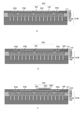
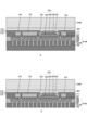
- FIG. 13 illustrates an example of a configuration of a sensor package according to a second embodiment
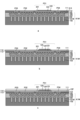
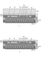
- FIG. 13 is a diagram illustrating a configuration example of a sensor package according to a third embodiment
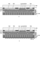
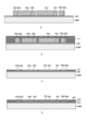
- FIG. 13 is a diagram illustrating a configuration example of a sensor package according to a fourth embodiment
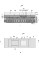
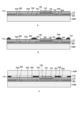
- FIG. 13 is a diagram illustrating a configuration example of a sensor package according to a fifth embodiment
- FIG. 23 is a diagram illustrating a configuration example of a sensor package according to a sixth embodiment.
- FIG. 13 illustrates an example of a configuration of a sensor package according to a second embodiment
- FIG. 13 is a diagram illustrating a configuration example of a sensor package according to a third embodiment
- FIG. 13 is a diagram illustrating a configuration example of a sensor package according to a fourth embodiment
- FIG. 13 is a diagram illustrating a configuration example of a sensor package according to a fifth embodiment
- FIG. 23 is a diagram illustrating a configuration example of a sensor package according to a sixth
- FIG. 23 is a diagram illustrating a configuration example of a sensor package according to a seventh embodiment.
- FIG. 23 is a diagram illustrating a configuration example of a sensor package according to an eighth embodiment.
- FIG. 23 is a diagram illustrating a configuration example of a sensor package according to a ninth embodiment.
- 13A to 13C are cross-sectional views showing an example of a manufacturing method for a sensor package according to a ninth embodiment.
- 13A to 13C are cross-sectional views showing an example of a manufacturing method for a sensor package according to a ninth embodiment.
- 13A to 13C are cross-sectional views showing an example of a manufacturing method for a sensor package according to a ninth embodiment.
- FIG. 23 is a diagram illustrating a configuration example of a sensor package according to a tenth embodiment.
- FIG. 23 is a diagram illustrating a configuration example of a sensor package according to an eleventh embodiment.
- FIG. 23 is a diagram illustrating a configuration example of a sensor package according to a twelfth embodiment.
- FIG. 23 is a diagram illustrating a configuration example of a sensor package according to a thirteenth embodiment.
- FIG. 23 is a diagram illustrating a configuration example of a sensor package according to a fourteenth embodiment.
- FIG. 23 is a diagram illustrating a configuration example of a sensor package according to a fifteenth embodiment.
- FIG. 23 is a diagram illustrating a configuration example of a sensor package according to a sixteenth embodiment.
- FIG. 23 is a diagram illustrating a configuration example of a sensor package according to a seventeenth embodiment.
- FIG. 23 is a diagram illustrating a configuration example of a sensor package according to an eighteenth embodiment.
- FIG. 23 is a diagram illustrating a configuration example of a sensor package according to a nineteenth embodiment.
- FIG. 23 is a diagram illustrating an example of the configuration of a sensor package according to a twentieth embodiment.
- FIG. 23 is a diagram illustrating an example of the configuration of a sensor package according to a twenty-first embodiment.
- FIG. 22 is a diagram illustrating an example of the configuration of a sensor package according to a twenty-second embodiment.
- FIG. 23 is a diagram illustrating an example of the configuration of a sensor package according to a twenty-third embodiment.
- FIG. 23 is a diagram illustrating an example of the configuration of a sensor package according to a twenty-fourth embodiment.
- FIG. 25 is a diagram illustrating an example of the configuration of a sensor package according to a twenty-fifth embodiment.
- FIG. 26 is a diagram illustrating an example of the configuration of a sensor package according to a twenty-sixth embodiment.
- 1 is a block diagram showing a schematic configuration example of a vehicle control system;
- FIG. 4 is an explanatory diagram showing an example of an installation position of an imaging unit.
- First embodiment an example in which a sensor chip having a sensor surface formed at the bottom of a recess on the back surface side and a semiconductor chip are flip-chip mounted on an interposer substrate, and a transparent substrate is disposed via a cavity on the sensor chip and the semiconductor chip
- Second embodiment an example in which a sensor chip having a sensor surface formed at the bottom of a recess on the back surface side and a semiconductor chip are flip-chip mounted on an interposer substrate, and a transparent substrate is disposed via a cavity on the sensor chip
- Third embodiment an example in which a sensor chip having a sensor surface formed at the bottom of a recess on the back surface side and a semiconductor chip are flip-chip mounted on an interposer substrate, and the sensor chip and the semiconductor chip are bonded to a transparent substrate via a transparent resin to make the structure cavityless
- Fourth embodiment an example in which a sensor chip having a sensor surface formed at the bottom of a recess on the back surface side and a semiconductor chip are flip-chip mounted on an interposer substrate, and a transparent substrate is disposed on the sensor chip and the semiconductor chip via a spacer
- Seventh embodiment (Example in which a plurality of different types of sensor chips and a semiconductor chip, each having a sensor surface formed at the bottom of a recess on the back surface side, are flip-chip mounted on an interposer substrate, and the sensor chips and the semiconductor chips are bonded to a transparent substrate via a transparent resin to make the structure cavityless) 8.
- Eighth embodiment (Example in which a plurality of different types of sensor chips and a semiconductor chip, each having a sensor surface formed at the bottom of a recess on the back surface side, are flip-chip mounted on an interposer substrate, and a transparent substrate is disposed on the sensor chips and the semiconductor chips via spacers) 9.
- Ninth embodiment an example in which a sensor chip having a sensor surface formed at the bottom of a recess on the back surface side and a semiconductor chip are flip-chip mounted on an interposer substrate, the semiconductor chip is covered with a sealing material, and a transparent substrate is disposed via a cavity on the sensor chip and the semiconductor chip.
- Tenth embodiment an example in which a sensor chip having a sensor surface formed at the bottom of a recess on the back surface side and a semiconductor chip are flip-chip mounted on an interposer substrate, the semiconductor chip is covered with a sealing material, and a transparent substrate is disposed via a cavity on the sensor chip) 11.
- Eleventh embodiment an example in which a sensor chip having a sensor surface formed at the bottom of a recess on the back surface side and a semiconductor chip are flip-chip mounted on an interposer substrate, the semiconductor chip is covered with a sealing material, and the sensor chip and the sealing material are bonded to a transparent substrate via a transparent resin to make the structure cavityless.
- Twelfth embodiment an example in which a sensor chip having a sensor surface formed at the bottom of a recess on the back surface side and a semiconductor chip are flip-chip mounted on an interposer substrate, the semiconductor chip is covered with a sealing material, and a transparent substrate is disposed on the sensor chip and the semiconductor chip via a spacer
- Twentieth embodiment an example in which a sensor chip and a semiconductor chip, which have been thinned together with a sealing material, are flip-chip mounted on an interposer substrate, and the sensor chip and the semiconductor chip are bonded to a transparent substrate via a transparent resin to make the structure cavityless
- 21st embodiment an example in which a sensor chip and a semiconductor chip, which have been thinned together with a sealing material, are flip-chip mounted on an interposer substrate, and a transparent substrate is disposed on the sensor chip and the semiconductor chip via a spacer 22.
- 26th embodiment an example in which a sensor chip thinned together with a sealing material and a semiconductor chip are mounted face-down on a rewiring layer, and a transparent substrate is disposed on the sensor chip and the semiconductor chip via a spacer.
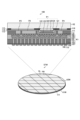
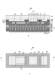
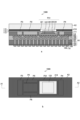
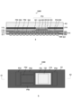
- the sensor package 100 is, for example, a SiP to which a chiplet is applied.
- the sensor package 100 includes a sensor chip P1 and semiconductor chips P2 to P6.
- the sensor element is formed on the sensor chip P1.
- the sensor element may be an image sensor such as a CCD (Charged Coupled Device) sensor, a CMOS (Complementary Metal-Oxide Semiconductor) sensor, or a SPAD (Single Photon Avalanche Diode) sensor.
- the light received by the image sensor may be visible light, near infrared light (NIR: Near InfraRed), short wave infrared light (SWIR: Short Wavelength InfraRed), ultraviolet light, or X-rays.
- the material used for the sensor element may be, for example, Si, InGaAs, InP, InSb, or HgCdTe.
- the sensor chip P1 includes a semiconductor substrate 121.
- a recess 122 is formed on the back side of the semiconductor substrate 121. In this case, taking into consideration misalignment of the recess 122 and variations in the opening width, the opening width of the recess 122 can be made smaller than the width of the semiconductor substrate 121.
- a sensor surface 123 is formed on the bottom of the recess 122. The sensor surface 123 can be sensitive to incident light.
- a back-illuminated image sensor may be formed on the sensor chip P1.
- pixels can be arranged in a matrix shape along the row direction and the column direction on the sensor surface 123.
- a photodiode and a pixel transistor can be formed in each pixel.
- a wiring layer is formed on the semiconductor substrate 121. The wiring layer can be bonded to the protruding electrode 112.
- a semiconductor element is formed in each of the semiconductor chips P2 to P6.
- the semiconductor element may include a transistor, a resistor, a capacitor, etc.
- a memory, a processor, a signal processing circuit, a data processing circuit, or an interface circuit may be formed.
- the processor may be single-core or multi-core.
- a hardware circuit such as an FPGA (Field-Programmable Gate Array) or an ASIC (Application Specific Integrated Circuit) may be formed.
- Each of the semiconductor chips P2 to P6 may be of different types or may include chips of the same type.
- the semiconductor chip P2 may be a core chip
- the semiconductor chips P3 and P4 may be memory chips
- the semiconductor chips P5 and P6 may be IO chips.
- the material used for the semiconductor element may be, for example, Si, GaAs, SiC, GaN, or InGaAsP.
- the sensor chip P1 and each of the semiconductor chips P2 to P6 are flip-chip mounted on the mounting surface of the interposer substrate K1 via the protruding electrodes 112.
- the sensor chip P1 and each of the semiconductor chips P2 to P6 are arranged at different positions on the interposer substrate K1. At this time, the distance between the sensor surface 123 of the sensor chip P1 and the mounting surface of the interposer substrate K1 can be shorter than the distance between the back surface of each of the semiconductor chips P2 to P6 and the mounting surface of the interposer substrate K1.
- the protruding electrodes 112 may be pillar electrodes or solder balls.
- the sensor chip P1 and each of the semiconductor chips P2 to P6 are collectively sealed with a sealing material 111.
- the sealing material 111 may be, for example, a mold resin or a potting material.
- the heights of the sensor chip P1, each of the semiconductor chips P2 to P6, and the sealing material 111 when the interposer substrate K1 is used as a reference can be made equal to one another. At this time, the back surfaces of the sensor chip P1 and each of the semiconductor chips P2 to P6 are exposed from the sealing material 111.
- the interposer substrate K1 includes a base substrate 101.
- the base substrate 101 may be, for example, a resin substrate, a Si substrate, a glass substrate, or a glass epoxy substrate.
- a wiring layer 103 is formed on the base substrate 101.
- a through electrode 102 is embedded in the base substrate 101 and is connected to the wiring layer 103.
- wiring 104 embedded in an insulating layer and a land electrode 105 are formed in the wiring layer 103.
- the land electrode 105 is exposed on the surface of the wiring layer 103.
- a via 106 used for interlayer connection is formed in the wiring layer 103.
- a protruding electrode 112 is bonded onto the land electrode 105.
- a through electrode 102 is connected to the wiring 104.
- An insulating layer 107 is formed on the rear surface of the base substrate 101.
- a land electrode 109 is formed on the insulating layer 107.
- a via 108 is embedded in the insulating layer 107. At this time, the land electrode 109 is connected to the through electrode 102 through the via 108.
- a protruding electrode 110 is formed on the land electrode 109.
- the protruding electrode 110 may be a pillar electrode or a solder ball.
- the material of the insulating layer 107 may be, for example, an inorganic material such as SiO 2 , SiN, or SiCN, or an organic material such as a solder resist.
- the wiring 104, the land electrodes 105, 109, and the vias 106, 108 may be made of a metal such as Al, Cu, AlCu, AlSiCu, or Co.
- the through electrode 102 may be made of a metal such as Cu, Ti, Ta, Al, W, Ni, Ru, or Co, or may have a layered structure of multiple materials.
- An underlayer 113 is formed on the sealing material 111 so as to cover the back surfaces of the sensor chip P1 and the semiconductor chips P2 to P6.
- the inner surface of the recess 122 of the semiconductor substrate 121 is covered with the underlayer 113.
- the underlayer 113 is formed on the sensor surface 123.
- the material of the underlayer 113 may be, for example, SiO2 or TEOS (Tetraethyl Orthosilicate).
- a light-shielding layer 124 is formed on the underlayer 113 on the sensor surface 123.
- the light-shielding layer 124 can be used for OPB (Opitical Black) pixels.
- the material of the light-shielding layer 124 may be a metal such as Al, Cu, Ag, Ti, or W, or a black resin.
- a protective film 114 is formed on the base layer 113 so as to cover the light-shielding layer 124.
- the material of the protective film 114 may be, for example, TEOS.
- a color filter 125 is formed for each pixel on the protective film 114 on the sensor surface 123.
- An on-chip lens 126 is formed for each pixel on the color filter 125.
- the material of the color filter 125 and the on-chip lens 126 can be, for example, an insulator such as SiO 2 , SiN, or SiCN, or a transparent resin such as acrylic or polycarbonate.
- the color filter 125 may contain a pigment.
- the color filter 125 may form, for example, a Bayer array or a quad Bayer array.
- the color filter 125 may include an RGB filter, a complementary color filter, or a white filter.
- a metasurface may be formed on the sensor surface 123.
- the metasurface may include a color splitter or a deflector.
- a protective film 115 is formed on the protective film 114 so as to cover the on-chip lens 126.
- the material of the protective film 115 may be, for example, LTO (Low Temperature Oxide) or polyimide.
- the transparent substrate K2 is bonded to the protective film 115 via the adhesive layer 116. At this time, a cavity is formed between the transparent substrate K2 and the protective film 115 on the rear surface side of each of the sensor chip P1 and the semiconductor chips P2 to P6. The height of the cavity may be longer on the sensor surface 123 than in the other areas.
- the transparent substrate K2 may be a glass substrate, a quartz substrate, or a transparent resin substrate such as acrylic or polycarbonate.
- the transparent substrate K2 may be made of Al 2 O 3 , CaF 2 , MgF 2 , or LiF depending on the wavelength detected by the sensor chip P1.
- the adhesive layer 116 may be a thermosetting resin such as epoxy, or may be an ultraviolet curing resin.
- the adhesive layer 116 may be blackened or composed of an opaque layer in order to reduce flare on the sensor surface 123.
- adhesive layer 116 may include a black pigment, such as carbon black, and may include a filler, such as carbon fiber.
- the transparent substrate K2 is chipped to have the same size as the interposer substrate K1.
- the position of the horizontal end of the transparent substrate K2 can be made to coincide with the position of the horizontal end of the interposer substrate K1.
- the position of the horizontal end of the interposer substrate K1 can be made to coincide with the position of the horizontal end of the sealing material 111.
- WLCSP Wafer Level Chip Size Package
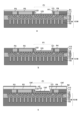
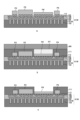
- FIGS. 2 to 8 are cross-sectional views showing an example of a method for manufacturing a sensor package according to the first embodiment.
- the interposer wafer K1W is laminated on the transparent substrate wafer K2W via the sealing material 111 that encapsulates the sensor chip P1 and the semiconductor chips P2 to P6.
- Partition regions PR are provided in the laminated wafer STW.
- Sensor packages 100 are cut out from each partition region PR.
- Each partition region PR is partitioned along a scribe line SL.
- the sensor packages 100 can be formed by dividing the laminated wafer STW along the scribe line SL.
- the interposer substrate K1 is cut out from the interposer wafer K1W.
- the transparent substrate K2 is cut out from the transparent substrate wafer K2W.
- the sensor chip P1' and each of the semiconductor chips P2 to P6 before the recess 122 is formed are flip-chip mounted on the interposer wafer K1W for each partition region PR.
- a resist pattern R1 having an opening H1 is formed on the sealing material 111 using lithography technology.
- the opening H1 can be positioned at the position where the sensor surface 123 is to be formed.
- the periphery of the back surface of the sensor chip P1' and the back surfaces of each of the semiconductor chips P2 to P6 can be covered with the resist pattern R1.
- the resist pattern R1 is removed by ashing or other methods.
- a base layer 113 is formed on the sealing material 111 by sputtering, CVD (Chemical Vapor Deposition) or other methods so as to cover the sensor surface 123.
- CVD Chemical Vapor Deposition
- a film of light-shielding material 124' is formed on the sensor surface 123 by a method such as sputtering. At this time, the light-shielding material 124' is also formed on the resist pattern R2.
- the light-shielding material 124' is caused to fly vertically toward the sensor surface 123, preventing the light-shielding material from wrapping around. This makes it possible to prevent the light-shielding material 124' from adhering to a position that is recessed from the reverse taper of the opening H2. This makes it possible to prevent the light-shielding material 124' from being formed on the side surface of the base layer 113 in the recess 122, thereby preventing the occurrence of flares and the like.
- a resist pattern R3 having an opening H3 is formed on the light-shielding material 124' based on lithography technology.
- the opening H3 can be located at a separation position of the light-shielding material 124'.
- the area on the base layer 113 where the light-shielding material 124' is not formed can be covered with the resist pattern R3.
- the light-shielding material 124' is etched using the resist pattern R3 as an etching mask, thereby forming the light-shielding layer 124 on the underlayer 113 on the sensor surface 123.
- anisotropic etching such as RIE can be used, for example.
- the resist pattern R3 is removed by ashing or other methods.
- a protective film 114 is formed on the underlayer 113 by sputtering, CVD or other methods so as to cover the light-shielding layer 124.
- a color filter 125 is formed for each pixel on the protective film 114 on the sensor surface 123.
- a lens material 126' is formed on the protective film 114 so as to cover the color filter 125.
- the lens material 126' can be planarized so that the surface of the protective film 114 is exposed.
- a resist pattern R4 having an opening H4 is formed on the protective film 114 using lithography technology.
- the opening H4 can be disposed on the sensor surface 123.
- the area on the protective film 114 where the lens material 126' is not yet formed can be covered with the resist pattern R4.
- the lens material 126' on the sensor surface 123 is thinned by etching the lens material 126' using the resist pattern R4 as an etching mask.
- anisotropic etching such as RIE can be used.
- the resist pattern R4 is removed by ashing or other methods.
- a resist pattern R5 having an opening H5 is formed on the lens material 126' based on lithography technology.
- the opening H5 can be located at the separation position of the on-chip lens 126.
- the unformed area of the lens material 126' on the protective film 114 can be covered with the resist pattern R5.
- the lens material 126' is etched using the resist pattern R5 as an etching mask to form the on-chip lens 126 on the sensor surface 123.
- anisotropic etching such as RIE can be used.
- a lens surface can be formed on the on-chip lens 126 based on the heat treatment and surface tension during etching of the lens material 126'.
- the resist pattern R5 is removed by ashing or other methods.
- a protective film 115 is formed on the protective film 114 by sputtering, CVD or other methods so as to cover the on-chip lens 126.
- an adhesive layer 116 is formed on the protective film 115.
- the adhesive layer 116 can be disposed on the periphery of the sensor chip P1 and on the periphery of the sensor package 100.
- the adhesive layer 116 may also be disposed on the scribe line SL.
- the adhesive layer 116 may be formed by potting, printing, or inkjet.
- the transparent substrate wafer K2W is bonded to the protective film 115 via the adhesive layer 116. Then, the adhesive layer 116 is hardened to fix the transparent substrate wafer K2W to the protective film 115.
- the back side of the interposer wafer K1W is thinned to expose the through electrodes 102.
- This thinning may be performed using CMP, back grinding, or etch-back.
- a protective film may be attached to the transparent substrate wafer K2W to prevent scratches from being formed on the transparent substrate wafer K2W.
- an insulating layer 107 is formed on the interposer wafer K1W. Then, after vias 108 are embedded in the insulating layer 107, land electrodes 109 connected to the vias 108 are formed on the insulating layer 107. Furthermore, protruding electrodes 110 are formed on the land electrodes 109. At this time, a stacked wafer STW is formed before being diced into sensor packages 100.
- the laminated wafer STW is cut along the scribe lines SL to separate the sensor packages 100.
- the laminated wafer STW may be cut by dicing or by using a laser cutter.
- the through electrodes 102 are formed in the interposer wafer K1W before the sensor chip P1' and each of the semiconductor chips P2 to P6 are collectively sealed with the sealing material 111.
- the through electrodes 102 may be formed in the interposer wafer K1W after the sensor chip P1' and each of the semiconductor chips P2 to P6 are collectively sealed with the sealing material 111.
- the sensor chip P1 with the sensor surface 123 formed at the bottom of the recess 122 and the semiconductor chips P2 to P6 are flip-chip mounted on the interposer substrate K1, and the transparent substrate K2 is arranged through the cavities on the sensor chip P1 and the semiconductor chips P2 to P6.
- the sensor chip P1 and the semiconductor chips P2 to P6 are flip-chip mounted on the interposer substrate K1, and the transparent substrate K2 is disposed via the cavities on the sensor chip P1 and the semiconductor chips P2 to P6.
- the sensor chip P1 and the semiconductor chips P2 to P6 are flip-chip mounted on the interposer substrate K1, and the transparent substrate K2 is disposed via the cavity on the sensor chip P1.
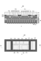
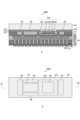
- FIG. 9 is a diagram showing an example of the configuration of a sensor package according to the second embodiment.
- a is a cross-sectional view showing the example of the configuration of a sensor package according to the second embodiment
- b in the figure is a plan view showing the example of the configuration of a sensor package according to the second embodiment.
- the sensor package 200 has an adhesive layer 216 instead of the adhesive layer 116 of the first embodiment described above.
- the rest of the configuration of the sensor package 200 of the second embodiment is the same as the configuration of the sensor package 100 of the first embodiment described above.
- the transparent substrate K2 is supported on the sensor chip P1 and the semiconductor chips P2 to P6 via the adhesive layer 216, and a cavity is provided on the sensor chip P1.
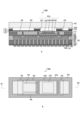
- the sensor package 300 has a transparent resin 316 instead of the adhesive layer 116 of the first embodiment described above.
- the rest of the configuration of the sensor package 300 of the third embodiment is the same as the configuration of the sensor package 100 of the first embodiment described above.
- the transparent substrate K2 is bonded to the protective film 115 via the transparent resin 316.
- the transparent resin 316 is formed on the entire surface of the protective film 115. At this time, the transparent resin 316 is also filled into the recess 122.
- the space between the transparent substrate K2 and the protective film 115 is made cavity-less.
- the transparent resin 316 may be a thermosetting resin or an ultraviolet curing resin.
- the material of the transparent resin 316 may be, for example, a siloxane-based resin, an acrylic-based resin, or an epoxy-based resin. In this case, the material of the transparent resin 316 may be selected so as to ensure a refractive index difference between the on-chip lens 126.
- the transparent resin 316 may contain a filler made of an inorganic or organic substance to improve reliability. A material with adjusted optical properties (refractive index, extinction coefficient, etc.) may be selected for the transparent resin 316 so that light can be received well in the effective pixel area.
- the sensor chip P1 and the semiconductor chips P2 to P6 are bonded to the transparent substrate K2 via the transparent resin 316, making the sensor surface 123 cavity-less.
- the transparent substrate K2 is supported on the sensor chip P1 and the semiconductor chips P2 to P6 via the adhesive layer 116.
- a spacer is provided between the adhesive layer 116 and the transparent substrate K2.
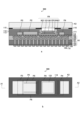
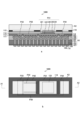
- FIG. 11 is a diagram showing an example of the configuration of a sensor package according to the fourth embodiment.
- a is a cross-sectional view showing the example of the configuration of a sensor package according to the fourth embodiment
- b in the figure is a plan view showing the example of the configuration of a sensor package according to the fourth embodiment.
- the sensor package 400 is the sensor package 100 of the first embodiment described above, to which a spacer 416 has been added.
- the rest of the configuration of the sensor package 400 of the fourth embodiment is similar to the configuration of the sensor package 100 of the first embodiment described above.
- the spacer 416 is provided between the adhesive layer 116 and the transparent substrate K2.
- the planar shape of the spacer 416 may be the same as the planar shape of the adhesive layer 116.
- the spacer 416 can be bonded to the transparent substrate K2.
- the adhesive layer 116 and the spacer 416 can secure cavities on the sensor chip P1 and on the semiconductor chips P2 to P6.
- the material of the spacer 416 may be a resin such as epoxy, or a metal such as stainless steel.
- the spacer 416 may be blackened to reduce flare on the sensor surface 123.
- a spacer 416 is provided between the adhesive layer 116 and the transparent substrate K2. This makes it possible to adjust the height of the cavities on the sensor chip P1 and on the semiconductor chips P2 to P6, and thus to adjust the optical characteristics on the sensor surface 123.
- a spacer 416 was provided between the adhesive layer 116 and the transparent substrate K2 in the first embodiment described above, but a spacer may also be provided between the adhesive layer 216 and the transparent substrate K2 in the second embodiment described above.
- a single sensor chip P1 and semiconductor chips P2 to P6 are flip-chip mounted on the interposer substrate K1.
- a plurality of sensor chips and semiconductor chips are flip-chip mounted on the interposer substrate K1, and a transparent substrate is disposed via cavities on the plurality of sensor chips and the semiconductor chip.
- FIG. 12 is a diagram showing an example of the configuration of a sensor package according to the fifth embodiment.
- a in the figure is a cross-sectional view showing the example of the configuration of a sensor package according to the fifth embodiment
- b in the figure is a plan view showing the example of the configuration of a sensor package according to the fifth embodiment.
- the cross-sectional view in a in the figure is taken at the position of line B1-B2 in b in the figure.
- the sensor package 500 includes sensor chips P11, P12, semiconductor chips P13 to P18, interposer substrate K5, and transparent substrate K6 instead of the sensor chip P1, semiconductor chips P2 to P6, interposer substrate K1, and transparent substrate K2 of the first embodiment described above.
- the rest of the configuration of the sensor package 500 of the fifth embodiment is the same as the configuration of the sensor package 100 of the first embodiment described above.
- the sensor chip P11 can be configured in the same manner as the sensor chip P1.
- a light-shielding layer 124, a color filter 125, and an on-chip lens 126 can be formed on the sensor surface 123 of the sensor chip P11.
- a sensor element is formed on the sensor chip P12.
- the sensor chip P12 is of a different type from the sensor chip P11.
- the sensitivity band of the sensor chip P12 may be different from the sensitivity band of the sensor chip P11
- the sensor chip P12 may be an infrared sensor and the sensor chip P11 may be a visible light sensor.
- the sensor chip P11 may be a CMOS image sensor and the sensor chip P12 may be an EVS (Event-based Vision Sensor).
- the planar size of the sensor chip P12 may be different from the planar size of the sensor chip P11.
- the sensor chip P12 includes a semiconductor substrate 521.
- a recess 522 is formed on the rear side of the semiconductor substrate 521.
- a sensor surface 523 is formed at the bottom of the recess 522. The sensor surface 523 can be sensitive to incident light.
- a wiring layer that is bonded to the protruding electrode 112 is formed on the semiconductor substrate 521.
- a semiconductor element is formed in each of the semiconductor chips P13 to P18.
- the types of the semiconductor chips P13 to P18 may be different from each other, or may include the same type of chips.
- the semiconductor chips P15 and P18 may be core chips
- the semiconductor chips P16 and P17 may be memory chips
- the semiconductor chips P13 and P14 may be IO chips.
- the sensor chips P11, P12 and the semiconductor chips P13 to P18 are flip-chip mounted on the mounting surface of the interposer substrate K5 via the protruding electrodes 112.
- the sensor chips P11, P12 and the semiconductor chips P13 to P18 are arranged at different positions on the interposer substrate K5.
- the sensor chips P11, P12 and the semiconductor chips P13 to P18 are collectively sealed with the sealing material 111.
- the interposer substrate K5 includes a base substrate 501.
- a wiring layer 503 is formed on the base substrate 501.
- a through electrode 102 is embedded in the base substrate 501 and connected to the wiring layer 503.
- Wiring 104 and land electrodes 105 are formed in the wiring layer 503.
- a via 106 used for interlayer connection is formed in the wiring layer 503.
- An insulating layer 107 is formed on the rear surface of the base substrate 501.
- a base layer 113 is formed on the sealing material 111 so as to cover the back surfaces of the sensor chips P11, P12 and the semiconductor chips P13 to P18.
- the inner surfaces of the recesses 122, 522 of each semiconductor substrate 121, 521 are covered with the base layer 113.
- the base layer 113 is formed on each sensor surface 123, 523.
- a light-shielding layer 524 is formed on the base layer 113.
- a protective film 114 is formed on the base layer 113 so as to cover the light-shielding layers 124, 524.
- An on-chip lens 526 is formed for each pixel on the protective film 114 on the sensor surface 523.
- a protective film 115 is formed on the protective film 114 so as to cover the on-chip lenses 126, 526.
- the transparent substrate K6 is bonded to the protective film 115 via the adhesive layer 116. At this time, cavities are formed between the transparent substrate K6 and the protective film 115 on the back surface side of each of the sensor chips P11, P12 and the semiconductor chips P13 to P18.
- the transparent substrate K6 is chipped to have the same size as the interposer substrate K5. At this time, the position of the horizontal end of the transparent substrate K6 can be made to coincide with the position of the horizontal end of the interposer substrate K5. In addition, the position of the horizontal end of the interposer substrate K5 can be made to coincide with the position of the horizontal end of the sealing material 111. This allows the sensor package 500 to constitute a WLCSP packaged at the wafer level.
- the sensor chips P11, P12 and the semiconductor chips P13 to P18 are flip-chip mounted on the interposer substrate K5, and the transparent substrate K6 is disposed via the cavities above the sensor chips P11, P12 and the semiconductor chips P13 to P18.
- the sensor chips P11, P12 and the semiconductor chips P13 to P18 are flip-chip mounted on the interposer substrate K5, and the transparent substrate K6 is disposed via the cavities above the sensor chips P11, P12.
- FIG. 13 is a diagram showing an example of the configuration of a sensor package according to the sixth embodiment.
- a is a cross-sectional view showing the example of the configuration of a sensor package according to the sixth embodiment
- b in the figure is a plan view showing the example of the configuration of a sensor package according to the sixth embodiment.
- the sensor package 600 has an adhesive layer 216 instead of the adhesive layer 116 of the fifth embodiment described above.
- the rest of the configuration of the sensor package 600 of the sixth embodiment is the same as the configuration of the sensor package 500 of the fifth embodiment described above.
- the transparent substrate K6 is bonded to the protective film 115 via an adhesive layer 216. At this time, a cavity is formed between the transparent substrate K6 and the protective film 115 on the back surface side of each of the sensor chips P11 and P12.
- the rest of the configuration of the adhesive layer 216 in the sixth embodiment is the same as the configuration of the adhesive layer 116 in the fifth embodiment described above.
- the transparent substrate K6 is supported on the sensor chips P11, P12 and the semiconductor chips P13 to P18 via the adhesive layer 216, and a cavity is provided on each of the sensor chips P11, P12.
- the transparent substrate K6 is supported on the sensor chips P11, P12 and the semiconductor chips P13 to P18 via the adhesive layer 116, and cavities are provided on the sensor chips P11, P12 and the semiconductor chips P13 to P18.
- the sensor chips P11, P12 and the semiconductor chips P13 to P18 are flip-chip mounted on the interposer substrate K5, and the sensor chips P11, P12 and the semiconductor chips P13 to P18 are bonded to the transparent substrate K6 via the transparent resin 316 to make the cavity-less.
- FIG. 14 is a diagram showing an example of the configuration of a sensor package according to the seventh embodiment.
- a is a cross-sectional view showing the example of the configuration of a sensor package according to the seventh embodiment
- b in the figure is a plan view showing the example of the configuration of a sensor package according to the seventh embodiment.
- the sensor package 700 has a transparent resin 316 instead of the adhesive layer 116 of the fifth embodiment described above.
- the rest of the configuration of the sensor package 700 of the seventh embodiment is the same as the configuration of the sensor package 500 of the fifth embodiment described above.
- the transparent substrate K6 is bonded to the protective film 115 via the transparent resin 316.
- the transparent resin 316 is formed on the entire surface of the protective film 115. At this time, the transparent resin 316 also fills the recesses 122 and 521.
- the space between the transparent substrate K6 and the protective film 115 is made cavity-less.
- the sensor chips P11, P12 and the semiconductor chips P13 to P18 are bonded to the transparent substrate K6 via the transparent resin 316, making the sensor surfaces 123, 523 cavity-less.
- This makes it possible to receive light on the sensor surfaces 123, 523 while eliminating the need for a cavity in the sensor package 700, improving the strength of the sensor package 700, and eliminating the need to form the transparent resin 316 so as to avoid the sensor surfaces 123, 523, simplifying the manufacturing process.
- the transparent substrate K2 is supported on the sensor chips P11, P12 and the semiconductor chips P13 to P18 via the adhesive layer 116.
- a spacer 416 is provided between the adhesive layer 116 and the transparent substrate K2.
- FIG. 15 is a diagram showing an example of the configuration of a sensor package according to the eighth embodiment.
- a is a cross-sectional view showing the example of the configuration of a sensor package according to the eighth embodiment
- b in the figure is a plan view showing the example of the configuration of a sensor package according to the second embodiment.
- the sensor package 800 is the sensor package 500 of the fifth embodiment described above, to which a spacer 416 has been added.
- the rest of the configuration of the sensor package 800 of the eighth embodiment is the same as the configuration of the sensor package 500 of the fifth embodiment described above.
- the spacer 416 is provided between the adhesive layer 116 and the transparent substrate K6.
- the spacer 416 can be bonded to the transparent substrate K6.
- the adhesive layer 116 and the spacer 416 can secure cavities above the sensor chips P11, P12 and the semiconductor chips P13 to P18.
- a spacer 416 is provided between the adhesive layer 116 and the transparent substrate K6. This allows the height of the cavities on the sensor chips P11, P12 and the semiconductor chips P13 to P18 to be adjusted, and the optical characteristics on each sensor surface 123, 523 to be adjusted.
- a spacer 416 was provided between the adhesive layer 116 and the transparent substrate K6 in the fifth embodiment described above, but a spacer may also be provided between the adhesive layer 216 and the transparent substrate K6 in the sixth embodiment described above.
- the sensor chip P1 having the sensor surface 123 formed on the bottom of the recess 122 and the semiconductor chips P2 to P6 are flip-chip mounted on the interposer substrate K1, and the back sides of the sensor chip P1 and the semiconductor chips P2 to P6 are exposed from the sealing material 111.
- the sensor chip having the sensor surface 123 formed on the bottom of the recess and the semiconductor chips P2 to P6 are flip-chip mounted on the interposer substrate K1, and the back sides of the semiconductor chips P2 to P6 are covered with the sealing material 111 and the back sides of the sensor chips are exposed from the sealing material 111.
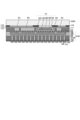
- FIG. 16 is a diagram showing an example of the configuration of a sensor package according to the ninth embodiment.
- a is a cross-sectional view showing the example of the configuration of a sensor package according to the ninth embodiment
- b in the figure is a plan view showing the example of the configuration of a sensor package according to the ninth embodiment.
- the sensor package 900 includes a sensor chip P9 instead of the sensor chip P1 of the first embodiment described above.
- the rest of the configuration of the sensor package 900 of the ninth embodiment is the same as the configuration of the sensor package 100 of the first embodiment described above.
- the sensor chip P9 includes a semiconductor substrate 921 instead of the semiconductor substrate 121 of the first embodiment described above.
- the thickness of the semiconductor substrate 921 can be thinner than the thickness of the semiconductor substrate 121.
- the semiconductor substrate 921 includes a recess 922 instead of the recess 122 of the first embodiment described above.
- a sensor surface 123 is formed at the bottom of the recess 922.
- the depth of the recess 922 can be shallower than the depth of the recess 122.
- the rest of the configuration of the sensor chip P9 of the ninth embodiment is the same as the configuration of the sensor chip P1 of the first embodiment described above.
- the sensor chip P9 and each of the semiconductor chips P2 to P6 are flip-chip mounted on the mounting surface of the interposer substrate K1 via the protruding electrodes 112.
- the sensor chip P9 and each of the semiconductor chips P2 to P6 are collectively sealed with a sealing material 111.
- the back sides of the semiconductor chips P2 to P6 are covered with the sealing material 111, and the back side of the sensor chip P9 is exposed from the sealing material 111.
- at least one of the semiconductor chips P2 to P6 may have a different height when the mounting surface of the interposer substrate K1 is used as a reference.
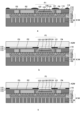
- FIGS. 17 to 21 are cross-sectional views showing an example of a method for manufacturing a sensor package according to the ninth embodiment.
- the sensor chip P9' and each of the semiconductor chips P2 to P6 are flip-chip mounted on the interposer wafer K1W for each partition region PR. Note that this figure shows an example in which the heights of the sensor chip P9' and each of the semiconductor chips P2 to P4 are different from each other.
- protective tape PT is placed on the sensor chip P9'.
- the protective tape PT may be attached to the sensor chip P9' to prevent misalignment.
- the shape of the protective tape PT may be a rectangular parallelepiped.
- the planar size of the protective tape PT may be equal to the planar size of the sensor chip P9'.
- the material of the protective tape PT may be, for example, a heat-resistant resin.
- the mold die MK is positioned so as to be in contact with the protective tape PT and face the interposer wafer K1W. Then, the sealing material 111 is injected between the interposer wafer K1W and the mold die MK and cured. At this time, the sensor chip P9' and each of the semiconductor chips P2 to P6 in each partitioned region PR are collectively sealed with the sealing material 111.
- the mold die MK is removed from the sealing material 111, and the protective tape PT is removed from the sensor chip P9'.
- a resist pattern R11 having an opening H11 is formed on the sealing material 111.
- the opening H11 can be positioned at the position where the sensor surface 123 is to be formed.
- the periphery of the back surface of the sensor chip P9' and the back surfaces of each of the semiconductor chips P2 to P6 can be covered with the resist pattern R11.
- the semiconductor substrate 921 of the sensor chip P9' is etched using the resist pattern R11 as an etching mask, thereby forming a recess 922 on the back side of the semiconductor substrate 921.
- the sensor surface 123 can be formed at the bottom of the recess 922.
- a base layer 113 is formed on the sealing material 111 so as to cover the sensor surface 123.
- the back surface of the sensor chip P9 and the back surfaces of each of the semiconductor chips P2 to P6 can be covered with the base layer 113.
- a resist pattern R12 having an opening H12 is formed on the base layer 113.
- the opening H12 can be disposed on the sensor surface 123.
- the end of the opening H12 can be formed in an inverse tapered shape.
- a light-shielding material 124' is deposited on the sensor surface 123.
- the light-shielding material 124' is also deposited on the resist pattern R12.
- the resist pattern R12 is removed using a stripping solution, and the light-shielding material 124' on the resist pattern R12 is lifted off.
- a resist pattern R13 having an opening H13 is formed on the light-shielding material 124'.
- the opening H13 can be arranged at a separation position of the light-shielding material 124'. At this time, the area on the base layer 113 where the light-shielding material 124' is not formed can be covered with the resist pattern R13.
- the light-shielding material 124' is etched using the resist pattern R13 as an etching mask to form a light-shielding layer 124 on the base layer 113 on the sensor surface 123.
- a protective film 114 is formed on the underlayer 113 so as to cover the light-shielding layer 124. Furthermore, a color filter 125 is formed for each pixel on the protective film 114 on the sensor surface 123.
- a lens material 126' is formed on the protective film 114 so as to cover the color filter 125.
- the lens material 126' can be planarized so that the surface of the protective film 114 is exposed.
- the lens material 126' on the sensor surface 123 is thinned, and then the lens material 126' is processed to form an on-chip lens 126 for each pixel on the sensor surface 123.
- a protective film 115 is formed on the protective film 114 so as to cover the on-chip lens 126.
- an adhesive layer 116 is formed on the protective film 115.
- the adhesive layer 116 can be disposed on the periphery of the sensor chip P9 and the periphery of the sensor package 900.
- the back side of the interposer wafer K1W is thinned to expose the through electrodes 102.
- an insulating layer 107 is formed on the interposer wafer K1W. Then, after vias 108 are embedded in the insulating layer 107, land electrodes 109 connected to the vias 108 are formed on the insulating layer 107. Furthermore, protruding electrodes 110 are formed on the land electrodes 109.
- the laminated wafer in which the sensor chip P9 and the semiconductor chips P2 to P6 are arranged between the interposer wafer K1W and the transparent substrate wafer K2W is cut along the scribe lines SL to separate the sensor packages 900.
- the sensor chip P9 having the sensor surface 123 formed on the bottom of the recess 922 and the semiconductor chips P2 to P6 are flip-chip mounted on the interposer substrate K1, the back sides of the semiconductor chips P2 to P6 are covered with the sealing material 111, and the back side of the sensor chip P9 is exposed from the sealing material 111.
- the transparent substrate K2 is disposed via the cavities on the sensor chip P9 and the semiconductor chips P2 to P6, the back sides of the semiconductor chips P2 to P6 are covered with the sealing material 111, and the back side of the sensor chip P9 is exposed from the sealing material 111.
- the transparent substrate K2 is disposed via the cavity on the sensor chip P9, the back sides of the semiconductor chips P2 to P6 are covered with the sealing material 111, and the back side of the sensor chip P9 is exposed from the sealing material 111.
- FIG. 22 is a diagram showing an example of the configuration of a sensor package according to the tenth embodiment.
- a is a cross-sectional view showing the example of the configuration of a sensor package according to the tenth embodiment
- b in the figure is a plan view showing the example of the configuration of a sensor package according to the tenth embodiment.
- the sensor package 1000 has an adhesive layer 216 instead of the adhesive layer 116 of the ninth embodiment described above.
- the rest of the configuration of the sensor package 1000 of the tenth embodiment is the same as the configuration of the sensor package 900 of the ninth embodiment described above.
- the transparent substrate K2 is bonded to the protective film 115 via the adhesive layer 216. At this time, a cavity is formed between the transparent substrate K2 and the protective film 115 on the back side of the sensor chip P9.
- the rest of the configuration of the adhesive layer 216 in the tenth embodiment is the same as the configuration of the adhesive layer 116 in the ninth embodiment described above.
- the transparent substrate K2 is supported on the sensor chip P9 and the semiconductor chips P2 to P6 via the adhesive layer 216, and a cavity is provided on the sensor chip P9.
- the transparent substrate K2 is supported on the sensor chip P9 and the semiconductor chips P2 to P6 via the adhesive layer 116, and cavities are provided on the sensor chip P9 and the semiconductor chips P2 to P6.
- the sensor chip P9 and the semiconductor chips P2 to P6 are flip-chip mounted on the interposer substrate K1, and the sensor chip P9 and the semiconductor chips P2 to P6 are bonded to the transparent substrate K2 via the transparent resin 316 to make the cavity-less.
- a is a cross-sectional view showing the example of the configuration of a sensor package according to the 11th embodiment
- b is a plan view showing the example of the configuration of a sensor package according to the 11th embodiment.
- the sensor package 1100 has a transparent resin 316 instead of the adhesive layer 116 of the ninth embodiment described above.
- the rest of the configuration of the sensor package 1100 of the eleventh embodiment is the same as the configuration of the sensor package 900 of the ninth embodiment described above.
- the transparent substrate K2 is bonded to the protective film 115 via the transparent resin 316.
- the transparent resin 316 is formed on the entire surface of the protective film 115. At this time, the transparent resin 316 also fills the recess 922.
- the space between the transparent substrate K2 and the protective film 115 is made cavity-less.
- the sensor chip P9 and the semiconductor chips P2 to P6 are bonded to the transparent substrate K2 via the transparent resin 316, making the sensor surface 123 cavity-less.
- This makes it possible to receive light on the sensor surface 123 while eliminating the need for a cavity in the sensor package 1100, which improves the strength of the sensor package 1100 and eliminates the need to form the transparent resin 316 so as to avoid the sensor surface 123, simplifying the manufacturing process.
- Twelfth embodiment In the above-mentioned ninth embodiment, in order to provide cavities on the sensor chip P9 and the semiconductor chips P2 to P6, the transparent substrate K2 is supported on the sensor chip P9 and the semiconductor chips P2 to P6 via the adhesive layer 116. In this twelfth embodiment, in order to adjust the height of the cavities on the sensor chip P9 and the semiconductor chips P2 to P6, a spacer 416 is provided between the adhesive layer 116 and the transparent substrate K2.
- FIG. 24 is a diagram showing an example of the configuration of a sensor package according to the 12th embodiment.
- a is a cross-sectional view showing the example of the configuration of a sensor package according to the 12th embodiment
- b in the figure is a plan view showing the example of the configuration of a sensor package according to the 12th embodiment.
- the sensor package 1200 is the sensor package 900 of the ninth embodiment described above, to which a spacer 416 has been added.
- the rest of the configuration of the sensor package 1200 of the twelfth embodiment is the same as the configuration of the sensor package 900 of the ninth embodiment described above.
- the spacer 416 is provided between the adhesive layer 116 and the transparent substrate K2. At this time, the adhesive layer 116 and the spacer 416 can secure cavities on the sensor chip P9 and on the semiconductor chips P2 to P6.
- a spacer 416 is provided between the adhesive layer 116 and the transparent substrate K2. This makes it possible to adjust the height of the cavities on the sensor chip P9 and on the semiconductor chips P2 to P6, and thus to adjust the optical characteristics on the sensor surface 123.
- the sensor chip P1 and the semiconductor chips P2 to P6 are flip-chip mounted on the interposer substrate K1 via the protruding electrodes 110.
- the sensor chip and the semiconductor chip are mounted face-down on the interposer substrate and directly bonded to each other.
- FIG. 25 is a diagram showing an example of the configuration of a sensor package according to the 13th embodiment.
- a is a cross-sectional view showing the example of the configuration of a sensor package according to the 13th embodiment
- b in the figure is a plan view showing the example of the configuration of a sensor package according to the 13th embodiment.
- the sensor package 1300 includes a sensor chip P21, semiconductor chips P22 to P26, and an interposer substrate K21, instead of the sensor chip P1, semiconductor chips P2 to P6, and interposer substrate K1 of the first embodiment described above.
- the rest of the configuration of the sensor package 1300 of the thirteenth embodiment is the same as the configuration of the sensor package 100 of the first embodiment described above.
- the sensor chip P21 includes a semiconductor substrate 121.
- a bonding electrode 131 is formed in a wiring layer on the semiconductor substrate 121. The surface of the bonding electrode 131 is exposed from the wiring layer on the semiconductor substrate 121.
- the rest of the configuration of the sensor chip P21 of the thirteenth embodiment is the same as the configuration of the sensor chip P1 of the first embodiment described above.
- a semiconductor element is formed in each of the semiconductor chips P22 to P26.
- a bonding electrode is formed in the wiring layer of each of the semiconductor chips P22 to P26. The surface of the bonding electrode of each of the semiconductor chips P22 to P26 is exposed from the wiring layer of each of the semiconductor chips P22 to P26.
- bonding electrodes 132 to 134 are formed in the wiring layer of each of the semiconductor chips P22 to P24.
- the other configurations of each of the semiconductor chips P22 to P26 in the thirteenth embodiment are similar to the configuration of each of the semiconductor chips P2 to P6 in the first embodiment described above.
- the interposer substrate K21 includes a base substrate 101.
- a wiring layer 203 is formed on the base substrate 101.
- a through electrode 102 is embedded in the base substrate 101 and connected to the wiring layer 203.
- a wiring 204 embedded in an insulating layer and a bonding electrode 205 are formed in the wiring layer 203.
- the surface of the bonding electrode 205 is exposed from the wiring layer 203.
- a via 206 used for interlayer connection is formed in the wiring layer 203.
- the rest of the configuration of the interposer substrate K21 of the thirteenth embodiment is the same as the configuration of the interposer substrate K1 of the first embodiment described above.
- the sensor chip P21 and the semiconductor chips P22 to P26 are mounted face-down on the interposer substrate K21 and directly bonded to each other. This makes it possible to increase the arrangement density of the connection terminals between the sensor chip P21 and each of the semiconductor chips P22 to P24 and the interposer substrate K21 while suppressing a decrease in bonding strength.
- the configuration in which the sensor chip P21 and the semiconductor chips P22 to P26 are directly bonded to the interposer substrate K21 is applied to the above-mentioned first embodiment.
- the configuration in which the sensor chip P21 and the semiconductor chips P22 to P26 are directly bonded to the interposer substrate K21 may be applied to any of the configurations of the above-mentioned second to twelfth embodiments.
- the recess 122 is formed on the back surface side of the sensor chip P1, and the sensor surface 123 is provided at the bottom of the recess 122.
- the sensor chip whose entire back surface on which the sensor surface 123 is formed is thinned and the semiconductor chips P2 to P6 are collectively sealed with the sealing material 111.
- FIG. 26 is a diagram showing an example of the configuration of a sensor package according to the 14th embodiment.
- a is a cross-sectional view showing the example of the configuration of a sensor package according to the 14th embodiment
- b in the figure is a plan view showing the example of the configuration of a sensor package according to the 14th embodiment.
- the sensor package 1400 includes a sensor chip P31 instead of the sensor chip P1 of the first embodiment described above.
- the rest of the configuration of the sensor package 1400 of the fourteenth embodiment is the same as the configuration of the sensor package 100 of the first embodiment described above.
- the sensor chip P31 includes a semiconductor substrate 321.
- the back surface of the semiconductor substrate 321 is planarized.
- a sensor surface 123 is formed on the back surface of the semiconductor substrate 321.
- the planar size of the sensor surface 123 can be smaller than the planar size of the semiconductor substrate 321.
- the rest of the configuration of the sensor chip P31 is the same as the configuration of the sensor chip P1 of the first embodiment described above.
- the sensor chip P31 and each of the semiconductor chips P2 to P6 are flip-chip mounted on the mounting surface of the interposer substrate K1 via the protruding electrodes 112. On the interposer substrate K1, the sensor chip P31 and each of the semiconductor chips P2 to P6 are collectively sealed with a sealing material 111. A cavity is formed between the transparent substrate K2 and the protective film 115 on the back surface side of each of the sensor chip P31 and the semiconductor chips P2 to P6.
- FIG. 27 is a cross-sectional view showing an example of a method for manufacturing a sensor package according to the fourteenth embodiment.
- step in FIG. 27 is provided instead of step a in FIG. 4 in the method for manufacturing a sensor package according to the first embodiment described above.
- the other steps in the method for manufacturing a sensor package according to the fourteenth embodiment are the same as the steps in the method for manufacturing a sensor package according to the first embodiment described above.
- a resist pattern R31 with an opening H31 is formed on the sealing material 111 using lithography technology.
- the opening H31 can be positioned at the position of the sensor chip P31.
- the back surface of each of the semiconductor chips P2 to P6 can be covered with the resist pattern R31.
- the semiconductor substrate 321 of the sensor chip P31 is etched using the resist pattern R31 as an etching mask, thereby thinning the entire back surface of the semiconductor substrate 321.
- the sensor surface 123 can be formed on the back surface of the semiconductor substrate 321.
- the sensor chip P31 whose entire back surface on which the sensor surface 123 is formed has been thinned, and the semiconductor chips P2 to P6 are collectively sealed with the sealing material 111. This makes it possible to eliminate the need for the recess 122 on the back surface side of the sensor chip P31, and reduces the stress concentration on the sensor chip P31.
- the sensor chip P31 whose entire back surface on which the sensor surface 123 is formed is thinned, and the semiconductor chips P2 to P6 are collectively sealed with the sealing material 111, and the transparent substrate K2 is arranged via the cavity on the sensor chip P31 and the semiconductor chips P2 to P6.
- the sensor chip P31 whose entire back surface on which the sensor surface 123 is formed is thinned, and the semiconductor chips P2 to P6 are collectively sealed with the sealing material 111, and the transparent substrate K2 is arranged via the cavity on the sensor chip P31.
- FIG. 28 is a diagram showing an example of the configuration of a sensor package according to the fifteenth embodiment.
- a is a cross-sectional view showing the example of the configuration of a sensor package according to the fifteenth embodiment
- b in the figure is a plan view showing the example of the configuration of a sensor package according to the fifteenth embodiment.
- the sensor package 1500 has an adhesive layer 216 instead of the adhesive layer 116 of the above-mentioned fourteenth embodiment.
- the rest of the configuration of the sensor package 1500 of the fifteenth embodiment is the same as the configuration of the sensor package 1400 of the above-mentioned fourteenth embodiment.
- the transparent substrate K2 is bonded to the protective film 115 via the adhesive layer 216. At this time, a cavity is formed between the transparent substrate K2 and the protective film 115 on the back surface side of the sensor chip P31.
- the rest of the configuration of the adhesive layer 216 in the fifteenth embodiment is the same as the configuration of the adhesive layer 116 in the fourteenth embodiment described above.
- the transparent substrate K2 is supported on the sensor chip P31 and the semiconductor chips P2 to P6 via the adhesive layer 216, and a cavity is provided on the sensor chip P31.
- the transparent substrate K2 is supported on the sensor chip P31 and the semiconductor chips P2 to P6 via the adhesive layer 116, and cavities are provided on the sensor chip P31 and the semiconductor chips P2 to P6.
- the sensor chip P31 and the semiconductor chips P2 to P6 are flip-chip mounted on the interposer substrate K1, and the sensor chip P31 and the semiconductor chips P2 to P6 are bonded to the transparent substrate K2 via the transparent resin 316 to make the cavity-less.
- FIG. 29 is a diagram showing an example of the configuration of a sensor package according to the 16th embodiment.
- a is a cross-sectional view showing the example of the configuration of a sensor package according to the 16th embodiment
- b in the figure is a plan view showing the example of the configuration of a sensor package according to the 16th embodiment.
- the sensor package 1600 has a transparent resin 316 instead of the adhesive layer 116 of the above-mentioned fourteenth embodiment.
- the rest of the configuration of the sensor package 1600 of the sixteenth embodiment is the same as the configuration of the sensor package 1400 of the above-mentioned fourteenth embodiment.
- the transparent substrate K2 is bonded to the protective film 115 via the transparent resin 316.
- the transparent resin 316 is formed on the entire surface of the protective film 115.
- the space between the transparent substrate K2 and the protective film 115 is made cavity-less.
- the sensor chip P31 and the semiconductor chips P2 to P6 are bonded to the transparent substrate K2 via the transparent resin 316, making the sensor surface 123 cavity-less.
- the transparent substrate K2 is supported on the sensor chip P31 and the semiconductor chips P2 to P6 via the adhesive layer 116.
- a spacer 416 is provided between the adhesive layer 116 and the transparent substrate K2.
- FIG. 30 is a diagram showing an example of the configuration of a sensor package according to the 17th embodiment.
- a is a cross-sectional view showing the example of the configuration of a sensor package according to the 17th embodiment
- b in the figure is a plan view showing the example of the configuration of a sensor package according to the 17th embodiment.
- the sensor package 1700 is the sensor package 1400 of the above-mentioned fourteenth embodiment to which a spacer 416 has been added.
- the rest of the configuration of the sensor package 1700 of the seventeenth embodiment is the same as the configuration of the sensor package 1400 of the above-mentioned fourteenth embodiment.
- the spacer 416 is provided between the adhesive layer 116 and the transparent substrate K2. At this time, the adhesive layer 116 and the spacer 416 can secure cavities on the sensor chip P31 and on the semiconductor chips P2 to P6.
- a spacer 416 is provided between the adhesive layer 116 and the transparent substrate K2. This makes it possible to adjust the height of the cavities on the sensor chip P31 and on the semiconductor chips P2 to P6, and thus to adjust the optical characteristics on the sensor surface 123.
- the back side of the sensor chip P12 may be flattened.
- the sensor chip P31 whose entire back surface on which the sensor surface 123 is formed is thinned, and the semiconductor chips P2 to P6 are collectively sealed with the sealing material 111.
- the sensor chip P31 and the semiconductor chips are collectively sealed with the sealing material 111, and the entire back surface of the sensor chip P31 and the entire back surface of the semiconductor chip are thinned together with the sealing material 111.
- FIG. 31 is a diagram showing an example of the configuration of a sensor package according to the 18th embodiment.
- a is a cross-sectional view showing the example of the configuration of a sensor package according to the 18th embodiment
- b in the figure is a plan view showing the example of the configuration of a sensor package according to the 18th embodiment.
- the sensor package 1800 includes semiconductor chips P32 to P36 instead of the semiconductor chips P2 to P6 of the above-described fourteenth embodiment.
- the rest of the configuration of the sensor package 1800 of the eighteenth embodiment is the same as the configuration of the sensor package 1400 of the above-described fourteenth embodiment.
- each semiconductor chip P32 to P36 is uniformly thinned together with the entire back surface of the sensor chip P31.
- the sealing material 111 can be uniformly thinned together with the entire back surface of the sensor chip P31 and the entire back surface of each semiconductor chip P32 to P36.
- the entire back surface of the sensor chip P31 and the entire back surface of each semiconductor chip P32 to P36 are exposed from the sealing material 111.
- the distance between the sensor surface 123 of the sensor chip P31 and the mounting surface of the interposer substrate K1 can be made equal to the distance between the back surface of each semiconductor chip P32 to P36 and the mounting surface of the interposer substrate K1.
- the distance between the surface of the sealing material 111 and the mounting surface of the interposer substrate K1 can be made equal to the distance between the back surface of each semiconductor chip P32 to P36 and the mounting surface of the interposer substrate K1.
- the other configurations of each semiconductor chip P32 to P36 are the same as the configurations of each semiconductor chip P2 to P6 in the first embodiment described above.
- the sensor chip P31 and each of the semiconductor chips P32 to P36 are flip-chip mounted on the mounting surface of the interposer substrate K1 via the protruding electrodes 112. On the interposer substrate K1, the sensor chip P31 and each of the semiconductor chips P32 to P36 are collectively sealed with a sealing material 111. A cavity is formed between the transparent substrate K2 and the protective film 115 on the back surface side of each of the sensor chip P31 and the semiconductor chips P32 to P36.
- FIGS. 32 to 35 are cross-sectional views showing an example of a method for manufacturing a sensor package according to the 18th embodiment.
- the backsides of the sensor chip P31 and each of the semiconductor chips P32 to P36 are thinned together with the sealing material 111.
- the backsides of the sensor chip P31 and each of the semiconductor chips P32 to P36 are uniformly thinned together with the sealing material 111 until they reach the position of the sensor surface 123 of the sensor chip P31.
- a base layer 113 is formed on the sealing material 111 so as to cover the sensor surface 123.
- the back surface of the sensor chip P31 and the back surfaces of each of the semiconductor chips P32 to P36 can be covered with the base layer 113.
- a light-shielding material 124' is formed on the base layer 113.
- a resist pattern R41 having an opening H41 is formed on the light-shielding material 124'.
- the opening H41 can be disposed at a separation position of the light-shielding material 124'.
- the light-shielding material 124' is patterned using the resist pattern R41 as an etching mask to form a light-shielding layer 124 on the underlayer 113 on the sensor surface 123. Then, the resist pattern R41 is removed.
- a protective film 114 is formed on the underlayer 113 so as to cover the light-shielding layer 124. Furthermore, a color filter 125 is formed for each pixel on the protective film 114 on the sensor surface 123.
- a lens material 126' is formed on the protective film 114 so as to cover the color filter 125.
- the lens material 126' is processed to form the on-chip lens 126 on the sensor surface 123.
- the protective film 115 is formed on the protective film 114 so as to cover the on-chip lens 126.
- an adhesive layer 116 is formed on the protective film 115.
- the adhesive layer 116 can be disposed on the periphery of the sensor chip P31 and the periphery of the sensor package 1800.
- the transparent substrate wafer K2W is bonded to the protective film 115 via the adhesive layer 116. Then, the adhesive layer 116 is hardened to fix the transparent substrate wafer K2W to the protective film 115.
- the back side of the interposer wafer K1W is thinned to expose the through electrodes 102.
- an insulating layer 107 is formed on the interposer wafer K1W. Then, vias 108 are embedded in the insulating layer 107, and then land electrodes 109 connected to the vias 108 are formed on the insulating layer 107. Furthermore, protruding electrodes 110 are formed on the land electrodes 109.
- the laminated wafer in which the sensor chip P31 and the semiconductor chips P32 to P36 are arranged between the interposer wafer K1W and the transparent substrate wafer K2W is cut along the scribe lines SL to separate the wafer into sensor packages 1800.
- the sensor chip P31 and the semiconductor chips P32 to P36 are encapsulated together with the encapsulant 111, and the entire back surface of the sensor chip P31 and the entire back surfaces of the semiconductor chips P32 to P36 are uniformly thinned together with the encapsulant 111.
- the entire back surface of the sensor chip P31 and the entire back surfaces of the semiconductor chips P32 to P36 are thinned together with the sealing material 111, and the transparent substrate K2 is disposed via the cavities on the sensor chip P31 and the semiconductor chips P32 to P36.
- the entire back surface of the sensor chip P31 and the entire back surfaces of the semiconductor chips P32 to P36 are thinned together with the sealing material 111, and the transparent substrate K2 is disposed via the cavities on the sensor chip P31.
- FIG. 36 is a diagram showing an example of the configuration of a sensor package according to the 19th embodiment.
- a is a cross-sectional view showing the example of the configuration of a sensor package according to the 19th embodiment
- b in the figure is a plan view showing the example of the configuration of a sensor package according to the 19th embodiment.
- the sensor package 1900 has an adhesive layer 216 instead of the adhesive layer 116 of the above-mentioned 18th embodiment.
- the rest of the configuration of the sensor package 1900 of the 19th embodiment is the same as the configuration of the sensor package 1800 of the above-mentioned 18th embodiment.
- the transparent substrate K2 is bonded to the protective film 115 via the adhesive layer 216. At this time, a cavity is formed between the transparent substrate K2 and the protective film 115 on the back side of the sensor chip P31.
- the rest of the configuration of the adhesive layer 216 in the 19th embodiment is the same as the configuration of the adhesive layer 116 in the 18th embodiment described above.
- the transparent substrate K2 is supported on the sensor chip P31 and the semiconductor chips P32 to P36 via the adhesive layer 216, and a cavity is provided on the sensor chip P31.
- the transparent substrate K2 is supported on the sensor chip P31 and the semiconductor chips P32 to P36 via the adhesive layer 116, and cavities are provided on the sensor chip P31 and the semiconductor chips P32 to P36.
- the sensor chip P31 and the semiconductor chips P32 to P36 are flip-chip mounted on the interposer substrate K1, and the sensor chip P31 and the semiconductor chips P32 to P36 are bonded to the transparent substrate K2 via the transparent resin 316 to make the cavity-less.
- FIG. 37 is a diagram showing an example of the configuration of a sensor package according to the twentieth embodiment.
- a is a cross-sectional view showing the example of the configuration of a sensor package according to the twentieth embodiment
- b in the figure is a plan view showing the example of the configuration of a sensor package according to the twentieth embodiment.
- the sensor package 2000 has a transparent resin 316 instead of the adhesive layer 116 of the 18th embodiment described above.
- the rest of the configuration of the sensor package 2000 of the 20th embodiment is the same as the configuration of the sensor package 1800 of the 18th embodiment described above.
- the transparent substrate K2 is bonded to the protective film 115 via the transparent resin 316.
- the transparent resin 316 is formed on the entire surface of the protective film 115.
- the space between the transparent substrate K2 and the protective film 115 is made cavity-less.
- the sensor chip P31 and the semiconductor chips P32 to P36 are bonded to the transparent substrate K2 via the transparent resin 316, making the sensor surface 123 cavity-less.
- This makes it possible to receive light on the sensor surface 123 while eliminating the need for a cavity in the sensor package 2000, which improves the strength of the sensor package 2000 and eliminates the need to form the transparent resin 316 so as to avoid the sensor surface 123, thus simplifying the manufacturing process.
- the transparent substrate K2 is supported on the sensor chip P31 and the semiconductor chips P32 to P36 via the adhesive layer 116.
- a spacer 416 is provided between the adhesive layer 116 and the transparent substrate K2.
- FIG. 38 is a diagram showing an example of the configuration of a sensor package according to the 21st embodiment.
- a is a cross-sectional view showing the example of the configuration of a sensor package according to the 21st embodiment
- b in the figure is a plan view showing the example of the configuration of a sensor package according to the 21st embodiment.
- the sensor package 2100 is the sensor package 1800 of the 18th embodiment described above, to which a spacer 416 has been added.
- the rest of the configuration of the sensor package 2100 of the 21st embodiment is similar to the configuration of the sensor package 1800 of the 18th embodiment described above.
- the spacer 416 is provided between the adhesive layer 116 and the transparent substrate K2. At this time, the adhesive layer 116 and the spacer 416 can secure cavities on the sensor chip P31 and on the semiconductor chips P32 to P36.
- a spacer 416 is provided between the adhesive layer 116 and the transparent substrate K2. This makes it possible to adjust the height of the cavities on the sensor chip P31 and on the semiconductor chips P32 to P36, and to adjust the optical characteristics on the sensor surface 123.
- the sensor chip P31 and the semiconductor chips P32 to P36 were flip-chip mounted on the interposer substrate K1.
- the sensor chip and the semiconductor chip may be directly bonded to the interposer substrate, as in the above-mentioned 13th embodiment.
- the configuration in which the back side of the sensor chip P12 in the fifth to eighth embodiments is flattened may be applied to any of the eighteenth to twenty-first embodiments.
- the sensor chip P31 whose entire back surface on which the sensor surface 123 is formed is thinned, and the semiconductor chips P2 to P6 are collectively sealed with the sealing material 111, and the transparent substrate K2 is used to seal the sensor surface 123.
- the sensor chip P31, whose entire back surface on which the sensor surface 123 is formed is thinned, and the semiconductor chips P2 to P6 are collectively sealed with the sealing material 111, and the sensor surface 123 is sealed on a substrateless basis using a transparent resin.
- FIG. 39 is a diagram showing an example of the configuration of a sensor package according to the 22nd embodiment.
- a is a cross-sectional view showing the example of the configuration of a sensor package according to the 22nd embodiment
- b in the figure is a plan view showing the example of the configuration of a sensor package according to the 22nd embodiment.
- the sensor package 2200 has a transparent resin layer 401 instead of the adhesive layer 116 of the first embodiment described above. Also, the sensor package 2200 has the transparent substrate K2 removed from the sensor package 100 of the first embodiment described above. The rest of the configuration of the sensor package 2200 of the 22nd embodiment is similar to the configuration of the sensor package 100 of the first embodiment described above.
- the transparent resin layer 401 is formed on the protective film 115.
- the surface of the transparent resin layer 401 is flattened.
- the surface of the transparent resin layer 401 may be molded into a lens shape for each sensor surface 123.
- the position of the horizontal end of the transparent resin layer 401 can be aligned with the position of the horizontal end of the interposer substrate K1.
- the transparent resin layer 401 may be a thermosetting resin or an ultraviolet curing resin.
- the material of the transparent resin layer 401 may be, for example, a siloxane-based resin, an acrylic-based resin, or an epoxy-based resin. In this case, the material of the transparent resin layer 401 can be selected so that a refractive index difference is ensured between the on-chip lens 126.
- the transparent resin layer 401 may contain a filler made of an inorganic or organic material to improve reliability. A material with adjusted optical properties (refractive index, extinction coefficient, etc.) may be selected for the transparent resin layer 401 so that light can be received well in the effective pixel area.
- FIGS. 40 and 41 are cross-sectional views showing an example of a method for manufacturing a sensor package according to the 22nd embodiment.
- a protective film 115 is formed on a protective film 114, and then a transparent resin layer 401 is formed on the protective film 115.
- the transparent resin layer 401 may be formed by coating, potting, or spin coating.
- the material of the support substrate wafer K4W may be glass, resin, a semiconductor such as Si, or a metal such as stainless steel.
- the back side of the interposer wafer K1W is thinned to expose the through electrodes 102.
- an insulating layer 107 is formed on the interposer wafer K1W. Then, after vias 108 are embedded in the insulating layer 107, land electrodes 109 connected to the vias 108 are formed on the insulating layer 107. Furthermore, protruding electrodes 110 are formed on the land electrodes 109.
- the support substrate wafer K4W is peeled off from the transparent resin layer 401.
- the laminated wafer in which the sensor chip P31 and the semiconductor chips P2 to P6 are arranged between the interposer wafer K1W and the transparent resin layer 401 is cut along the scribe lines to separate the sensor packages 2200.
- the sensor chip P31 whose entire back surface on which the sensor surface 123 is formed is thinned, and the semiconductor chips P2 to P6 are collectively sealed with the sealing material 111, and the sensor surface 123 is sealed using the transparent resin layer 401.
- the substrate-less sealing of the sensor surface 123 in the above-mentioned 14th embodiment is taken as an example.
- the substrate-less sealing of the sensor surface 123 may be applied to any of the configurations of the above-mentioned 1st, 5th, 9th, 13th and 18th embodiments.
- the sensor chip P31 and the semiconductor chips P32 to P36 collectively sealed with the sealing material 111 are flip-chip mounted on the interposer substrate K1.
- a rewiring layer is formed on the front surface side of the sensor chip and the semiconductor chips collectively sealed with the sealing material 111 to connect external terminals.
- FIG. 42 is a diagram showing an example of the configuration of a sensor package according to the 23rd embodiment.
- a is a cross-sectional view showing the example of the configuration of a sensor package according to the 23rd embodiment
- b in the figure is a plan view showing the example of the configuration of a sensor package according to the 23rd embodiment.
- the sensor package 2300 includes a sensor chip P51, semiconductor chips P52 to P56, and a redistribution layer K15, instead of the sensor chip P31, semiconductor chips P32 to P36, and interposer substrate K1 of the 18th embodiment described above.
- the rest of the configuration of the sensor package 1800 of the 18th embodiment is the same as the configuration of the sensor package 1400 of the 14th embodiment described above.
- the sensor chip P51 includes a semiconductor substrate 521.
- a pad electrode 551 is formed on the wiring layer on the semiconductor substrate 521.
- the surface of the pad electrode 551 is exposed from the wiring layer on the semiconductor substrate 521.
- the rest of the configuration of the sensor chip P51 of the 23rd embodiment is the same as the configuration of the sensor chip P31 of the 18th embodiment described above.
- a semiconductor element is formed in each of the semiconductor chips P52 to P56.
- a pad electrode is formed in the wiring layer of each of the semiconductor chips P52 to P56. The surface of the pad electrode of each of the semiconductor chips P52 to P56 is exposed from the wiring layer of each of the semiconductor chips P52 to P56.
- pad electrodes 552 to 554 are formed in the wiring layer of each of the semiconductor chips P52 to P54.
- the other configurations of each of the semiconductor chips P52 to P56 in the twenty-third embodiment are similar to the configurations of each of the semiconductor chips P32 to P36 in the eighteenth embodiment described above.
- the redistribution layer K15 is formed on the surface side of the sensor chip P51 and the semiconductor chips P52 to P56.
- the redistribution layer K15 can be extended horizontally from the surface side of the sensor chip P51 and the semiconductor chips P52 to P56 onto the sealing material 111.
- the position of the horizontal end of the redistribution layer K15 can be aligned with the position of the horizontal end of the sealing material 111.
- FOWLP Full Out Wafer Level Package
- the external terminals 550 can also be arranged on the sealing material 111, and the number of external terminals 550 can be increased without increasing the size of the sensor package 2300.
- the rewiring layer K15 includes an insulating layer 511, a land electrode 554, a rewiring 555, and a via 556.
- the rewiring 555 is embedded in the insulating layer 511.
- the surface of the land electrode 554 is exposed from the insulating layer 511.
- a via 556 for performing interlayer connection of the rewiring 555 can be formed in the rewiring layer K15.
- Each of the pad electrodes 551 to 554 is connected to the rewiring 555 via the via 556.
- the material of the insulating layer 511 may be, for example, an inorganic film such as SiO 2 , SiON, SiN, SiOC, or SiCN, or an organic film such as a photosensitive insulating resin having a skeleton of silicone, polyimide, acrylic, or epoxy.
- the material of the land electrode 554, the rewiring 555, and the via 556 may be, for example, a metal such as Cu, Ti, Ta, Al, W, Ni, Ru, or Co, or a laminate structure of multiple materials may be used.
- An insulating layer 557 is formed on the rewiring layer K15.
- the material of the insulating layer 557 may be, for example, an inorganic material such as SiO 2 , SiN, or SiCN, or an organic material such as a solder resist.
- An external terminal 550 is formed on the insulating layer 557. The external terminal 550 is connected to the land electrode 554 via the insulating layer 557.
- the external terminal 550 may be a pillar electrode or a solder ball.
- FIGS. 43 to 46 are cross-sectional views showing an example of a method for manufacturing a sensor package according to the 23rd embodiment.
- the sensor chip P51 and the semiconductor chips P52 to P56 are bonded onto the support substrate wafer K6W via an adhesive layer 561.
- the front side of the sensor chip P51 and the semiconductor chips P52 to P56 can face the support substrate wafer K6W.
- the material of the support substrate wafer K6W may be glass, resin, a semiconductor such as Si, or a metal such as stainless steel.
- a sealant 111 is formed on the adhesive layer 561 so as to cover the sensor chip P51 and each of the semiconductor chips P52 to P56.
- the backsides of the sensor chip P51 and the semiconductor chips P52 to P56 are thinned together with the sealing material 111.
- the backsides of the sensor chip P51 and the semiconductor chips P52 to P56 can be uniformly thinned together with the sealing material 111 until they reach the position of the sensor surface 123 of the sensor chip P51.
- a base layer 113 is formed on the sealing material 111 so as to cover the sensor surface 123.
- the back surface of the sensor chip P51 and the back surfaces of each of the semiconductor chips P52 to P56 can be covered with the base layer 113.
- a light-shielding material 124' is formed on the base layer 113.
- a resist pattern R51 having an opening H51 is formed on the light-shielding material 124'.
- the resist pattern R51 can be positioned above the position where the light-shielding layer 124 is to be formed.
- the light-shielding material 124' is etched using the resist pattern R51 as an etching mask to form a light-shielding layer 124 on the base layer 113 on the sensor surface 123, and then the resist pattern R51 is removed.
- a protective film 114 is formed on the underlayer 113 so as to cover the light-shielding layer 124. Furthermore, a color filter 125 is formed for each pixel on the protective film 114 on the sensor surface 123.
- a lens material 126' is formed on the protective film 114 so as to cover the color filter 125. At this time, the lens material 126' can be flattened over the entire surface.
- the lens material 126' is processed to form an on-chip lens 126 for each pixel on the sensor surface 123. Then, a protective film 115 is formed on the on-chip lens 126.
- an adhesive layer 116 is formed on the protective film 115.
- the adhesive layer 116 can be disposed on the periphery of the sensor chip P51 and the periphery of the sensor package 2300.
- the transparent substrate wafer K2W is bonded to the protective film 115 via the adhesive layer 116. Then, the adhesive layer 116 is hardened to fix the transparent substrate wafer K2W to the protective film 115.
- the support substrate wafer K6W is peeled off together with the adhesive layer 561.
- a redistribution layer K15 is formed on the front surface side of the sensor chip P51 and the semiconductor chips P52 to P56. Then, an insulating layer 557 is formed on the redistribution layer K15, and then the external terminal 550 is connected to the land electrode 554 via the insulating layer 557.
- the laminated wafer in which the sensor chip P51 and the semiconductor chips P52 to P56 are arranged between the rewiring layer K15 and the transparent substrate wafer K2W is cut along the scribe lines SL to separate the wafer into sensor packages 2300.
- the rewiring layer K15 is formed on the front surface side of the sensor chip P51 and the semiconductor chips P52 to P56, which are collectively sealed with the sealing material 111, to connect the external terminals 550.
- the rewiring layer K15 is formed on the front surface side of the sensor chip P51 and the semiconductor chips P52 to P56 which are collectively sealed with the sealing material 111, and the transparent substrate K2 is arranged via the cavities on the sensor chip P51 and each of the semiconductor chips P52 to P56.
- the rewiring layer K15 is formed on the front surface side of the sensor chip P51 and the semiconductor chips P52 to P56 which are collectively sealed with the sealing material 111, and the transparent substrate K2 is arranged via the cavity on the sensor chip P51.
- FIG. 47 is a diagram showing an example of the configuration of a sensor package according to the 24th embodiment.
- a is a cross-sectional view showing the example of the configuration of a sensor package according to the 24th embodiment
- b in the figure is a plan view showing the example of the configuration of a sensor package according to the 24th embodiment.
- the sensor package 2400 has an adhesive layer 216 instead of the adhesive layer 116 of the twenty-third embodiment described above.
- the rest of the configuration of the sensor package 2400 of the twenty-fourth embodiment is the same as the configuration of the sensor package 2300 of the twenty-third embodiment described above.
- the transparent substrate K2 is bonded to the protective film 115 via the adhesive layer 216. At this time, a cavity is formed between the transparent substrate K2 and the protective film 115 on the back side of the sensor chip P51.
- the rest of the configuration of the adhesive layer 216 in the 24th embodiment is the same as the configuration of the adhesive layer 116 in the 23rd embodiment described above.
- the transparent substrate K2 is supported on the sensor chip P51 and the semiconductor chips P52 to P56 via the adhesive layer 216, and a cavity is provided on the sensor chip P51.
- the transparent substrate K2 is supported on the sensor chip P51 and the semiconductor chips P52 to P56 via the adhesive layer 116, and cavities are provided on the sensor chip P51 and the semiconductor chips P52 to P56.
- the rewiring layer K15 is formed on the front surface side of the sensor chip P51 and the semiconductor chips P52 to P56, and the sensor chip P51 and the semiconductor chips P52 to P56 are bonded to the transparent substrate K2 via the transparent resin 316 to make the cavity-less.
- FIG. 48 is a diagram showing an example of the configuration of a sensor package according to the 25th embodiment.
- a is a cross-sectional view showing the example of the configuration of a sensor package according to the 25th embodiment
- b in the figure is a plan view showing the example of the configuration of a sensor package according to the 25th embodiment.
- the sensor package 2500 has a transparent resin 316 instead of the adhesive layer 116 of the twenty-third embodiment described above.
- the rest of the configuration of the sensor package 2500 of the twenty-fourth embodiment is the same as the configuration of the sensor package 2300 of the twenty-third embodiment described above.
- the transparent substrate K2 is bonded to the protective film 115 via the transparent resin 316.
- the transparent resin 316 is formed on the entire surface of the protective film 115.
- the space between the transparent substrate K2 and the protective film 115 is made cavity-less.
- the sensor chip P51 and the semiconductor chips P52 to P56 are bonded to the transparent substrate K2 via the transparent resin 316, making the sensor surface 123 cavity-less.
- This makes it possible to receive light on the sensor surface 123 while eliminating the need for a cavity in the sensor package 2500, which improves the strength of the sensor package 2500 and eliminates the need to form the transparent resin 316 so as to avoid the sensor surface 123, simplifying the manufacturing process.
- the transparent substrate K2 is supported on the sensor chip P51 and the semiconductor chips P52 to P56 via the adhesive layer 116.
- a spacer 416 is provided between the adhesive layer 116 and the transparent substrate K2.
- FIG. 49 is a diagram showing an example of the configuration of a sensor package according to the 26th embodiment.
- a is a cross-sectional view showing the example of the configuration of a sensor package according to the 26th embodiment
- b in the figure is a plan view showing the example of the configuration of a sensor package according to the 26th embodiment.
- the sensor package 2600 is the sensor package 2300 of the 23rd embodiment described above, to which a spacer 416 has been added.
- the rest of the configuration of the sensor package 2600 of the 26th embodiment is the same as the configuration of the sensor package 2300 of the 23rd embodiment described above.
- the spacer 416 is provided between the adhesive layer 116 and the transparent substrate K2. At this time, the adhesive layer 116 and the spacer 416 can secure cavities on the sensor chip P51 and on the semiconductor chips P52 to P56.
- a spacer 416 is provided between the adhesive layer 116 and the transparent substrate K2. This makes it possible to adjust the height of the cavities on the sensor chip P51 and on the semiconductor chips P52 to P56, and thus makes it possible to adjust the optical characteristics on the sensor surface 123.
- a spacer 416 was provided between the adhesive layer 116 and the transparent substrate K2 in the above-mentioned 23rd embodiment, but a spacer may also be provided between the adhesive layer 216 and the transparent substrate K2 in the above-mentioned 24th embodiment.
- the above-mentioned 23rd embodiment shows an example in which a configuration in which a redistribution layer K15 is formed on the surface side of the sensor chip P51 and the semiconductor chips P52 to P56 collectively sealed with the sealing material 111 is applied to the above-mentioned 18th embodiment.
- the configuration in which a redistribution layer K15 is formed on the surface side of the sensor chip P51 and the semiconductor chips P52 to P56 collectively sealed with the sealing material 111 may be applied to any of the configurations of the above-mentioned 2nd to 17th and 19th to 22nd embodiments.
- the technology according to the present disclosure can be applied to various products.
- the technology according to the present disclosure may be realized as a device mounted on any type of moving body such as an automobile, an electric vehicle, a hybrid electric vehicle, a motorcycle, a bicycle, a personal mobility device, an airplane, a drone, a ship, or a robot.
- FIG. 50 is a block diagram showing a schematic configuration example of a vehicle control system, which is an example of a mobile object control system to which the technology disclosed herein can be applied.
- the vehicle control system 12000 includes a plurality of electronic control units connected via a communication network 12001.
- the vehicle control system 12000 includes a drive system control unit 12010, a body system control unit 12020, an outside vehicle information detection unit 12030, an inside vehicle information detection unit 12040, and an integrated control unit 12050.
- Also shown as functional components of the integrated control unit 12050 are a microcomputer 12051, an audio/video output unit 12052, and an in-vehicle network I/F (interface) 12053.
- the drive system control unit 12010 controls the operation of devices related to the drive system of the vehicle according to various programs.
- the drive system control unit 12010 functions as a control device for a drive force generating device for generating the drive force of the vehicle, such as an internal combustion engine or a drive motor, a drive force transmission mechanism for transmitting the drive force to the wheels, a steering mechanism for adjusting the steering angle of the vehicle, and a braking device for generating a braking force for the vehicle.
- the body system control unit 12020 controls the operation of various devices installed in the vehicle body according to various programs.
- the body system control unit 12020 functions as a control device for a keyless entry system, a smart key system, a power window device, or various lamps such as headlamps, tail lamps, brake lamps, turn signals, and fog lamps.
- radio waves or signals from various switches transmitted from a portable device that replaces a key can be input to the body system control unit 12020.
- the body system control unit 12020 accepts the input of these radio waves or signals and controls the vehicle's door lock device, power window device, lamps, etc.
- the outside-vehicle information detection unit 12030 detects information outside the vehicle equipped with the vehicle control system 12000.
- the image capturing unit 12031 is connected to the outside-vehicle information detection unit 12030.
- the outside-vehicle information detection unit 12030 causes the image capturing unit 12031 to capture images outside the vehicle and receives the captured images.
- the outside-vehicle information detection unit 12030 may perform object detection processing or distance detection processing for people, cars, obstacles, signs, characters on the road surface, etc. based on the received images.
- the imaging unit 12031 is an optical sensor that receives light and outputs an electrical signal according to the amount of light received.
- the imaging unit 12031 can output the electrical signal as an image, or as distance measurement information.
- the light received by the imaging unit 12031 may be visible light, or may be invisible light such as infrared light.
- the in-vehicle information detection unit 12040 detects information inside the vehicle.
- a driver state detection unit 12041 that detects the state of the driver is connected.
- the driver state detection unit 12041 includes, for example, a camera that captures an image of the driver, and the in-vehicle information detection unit 12040 may calculate the driver's degree of fatigue or concentration based on the detection information input from the driver state detection unit 12041, or may determine whether the driver is dozing off.
- the microcomputer 12051 can calculate control target values for the driving force generating device, steering mechanism, or braking device based on information inside and outside the vehicle acquired by the outside-vehicle information detection unit 12030 or the inside-vehicle information detection unit 12040, and output control commands to the drive system control unit 12010.
- the microcomputer 12051 can perform cooperative control aimed at realizing the functions of an Advanced Driver Assistance System (ADAS), including vehicle collision avoidance or impact mitigation, following driving based on the distance between vehicles, maintaining vehicle speed, vehicle collision warning, or vehicle lane departure warning.
- ADAS Advanced Driver Assistance System
- the microcomputer 12051 can also perform cooperative control for the purpose of autonomous driving, which allows the vehicle to travel autonomously without relying on the driver's operation, by controlling the driving force generating device, steering mechanism, braking device, etc. based on information about the surroundings of the vehicle acquired by the outside vehicle information detection unit 12030 or the inside vehicle information detection unit 12040.
- the microcomputer 12051 can also output control commands to the body system control unit 12020 based on information outside the vehicle acquired by the outside information detection unit 12030. For example, the microcomputer 12051 can control the headlamps according to the position of a preceding vehicle or an oncoming vehicle detected by the outside information detection unit 12030, and perform cooperative control aimed at preventing glare, such as switching from high beams to low beams.
- the audio/image output unit 12052 transmits at least one output signal of audio and image to an output device capable of visually or audibly notifying the occupants of the vehicle or the outside of the vehicle of information.
- an audio speaker 12061, a display unit 12062, and an instrument panel 12063 are exemplified as output devices.
- the display unit 12062 may include, for example, at least one of an on-board display and a head-up display.
- FIG. 51 shows an example of the installation position of the imaging unit 12031.
- the imaging unit 12031 includes imaging units 12101, 12102, 12103, 12104, and 12105.
- the imaging units 12101, 12102, 12103, 12104, and 12105 are provided, for example, at the front nose, side mirrors, rear bumper, back door, and upper part of the windshield inside the vehicle cabin of the vehicle 12100.
- the imaging unit 12101 provided at the front nose and the imaging unit 12105 provided at the upper part of the windshield inside the vehicle cabin mainly acquire images of the front of the vehicle 12100.
- the imaging units 12102 and 12103 provided at the side mirrors mainly acquire images of the sides of the vehicle 12100.
- the imaging unit 12104 provided at the rear bumper or back door mainly acquires images of the rear of the vehicle 12100.
- the imaging unit 12105 provided at the upper part of the windshield inside the vehicle cabin is mainly used to detect leading vehicles, pedestrians, obstacles, traffic lights, traffic signs, lanes, etc.
- FIG. 51 shows an example of the imaging ranges of the imaging units 12101 to 12104.
- Imaging range 12111 indicates the imaging range of the imaging unit 12101 provided on the front nose
- imaging ranges 12112 and 12113 indicate the imaging ranges of the imaging units 12102 and 12103 provided on the side mirrors, respectively
- imaging range 12114 indicates the imaging range of the imaging unit 12104 provided on the rear bumper or back door.
- an overhead image of the vehicle 12100 viewed from above is obtained by superimposing the image data captured by the imaging units 12101 to 12104.
- At least one of the imaging units 12101 to 12104 may have a function of acquiring distance information.
- at least one of the imaging units 12101 to 12104 may be a stereo camera consisting of multiple imaging elements, or an imaging element having pixels for phase difference detection.
- the microcomputer 12051 can obtain the distance to each solid object within the imaging ranges 12111 to 12114 and the change in this distance over time (relative speed with respect to the vehicle 12100) based on the distance information obtained from the imaging units 12101 to 12104, and can extract as a preceding vehicle, in particular, the closest solid object on the path of the vehicle 12100 that is traveling in approximately the same direction as the vehicle 12100 at a predetermined speed (e.g., 0 km/h or faster). Furthermore, the microcomputer 12051 can set the inter-vehicle distance that should be maintained in advance in front of the preceding vehicle, and perform automatic braking control (including follow-up stop control) and automatic acceleration control (including follow-up start control). In this way, cooperative control can be performed for the purpose of automatic driving, which runs autonomously without relying on the driver's operation.
- automatic braking control including follow-up stop control
- automatic acceleration control including follow-up start control
- the microcomputer 12051 classifies and extracts three-dimensional object data on three-dimensional objects, such as two-wheeled vehicles, ordinary vehicles, large vehicles, pedestrians, utility poles, and other three-dimensional objects, based on the distance information obtained from the imaging units 12101 to 12104, and can use the data to automatically avoid obstacles.
- the microcomputer 12051 distinguishes obstacles around the vehicle 12100 into obstacles that are visible to the driver of the vehicle 12100 and obstacles that are difficult to see.
- the microcomputer 12051 determines the collision risk, which indicates the risk of collision with each obstacle, and when the collision risk is equal to or exceeds a set value and there is a possibility of a collision, it can provide driving assistance for collision avoidance by outputting an alarm to the driver via the audio speaker 12061 or the display unit 12062, or by performing forced deceleration or avoidance steering via the drive system control unit 12010.
- At least one of the imaging units 12101 to 12104 may be an infrared camera that detects infrared rays.
- the microcomputer 12051 can recognize a pedestrian by determining whether or not a pedestrian is present in the image captured by the imaging units 12101 to 12104. The recognition of such a pedestrian is performed, for example, by a procedure of extracting feature points in the image captured by the imaging units 12101 to 12104 as infrared cameras, and a procedure of performing pattern matching processing on a series of feature points that indicate the contour of an object to determine whether or not it is a pedestrian.
- the audio/image output unit 12052 controls the display unit 12062 to superimpose a rectangular contour line for emphasis on the recognized pedestrian.
- the audio/image output unit 12052 may also control the display unit 12062 to display an icon or the like indicating a pedestrian at a desired position.
- the technology according to the present disclosure can be applied to the drive system control unit 12010 including the imaging unit 12031, the body system control unit 12020, the outside vehicle information detection unit 12030, the inside vehicle information detection unit 12040, and the integrated control unit 12050.
- the imaging devices according to the first to twenty-sixth embodiments described above can be applied to the drive system control unit 12010 including the imaging unit 12031, the body system control unit 12020, the outside vehicle information detection unit 12030, the inside vehicle information detection unit 12040, and the integrated control unit 12050.
- the above-described embodiment shows an example for realizing the present technology, and there is a corresponding relationship between the matters in the embodiment and the matters specifying the invention in the claims. Similarly, there is a corresponding relationship between the matters specifying the invention in the claims and the matters in the embodiment of the present technology that have the same name.
- the present technology is not limited to the embodiment, and can be realized by making various modifications to the embodiment without departing from the gist of the technology.
- the effects described in this specification are merely examples and are not limiting, and other effects may also be present.
- the present technology can also be configured as follows. (1) a sensor chip mounted face-down; a semiconductor chip mounted face-down at a position different from that of the sensor chip; a sealing material that encapsulates the sensor chip and the semiconductor chip together such that a back surface side of the sensor chip is exposed; A package comprising the sensor chip and a wiring layer formed on a mounting surface side of the semiconductor chip. (2) The package according to (1), wherein the sensor chip is a back-illuminated image sensor. (3) The package according to (1) or (2), wherein the back side of the semiconductor chip is exposed from the sealing material. (4) The package according to any one of (1) to (3), wherein the sealing material is a molded resin.
- interposer substrate including the wiring layer
- the interposer substrate has a through electrode connected to the wiring layer.
- the sensor chip and the semiconductor chip are flip-chip mounted on the interposer substrate.
- the position of the horizontal end of the sealing material and the position of the horizontal end of the interposer substrate are equal to each other.
- the wiring layer is a rewiring layer formed from the mounting surfaces of the sensor chip and the semiconductor chip to the sealing material.
Landscapes
- Solid State Image Pick-Up Elements (AREA)
Abstract
実装面積の増大を抑制しつつ、チップのパッケージングを可能とする。 パッケージは、フェースダウン実装されたセンサチップと、センサチップと異なる位置にフェースダウン実装された半導体チップと、センサチップの裏面側が露出されるようにしてセンサチップおよび半導体チップを一括封止する封止材と、センサチップおよび半導体チップの実装面側に形成された配線層とを備える。センサチップは、裏面照射型イメージセンサでもよい。配線層を含むインターポーザ基板をさらに備え、インターポーザ基板は、配線層に接続された貫通電極を備えてもよい。
Description
本技術は、パッケージおよびパッケージの製造方法に関する。詳しくは、本技術は、チップレットが適用されるパッケージおよびパッケージの製造方法に関する。
センサチップの高密度実装を可能とするため、SiP(System in Package)などにチップレットが適用されることがある。例えば、基板上にあり、アクティブ面およびセンサ・ボンド・パッドを有して成るセンサと、センサ側面を覆う成形層を有する装置が提案されている(例えば、特許文献1参照)。
しかしながら、上述の従来技術では、成形層のオーバハングがセンサ上に形成されるため、オーバハングに応じたチップサイズの増大を招くおそれがあった。
本技術はこのような状況に鑑みて生み出されたものであり、実装面積の増大を抑制しつつ、チップのパッケージングを可能とすることを目的とする。
本技術は、上述の問題点を解消するためになされたものであり、その第1の側面は、フェースダウン実装されたセンサチップと、前記センサチップと異なる位置にフェースダウン実装された半導体チップと、前記センサチップの裏面側が露出されるようにして前記センサチップおよび前記半導体チップを一括封止する封止材と、前記センサチップおよび前記半導体チップの実装面側に形成された配線層とを備えるパッケージである。これにより、センシングを可能としつつ、互いに異なるサイズのチップの実装密度が向上されるという作用をもたらす。
また、第1の側面において、前記センサチップは、裏面照射型イメージセンサでもよい。これにより、センサチップをフェースダウン実装しつつ、センサチップのセンシングが可能になるという作用をもたらす。
また、第1の側面において、前記半導体チップの裏面側は前記封止材から露出されてもよい。これにより、センサチップおよび半導体チップを一括封止しつつ、センサチップの周囲の段差が減少されるという作用をもたらす。
また、第1の側面において、前記封止材は、モールド樹脂でもよい。これにより、センサチップおよび半導体チップが一括封止されるという作用をもたらす。
また、第1の側面において、前記配線層を含むインターポーザ基板をさらに備え、前記インターポーザ基板は、前記配線層に接続された貫通電極を備えてもよい。これにより、フェースダウン実装されたセンサチップおよび半導体チップが外部に電気的に接続されるという作用をもたらす。
また、第1の側面において、前記センサチップおよび前記半導体チップは、前記インターポーザ基板上にフリップチップ実装されてもよい。これにより、センサチップおよび半導体チップをインターポーザ基板に電気的に接続しつつ、センサチップおよび半導体チップがフェースダウン実装されるという作用をもたらす。
また、第1の側面において、前記封止材の水平方向の端部の位置と、前記インターポーザ基板の水平方向の端部の位置とは互いに等しくてもよい。これにより、チップレットが適用されたWLCSP(Wafer Level Chip Size Package)が実現されるという作用をもたらす。
また、第1の側面において、前記配線層は、前記センサチップおよび前記半導体チップの実装面から前記封止材上にかけて形成された再配線層でもよい。これにより、パッケージに貫通電極を形成することなく、フェースダウン実装されたセンサチップおよび半導体チップが外部に電気的に接続されるという作用をもたらす。
また、第1の側面において、前記センサチップのセンサ面と前記実装面との間の距離は、前記半導体チップの裏面と前記実装面との間の距離より短くてもよい。これにより、センサ面が底面に配置された凹部がセンサチップに形成されるという作用をもたらす。
また、第1の側面において、前記封止材の表面と前記実装面との間の距離は、前記半導体チップの裏面と前記実装面との間の距離より長くてもよい。これにより、半導体チップが封止材で覆われるという作用をもたらす。
また、第1の側面において、前記センサチップのセンサ面と前記実装面との間の距離は、前記半導体チップの裏面と前記実装面との間の距離と等しくてもよい。これにより、センサチップのセンサ面の周囲の段差をなくしつつ、裏面照射型イメージセンサが実現されるという作用をもたらす。
また、第1の側面において、前記センサチップは、互いに異なる位置にフェースダウン実装された種類が異なる複数のセンサチップを備えてもよい。これにより、種類が異なるセンシングを可能としつつ、互いに異なるサイズのチップの実装密度が向上されるという作用をもたらす。
また、第1の側面において、前記センサチップのセンサ面上に配置された透明基板をさらに備えてもよい。これにより、センサチップのセンシングを可能としつつ、センサチップのセンサ面が封止されるという作用をもたらす。
また、第1の側面において、前記センサチップと前記透明基板との間に設けられた透明接着層をさらに備えてもよい。これにより、センサチップのセンシングを可能としつつ、センサチップのセンサ面上に透明基板が固定されるという作用をもたらす。
また、第1の側面において、前記センサチップと前記透明基板との間に設けられたキャビティをさらに備えてもよい。これにより、センサチップの光学特性に影響を及ぼすことなく、センサチップのセンサ面が封止されるという作用をもたらす。
また、第1の側面において、前記キャビティの高さは、前記センサ面上とそれ以外の領域とでは、前記センサ面上の方が長くてもよい。これにより、センサチップと封止材との境界の段差をなくしつつ、裏面照射型イメージセンサが実現されるという作用をもたらす。
また、第1の側面において、前記センサチップのセンサ面の周囲に配置された不透明層をさらに備えてもよい。これにより、センサチップのセンシングを可能としつつ、不要な光が減衰されるという作用をもたらす。
また、第1の側面において、前記センサチップのセンサ面の周囲に配置されたスペーサをさらに備えてもよい。これにより、センサチップのセンサ面上のキャビティの高さが調整されるという作用をもたらす。
また、第2の側面は、互いに異なる位置に配置されたセンサチップおよび半導体チップを封止材で一括封止する工程と、前記センサチップ、前記半導体チップおよび前記封止材を薄膜化し、前記センサチップの裏面および前記半導体チップの裏面を露出させる工程とを備えるパッケージの製造方法である。これにより、互いに異なるサイズのチップの実装密度を向上させつつ、センサチップのセンシングが実現されるという作用をもたらす。
また、第2の側面において、前記センサチップおよび前記半導体チップを前記封止材で一括封止する前に、前記センサチップおよび前記半導体チップをインターポーザ基板の互いに異なる位置にフェースダウン実装する工程をさらに備えてもよい。これにより、センサチップの裏面にセンサ面を形成しつつ、センサチップおよび半導体チップが外部に接続されるという作用をもたらす。
以下、本技術を実施するための形態(以下、実施の形態と称する)について説明する。説明は以下の順序により行う。
1.第1の実施の形態(裏面側の凹部の底にセンサ面が形成されたセンサチップと半導体チップとをインターポーザ基板上にフリップチップ実装し、センサチップ上および半導体チップ上のキャビティを介して透明基板を配置した例)
2.第2の実施の形態(裏面側の凹部の底にセンサ面が形成されたセンサチップと半導体チップとをインターポーザ基板上にフリップチップ実装し、センサチップ上のキャビティを介して透明基板を配置した例)
3.第3の実施の形態(裏面側の凹部の底にセンサ面が形成されたセンサチップと半導体チップとをインターポーザ基板上にフリップチップ実装し、透明樹脂を介してセンサチップおよび半導体チップを透明基板に接合してキャビティレス化した例)
4.第4の実施の形態(裏面側の凹部の底にセンサ面が形成されたセンサチップと半導体チップとをインターポーザ基板上にフリップチップ実装し、センサチップ上および半導体チップ上にスペーサを介して透明基板を配置した例)
5.第5の実施の形態(裏面側の凹部の底にセンサ面が形成された種類が互いに異なる複数のセンサチップと半導体チップとをインターポーザ基板上にフリップチップ実装し、センサチップ上および半導体チップ上のキャビティを介して透明基板を配置した例)
6.第6の実施の形態(裏面側の凹部の底にセンサ面が形成された種類が互いに異なる複数のセンサチップと半導体チップとをインターポーザ基板上にフリップチップ実装し、センサチップ上のキャビティを介して透明基板を配置した例)
7.第7の実施の形態裏面側の凹部の底にセンサ面が形成された種類が互いに異なる複数のセンサチップと半導体チップとをインターポーザ基板上にフリップチップ実装し、透明樹脂を介してセンサチップおよび半導体チップを透明基板に接合してキャビティレス化した例)
8.第8の実施の形態裏面側の凹部の底にセンサ面が形成された種類が互いに異なる複数のセンサチップと半導体チップとをインターポーザ基板上にフリップチップ実装し、センサチップ上および半導体チップ上にスペーサを介して透明基板を配置した例)
9.第9の実施の形態(裏面側の凹部の底にセンサ面が形成されたセンサチップと半導体チップとをインターポーザ基板上にフリップチップ実装し、半導体チップを封止材で覆うとともに、センサチップ上および半導体チップ上のキャビティを介して透明基板を配置した例)
10.第10の実施の形態(裏面側の凹部の底にセンサ面が形成されたセンサチップと半導体チップとをインターポーザ基板上にフリップチップ実装し、半導体チップを封止材で覆うとともに、センサチップ上のキャビティを介して透明基板を配置した例)
11.第11の実施の形態(裏面側の凹部の底にセンサ面が形成されたセンサチップと半導体チップとをインターポーザ基板上にフリップチップ実装し、半導体チップを封止材で覆うとともに、透明樹脂を介してセンサチップおよび封止材を透明基板に接合してキャビティレス化した例)
12.第12の実施の形態(裏面側の凹部の底にセンサ面が形成されたセンサチップと半導体チップとをインターポーザ基板上にフリップチップ実装し、半導体チップを封止材で覆うとともに、センサチップ上および半導体チップ上にスペーサを介して透明基板を配置した例)
13.第13の実施の形態(裏面側の凹部の底にセンサ面が形成されたセンサチップと半導体チップとをインターポーザ基板上に直接接合し、センサチップ上および半導体チップ上のキャビティを介して透明基板を配置した例)
14.第14の実施の形態(裏面側にセンサ面が形成されたセンサチップと半導体チップとをインターポーザ基板上にフリップチップ実装し、センサチップ上および半導体チップ上のキャビティを介して透明基板を配置した例)
15.第15の実施の形態(裏面側にセンサ面が形成されたセンサチップと半導体チップとをインターポーザ基板上にフリップチップ実装し、センサチップ上のキャビティを介して透明基板を配置した例)
16.第16の実施の形態(裏面側にセンサ面が形成されたセンサチップと半導体チップとをインターポーザ基板上にフリップチップ実装し、透明樹脂を介してセンサチップおよび半導体チップを透明基板に接合してキャビティレス化した例)
17.第17の実施の形態(裏面側にセンサ面が形成されたセンサチップと半導体チップとをインターポーザ基板上にフリップチップ実装し、センサチップ上および半導体チップ上にスペーサを介して透明基板を配置した例)
18.第18の実施の形態(封止材とともに薄膜化されたセンサチップと半導体チップとをインターポーザ基板上にフリップチップ実装し、センサチップ上および半導体チップ上のキャビティを介して透明基板を配置した例)
19.第19の実施の形態(封止材とともに薄膜化されたセンサチップと半導体チップとをインターポーザ基板上にフリップチップ実装し、センサチップ上のキャビティを介して透明基板を配置した例)
20.第20の実施の形態(封止材とともに薄膜化されたセンサチップと半導体チップとをインターポーザ基板上にフリップチップ実装し、透明樹脂を介してセンサチップおよび半導体チップを透明基板に接合してキャビティレス化した例)
21.第21の実施の形態(封止材とともに薄膜化されたセンサチップと半導体チップとをインターポーザ基板上にフリップチップ実装し、センサチップ上および半導体チップ上にスペーサを介して透明基板を配置した例)
22.第22の実施の形態(裏面側の凹部の底にセンサ面が形成されたセンサチップと半導体チップとをインターポーザ基板上にフリップチップ実装し、センサチップ上および半導体チップ上の透明樹脂にてセンサ面を封止した例)
23.第23の実施の形態(封止材とともに薄膜化されたセンサチップと半導体チップとが再配線層上にフェースダウン実装し、センサチップ上および半導体チップ上のキャビティを介して透明基板を配置した例)
24.第24の実施の形態(封止材とともに薄膜化されたセンサチップと半導体チップとが再配線層上にフェースダウン実装し、センサチップ上のキャビティを介して透明基板を配置した例)
25.第25の実施の形態(封止材とともに薄膜化されたセンサチップと半導体チップとが再配線層上にフェースダウン実装し、透明樹脂を介してセンサチップおよび半導体チップを透明基板に接合してキャビティレス化した例)
26.第26の実施の形態(封止材とともに薄膜化されたセンサチップと半導体チップとが再配線層上にフェースダウン実装し、センサチップ上および半導体チップ上にスペーサを介して透明基板を配置した例)
27.移動体への応用例
1.第1の実施の形態(裏面側の凹部の底にセンサ面が形成されたセンサチップと半導体チップとをインターポーザ基板上にフリップチップ実装し、センサチップ上および半導体チップ上のキャビティを介して透明基板を配置した例)
2.第2の実施の形態(裏面側の凹部の底にセンサ面が形成されたセンサチップと半導体チップとをインターポーザ基板上にフリップチップ実装し、センサチップ上のキャビティを介して透明基板を配置した例)
3.第3の実施の形態(裏面側の凹部の底にセンサ面が形成されたセンサチップと半導体チップとをインターポーザ基板上にフリップチップ実装し、透明樹脂を介してセンサチップおよび半導体チップを透明基板に接合してキャビティレス化した例)
4.第4の実施の形態(裏面側の凹部の底にセンサ面が形成されたセンサチップと半導体チップとをインターポーザ基板上にフリップチップ実装し、センサチップ上および半導体チップ上にスペーサを介して透明基板を配置した例)
5.第5の実施の形態(裏面側の凹部の底にセンサ面が形成された種類が互いに異なる複数のセンサチップと半導体チップとをインターポーザ基板上にフリップチップ実装し、センサチップ上および半導体チップ上のキャビティを介して透明基板を配置した例)
6.第6の実施の形態(裏面側の凹部の底にセンサ面が形成された種類が互いに異なる複数のセンサチップと半導体チップとをインターポーザ基板上にフリップチップ実装し、センサチップ上のキャビティを介して透明基板を配置した例)
7.第7の実施の形態裏面側の凹部の底にセンサ面が形成された種類が互いに異なる複数のセンサチップと半導体チップとをインターポーザ基板上にフリップチップ実装し、透明樹脂を介してセンサチップおよび半導体チップを透明基板に接合してキャビティレス化した例)
8.第8の実施の形態裏面側の凹部の底にセンサ面が形成された種類が互いに異なる複数のセンサチップと半導体チップとをインターポーザ基板上にフリップチップ実装し、センサチップ上および半導体チップ上にスペーサを介して透明基板を配置した例)
9.第9の実施の形態(裏面側の凹部の底にセンサ面が形成されたセンサチップと半導体チップとをインターポーザ基板上にフリップチップ実装し、半導体チップを封止材で覆うとともに、センサチップ上および半導体チップ上のキャビティを介して透明基板を配置した例)
10.第10の実施の形態(裏面側の凹部の底にセンサ面が形成されたセンサチップと半導体チップとをインターポーザ基板上にフリップチップ実装し、半導体チップを封止材で覆うとともに、センサチップ上のキャビティを介して透明基板を配置した例)
11.第11の実施の形態(裏面側の凹部の底にセンサ面が形成されたセンサチップと半導体チップとをインターポーザ基板上にフリップチップ実装し、半導体チップを封止材で覆うとともに、透明樹脂を介してセンサチップおよび封止材を透明基板に接合してキャビティレス化した例)
12.第12の実施の形態(裏面側の凹部の底にセンサ面が形成されたセンサチップと半導体チップとをインターポーザ基板上にフリップチップ実装し、半導体チップを封止材で覆うとともに、センサチップ上および半導体チップ上にスペーサを介して透明基板を配置した例)
13.第13の実施の形態(裏面側の凹部の底にセンサ面が形成されたセンサチップと半導体チップとをインターポーザ基板上に直接接合し、センサチップ上および半導体チップ上のキャビティを介して透明基板を配置した例)
14.第14の実施の形態(裏面側にセンサ面が形成されたセンサチップと半導体チップとをインターポーザ基板上にフリップチップ実装し、センサチップ上および半導体チップ上のキャビティを介して透明基板を配置した例)
15.第15の実施の形態(裏面側にセンサ面が形成されたセンサチップと半導体チップとをインターポーザ基板上にフリップチップ実装し、センサチップ上のキャビティを介して透明基板を配置した例)
16.第16の実施の形態(裏面側にセンサ面が形成されたセンサチップと半導体チップとをインターポーザ基板上にフリップチップ実装し、透明樹脂を介してセンサチップおよび半導体チップを透明基板に接合してキャビティレス化した例)
17.第17の実施の形態(裏面側にセンサ面が形成されたセンサチップと半導体チップとをインターポーザ基板上にフリップチップ実装し、センサチップ上および半導体チップ上にスペーサを介して透明基板を配置した例)
18.第18の実施の形態(封止材とともに薄膜化されたセンサチップと半導体チップとをインターポーザ基板上にフリップチップ実装し、センサチップ上および半導体チップ上のキャビティを介して透明基板を配置した例)
19.第19の実施の形態(封止材とともに薄膜化されたセンサチップと半導体チップとをインターポーザ基板上にフリップチップ実装し、センサチップ上のキャビティを介して透明基板を配置した例)
20.第20の実施の形態(封止材とともに薄膜化されたセンサチップと半導体チップとをインターポーザ基板上にフリップチップ実装し、透明樹脂を介してセンサチップおよび半導体チップを透明基板に接合してキャビティレス化した例)
21.第21の実施の形態(封止材とともに薄膜化されたセンサチップと半導体チップとをインターポーザ基板上にフリップチップ実装し、センサチップ上および半導体チップ上にスペーサを介して透明基板を配置した例)
22.第22の実施の形態(裏面側の凹部の底にセンサ面が形成されたセンサチップと半導体チップとをインターポーザ基板上にフリップチップ実装し、センサチップ上および半導体チップ上の透明樹脂にてセンサ面を封止した例)
23.第23の実施の形態(封止材とともに薄膜化されたセンサチップと半導体チップとが再配線層上にフェースダウン実装し、センサチップ上および半導体チップ上のキャビティを介して透明基板を配置した例)
24.第24の実施の形態(封止材とともに薄膜化されたセンサチップと半導体チップとが再配線層上にフェースダウン実装し、センサチップ上のキャビティを介して透明基板を配置した例)
25.第25の実施の形態(封止材とともに薄膜化されたセンサチップと半導体チップとが再配線層上にフェースダウン実装し、透明樹脂を介してセンサチップおよび半導体チップを透明基板に接合してキャビティレス化した例)
26.第26の実施の形態(封止材とともに薄膜化されたセンサチップと半導体チップとが再配線層上にフェースダウン実装し、センサチップ上および半導体チップ上にスペーサを介して透明基板を配置した例)
27.移動体への応用例
<1.第1の実施の形態>
図1は、第1の実施の形態に係るセンサパッケージの構成例を示す図である。なお、同図におけるaは、第1の実施の形態に係るセンサパッケージの構成例を示す断面図、同図におけるbは、第1の実施の形態に係るセンサパッケージの構成例を示す平面図である。同図におけるaの断面図は、同図におけるbのA1-A2線の位置で切断した。なお、以下の説明に用いる図面は、各構成を分かり易くするため、実際の構造と縮尺および形状などを異ならせることがある。
図1は、第1の実施の形態に係るセンサパッケージの構成例を示す図である。なお、同図におけるaは、第1の実施の形態に係るセンサパッケージの構成例を示す断面図、同図におけるbは、第1の実施の形態に係るセンサパッケージの構成例を示す平面図である。同図におけるaの断面図は、同図におけるbのA1-A2線の位置で切断した。なお、以下の説明に用いる図面は、各構成を分かり易くするため、実際の構造と縮尺および形状などを異ならせることがある。
同図において、センサパッケージ100は、例えば、チップレットが適用されたSiPである。センサパッケージ100は、センサチップP1および半導体チップP2からP6を備える。
センサチップP1には、センサ素子が形成される。センサ素子は、CCD(Charged Coupled Device)センサ、CMOS(Complementary Metal-Oxide Semiconductor)センサまたはSPAD(Single Photon Avalanche Diode)センサなどのイメージセンサでもよい。イメージセンサで受光される光は、可視光であってもよいし、近赤外光(NIR:Near InfraRed)、短波赤外光(SWIR:Short Wavelength InfraRed)、紫外光またはX線などでもよい。センサ素子に用いられる材料は、例えば、Si、InGaAs、InP、InSb、HgCdTeなどでもよい。
センサチップP1は、半導体基板121を備える。半導体基板121の裏面側には、凹部122が形成される。このとき、凹部122の位置ずれや開口幅のばらつきを考慮し、凹部122の開口幅は半導体基板121の幅より小さくすることができる。凹部122の底には、センサ面123が形成される。センサ面123は、入射光に対して感度を持つことができる。例えば、センサチップP1には、裏面照射型イメージセンサを形成してもよい。このとき、センサ面123には、ロウ方向およびカラム方向に沿ってマトリックス状に画素を配置することができる。各画素には、フォトダイオードおよび画素トランジスタを形成することができる。半導体基板121上には、配線層が形成される。配線層は、突出電極112に接合可能である。
各半導体チップP2からP6には、半導体素子が形成される。半導体素子は、トランジスタ、抵抗、コンデンサなどを含んでもよい。半導体素子として、メモリが形成されてもよいし、プロセッサが形成されてもよいし、信号処理回路が形成されてもよいし、データ処理回路が形成されてもよいし、インタフェース回路が形成されてもよい。プロセッサは、シングルコアでもよいし、マルチコアでもよい。半導体素子として、例えば、FPGA(Field-Programmable Gate Array)またはASIC(Application Specific Integrated Circuit)などのハードウェア回路が形成されてもよい。各半導体チップP2からP6は、互いに種類が異なってもよいし、同じ種類のチップを含んでもよい。例えば、半導体チップP2はコアチップ、半導体チップP3、P4はメモリチップ、半導体チップP5、P6はIOチップでもよい。半導体素子に用いられる材料は、例えば、Si、GaAs、SiC、GaNまたはInGaAsPなどでもよい。
センサチップP1および各半導体チップP2からP6は、突出電極112をそれぞれ介してインターポーザ基板K1の実装面上にフリップチップ実装される。センサチップP1および各半導体チップP2からP6は、インターポーザ基板K1上の互いに異なる位置に配置される。このとき、センサチップP1のセンサ面123とインターポーザ基板K1の実装面との間の距離は、各半導体チップP2からP6の裏面とインターポーザ基板K1の実装面との間の距離より短くすることができる。突出電極112は、ピラー電極でもよいし、はんだボールでもよい。
インターポーザ基板K1上において、センサチップP1および各半導体チップP2からP6は、封止材111にて一括封止される。封止材111は、例えば、モールド樹脂でもよいし、ポッティング材でもよい。インターポーザ基板K1を基準としたときのセンサチップP1、各半導体チップP2からP6および封止材111の高さは、互いに等しくすることができる。このとき、センサチップP1および各半導体チップP2からP6の裏面は、封止材111から露出される。
インターポーザ基板K1は、ベース基板101を備える。ベース基板101は、例えば、樹脂基板でもよいし、Si基板でもよいし、ガラス基板でもよいし、ガラスエポキシ基板でもよい。ベース基板101上には、配線層103が形成されている。ベース基板101には、貫通電極102が埋め込まれ、配線層103に接続される。
配線層103には、絶縁層に埋め込まれた配線104およびランド電極105が形成される。ランド電極105は、配線層103の表面に露出される。また、配線層103には、層間接続に用いられるビア106が形成される。ランド電極105上には、突出電極112が接合される。配線104には、貫通電極102が接続される。
ベース基板101の裏面上には、絶縁層107が形成される。絶縁層107上には、ランド電極109が形成される。絶縁層107には、ビア108が埋め込まれる。このとき、ランド電極109は、ビア108を介して貫通電極102に接続される。ランド電極109上には、突出電極110が形成される。突出電極110は、ピラー電極でもよいし、はんだボールでもよい。絶縁層107の材料は、例えば、SiO2、SiNまたはSiCNなどの無機材料でもよいし、ソルダーレジストなどの有機材料でもよい。
配線104、ランド電極105、109およびビア106、108の材料は、例えば、Al、Cu、AlCu、AlSiCuまたはCoなどの金属を用いることができる。貫通電極102の材料は、例えば、Cu、Ti、Ta、Al、W、Ni、RuまたはCoなどの金属を用いることができ、複数の材料の積層構造を用いてもよい。
封止材111上には、センサチップP1および半導体チップP2からP6のそれぞれの裏面を覆うように下地層113が形成されている。ここで、半導体基板121の凹部122の内面は、下地層113にて覆われる。このとき、センサ面123上には、下地層113が形成される。下地層113の材料は、例えば、SiO2でもよいし、TEOS(Tetraethyl Orthosilicate)でもよい。
センサ面123上の下地層113上には、遮光層124が形成される。遮光層124は、OPB(Opitical Black)画素に用いることができる。遮光層124の材料は、Al、Cu、Ag、Ti、Wなどの金属を用いてもよいし、黒色樹脂を用いてもよい。
センサチップP1および半導体チップP2からP6のそれぞれの裏面側において、下地層113上には、遮光層124を覆うようにして保護膜114が形成される。保護膜114の材料は、例えば、TEOSを用いることができる。
センサ面123上の保護膜114上には、カラーフィルタ125が画素ごとに形成される。カラーフィルタ125上には、オンチップレンズ126が画素ごとに形成される。カラーフィルタ125およびオンチップレンズ126の材料は、例えば、SiO2やSiN、SiCNなどの絶縁体やアクリルまたはポリカーボネートなどの透明樹脂を用いることができる。カラーフィルタ125には、顔料が含まれていてもよい。カラーフィルタ125は、例えば、ベイヤ配列を構成してもよいし、クワッドベイヤ配列を構成してもよい。カラーフィルタ125は、RGBフィルタを含んでもよいし、補色フィルタを含んでもよいし、白色フィルタを含んでもよい。センサ面123上には、メタサーフェスが形成されてもよい。メタサーフェスは、カラースプリッタまたはディフレクタを含んでもよい。
センサチップP1および半導体チップP2からP6のそれぞれの裏面側において、保護膜114上には、オンチップレンズ126を覆うようにして保護膜115が形成されている。保護膜115の材料は、例えば、LTO(Low Temperature Oxide)でもよいし、ポリイミドでもよい。
透明基板K2は、接着層116を介して保護膜115に接合される。このとき、センサチップP1および半導体チップP2からP6のそれぞれの裏面側において、透明基板K2と保護膜115との間にはキャビティが形成される。キャビティの高さは、センサ面123上とそれ以外の領域とでは、センサ面123上の方が長くてもよい。透明基板K2は、ガラス基板でもよいし、石英基板でもよいし、アクリルやポリカーボネートなどの透明樹脂基板でもよい。透明基板K2は、センサチップP1で検出される波長に応じてAl2O3、CaF2、MgF2またはLiFなどを用いてもよい。接着層116は、エポキシなどの熱硬化樹脂でもよいし、紫外線硬化樹脂でもよい。接着層116は、センサ面123上のフレアなど低減するために、黒色化されてもよいし、不透明層で構成されてもよい。例えば、接着層116は、カーボンブラックなどの黒色顔料を含んでもよいし、カーボンファイバーなどのフィラーを含んでもよい。
ここで、透明基板K2は、インターポーザ基板K1と同等のサイズになるようにチップ化される。このとき、透明基板K2の水平方向の端部の位置は、インターポーザ基板K1の水平方向の端部の位置に一致させることができる。また、インターポーザ基板K1の水平方向の端部の位置は、封止材111の水平方向の端部の位置に一致させることができる。これにより、センサパッケージ100は、ウェハレベルでパッケージ化されたWLCSP(Wafer Level Chip Size Package)を構成することができる。
図2から図8は、第1の実施の形態に係るセンサパッケージの製造方法の一例を示す断面図である。
図2において、積層ウェハSTWでは、センサチップP1および半導体チップP2からP6が一括封止された封止材111を介し、インターポーザウェハK1Wが透明基板ウェハK2W上に積層される。積層ウェハSTWには、区画領域PRが設けられる。各区画領域PRからはセンサパッケージ100が切り出される。各区画領域PRは、スクライブラインSLに沿って区画される。スクライブラインSLに沿って積層ウェハSTWを固片化することにより、センサパッケージ100を形成することができる。このとき、インターポーザウェハK1Wからはインターポーザ基板K1が切り出される。透明基板ウェハK2Wからは透明基板K2が切り出される。
積層ウェハSTWの形成では、図3におけるaに示すように、凹部122の形成前のセンサチップP1´および各半導体チップP2からP6をインターポーザウェハK1W上に区画領域PRごとにフリップチップ実装する。
次に、図3におけるbに示すように、各区画領域PRのセンサチップP1´および各半導体チップP2からP6が覆われるようにインターポーザウェハK1W上に封止材111を形成する。このとき、各区画領域PRのセンサチップP1´および各半導体チップP2からP6は、封止材111にて一括封止される。
次に、図3におけるcに示すように、センサチップP1´および各半導体チップP2からP6の裏面側を封止材111とともに薄膜化する。このとき、センサチップP1´および各半導体チップP2からP6の裏面を封止材111から露出させることができる。この薄膜化では、CMP(Chemical Mechanical Polishing)を用いてもよいし、バックグラインドを用いてもよいし、エッチバックを用いてもよい。
次に、図4におけるaに示すように、リソグラフィー技術に基づいて、開口部H1が設けられたレジストパターンR1を封止材111上に形成する。開口部H1は、センサ面123の形成位置に配置することができる。このとき、センサチップP1´の裏面の周辺部および各半導体チップP2からP6の裏面は、レジストパターンR1で覆うことができる。
そして、レジストパターンR1をエッチングマスクとしてセンサチップP1´の半導体基板121をエッチングすることにより、半導体基板121の裏面側に凹部122を形成する。このとき、凹部122の底にはセンサ面123を形成することができる。このエッチングでは、例えば、RIE(Reactive Ion Etching)などの異方性エッチングを用いることができる。
次に、図4におけるbに示すように、アッシングなどの方法にてレジストパターンR1を除去する。そして、スパッタやCVD(Chemical Vapor Deposition)などの方法にてセンサ面123が覆われるようにして封止材111上に下地層113を形成する。このとき、センサチップP1の裏面および各半導体チップP2からP6の裏面は、下地層113で覆うことができる。
次に、図4におけるcに示すように、リソグラフィー技術に基づいて、開口部H2が設けられたレジストパターンR2を下地層113上に形成する。開口部H2は、センサ面123上に配置することができる。このとき、開口部H2の端部は、逆テーパ状に形成することができる。逆テーパの先端は鋭角を成すことができる。逆テーパの先端の位置は、センサ面123の端部に一致させることができる。開口部H2の逆テーパは、露光条件を調整することで形成することができる。
そして、スパッタなどの方法にてセンサ面123上に遮光材124´を成膜する。このとき、遮光材124´は、レジストパターンR2上にも成膜される。遮光材124´の成膜では、センサ面123に対して鉛直方向から遮光原料を飛来させ、遮光原料の回り込みを防止することができる。これにより、開口部H2の逆テーパから退行した位置に遮光材124´が付着するのを防止することができる。このため、凹部122内の下地層113の側面に遮光材124´が形成されるのを防止することができ、フレアなどの発生を防止することができる。
次に、図5におけるaに示すように、剥離液を用いてレジストパターンR2を除去する。このとき、センサ面123上に遮光材124´を残したまま、レジストパターンR2上の遮光材124´をリフトオフすることができる。
そして、リソグラフィー技術に基づいて、開口部H3が設けられたレジストパターンR3を遮光材124´上に形成する。開口部H3は、遮光材124´の分離位置に配置することができる。このとき、下地層113上において、遮光材124´の未形成領域は、レジストパターンR3で覆うことができる。
そして、レジストパターンR3をエッチングマスクとして遮光材124´をエッチングすることにより、センサ面123上の下地層113上に遮光層124を形成する。このエッチングでは、例えば、RIEなどの異方性エッチングを用いることができる。
次に、図5におけるbに示すように、アッシングなどの方法にてレジストパターンR3を除去する。そして、スパッタやCVDなどの方法にて遮光層124が覆われるようにして下地層113上に保護膜114を成膜する。さらに、センサ面123上の保護膜114上にカラーフィルタ125を画素ごとに形成する。
次に、図5におけるcに示すように、カラーフィルタ125が覆われるようにして、保護膜114上にレンズ材126´を形成する。このとき、保護膜114の表面が露出するようにレンズ材126´を平坦化することができる。
次に、図6におけるaに示すように、リソグラフィー技術に基づいて、開口部H4が設けられたレジストパターンR4を保護膜114上に形成する。開口部H4は、センサ面123上に配置することができる。このとき、保護膜114上において、レンズ材126´の未形成領域は、レジストパターンR4で覆うことができる。
そして、レジストパターンR4をエッチングマスクとしてレンズ材126´をエッチングすることにより、センサ面123上のレンズ材126´を薄膜化する。このエッチングでは、例えば、RIEなどの異方性エッチングを用いることができる。
次に、図6におけるbに示すように、アッシングなどの方法にてレジストパターンR4を除去する。そして、リソグラフィー技術に基づいて、開口部H5が設けられたレジストパターンR5をレンズ材126´上に形成する。開口部H5は、オンチップレンズ126の分離位置に配置することができる。このとき、保護膜114上において、レンズ材126´の未形成領域は、レジストパターンR5で覆うことができる。
そして、レジストパターンR5をエッチングマスクとしてレンズ材126´をエッチングすることにより、オンチップレンズ126をセンサ面123上に形成する。このエッチングでは、例えば、RIEなどの異方性エッチングを用いることができる。このとき、レンズ材126´のエッチング時の熱処理および表面張力に基づいて、オンチップレンズ126にレンズ面を形成することができる。
次に、図6におけるcに示すように、アッシングなどの方法にてレジストパターンR5を除去する。そして、スパッタやCVDなどの方法にてオンチップレンズ126が覆われるようにして保護膜114上に保護膜115を成膜する。
次に、図7におけるaに示すように、接着層116を保護膜115上に形成する。接着層116は、センサチップP1の周辺部およびセンサパッケージ100の周辺部に配置することができる。また、接着層116は、スクライブラインSL上に配置してもよい。接着層116の形成は、ポッティングでもよいし、印刷でもよいし、インクジェットでもよい。
次に、図7におけるbに示すように、接着層116を介して透明基板ウェハK2Wを保護膜115に接合する。そして、接着層116を硬化させ、透明基板ウェハK2Wを保護膜115に固定する。
次に、図7におけるcに示すように、インターポーザウェハK1Wの裏面側を薄膜化し、貫通電極102を露出させる。この薄膜化では、CMPを用いてもよいし、バックグラインドを用いてもよいし、エッチバックを用いてもよい。なお、インターポーザウェハK1Wの薄膜化では、透明基板ウェハK2Wにキズが形成されるのを防止するため、透明基板ウェハK2W上に保護フィルムを貼り付けてもよい。
次に、図8に示すように、インターポーザウェハK1W上に絶縁層107を形成する。そして、絶縁層107にビア108を埋め込んだ後、ビア108に接続されるランド電極109を絶縁層107上に形成する。さらに、ランド電極109上に突出電極110を形成する。このとき、センサパッケージ100に固片化される前の積層ウェハSTWが形成される。
次に、図1に示すように、スクライブラインSLに沿って積層ウェハSTWを切断することにより、センサパッケージ100に固片化する。積層ウェハSTWの切断では、ダイシングを用いてもよいし、レーザカッタを用いてもよい。
なお、上述の第1の実施の形態では、センサチップP1´および各半導体チップP2からP6が封止材111にて一括封止される前に、インターポーザウェハK1Wに貫通電極102が形成される例を示した。これ以外にも、センサチップP1´および各半導体チップP2からP6が封止材111にて一括封止された後に、インターポーザウェハK1Wに貫通電極102を形成されてもよい。
このように、上述の第1の実施の形態では、凹部122の底にセンサ面123が形成されたセンサチップP1と半導体チップP2からP6とをインターポーザ基板K1上にフリップチップ実装し、センサチップP1上および半導体チップP2からP6上のキャビティを介して透明基板K2を配置する。これにより、接着層116を介して半導体チップP2からP6にかかる応力を低減しつつ、インターポーザ基板K1上のセンサチップP1上および半導体チップP2からP6の実装密度を増大させることができる。このとき、半導体基板121の裏面側に形成された凹部122の底にセンサ面123を形成することにより、各半導体チップP2からP6の厚さを維持しつつ、センサパッケージ100に裏面照射型イメージセンサを形成することが可能となる。
<2.第2の実施の形態>
上述の第1の実施の形態では、センサチップP1と半導体チップP2からP6とをインターポーザ基板K1上にフリップチップ実装し、センサチップP1上および半導体チップP2からP6上のキャビティを介して透明基板K2を配置した。この第2の実施の形態では、センサチップP1と半導体チップP2からP6とをインターポーザ基板K1上にフリップチップ実装し、センサチップP1上のキャビティを介して透明基板K2を配置する。
上述の第1の実施の形態では、センサチップP1と半導体チップP2からP6とをインターポーザ基板K1上にフリップチップ実装し、センサチップP1上および半導体チップP2からP6上のキャビティを介して透明基板K2を配置した。この第2の実施の形態では、センサチップP1と半導体チップP2からP6とをインターポーザ基板K1上にフリップチップ実装し、センサチップP1上のキャビティを介して透明基板K2を配置する。
図9は、第2の実施の形態に係るセンサパッケージの構成例を示す図である。なお、同図におけるaは、第2の実施の形態に係るセンサパッケージの構成例を示す断面図、同図におけるbは、第2の実施の形態に係るセンサパッケージの構成例を示す平面図である。
同図において、センサパッケージ200は、上述の第1の実施の形態の接着層116に代えて、接着層216を備える。第2の実施の形態のセンサパッケージ200のそれ以外の構成は、上述の第1の実施の形態のセンサパッケージ100の構成と同様である。
透明基板K2は、接着層216を介して保護膜115に接合される。このとき、センサチップP1の裏面側において、透明基板K2と保護膜115との間にはキャビティが形成される。第2の実施の形態の接着層216のそれ以外の構成は、上述の第1の実施の形態の接着層116の構成と同様である。
このように、上述の第2の実施の形態では、接着層216を介してセンサチップP1上および半導体チップP2からP6上に透明基板K2を支持し、センサチップP1上にキャビティを設ける。これにより、半導体チップP2からP6上にキャビティがある構成に対して、接着層216と保護膜115との接触面積を増大させることができ、透明基板K2の接合強度を増大させることができる。
<3.第3の実施の形態>
上述の第1の実施の形態では、接着層116を介してセンサチップP1上および半導体チップP2からP6上に透明基板K2を支持し、センサチップP1上および半導体チップP2からP6上にキャビティを設けた。この第3の実施の形態では、センサチップP1と半導体チップP2からP6とをインターポーザ基板K1上にフリップチップ実装し、透明樹脂を介してセンサチップP1および半導体チップP2からP6を透明基板K2に接合してキャビティレス化する。
上述の第1の実施の形態では、接着層116を介してセンサチップP1上および半導体チップP2からP6上に透明基板K2を支持し、センサチップP1上および半導体チップP2からP6上にキャビティを設けた。この第3の実施の形態では、センサチップP1と半導体チップP2からP6とをインターポーザ基板K1上にフリップチップ実装し、透明樹脂を介してセンサチップP1および半導体チップP2からP6を透明基板K2に接合してキャビティレス化する。
図10は、第3の実施の形態に係るセンサパッケージの構成例を示す図である。なお、同図におけるaは、第3の実施の形態に係るセンサパッケージの構成例を示す断面図、同図におけるbは、第3の実施の形態に係るセンサパッケージの構成例を示す平面図である。
同図において、センサパッケージ300は、上述の第1の実施の形態の接着層116に代えて、透明樹脂316を備える。第3の実施の形態のセンサパッケージ300のそれ以外の構成は、上述の第1の実施の形態のセンサパッケージ100の構成と同様である。
透明基板K2は、透明樹脂316を介して保護膜115に接合される。透明樹脂316は、保護膜115上の全面に形成される。このとき、透明樹脂316は、凹部122内にも充填される。ここで、センサチップP1および半導体チップP2からP6の裏面側において、透明基板K2と保護膜115との間はキャビティレス化される。
透明樹脂316は、熱硬化性樹脂でもよいし、紫外線硬化樹脂でもよい。透明樹脂316の材料は、例えば、シロキサン系樹脂、アクリル系樹脂またはエポキシ系樹脂などでもよい。このとき、オンチップレンズ126との間に屈折率差が確保されるように透明樹脂316の材料を選択することができる。透明樹脂316には、信頼性を向上させるため、無機物または有機物からなるフィラーが含まれてもよい。透明樹脂316は、有効画素領域で良好に光が受光できるように、光学特性(屈折率や消衰係数など)が調整された材料が選択されてもよい。
このように、上述の第3の実施の形態では、透明樹脂316を介してセンサチップP1および半導体チップP2からP6を透明基板K2に接合し、センサ面123上をキャビティレス化する。これにより、センサ面123での受光を可能としつつ、センサパッケージ300のキャビティを不要とすることができ、センサパッケージ300の強度を向上させることが可能となるとともに、センサ面123上を避けるように透明樹脂316を形成する必要がなくなり、製造工程を簡易化することができる。
<4.第4の実施の形態>
上述の第1の実施の形態では、センサチップP1上および半導体チップP2からP6上にキャビティを設けるために、接着層116を介してセンサチップP1上および半導体チップP2からP6上に透明基板K2を支持した。この第4の実施の形態では、センサチップP1上および半導体チップP2からP6上のキャビティの高さを調整するため、接着層116と透明基板K2との間にスペーサを設ける。
上述の第1の実施の形態では、センサチップP1上および半導体チップP2からP6上にキャビティを設けるために、接着層116を介してセンサチップP1上および半導体チップP2からP6上に透明基板K2を支持した。この第4の実施の形態では、センサチップP1上および半導体チップP2からP6上のキャビティの高さを調整するため、接着層116と透明基板K2との間にスペーサを設ける。
図11は、第4の実施の形態に係るセンサパッケージの構成例を示す図である。なお、同図におけるaは、第4の実施の形態に係るセンサパッケージの構成例を示す断面図、同図におけるbは、第4の実施の形態に係るセンサパッケージの構成例を示す平面図である。
同図において、センサパッケージ400は、上述の第1の実施の形態のセンサパッケージ100にスペーサ416が追加されている。第4の実施の形態のセンサパッケージ400のそれ以外の構成は、上述の第1の実施の形態のセンサパッケージ100の構成と同様である。
スペーサ416は、接着層116と透明基板K2との間に設けられる。スペーサ416の平面形状は、接着層116の平面形状と等しくてもよい。ここで、スペーサ416は、透明基板K2に接合することができる。このとき、接着層116およびスペーサ416にてセンサチップP1上および半導体チップP2からP6上にキャビティを確保することができる。スペーサ416の材料は、エポキシなどの樹脂でもよいし、ステンレスなどの金属でもよい。スペーサ416は、センサ面123上のフレアなど低減するために、黒色化されてもよい。
このように、上述の第4の実施の形態では、接着層116と透明基板K2との間にスペーサ416を設ける。これにより、センサチップP1上および半導体チップP2からP6上のキャビティの高さを調整することができ、センサ面123上の光学特性を調整することができる。
なお、上述の第4の実施の形態では、上述の第1の実施の形態の接着層116と透明基板K2との間にスペーサ416を設けた例を示したが、上述の第2の実施の形態の接着層216と透明基板K2との間にスペーサを設けてもよい。
<5.第5の実施の形態>
上述の第1の実施の形態では、単一のセンサチップP1と半導体チップP2からP6とをインターポーザ基板K1上にフリップチップ実装した。この第5の実施の形態では、複数のセンサチップと半導体チップとをインターポーザ基板上にフリップチップ実装し、複数のセンサチップ上および半導体チップ上のキャビティを介して透明基板を配置する。
上述の第1の実施の形態では、単一のセンサチップP1と半導体チップP2からP6とをインターポーザ基板K1上にフリップチップ実装した。この第5の実施の形態では、複数のセンサチップと半導体チップとをインターポーザ基板上にフリップチップ実装し、複数のセンサチップ上および半導体チップ上のキャビティを介して透明基板を配置する。
図12は、第5の実施の形態に係るセンサパッケージの構成例を示す図である。なお、同図におけるaは、第5の実施の形態に係るセンサパッケージの構成例を示す断面図、同図におけるbは、第5の実施の形態に係るセンサパッケージの構成例を示す平面図である。同図におけるaの断面図は、同図におけるbのB1-B2線の位置で切断した。
同図において、センサパッケージ500は、上述の第1の実施の形態のセンサチップP1、半導体チップP2からP6、インターポーザ基板K1および透明基板K2に代えて、センサチップP11、P12、半導体チップP13からP18、インターポーザ基板K5および透明基板K6を備える。第5の実施の形態のセンサパッケージ500のそれ以外の構成は、上述の第1の実施の形態のセンサパッケージ100の構成と同様である。
センサチップP11は、センサチップP1と同様に構成することができる。このとき、センサチップP11のセンサ面123上には、遮光層124、カラーフィルタ125およびオンチップレンズ126を形成することができる。
センサチップP12には、センサ素子が形成される。センサチップP12は、センサチップP11と種類が異なる。例えば、センサチップP12の感度帯は、センサチップP11の感度帯と異なってもよく、センサチップP12は赤外線センサ、センサチップP11は可視光センサでもよい。あるいは、センサチップP11はCMOSイメージセンサ、センサチップP12はEVS(Event-base Vision Sensor)でもよい。センサチップP12の平面サイズは、センサチップP11の平面サイズと異なってもよい。
センサチップP12は、半導体基板521を備える。半導体基板521の裏面側には、凹部522が形成される。凹部522の底には、センサ面523が形成される。センサ面523は、入射光に対して感度を持つことができる。半導体基板521上には、突出電極112に接合される配線層が形成される。
各半導体チップP13からP18には、半導体素子が形成される。各半導体チップP13からP18の種類は、互いに異なっていてもよいし、同じ種類のチップを含んでもよい。例えば、半導体チップP15、P18はコアチップ、半導体チップP16、P17はメモリチップ、半導体チップP13、P14はIOチップでもよい。
センサチップP11、P12および半導体チップP13からP18は、突出電極112をそれぞれ介してインターポーザ基板K5の実装面上にフリップチップ実装される。センサチップP11、P12および半導体チップP13からP18は、インターポーザ基板K5上の互いに異なる位置に配置される。インターポーザ基板K5上において、センサチップP11、P12および半導体チップP13からP18は、封止材111にて一括封止される。
インターポーザ基板K5は、ベース基板501を備える。ベース基板501上には、配線層503が形成されている。ベース基板501には、貫通電極102が埋め込まれ、配線層503に接続される。配線層503には、配線104およびランド電極105が形成される。また、配線層503には、層間接続に用いられるビア106が形成される。ベース基板501の裏面上には、絶縁層107が形成される。
封止材111上には、センサチップP11、P12および半導体チップP13からP18のそれぞれの裏面を覆うように下地層113が形成されている。ここで、各半導体基板121、521の凹部122、522の内面は、下地層113にて覆われる。このとき、各センサ面123、523上には、下地層113が形成される。センサ面523上において、下地層113上には、遮光層524が形成される。
センサチップP11、P12および半導体チップP13からP18のそれぞれの裏面側において、下地層113上には、遮光層124、524を覆うようにして保護膜114が形成されている。
センサ面523上の保護膜114上には、オンチップレンズ526が画素ごとに形成される。センサチップP11、P12および半導体チップP13からP18のそれぞれの裏面側において、保護膜114上には、オンチップレンズ126、526を覆うようにして保護膜115が形成されている。
透明基板K6は、接着層116を介して保護膜115に接合される。このとき、センサチップP11、P12および半導体チップP13からP18のそれぞれの裏面側において、透明基板K6と保護膜115との間にはキャビティが形成される。
ここで、透明基板K6は、インターポーザ基板K5と同等のサイズになるようにチップ化される。このとき、透明基板K6の水平方向の端部の位置は、インターポーザ基板K5の水平方向の端部の位置に一致させることができる。また、インターポーザ基板K5の水平方向の端部の位置は、封止材111の水平方向の端部の位置に一致させることができる。これにより、センサパッケージ500は、ウェハレベルでパッケージ化されたWLCSPを構成することができる。
このように、上述の第5の実施の形態では、センサチップP11、P12および半導体チップP13からP18をインターポーザ基板K5上にフリップチップ実装し、センサチップP11、P12および半導体チップP13からP18上のキャビティを介して透明基板K6を配置する。これにより、センシング機能の多様化を図りつつ、インターポーザ基板K1上のセンサチップP11、P12および半導体チップP13からP18の実装密度を増大させることができる。
<6.第6の実施の形態>
上述の第5の実施の形態では、センサチップP11、P12および半導体チップP13からP18をインターポーザ基板K5上にフリップチップ実装し、センサチップP11、P12および半導体チップP13からP18上のキャビティを介して透明基板K6を配置した。この第6の実施の形態では、センサチップP11、P12および半導体チップP13からP18をインターポーザ基板K5上にフリップチップ実装し、センサチップP11、P12上のキャビティを介して透明基板K6を配置する。
上述の第5の実施の形態では、センサチップP11、P12および半導体チップP13からP18をインターポーザ基板K5上にフリップチップ実装し、センサチップP11、P12および半導体チップP13からP18上のキャビティを介して透明基板K6を配置した。この第6の実施の形態では、センサチップP11、P12および半導体チップP13からP18をインターポーザ基板K5上にフリップチップ実装し、センサチップP11、P12上のキャビティを介して透明基板K6を配置する。
図13は、第6の実施の形態に係るセンサパッケージの構成例を示す図である。なお、同図におけるaは、第6の実施の形態に係るセンサパッケージの構成例を示す断面図、同図におけるbは、第6の実施の形態に係るセンサパッケージの構成例を示す平面図である。
同図において、センサパッケージ600は、上述の第5の実施の形態の接着層116に代えて、接着層216を備える。第6の実施の形態のセンサパッケージ600のそれ以外の構成は、上述の第5の実施の形態のセンサパッケージ500の構成と同様である。
透明基板K6は、接着層216を介して保護膜115に接合される。このとき、各センサチップP11、P12の裏面側において、透明基板K6と保護膜115との間にはキャビティが形成される。第6の実施の形態の接着層216のそれ以外の構成は、上述の第5の実施の形態の接着層116の構成と同様である。
このように、上述の第6の実施の形態では、接着層216を介してセンサチップP11、P12および半導体チップP13からP18上に透明基板K6を支持し、各センサチップP11、P12上にキャビティを設ける。これにより、半導体チップP13からP18上にキャビティがある構成に対して、接着層216と保護膜115との接触面積を増大させることができ、透明基板K6の接合強度を増大させることができる。
<7.第7の実施の形態>
上述の第5の実施の形態では、接着層116を介してセンサチップP11、P12および半導体チップP13からP18上に透明基板K6を支持し、センサチップP11、P12および半導体チップP13からP18上にキャビティを設けた。この第7の実施の形態では、センサチップP11、P12および半導体チップP13からP18をインターポーザ基板K5上にフリップチップ実装し、透明樹脂316を介してセンサチップP11、P12および半導体チップP13からP18を透明基板K6に接合してキャビティレス化する。
上述の第5の実施の形態では、接着層116を介してセンサチップP11、P12および半導体チップP13からP18上に透明基板K6を支持し、センサチップP11、P12および半導体チップP13からP18上にキャビティを設けた。この第7の実施の形態では、センサチップP11、P12および半導体チップP13からP18をインターポーザ基板K5上にフリップチップ実装し、透明樹脂316を介してセンサチップP11、P12および半導体チップP13からP18を透明基板K6に接合してキャビティレス化する。
図14は、第7の実施の形態に係るセンサパッケージの構成例を示す図である。なお、同図におけるaは、第7の実施の形態に係るセンサパッケージの構成例を示す断面図、同図におけるbは、第7の実施の形態に係るセンサパッケージの構成例を示す平面図である。
同図において、センサパッケージ700は、上述の第5の実施の形態の接着層116に代えて、透明樹脂316を備える。第7の実施の形態のセンサパッケージ700のそれ以外の構成は、上述の第5の実施の形態のセンサパッケージ500の構成と同様である。
透明基板K6は、透明樹脂316を介して保護膜115に接合される。透明樹脂316は、保護膜115上の全面に形成される。このとき、透明樹脂316は、各凹部122、521内にも充填される。ここで、センサチップP11、P12および半導体チップP13からP18の裏面側において、透明基板K6と保護膜115との間はキャビティレス化される。
このように、上述の第7の実施の形態では、透明樹脂316を介してセンサチップP11、P12および半導体チップP13からP18を透明基板K6に接合し、各センサ面123、523上をキャビティレス化する。これにより、各センサ面123、523での受光を可能としつつ、センサパッケージ700のキャビティを不要とすることができ、センサパッケージ700の強度を向上させることが可能となるとともに、各センサ面123、523上を避けるように透明樹脂316を形成する必要がなくなり、製造工程を簡易化することができる。
<8.第8の実施の形態>
上述の第5の実施の形態では、センサチップP11、P12上および半導体チップP13からP18上にキャビティを設けるために、接着層116を介してセンサチップP11、P12上および半導体チップP13からP18上に透明基板K2を支持した。この第8の実施の形態では、センサチップP11、P12および半導体チップP13からP18上のキャビティの高さを調整するため、接着層116と透明基板K2との間にスペーサ416を設ける。
上述の第5の実施の形態では、センサチップP11、P12上および半導体チップP13からP18上にキャビティを設けるために、接着層116を介してセンサチップP11、P12上および半導体チップP13からP18上に透明基板K2を支持した。この第8の実施の形態では、センサチップP11、P12および半導体チップP13からP18上のキャビティの高さを調整するため、接着層116と透明基板K2との間にスペーサ416を設ける。
図15は、第8の実施の形態に係るセンサパッケージの構成例を示す図である。なお、同図におけるaは、第8の実施の形態に係るセンサパッケージの構成例を示す断面図、同図におけるbは、第2の実施の形態に係るセンサパッケージの構成例を示す平面図である。
同図において、センサパッケージ800は、上述の第5の実施の形態のセンサパッケージ500にスペーサ416が追加されている。第8の実施の形態のセンサパッケージ800のそれ以外の構成は、上述の第5の実施の形態のセンサパッケージ500の構成と同様である。
スペーサ416は、接着層116と透明基板K6との間に設けられる。ここで、スペーサ416は、透明基板K6に接合することができる。このとき、接着層116およびスペーサ416にてセンサチップP11、P12および半導体チップP13からP18上にキャビティを確保することができる。
このように、上述の第8の実施の形態では、接着層116と透明基板K6との間にスペーサ416を設ける。これにより、センサチップP11、P12および半導体チップP13からP18上のキャビティの高さを調整することができ、各センサ面123、523上の光学特性を調整することができる。
なお、上述の第8の実施の形態では、上述の第5の実施の形態の接着層116と透明基板K6との間にスペーサ416を設けた例を示したが、上述の第6の実施の形態の接着層216と透明基板K6との間にスペーサを設けてもよい。
<9.第9の実施の形態>
上述の第1の実施の形態では、凹部122の底にセンサ面123が形成されたセンサチップP1と半導体チップP2からP6とをインターポーザ基板K1上にフリップチップ実装し、センサチップP1および半導体チップP2からP6の裏面側を封止材111から露出させた。この第9の実施の形態では、凹部の底にセンサ面123が形成されたセンサチップと半導体チップP2からP6とをインターポーザ基板K1上にフリップチップ実装し、半導体チップP2からP6の裏面側を封止材111で覆うとともに、センサチップの裏面側を封止材111から露出させる。
上述の第1の実施の形態では、凹部122の底にセンサ面123が形成されたセンサチップP1と半導体チップP2からP6とをインターポーザ基板K1上にフリップチップ実装し、センサチップP1および半導体チップP2からP6の裏面側を封止材111から露出させた。この第9の実施の形態では、凹部の底にセンサ面123が形成されたセンサチップと半導体チップP2からP6とをインターポーザ基板K1上にフリップチップ実装し、半導体チップP2からP6の裏面側を封止材111で覆うとともに、センサチップの裏面側を封止材111から露出させる。
図16は、第9の実施の形態に係るセンサパッケージの構成例を示す図である。なお、同図におけるaは、第9の実施の形態に係るセンサパッケージの構成例を示す断面図、同図におけるbは、第9の実施の形態に係るセンサパッケージの構成例を示す平面図である。
同図において、センサパッケージ900は、上述の第1の実施の形態のセンサチップP1に代えて、センサチップP9を備える。第9の実施の形態のセンサパッケージ900のそれ以外の構成は、上述の第1の実施の形態のセンサパッケージ100の構成と同様である。
センサチップP9は、上述の第1の実施の形態の半導体基板121に代えて、半導体基板921を備える。半導体基板921の厚さは、半導体基板121の厚さより薄くすることができる。半導体基板921は、上述の第1の実施の形態の凹部122に代えて、凹部922を備える。凹部922の底には、センサ面123が形成される。凹部922の深さは、凹部122の深さより浅くすることができる。第9の実施の形態のセンサチップP9のそれ以外の構成は、上述の第1の実施の形態のセンサチップP1の構成と同様である。
センサチップP9および各半導体チップP2からP6は、突出電極112をそれぞれ介してインターポーザ基板K1の実装面上にフリップチップ実装される。インターポーザ基板K1上において、センサチップP9および各半導体チップP2からP6は、封止材111にて一括封止される。ここで、半導体チップP2からP6の裏面側は封止材111で覆われるとともに、センサチップP9の裏面側は封止材111から露出される。このとき、インターポーザ基板K1の実装面を基準としたときの各半導体チップP2からP6の少なくとも1つは高さが異なってもよい。
図17から図21は、第9の実施の形態に係るセンサパッケージの製造方法の一例を示す断面図である。
図17におけるaに示すように、凹部922の形成前のセンサチップP9´および各半導体チップP2からP6をインターポーザウェハK1W上に区画領域PRごとにフリップチップ実装する。なお、同図では、センサチップP9´および各半導体チップP2からP4の高さが互いに異なる例を示した。
次に、図17におけるbに示すように、センサチップP9´上に保護テープPTを配置する。保護テープPTは、位置ずれを防止するため、センサチップP9´に貼り付け可能でもよい。保護テープPTの形状は直方体とすることができる。保護テープPTの平面サイズは、センサチップP9´の平面サイズと等しくすることができる。保護テープPTの材料は、例えば、耐熱性樹脂でもよい。
そして、保護テープPTに接触するようにしてインターポーザウェハK1Wと対向する位置にモールド金型MKを位置決めする。そして、インターポーザウェハK1Wとモールド金型MKとの間に封止材111を注入して硬化させる。このとき、各区画領域PRのセンサチップP9´および各半導体チップP2からP6は、封止材111にて一括封止される。
次に、図17におけるcに示すように、封止材111上からモールド金型MKを除去するとともに、センサチップP9´から保護テープPTを除去する。
次に、図18におけるaに示すように、開口部H11が設けられたレジストパターンR11を封止材111上に形成する。開口部H11は、センサ面123の形成位置に配置することができる。このとき、センサチップP9´の裏面の周辺部および各半導体チップP2からP6の裏面は、レジストパターンR11で覆うことができる。
そして、レジストパターンR11をエッチングマスクとしてセンサチップP9´の半導体基板921をエッチングすることにより、半導体基板921の裏面側に凹部922を形成する。このとき、凹部922の底にはセンサ面123を形成することができる。
次に、図18におけるbに示すように、レジストパターンR11を除去した後、センサ面123が覆われるようにして封止材111上に下地層113を形成する。このとき、センサチップP9の裏面および各半導体チップP2からP6の裏面は、下地層113で覆うことができる。
次に、図18におけるcに示すように、開口部H12が設けられたレジストパターンR12を下地層113上に形成する。開口部H12は、センサ面123上に配置することができる。このとき、開口部H12の端部は、逆テーパ状に形成することができる。そして、センサ面123上に遮光材124´を成膜する。このとき、遮光材124´は、レジストパターンR12上にも成膜される。
次に、図19におけるaに示すように、剥離液を用いてレジストパターンR12を除去し、レジストパターンR12上の遮光材124´をリフトオフする。
そして、開口部H13が設けられたレジストパターンR13を遮光材124´上に形成する。開口部H13は、遮光材124´の分離位置に配置することができる。このとき、下地層113上において、遮光材124´の未形成領域は、レジストパターンR13で覆うことができる。
そして、レジストパターンR13をエッチングマスクとして遮光材124´をエッチングすることにより、センサ面123上の下地層113上に遮光層124を形成する。
次に、図19におけるbに示すように、レジストパターンR13を除去した後、遮光層124が覆われるようにして下地層113上に保護膜114を成膜する。さらに、センサ面123上の保護膜114上にカラーフィルタ125を画素ごとに形成する。
次に、図19におけるcに示すように、カラーフィルタ125が覆われるようにして、保護膜114上にレンズ材126´を形成する。このとき、保護膜114の表面が露出するようにレンズ材126´を平坦化することができる。
次に、図20におけるaに示すように、センサ面123上のレンズ材126´を薄膜化した後、レンズ材126´を加工することにより、オンチップレンズ126をセンサ面123上に画素ごとに形成する。
次に、図20におけるbに示すように、オンチップレンズ126が覆われるようにして保護膜114上に保護膜115を成膜する。
次に、図20におけるcに示すように、接着層116を保護膜115上に形成する。接着層116は、センサチップP9の周辺部およびセンサパッケージ900の周辺部に配置することができる。
次に、図21におけるaに示すように、接着層116を介して透明基板ウェハK2Wを保護膜115に接合する。そして、接着層116を硬化させ、透明基板ウェハK2Wを保護膜115に固定する。
次に、図21におけるbに示すように、インターポーザウェハK1Wの裏面側を薄膜化し、貫通電極102を露出させる。
次に、図21におけるcに示すように、インターポーザウェハK1W上に絶縁層107を形成する。そして、絶縁層107にビア108を埋め込んだ後、ビア108に接続されるランド電極109を絶縁層107上に形成する。さらに、ランド電極109上に突出電極110を形成する。
次に、図16に示すように、インターポーザウェハK1Wと透明基板ウェハK2Wとの間にセンサチップP9および半導体チップP2からP6が配置された積層ウェハをスクライブラインSLに沿って切断することにより、センサパッケージ900に固片化する。
このように、上述の第9の実施の形態では、凹部922の底にセンサ面123が形成されたセンサチップP9と半導体チップP2からP6とをインターポーザ基板K1上にフリップチップ実装し、半導体チップP2からP6の裏面側を封止材111で覆うとともに、センサチップP9の裏面側を封止材111から露出させる。これにより、センサチップP9の裏面側を封止材111から露出させるために、封止材111を薄膜化する必要がなくなり、センサチップP9のダメージを低減することができる。
なお、上述の第9の実施の形態では、単一のセンサチップP9をインターポーザ基板K1上にフリップチップ実装した例を示したが、上述の第5の実施の形態の複数のセンサチップP11、P12が設けられてもよい。
<10.第10の実施の形態>
上述の第9の実施の形態では、センサチップP9上および半導体チップP2からP6上のキャビティを介して透明基板K2を配置し、半導体チップP2からP6の裏面側を封止材111で覆うとともに、センサチップP9の裏面側を封止材111から露出させた。この第10の実施の形態では、センサチップP9上のキャビティを介して透明基板K2を配置し、半導体チップP2からP6の裏面側を封止材111で覆うとともに、センサチップP9の裏面側を封止材111から露出させる。
上述の第9の実施の形態では、センサチップP9上および半導体チップP2からP6上のキャビティを介して透明基板K2を配置し、半導体チップP2からP6の裏面側を封止材111で覆うとともに、センサチップP9の裏面側を封止材111から露出させた。この第10の実施の形態では、センサチップP9上のキャビティを介して透明基板K2を配置し、半導体チップP2からP6の裏面側を封止材111で覆うとともに、センサチップP9の裏面側を封止材111から露出させる。
図22は、第10の実施の形態に係るセンサパッケージの構成例を示す図である。なお、同図におけるaは、第10の実施の形態に係るセンサパッケージの構成例を示す断面図、同図におけるbは、第10の実施の形態に係るセンサパッケージの構成例を示す平面図である。
同図において、センサパッケージ1000は、上述の第9の実施の形態の接着層116に代えて、接着層216を備える。第10の実施の形態のセンサパッケージ1000のそれ以外の構成は、上述の第9の実施の形態のセンサパッケージ900の構成と同様である。
透明基板K2は、接着層216を介して保護膜115に接合される。このとき、センサチップP9の裏面側において、透明基板K2と保護膜115との間にはキャビティが形成される。第10の実施の形態の接着層216のそれ以外の構成は、上述の第9の実施の形態の接着層116の構成と同様である。
このように、上述の第10の実施の形態では、接着層216を介してセンサチップP9上および半導体チップP2からP6上に透明基板K2を支持し、センサチップP9上にキャビティを設ける。これにより、半導体チップP2からP6上にキャビティがある構成に対して、接着層216と保護膜115との接触面積を増大させることができ、透明基板K2の接合強度を増大させることができる。
なお、上述の第10の実施の形態では、単一のセンサチップP9をインターポーザ基板K1上にフリップチップ実装した例を示したが、上述の第5の実施の形態の複数のセンサチップP11、P12が設けられてもよい。
<11.第11の実施の形態>
上述の第9の実施の形態では、接着層116を介してセンサチップP9上および半導体チップP2からP6上に透明基板K2を支持し、センサチップP9上および半導体チップP2からP6上にキャビティを設けた。この第11の実施の形態では、センサチップP9と半導体チップP2からP6とをインターポーザ基板K1上にフリップチップ実装し、透明樹脂316を介してセンサチップP9および半導体チップP2からP6を透明基板K2に接合してキャビティレス化する。
上述の第9の実施の形態では、接着層116を介してセンサチップP9上および半導体チップP2からP6上に透明基板K2を支持し、センサチップP9上および半導体チップP2からP6上にキャビティを設けた。この第11の実施の形態では、センサチップP9と半導体チップP2からP6とをインターポーザ基板K1上にフリップチップ実装し、透明樹脂316を介してセンサチップP9および半導体チップP2からP6を透明基板K2に接合してキャビティレス化する。
図23は、第11の実施の形態に係るセンサパッケージの構成例を示す図である。なお、同図におけるaは、第11の実施の形態に係るセンサパッケージの構成例を示す断面図、同図におけるbは、第11の実施の形態に係るセンサパッケージの構成例を示す平面図である。
同図において、センサパッケージ1100は、上述の第9の実施の形態の接着層116に代えて、透明樹脂316を備える。第11の実施の形態のセンサパッケージ1100のそれ以外の構成は、上述の第9の実施の形態のセンサパッケージ900の構成と同様である。
透明基板K2は、透明樹脂316を介して保護膜115に接合される。透明樹脂316は、保護膜115上の全面に形成される。このとき、透明樹脂316は、凹部922内にも充填される。ここで、センサチップP9および半導体チップP2からP6の裏面側において、透明基板K2と保護膜115との間はキャビティレス化される。
このように、上述の第11の実施の形態では、透明樹脂316を介してセンサチップP9および半導体チップP2からP6を透明基板K2に接合し、センサ面123上をキャビティレス化する。これにより、センサ面123での受光を可能としつつ、センサパッケージ1100のキャビティを不要とすることができ、センサパッケージ1100の強度を向上させることが可能となるとともに、センサ面123上を避けるように透明樹脂316を形成する必要がなくなり、製造工程を簡易化することができる。
なお、上述の第11の実施の形態では、単一のセンサチップP9をインターポーザ基板K1上にフリップチップ実装した例を示したが、上述の第5の実施の形態の複数のセンサチップP11、P12が設けられてもよい。
<12.第12の実施の形態>
上述の第9の実施の形態では、センサチップP9上および半導体チップP2からP6上にキャビティを設けるために、接着層116を介してセンサチップP9上および半導体チップP2からP6上に透明基板K2を支持した。この第12の実施の形態では、センサチップP9上および半導体チップP2からP6上のキャビティの高さを調整するため、接着層116と透明基板K2との間にスペーサ416を設ける。
上述の第9の実施の形態では、センサチップP9上および半導体チップP2からP6上にキャビティを設けるために、接着層116を介してセンサチップP9上および半導体チップP2からP6上に透明基板K2を支持した。この第12の実施の形態では、センサチップP9上および半導体チップP2からP6上のキャビティの高さを調整するため、接着層116と透明基板K2との間にスペーサ416を設ける。
図24は、第12の実施の形態に係るセンサパッケージの構成例を示す図である。なお、同図におけるaは、第12の実施の形態に係るセンサパッケージの構成例を示す断面図、同図におけるbは、第12の実施の形態に係るセンサパッケージの構成例を示す平面図である。
同図において、センサパッケージ1200は、上述の第9の実施の形態のセンサパッケージ900にスペーサ416が追加されている。第12の実施の形態のセンサパッケージ1200のそれ以外の構成は、上述の第9の実施の形態のセンサパッケージ900の構成と同様である。
スペーサ416は、接着層116と透明基板K2との間に設けられる。このとき、接着層116およびスペーサ416にてセンサチップP9上および半導体チップP2からP6上にキャビティを確保することができる。
このように、上述の第12の実施の形態では、接着層116と透明基板K2との間にスペーサ416を設ける。これにより、センサチップP9上および半導体チップP2からP6上のキャビティの高さを調整することができ、センサ面123上の光学特性を調整することができる。
なお、上述の第12の実施の形態では、単一のセンサチップP9をインターポーザ基板K1上にフリップチップ実装した例を示したが、上述の第5の実施の形態の複数のセンサチップP11、P12が設けられてもよい。
<13.第13の実施の形態>
上述の第1の実施の形態では、センサチップP1と半導体チップP2からP6とを突出電極110を介してインターポーザ基板K1上にフリップチップ実装した。この第13の実施の形態では、センサチップと半導体チップとをインターポーザ基板上にフェースダウン実装して直接接合する。
上述の第1の実施の形態では、センサチップP1と半導体チップP2からP6とを突出電極110を介してインターポーザ基板K1上にフリップチップ実装した。この第13の実施の形態では、センサチップと半導体チップとをインターポーザ基板上にフェースダウン実装して直接接合する。
図25は、第13の実施の形態に係るセンサパッケージの構成例を示す図である。なお、同図におけるaは、第13の実施の形態に係るセンサパッケージの構成例を示す断面図、同図におけるbは、第13の実施の形態に係るセンサパッケージの構成例を示す平面図である。
同図において、センサパッケージ1300は、上述の第1の実施の形態のセンサチップP1、半導体チップP2からP6およびインターポーザ基板K1に代えて、センサチップP21、半導体チップP22からP26およびインターポーザ基板K21を備える。第13の実施の形態のセンサパッケージ1300のそれ以外の構成は、上述の第1の実施の形態のセンサパッケージ100の構成と同様である。
センサチップP21は、半導体基板121を備える。半導体基板121上の配線層には、接合電極131が形成される。接合電極131の表面は、半導体基板121上の配線層から露出される。第13の実施の形態のセンサチップP21のそれ以外の構成は、上述の第1の実施の形態のセンサチップP1の構成と同様である。
各半導体チップP22からP26には、半導体素子が形成される。各半導体チップP22からP26の配線層には、接合電極が形成される。各半導体チップP22からP26の接合電極の表面は、各半導体チップP22からP26の配線層から露出される。例えば、各半導体チップP22からP24の配線層には、接合電極132から134が形成される。第13の実施の形態の各半導体チップP22からP26のそれ以外の構成は、上述の第1の実施の形態の各半導体チップP2からP6の構成と同様である。
インターポーザ基板K21は、ベース基板101を備える。ベース基板101上には、配線層203が形成されている。ベース基板101には、貫通電極102が埋め込まれ、配線層203に接続される。配線層203には、絶縁層に埋め込まれた配線204および接合電極205が形成される。接合電極205の表面は、配線層203から露出される。また、配線層203には、層間接続に用いられるビア206が形成される。第13の実施の形態のインターポーザ基板K21のそれ以外の構成は、上述の第1の実施の形態のインターポーザ基板K1の構成と同様である。
接合電極131から134および接合電極205は、センサチップP21および各半導体チップP22からP24とインターポーザ基板K21との直接接合に用いることができる。センサチップP21および各半導体チップP22からP24とインターポーザ基板K21との直接接合では、ハイブリッドボンディングを用いることができる。このとき、各接合電極131から134は、接合電極205と対向する位置に配置される。そして、Cu-Cu接合などの金属接合に基づいて、各接合電極131から134を接合電極205に直接接合することができる。
このように、上述の第13の実施の形態では、センサチップP21と半導体チップP22からP26とをインターポーザ基板K21上にフェースダウン実装して直接接合する。これにより、接合強度の低下を抑制しつつ、センサチップP21および各半導体チップP22からP24とインターポーザ基板K21との接続端子の配置密度を増大させることができる。
なお、上述の第13の実施の形態では、センサチップP21および半導体チップP22からP26をインターポーザ基板K21に直接接合する構成を上述の第1の実施の形態に適用した例を示した。それ以外にも、センサチップP21および半導体チップP22からP26をインターポーザ基板K21に直接接合する構成は、上述の第2から第12の実施の形態のいずれの構成に適用してもよい。
<14.第14の実施の形態>
上述の第1の実施の形態では、センサチップP1の裏面側に凹部122を形成し、凹部122の底にセンサ面123を設けた。この第14の実施の形態では、センサ面123が形成される裏面全体が薄膜化されたセンサチップおよび半導体チップP2からP6を封止材111で一括封止する。
上述の第1の実施の形態では、センサチップP1の裏面側に凹部122を形成し、凹部122の底にセンサ面123を設けた。この第14の実施の形態では、センサ面123が形成される裏面全体が薄膜化されたセンサチップおよび半導体チップP2からP6を封止材111で一括封止する。
図26は、第14の実施の形態に係るセンサパッケージの構成例を示す図である。なお、同図におけるaは、第14の実施の形態に係るセンサパッケージの構成例を示す断面図、同図におけるbは、第14の実施の形態に係るセンサパッケージの構成例を示す平面図である。
同図において、センサパッケージ1400は、上述の第1の実施の形態のセンサチップP1に代えて、センサチップP31を備える。第14の実施の形態のセンサパッケージ1400のそれ以外の構成は、上述の第1の実施の形態のセンサパッケージ100の構成と同様である。
センサチップP31は、半導体基板321を備える。半導体基板321の裏面は平坦化される。半導体基板321の裏面には、センサ面123が形成される。センサ面123の平面サイズは、半導体基板321の平面サイズより小さくすることができる。センサチップP31のそれ以外の構成は、上述の第1の実施の形態のセンサチップP1の構成と同様である。
センサチップP31および各半導体チップP2からP6は、突出電極112をそれぞれ介してインターポーザ基板K1の実装面上にフリップチップ実装される。インターポーザ基板K1上において、センサチップP31および各半導体チップP2からP6は、封止材111にて一括封止される。センサチップP31および半導体チップP2からP6のそれぞれの裏面側において、透明基板K2と保護膜115との間にはキャビティが形成される。
図27は、第14の実施の形態に係るセンサパッケージの製造方法の一例を示す断面図である。
第14の実施の形態に係るセンサパッケージの製造方法では、上述の第1の実施の形態に係るセンサパッケージの製造方法の図4におけるaの工程に代えて、図27の工程が設けられる。第14の実施の形態に係るセンサパッケージの製造方法のそれ以外の工程は、上述の第1の実施の形態に係るセンサパッケージの製造方法の工程と同様である。
同図において、リソグラフィー技術に基づいて、開口部H31が設けられたレジストパターンR31を封止材111上に形成する。開口部H31は、センサチップP31の位置に配置することができる。このとき、各半導体チップP2からP6の裏面は、レジストパターンR31で覆うことができる。
そして、レジストパターンR31をエッチングマスクとしてセンサチップP31の半導体基板321をエッチングすることにより、半導体基板321の裏面全体を薄膜化する。このとき、半導体基板321の裏にはセンサ面123を形成することができる。
このように、上述の第14の実施の形態では、センサ面123が形成される裏面全体が薄膜化されたセンサチップP31および半導体チップP2からP6を封止材111で一括封止する。これにより、センサチップP31の裏面側の凹部122を不要とすることができ、センサチップP31にかかる応力集中を軽減することができる。
<15.第15の実施の形態>
上述の第14の実施の形態では、センサ面123が形成される裏面全体が薄膜化されたセンサチップP31および半導体チップP2からP6を封止材111で一括封止し、センサチップP31および半導体チップP2からP6上のキャビティを介して透明基板K2を配置した。この第15の実施の形態では、センサ面123が形成される裏面全体が薄膜化されたセンサチップP31および半導体チップP2からP6を封止材111で一括封止し、センサチップP31上のキャビティを介して透明基板K2を配置する。
上述の第14の実施の形態では、センサ面123が形成される裏面全体が薄膜化されたセンサチップP31および半導体チップP2からP6を封止材111で一括封止し、センサチップP31および半導体チップP2からP6上のキャビティを介して透明基板K2を配置した。この第15の実施の形態では、センサ面123が形成される裏面全体が薄膜化されたセンサチップP31および半導体チップP2からP6を封止材111で一括封止し、センサチップP31上のキャビティを介して透明基板K2を配置する。
図28は、第15の実施の形態に係るセンサパッケージの構成例を示す図である。なお、同図におけるaは、第15の実施の形態に係るセンサパッケージの構成例を示す断面図、同図におけるbは、第15の実施の形態に係るセンサパッケージの構成例を示す平面図である。
同図において、センサパッケージ1500は、上述の第14の実施の形態の接着層116に代えて、接着層216を備える。第15の実施の形態のセンサパッケージ1500のそれ以外の構成は、上述の第14の実施の形態のセンサパッケージ1400の構成と同様である。
透明基板K2は、接着層216を介して保護膜115に接合される。このとき、センサチップP31の裏面側において、透明基板K2と保護膜115との間にはキャビティが形成される。第15の実施の形態の接着層216のそれ以外の構成は、上述の第14の実施の形態の接着層116の構成と同様である。
このように、上述の第15の実施の形態では、接着層216を介してセンサチップP31上および半導体チップP2からP6上に透明基板K2を支持し、センサチップP31上にキャビティを設ける。これにより、半導体チップP2からP6上にキャビティがある構成に対して、接着層216と保護膜115との接触面積を増大させることができ、透明基板K2の接合強度を増大させることができる。
<16.第16の実施の形態>
上述の第14の実施の形態では、接着層116を介してセンサチップP31上および半導体チップP2からP6上に透明基板K2を支持し、センサチップP31上および半導体チップP2からP6上にキャビティを設けた。この第16の実施の形態では、センサチップP31と半導体チップP2からP6とをインターポーザ基板K1上にフリップチップ実装し、透明樹脂316を介してセンサチップP31および半導体チップP2からP6を透明基板K2に接合してキャビティレス化する。
上述の第14の実施の形態では、接着層116を介してセンサチップP31上および半導体チップP2からP6上に透明基板K2を支持し、センサチップP31上および半導体チップP2からP6上にキャビティを設けた。この第16の実施の形態では、センサチップP31と半導体チップP2からP6とをインターポーザ基板K1上にフリップチップ実装し、透明樹脂316を介してセンサチップP31および半導体チップP2からP6を透明基板K2に接合してキャビティレス化する。
図29は、第16の実施の形態に係るセンサパッケージの構成例を示す図である。なお、同図におけるaは、第16の実施の形態に係るセンサパッケージの構成例を示す断面図、同図におけるbは、第16の実施の形態に係るセンサパッケージの構成例を示す平面図である。
同図において、センサパッケージ1600は、上述の第14の実施の形態の接着層116に代えて、透明樹脂316を備える。第16の実施の形態のセンサパッケージ1600のそれ以外の構成は、上述の第14の実施の形態のセンサパッケージ1400の構成と同様である。
透明基板K2は、透明樹脂316を介して保護膜115に接合される。透明樹脂316は、保護膜115上の全面に形成される。ここで、センサチップP31および半導体チップP2からP6の裏面側において、透明基板K2と保護膜115との間はキャビティレス化される。
このように、上述の第16の実施の形態では、透明樹脂316を介してセンサチップP31および半導体チップP2からP6を透明基板K2に接合し、センサ面123上をキャビティレス化する。これにより、センサ面123での受光を可能としつつ、センサパッケージ1600のキャビティを不要とすることができ、センサパッケージ1600の強度を向上させることが可能となるとともに、センサ面123上を避けるように透明樹脂316を形成する必要がなくなり、製造工程を簡易化することができる。
<17.第17の実施の形態>
上述の第14の実施の形態では、センサチップP31上および半導体チップP2からP6上にキャビティを設けるために、接着層116を介してセンサチップP31上および半導体チップP2からP6上に透明基板K2を支持した。この第17の実施の形態では、センサチップP31上および半導体チップP2からP6上のキャビティの高さを調整するため、接着層116と透明基板K2との間にスペーサ416を設ける。
上述の第14の実施の形態では、センサチップP31上および半導体チップP2からP6上にキャビティを設けるために、接着層116を介してセンサチップP31上および半導体チップP2からP6上に透明基板K2を支持した。この第17の実施の形態では、センサチップP31上および半導体チップP2からP6上のキャビティの高さを調整するため、接着層116と透明基板K2との間にスペーサ416を設ける。
図30は、第17の実施の形態に係るセンサパッケージの構成例を示す図である。なお、同図におけるaは、第17の実施の形態に係るセンサパッケージの構成例を示す断面図、同図におけるbは、第17の実施の形態に係るセンサパッケージの構成例を示す平面図である。
同図において、センサパッケージ1700は、上述の第14の実施の形態のセンサパッケージ1400にスペーサ416が追加されている。第17の実施の形態のセンサパッケージ1700のそれ以外の構成は、上述の第14の実施の形態のセンサパッケージ1400の構成と同様である。
スペーサ416は、接着層116と透明基板K2との間に設けられる。このとき、接着層116およびスペーサ416にてセンサチップP31上および半導体チップP2からP6上にキャビティを確保することができる。
このように、上述の第17の実施の形態では、接着層116と透明基板K2との間にスペーサ416を設ける。これにより、センサチップP31上および半導体チップP2からP6上のキャビティの高さを調整することができ、センサ面123上の光学特性を調整することができる。
なお、上述の第17の実施の形態では、上述の第14の実施の形態の接着層116と透明基板K2との間にスペーサ416を設けた例を示したが、上述の第15の実施の形態の接着層216と透明基板K2との間にスペーサを設けてもよい。
また、上述の第17の実施の形態では、センサチップP31の裏面側が平坦化された構成を上述の第1の実施の形態に適用した例を示した。それ以外にも、センサチップP31の裏面側が平坦化された構成は、上述の第2から第13の実施の形態のいずれの構成に適用してもよい。
さらに、上述の第5から第8の実施の形態のいずれかの構成において、センサチップP12の裏面側が平坦化されてもよい。
<18.第18の実施の形態>
上述の第14の実施の形態では、センサ面123が形成される裏面全体が薄膜化されたセンサチップP31および半導体チップP2からP6を封止材111で一括封止した。この第18の実施の形態では、センサチップP31および半導体チップを封止材111で一括封止し、センサチップP31の裏面全体および半導体チップの裏面全体を封止材111とともに薄膜化する。
上述の第14の実施の形態では、センサ面123が形成される裏面全体が薄膜化されたセンサチップP31および半導体チップP2からP6を封止材111で一括封止した。この第18の実施の形態では、センサチップP31および半導体チップを封止材111で一括封止し、センサチップP31の裏面全体および半導体チップの裏面全体を封止材111とともに薄膜化する。
図31は、第18の実施の形態に係るセンサパッケージの構成例を示す図である。なお、同図におけるaは、第18の実施の形態に係るセンサパッケージの構成例を示す断面図、同図におけるbは、第18の実施の形態に係るセンサパッケージの構成例を示す平面図である。
同図において、センサパッケージ1800は、上述の第14の実施の形態の半導体チップP2からP6に代えて、半導体チップP32からP36を備える。第18の実施の形態のセンサパッケージ1800のそれ以外の構成は、上述の第14の実施の形態のセンサパッケージ1400の構成と同様である。
各半導体チップP32からP36の裏面全体は、センサチップP31の裏面全体とともに一様に薄膜化される。ここで、センサチップP31の裏面全体および各半導体チップP32からP36の裏面全体とともに、封止材111も一様に薄膜化することができる。このとき、センサチップP31の裏面全体および各半導体チップP32からP36の裏面全体は、封止材111から露出される。ここで、センサチップP31のセンサ面123とインターポーザ基板K1の実装面との間の距離は、各半導体チップP32からP36の裏面とインターポーザ基板K1の実装面との間の距離と等しくすることができる。また、封止材111の表面とインターポーザ基板K1の実装面との間の距離は、各半導体チップP32からP36の裏面とインターポーザ基板K1の実装面との間の距離と等しくすることができる。各半導体チップP32からP36のそれ以外の構成は、上述の第1の実施の形態の各半導体チップP2からP6の構成と同様である。
センサチップP31および各半導体チップP32からP36は、突出電極112をそれぞれ介してインターポーザ基板K1の実装面上にフリップチップ実装される。インターポーザ基板K1上において、センサチップP31および各半導体チップP32からP36は、封止材111にて一括封止される。センサチップP31および半導体チップP32からP36のそれぞれの裏面側において、透明基板K2と保護膜115との間にはキャビティが形成される。
図32から図35は、第18の実施の形態に係るセンサパッケージの製造方法の一例を示す断面図である。
図32におけるaにおいて、図3におけるaおよびbの工程と同様に処理した後、センサチップP31および各半導体チップP32からP36の裏面側を封止材111とともに薄膜化する。このとき、センサチップP31のセンサ面123の位置に達するまで、センサチップP31および各半導体チップP32からP36の裏面側を封止材111とともに一様に薄膜化する。
次に、図32におけるbに示すように、センサ面123が覆われるようにして封止材111上に下地層113を形成する。このとき、センサチップP31の裏面および各半導体チップP32からP36の裏面は、下地層113で覆うことができる。そして、下地層113上に遮光材124´を成膜する。
次に、図32におけるcに示すように、開口部H41が設けられたレジストパターンR41を遮光材124´上に形成する。開口部H41は、遮光材124´の分離位置に配置することができる。
次に、図33におけるaに示すように、レジストパターンR41をエッチングマスクとして遮光材124´をパターニングすることにより、センサ面123上の下地層113上に遮光層124を形成する。そして、レジストパターンR41を除去する。
次に、図33におけるbに示すように、遮光層124が覆われるようにして下地層113上に保護膜114を成膜する。さらに、センサ面123上の保護膜114上にカラーフィルタ125を画素ごとに形成する。
次に、図33におけるcに示すように、カラーフィルタ125が覆われるようにして、保護膜114上にレンズ材126´を形成する。
次に、図34におけるaに示すように、レンズ材126´を加工することにより、オンチップレンズ126をセンサ面123上に形成する。そして、オンチップレンズ126が覆われるようにして保護膜114上に保護膜115を成膜する。
次に、図34におけるbに示すように、接着層116を保護膜115上に形成する。接着層116は、センサチップP31の周辺部およびセンサパッケージ1800の周辺部に配置することができる。
次に、図34におけるcに示すように、接着層116を介して透明基板ウェハK2Wを保護膜115に接合する。そして、接着層116を硬化させ、透明基板ウェハK2Wを保護膜115に固定する。
次に、図35におけるaに示すように、インターポーザウェハK1Wの裏面側を薄膜化し、貫通電極102を露出させる。
次に、図35におけるbに示すように、インターポーザウェハK1W上に絶縁層107を形成する。そして、絶縁層107にビア108を埋め込んだ後、ビア108に接続されるランド電極109を絶縁層107上に形成する。さらに、ランド電極109上に突出電極110を形成する。
次に、図31に示すように、インターポーザウェハK1Wと透明基板ウェハK2Wとの間にセンサチップP31および半導体チップP32からP36が配置された積層ウェハをスクライブラインSLに沿って切断することにより、センサパッケージ1800に固片化する。
このように、上述の第18の実施の形態では、センサチップP31および半導体チップP32からP36を封止材111で一括封止し、センサチップP31の裏面全体および各半導体チップP32からP36の裏面全体を封止材111とともに一様に薄膜化する。これにより、センサチップP31および各半導体チップP32からP36の裏面から封止材111の表面にかけて平坦化することができる。このため、リソグラフィーに基づく遮光層124、カラーフィルタ125およびオンチップレンズ126のパターン形成を高精度化することができる。
<19.第19の実施の形態>
上述の第18の実施の形態では、センサチップP31の裏面全体および各半導体チップP32からP36の裏面全体を封止材111とともに薄膜化し、センサチップP31上および各半導体チップP32からP36上のキャビティを介して透明基板K2を配置した。この第19の実施の形態では、センサチップP31の裏面全体および各半導体チップP32からP36の裏面全体を封止材111とともに薄膜化し、センサチップP31上のキャビティを介して透明基板K2を配置する。
上述の第18の実施の形態では、センサチップP31の裏面全体および各半導体チップP32からP36の裏面全体を封止材111とともに薄膜化し、センサチップP31上および各半導体チップP32からP36上のキャビティを介して透明基板K2を配置した。この第19の実施の形態では、センサチップP31の裏面全体および各半導体チップP32からP36の裏面全体を封止材111とともに薄膜化し、センサチップP31上のキャビティを介して透明基板K2を配置する。
図36は、第19の実施の形態に係るセンサパッケージの構成例を示す図である。なお、同図におけるaは、第19の実施の形態に係るセンサパッケージの構成例を示す断面図、同図におけるbは、第19の実施の形態に係るセンサパッケージの構成例を示す平面図である。
同図において、センサパッケージ1900は、上述の第18の実施の形態の接着層116に代えて、接着層216を備える。第19の実施の形態のセンサパッケージ1900のそれ以外の構成は、上述の第18の実施の形態のセンサパッケージ1800の構成と同様である。
透明基板K2は、接着層216を介して保護膜115に接合される。このとき、センサチップP31の裏面側において、透明基板K2と保護膜115との間にはキャビティが形成される。第19の実施の形態の接着層216のそれ以外の構成は、上述の第18の実施の形態の接着層116の構成と同様である。
このように、上述の第19の実施の形態では、接着層216を介してセンサチップP31上および半導体チップP32からP36上に透明基板K2を支持し、センサチップP31上にキャビティを設ける。これにより、半導体チップP32からP36上にキャビティがある構成に対して、接着層216と保護膜115との接触面積を増大させることができ、透明基板K2の接合強度を増大させることができる。
<20.第20の実施の形態>
上述の第18の実施の形態では、接着層116を介してセンサチップP31上および半導体チップP32からP36上に透明基板K2を支持し、センサチップP31上および半導体チップP32からP36上にキャビティを設けた。この第20の実施の形態では、センサチップP31と半導体チップP32からP36とをインターポーザ基板K1上にフリップチップ実装し、透明樹脂316を介してセンサチップP31および半導体チップP32からP36を透明基板K2に接合してキャビティレス化する。
上述の第18の実施の形態では、接着層116を介してセンサチップP31上および半導体チップP32からP36上に透明基板K2を支持し、センサチップP31上および半導体チップP32からP36上にキャビティを設けた。この第20の実施の形態では、センサチップP31と半導体チップP32からP36とをインターポーザ基板K1上にフリップチップ実装し、透明樹脂316を介してセンサチップP31および半導体チップP32からP36を透明基板K2に接合してキャビティレス化する。
図37は、第20の実施の形態に係るセンサパッケージの構成例を示す図である。なお、同図におけるaは、第20の実施の形態に係るセンサパッケージの構成例を示す断面図、同図におけるbは、第20の実施の形態に係るセンサパッケージの構成例を示す平面図である。
同図において、センサパッケージ2000は、上述の第18の実施の形態の接着層116に代えて、透明樹脂316を備える。第20の実施の形態のセンサパッケージ2000のそれ以外の構成は、上述の第18の実施の形態のセンサパッケージ1800の構成と同様である。
透明基板K2は、透明樹脂316を介して保護膜115に接合される。透明樹脂316は、保護膜115上の全面に形成される。ここで、センサチップP31および半導体チップP32からP36の裏面側において、透明基板K2と保護膜115との間はキャビティレス化される。
このように、上述の第20の実施の形態では、透明樹脂316を介してセンサチップP31および半導体チップP32からP36を透明基板K2に接合し、センサ面123上をキャビティレス化する。これにより、センサ面123での受光を可能としつつ、センサパッケージ2000のキャビティを不要とすることができ、センサパッケージ2000の強度を向上させることが可能となるとともに、センサ面123上を避けるように透明樹脂316を形成する必要がなくなり、製造工程を簡易化することができる。
<21.第21の実施の形態>
上述の第18の実施の形態では、センサチップP31上および半導体チップP32からP36上にキャビティを設けるために、接着層116を介してセンサチップP31上および半導体チップP32からP36上に透明基板K2を支持した。この第21の実施の形態では、センサチップP31上および半導体チップP32からP36上のキャビティの高さを調整するため、接着層116と透明基板K2との間にスペーサ416を設ける。
上述の第18の実施の形態では、センサチップP31上および半導体チップP32からP36上にキャビティを設けるために、接着層116を介してセンサチップP31上および半導体チップP32からP36上に透明基板K2を支持した。この第21の実施の形態では、センサチップP31上および半導体チップP32からP36上のキャビティの高さを調整するため、接着層116と透明基板K2との間にスペーサ416を設ける。
図38は、第21の実施の形態に係るセンサパッケージの構成例を示す図である。なお、同図におけるaは、第21の実施の形態に係るセンサパッケージの構成例を示す断面図、同図におけるbは、第21の実施の形態に係るセンサパッケージの構成例を示す平面図である。
同図において、センサパッケージ2100は、上述の第18の実施の形態のセンサパッケージ1800にスペーサ416が追加されている。第21の実施の形態のセンサパッケージ2100のそれ以外の構成は、上述の第18の実施の形態のセンサパッケージ1800の構成と同様である。
スペーサ416は、接着層116と透明基板K2との間に設けられる。このとき、接着層116およびスペーサ416にてセンサチップP31上および半導体チップP32からP36上にキャビティを確保することができる。
このように、上述の第21の実施の形態では、接着層116と透明基板K2との間にスペーサ416を設ける。これにより、センサチップP31上および半導体チップP32からP36上のキャビティの高さを調整することができ、センサ面123上の光学特性を調整することができる。
なお、上述の第21の実施の形態では、上述の第18の実施の形態の接着層116と透明基板K2との間にスペーサ416を設けた例を示したが、上述の第19の実施の形態の接着層216と透明基板K2との間にスペーサを設けてもよい。
また、上述の第18の実施の形態では、センサチップP31および半導体チップP32からP36をインターポーザ基板K1上にフリップチップ実装した例を示した。それ以外にも、上述の第13の実施の形態と同様に、センサチップおよび半導体チップをインターポーザ基板に直接接合してもよい。
さらに、上述の第5から第8の実施の形態のセンサチップP12の裏面側が平坦化された構成を上述の第18から第21の実施の形態のいずれかに適用してもよい。
<22.第22の実施の形態>
上述の第14の実施の形態では、センサ面123が形成される裏面全体が薄膜化されたセンサチップP31および半導体チップP2からP6を封止材111で一括封止し、センサ面123の封止に透明基板K2を用いた。この第22の実施の形態では、センサ面123が形成される裏面全体が薄膜化されたセンサチップP31および半導体チップP2からP6を封止材111で一括封止し、透明樹脂を用いた基板レスに基づいてセンサ面123を封止する。
上述の第14の実施の形態では、センサ面123が形成される裏面全体が薄膜化されたセンサチップP31および半導体チップP2からP6を封止材111で一括封止し、センサ面123の封止に透明基板K2を用いた。この第22の実施の形態では、センサ面123が形成される裏面全体が薄膜化されたセンサチップP31および半導体チップP2からP6を封止材111で一括封止し、透明樹脂を用いた基板レスに基づいてセンサ面123を封止する。
図39は、第22の実施の形態に係るセンサパッケージの構成例を示す図である。なお、同図におけるaは、第22の実施の形態に係るセンサパッケージの構成例を示す断面図、同図におけるbは、第22の実施の形態に係るセンサパッケージの構成例を示す平面図である。
同図において、センサパッケージ2200は、上述の第1の実施の形態の接着層116に代えて、透明樹脂層401を備える。また、センサパッケージ2200は、上述の第1の実施の形態のセンサパッケージ100から透明基板K2が除去されている。第22の実施の形態のセンサパッケージ2200のそれ以外の構成は、上述の第1の実施の形態のセンサパッケージ100の構成と同様である。
透明樹脂層401は、保護膜115上に形成される。透明樹脂層401の表面は平坦化される。なお、透明樹脂層401の表面は、センサ面123ごとにレンズ状に成型されてもよい。透明樹脂層401の水平方向の端部の位置は、インターポーザ基板K1の水平方向の端部の位置に一致させることができる。
透明樹脂層401は、熱硬化性樹脂でもよいし、紫外線硬化樹脂でもよい。透明樹脂層401の材料は、例えば、シロキサン系樹脂、アクリル系樹脂またはエポキシ系樹脂などでもよい。このとき、オンチップレンズ126との間に屈折率差が確保されるように透明樹脂層401の材料を選択することができる。透明樹脂層401には、信頼性を向上させるため、無機物または有機物からなるフィラーが含まれてもよい。透明樹脂層401は、有効画素領域で良好に光が受光できるように、光学特性(屈折率や消衰係数など)が調整された材料が選択されてもよい。
図40および図41は、第22の実施の形態に係るセンサパッケージの製造方法の一例を示す断面図である。
図40におけるaにおいて、保護膜114上に保護膜115を形成した後、保護膜115上に透明樹脂層401を形成する。透明樹脂層401の形成は、塗布でもよいし、ポッティングでもよいし、スピンコートでもよい。
次に、透明樹脂層401上に支持基板ウェハK4Wを貼り付ける。支持基板ウェハK4Wの材料は、ガラスでもよいし、樹脂でもよいし、Siなどの半導体でもよいし、ステンレスなどの金属でもよい。
次に、図40におけるbに示すように、インターポーザウェハK1Wの裏面側を薄膜化し、貫通電極102を露出させる。
次に、図41におけるaに示すように、インターポーザウェハK1W上に絶縁層107を形成する。そして、絶縁層107にビア108を埋め込んだ後、ビア108に接続されるランド電極109を絶縁層107上に形成する。さらに、ランド電極109上に突出電極110を形成する。
次に、図41におけるbに示すように、透明樹脂層401から支持基板ウェハK4Wを剥離する。
次に、図39に示すように、インターポーザウェハK1Wと透明樹脂層401との間にセンサチップP31および半導体チップP2からP6が配置された積層ウェハをスクライブラインに沿って切断することにより、センサパッケージ2200に固片化する。
このように、上述の第22の実施の形態では、センサ面123が形成される裏面全体が薄膜化されたセンサチップP31および半導体チップP2からP6を封止材111で一括封止し、透明樹脂層401を用いてセンサ面123を封止する。これにより、センサ面123での受光を可能としつつ、基板レスに基づいてセンサ面123を封止することが可能となり、センサパッケージ2200の低背化を図ることができる。
なお、上述の第22の実施の形態では、上述の第14の実施の形態のセンサ面123の封止の基板レス化を例にとった。それ以外にも、センサ面123の封止の基板レス化は、上述の第1、第5、第9、第13および第18の実施の形態のいずれの構成に適用してもよい。
<23.第23の実施の形態>
上述の第18の実施の形態では、封止材111にて一括封止されたセンサチップP31および各半導体チップP32からP36をインターポーザ基板K1上にフリップチップ実装した。この第23の実施の形態では、封止材111にて一括封止されたセンサチップおよび半導体チップの表面側に再配線層を形成して外部端子を接続する。
上述の第18の実施の形態では、封止材111にて一括封止されたセンサチップP31および各半導体チップP32からP36をインターポーザ基板K1上にフリップチップ実装した。この第23の実施の形態では、封止材111にて一括封止されたセンサチップおよび半導体チップの表面側に再配線層を形成して外部端子を接続する。
図42は、第23の実施の形態に係るセンサパッケージの構成例を示す図である。なお、同図におけるaは、第23の実施の形態に係るセンサパッケージの構成例を示す断面図、同図におけるbは、第23の実施の形態に係るセンサパッケージの構成例を示す平面図である。
同図において、センサパッケージ2300は、上述の第18の実施の形態のセンサチップP31、半導体チップP32からP36およびインターポーザ基板K1に代えて、センサチップP51、半導体チップP52からP56および再配線層K15を備える。第18の実施の形態のセンサパッケージ1800のそれ以外の構成は、上述の第14の実施の形態のセンサパッケージ1400の構成と同様である。
センサチップP51は、半導体基板521を備える。半導体基板521上の配線層には、パッド電極551が形成される。パッド電極551の表面は、半導体基板521上の配線層から露出される。第23の実施の形態のセンサチップP51のそれ以外の構成は、上述の第18の実施の形態のセンサチップP31の構成と同様である。
各半導体チップP52からP56には、半導体素子が形成される。各半導体チップP52からP56の配線層には、パッド電極が形成される。各半導体チップP52からP56のパッド電極の表面は、各半導体チップP52からP56の配線層から露出される。例えば、各半導体チップP52からP54の配線層には、パッド電極552から554が形成される。第23の実施の形態の各半導体チップP52からP56のそれ以外の構成は、上述の第18の実施の形態の各半導体チップP32からP36の構成と同様である。
再配線層K15は、センサチップP51および半導体チップP52からP56の表面側に形成される。再配線層K15は、センサチップP51および半導体チップP52からP56の表面側から水平方向に拡張されて封止材111上に延伸させることができる。このとき、再配線層K15の水平方向の端部の位置は、封止材111の水平方向の端部の位置に一致させることができる。これにより、センサパッケージ2300は、FOWLP(Fan Out Wafer Level Package)を構成することができる。FOWLPでは、封止材111上にも外部端子550を配置することができ、センサパッケージ2300のサイズを増大させることなく、外部端子550の個数を増大させることができる。
再配線層K15は、絶縁層511、ランド電極554、再配線555およびビア556を備える。再配線555は、絶縁層511に埋め込まれる。ランド電極554の表面は、絶縁層511から露出される。また、再配線層K15には、再配線555の層間接続を行うビア556を形成することができる。各パッド電極551から554は、ビア556をそれぞれ介して再配線555に接続される。
絶縁層511の材料は、例えば、無機膜であれば、SiO2、SiON、SiN、SiOCまたはSiCN、有機膜であれば、シリコーン、ポリイミド、アクリルまたはエポキシなどを骨格とする感光性の絶縁樹脂を用いることができる。ランド電極554、再配線555およびビア556の材料は、例えば、Cu、Ti、Ta、Al、W、Ni、Ru、Coなどの金属を用いることができ、複数の材料の積層構造を用いてもよい。
再配線層K15上には、絶縁層557が形成される。絶縁層557の材料は、例えば、SiO2、SiNまたはSiCNなどの無機材料でもよいし、ソルダーレジストなどの有機材料でもよい。絶縁層557上には、外部端子550が形成される。外部端子550は、絶縁層557を介してランド電極554に接続される。外部端子550は、ピラー電極でもよいし、はんだボールでもよい。
図43から図46は、第23の実施の形態に係るセンサパッケージの製造方法の一例を示す断面図である。
図43におけるaにおいて、接着層561を介し支持基板ウェハK6W上にセンサチップP51および半導体チップP52からP56を接着する。このとき、センサチップP51および半導体チップP52からP56の表面側を支持基板ウェハK6Wに対向させることができる。支持基板ウェハK6Wの材料は、ガラスでもよいし、樹脂でもよいし、Siなどの半導体でもよいし、ステンレスなどの金属でもよい。
次に、図43におけるbに示すように、センサチップP51および各半導体チップP52からP56が覆われるように接着層561上に封止材111を形成する。
次に、図43におけるcに示すように、センサチップP51および各半導体チップP52からP56の裏面側を封止材111とともに薄膜化する。このとき、センサチップP51のセンサ面123の位置に達するまで、センサチップP51および各半導体チップP52からP56の裏面側を封止材111とともに一様に薄膜化することができる。
次に、図43におけるdに示すように、センサ面123が覆われるようにして封止材111上に下地層113を形成する。このとき、センサチップP51の裏面および各半導体チップP52からP56の裏面は、下地層113で覆うことができる。そして、下地層113上に遮光材124´を成膜する。
次に、図44におけるaに示すように、開口部H51が設けられたレジストパターンR51を遮光材124´上に形成する。レジストパターンR51は、遮光層124の形成位置上に配置することができる。
次に、図44におけるbに示すように、レジストパターンR51をエッチングマスクとして遮光材124´をエッチングすることにより、センサ面123上の下地層113上に遮光層124を形成した後、レジストパターンR51を除去する。
次に、図44におけるcに示すように、遮光層124が覆われるようにして下地層113上に保護膜114を成膜する。さらに、センサ面123上の保護膜114上にカラーフィルタ125を画素ごとに形成する。
次に、図44におけるdに示すように、カラーフィルタ125が覆われるようにして、保護膜114上にレンズ材126´を形成する。このとき、レンズ材126´は、全面に渡って平坦化することができる。
次に、図45におけるaに示すように、レンズ材126´を加工することにより、オンチップレンズ126をセンサ面123上に画素ごとに形成する。そして、オンチップレンズ126上に保護膜115を成膜する。
次に、図45におけるbに示すように、接着層116を保護膜115上に形成する。接着層116は、センサチップP51の周辺部およびセンサパッケージ2300の周辺部に配置することができる。
次に、図45におけるcに示すように、接着層116を介して透明基板ウェハK2Wを保護膜115に接合する。そして、接着層116を硬化させ、透明基板ウェハK2Wを保護膜115に固定する。
次に、図46におけるaに示すように、支持基板ウェハK6Wを接着層561とともに剥離する。
次に、図46におけるbに示すように、センサチップP51および半導体チップP52からP56の表面側に再配線層K15を形成する。そして、再配線層K15上に絶縁層557を形成した後、絶縁層557を介して外部端子550をランド電極554に接続する。
次に、図42に示すように、再配線層K15と透明基板ウェハK2Wとの間にセンサチップP51および半導体チップP52からP56が配置された積層ウェハをスクライブラインSLに沿って切断することにより、センサパッケージ2300に固片化する。
このように、上述の第23の実施の形態では、封止材111にて一括封止されたセンサチップP51および半導体チップP52からP56の表面側に再配線層K15を形成して外部端子550を接続する。これにより、貫通電極102が形成されたインターポーザ基板K1を用いることなく、センサチップP51および各半導体チップP52からP56を外部端子550に接続することが可能となる。このため、センサパッケージ2300のサイズを増大させることなく、外部端子550の個数を増大させることが可能となるとともに、センサパッケージ2300の低背化を図ることが可能となる。
<24.第24の実施の形態>
上述の第23の実施の形態では、封止材111にて一括封止されたセンサチップP51および半導体チップP52からP56の表面側に再配線層K15を形成し、センサチップP51上および各半導体チップP52からP56上のキャビティを介して透明基板K2を配置した。この第24の実施の形態では、封止材111にて一括封止されたセンサチップP51および半導体チップP52からP56の表面側に再配線層K15を形成し、センサチップP51上のキャビティを介して透明基板K2を配置する。
上述の第23の実施の形態では、封止材111にて一括封止されたセンサチップP51および半導体チップP52からP56の表面側に再配線層K15を形成し、センサチップP51上および各半導体チップP52からP56上のキャビティを介して透明基板K2を配置した。この第24の実施の形態では、封止材111にて一括封止されたセンサチップP51および半導体チップP52からP56の表面側に再配線層K15を形成し、センサチップP51上のキャビティを介して透明基板K2を配置する。
図47は、第24の実施の形態に係るセンサパッケージの構成例を示す図である。なお、同図におけるaは、第24の実施の形態に係るセンサパッケージの構成例を示す断面図、同図におけるbは、第24の実施の形態に係るセンサパッケージの構成例を示す平面図である。
同図において、センサパッケージ2400は、上述の第23の実施の形態の接着層116に代えて、接着層216を備える。第24の実施の形態のセンサパッケージ2400のそれ以外の構成は、上述の第23の実施の形態のセンサパッケージ2300の構成と同様である。
透明基板K2は、接着層216を介して保護膜115に接合される。このとき、センサチップP51の裏面側において、透明基板K2と保護膜115との間にはキャビティが形成される。第24の実施の形態の接着層216のそれ以外の構成は、上述の第23の実施の形態の接着層116の構成と同様である。
このように、上述の第24の実施の形態では、接着層216を介してセンサチップP51上および半導体チップP52からP56上に透明基板K2を支持し、センサチップP51上にキャビティを設ける。これにより、半導体チップP52からP56上にキャビティがある構成に対して、接着層216と保護膜115との接触面積を増大させることができ、透明基板K2の接合強度を増大させることができる。
<25.第25の実施の形態>
上述の第23の実施の形態では、接着層116を介してセンサチップP51上および半導体チップP52からP56上に透明基板K2を支持し、センサチップP51上および半導体チップP52からP56上にキャビティを設けた。この第25の実施の形態では、センサチップP51と半導体チップP52からP56との表面側に再配線層K15を形成し、透明樹脂316を介してセンサチップP51および半導体チップP52からP56を透明基板K2に接合してキャビティレス化する。
上述の第23の実施の形態では、接着層116を介してセンサチップP51上および半導体チップP52からP56上に透明基板K2を支持し、センサチップP51上および半導体チップP52からP56上にキャビティを設けた。この第25の実施の形態では、センサチップP51と半導体チップP52からP56との表面側に再配線層K15を形成し、透明樹脂316を介してセンサチップP51および半導体チップP52からP56を透明基板K2に接合してキャビティレス化する。
図48は、第25の実施の形態に係るセンサパッケージの構成例を示す図である。なお、同図におけるaは、第25の実施の形態に係るセンサパッケージの構成例を示す断面図、同図におけるbは、第25の実施の形態に係るセンサパッケージの構成例を示す平面図である。
同図において、センサパッケージ2500は、上述の第23の実施の形態の接着層116に代えて、透明樹脂316を備える。第24の実施の形態のセンサパッケージ2500のそれ以外の構成は、上述の第23の実施の形態のセンサパッケージ2300の構成と同様である。
透明基板K2は、透明樹脂316を介して保護膜115に接合される。透明樹脂316は、保護膜115上の全面に形成される。ここで、センサチップP51および半導体チップP52からP56の裏面側において、透明基板K2と保護膜115との間はキャビティレス化される。
このように、上述の第25の実施の形態では、透明樹脂316を介してセンサチップP51および半導体チップP52からP56を透明基板K2に接合し、センサ面123上をキャビティレス化する。これにより、センサ面123での受光を可能としつつ、センサパッケージ2500のキャビティを不要とすることができ、センサパッケージ2500の強度を向上させることが可能となるとともに、センサ面123上を避けるように透明樹脂316を形成する必要がなくなり、製造工程を簡易化することができる。
<26.第26の実施の形態>
上述の第23の実施の形態では、センサチップP51上および半導体チップP52からP56上にキャビティを設けるために、接着層116を介してセンサチップP51上および半導体チップP52からP56上に透明基板K2を支持した。この第26の実施の形態では、センサチップP51上および半導体チップP52からP56上のキャビティの高さを調整するため、接着層116と透明基板K2との間にスペーサ416を設ける。
上述の第23の実施の形態では、センサチップP51上および半導体チップP52からP56上にキャビティを設けるために、接着層116を介してセンサチップP51上および半導体チップP52からP56上に透明基板K2を支持した。この第26の実施の形態では、センサチップP51上および半導体チップP52からP56上のキャビティの高さを調整するため、接着層116と透明基板K2との間にスペーサ416を設ける。
図49は、第26の実施の形態に係るセンサパッケージの構成例を示す図である。なお、同図におけるaは、第26の実施の形態に係るセンサパッケージの構成例を示す断面図、同図におけるbは、第26の実施の形態に係るセンサパッケージの構成例を示す平面図である。
同図において、センサパッケージ2600は、上述の第23の実施の形態のセンサパッケージ2300にスペーサ416が追加されている。第26の実施の形態のセンサパッケージ2600のそれ以外の構成は、上述の第23の実施の形態のセンサパッケージ2300の構成と同様である。
スペーサ416は、接着層116と透明基板K2との間に設けられる。このとき、接着層116およびスペーサ416にてセンサチップP51上および半導体チップP52からP56上にキャビティを確保することができる。
このように、上述の第26の実施の形態では、接着層116と透明基板K2との間にスペーサ416を設ける。これにより、センサチップP51上および半導体チップP52からP56上のキャビティの高さを調整することができ、センサ面123上の光学特性を調整することができる。
なお、上述の第26の実施の形態では、上述の第23の実施の形態の接着層116と透明基板K2との間にスペーサ416を設けた例を示したが、上述の第24の実施の形態の接着層216と透明基板K2との間にスペーサを設けてもよい。
また、上述の第23の実施の形態では、封止材111にて一括封止されたセンサチップP51および半導体チップP52からP56の表面側に再配線層K15が形成された構成を上述の第18の実施の形態に適用した例を示した。それ以外にも、封止材111にて一括封止されたセンサチップP51および半導体チップP52からP56の表面側に再配線層K15を形成する構成は、上述の第2から第17および第19から第22の実施の形態のいずれの構成に適用してもよい。
<27.移動体への応用例>
本開示に係る技術(本技術)は、様々な製品へ応用することができる。例えば、本開示に係る技術は、自動車、電気自動車、ハイブリッド電気自動車、自動二輪車、自転車、パーソナルモビリティ、飛行機、ドローン、船舶、ロボット等のいずれかの種類の移動体に搭載される装置として実現されてもよい。
本開示に係る技術(本技術)は、様々な製品へ応用することができる。例えば、本開示に係る技術は、自動車、電気自動車、ハイブリッド電気自動車、自動二輪車、自転車、パーソナルモビリティ、飛行機、ドローン、船舶、ロボット等のいずれかの種類の移動体に搭載される装置として実現されてもよい。
図50は、本開示に係る技術が適用され得る移動体制御システムの一例である車両制御システムの概略的な構成例を示すブロック図である。
車両制御システム12000は、通信ネットワーク12001を介して接続された複数の電子制御ユニットを備える。図50に示した例では、車両制御システム12000は、駆動系制御ユニット12010、ボディ系制御ユニット12020、車外情報検出ユニット12030、車内情報検出ユニット12040、及び統合制御ユニット12050を備える。また、統合制御ユニット12050の機能構成として、マイクロコンピュータ12051、音声画像出力部12052、及び車載ネットワークI/F(interface)12053が図示されている。
駆動系制御ユニット12010は、各種プログラムにしたがって車両の駆動系に関連する装置の動作を制御する。例えば、駆動系制御ユニット12010は、内燃機関又は駆動用モータ等の車両の駆動力を発生させるための駆動力発生装置、駆動力を車輪に伝達するための駆動力伝達機構、車両の舵角を調節するステアリング機構、及び、車両の制動力を発生させる制動装置等の制御装置として機能する。
ボディ系制御ユニット12020は、各種プログラムにしたがって車体に装備された各種装置の動作を制御する。例えば、ボディ系制御ユニット12020は、キーレスエントリシステム、スマートキーシステム、パワーウィンドウ装置、あるいは、ヘッドランプ、バックランプ、ブレーキランプ、ウィンカー又はフォグランプ等の各種ランプの制御装置として機能する。この場合、ボディ系制御ユニット12020には、鍵を代替する携帯機から発信される電波又は各種スイッチの信号が入力され得る。ボディ系制御ユニット12020は、これらの電波又は信号の入力を受け付け、車両のドアロック装置、パワーウィンドウ装置、ランプ等を制御する。
車外情報検出ユニット12030は、車両制御システム12000を搭載した車両の外部の情報を検出する。例えば、車外情報検出ユニット12030には、撮像部12031が接続される。車外情報検出ユニット12030は、撮像部12031に車外の画像を撮像させるとともに、撮像された画像を受信する。車外情報検出ユニット12030は、受信した画像に基づいて、人、車、障害物、標識又は路面上の文字等の物体検出処理又は距離検出処理を行ってもよい。
撮像部12031は、光を受光し、その光の受光量に応じた電気信号を出力する光センサである。撮像部12031は、電気信号を画像として出力することもできるし、測距の情報として出力することもできる。また、撮像部12031が受光する光は、可視光であってもよいし、赤外線等の非可視光であってもよい。
車内情報検出ユニット12040は、車内の情報を検出する。車内情報検出ユニット12040には、例えば、運転者の状態を検出する運転者状態検出部12041が接続される。運転者状態検出部12041は、例えば運転者を撮像するカメラを含み、車内情報検出ユニット12040は、運転者状態検出部12041から入力される検出情報に基づいて、運転者の疲労度合い又は集中度合いを算出してもよいし、運転者が居眠りをしていないかを判別してもよい。
マイクロコンピュータ12051は、車外情報検出ユニット12030又は車内情報検出ユニット12040で取得される車内外の情報に基づいて、駆動力発生装置、ステアリング機構又は制動装置の制御目標値を演算し、駆動系制御ユニット12010に対して制御指令を出力することができる。例えば、マイクロコンピュータ12051は、車両の衝突回避あるいは衝撃緩和、車間距離に基づく追従走行、車速維持走行、車両の衝突警告、又は車両のレーン逸脱警告等を含むADAS(Advanced Driver Assistance System)の機能実現を目的とした協調制御を行うことができる。
また、マイクロコンピュータ12051は、車外情報検出ユニット12030又は車内情報検出ユニット12040で取得される車両の周囲の情報に基づいて駆動力発生装置、ステアリング機構又は制動装置等を制御することにより、運転者の操作に拠らずに自律的に走行する自動運転等を目的とした協調制御を行うことができる。
また、マイクロコンピュータ12051は、車外情報検出ユニット12030で取得される車外の情報に基づいて、ボディ系制御ユニット12020に対して制御指令を出力することができる。例えば、マイクロコンピュータ12051は、車外情報検出ユニット12030で検知した先行車又は対向車の位置に応じてヘッドランプを制御し、ハイビームをロービームに切り替える等の防眩を図ることを目的とした協調制御を行うことができる。
音声画像出力部12052は、車両の搭乗者又は車外に対して、視覚的又は聴覚的に情報を通知することが可能な出力装置へ音声及び画像のうちの少なくとも一方の出力信号を送信する。図50の例では、出力装置として、オーディオスピーカ12061、表示部12062及びインストルメントパネル12063が例示されている。表示部12062は、例えば、オンボードディスプレイ及びヘッドアップディスプレイの少なくとも一つを含んでいてもよい。
図51は、撮像部12031の設置位置の例を示す図である。
図51では、撮像部12031として、撮像部12101,12102,12103,12104,12105を有する。
撮像部12101,12102,12103,12104,12105は、例えば、車両12100のフロントノーズ、サイドミラー、リアバンパ、バックドア及び車室内のフロントガラスの上部等の位置に設けられる。フロントノーズに備えられる撮像部12101及び車室内のフロントガラスの上部に備えられる撮像部12105は、主として車両12100の前方の画像を取得する。サイドミラーに備えられる撮像部12102,12103は、主として車両12100の側方の画像を取得する。リアバンパ又はバックドアに備えられる撮像部12104は、主として車両12100の後方の画像を取得する。車室内のフロントガラスの上部に備えられる撮像部12105は、主として先行車両又は、歩行者、障害物、信号機、交通標識又は車線等の検出に用いられる。
なお、図51には、撮像部12101ないし12104の撮影範囲の一例が示されている。撮像範囲12111は、フロントノーズに設けられた撮像部12101の撮像範囲を示し、撮像範囲12112,12113は、それぞれサイドミラーに設けられた撮像部12102,12103の撮像範囲を示し、撮像範囲12114は、リアバンパ又はバックドアに設けられた撮像部12104の撮像範囲を示す。例えば、撮像部12101ないし12104で撮像された画像データが重ね合わせられることにより、車両12100を上方から見た俯瞰画像が得られる。
撮像部12101ないし12104の少なくとも1つは、距離情報を取得する機能を有していてもよい。例えば、撮像部12101ないし12104の少なくとも1つは、複数の撮像素子からなるステレオカメラであってもよいし、位相差検出用の画素を有する撮像素子であってもよい。
例えば、マイクロコンピュータ12051は、撮像部12101ないし12104から得られた距離情報を基に、撮像範囲12111ないし12114内における各立体物までの距離と、この距離の時間的変化(車両12100に対する相対速度)を求めることにより、特に車両12100の進行路上にある最も近い立体物で、車両12100と略同じ方向に所定の速度(例えば、0km/h以上)で走行する立体物を先行車として抽出することができる。さらに、マイクロコンピュータ12051は、先行車の手前に予め確保すべき車間距離を設定し、自動ブレーキ制御(追従停止制御も含む)や自動加速制御(追従発進制御も含む)等を行うことができる。このように運転者の操作に拠らずに自律的に走行する自動運転等を目的とした協調制御を行うことができる。
例えば、マイクロコンピュータ12051は、撮像部12101ないし12104から得られた距離情報を元に、立体物に関する立体物データを、2輪車、普通車両、大型車両、歩行者、電柱等その他の立体物に分類して抽出し、障害物の自動回避に用いることができる。例えば、マイクロコンピュータ12051は、車両12100の周辺の障害物を、車両12100のドライバが視認可能な障害物と視認困難な障害物とに識別する。そして、マイクロコンピュータ12051は、各障害物との衝突の危険度を示す衝突リスクを判断し、衝突リスクが設定値以上で衝突可能性がある状況であるときには、オーディオスピーカ12061や表示部12062を介してドライバに警報を出力することや、駆動系制御ユニット12010を介して強制減速や回避操舵を行うことで、衝突回避のための運転支援を行うことができる。
撮像部12101ないし12104の少なくとも1つは、赤外線を検出する赤外線カメラであってもよい。例えば、マイクロコンピュータ12051は、撮像部12101ないし12104の撮像画像中に歩行者が存在するか否かを判定することで歩行者を認識することができる。かかる歩行者の認識は、例えば赤外線カメラとしての撮像部12101ないし12104の撮像画像における特徴点を抽出する手順と、物体の輪郭を示す一連の特徴点にパターンマッチング処理を行って歩行者か否かを判別する手順によって行われる。マイクロコンピュータ12051が、撮像部12101ないし12104の撮像画像中に歩行者が存在すると判定し、歩行者を認識すると、音声画像出力部12052は、当該認識された歩行者に強調のための方形輪郭線を重畳表示するように、表示部12062を制御する。また、音声画像出力部12052は、歩行者を示すアイコン等を所望の位置に表示するように表示部12062を制御してもよい。
以上、本開示に係る技術が適用され得る車両制御システムの一例について説明した。本開示に係る技術は、以上説明した構成のうち、撮像部12031を含む駆動系制御ユニット12010、ボディ系制御ユニット12020、車外情報検出ユニット12030、車内情報検出ユニット12040、及び統合制御ユニット12050に適用され得る。具体的には、例えば、上述の第1から第26の実施の形態の撮像装置は、撮像部12031を含む駆動系制御ユニット12010、ボディ系制御ユニット12020、車外情報検出ユニット12030、車内情報検出ユニット12040、及び統合制御ユニット12050に適用することができる。車両制御システム12000に本開示に係る技術を適用することにより、車両制御システム12000のコンパクト化を図ることが可能となる。
なお、上述の実施の形態は本技術を具現化するための一例を示したものであり、実施の形態における事項と、特許請求の範囲における発明特定事項とはそれぞれ対応関係を有する。同様に、特許請求の範囲における発明特定事項と、これと同一名称を付した本技術の実施の形態における事項とはそれぞれ対応関係を有する。ただし、本技術は実施の形態に限定されるものではなく、その要旨を逸脱しない範囲において実施の形態に種々の変形を施すことにより具現化することができる。また、本明細書に記載された効果はあくまで例示であって、限定されるものではなく、また、他の効果があってもよい。
なお、本技術は以下のような構成もとることができる。
(1)フェースダウン実装されたセンサチップと、
前記センサチップと異なる位置にフェースダウン実装された半導体チップと、
前記センサチップの裏面側が露出されるようにして前記センサチップおよび前記半導体チップを一括封止する封止材と、
前記センサチップおよび前記半導体チップの実装面側に形成された配線層と
を備えるパッケージ。
(2)前記センサチップは、裏面照射型イメージセンサである
前記(1)に記載のパッケージ。
(3)前記半導体チップの裏面側は前記封止材から露出される
前記(1)または(2)に記載のパッケージ。
(4)前記封止材は、モールド樹脂である
前記(1)から(3)のいずれかに記載のパッケージ。
(5)前記配線層を含むインターポーザ基板をさらに備え、
前記インターポーザ基板は、前記配線層に接続された貫通電極
を備える前記(1)から(4)のいずれかに記載のパッケージ。
(6)前記センサチップおよび前記半導体チップは、前記インターポーザ基板上にフリップチップ実装される
前記(5)に記載のパッケージ。
(7)前記封止材の水平方向の端部の位置と、前記インターポーザ基板の水平方向の端部の位置とは互いに等しい
前記(5)または(6)に記載のパッケージ。
(8)前記配線層は、前記センサチップおよび前記半導体チップの実装面から前記封止材上にかけて形成された再配線層である
前記(1)から(7)のいずれかに記載のパッケージ。
(9)前記センサチップのセンサ面と前記実装面との間の距離は、前記半導体チップの裏面と前記実装面との間の距離より短い
前記(1)から(8)のいずれかに記載のパッケージ。
(10)前記封止材の表面と前記実装面との間の距離は、前記半導体チップの裏面と前記実装面との間の距離より長い
前記(1)から(8)のいずれかに記載のパッケージ。
(11)前記センサチップのセンサ面と前記実装面との間の距離は、前記半導体チップの裏面と前記実装面との間の距離と等しい
前記(1)から(8)のいずれかに記載のパッケージ。
(12)前記センサチップは、互いに異なる位置にフェースダウン実装された種類が異なる複数のセンサチップを備える
前記(1)から(11)のいずれかに記載のパッケージ。
(13)前記センサチップのセンサ面上に配置された透明基板
をさらに備える前記(1)から(12)のいずれかに記載のパッケージ。
(14)前記センサチップと前記透明基板との間に設けられた透明接着層
をさらに備える(13)に記載のパッケージ。
(15)前記センサチップと前記透明基板との間に設けられたキャビティ
をさらに備える前記(13)または(14)に記載のパッケージ。
(16)前記キャビティの高さは、前記センサ面上とそれ以外の領域とでは、前記センサ面上の方が長い
前記(15)に記載のパッケージ。
(17)前記センサチップのセンサ面の周囲に配置された不透明層
をさらに備える前記(1)から(16)のいずれかに記載のパッケージ。
(18)前記センサチップのセンサ面の周囲に配置されたスペーサ
をさらに備える前記(1)から(17)のいずれかに記載のパッケージ。
(19)互いに異なる位置に配置されたセンサチップおよび半導体チップを封止材で一括封止する工程と、
前記センサチップ、前記半導体チップおよび前記封止材を薄膜化し、前記センサチップの裏面および前記半導体チップの裏面を露出させる工程と
を備えるパッケージの製造方法。
(20)前記センサチップおよび前記半導体チップを前記封止材で一括封止する前に、前記センサチップおよび前記半導体チップをインターポーザ基板の互いに異なる位置にフェースダウン実装する工程
をさらに備える前記(19)に記載のパッケージの製造方法。
(1)フェースダウン実装されたセンサチップと、
前記センサチップと異なる位置にフェースダウン実装された半導体チップと、
前記センサチップの裏面側が露出されるようにして前記センサチップおよび前記半導体チップを一括封止する封止材と、
前記センサチップおよび前記半導体チップの実装面側に形成された配線層と
を備えるパッケージ。
(2)前記センサチップは、裏面照射型イメージセンサである
前記(1)に記載のパッケージ。
(3)前記半導体チップの裏面側は前記封止材から露出される
前記(1)または(2)に記載のパッケージ。
(4)前記封止材は、モールド樹脂である
前記(1)から(3)のいずれかに記載のパッケージ。
(5)前記配線層を含むインターポーザ基板をさらに備え、
前記インターポーザ基板は、前記配線層に接続された貫通電極
を備える前記(1)から(4)のいずれかに記載のパッケージ。
(6)前記センサチップおよび前記半導体チップは、前記インターポーザ基板上にフリップチップ実装される
前記(5)に記載のパッケージ。
(7)前記封止材の水平方向の端部の位置と、前記インターポーザ基板の水平方向の端部の位置とは互いに等しい
前記(5)または(6)に記載のパッケージ。
(8)前記配線層は、前記センサチップおよび前記半導体チップの実装面から前記封止材上にかけて形成された再配線層である
前記(1)から(7)のいずれかに記載のパッケージ。
(9)前記センサチップのセンサ面と前記実装面との間の距離は、前記半導体チップの裏面と前記実装面との間の距離より短い
前記(1)から(8)のいずれかに記載のパッケージ。
(10)前記封止材の表面と前記実装面との間の距離は、前記半導体チップの裏面と前記実装面との間の距離より長い
前記(1)から(8)のいずれかに記載のパッケージ。
(11)前記センサチップのセンサ面と前記実装面との間の距離は、前記半導体チップの裏面と前記実装面との間の距離と等しい
前記(1)から(8)のいずれかに記載のパッケージ。
(12)前記センサチップは、互いに異なる位置にフェースダウン実装された種類が異なる複数のセンサチップを備える
前記(1)から(11)のいずれかに記載のパッケージ。
(13)前記センサチップのセンサ面上に配置された透明基板
をさらに備える前記(1)から(12)のいずれかに記載のパッケージ。
(14)前記センサチップと前記透明基板との間に設けられた透明接着層
をさらに備える(13)に記載のパッケージ。
(15)前記センサチップと前記透明基板との間に設けられたキャビティ
をさらに備える前記(13)または(14)に記載のパッケージ。
(16)前記キャビティの高さは、前記センサ面上とそれ以外の領域とでは、前記センサ面上の方が長い
前記(15)に記載のパッケージ。
(17)前記センサチップのセンサ面の周囲に配置された不透明層
をさらに備える前記(1)から(16)のいずれかに記載のパッケージ。
(18)前記センサチップのセンサ面の周囲に配置されたスペーサ
をさらに備える前記(1)から(17)のいずれかに記載のパッケージ。
(19)互いに異なる位置に配置されたセンサチップおよび半導体チップを封止材で一括封止する工程と、
前記センサチップ、前記半導体チップおよび前記封止材を薄膜化し、前記センサチップの裏面および前記半導体チップの裏面を露出させる工程と
を備えるパッケージの製造方法。
(20)前記センサチップおよび前記半導体チップを前記封止材で一括封止する前に、前記センサチップおよび前記半導体チップをインターポーザ基板の互いに異なる位置にフェースダウン実装する工程
をさらに備える前記(19)に記載のパッケージの製造方法。
100 センサパッケージ
P1 センサチップ
P2からP4 半導体チップ
K1 インターポーザ基板
K2 透明基板
101 ベース基板
102 貫通電極
103 配線層
104 配線
105、109 ランド電極
106、108 ビア
107 絶縁層
110、112 突出電極
111 封止材
113 下地層
114、115 保護膜
116 接着層
121 半導体基板
122 凹部
123 センサ面
124 遮光層
125 カラーフィルタ
126 オンチップレンズ
P1 センサチップ
P2からP4 半導体チップ
K1 インターポーザ基板
K2 透明基板
101 ベース基板
102 貫通電極
103 配線層
104 配線
105、109 ランド電極
106、108 ビア
107 絶縁層
110、112 突出電極
111 封止材
113 下地層
114、115 保護膜
116 接着層
121 半導体基板
122 凹部
123 センサ面
124 遮光層
125 カラーフィルタ
126 オンチップレンズ
Claims (20)
- フェースダウン実装されたセンサチップと、
前記センサチップと異なる位置にフェースダウン実装された半導体チップと、
前記センサチップの裏面側が露出されるようにして前記センサチップおよび前記半導体チップを一括封止する封止材と、
前記センサチップおよび前記半導体チップの実装面側に形成された配線層と
を備えるパッケージ。 - 前記センサチップは、裏面照射型イメージセンサである
請求項1に記載のパッケージ。 - 前記半導体チップの裏面側は前記封止材から露出される
請求項1に記載のパッケージ。 - 前記封止材は、モールド樹脂である
請求項1に記載のパッケージ。 - 前記配線層を含むインターポーザ基板をさらに備え、
前記インターポーザ基板は、前記配線層に接続された貫通電極
を備える請求項1に記載のパッケージ。 - 前記センサチップおよび前記半導体チップは、前記インターポーザ基板上にフリップチップ実装される
請求項5に記載のパッケージ。 - 前記封止材の水平方向の端部の位置と、前記インターポーザ基板の水平方向の端部の位置とは互いに等しい
請求項5に記載のパッケージ。 - 前記配線層は、前記センサチップおよび前記半導体チップの実装面から前記封止材上にかけて形成された再配線層である
請求項1に記載のパッケージ。 - 前記センサチップのセンサ面と前記実装面との間の距離は、前記半導体チップの裏面と前記実装面との間の距離より短い
請求項1に記載のパッケージ。 - 前記封止材の表面と前記実装面との間の距離は、前記半導体チップの裏面と前記実装面との間の距離より長い
請求項1に記載のパッケージ。 - 前記センサチップのセンサ面と前記実装面との間の距離は、前記半導体チップの裏面と前記実装面との間の距離と等しい
請求項1に記載のパッケージ。 - 前記センサチップは、互いに異なる位置にフェースダウン実装された種類が異なる複数のセンサチップを備える
請求項1に記載のパッケージ。 - 前記センサチップのセンサ面上に配置された透明基板
をさらに備える請求項1に記載のパッケージ。 - 前記センサチップと前記透明基板との間に設けられた透明接着層
をさらに備える請求項13に記載のパッケージ。 - 前記センサチップと前記透明基板との間に設けられたキャビティ
をさらに備える請求項13に記載のパッケージ。 - 前記キャビティの高さは、前記センサ面上とそれ以外の領域とでは、前記センサ面上の方が長い
請求項15に記載のパッケージ。 - 前記センサチップのセンサ面の周囲に配置された不透明層
をさらに備える請求項1に記載のパッケージ。 - 前記センサチップのセンサ面の周囲に配置されたスペーサ
をさらに備える請求項1に記載のパッケージ。 - 互いに異なる位置に配置されたセンサチップおよび半導体チップを封止材で一括封止する工程と、
前記センサチップ、前記半導体チップおよび前記封止材を薄膜化し、前記センサチップの裏面および前記半導体チップの裏面を露出させる工程と
を備えるパッケージの製造方法。 - 前記センサチップおよび前記半導体チップを前記封止材で一括封止する前に、前記センサチップおよび前記半導体チップをインターポーザ基板の互いに異なる位置にフェースダウン実装する工程
をさらに備える請求項19に記載のパッケージの製造方法。
Applications Claiming Priority (2)
| Application Number | Priority Date | Filing Date | Title |
|---|---|---|---|
| JP2023-176372 | 2023-10-12 | ||
| JP2023176372 | 2023-10-12 |
Publications (1)
| Publication Number | Publication Date |
|---|---|
| WO2025079331A1 true WO2025079331A1 (ja) | 2025-04-17 |
Family
ID=95395446
Family Applications (1)
| Application Number | Title | Priority Date | Filing Date |
|---|---|---|---|
| PCT/JP2024/029254 Pending WO2025079331A1 (ja) | 2023-10-12 | 2024-08-19 | パッケージおよびパッケージの製造方法 |
Country Status (1)
| Country | Link |
|---|---|
| WO (1) | WO2025079331A1 (ja) |
Citations (7)
| Publication number | Priority date | Publication date | Assignee | Title |
|---|---|---|---|---|
| JP2003110945A (ja) * | 2001-09-26 | 2003-04-11 | Sanyo Electric Co Ltd | カメラモジュール |
| JP2006286794A (ja) * | 2005-03-31 | 2006-10-19 | Oki Electric Ind Co Ltd | 半導体チップパッケージ及びその製造方法 |
| JP2010034471A (ja) * | 2008-07-31 | 2010-02-12 | Panasonic Corp | 半導体装置とそれを用いた電子機器 |
| JP2012151200A (ja) * | 2011-01-18 | 2012-08-09 | Nikon Corp | 裏面照射型固体撮像素子及びその製造方法、並びに固体撮像装置 |
| WO2017208724A1 (ja) * | 2016-05-30 | 2017-12-07 | ミツミ電機株式会社 | 光学モジュール、モジュール及びその製造方法 |
| JP2018061000A (ja) * | 2016-09-30 | 2018-04-12 | ソニーセミコンダクタソリューションズ株式会社 | 固体撮像素子及び撮像装置 |
| WO2020012846A1 (ja) * | 2018-07-11 | 2020-01-16 | 浜松ホトニクス株式会社 | 光検出装置及び光検出装置の製造方法 |
-
2024
- 2024-08-19 WO PCT/JP2024/029254 patent/WO2025079331A1/ja active Pending
Patent Citations (7)
| Publication number | Priority date | Publication date | Assignee | Title |
|---|---|---|---|---|
| JP2003110945A (ja) * | 2001-09-26 | 2003-04-11 | Sanyo Electric Co Ltd | カメラモジュール |
| JP2006286794A (ja) * | 2005-03-31 | 2006-10-19 | Oki Electric Ind Co Ltd | 半導体チップパッケージ及びその製造方法 |
| JP2010034471A (ja) * | 2008-07-31 | 2010-02-12 | Panasonic Corp | 半導体装置とそれを用いた電子機器 |
| JP2012151200A (ja) * | 2011-01-18 | 2012-08-09 | Nikon Corp | 裏面照射型固体撮像素子及びその製造方法、並びに固体撮像装置 |
| WO2017208724A1 (ja) * | 2016-05-30 | 2017-12-07 | ミツミ電機株式会社 | 光学モジュール、モジュール及びその製造方法 |
| JP2018061000A (ja) * | 2016-09-30 | 2018-04-12 | ソニーセミコンダクタソリューションズ株式会社 | 固体撮像素子及び撮像装置 |
| WO2020012846A1 (ja) * | 2018-07-11 | 2020-01-16 | 浜松ホトニクス株式会社 | 光検出装置及び光検出装置の製造方法 |
Similar Documents
| Publication | Publication Date | Title |
|---|---|---|
| JP7660061B2 (ja) | 半導体パッケージ、電子装置、および、半導体パッケージの製造方法 | |
| US20250219037A1 (en) | Package and method for manufacturing package | |
| US20250366251A1 (en) | Photodetection element and method of manufacturing photodetection element | |
| WO2025079331A1 (ja) | パッケージおよびパッケージの製造方法 | |
| EP4542647A1 (en) | Package, semiconductor device, and method for producing package | |
| CN122003969A (zh) | 封装和用于制造封装的方法 | |
| WO2023176122A1 (ja) | 半導体パッケージ、および、半導体パッケージの製造方法 | |
| WO2024101014A1 (ja) | 固体撮像装置 | |
| JP7630428B2 (ja) | 半導体パッケージ | |
| WO2025204130A1 (ja) | パッケージ | |
| WO2025253766A1 (ja) | パッケージおよびパッケージの製造方法 | |
| WO2026034000A1 (ja) | 半導体パッケージ、撮像装置、電子機器、および、半導体パッケージの製造方法 | |
| WO2026083700A1 (ja) | 光学パッケージおよび光学パッケージの製造方法 | |
| WO2025115391A1 (ja) | パッケージおよびパッケージの製造方法 | |
| WO2025084130A1 (ja) | 半導体装置 | |
| WO2025159072A1 (ja) | 電子デバイスおよび電子デバイスの製造方法 | |
| WO2026078991A1 (ja) | 半導体装置および半導体装置の製造方法 | |
| US20250386602A1 (en) | Solid-state imaging device | |
| EP4611042A1 (en) | Package and method for manufacturing package | |
| WO2025248954A1 (ja) | パッケージおよびパッケージの製造方法 | |
| WO2024024278A1 (ja) | パッケージおよびパッケージの製造方法 | |
| WO2025052679A1 (ja) | 電子デバイスおよび電子デバイスの製造方法 | |
| US12132063B2 (en) | Semiconductor package and method for manufacturing semiconductor package | |
| TW202614875A (zh) | 封裝及封裝之製造方法 | |
| WO2026009556A1 (ja) | パッケージ |