WO2025074992A1 - 銅/セラミックス接合体、および、絶縁回路基板 - Google Patents
銅/セラミックス接合体、および、絶縁回路基板 Download PDFInfo
- Publication number
- WO2025074992A1 WO2025074992A1 PCT/JP2024/035090 JP2024035090W WO2025074992A1 WO 2025074992 A1 WO2025074992 A1 WO 2025074992A1 JP 2024035090 W JP2024035090 W JP 2024035090W WO 2025074992 A1 WO2025074992 A1 WO 2025074992A1
- Authority
- WO
- WIPO (PCT)
- Prior art keywords
- copper
- circuit board
- ceramic
- less
- mass
- Prior art date
- Legal status (The legal status is an assumption and is not a legal conclusion. Google has not performed a legal analysis and makes no representation as to the accuracy of the status listed.)
- Pending
Links
Images


Classifications
-
- B—PERFORMING OPERATIONS; TRANSPORTING
- B32—LAYERED PRODUCTS
- B32B—LAYERED PRODUCTS, i.e. PRODUCTS BUILT-UP OF STRATA OF FLAT OR NON-FLAT, e.g. CELLULAR OR HONEYCOMB, FORM
- B32B15/00—Layered products comprising a layer of metal
- B32B15/04—Layered products comprising a layer of metal comprising metal as the main or only constituent of a layer, which is next to another layer of the same or of a different material
-
- C—CHEMISTRY; METALLURGY
- C04—CEMENTS; CONCRETE; ARTIFICIAL STONE; CERAMICS; REFRACTORIES
- C04B—LIME, MAGNESIA; SLAG; CEMENTS; COMPOSITIONS THEREOF, e.g. MORTARS, CONCRETE OR LIKE BUILDING MATERIALS; ARTIFICIAL STONE; CERAMICS; REFRACTORIES; TREATMENT OF NATURAL STONE
- C04B37/00—Joining burned ceramic articles with other burned ceramic articles or other articles by heating
- C04B37/02—Joining burned ceramic articles with other burned ceramic articles or other articles by heating with metallic articles
-
- C—CHEMISTRY; METALLURGY
- C22—METALLURGY; FERROUS OR NON-FERROUS ALLOYS; TREATMENT OF ALLOYS OR NON-FERROUS METALS
- C22F—CHANGING THE PHYSICAL STRUCTURE OF NON-FERROUS METALS AND NON-FERROUS ALLOYS
- C22F1/00—Changing the physical structure of non-ferrous metals or alloys by heat treatment or by hot or cold working
- C22F1/08—Changing the physical structure of non-ferrous metals or alloys by heat treatment or by hot or cold working of copper or alloys based thereon
-
- H—ELECTRICITY
- H05—ELECTRIC TECHNIQUES NOT OTHERWISE PROVIDED FOR
- H05K—PRINTED CIRCUITS; CASINGS OR CONSTRUCTIONAL DETAILS OF ELECTRIC APPARATUS; MANUFACTURE OF ASSEMBLAGES OF ELECTRICAL COMPONENTS
- H05K1/00—Printed circuits
- H05K1/02—Details
- H05K1/03—Use of materials for the substrate
-
- H—ELECTRICITY
- H05—ELECTRIC TECHNIQUES NOT OTHERWISE PROVIDED FOR
- H05K—PRINTED CIRCUITS; CASINGS OR CONSTRUCTIONAL DETAILS OF ELECTRIC APPARATUS; MANUFACTURE OF ASSEMBLAGES OF ELECTRICAL COMPONENTS
- H05K1/00—Printed circuits
- H05K1/02—Details
- H05K1/09—Use of materials for the conductive, e.g. metallic pattern
-
- H—ELECTRICITY
- H10—SEMICONDUCTOR DEVICES; ELECTRIC SOLID-STATE DEVICES NOT OTHERWISE PROVIDED FOR
- H10W—GENERIC PACKAGES, INTERCONNECTIONS, CONNECTORS OR OTHER CONSTRUCTIONAL DETAILS OF DEVICES COVERED BY CLASS H10
- H10W70/00—Package substrates; Interposers; Redistribution layers [RDL]
- H10W70/60—Insulating or insulated package substrates; Interposers; Redistribution layers
-
- H—ELECTRICITY
- H10—SEMICONDUCTOR DEVICES; ELECTRIC SOLID-STATE DEVICES NOT OTHERWISE PROVIDED FOR
- H10W—GENERIC PACKAGES, INTERCONNECTIONS, CONNECTORS OR OTHER CONSTRUCTIONAL DETAILS OF DEVICES COVERED BY CLASS H10
- H10W70/00—Package substrates; Interposers; Redistribution layers [RDL]
- H10W70/60—Insulating or insulated package substrates; Interposers; Redistribution layers
- H10W70/67—Insulating or insulated package substrates; Interposers; Redistribution layers characterised by their insulating layers or insulating parts
- H10W70/68—Shapes or dispositions thereof
Definitions
- the present invention relates to a copper/ceramic bonded body formed by bonding a copper member to a ceramic member, and to an insulating circuit board formed by bonding a copper plate to the surface of a ceramic substrate.
- thermoelectric module a power semiconductor element, an LED element and a thermoelectric element are bonded to an insulating circuit board having a circuit layer made of a conductive material formed on one surface of an insulating layer.
- power semiconductor elements for controlling large amounts of power used to control wind power generation, electric vehicles, hybrid vehicles, and the like generate a large amount of heat during operation. Therefore, as a substrate for mounting these elements, an insulated circuit board has been widely used which includes a ceramic substrate, a circuit layer formed by bonding a metal plate with excellent electrical conductivity to one surface of the ceramic substrate, and a metal layer for heat dissipation formed by bonding a metal plate to the other surface of the ceramic substrate.
- Patent Document 1 proposes an insulating circuit board in which a circuit layer and a metal layer are formed by bonding copper plates to one side and the other side of a ceramic substrate.
- copper plates are arranged on one side and the other side of a ceramic substrate with an Ag-Cu-Ti brazing material interposed therebetween, and the copper plates are bonded by heat treatment (so-called active metal brazing method).
- active metal brazing method a brazing material containing Ti, which is an active metal, is used, so that the wettability between the molten brazing material and the ceramic substrate is improved, and the ceramic substrate and the copper substrate are bonded well.
- a semiconductor element is bonded to the circuit layer, and a heat sink or the like is bonded to the metal layer.
- Insulated circuit boards are sometimes subjected to severe thermal cycles, which can cause the crystal grains in the circuit layer and metal layer to coarsen and grow unevenly, resulting in uneven distribution of strain inside the circuit layer and metal layer (particularly at the grain boundaries).
- This uneven distribution of strain in the circuit layer and metal layer can cause the yield stress inside the circuit layer and metal layer to become uneven, which can lead to hardening and deformation of the circuit layer and metal layer, potentially reducing the reliability of the joint between the circuit layer and metal layer and the ceramic member.
- other members semiconductor elements, heat sinks, etc.
- This invention was made in consideration of the above-mentioned circumstances, and aims to provide a copper/ceramic bonded body that has excellent bonding between the ceramic member and the copper member and excellent thermal cycle reliability even when subjected to severe thermal cycles, and an insulated circuit board made of this copper/ceramic bonded body.
- the copper/ceramic bonded body of the present invention is a copper/ceramic bonded body formed by bonding a copper member and a ceramic member, the copper member having a Cu content of 99.96 mass% or more, and after performing 3,000 cycles of a thermal cycle test in a liquid bath (Galden liquid) in which one cycle is held at -65°C for 5 minutes and 150°C for 5 minutes, the cross section of the copper member along the thickness direction is observed, and the ratio C/D of the proportion C of the KAM value of 0.25° or less in the measurement field centered on the grain boundary triple junction to the proportion D of the KAM value of 0.25° or less within the grain is within the range of 0.93 to 1.05.
- a liquid bath Gibden liquid
- the copper member has a Cu content of 99.96 mass % or more, and therefore the copper member has particularly excellent electrical conductivity and thermal conductivity.
- the ratio C/D of the proportion C where the KAM value is 0.25° or less in a measurement field centered on the grain boundary triple junction to the proportion D where the KAM value within the grain is 0.25° or less is within the range of 0.93 to 1.05. Therefore, even when subjected to severe thermal cycles, strain does not segregate at the grain boundaries, and hardening and deformation of the copper member can be suppressed.
- a copper/ceramic bonded body according to a second aspect of the present invention is the copper/ceramic bonded body according to the first aspect, characterized in that the nanoindentation hardness of the copper member at a position 100 ⁇ m away from the bonded interface with the ceramic member is in the range of 0.40 GPa or more and 1.03 GPa or less.
- the nanoindentation hardness at a position 100 ⁇ m away from the bonded interface with the ceramic member is within the range of 0.40 GPa or more and 1.03 GPa or less. Therefore, the bonded interface between the copper member and the ceramic member does not harden more than necessary, and the bond reliability between the copper member and the ceramic member can be further improved.
- a copper/ceramic bonded body according to a third aspect of the present invention is the copper/ceramic bonded body according to the first or second aspect, characterized in that the copper member contains one or more A group elements selected from Ca, Ba, Sr, Zr, Hf, Y, Sc, La, Ce, Pr, Nd, Pm, Sm, Eu, Gd, Tb, Dy, Ho, Er, Tm, Yb, and Lu, and one or more B group elements selected from O, S, Se, and Te in a total amount of 10 ppm by mass or more and 300 ppm by mass or less.
- a group elements selected from Ca, Ba, Sr, Zr, Hf, Y, Sc, La, Ce, Pr, Nd, Pm, Sm, Eu, Gd, Tb, Dy, Ho, Er, Tm, Yb, and Lu
- B group elements selected from O, S, Se, and Te in a total amount of 10 ppm by mass or more and 300 ppm by mass or less.
- the copper members contain either one or both of the A group element and the B group element in a total amount within a range of 10 ppm by mass or more and 300 ppm by mass or less. Therefore, even when a thermal cycle is applied, crystal growth is suppressed, coarsening of crystal grains and non-uniform crystal growth do not occur, uneven distribution of strain is suppressed, and hardening and deformation of the copper members can be reliably suppressed.
- a copper/ceramic joined body according to a fourth aspect of the present invention is the copper/ceramic joined body according to the third aspect, characterized in that compound particles containing Cu and either or both of the A group element and the B group element are precipitated in the copper member.
- compound particles containing Cu and either one or both of the A group element and the B group element are precipitated. Therefore, even when a thermal cycle is applied, the growth of crystal grains can be suppressed, coarsening of crystal grains and non-uniform crystal growth do not occur, uneven distribution of strain is suppressed, and hardening and deformation of the copper member can be reliably suppressed.
- the insulated circuit board of the fifth aspect of the present invention is an insulated circuit board in which a copper plate is bonded to the surface of a ceramic substrate, and the copper plate has a Cu content of 99.96 mass% or more.
- the copper plate has a Cu content of 99.96 mass % or more, and therefore the copper plate has particularly excellent electrical conductivity and thermal conductivity.
- the ratio C/D of the proportion C where the KAM value is 0.25° or less in a measurement field centered on the grain boundary triple junction to the proportion D where the KAM value is 0.25° or less within the grains is within the range of 0.93 to 1.05. Therefore, even when subjected to severe thermal cycles, no strain is segregated at the grain boundaries, and hardening and deformation of the copper plate can be suppressed.
- the insulating circuit board of the sixth aspect of the present invention is the insulating circuit board of the fifth aspect, characterized in that the copper plate has a nanoindentation hardness in the range of 0.40 GPa or more and 1.03 GPa or less at a position 100 ⁇ m away from the bonding interface with the ceramic substrate.
- the nanoindentation hardness at a position 100 ⁇ m away from the bonding interface with the ceramic substrate is within the range of 0.40 GPa or more and 1.03 GPa or less. Therefore, the bonding interface between the copper plate and the ceramic substrate does not harden more than necessary, and the bonding reliability between the copper plate and the ceramic substrate can be further improved.
- An insulating circuit board of a seventh aspect of the present invention is characterized in that, in the insulating circuit board of a fifth or sixth aspect, the copper member contains Ca, Ba, Sr, Zr, Hf, Y, Sc, La, Ce, Pr, and the copper plate contains one or more of group A elements selected from Ca, Ba, Sr, Zr, Hf, Y, Sc, La, Ce, Pr, Nd, Pm, Sm, Eu, Gd, Tb, Dy, Ho, Er, Tm, Yb, Lu, and one or more of group B elements selected from O, S, Se, Te, in a total amount of 10 ppm by mass or more and 300 ppm by mass or less.
- group A elements selected from Ca, Ba, Sr, Zr, Hf, Y, Sc, La, Ce, Pr, Nd, Pm, Sm, Eu, Gd, Tb, Dy, Ho, Er, Tm, Yb, Lu
- group B elements selected from O, S, Se, Te, in
- the copper plate contains either one or both of the above-mentioned group A elements and group B elements in a total amount within the range of 10 ppm by mass or more and 300 ppm by mass or less. Therefore, even when a thermal cycle is applied, crystal growth is suppressed, coarsening of crystal grains and non-uniform crystal growth do not occur, uneven distribution of strain is suppressed, and hardening and deformation of the copper plate can be reliably suppressed.
- the insulating circuit board of Aspect 8 of the present invention is the insulating circuit board of Aspect 7, characterized in that compound particles containing Cu and either or both of the A group element and the B group element are precipitated on the copper plate. According to the insulating circuit board of aspect 8 of the present invention, compound particles containing Cu and either or both of the A group element and the B group element are precipitated on the copper plate. Therefore, even when a thermal cycle is applied, the growth of crystal grains can be suppressed, coarsening of crystal grains and non-uniform crystal growth do not occur, uneven distribution of strain is suppressed, and hardening and deformation of the copper plate can be reliably suppressed.
- the present invention provides a copper/ceramic bonded body that has excellent bonding between the ceramic member and the copper member and excellent thermal cycle reliability even when subjected to severe thermal cycles, and an insulated circuit board made of this copper/ceramic bonded body.
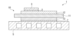
- FIG. 1 is a schematic explanatory diagram of a power module using an insulating circuit board according to an embodiment of the present invention.
- FIG. 13 is an explanatory diagram of a KAM value.
- 4 is a photograph showing the structure of a circuit layer and a metal layer of an insulating circuit board according to an embodiment of the present invention.
- FIG. 2 is a flow diagram of a method for manufacturing an insulating circuit board according to an embodiment of the present invention.
- 1A to 1C are schematic explanatory diagrams of a method for producing an insulating circuit board according to an embodiment of the present invention.
- 1 is a graph showing an example of the results of measuring the nanoindentation hardness of a circuit layer and a metal layer of an insulating circuit board in an example.
- the copper/ceramic bonded body according to an embodiment of the present invention is an insulated circuit board 10 formed by bonding a ceramic substrate 11 as a ceramic member made of ceramics to a copper plate 22 (circuit layer 12) and a copper plate 23 (metal layer 13) as copper members made of copper or a copper alloy.
- Figure 1 shows a power module 1 equipped with an insulated circuit board 10 according to this embodiment.
- This power module 1 includes an insulating circuit board 10 on which a circuit layer 12 and a metal layer 13 are arranged, a semiconductor element 3 bonded to one surface of the circuit layer 12 (the upper surface in FIG. 1) via a bonding layer 2, and a heat sink 5 disposed on the other side of the metal layer 13 (the lower side in FIG. 1).
- the semiconductor element 3 is made of a semiconductor material such as Si.
- the semiconductor element 3 and the circuit layer 12 are bonded to each other via a bonding layer 2.
- the bonding layer 2 is made of, for example, a Sn--Ag based, Sn--In based, or Sn--Ag--Cu based solder material.
- the heat sink 5 is for dissipating heat from the insulating circuit board 10.
- the heat sink 5 is made of copper or a copper alloy, and in this embodiment, is made of phosphorus deoxidized copper.
- the heat sink 5 is provided with a flow path for a cooling fluid to flow.
- the heat sink 5 and the metal layer 13 are joined by a solder layer 7 made of a solder material.
- the solder layer 7 is made of, for example, a Sn-Ag based, Sn-In based, or Sn-Ag-Cu based solder material.
- the insulating circuit board 10 of this embodiment includes a ceramic substrate 11, a circuit layer 12 disposed on one surface (the upper surface in FIG. 1) of the ceramic substrate 11, and a metal layer 13 disposed on the other surface (the lower surface in FIG. 1) of the ceramic substrate 11.
- the ceramic substrate 11 is made of ceramics such as silicon nitride ( Si3N4 ) and aluminum nitride (AlN) that have excellent insulating and heat dissipating properties.
- the ceramic substrate 11 is made of silicon nitride ( Si3N4 ), which has particularly excellent heat dissipating properties.
- the thickness of the ceramic substrate 11 is set, for example, within a range of 0.2 mm to 1.5 mm, and is set to 0.32 mm in this embodiment.
- the circuit layer 12 is formed by bonding a copper plate 22 to one surface (the upper surface in FIG. 5) of the ceramic substrate 11.
- a circuit pattern is formed on this circuit layer 12, and one surface (the upper surface in FIG. 1) serves as a mounting surface on which the semiconductor element 3 is mounted.
- the thickness of the copper plate 22 that becomes the circuit layer 12 is set within a range of 0.1 mm to 2.0 mm, and is set to 0.8 mm in this embodiment.
- the metal layer 13 is formed by joining a copper plate 23 to the other surface (the lower surface in FIG. 5) of the ceramic substrate 11.
- This metal layer 13 has the function of efficiently transferring heat from the semiconductor element 3 to the heat sink 5.
- the thickness of the copper plate 23 that becomes the metal layer 13 is set within a range of 0.1 mm to 2.0 mm, and is set to 0.8 mm in this embodiment.
- the circuit layer 12 and the metal layer 13 are made of pure copper material with a Cu content of 99.96 mass% or more, and after performing 3,000 cycles of a thermal cycle test in a liquid bath (Galden liquid) in which one cycle is held at -65°C for 5 minutes and 150°C for 5 minutes, a cross section along the thickness direction of the copper member is observed, and the ratio C/D of the proportion C of the KAM value of 0.25° or less in the measurement field centered on the grain boundary triple junction to the proportion D of the KAM value of 0.25° or less within the grain is within the range of 0.93 to 1.05.
- the KAM (Kernel Average Misorientation) value measured by EBSD is a value calculated by averaging the misorientation between one pixel and the pixels surrounding it, as shown in Fig. 2. Since the shape of a pixel is a regular hexagon, when the degree of proximity is set to 1, the average misorientation between six adjacent pixels is calculated as the KAM value. Using the KAM value, it is possible to visualize the distribution of local misorientation, i.e., strain. In FIG. 2, the KAM value at the measurement point MP is calculated by the following formula.
- the ratio C/D of the proportion C of the KAM value of 0.25° or less in a measurement field of view centered on the grain boundary triple junction to the proportion D of the KAM value of 0.25° or less within the grain is within the range of 0.93 to 1.05, so that the circuit layer 12 (copper plate 22) and the metal layer 13 (copper plate 23) are made of pure copper material with a Cu content of 99.96 mass% or more, and even when subjected to a thermal cycle load, strain is not unevenly distributed at the crystal grain boundaries.
- the nanoindentation hardness of the circuit layer 12 and the metal layer 13 at a position 100 ⁇ m away from the bonding interface with the ceramic substrate 11 is within a range of 0.40 GPa or more and 1.03 GPa or less.
- the circuit layer 12 (copper plate 22) and the metal layer 13 (copper plate 23) preferably contain one or more group A elements selected from Ca, Ba, Sr, Zr, Hf, Y, Sc, La, Ce, Pr, Nd, Pm, Sm, Eu, Gd, Tb, Dy, Ho, Er, Tm, Yb, and Lu, and one or more group B elements selected from O, S, Se, and Te in a total amount within the range of 10 ppm by mass or more and 300 ppm by mass or less.
- group A elements selected from Ca, Ba, Sr, Zr, Hf, Y, Sc, La, Ce, Pr, Nd, Pm, Sm, Eu, Gd, Tb, Dy, Ho, Er, Tm, Yb, and Lu
- group B elements selected from O, S, Se, and Te in a total amount within the range of 10 ppm by mass or more and 300 ppm by mass or less.
- compound particles 18 containing Cu and either one or both of one or more group A elements selected from Ca, Ba, Sr, Zr, Hf, Y, Sc, La, Ce, Pr, Nd, Pm, Sm, Eu, Gd, Tb, Dy, Ho, Er, Tm, Yb, and Lu, and one or more group B elements selected from O, S, Se, and Te are precipitated on the circuit layer 12 (copper plate 22) and the metal layer 13 (copper plate 23).
- the average crystal grain size in the cross section along the thickness direction of the circuit layer 12 and metal layer 13 is 100 ⁇ m or less.
- the power module 1 using the insulating circuit board 10 according to the present embodiment is used in a high-temperature environment such as an engine room, and may be subjected to severe thermal cycles. When strain accumulates at the grain boundaries during a thermal cycle test, the structure hardens, and eventually the stress caused by the thermal cycle test cannot be relieved, causing the interface between the copper and the ceramic to break.
- the ratio C/D of the proportion C of the KAM value of 0.25° or less in the measurement field centered on the grain boundary triple junction after the thermal cycle test to the proportion D of the KAM value of 0.25° or less within the grains is set within a range of 0.93 to 1.05. Therefore, even after 3000 cycles of a severe thermal cycle test in which one cycle is held at -65°C for 5 minutes and 150°C for 5 minutes in a liquid bath (Galden liquid), strain is not unevenly distributed at the grain boundaries.
- the ratio C/D of the proportion C of the KAM value of 0.25° or less in the measurement field of view centered on the grain boundary triple junction after the above-mentioned thermal cycle test to the proportion D of the KAM value of 0.25° or less in the grain is preferably 0.93 or more, more preferably 0.98 or more.
- the ratio C/D is not particularly limited, but is preferably 1.00 or less, and is about 1.05 or less even when errors due to the field of view, etc. are taken into account.
- the nanoindentation hardness of the circuit layer 12 and the metal layer 13 at a position 100 ⁇ m away from the bonding interface with the ceramic substrate 11 is preferably within a range of 0.40 GPa to 1.03 GPa.
- the lower limit of the nanoindentation hardness is preferably 0.60 GPa or more, and even more preferably 0.70 GPa or more.
- the purity of Cu in the circuit layer 12 (copper plate 22) and the metal layer 13 (copper plate 23) is specified to be 99.96 mass % or more.
- the purity of Cu is preferably 99.965 mass% or more, more preferably 99.97 mass% or more.
- the purity of Cu in the circuit layer 12 (copper plate 22) and the metal layer 13 (copper plate 23) is 99.96 mass % or more, elements such as Mg may be contained in addition to the group A elements and group B elements.
- Total content of either or both of group A elements and group B elements 10 mass ppm or more and 300 mass ppm or less
- the A group elements Ca, Ba, Sr, Zr, Hf, Y, Sc, La, Ce, Pr, Nd, Pm, Sm, Eu, Gd, Tb, Dy, Ho, Er, Tm, Yb, Lu
- the B group elements O, S, Se, Te
- the compound particles 18 are stable at high temperatures, it is possible to suppress the movement of crystal grain boundaries at high temperatures and suppress the growth of crystal grains during thermal cycle loading. In addition, since the compound particles 18 are present, the crystal structure is less changed even after thermal cycle loading, and a more uniform crystal structure can be obtained. On the other hand, if a large amount of either or both of the A group elements and the B group elements are contained, the possibility of contamination of the furnace surroundings increases, which may adversely affect manufacturability.
- the total content thereof is preferably within the range of 10 ppm by mass or more and 300 ppm by mass or less.
- the total content of either or both of the A group elements and the B group elements is more preferably 15 mass ppm or more, and even more preferably 20 mass ppm or more.
- the total content of either or both of the A group elements and the B group elements is more preferably 290 mass ppm or less, and even more preferably 280 mass ppm or less.
- the compound particles 18 containing Cu and either or both of the A group element and the B group element have high stability at high temperatures, and therefore, during thermal cycle loading, the pinning effect of the compound particles 18 can sufficiently suppress the growth of crystal grains.
- the ratio A/B of the total content A ppm of the A group elements to the total content B ppm of the B group elements is set to more than 1.0, the reaction between the A group elements and the B group elements can be suppressed, and a compound consisting of either or both of the A group elements and the B group elements and Cu can be reliably formed, and the pinning effect of the compound makes it possible to more reliably suppress the growth of crystal grains during heat treatment.
- the power module 1 using the insulating circuit board 10 of this embodiment is used in a high-temperature environment such as an engine room, and may be subjected to severe thermal cycles. Even after 3000 cycles of severe thermal cycle testing in a liquid bath (Galden liquid), in which one cycle is held at -65°C for 5 minutes and then at 150°C for 5 minutes, if the average crystal grain size is 100 ⁇ m or less, coarsening of the crystal grains after the thermal cycle load is suppressed.
- the average crystal grain size after 3000 cycles of the above-mentioned heat cycle test is preferably 90 ⁇ m or less, more preferably 80 ⁇ m or less. Also, the smaller the average crystal grain size after 3000 cycles of the above-mentioned heat cycle test, the more desirable it is, but it may be 30 ⁇ m or more or 50 ⁇ m or more.
- the bonding material 25 may be, for example, a bonding material containing Ag and active metals (Ti, Zr, Nb, Hf), that is, an Ag--Ti based brazing material (specifically, Ag--Cu--Ti material).
- the laminated copper plate 22, bonding material 25, ceramic substrate 11, bonding material 25, and copper plate 23 are pressed in the lamination direction and heated in a vacuum furnace to bond the copper plate 22, ceramic substrate 11, and copper plate 23 together.
- the temperature conditions and the like in the bonding step S03 are appropriately set depending on the bonding material 25 used.
- the pressure load P in the joining step S03 is preferably set to a range of 0.098 MPa or more and 1.47 MPa or less.
- the insulating circuit board 10 of this embodiment is manufactured through the bonding material disposing process S01, the laminating process S02, and the bonding process S03.
- Heat sink bonding process S04 Next, the heat sink 5 is joined to the other surface side of the metal layer 13 of the insulating circuit board 10 .
- the insulating circuit board 10 and the heat sink 5 are laminated with a solder material interposed therebetween and then loaded into a heating furnace, where the insulating circuit board 10 and the heat sink 5 are solder-joined to each other via the solder layer 7 .
- semiconductor element bonding step S05 Next, the semiconductor element 3 is joined to one surface of the circuit layer 12 of the insulating circuit board 10 by soldering. Through the above-described steps, the power module 1 shown in FIG. 1 is manufactured.
- the Cu content in the circuit layer 12 and the metal layer 13 is 99.96 mass % or more, and therefore the electrical conductivity and thermal conductivity of the circuit layer 12 and the metal layer 13 are particularly excellent.
- the ratio C/D of the proportion C of KAM values of 0.25° or less in a measurement field centered on the grain boundary triple junction to the proportion D of KAM values of 0.25° or less within the grains is within the range of 0.93 to 1.05. Therefore, even when subjected to severe thermal cycles, strain does not segregate at the grain boundaries, and hardening and deformation of the circuit layer 12 and the metal layer 13 can be suppressed.
- the insulating circuit board 10 of this embodiment if the nanoindentation hardness at a position 100 ⁇ m away from the bonding interface of the circuit layer 12 and metal layer 13 with the ceramic substrate 11 is within the range of 0.40 GPa to 1.03 GPa, the bonding interface of the circuit layer 12 and metal layer 13 with the ceramic substrate is not hardened more than necessary, the occurrence of cracks during thermal cycle loading can be suppressed, and the bonding reliability between the circuit layer 12 and metal layer 13 and the ceramic substrate 11 can be further improved.
- the circuit layer 12 and the metal layer 13 contain one or more group A elements selected from Ca, Ba, Sr, Zr, Hf, Y, Sc, La, Ce, Pr, Nd, Pm, Sm, Eu, Gd, Tb, Dy, Ho, Er, Tm, Yb, and Lu, and one or more group B elements selected from O, S, Se, and Te in a total amount of 10 mass ppm to 300 mass ppm, crystal growth is suppressed, coarsening of crystal grains and non-uniform crystal growth do not occur, uneven distribution of distortion is suppressed, and hardening and deformation of the circuit layer 12 and the metal layer 13 can be reliably suppressed even when subjected to a thermal cycle.
- group A elements selected from Ca, Ba, Sr, Zr, Hf, Y, Sc, La, Ce, Pr, Nd, Pm, Sm, Eu, Gd, Tb, Dy, Ho, Er, Tm, Yb, and Lu
- group B elements selected from O, S, Se
- the growth of crystal grains can be suppressed even when a thermal cycle is applied, and the crystal grains do not become coarse or the crystals do not grow unevenly.
- the uneven distribution of distortion is suppressed, and the hardening and deformation of the copper plate can be reliably suppressed.
- a power module is configured by mounting a semiconductor element on an insulating circuit board, but the present invention is not limited to this.
- an LED module may be configured by mounting an LED element on a circuit layer of an insulating circuit board, or a thermoelectric module may be configured by mounting a thermoelectric element on a circuit layer of an insulating circuit board.
- the ceramic substrate is described as being made of silicon nitride (Si 3 N 4 ), but the ceramic substrate is not limited to this, and other ceramic substrates such as aluminum nitride (AlN) and alumina (Al 2 O 3 ) may also be used.
- the circuit layer is described as being formed by bonding a copper plate to a ceramic substrate, but this is not limited to this, and the circuit layer may be formed by bonding copper pieces punched out of a copper plate to a ceramic substrate in a state in which the copper pieces are arranged in a circuit pattern. Also, the circuit pattern may be formed by etching.
- a ceramic substrate 40 mm ⁇ 40 mm ⁇ 0.32 mm thick
- silicon nitride silicon nitride
- copper plates 37 mm ⁇ 37 mm ⁇ 0.8 mm thick
- a copper plate 37 mm ⁇ 37 mm ⁇ 0.8 mm thick
- a copper plate made of commercially available oxygen-free copper was used.
- a bonding material containing Ag powder and active metal powder was applied to both sides of the ceramic substrate to a thickness of about 15 ⁇ m. Ti was selected as the active metal. The amount of each metal powder in the paste was 94 mass% Ag and 6 mass% Ti.
- the copper plate and the ceramic substrate were laminated and bonded by holding them in a vacuum at a temperature of 780° C. or higher and lower than 900° C. for 30 minutes under a pressure of 0.6 MPa. In this manner, insulating circuit boards (copper/ceramic bonded bodies) of the present invention and comparative examples were produced.
- the obtained insulating circuit board (copper/ceramic bonded body) was subjected to 3000 thermal cycles in a liquid bath (Galden liquid) under the conditions of -65°C x 5 min ⁇ -> 150°C x 5 min.
- the KAM value in the measurement field of view centered on the grain boundary triple junction after the thermal cycle test was measured, and the ratio C/D of the proportion C of the KAM value of 0.25° or less to the proportion D of the KAM value of 0.25° or less in the grain was calculated.
- the evaluation results are shown in Table 1.
- the average crystal grain size in the cross section along the thickness direction of the copper plate was measured before and after the above-mentioned thermal cycle test.
- the evaluation results are shown in Table 1.
- the average crystal grain size was measured as follows. The obtained insulating circuit board was cut in the lamination direction, and the cut surface was mechanically polished using waterproof abrasive paper and diamond abrasive grains, and then finished polished using a colloidal silica solution.
- a grain boundary map was created using high-angle grain boundaries, and in accordance with the cutting method of JIS H 0501, five line segments of predetermined lengths were drawn vertically and horizontally on the grain boundary map, the number of crystal grains that were completely cut was counted, and the average value of the cut lengths was recorded as the crystal grain size.
- the obtained insulating circuit board (copper/ceramic bonded body) was cut in the lamination direction, and the indentation hardness was measured at 5 points in one visual field and 5 points in five visual fields at positions 100 ⁇ m from the bonding surface of the ceramic substrate toward the circuit layer and metal layer at the bonding interfaces of the ceramic substrate and the circuit layer and metal layer, respectively, for a total of 50 points, and the average value was calculated.
- the evaluation results are shown in Table 1.
- FIG. 6 shows an example of the results of measuring the nanoindentation hardness of the circuit layer 12 and the metal layer 13 according to this embodiment.
- the obtained insulating circuit board was cut in the lamination direction, and then the cross section at the center in the width direction of the board was observed using a scanning electron microscope (GeminiSEM 500 manufactured by Carl Zeiss) at a magnification of 5000 times and an acceleration voltage of 5.0 kV, in a region (17 ⁇ m ⁇ 23 ⁇ m) including the bonding interface between the copper plate and the ceramic substrate.
- a scanning electron microscope GeminiSEM 500 manufactured by Carl Zeiss
- an SEM image and an element map of one or more A group elements selected from Ca, Ba, Sr, Zr, Hf, Y, Sc, La, Ce, Pr, Nd, Pm, Sm, Eu, Gd, Tb, Dy, Ho, Er, Tm, Yb, and Lu, and one or more B group elements selected from O, S, Se, and Te were obtained, and when a granular region was observed in the SEM image and Cu and an A group element or a B group element coexisted in this region, the compound particles were evaluated as "present".
- the evaluation results are shown in Table 1.
- the ratio C/D of the proportion C of KAM values of 0.25° or less in a measurement field centered on the grain boundary triple junction to the proportion D of KAM values of 0.25° or less within the grains was within the range of 0.93 to 1.05. Furthermore, in the examples of the present invention, as in the comparative example (commercially available oxygen-free copper), it was confirmed that the hardness decreased with increasing distance from the bonding interface with the ceramic substrate, and showed a sufficiently low value at a position 100 ⁇ m away from the bonding interface with the ceramic substrate. In the examples of the present invention, the bonding rate was high even after the thermal cycles were performed, and the thermal cycle reliability was excellent.
- the present invention can provide an insulated circuit board (copper/ceramic bonded body) that has excellent bonding between a ceramic substrate (ceramic member) and a copper plate (copper member) and has excellent thermal cycle reliability, even when subjected to severe thermal cycles.
- the present invention makes it possible to provide a copper/ceramic bonded body that has excellent bonding strength between a ceramic member and a copper member and excellent thermal cycle reliability, even when subjected to severe thermal cycles.
- Insulated circuit board (copper/ceramic bonded body) 11 Ceramic substrate (ceramic member) 12 Circuit layer (copper member) 13 Metal layer (copper member) 18 Compound particle MP measurement point
Landscapes
- Chemical & Material Sciences (AREA)
- Engineering & Computer Science (AREA)
- Organic Chemistry (AREA)
- Materials Engineering (AREA)
- Microelectronics & Electronic Packaging (AREA)
- Ceramic Engineering (AREA)
- Thermal Sciences (AREA)
- Physics & Mathematics (AREA)
- Crystallography & Structural Chemistry (AREA)
- Mechanical Engineering (AREA)
- Metallurgy (AREA)
- Structural Engineering (AREA)
- Ceramic Products (AREA)
Abstract
銅部材(12、13)と、セラミックス部材(11)とが接合されてなる銅/セラミックス接合体(10)であって、前記銅部材は、Cuの含有量が99.96mass%以上とされており、液槽にて-65℃で5分保持と150℃で5分保持を1サイクルとする熱サイクル試験を3000サイクル実施後において、前記銅部材の厚さ方向に沿った断面を観察し、粒界三重点を中心に配置した測定視野におけるKAM値が0.25°以下の割合Cと、粒内におけるKAM値が0.25°以下の割合Dとの比C/Dが0.93以上1.05以下の範囲内である銅/セラミックス接合体。
Description
この発明は、銅部材と、セラミックス部材とが接合されてなる銅/セラミックス接合体、および、セラミックス基板の表面に銅板が接合されてなる絶縁回路基板に関するものである。
本願は、2023年10月6日に日本に出願された特願2023-174525号及び2024年9月24日に日本に出願された特願2024-165171に基づき優先権を主張し、その内容をここに援用する。
本願は、2023年10月6日に日本に出願された特願2023-174525号及び2024年9月24日に日本に出願された特願2024-165171に基づき優先権を主張し、その内容をここに援用する。
パワーモジュール、LEDモジュールおよび熱電モジュールにおいては、絶縁層の一方の面に導電材料からなる回路層を形成した絶縁回路基板に、パワー半導体素子、LED素子および熱電素子が接合された構造とされている。
例えば、風力発電、電気自動車、ハイブリッド自動車等を制御するために用いられる大電力制御用のパワー半導体素子は、動作時の発熱量が多いことから、これを搭載する基板としては、セラミックス基板と、このセラミックス基板の一方の面に導電性の優れた金属板を接合して形成した回路層と、セラミックス基板の他方の面に金属板を接合して形成した放熱用の金属層と、を備えた絶縁回路基板が、従来から広く用いられている。
例えば、風力発電、電気自動車、ハイブリッド自動車等を制御するために用いられる大電力制御用のパワー半導体素子は、動作時の発熱量が多いことから、これを搭載する基板としては、セラミックス基板と、このセラミックス基板の一方の面に導電性の優れた金属板を接合して形成した回路層と、セラミックス基板の他方の面に金属板を接合して形成した放熱用の金属層と、を備えた絶縁回路基板が、従来から広く用いられている。
例えば、特許文献1には、セラミックス基板の一方の面および他方の面に、銅板を接合することにより回路層および金属層を形成した絶縁回路基板が提案されている。この特許文献1においては、セラミックス基板の一方の面および他方の面に、Ag-Cu-Ti系ろう材を介在させて銅板を配置し、加熱処理を行うことにより銅板が接合されている(いわゆる活性金属ろう付け法)。この活性金属ろう付け法では、活性金属であるTiが含有されたろう材を用いているため、溶融したろう材とセラミックス基板との濡れ性が向上し、セラミックス基板と銅板とが良好に接合されることになる。
ここで、回路層には半導体素子が接合されるとともに、金属層にはヒートシンク等が接合される。
ここで、回路層には半導体素子が接合されるとともに、金属層にはヒートシンク等が接合される。
ところで、最近では、絶縁回路基板に搭載される半導体素子の発熱温度が高くなる傾向にあるとともに、大電流用途で使用されることがある。このため、回路層および金属層を構成する銅材として、電気伝導性および熱伝導性に特に優れた純銅材を用いることが考えられる。
しかしながら、純銅材は、熱処理を行った際に、容易に結晶粒が粗大化するとともに、結晶粒径が大きくばらつくことになる。
しかしながら、純銅材は、熱処理を行った際に、容易に結晶粒が粗大化するとともに、結晶粒径が大きくばらつくことになる。
ここで、絶縁回路基板においては、厳しい熱サイクルが負荷されることがあり、回路層および金属層において結晶粒の粗大化や不均一な結晶成長が発生し、回路層および金属層の内部(特に結晶粒界)にひずみが偏在することになる。このように、回路層および金属層においてひずみが偏在することで、回路層および金属層の内部の降伏応力が不均一となり、回路層および金属層の硬化や変形が生じ、回路層および金属層とセラミックス部材との接合信頼性が低下するおそれがあった。また、回路層および金属層に他の部材(半導体素子、ヒートシンク等)を接合する場合には、回路層および金属層と他の部材との接合信頼性が低下するおそれがあった。
この発明は、前述した事情に鑑みてなされたものであって、厳しい冷熱サイクルを負荷した場合であっても、セラミックス部材と銅部材との接合性に優れ、冷熱サイクル信頼性に優れた銅/セラミックス接合体、および、この銅/セラミックス接合体からなる絶縁回路基板を提供することを目的とする。
前述の課題を解決するために、本発明の態様1の銅/セラミックス接合体は、銅部材と、セラミックス部材とが接合されてなる銅/セラミックス接合体であって、前記銅部材は、Cuの含有量が99.96mass%以上とされており、液槽(ガルデン液)にて-65℃で5分保持と150℃で5分保持を1サイクルとする熱サイクル試験を3000サイクル実施後において、前記銅部材の厚さ方向に沿った断面を観察し、粒界三重点を中心に配置した測定視野におけるKAM値が0.25°以下の割合Cと、粒内におけるKAM値が0.25°以下の割合Dとの比C/Dが0.93以上1.05以下の範囲内であることを特徴としている。
本発明の態様1の銅/セラミックス接合体においては、前記銅部材におけるCuの含有量が99.96mass%以上とされているので、銅部材の電気伝導性および熱伝導性に特に優れている。
そして、液槽(ガルデン液)にて-65℃で5分保持と150℃で5分保持を1サイクルとする熱サイクル試験を3000サイクル実施後において、粒界三重点を中心に配置した測定視野におけるKAM値が0.25°以下の割合Cと、粒内におけるKAM値が0.25°以下の割合Dとの比C/Dが0.93以上1.05以下の範囲内とされているので、厳しい熱サイクルを負荷しても、結晶粒界にひずみが偏析しておらず、前記銅部材の硬化や変形を抑制できる。
そして、液槽(ガルデン液)にて-65℃で5分保持と150℃で5分保持を1サイクルとする熱サイクル試験を3000サイクル実施後において、粒界三重点を中心に配置した測定視野におけるKAM値が0.25°以下の割合Cと、粒内におけるKAM値が0.25°以下の割合Dとの比C/Dが0.93以上1.05以下の範囲内とされているので、厳しい熱サイクルを負荷しても、結晶粒界にひずみが偏析しておらず、前記銅部材の硬化や変形を抑制できる。
本発明の態様2の銅/セラミックス接合体は、態様1の銅/セラミックス接合体において、前記銅部材において、前記セラミックス部材との接合界面から100μm離間した位置におけるナノインデンテーション硬度が0.40GPa以上1.03GPa以下の範囲内であることを特徴としている。
本発明の態様2の銅/セラミックス接合体によれば、前記セラミックス部材との接合界面から100μm離間した位置におけるナノインデンテーション硬度が0.40GPa以上1.03GPa以下の範囲内とされているので、銅部材のセラミックス部材との接合界面が必要以上の硬化することがなく、銅部材とセラミックス部材との接合信頼性をさらに向上させることができる。
本発明の態様2の銅/セラミックス接合体によれば、前記セラミックス部材との接合界面から100μm離間した位置におけるナノインデンテーション硬度が0.40GPa以上1.03GPa以下の範囲内とされているので、銅部材のセラミックス部材との接合界面が必要以上の硬化することがなく、銅部材とセラミックス部材との接合信頼性をさらに向上させることができる。
本発明の態様3の銅/セラミックス接合体は、態様1または態様2の銅/セラミックス接合体において、前記銅部材は、Ca,Ba,Sr,Zr,Hf,Y,Sc,La,Ce,Pr,Nd,Pm,Sm,Eu,Gd,Tb,Dy,Ho,Er,Tm,Yb,Luから選択される1種又は2種以上のA群元素、および、O,S,Se,Teから選択される1種又は2種以上のB群元素のいずれか一方又は両方を合計量で10massppm以上300massppm以下の範囲内で含有していることを特徴としている。
本発明の態様3の銅/セラミックス接合体によれば、前記銅部材が上述のA群元素およびB群元素のいずれか一方又は両方を合計量で10massppm以上300massppm以下の範囲内で含有しているので、熱サイクルを負荷しても、結晶の成長が抑制され、結晶粒の粗大化や不均一な結晶成長が生じず、ひずみが偏在することが抑制され、前記銅部材の硬化や変形を確実に抑制できる。
本発明の態様3の銅/セラミックス接合体によれば、前記銅部材が上述のA群元素およびB群元素のいずれか一方又は両方を合計量で10massppm以上300massppm以下の範囲内で含有しているので、熱サイクルを負荷しても、結晶の成長が抑制され、結晶粒の粗大化や不均一な結晶成長が生じず、ひずみが偏在することが抑制され、前記銅部材の硬化や変形を確実に抑制できる。
本発明の態様4の銅/セラミックス接合体は、態様3の銅/セラミックス接合体において、前記銅部材に、Cuと、前記A群元素および前記B群元素のいずれか一方または両方と、を含む化合物粒子が析出していることを特徴としている。
本発明の態様4の銅/セラミックス接合体によれば、Cuと、前記A群元素及び前記B群元素のいずれか一方または両方と、を含む化合物粒子が析出しているので、熱サイクルを負荷しても、結晶粒の成長を抑制でき、結晶粒の粗大化や不均一な結晶成長が生じず、ひずみが偏在することが抑制され、前記銅部材の硬化や変形を確実に抑制できる。
本発明の態様4の銅/セラミックス接合体によれば、Cuと、前記A群元素及び前記B群元素のいずれか一方または両方と、を含む化合物粒子が析出しているので、熱サイクルを負荷しても、結晶粒の成長を抑制でき、結晶粒の粗大化や不均一な結晶成長が生じず、ひずみが偏在することが抑制され、前記銅部材の硬化や変形を確実に抑制できる。
本発明の態様5の絶縁回路基板は、セラミックス基板の表面に、銅板が接合されてなる絶縁回路基板であって、前記銅板は、Cuの含有量が99.96mass%以上とされており、液槽(ガルデン液)にて-65℃で5分保持と150℃で5分保持を1サイクルとする熱サイクル試験を3000サイクル実施後において、前記銅板の厚さ方向に沿った断面を観察し、粒界三重点を中心に配置した測定視野におけるKAM値が0.25°以下の割合Cと、粒内におけるKAM値が0.25°以下の割合Dとの比C/Dが0.93以上1.05以下の範囲内であることを特徴としている。
本発明の態様5の絶縁回路基板においては、前記銅板におけるCuの含有量が99.96mass%以上とされているので、前記銅板の電気伝導性および熱伝導性に特に優れている。
そして、液槽(ガルデン液)にて-65℃で5分保持と150℃で5分保持を1サイクルとする熱サイクル試験を3000サイクル実施後において、粒界三重点を中心に配置した測定視野におけるKAM値が0.25°以下の割合Cと、粒内におけるKAM値が0.25°以下の割合Dとの比C/Dが0.93以上1.05以下の範囲内とされているので、厳しい熱サイクルを負荷しても、結晶粒界にひずみが偏析しておらず、前記銅板の硬化や変形を抑制できる。
そして、液槽(ガルデン液)にて-65℃で5分保持と150℃で5分保持を1サイクルとする熱サイクル試験を3000サイクル実施後において、粒界三重点を中心に配置した測定視野におけるKAM値が0.25°以下の割合Cと、粒内におけるKAM値が0.25°以下の割合Dとの比C/Dが0.93以上1.05以下の範囲内とされているので、厳しい熱サイクルを負荷しても、結晶粒界にひずみが偏析しておらず、前記銅板の硬化や変形を抑制できる。
本発明の態様6の絶縁回路基板は、態様5の絶縁回路基板において、前記銅板において、前記セラミックス基板との接合界面から100μm離間した位置におけるナノインデンテーション硬度が0.40GPa以上1.03GPa以下の範囲内であることを特徴としている。
本発明の態様6の絶縁回路基板によれば、前記セラミックス基板との接合界面から100μm離間した位置におけるナノインデンテーション硬度が0.40GPa以上1.03GPa以下の範囲内とされているので、銅板のセラミックス基板との接合界面が必要以上の硬化することがなく、銅板とセラミックス基板との接合信頼性をさらに向上させることができる。
本発明の態様6の絶縁回路基板によれば、前記セラミックス基板との接合界面から100μm離間した位置におけるナノインデンテーション硬度が0.40GPa以上1.03GPa以下の範囲内とされているので、銅板のセラミックス基板との接合界面が必要以上の硬化することがなく、銅板とセラミックス基板との接合信頼性をさらに向上させることができる。
本発明の態様7の絶縁回路基板は、態様5または態様6の絶縁回路基板において、前記銅部材は、Ca,Ba,Sr,Zr,Hf,Y,Sc,La,Ce,Pr,前記銅板は、Ca,Ba,Sr,Zr,Hf,Y,Sc,La,Ce,Pr,Nd,Pm,Sm,Eu,Gd,Tb,Dy,Ho,Er,Tm,Yb,Luから選択される1種又は2種以上のA群元素、および、O,S,Se,Teから選択される1種又は2種以上のB群元素のいずれか一方又は両方を合計量で10massppm以上300massppm以下の範囲内で含有していることを特徴としている。
本発明の態様7の絶縁回路基板によれば、前記銅板が上述のA群元素およびB群元素のいずれか一方又は両方を合計量で10massppm以上300massppm以下の範囲内で含有しているので、熱サイクルを負荷しても、結晶の成長が抑制され、結晶粒の粗大化や不均一な結晶成長が生じず、ひずみが偏在することが抑制され、前記銅板の硬化や変形を確実に抑制できる。
本発明の態様7の絶縁回路基板によれば、前記銅板が上述のA群元素およびB群元素のいずれか一方又は両方を合計量で10massppm以上300massppm以下の範囲内で含有しているので、熱サイクルを負荷しても、結晶の成長が抑制され、結晶粒の粗大化や不均一な結晶成長が生じず、ひずみが偏在することが抑制され、前記銅板の硬化や変形を確実に抑制できる。
本発明の態様8の絶縁回路基板は、態様7の絶縁回路基板において、前記銅板に、Cuと、前記A群元素および前記B群元素のいずれか一方または両方と、を含む化合物粒子が析出していることを特徴としている。
本発明の態様8の絶縁回路基板によれば、前記銅板に、Cuと、前記A群元素および前記B群元素のいずれか一方または両方と、を含む化合物粒子が析出しているので、熱サイクルを負荷しても、結晶粒の成長を抑制でき、結晶粒の粗大化や不均一な結晶成長が生じず、ひずみが偏在することが抑制され、前記銅板の硬化や変形を確実に抑制できる。
本発明の態様8の絶縁回路基板によれば、前記銅板に、Cuと、前記A群元素および前記B群元素のいずれか一方または両方と、を含む化合物粒子が析出しているので、熱サイクルを負荷しても、結晶粒の成長を抑制でき、結晶粒の粗大化や不均一な結晶成長が生じず、ひずみが偏在することが抑制され、前記銅板の硬化や変形を確実に抑制できる。
本発明によれば、厳しい冷熱サイクルを負荷した場合であっても、セラミックス部材と銅部材との接合性に優れ、冷熱サイクル信頼性に優れた銅/セラミックス接合体、および、この銅/セラミックス接合体からなる絶縁回路基板を提供することができる。
以下に、本発明の実施形態について添付した図面を参照して説明する。
本発明の実施形態に係る銅/セラミックス接合体は、セラミックスからなるセラミックス部材としてのセラミックス基板11と、銅又は銅合金からなる銅部材としての銅板22(回路層12)および銅板23(金属層13)とが接合されてなる絶縁回路基板10である。図1に、本実施形態である絶縁回路基板10を備えたパワーモジュール1を示す。
このパワーモジュール1は、回路層12および金属層13が配設された絶縁回路基板10と、回路層12の一方の面(図1において上面)に接合層2を介して接合された半導体素子3と、金属層13の他方側(図1において下側)に配置されたヒートシンク5と、を備えている。
半導体素子3は、Si等の半導体材料で構成されている。この半導体素子3と回路層12は、接合層2を介して接合されている。
接合層2は、例えばSn-Ag系、Sn-In系、若しくはSn-Ag-Cu系のはんだ材で構成されている。
接合層2は、例えばSn-Ag系、Sn-In系、若しくはSn-Ag-Cu系のはんだ材で構成されている。
ヒートシンク5は、前述の絶縁回路基板10からの熱を放散するためのものである。このヒートシンク5は、銅又は銅合金で構成されており、本実施形態ではりん脱酸銅で構成されている。このヒートシンク5には、冷却用の流体が流れるための流路が設けられている。
なお、本実施形態においては、ヒートシンク5と金属層13とが、はんだ材からなるはんだ層7によって接合されている。このはんだ層7は、例えばSn-Ag系、Sn-In系、若しくはSn-Ag-Cu系のはんだ材で構成されている。
なお、本実施形態においては、ヒートシンク5と金属層13とが、はんだ材からなるはんだ層7によって接合されている。このはんだ層7は、例えばSn-Ag系、Sn-In系、若しくはSn-Ag-Cu系のはんだ材で構成されている。
そして、本実施形態である絶縁回路基板10は、図1に示すように、セラミックス基板11と、このセラミックス基板11の一方の面(図1において上面)に配設された回路層12と、セラミックス基板11の他方の面(図1において下面)に配設された金属層13と、を備えている。
セラミックス基板11は、絶縁性および放熱性に優れた窒化ケイ素(Si3N4)、窒化アルミニウム(AlN)等のセラミックスで構成されている。本実施形態では、セラミックス基板11は、特に放熱性の優れた窒化ケイ素(Si3N4)で構成されている。また、セラミックス基板11の厚さは、例えば、0.2mm以上1.5mm以下の範囲内に設定されており、本実施形態では、0.32mmに設定されている。
回路層12は、図5に示すように、セラミックス基板11の一方の面(図5において上面)に銅板22が接合されることにより形成されている。この回路層12には、回路パターンが形成されており、その一方の面(図1において上面)が、半導体素子3が搭載される搭載面とされている。
なお、回路層12となる銅板22の厚さは0.1mm以上2.0mm以下の範囲内に設定されており、本実施形態では、0.8mmに設定されている。
なお、回路層12となる銅板22の厚さは0.1mm以上2.0mm以下の範囲内に設定されており、本実施形態では、0.8mmに設定されている。
金属層13は、図5に示すように、セラミックス基板11の他方の面(図5において下面)に、銅板23が接合されることにより形成されている。この金属層13は、半導体素子3からの熱をヒートシンク5へと効率良く伝達させる作用効果を有するものである。
なお、金属層13となる銅板23の厚さは0.1mm以上2.0mm以下の範囲内に設定されており、本実施形態では、0.8mmに設定されている。
なお、金属層13となる銅板23の厚さは0.1mm以上2.0mm以下の範囲内に設定されており、本実施形態では、0.8mmに設定されている。
そして、本実施形態である絶縁回路基板10においては、回路層12および金属層13は、Cuの含有量が99.96mass%以上の純銅材で構成されており、液槽(ガルデン液)にて-65℃で5分保持と150℃で5分保持を1サイクルとする熱サイクル試験を3000サイクル実施後において、前記銅部材の厚さ方向に沿った断面を観察し、粒界三重点を中心に配置した測定視野におけるKAM値が0.25°以下の割合Cと、粒内におけるKAM値が0.25°以下の割合Dとの比C/Dが0.93以上1.05以下の範囲内とされている。
ここで、EBSDにより測定されるKAM(Kernel Average Misorientation)値は、図2に示すように、1つのピクセルとそれを取り囲むピクセル間との方位差を平均値化することで算出される値である。ピクセルの形状は正六角形のため、近接次数を1とする場合、隣接する六つのピクセルとの方位差の平均値がKAM値として算出される。KAM値を用いることで、局所的な方位差、すなわちひずみの分布を可視化できる。
なお図2において、測定点MPのKAM値は下記式で求められる。
測定点MPのKAM値=(Aとの方位差+Bとの方位差+…Fとの方位差)/6
すなわち、本実施形態においては、粒界三重点を中心に配置した測定視野におけるKAM値が0.25°以下の割合Cと、粒内におけるKAM値が0.25°以下の割合Dとの比C/Dが0.93以上1.05以下の範囲内とされているので、回路層12(銅板22)および金属層13(銅板23)が、Cuの含有量が99.96mass%以上の純銅材であって、熱サイクル負荷時においても、結晶粒界にひずみが偏在していないことになる。
なお図2において、測定点MPのKAM値は下記式で求められる。
測定点MPのKAM値=(Aとの方位差+Bとの方位差+…Fとの方位差)/6
すなわち、本実施形態においては、粒界三重点を中心に配置した測定視野におけるKAM値が0.25°以下の割合Cと、粒内におけるKAM値が0.25°以下の割合Dとの比C/Dが0.93以上1.05以下の範囲内とされているので、回路層12(銅板22)および金属層13(銅板23)が、Cuの含有量が99.96mass%以上の純銅材であって、熱サイクル負荷時においても、結晶粒界にひずみが偏在していないことになる。
また、本実施形態である絶縁回路基板10においては、回路層12および金属層13において、セラミックス基板11との接合界面から100μm離間した位置におけるナノインデンテーション硬度が0.40GPa以上1.03GPa以下の範囲内とされていることが好ましい。
さらに、本実施形態である絶縁回路基板10においては、回路層12(銅板22)および金属層13(銅板23)は、Ca,Ba,Sr,Zr,Hf,Y,Sc,La,Ce,Pr,Nd,Pm,Sm,Eu,Gd,Tb,Dy,Ho,Er,Tm,Yb,Luから選択される1種又は2種以上のA群元素、および、O,S,Se,Teから選択される1種又は2種以上のB群元素のいずれか一方又は両方を合計量で10massppm以上300massppm以下の範囲内で含有していることが好ましい。
さらに、本実施形態である絶縁回路基板10においては、図3に示すように、回路層12(銅板22)および金属層13(銅板23)に、Cuと、Ca,Ba,Sr,Zr,Hf,Y,Sc,La,Ce,Pr,Nd,Pm,Sm,Eu,Gd,Tb,Dy,Ho,Er,Tm,Yb,Luから選択される1種又は2種以上のA群元素およびO,S,Se,Teから選択される1種又は2種以上のB群元素のいずれか一方または両方と、を含む化合物粒子18が析出していることが好ましい。
また、本実施形態である絶縁回路基板10においては、液槽(ガルデン液)にて-65℃で5分保持と150℃で5分保持を1サイクルとする熱サイクル試験を3000サイクル実施後において、セラミックス基板11に割れが確認されない。
さらに、本実施形態である絶縁回路基板10においては、液槽(ガルデン液)にて-65℃で5分保持と150℃で5分保持を1サイクルとする熱サイクル試験を3000サイクル実施後において、回路層12および金属層13の厚さ方向に沿った断面における平均結晶粒径が100μm以下とされていることが好ましい。
ここで、本実施形態である絶縁回路基板10において、上述のように、熱サイクル試験後の粒界三重点を中心に配置した測定視野におけるKAM値が0.25°以下の割合Cと、粒内におけるKAM値が0.25°以下の割合Dとの比C/D、セラミックス基板11との接合界面から100μm離間した位置におけるナノインデンテーション硬度、回路層12(銅板22)および金属層13(銅板23)の組成、化合物粒子、熱サイクル試験後のセラミックス基板11の割れの有無、熱サイクル試験後の平均結晶粒径を規定した理由について、以下に説明する。
(熱サイクル試験後の粒界三重点を中心に配置した測定視野におけるKAM値が0.25°以下の割合Cと、粒内におけるKAM値が0.25°以下の割合Dとの比C/D)
本実施形態である絶縁回路基板10を用いたパワーモジュール1においては、エンジンルーム等の高温環境下で使用され、厳しい熱サイクルが負荷されることがある。熱サイクル試験にて結晶粒界にひずみがたまると組織が硬くなり、やがて熱サイクル試験による応力の緩和ができなくなるため銅とセラミックスとの界面が破壊する。本実施形態においては、上述のように、熱サイクル試験後の粒界三重点を中心に配置した測定視野におけるKAM値が0.25°以下の割合Cと、粒内におけるKAM値が0.25°以下の割合Dとの比C/Dが0.93以上1.05以下の範囲内とされているので、液槽(ガルデン液)にて-65℃で5分保持と150℃で5分保持を1サイクルとする厳しい熱サイクル試験を3000サイクル実施後においても、結晶粒界にひずみが偏在していないことになる。
なお、上述の熱サイクル試験後の粒界三重点を中心に配置した測定視野におけるKAM値が0.25°以下の割合Cと、粒内におけるKAM値が0.25°以下の割合Dとの比C/Dは0.93以上であることが好ましく、0.98以上であることがより好ましい。また、比C/Dは特に制限ないが1.00以下であることが好ましく、視野等による誤差を加味しても1.05以下程度である。
本実施形態である絶縁回路基板10を用いたパワーモジュール1においては、エンジンルーム等の高温環境下で使用され、厳しい熱サイクルが負荷されることがある。熱サイクル試験にて結晶粒界にひずみがたまると組織が硬くなり、やがて熱サイクル試験による応力の緩和ができなくなるため銅とセラミックスとの界面が破壊する。本実施形態においては、上述のように、熱サイクル試験後の粒界三重点を中心に配置した測定視野におけるKAM値が0.25°以下の割合Cと、粒内におけるKAM値が0.25°以下の割合Dとの比C/Dが0.93以上1.05以下の範囲内とされているので、液槽(ガルデン液)にて-65℃で5分保持と150℃で5分保持を1サイクルとする厳しい熱サイクル試験を3000サイクル実施後においても、結晶粒界にひずみが偏在していないことになる。
なお、上述の熱サイクル試験後の粒界三重点を中心に配置した測定視野におけるKAM値が0.25°以下の割合Cと、粒内におけるKAM値が0.25°以下の割合Dとの比C/Dは0.93以上であることが好ましく、0.98以上であることがより好ましい。また、比C/Dは特に制限ないが1.00以下であることが好ましく、視野等による誤差を加味しても1.05以下程度である。
(ナノインデンテーション硬度)
本実施形態である絶縁回路基板10において、回路層12および金属層13のセラミックス基板11との接合界面近傍における硬度が十分に低いと、熱サイクル負荷時におけるクラックの発生を抑制することができる。
そこで、本実施形態においては、回路層12および金属層13において、セラミックス基板11との接合界面から100μm離間した位置におけるナノインデンテーション硬度が0.40GPa以上1.03GPa以下の範囲内であることが好ましい。
なお、上述のナノインデンテーション硬度は低いほど望ましく、0.90GPa以下であることがより好ましく、0.81GPa以下であることがさらに好ましい。一方、上述のナノインデンテーション硬度を必要以上に低くするためには多くのコストが必要となることから、ナノインデンテーション硬度の下限は0.60GPa以上であることが好ましく、0.70GPa以上であることがさらに好ましい。
本実施形態である絶縁回路基板10において、回路層12および金属層13のセラミックス基板11との接合界面近傍における硬度が十分に低いと、熱サイクル負荷時におけるクラックの発生を抑制することができる。
そこで、本実施形態においては、回路層12および金属層13において、セラミックス基板11との接合界面から100μm離間した位置におけるナノインデンテーション硬度が0.40GPa以上1.03GPa以下の範囲内であることが好ましい。
なお、上述のナノインデンテーション硬度は低いほど望ましく、0.90GPa以下であることがより好ましく、0.81GPa以下であることがさらに好ましい。一方、上述のナノインデンテーション硬度を必要以上に低くするためには多くのコストが必要となることから、ナノインデンテーション硬度の下限は0.60GPa以上であることが好ましく、0.70GPa以上であることがさらに好ましい。
(Cuの含有量:99.96mass%以上)
本実施形態である絶縁回路基板10の回路層12および金属層13においては、通電時の発熱を抑制するために、電気伝導性および熱伝導性に優れていることが求められる。
そこで、本実施形態においては、回路層12(銅板22)および金属層13(銅板23)におけるCuの純度を99.96mass%以上に規定している。
なお、Cuの純度は99.965mass%以上であることが好ましく、99.97mass%以上であることがさらに好ましい。また、Cuの純度の上限に特に制限はないが、99.999mass%を超える場合には、特別な精錬工程が必要となり、製造コストが大幅に増加するため、99.999mass%以下とすることが好ましい。
なお、回路層12(銅板22)および金属層13(銅板23)のCuの純度が99.96mass%以上であれば、A群元素、B群元素以外にもMgなどの元素が含まれていてもよい。
本実施形態である絶縁回路基板10の回路層12および金属層13においては、通電時の発熱を抑制するために、電気伝導性および熱伝導性に優れていることが求められる。
そこで、本実施形態においては、回路層12(銅板22)および金属層13(銅板23)におけるCuの純度を99.96mass%以上に規定している。
なお、Cuの純度は99.965mass%以上であることが好ましく、99.97mass%以上であることがさらに好ましい。また、Cuの純度の上限に特に制限はないが、99.999mass%を超える場合には、特別な精錬工程が必要となり、製造コストが大幅に増加するため、99.999mass%以下とすることが好ましい。
なお、回路層12(銅板22)および金属層13(銅板23)のCuの純度が99.96mass%以上であれば、A群元素、B群元素以外にもMgなどの元素が含まれていてもよい。
(A群元素及びB群元素のいずれか一方又は両方の合計含有量:10massppm以上300massppm以下)
本実施形態である絶縁回路基板10の回路層12および金属層13において、A群元素(Ca,Ba,Sr,Zr,Hf,Y,Sc,La,Ce,Pr,Nd,Pm,Sm,Eu,Gd,Tb,Dy,Ho,Er,Tm,Yb,Lu)およびB群元素(O,S,Se,Te)のいずれか一方又は両方を含有することにより、Cuと、前記A群元素および前記B群元素のいずれか一方または両方と、を含む化合物粒子18が形成される。この化合物粒子18は、高温で安定であることから、高温での結晶粒界の移動を抑制することができ、熱サイクル負荷時における結晶粒の成長を抑制することが可能となる。また、化合物粒子18が存在しているので、熱サイクル負荷後においても結晶組織の変化が少なく、かつ、さらに均一な結晶組織を得ることが可能となる。一方、A群元素およびB群元素のいずれか一方又は両方を多量に含有すると、炉周辺が汚染される可能性が高まり、製造性に悪影響を与えてしまうおそれがあった。
本実施形態である絶縁回路基板10の回路層12および金属層13において、A群元素(Ca,Ba,Sr,Zr,Hf,Y,Sc,La,Ce,Pr,Nd,Pm,Sm,Eu,Gd,Tb,Dy,Ho,Er,Tm,Yb,Lu)およびB群元素(O,S,Se,Te)のいずれか一方又は両方を含有することにより、Cuと、前記A群元素および前記B群元素のいずれか一方または両方と、を含む化合物粒子18が形成される。この化合物粒子18は、高温で安定であることから、高温での結晶粒界の移動を抑制することができ、熱サイクル負荷時における結晶粒の成長を抑制することが可能となる。また、化合物粒子18が存在しているので、熱サイクル負荷後においても結晶組織の変化が少なく、かつ、さらに均一な結晶組織を得ることが可能となる。一方、A群元素およびB群元素のいずれか一方又は両方を多量に含有すると、炉周辺が汚染される可能性が高まり、製造性に悪影響を与えてしまうおそれがあった。
このため、A群元素及びB群元素のいずれか一方又は両方を含有する場合には、その合計含有量を10massppm以上300massppm以下の範囲内であることが好ましい。
なお、A群元素及びB群元素のいずれか一方又は両方の合計含有量は、15massppm以上であることがより好ましく、20massppm以上であることがさらに好ましい。また、A群元素及びB群元素のいずれか一方又は両方の合計含有量は290massppm以下であることがより好ましく、280massppm以下であることがさらに好ましい。
なお、A群元素及びB群元素のいずれか一方又は両方の合計含有量は、15massppm以上であることがより好ましく、20massppm以上であることがさらに好ましい。また、A群元素及びB群元素のいずれか一方又は両方の合計含有量は290massppm以下であることがより好ましく、280massppm以下であることがさらに好ましい。
(Cuと、前記A群元素および前記B群元素のいずれか一方または両方と、を含む化合物粒子)
上述のように、Cuと、前記A群元素および前記B群元素のいずれか一方または両方と、を含む化合物粒子18は、高温での安定性が高い。このため、熱サイクル負荷時において、この化合物粒子18のピン止め効果により、結晶粒の成長を十分に抑制することが可能となる。
特に、前記A群元素の合計含有量Amassppmと前記B群元素の合計含有量Bmassppmとの比A/Bが1.0超えとされていると、A群元素とB群元素とが反応することを抑制でき、前記A群元素および前記B群元素のいずれか一方または両方とCuとからなる化合物を確実に形成することができ、化合物のピン止め効果によって、熱処理時における結晶粒の成長をさらに確実に抑制することが可能となる。
上述のように、Cuと、前記A群元素および前記B群元素のいずれか一方または両方と、を含む化合物粒子18は、高温での安定性が高い。このため、熱サイクル負荷時において、この化合物粒子18のピン止め効果により、結晶粒の成長を十分に抑制することが可能となる。
特に、前記A群元素の合計含有量Amassppmと前記B群元素の合計含有量Bmassppmとの比A/Bが1.0超えとされていると、A群元素とB群元素とが反応することを抑制でき、前記A群元素および前記B群元素のいずれか一方または両方とCuとからなる化合物を確実に形成することができ、化合物のピン止め効果によって、熱処理時における結晶粒の成長をさらに確実に抑制することが可能となる。
(冷熱サイクル試験後の基板の割れの有無)
液槽(ガルデン液)にて-65℃で5分保持と150℃で5分保持を1サイクルとする熱サイクル試験を3000サイクル実施後の絶縁回路基板について、超音波探傷装置(株式会社日立パワーソリューションズ製FineSAT200)を用いて絶縁回路基板の割れの有無を評価した。本実施形態の絶縁回路基板10(銅/セラミックス接合体)は、回路層12、金属層13、セラミックス基板11のいずれかににも割れが確認された。
一方、無酸素銅を用いた絶縁回路基板においては、銅/セラミックス界面においてセラミックス基板にわずかな割れが生じた。
液槽(ガルデン液)にて-65℃で5分保持と150℃で5分保持を1サイクルとする熱サイクル試験を3000サイクル実施後の絶縁回路基板について、超音波探傷装置(株式会社日立パワーソリューションズ製FineSAT200)を用いて絶縁回路基板の割れの有無を評価した。本実施形態の絶縁回路基板10(銅/セラミックス接合体)は、回路層12、金属層13、セラミックス基板11のいずれかににも割れが確認された。
一方、無酸素銅を用いた絶縁回路基板においては、銅/セラミックス界面においてセラミックス基板にわずかな割れが生じた。
(熱サイクル試験後の平均結晶粒径)
本実施形態である絶縁回路基板10を用いたパワーモジュール1においては、エンジンルーム等の高温環境下で使用され、厳しい熱サイクルが負荷されることがある。液槽(ガルデン液)にて-65℃で5分保持と150℃で5分保持を1サイクルとする厳しい熱サイクル試験を3000サイクル実施後においても、平均結晶粒径が100μm以下とされている場合には、熱サイクル負荷後の結晶粒の粗大化が抑制されることになる。
なお、上述の熱サイクル試験を3000サイクル実施後における平均結晶粒径は90μm以下であることが好ましく、80μm以下であることがより好ましい。また、上述の熱サイクル試験を3000サイクル実施後における平均結晶粒径は小さいほど望ましいが、30μm以上や50μm以上であってもよい。
本実施形態である絶縁回路基板10を用いたパワーモジュール1においては、エンジンルーム等の高温環境下で使用され、厳しい熱サイクルが負荷されることがある。液槽(ガルデン液)にて-65℃で5分保持と150℃で5分保持を1サイクルとする厳しい熱サイクル試験を3000サイクル実施後においても、平均結晶粒径が100μm以下とされている場合には、熱サイクル負荷後の結晶粒の粗大化が抑制されることになる。
なお、上述の熱サイクル試験を3000サイクル実施後における平均結晶粒径は90μm以下であることが好ましく、80μm以下であることがより好ましい。また、上述の熱サイクル試験を3000サイクル実施後における平均結晶粒径は小さいほど望ましいが、30μm以上や50μm以上であってもよい。
以下に、本実施形態に係る絶縁回路基板10の製造方法について、図4および図5を参照して説明する。
(接合材配設工程S01)
まず、セラミックス基板11を準備し、図5に示すように、回路層12となる銅板22とセラミックス基板11との間、および、金属層13となる銅板23とセラミックス基板11との間に、接合材25を配設する。
接合材25としては、例えば、Agと活性金属(Ti,Zr,Nb,Hf)を含有する接合材、つまり、Ag-Ti系ろう材(具体的にはAg-Cu-Ti材)等を用いることができる。
まず、セラミックス基板11を準備し、図5に示すように、回路層12となる銅板22とセラミックス基板11との間、および、金属層13となる銅板23とセラミックス基板11との間に、接合材25を配設する。
接合材25としては、例えば、Agと活性金属(Ti,Zr,Nb,Hf)を含有する接合材、つまり、Ag-Ti系ろう材(具体的にはAg-Cu-Ti材)等を用いることができる。
(積層工程S02)
次に、銅板22とセラミックス基板11を、接合材25を介して積層するとともに、セラミックス基板11と銅板23を、接合材25を介して積層する。
次に、銅板22とセラミックス基板11を、接合材25を介して積層するとともに、セラミックス基板11と銅板23を、接合材25を介して積層する。
(接合工程S03)
次に、積層された銅板22、接合材25、セラミックス基板11、接合材25、銅板23を、積層方向に加圧するとともに、真空炉内に装入して加熱し、銅板22とセラミックス基板11と銅板23を接合する。
ここで、接合工程S03における温度条件等は、用いる接合材25に応じて適宜設定することが好ましい。
なお、接合工程S03における加圧荷重Pは、0.098MPa以上1.47MPa以下の範囲内とすることが好ましい。
次に、積層された銅板22、接合材25、セラミックス基板11、接合材25、銅板23を、積層方向に加圧するとともに、真空炉内に装入して加熱し、銅板22とセラミックス基板11と銅板23を接合する。
ここで、接合工程S03における温度条件等は、用いる接合材25に応じて適宜設定することが好ましい。
なお、接合工程S03における加圧荷重Pは、0.098MPa以上1.47MPa以下の範囲内とすることが好ましい。
以上のように、接合材配設工程S01と、積層工程S02と、接合工程S03とによって、本実施形態である絶縁回路基板10が製造されることになる。
(ヒートシンク接合工程S04)
次に、絶縁回路基板10の金属層13の他方の面側にヒートシンク5を接合する。
絶縁回路基板10とヒートシンク5とを、はんだ材を介して積層して加熱炉に装入し、はんだ層7を介して絶縁回路基板10とヒートシンク5とをはんだ接合する。
次に、絶縁回路基板10の金属層13の他方の面側にヒートシンク5を接合する。
絶縁回路基板10とヒートシンク5とを、はんだ材を介して積層して加熱炉に装入し、はんだ層7を介して絶縁回路基板10とヒートシンク5とをはんだ接合する。
(半導体素子接合工程S05)
次に、絶縁回路基板10の回路層12の一方の面に、半導体素子3をはんだ付けにより接合する。
前述の工程により、図1に示すパワーモジュール1が製出される。
次に、絶縁回路基板10の回路層12の一方の面に、半導体素子3をはんだ付けにより接合する。
前述の工程により、図1に示すパワーモジュール1が製出される。
以上のような構成とされた本実施形態の絶縁回路基板10(銅/セラミックス接合体)によれば、回路層12および金属層13におけるCuの含有量が99.96mass%以上とされているので、回路層12および金属層13の電気伝導性および熱伝導性に特に優れている。
そして、液槽(ガルデン液)にて-65℃で5分保持と150℃で5分保持を1サイクルとする熱サイクル試験を3000サイクル実施後において、粒界三重点を中心に配置した測定視野におけるKAM値が0.25°以下の割合Cと、粒内におけるKAM値が0.25°以下の割合Dとの比C/Dが0.93以上1.05以下の範囲内とされているので、厳しい熱サイクルを負荷しても、結晶粒界にひずみが偏析しておらず、回路層12および金属層13の硬化や変形を抑制できる。
そして、液槽(ガルデン液)にて-65℃で5分保持と150℃で5分保持を1サイクルとする熱サイクル試験を3000サイクル実施後において、粒界三重点を中心に配置した測定視野におけるKAM値が0.25°以下の割合Cと、粒内におけるKAM値が0.25°以下の割合Dとの比C/Dが0.93以上1.05以下の範囲内とされているので、厳しい熱サイクルを負荷しても、結晶粒界にひずみが偏析しておらず、回路層12および金属層13の硬化や変形を抑制できる。
本実施形態の絶縁回路基板10において、回路層12および金属層13のセラミックス基板11との接合界面から100μm離間した位置におけるナノインデンテーション硬度が0.40GPa以上1.03GPa以下の範囲内である場合には、回路層12および金属層13のセラミックス基板との接合界面が必要以上の硬化しておらず、熱サイクル負荷時におけるクラックの発生を抑制でき、回路層12および金属層13とセラミックス基板11との接合信頼性をさらに向上させることができる。
本実施形態の絶縁回路基板10において、回路層12および金属層13が、Ca,Ba,Sr,Zr,Hf,Y,Sc,La,Ce,Pr,Nd,Pm,Sm,Eu,Gd,Tb,Dy,Ho,Er,Tm,Yb,Luから選択される1種又は2種以上のA群元素、および、O,S,Se,Teから選択される1種又は2種以上のB群元素のいずれか一方又は両方を合計量で10massppm以上300massppm以下の範囲内で含有している場合には、熱サイクルを負荷しても、結晶の成長が抑制され、結晶粒の粗大化や不均一な結晶成長が生じず、ひずみが偏在することが抑制され、回路層12および金属層13の硬化や変形を確実に抑制できる。
本実施形態の絶縁回路基板10において、回路層12および金属層13にCuと、前記A群元素および前記B群元素のいずれか一方または両方と、を含む化合物粒子18が析出している場合には、熱サイクルを負荷しても、結晶粒の成長を抑制でき、結晶粒の粗大化や不均一な結晶成長が生じず、ひずみが偏在することが抑制され、前記銅板の硬化や変形を確実に抑制できる。
以上、本発明の実施形態について説明したが、本発明はこれに限定されることはなく、その発明の技術的思想を逸脱しない範囲で適宜変更可能である。
例えば、本実施形態では、絶縁回路基板に半導体素子を搭載してパワーモジュールを構成するものとして説明したが、これに限定されることはない。例えば、絶縁回路基板の回路層にLED素子を搭載してLEDモジュールを構成してもよいし、絶縁回路基板の回路層に熱電素子を搭載して熱電モジュールを構成してもよい。
例えば、本実施形態では、絶縁回路基板に半導体素子を搭載してパワーモジュールを構成するものとして説明したが、これに限定されることはない。例えば、絶縁回路基板の回路層にLED素子を搭載してLEDモジュールを構成してもよいし、絶縁回路基板の回路層に熱電素子を搭載して熱電モジュールを構成してもよい。
また、本実施形態の絶縁回路基板では、セラミックス基板として、窒化ケイ素(Si3N4)で構成されたものを例に挙げて説明したが、これに限定されることはなく、窒化アルミニウム(AlN)、アルミナ(Al2O3)等の他のセラミックス基板を用いたものであってもよい。
さらに、本実施形態においては、回路層を、銅板をセラミックス基板に接合することにより形成するものとして説明したが、これに限定されることはなく、銅板を打ち抜いた銅片を回路パターン状に配置された状態でセラミックス基板に接合されることによって回路層を形成してもよい。また、エッチングにて回路パターンを形成してもよい。
以下に、本発明の効果を確認すべく行った確認実験の結果について説明する。
まず、窒化ケイ素からなるセラミックス基板(40mm×40mm×厚さ0.32mm)を準備した。
そして、回路層および金属層となる銅板として、本発明例においては、表1及び表2に示す組成の銅板(37mm×37mm×厚さ0.8mm)を用いた。また、比較例として、市販の無酸素銅からなる銅板(37mm×37mm×厚さ0.8mm)を用いた。
そして、回路層および金属層となる銅板として、本発明例においては、表1及び表2に示す組成の銅板(37mm×37mm×厚さ0.8mm)を用いた。また、比較例として、市販の無酸素銅からなる銅板(37mm×37mm×厚さ0.8mm)を用いた。
次に、セラミックス基板の両面にAg粉及び活性金属粉を含む接合材を厚さ15μm程度になるよう塗布した。このとき、活性金属にはTiを選択した。ペースト中の各金属粉の量は94mass%Ag、6mass%Tiとした。
次に銅板とセラミックス基板とを積層し、0.6MPaで加圧した状態で真空中にて780℃以上900℃未満の温度で30分保持し接合した。
以上のようにして、本発明例および比較例の絶縁回路基板(銅/セラミックス接合体)を作製した。
次に銅板とセラミックス基板とを積層し、0.6MPaで加圧した状態で真空中にて780℃以上900℃未満の温度で30分保持し接合した。
以上のようにして、本発明例および比較例の絶縁回路基板(銅/セラミックス接合体)を作製した。
(冷熱サイクル試験後のKAM値)
得られた絶縁回路基板(銅/セラミックス接合体)に対して、液槽(ガルデン液)にて-65℃×5min←→150℃×5minの条件で冷熱サイクルを3000サイクルまで行った。
冷熱サイクル試験後の粒界三重点を中心に配置した測定視野におけるKAM値を測定し、KAM値が0.25°以下の割合Cと、粒内におけるKAM値が0.25°以下の割合Dとの比C/Dを算出した。評価結果を表1に示す。
得られた絶縁回路基板(銅/セラミックス接合体)に対して、液槽(ガルデン液)にて-65℃×5min←→150℃×5minの条件で冷熱サイクルを3000サイクルまで行った。
冷熱サイクル試験後の粒界三重点を中心に配置した測定視野におけるKAM値を測定し、KAM値が0.25°以下の割合Cと、粒内におけるKAM値が0.25°以下の割合Dとの比C/Dを算出した。評価結果を表1に示す。
(冷熱サイクル試験後の平均結晶粒径)
上述の冷熱サイクル試験前と冷熱サイクル試験後の銅板の厚さ方向に沿った断面における平均結晶粒径を測定した。評価結果を表1に示す。
なお、平均結晶粒径は次のようにして測定した。
得られた絶縁回路基板を積層方向に切断し、切断面について耐水研磨紙、ダイヤモンド砥粒を用いて機械研磨を行った後、コロイダルシリカ溶液を用いて仕上げ研磨を行った。その後、走査型電子顕微鏡を用いて、試料表面の測定範囲内の個々の測定点(ピクセル)に電子線を照射し、後方散乱電子線回折による方位解析により、隣接する測定点間の方位差が5°以上である境界を結晶粒界とし、前記方位差が5°以上15°未満である境界を小角粒界、15°以上である境界を大角粒界とした。この際、双晶境界も大角粒界とした。また、各サンプルの測定はCu/Si3N4界面からCu回路層表面までの厚みを視野の縦軸方向にし、厚み方向:水平方向=2:1となる視野サイズで実施した。
得られた方位解析結果から大角粒界を用いて結晶粒界マップを作成し、JIS H 0501の切断法に準拠し、結晶粒界マップに対して、縦、横の所定長さの線分を5本ずつ引き、完全に切られる結晶粒数を数え、その切断長さの平均値を結晶粒径として記載した。
上述の冷熱サイクル試験前と冷熱サイクル試験後の銅板の厚さ方向に沿った断面における平均結晶粒径を測定した。評価結果を表1に示す。
なお、平均結晶粒径は次のようにして測定した。
得られた絶縁回路基板を積層方向に切断し、切断面について耐水研磨紙、ダイヤモンド砥粒を用いて機械研磨を行った後、コロイダルシリカ溶液を用いて仕上げ研磨を行った。その後、走査型電子顕微鏡を用いて、試料表面の測定範囲内の個々の測定点(ピクセル)に電子線を照射し、後方散乱電子線回折による方位解析により、隣接する測定点間の方位差が5°以上である境界を結晶粒界とし、前記方位差が5°以上15°未満である境界を小角粒界、15°以上である境界を大角粒界とした。この際、双晶境界も大角粒界とした。また、各サンプルの測定はCu/Si3N4界面からCu回路層表面までの厚みを視野の縦軸方向にし、厚み方向:水平方向=2:1となる視野サイズで実施した。
得られた方位解析結果から大角粒界を用いて結晶粒界マップを作成し、JIS H 0501の切断法に準拠し、結晶粒界マップに対して、縦、横の所定長さの線分を5本ずつ引き、完全に切られる結晶粒数を数え、その切断長さの平均値を結晶粒径として記載した。
(ナノインデンテーション硬度)
得られた絶縁回路基板(銅/セラミックス接合体)を積層方向に切断し、セラミックス基板と回路層および金属層の接合界面において、セラミックス基板の接合面から回路層および金属層側へ100μmの位置におけるインデンテーション硬さをそれぞれ1視野で5箇所、5視野で測定し、計50箇所で測定し、平均値を求めた。評価結果を表1に示す。
図6に、本実施形態である回路層12および金属層13のナノインデンテーション硬度の測定結果の一例を示す。
得られた絶縁回路基板(銅/セラミックス接合体)を積層方向に切断し、セラミックス基板と回路層および金属層の接合界面において、セラミックス基板の接合面から回路層および金属層側へ100μmの位置におけるインデンテーション硬さをそれぞれ1視野で5箇所、5視野で測定し、計50箇所で測定し、平均値を求めた。評価結果を表1に示す。
図6に、本実施形態である回路層12および金属層13のナノインデンテーション硬度の測定結果の一例を示す。
(化合物粒子の有無)
得られた絶縁回路基板について、積層方向に切断した後、基板の幅方向中央の断面において走査型電子顕微鏡(カールツァイス社製 GeminiSEM 500)を用いて、倍率5000倍,加速電圧5.0kVの条件で、銅板とセラミックス基板との接合界面を含む領域(17μm×23μm)を観察した。
この観察では、SEM画像及びCa,Ba,Sr,Zr,Hf,Y,Sc,La,Ce,Pr,Nd,Pm,Sm,Eu,Gd,Tb,Dy,Ho,Er,Tm,Yb,Luから選択される1種又は2種以上のA群元素、および、O,S,Se,Teから選択される1種又は2種以上のB群元素の元素MAPを取得し、SEM画像にて粒状の領域が観察され、かつ、この領域において、CuとA群元素またはB群元素が共存していた場合、化合物粒子が「有」と評価した。評価結果を表1に示す。
得られた絶縁回路基板について、積層方向に切断した後、基板の幅方向中央の断面において走査型電子顕微鏡(カールツァイス社製 GeminiSEM 500)を用いて、倍率5000倍,加速電圧5.0kVの条件で、銅板とセラミックス基板との接合界面を含む領域(17μm×23μm)を観察した。
この観察では、SEM画像及びCa,Ba,Sr,Zr,Hf,Y,Sc,La,Ce,Pr,Nd,Pm,Sm,Eu,Gd,Tb,Dy,Ho,Er,Tm,Yb,Luから選択される1種又は2種以上のA群元素、および、O,S,Se,Teから選択される1種又は2種以上のB群元素の元素MAPを取得し、SEM画像にて粒状の領域が観察され、かつ、この領域において、CuとA群元素またはB群元素が共存していた場合、化合物粒子が「有」と評価した。評価結果を表1に示す。
(冷熱サイクル前後の接合率)
液槽(ガルデン液)にて-65℃×5min←→150℃×5minの条件で冷熱サイクルを3000サイクル実施した。冷熱サイクルの前後において、銅板とセラミックス基板との接合率を測定した。測定結果を表1に示す。
接合後のセラミックス基板と金属片との接合界面の接合率について、超音波探傷装置(株式会社日立パワーソリューションズ製FineSAT200)を用いて評価し、以下の式から算出した。ここで、初期接合面積とは、接合前における接合すべき面積、すなわち回路層の面積とした。超音波探傷像を二値化処理した画像において剥離は接合部内の白色部で示されることから、この白色部の面積を剥離面積(非接合部面積)とした。
(接合率)={(初期接合面積)-(非接合部面積)}/(初期接合面積)×100
液槽(ガルデン液)にて-65℃×5min←→150℃×5minの条件で冷熱サイクルを3000サイクル実施した。冷熱サイクルの前後において、銅板とセラミックス基板との接合率を測定した。測定結果を表1に示す。
接合後のセラミックス基板と金属片との接合界面の接合率について、超音波探傷装置(株式会社日立パワーソリューションズ製FineSAT200)を用いて評価し、以下の式から算出した。ここで、初期接合面積とは、接合前における接合すべき面積、すなわち回路層の面積とした。超音波探傷像を二値化処理した画像において剥離は接合部内の白色部で示されることから、この白色部の面積を剥離面積(非接合部面積)とした。
(接合率)={(初期接合面積)-(非接合部面積)}/(初期接合面積)×100

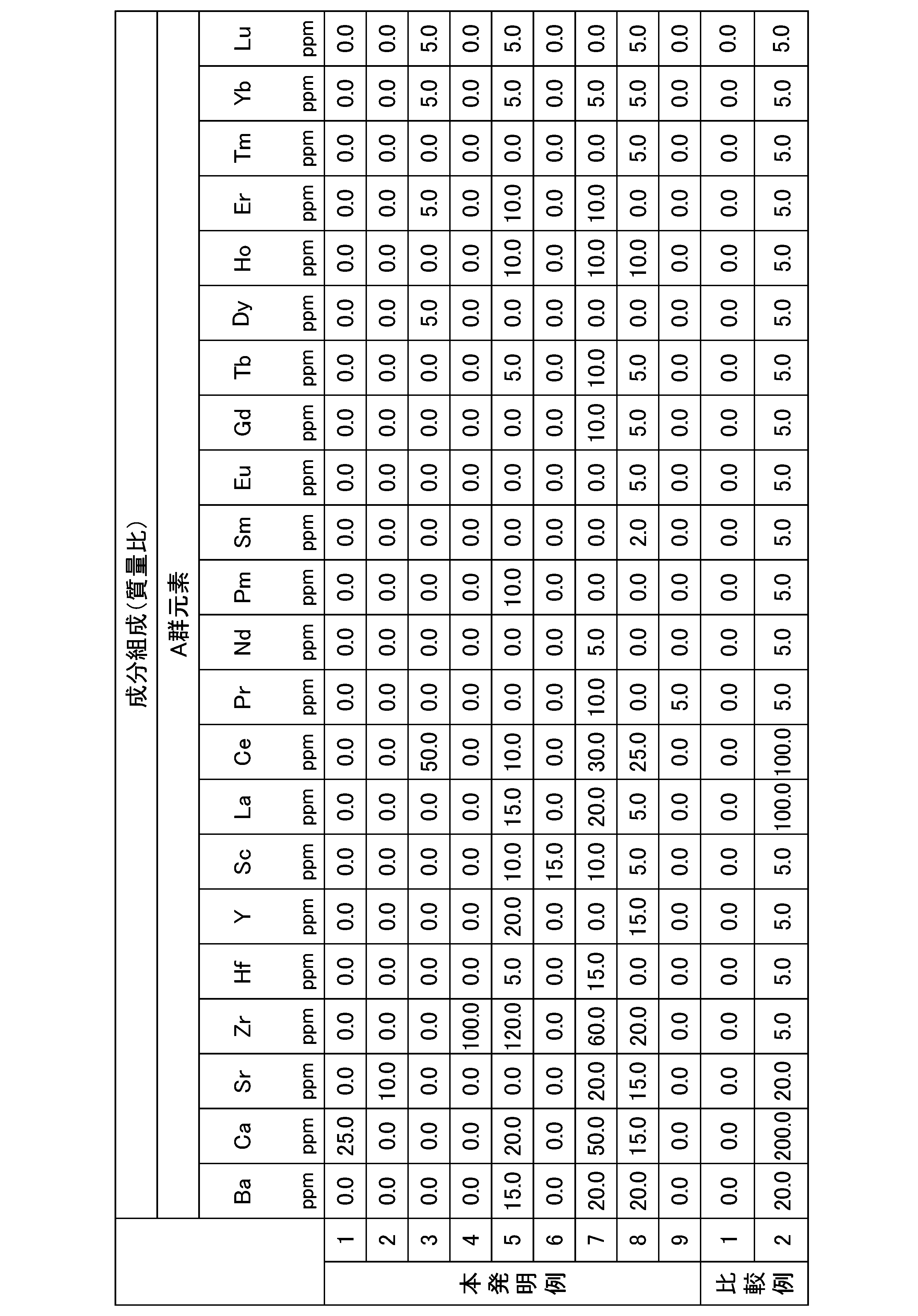
本発明例においては、冷熱サイクル実施後において、粒界三重点を中心に配置した測定視野におけるKAM値が0.25°以下の割合Cと、粒内におけるKAM値が0.25°以下の割合Dとの比C/Dが0.93以上1.05以下の範囲内であった。
また、本発明例においては、比較例(市販の無酸素銅)と同様に、セラミックス基板との接合界面から離間するにしたがい硬度が低下しており、セラミックス基板との接合界面から100μm離間した位置においては十分に低い値を示していることが確認される。
そして、本発明例においては、冷熱サイクル実施後においても接合率が高く、冷熱サイクル信頼性に優れていた。
また、本発明例においては、比較例(市販の無酸素銅)と同様に、セラミックス基板との接合界面から離間するにしたがい硬度が低下しており、セラミックス基板との接合界面から100μm離間した位置においては十分に低い値を示していることが確認される。
そして、本発明例においては、冷熱サイクル実施後においても接合率が高く、冷熱サイクル信頼性に優れていた。
本発明例によれば、厳しい冷熱サイクルを負荷した場合であっても、セラミックス基板(セラミックス部材)と銅板(銅部材)との接合性に優れ、冷熱サイクル信頼性に優れた絶縁回路基板(銅/セラミックス接合体)を提供可能であることが確認された。
本発明によれば、厳しい冷熱サイクルを負荷した場合であっても、セラミックス部材と銅部材との接合性に優れ、冷熱サイクル信頼性に優れた銅/セラミックス接合体を提供することが可能となる。
10 絶縁回路基板(銅/セラミックス接合体)
11 セラミックス基板(セラミックス部材)
12 回路層(銅部材)
13 金属層(銅部材)
18 化合物粒子
MP 測定点
11 セラミックス基板(セラミックス部材)
12 回路層(銅部材)
13 金属層(銅部材)
18 化合物粒子
MP 測定点
Claims (8)
- 銅部材と、セラミックス部材とが接合されてなる銅/セラミックス接合体であって、
前記銅部材は、Cuの含有量が99.96mass%以上とされており、
液槽にて-65℃で5分保持と150℃で5分保持を1サイクルとする熱サイクル試験を3000サイクル実施後において、前記銅部材の厚さ方向に沿った断面を観察し、
粒界三重点を中心に配置した測定視野におけるKAM値が0.25°以下の割合Cと、粒内におけるKAM値が0.25°の割合Dとの比C/Dが0.93以上1.05以下の範囲内であることを特徴とする銅/セラミックス接合体。 - 前記銅部材において、前記セラミックス部材との接合界面から100μm離間した位置におけるナノインデンテーション硬度が0.40GPa以上1.03GPa以下の範囲内であることを特徴とする請求項1に記載の銅/セラミックス接合体。
- 前記銅部材は、Ca,Ba,Sr,Zr,Hf,Y,Sc,La,Ce,Pr,Nd,Pm,Sm,Eu,Gd,Tb,Dy,Ho,Er,Tm,Yb,Luから選択される1種又は2種以上のA群元素、および、O,S,Se,Teから選択される1種又は2種以上のB群元素のいずれか一方又は両方を合計量で10massppm以上300massppm以下の範囲内で含有していることを特徴とする請求項1に記載の銅/セラミックス接合体。
- 前記銅部材に、Cuと、前記A群元素および前記B群元素のいずれか一方または両方と、を含む化合物粒子が析出していることを特徴とする請求項3に記載の銅/セラミックス接合体。
- セラミックス基板の表面に、銅板が接合されてなる絶縁回路基板であって、
前記銅板は、Cuの含有量が99.96mass%以上とされており、
液槽にて-65℃で5分保持と150℃で5分保持を1サイクルとする熱サイクル試験を3000サイクル実施後において、前記銅板の厚さ方向に沿った断面を観察し、
粒界三重点を中心に配置した測定視野におけるKAM値が0.25°以下の割合Cと、粒内におけるKAM値が0.25°以下の割合Dとの比C/Dが0.93以上1.05以下の範囲内であることを特徴とする絶縁回路基板。 - 前記銅板において、前記セラミックス基板との接合界面から100μm離間した位置におけるナノインデンテーション硬度が0.40GPa以上1.03GPa以下の範囲内であることを特徴とする請求項5に記載の絶縁回路基板。
- 前記銅板は、Ca,Ba,Sr,Zr,Hf,Y,Sc,La,Ce,Pr,Nd,Pm,Sm,Eu,Gd,Tb,Dy,Ho,Er,Tm,Yb,Luから選択される1種又は2種以上のA群元素、および、O,S,Se,Teから選択される1種又は2種以上のB群元素のいずれか一方又は両方を合計量で10massppm以上300massppm以下の範囲内で含有していることを特徴とする請求項5に記載の絶縁回路基板。
- 前記銅板に、Cuと、前記A群元素および前記B群元素のいずれか一方または両方と、を含む化合物粒子が析出していることを特徴とする請求項7に記載の絶縁回路基板。
Priority Applications (1)
| Application Number | Priority Date | Filing Date | Title |
|---|---|---|---|
| CN202480052151.3A CN121693482A (zh) | 2023-10-06 | 2024-10-01 | 铜-陶瓷接合体及绝缘电路基板 |
Applications Claiming Priority (4)
| Application Number | Priority Date | Filing Date | Title |
|---|---|---|---|
| JP2023-174525 | 2023-10-06 | ||
| JP2023174525 | 2023-10-06 | ||
| JP2024165171A JP2025065004A (ja) | 2023-10-06 | 2024-09-24 | 銅/セラミックス接合体、および、絶縁回路基板 |
| JP2024-165171 | 2024-09-24 |
Publications (1)
| Publication Number | Publication Date |
|---|---|
| WO2025074992A1 true WO2025074992A1 (ja) | 2025-04-10 |
Family
ID=95283350
Family Applications (1)
| Application Number | Title | Priority Date | Filing Date |
|---|---|---|---|
| PCT/JP2024/035090 Pending WO2025074992A1 (ja) | 2023-10-06 | 2024-10-01 | 銅/セラミックス接合体、および、絶縁回路基板 |
Country Status (2)
| Country | Link |
|---|---|
| CN (1) | CN121693482A (ja) |
| WO (1) | WO2025074992A1 (ja) |
Citations (5)
| Publication number | Priority date | Publication date | Assignee | Title |
|---|---|---|---|---|
| JPH0360185A (ja) * | 1989-07-28 | 1991-03-15 | Hitachi Cable Ltd | 銅配線セラミック基板の製造方法 |
| WO2013024813A1 (ja) * | 2011-08-12 | 2013-02-21 | 三菱マテリアル株式会社 | パワーモジュール用基板、ヒートシンク付パワーモジュール用基板、パワーモジュール及びパワーモジュール用基板の製造方法 |
| JP2016046356A (ja) * | 2014-08-21 | 2016-04-04 | 三菱マテリアル株式会社 | 放熱板付パワーモジュール用基板及びパワーモジュール |
| WO2020162445A1 (ja) * | 2019-02-04 | 2020-08-13 | 三菱マテリアル株式会社 | 銅/セラミックス接合体の製造方法、絶縁回路基板の製造方法、銅/セラミックス接合体、及び、絶縁回路基板 |
| WO2021200866A1 (ja) * | 2020-03-30 | 2021-10-07 | デンカ株式会社 | 回路基板、接合体、及びこれらの製造方法 |
-
2024
- 2024-10-01 WO PCT/JP2024/035090 patent/WO2025074992A1/ja active Pending
- 2024-10-01 CN CN202480052151.3A patent/CN121693482A/zh active Pending
Patent Citations (5)
| Publication number | Priority date | Publication date | Assignee | Title |
|---|---|---|---|---|
| JPH0360185A (ja) * | 1989-07-28 | 1991-03-15 | Hitachi Cable Ltd | 銅配線セラミック基板の製造方法 |
| WO2013024813A1 (ja) * | 2011-08-12 | 2013-02-21 | 三菱マテリアル株式会社 | パワーモジュール用基板、ヒートシンク付パワーモジュール用基板、パワーモジュール及びパワーモジュール用基板の製造方法 |
| JP2016046356A (ja) * | 2014-08-21 | 2016-04-04 | 三菱マテリアル株式会社 | 放熱板付パワーモジュール用基板及びパワーモジュール |
| WO2020162445A1 (ja) * | 2019-02-04 | 2020-08-13 | 三菱マテリアル株式会社 | 銅/セラミックス接合体の製造方法、絶縁回路基板の製造方法、銅/セラミックス接合体、及び、絶縁回路基板 |
| WO2021200866A1 (ja) * | 2020-03-30 | 2021-10-07 | デンカ株式会社 | 回路基板、接合体、及びこれらの製造方法 |
Also Published As
| Publication number | Publication date |
|---|---|
| CN121693482A (zh) | 2026-03-17 |
Similar Documents
| Publication | Publication Date | Title |
|---|---|---|
| CN109417056B (zh) | 铜-陶瓷接合体及绝缘电路基板 | |
| EP3590909B1 (en) | Copper/ceramic joined body insulated circuit board, method for producing copper/ceramic joined body, and method for producing insulated circuit board | |
| CN113348046B (zh) | 铜-陶瓷接合体的制造方法、绝缘电路基板的制造方法、铜-陶瓷接合体及绝缘电路基板 | |
| CN101861647B (zh) | 电源模块用基板的制造方法、电源模块用基板、和电源模块 | |
| US12027434B2 (en) | Bonded body of copper and ceramic, insulating circuit substrate, bonded body of copper and ceramic production method, and insulating circuit substrate production method | |
| CN114845977B (zh) | 铜-陶瓷接合体、及绝缘电路基板 | |
| WO2018003845A1 (ja) | 銅/セラミックス接合体、及び、絶縁回路基板 | |
| US10734297B2 (en) | Ag underlayer-attached metallic member, Ag underlayer-attached insulating circuit substrate,semiconductor device, heat sink-attached insulating circuit substrate, and method for manufacturing Ag underlayer-attached metallic member | |
| CN114728857A (zh) | 铜-陶瓷接合体、绝缘电路基板、铜-陶瓷接合体的制造方法及绝缘电路基板的制造方法 | |
| CN114342573B (zh) | 铜-陶瓷接合体及绝缘电路基板 | |
| JP6928297B2 (ja) | 銅/セラミックス接合体、及び、絶縁回路基板 | |
| WO2017150096A1 (ja) | 半導体装置 | |
| CN117769533A (zh) | 铜-陶瓷接合体及绝缘电路基板 | |
| JP2021098641A (ja) | 銅/セラミックス接合体、及び、絶縁回路基板 | |
| WO2025074992A1 (ja) | 銅/セラミックス接合体、および、絶縁回路基板 | |
| JP2025065004A (ja) | 銅/セラミックス接合体、および、絶縁回路基板 | |
| WO2025075015A1 (ja) | 銅/セラミックス接合体、および、絶縁回路基板 | |
| JP2025065002A (ja) | 銅/セラミックス接合体、および、絶縁回路基板 | |
| JP7694291B2 (ja) | 銅/セラミックス接合体、および、絶縁回路基板 | |
| WO2021117327A1 (ja) | 銅/セラミックス接合体、及び、絶縁回路基板 | |
| WO2021112046A1 (ja) | 銅/セラミックス接合体、絶縁回路基板、及び、銅/セラミックス接合体の製造方法、絶縁回路基板の製造方法 | |
| CN117897366B (zh) | 铜-陶瓷接合体及绝缘电路基板 | |
| JP7725907B2 (ja) | 銅/セラミックス接合体、および、絶縁回路基板 | |
| JP7540345B2 (ja) | 銅/セラミックス接合体、および、絶縁回路基板 | |
| JP6850984B2 (ja) | 銅/セラミックス接合体、絶縁回路基板、及び、銅/セラミックス接合体の製造方法、絶縁回路基板の製造方法 |
Legal Events
| Date | Code | Title | Description |
|---|---|---|---|
| 121 | Ep: the epo has been informed by wipo that ep was designated in this application |
Ref document number: 24874594 Country of ref document: EP Kind code of ref document: A1 |