WO2025062832A1 - 撮像装置、コンパレータおよび撮像方法 - Google Patents
撮像装置、コンパレータおよび撮像方法 Download PDFInfo
- Publication number
- WO2025062832A1 WO2025062832A1 PCT/JP2024/026937 JP2024026937W WO2025062832A1 WO 2025062832 A1 WO2025062832 A1 WO 2025062832A1 JP 2024026937 W JP2024026937 W JP 2024026937W WO 2025062832 A1 WO2025062832 A1 WO 2025062832A1
- Authority
- WO
- WIPO (PCT)
- Prior art keywords
- pixel
- switch
- transistor
- conversion
- phase
- Prior art date
- Legal status (The legal status is an assumption and is not a legal conclusion. Google has not performed a legal analysis and makes no representation as to the accuracy of the status listed.)
- Pending
Links
Images











Classifications
-
- H—ELECTRICITY
- H04—ELECTRIC COMMUNICATION TECHNIQUE
- H04N—PICTORIAL COMMUNICATION, e.g. TELEVISION
- H04N25/00—Circuitry of solid-state image sensors [SSIS]; Control thereof
- H04N25/70—SSIS architectures; Circuits associated therewith
- H04N25/76—Addressed sensors, e.g. MOS or CMOS sensors
-
- H—ELECTRICITY
- H04—ELECTRIC COMMUNICATION TECHNIQUE
- H04N—PICTORIAL COMMUNICATION, e.g. TELEVISION
- H04N25/00—Circuitry of solid-state image sensors [SSIS]; Control thereof
- H04N25/70—SSIS architectures; Circuits associated therewith
- H04N25/76—Addressed sensors, e.g. MOS or CMOS sensors
- H04N25/77—Pixel circuitry, e.g. memories, A/D converters, pixel amplifiers, shared circuits or shared components
- H04N25/771—Pixel circuitry, e.g. memories, A/D converters, pixel amplifiers, shared circuits or shared components comprising storage means other than floating diffusion
-
- H—ELECTRICITY
- H04—ELECTRIC COMMUNICATION TECHNIQUE
- H04N—PICTORIAL COMMUNICATION, e.g. TELEVISION
- H04N25/00—Circuitry of solid-state image sensors [SSIS]; Control thereof
- H04N25/70—SSIS architectures; Circuits associated therewith
- H04N25/76—Addressed sensors, e.g. MOS or CMOS sensors
- H04N25/78—Readout circuits for addressed sensors, e.g. output amplifiers or A/D converters
Definitions
- This technology relates to an imaging device, a comparator, and an imaging method. More specifically, this technology relates to an imaging device, a comparator, and an imaging method that can transfer photoelectrically converted electric charges and hold them in pixels.
- a capacitor that holds the charge transferred from the photoelectric conversion unit is provided in the pixel.
- an imaging device has been proposed that has a pixel including a capacitor that holds the charge transferred from the photoelectric conversion unit, and a floating diffusion to which the charge is transferred from the capacitor (see, for example, Patent Document 1).
- This technology was developed in light of these circumstances, and aims to make it possible to transfer charge from the capacitor to the floating diffusion while minimizing the drop in frame rate.
- This technology has been made to solve the problems mentioned above, and its first aspect is an imaging device that includes pixels capable of transferring and holding photoelectrically converted electric charges, and an AD conversion unit that can time-divisionally switch between AD (Analog to Digital) conversion of pixel signals read out from pixels in different rows in the same column.
- AD Analog to Digital
- the pixel may include a photoelectric conversion unit, a capacitor that holds charges photoelectrically converted by the photoelectric conversion unit, a first transfer transistor that transfers the charges photoelectrically converted by the photoelectric conversion unit to the capacitor, a second transfer transistor that transfers the charges held in the capacitor to a floating diffusion, an output transistor that outputs the pixel signal based on the charges transferred to the floating diffusion, and a selection transistor that selects the output of the pixel signal.
- the AD conversion unit may perform AD conversion of a pixel signal read from a second pixel in a second row in the first column during an AD conversion period that overlaps with a transfer period during which charge held in a capacitor of a first pixel in a first row in a first column is transferred to a floating diffusion. This brings about an effect that a pixel signal read from a second pixel in the same column as the first pixel is AD converted during charge transfer in the first pixel.
- a vertical signal line that transmits the pixel signal in the column direction, a first comparator whose input is connected to the vertical signal line, and a second comparator whose input is connected to the vertical signal line may be provided.
- pixel signals read from pixels in different rows in the same column are AD converted in a time-division manner.
- the first comparator may perform AD conversion of the P phase of the pixel signal read from the first pixel after the auto-zero operation of the first comparator
- the second comparator may perform AD conversion of the P phase of the pixel signal read from the first pixel after the auto-zero operation of the second comparator
- the second comparator may perform AD conversion of the P phase of the pixel signal read from the second pixel after the auto-zero operation of the second comparator
- the first comparator may perform AD conversion of the D phase of the pixel signal read from the first pixel after the AD conversion of the P phase of the pixel signal read from the second pixel
- the second comparator may perform AD conversion of the D phase of the pixel signal read from the second pixel after the AD conversion of the D phase of the pixel signal read from the first pixel.
- the AD conversion of the second comparator may be put on hold during the AD conversion of the first comparator, and the AD conversion of the first comparator may be put on hold during the AD conversion of the second comparator. This provides the effect of activating the comparator depending on the usage state of the comparator.
- a vertical signal line that transmits the pixel signal in the column direction, a comparator whose input is connected to the vertical signal line, a first switch connected between the input of the comparator and the vertical signal line, and a second switch connected between the input of the comparator and the vertical signal line may be provided.
- AD conversion of the pixel signal read out from the first pixel may be performed by the comparator
- AD conversion of the pixel signal read out from the second pixel may be performed by the comparator
- the pixel signal may include a vertical signal line that transmits the pixel signal in the column direction, and a comparator having a first input and a second input connected to the vertical signal line, the comparator including a first transistor, a second transistor, a third transistor capable of forming a differential pair with each of the first transistor and the second transistor, a fourth transistor capable of forming a differential pair with each of the first transistor and the second transistor, a first switch connected in series to the first transistor, a second switch connected in series to the second transistor, a third switch connected in series to the third transistor, and a fourth switch connected in series to the fourth transistor.
- a first capacitor connected in series to the gate of the first transistor, a second capacitor connected in series to the gate of the second transistor, a third capacitor connected in series to the gate of the third transistor, a fourth capacitor connected in series to the gate of the fourth transistor, a first auto-zero switch connected between the gate of the first transistor and the first switch, a second auto-zero switch connected between the gate of the second transistor and the second switch, a third auto-zero switch connected between the gate and drain of the third transistor, and a fourth auto-zero switch connected between the gate and drain of the fourth transistor may be provided. This provides the effect of realizing the auto-zero operation of the comparator while suppressing the influence of charge injection and feed-through caused by the switching operation of the input of a single comparator from being transmitted to the capacitor.
- the comparator when the first switch and the third switch are on and the second switch and the fourth switch are off, the first auto-zero switch and the third auto-zero switch are on to perform an auto-zero operation, and then the comparator performs AD conversion of the P phase of the pixel signal read out from the first pixel; when the first switch and the third switch are off and the second switch and the fourth switch are on, the second auto-zero switch and the fourth auto-zero switch are on to perform an auto-zero operation, and then the comparator performs AD conversion of the P phase of the pixel signal read out from the second pixel; when the first switch and the third switch are on and the second switch and the fourth switch are off, the comparator performs AD conversion of the D phase of the pixel signal read out from the first pixel; and when the first switch and the third switch are off and the second switch and the fourth switch are on, the comparator performs AD conversion of the D phase of the pixel signal read out from the second pixel. This results in pixel signals read from pixels in
- the pixel circuit may further include a first P-phase register that holds the P-phase AD conversion result of the pixel signal read from the first pixel, a second P-phase register that holds the P-phase AD conversion result of the pixel signal read from the second pixel, and a CDS processing unit that performs a first CDS (Correlated Double Sampling) process based on the P-phase AD conversion result of the pixel signal read from the first pixel held in the first P-phase register and the D-phase AD conversion result of the pixel signal read from the first pixel output from the AD conversion unit, and performs a second CDS process based on the P-phase AD conversion result of the pixel signal read from the second pixel held in the second P-phase register and the D-phase AD conversion result of the pixel signal read from the second pixel output from the AD conversion unit.
- This provides the effect of realizing CDS processing while AD converting pixel signals read from pixels in different rows in the same column in a time-division manner in a charge domain global shutter system
- the pixels may transfer and hold the photoelectrically converted charges based on a global shutter operation. This provides the effect of starting exposure simultaneously for all pixels.
- the second aspect is a comparator including a first transistor, a second transistor, a third transistor capable of forming a differential pair with each of the first transistor and the second transistor, a fourth transistor capable of forming a differential pair with each of the first transistor and the second transistor, a first switch connected in series to the first transistor, a second switch connected in series to the second transistor, a third switch connected in series to the third transistor, and a fourth switch connected in series to the fourth transistor.
- a first capacitor may be connected in series to the gate of the first transistor, a second capacitor may be connected in series to the gate of the second transistor, a third capacitor may be connected in series to the gate of the third transistor, a fourth capacitor may be connected in series to the gate of the fourth transistor, a first auto-zero switch may be connected between the gate of the first transistor and the first switch, a second auto-zero switch may be connected between the gate of the second transistor and the second switch, a third auto-zero switch may be connected between the gate and drain of the third transistor, and a fourth auto-zero switch may be connected between the gate and drain of the fourth transistor.
- the second switch and the fourth switch when the first switch and the third switch are turned on, the second switch and the fourth switch may be turned off, and when the first switch and the third switch are turned off, the second switch and the fourth switch may be turned on.
- the first auto-zero switch and the third auto-zero switch when the first switch and the third switch are on, the first auto-zero switch and the third auto-zero switch may be on, and when the second switch and the fourth switch are on, the second auto-zero switch and the fourth auto-zero switch may be on.
- the gate of the first transistor and the gate of the second transistor may be connected to the same signal line, and the gate of the third transistor and the gate of the fourth transistor may receive the same reference signal. This provides the effect of subjecting pixel signals read out from pixels in different rows in the same column to single-slope A/D conversion in a time-division manner.
- the third aspect is an imaging method in which a first pixel in a first row in a first column transfers and holds a photoelectrically converted charge in a capacitor in the first pixel, and a second pixel in a second row in the first column transfers and holds a photoelectrically converted charge in a capacitor in the second pixel, and an AD conversion unit performs AD conversion of a pixel signal read out from the second pixel during an AD conversion period that overlaps with a transfer period during which the charge held in the capacitor of the first pixel is transferred to a floating diffusion.
- 1 is a block diagram illustrating an example of a configuration of an imaging apparatus according to a first embodiment.
- 1 is a block diagram illustrating an example of a configuration of a solid-state imaging device according to a first embodiment.
- 2 is a diagram illustrating an example of a circuit configuration of a pixel of a solid-state imaging device according to the first embodiment;
- 2 is a block diagram showing a schematic configuration example of an AD conversion unit of a solid-state imaging device according to a first embodiment;
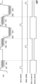
- 4 is a timing chart showing waveforms at various parts of a pixel during operation of the solid-state imaging device according to the first embodiment;
- 4 is a timing chart showing waveforms of vertical signal lines and each part of a pixel during AD conversion in the solid-state imaging device according to the first embodiment.
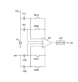
- FIG. 2 is a block diagram showing a configuration example of an AD conversion section for one column of a solid-state imaging device according to a first embodiment
- 5 is a timing chart showing an example of the operation of an AD conversion unit for one column of the solid-state imaging device according to the first embodiment
- 2 is a block diagram showing a configuration example of a column signal processing unit of a solid-state imaging device according to a first embodiment
- 4 is a timing chart showing an operation of a CDS process of the solid-state imaging device according to the first embodiment
- 13 is a block diagram showing an example of the configuration of an AD conversion unit for one column of a solid-state imaging device according to a second embodiment.
- FIG. 13 is a timing chart showing an example of the operation of an AD conversion unit for one column of a solid-state imaging device according to a second embodiment.
- FIG. 13 is a block diagram showing an example of the configuration of an AD conversion unit for one column of a solid-state imaging device according to a third embodiment.
- 13 is a timing chart showing an example of the operation of an AD conversion unit for one column of a solid-state imaging device according to a third embodiment.
- FIG. 13 is a block diagram showing an example of the configuration of an AD conversion unit for one column of a solid-state imaging device according to a fourth embodiment.
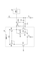
- FIG. 13 is a diagram illustrating an example of the configuration of a comparator for one column of a solid-state imaging device according to a fourth embodiment.
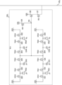
- FIG. 13 is a diagram illustrating an example of the configuration of a comparator for one column of a solid-state imaging device according to a fifth embodiment.
- FIG. 23 is a diagram illustrating an example of a circuit configuration of a pixel of a solid-state imaging device according to a sixth embodiment.
- FIG. 13 is a diagram showing a pixel readout order of a solid-state imaging device according to a sixth embodiment.
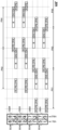
- 13 is a timing chart showing the operation of a solid-state imaging device according to a sixth embodiment.
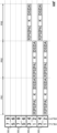
- 13 is a timing chart showing the operation of a solid-state imaging device according to the seventh embodiment.
- 23 is a timing chart showing the operation of a solid-state imaging device according to the eighth embodiment.
- FIG. 23 is a timing chart showing the operation of a solid-state imaging device according to a ninth embodiment.
- 23 is a timing chart showing the operation of the solid-state imaging device according to the tenth embodiment.
- FIG. 23 is a diagram showing the order in which pixels are read out from a solid-state imaging device according to an eleventh embodiment.
- 23 is a timing chart showing the operation of the solid-state imaging device according to the eleventh embodiment.
- 23 is a timing chart showing an example of the operation of an AD conversion unit for one column of a solid-state imaging device according to an eleventh embodiment.
- 23 is a timing chart showing the operation of a CDS process in a solid-state imaging device according to an eleventh embodiment;
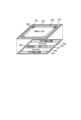
- FIG. 23 is a perspective view showing an example of a stack of a pixel array unit according to a twelfth embodiment
- 1 is a block diagram showing a schematic configuration example of a vehicle control system
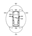
- FIG. 4 is an explanatory diagram showing an example of an installation position of an imaging unit.
- First embodiment an example in which pixel signals read from pixels in different rows in the same column are AD converted in a time-division manner based on the switching operation of two comparators.
- Second embodiment an example in which pixel signals read from pixels in different rows in the same column are AD converted in a time-division manner based on the switching operation of two comparators, and an unused comparator is put on standby.
- Third embodiment an example in which pixel signals read from pixels in different rows in the same column are AD converted in a time-division manner based on the input switching operation of a single comparator.
- Fourth embodiment an example in which pixel signals read from pixels in different rows in the same column are AD converted in a time-division manner based on the input switching operation of a single comparator, and a switch for switching the input is built into the comparator.
- Fifth embodiment an example in which pixel signals read out from pixels in different rows in the same column are AD converted in a time-division manner based on the switching operation of the input of a single comparator, a switch for switching the input is built into the comparator, and the auto-zero operation on the input side of the reference signal is omitted
- Sixth embodiment (example in which a charge domain is applied to each pixel of a four-pixel shared cell) 7.
- Seventh embodiment an example in which the reset period of a four-pixel shared cell to which a charge domain is applied is made different from the transfer period of the charge held in the capacitor.
- Eighth embodiment an example in which the reset period of a two-pixel shared cell to which a charge domain is applied is made different from the transfer period of the charge held in the capacitor.
- Ninth embodiment an example in which the reset period of a four-pixel shared cell to which a charge domain is applied is made different from the transfer period of the charge held in the capacitor and overlaps with the D-phase AD conversion period 10.
- Tenth embodiment an example in which the reset period of a two-pixel shared cell to which a charge domain is applied is made different from the transfer period of the charge held in the capacitor and overlaps with the D-phase AD conversion period
- Eleventh embodiment an example in which a process of putting AD conversion on hold during a transfer period of charge held in a capacitor in a charge domain and a process of executing AD conversion overlapping with a transfer period of charge held in a capacitor in a charge domain can be switched
- Twelfth embodiment example in which semiconductor chips forming a solid-state imaging device are stacked
- FIG. 1 is a block diagram showing an example of the configuration of an imaging apparatus according to the first embodiment.
- the imaging device 100 includes an optical system 101, a solid-state imaging device 102, an imaging control unit 103, an image processing unit 104, a storage unit 105, a display unit 106, and an operation unit 107.
- the imaging control unit 103, the image processing unit 104, the storage unit 105, the display unit 106, and the operation unit 107 are connected to each other via a bus 108.
- the imaging device 100 may be used as a standalone device, or may be incorporated into a mobile terminal such as a smartphone, an authentication device, a monitoring device, or may be incorporated into a vehicle or a drone.
- the optical system 101 allows light from a subject to be incident on the solid-state imaging device 102, and forms an optical image on the light receiving surface of the solid-state imaging device 102.
- the optical system 101 may include, for example, a focus lens, a zoom lens, and an aperture.
- the optical system 101 may also include multiple lenses, such as a wide-angle lens, a standard lens, and a telephoto lens.
- the solid-state imaging device 102 converts the optical image formed on the light receiving surface into an electrical signal for each pixel, digitizes the electrical signal, and outputs it. At this time, the solid-state imaging device 102 can operate based on a charge domain type global shutter method.
- the solid-state imaging device 102 is, for example, a CMOS (Complementary Metal Oxide Semiconductor) image sensor.
- the CMOS image sensor may be a back-illuminated image sensor or a front-illuminated image sensor.
- the light received by the solid-state imaging device 102 may be visible light, near infrared light (NIR: Near InfraRed), short wave infrared light (SWIR: Short Wavelength InfraRed), ultraviolet light, X-rays, or the like.
- NIR Near InfraRed
- SWIR Short Wavelength InfraRed
- ultraviolet light X-rays, or the like.
- the imaging control unit 103 controls imaging by the solid-state imaging device 102 based on commands from the operation unit 107. At this time, the imaging control unit 103 can control the exposure time, exposure amount, imaging timing, etc. of the solid-state imaging device 102.
- the image processing unit 104 performs image processing based on the output from the solid-state imaging device 102.
- the image processing includes, for example, gamma correction, white balance processing, sharpness processing, and tone conversion processing.
- the image processing unit 104 may include a processor that executes processing based on software.
- the storage unit 105 stores images captured by the solid-state imaging device 102, and stores imaging parameters of the solid-state imaging device 102.
- the storage unit 105 can also store programs that operate the imaging device 100 based on software.
- the storage unit 105 may include a ROM (Read Only Memory), a RAM (Random Access Memory), and a memory card.
- the display unit 106 displays captured images and various information that supports the imaging operation.
- the display unit 106 may be a liquid crystal display or an organic EL (Electro Luminescence) display.
- the operation unit 107 provides a user interface for operating the imaging device 100.
- the operation unit 107 may include, for example, buttons, dials, and switches provided on the imaging device 100.
- the operation unit 107 may be configured as a touch panel together with the display unit 106.
- the imaging device 100 may have additional functions that are not disclosed.
- FIG. 2 is a block diagram showing an example of the configuration of a solid-state imaging device according to the first embodiment.
- the solid-state imaging device 102 includes a pixel array section 111, a vertical scanning circuit 112, a column readout circuit 113, a column signal processing section 114, a horizontal scanning circuit 115, and a control circuit 116.
- the pixel array section 111 includes a plurality of pixels PIX.
- the pixels PIX are arranged in a matrix along the row direction (also called the horizontal direction) and the column direction (also called the vertical direction).
- Each pixel PIX can transfer and hold photoelectrically converted charges based on a global shutter operation.
- Each pixel PIX can form a source follower for each column between itself and the column readout circuit 113 when reading out a signal.
- Each pixel PIX is connected to a horizontal drive line HSL for each row, and to a vertical signal line VSL for each column.
- the horizontal drive line HSL drives each pixel PIX for each row when reading out a signal from each pixel PIX.
- the vertical signal line VSL transmits a potential based on a current flowing when reading out a signal from the pixel PIX to the column signal processing section 114 for each column.
- the vertical scanning circuit 112 scans the pixels PIX to be read in the column direction.
- the vertical scanning circuit 112 may be configured using a vertical register.
- the column readout circuit 113 can form a source follower for each column between each pixel PIX and the pixel PIX via the vertical signal line VSL. At this time, the column readout circuit 113 can change the potential of the vertical signal line VSL based on the charge held in the pixel PIX.
- the column signal processing unit 114 processes signals transmitted in the column direction from each pixel PIX.
- the column signal processing unit 114 can perform correlated double sampling (CDS) processing based on the signals transmitted in the column direction from each pixel PIX.
- CDS correlated double sampling
- the column signal processing unit 114 can also perform AD (Analog to Digital) conversion processing based on the signals transmitted in the column direction from each pixel PIX, and output the image signal Gout.
- AD Analog to Digital
- the column signal processing unit 114 includes a column ADC unit 114A.
- the column ADC unit 114A can perform AD conversion processing in parallel for each column.
- the column ADC unit 114A can perform AD conversion for each column based on the result of comparing the pixel signal read from the pixel PIX with a reference signal.
- the column ADC unit 114A can time-divisionally switch between AD conversion of pixel signals read from pixels in different rows in the same column.
- the column ADC unit 114A is an example of an AD conversion unit as described in the claims.
- the horizontal scanning circuit 115 scans the pixels PIX to be read in the row direction.
- the horizontal scanning circuit 115 may be configured using a horizontal register.
- the control circuit 116 controls the vertical scanning circuit 112, the column readout circuit 113, the column signal processing unit 114, and the horizontal scanning circuit 115.
- the control circuit 116 can control the scanning timing in the column direction, the scanning timing in the row direction, the operation timing of the column readout circuit 113, and the processing timing of the column signal processing unit 114.
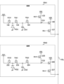
- FIG. 3 is a diagram showing an example of the circuit configuration of a pixel of a solid-state imaging device according to the first embodiment. Note that the diagram shows the configuration of two pixels in the same column but different rows.
- each pixel PIX1, PIX2 includes a photodiode PD1, PD2, a floating diffusion FD1, FD2, a capacitor CA1, CA2, and an overflow control transistor 122, 222. Furthermore, each pixel PIX1, PIX2 includes a transfer transistor 123, 124, 223, 224, a reset transistor 125, 225, an output transistor 126, 226, and a selection transistor 127, 227.
- Overflow control transistors 122, 222, transfer transistors 123, 124, 223, 224, reset transistors 125, 225, output transistors 126, 226 and selection transistors 127, 227 may be MOS (Metal Oxide Semiconductor) transistors.
- Capacitors CA1, CA2 may be MIM (Metal Insulation Metal) capacitance or junction capacitance formed on a semiconductor substrate.
- Each photodiode PD1, PD2 performs photoelectric conversion and accumulates the photoelectrically converted charge.
- Each photodiode PD1, PD2 is an example of a photoelectric conversion unit described in the claims.
- Each capacitor CA1, CA2 holds the charge transferred from each photodiode PD1, PD2. The transfer of charge from each photodiode PD1, PD2 to each capacitor CA1, CA2 may be performed simultaneously for all pixels.
- Each overflow control transistor 122, 222 controls the overflow of charge from each photodiode PD1, PD2.
- Each transfer transistor 123, 223 transfers the charge stored in each photodiode PD1, PD2 to each capacitor CA1, CA2.
- Each transfer transistor 124, 224 transfers the charge held in each capacitor CA1, CA2 to each floating diffusion FD1, FD2.
- Each reset transistor 125, 225 resets each floating diffusion FD1, FD2.
- Each output transistor 126, 226 outputs a signal according to the potential of each floating diffusion FD1, FD2.
- Each selection transistor 127, 227 selects the output of each output transistor 126, 226.
- the output transistor 126 and the selection transistor 127 are connected in series.
- the cathode of the photodiode PD1 is connected to the overflow potential OFD via the overflow control transistor 122.
- the cathode of the photodiode PD1 is connected to the capacitor CA1 via the transfer transistor 123.
- the capacitor CA1 is connected to the floating diffusion FD1 via the transfer transistor 124.
- the floating diffusion FD1 is connected to the reset voltage VRS via the reset transistor 125.
- the series circuit of the output transistor 126 and the selection transistor 127 is connected between the power supply voltage VDD and the vertical signal line VSL.
- the gate of the output transistor 126 is connected to the floating diffusion FD1.
- the output transistor 226 and the selection transistor 227 are connected in series.
- the cathode of the photodiode PD2 is connected to the overflow potential OFD via the overflow control transistor 222.
- the cathode of the photodiode PD2 is connected to the capacitor CA2 via the transfer transistor 223.
- the capacitor CA2 is connected to the floating diffusion FD2 via the transfer transistor 224.
- the floating diffusion FD2 is connected to the reset voltage VRS via the reset transistor 225.
- the series circuit of the output transistor 226 and the selection transistor 227 is connected between the power supply voltage VDD and the vertical signal line VSL.
- the gate of the output transistor 226 is connected to the floating diffusion FD2.
- Overflow control signals OFG1, OFG2 are applied to the gates of the overflow control transistors 122, 222. Transfer signals TRX1, TRX2 are applied to the gates of the transfer transistors 123, 223. Transfer signals TRG1, TRG2 are applied to the gates of the transfer transistors 124, 224. Reset signals RST1, RST2 are applied to the gates of the reset transistors 125, 225. Selection signals SEL1, SEL2 are applied to the gates of the selection transistors 127, 227.
- the overflow control signals OFG1, OFG2, transfer signals TRX1, TRX2, TRG1, TRG2, reset signals RST1, RST2, and selection signals SEL1, SEL2 can be transmitted to the pixels PIX1, PIX2 via the horizontal drive line HSL in FIG. 2.
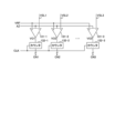
- FIG. 4 is a block diagram showing an example of the schematic configuration of an AD conversion unit of a solid-state imaging device according to the first embodiment.
- the column ADC unit 114A in FIG. 2 includes comparison units 131-1 to 131-3 and counters 132-1 to 132-3 for each column.
- Vertical signal lines VSL1 to VSL3 are provided for each column.
- Each comparison unit 131-1 to 131-3 compares the pixel signal transmitted via each vertical signal line VSL1 to VSL3 with a reference signal VRF, and outputs each comparison result VO1 to VO3 to the counters 132-1 to 132-3.
- the reference signal VRF may include a ramp signal.
- each comparison unit 131-1 to 131-3 can time-divisionally switch the AD conversion of pixel signals read out from pixels in different rows in the same column.
- each comparison unit 131-1 to 131-3 may include a single or multiple comparators for each column that time-divisionally switch and input pixel signals read out from pixels in different rows in the same column.
- an auto-zero signal AZ is input to each of the comparison units 131-1 to 131-3.
- the auto-zero signal AZ activates the auto-zero operation during the auto-zero period.
- a charge that balances the non-inverting input and the inverting input of each of the comparison units 131-1 to 131-3 can be stored in a DC blocking capacitor.
- a clock signal CKL is input to each of the counters 132-1 to 132-3.
- each of the counters 132-1 to 132-3 performs a counting operation based on the output timing of each of the comparison results VO1 to VO3 output from each of the comparison units 131-1 to 131-3.
- each of the counters 132-1 to 132-3 digitizes the pixel signals transmitted via each of the vertical signal lines VSL1 to VSL3 based on the count values CN1 to CN3 based on the counting operation.
- FIG. 5 is a timing chart showing waveforms at various parts of a pixel during operation of a solid-state imaging device according to the first embodiment.
- the operation of pixel PIX1 in FIG. 3 is taken as an example.
- a shows the waveform when charge is transmitted from photodiode PD1 to capacitor CA1.
- b shows the waveform when pixel PIX1 is shuttered.
- c shows the waveform when a pixel signal is read out from pixel PIX1.
- selection signal SEL1 when charge is being transferred from photodiode PD1 to capacitor CA1, selection signal SEL1 is set to a low level and selection transistor 127 is turned off. Then, transfer signal TRG1 and reset signal RST1 rise (t1), and transfer transistor 124 and reset transistor 125 are turned on, resetting capacitor CA1 and floating diffusion FD1.
- the transfer signal TRG1 and the reset signal RST1 fall in sequence, and then the transfer signal TRX1 rises (t2).
- the transfer transistor 123 turns on while the transfer transistor 124 and the reset transistor 125 are off, and the charge stored in the photodiode PD1 is transferred to the capacitor CA1.
- the overflow control signal OFG1 rises (t3).
- the transfer signals TRX1, TRG1, reset signal RST1, and selection signal SEL1 are set to a low level. Then, the overflow control signal OFG1 falls (t4), and the overflow control transistor 122 turns off. This shuttering operation can be performed simultaneously for all pixels, including pixel PIX1, and exposure can start simultaneously for all pixels.
- the overflow control signal OFG1 when reading out the pixel signal, the overflow control signal OFG1 is set to a high level, the transfer signal TRX1 is set to a low level, the overflow control transistor 122 is turned on, and the selection transistor 127 is turned off. Then, the reset signal RST1 and the selection signal SEL1 rise (t5), and the reset transistor 125 and the selection transistor 127 are turned on. At this time, the floating diffusion FD1 is reset, and the P-phase level of the floating diffusion FD1 is transmitted via the vertical signal line VSL.
- the reset signal RST1 falls, and while the reset transistor 125 is turned off, the transfer signal TRG1 rises and the transfer transistor 124 is turned on (t6). At this time, the charge held in the capacitor CA1 is transferred to the floating diffusion FD1, and the D-phase level of the floating diffusion FD1 is transmitted via the vertical signal line VSL.
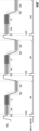
- FIG. 6 is a timing chart showing the waveforms of the vertical signal lines and each part of the pixels during AD conversion in the solid-state imaging device according to the first embodiment. Note that this figure shows the waveforms of each part of the pixels PIX1 and PIX2 in FIG. 3 and the waveform of the vertical signal line VSL during AD conversion.
- the P-phase settling period PS2 and P-phase AD conversion period PA2 of pixel PIX2 are set so as to overlap with the charge transfer period K1 from capacitor CA1 of pixel PIX1 to floating diffusion FD1. Also, the P-phase settling period PS1 and P-phase AD conversion period PA1 of pixel PIX1 are set so as to overlap with the charge transfer period K2 from capacitor CA2 of pixel PIX2 to floating diffusion FD2.
- the transfer signals TRX1 and TRX2 are always set to a low level. Then, after the selection signal SEL1 rises, the reset signal RST1 rises (t11), and the potential of the vertical signal line VSL is set according to the P-phase level of the floating diffusion FD1. Then, the reset signal RST1 falls, and after P-phase settling of the pixel PIX1 is performed (PS1), P-phase AD conversion is performed (PA1).
- selection signal SEL1 falls and selection signal SEL2 rises (t12).
- the reset signal RST2 rises (t13), and the potential of the vertical signal line VSL is set according to the P-phase level of the floating diffusion FD2. Then, the reset signal RST2 falls, and after P-phase settling of the pixel PIX2 is performed (PS2), P-phase AD conversion is performed (PA2).
- the transfer signal TRG1 rises at the falling edge of the reset signal RST2, and after the charge stored in the photodiode PD1 is transferred to the capacitor CA1, the transfer signal TRG1 falls.
- the selection signal SEL1 rises and the selection signal SEL2 falls (t14), and the potential of the vertical signal line VSL is set according to the D-phase level of the floating diffusion FD1. Then, after D-phase settling of the pixel PIX1 is performed (DS1), D-phase AD conversion is performed (DA1).
- the reset signal RST1 rises (t15), and the potential of the vertical signal line VSL is set according to the P-phase level of the floating diffusion FD1. Then, the reset signal RST1 falls, and after P-phase settling of the pixel PIX1 is performed (PS1), P-phase AD conversion is performed (PA1).
- the transfer signal TRG2 rises at the falling edge of the reset signal RST1, and after the charge stored in the photodiode PD2 is transferred to the capacitor CA2, the transfer signal TRG2 falls.
- the selection signal SEL1 falls and the selection signal SEL2 rises (t16), and the potential of the vertical signal line VSL is set according to the D-phase level of the floating diffusion FD2. Then, after D-phase settling of the pixel PIX2 is performed (DS2), D-phase AD conversion is performed (DA2).
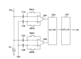
- FIG. 7 is a block diagram showing an example of the configuration of an AD conversion section for one column of a solid-state imaging device according to the first embodiment.
- the column ADC unit 114A includes comparators CM1 and CM2, a selector SEC, and a counter CNT.
- the inverting input terminals of the comparators CM1 and CM2 are connected to the vertical signal line VSL via capacitors C1A and C2A, respectively.
- the reference signal VRF is input to the non-inverting input terminals of the comparators CM1 and CM2 via capacitors C1B and C2B, respectively.
- An auto-zero switch SW1A is connected between the gate and drain of the differential transistor on the inverting input side of the comparator CM1.
- An auto-zero switch SW1B is connected between the gate and drain of the differential transistor on the non-inverting input side of the comparator CM1.
- An auto-zero switch SW2A is connected between the gate and drain of the differential transistor on the inverting input side of the comparator CM2.
- An auto-zero switch SW2B is connected between the gate and drain of the differential transistor on the non-inverting input side of the comparator CM2.
- the outputs of the comparators CM1 and CM2 are input to the counter CNT.
- the vertical signal line VSL is grounded via the current source 151.
- the selector SEC switches the output of each comparator CM1, CM2 and inputs it to the counter CNT.
- the counter CNT performs a counting operation based on the output timing of each comparison result output from each comparator CM1, CM2. At this time, the counter CNT digitizes the pixel signal transmitted via the vertical signal line VSL based on the count value CN based on the counting operation.
- FIG. 8 is a timing chart showing an example of the operation of the AD conversion unit for one column of the solid-state imaging device according to the first embodiment.
- the selector SEC switches the output of each comparator CM1, CM2 according to the read timing of each pixel PIX1, PIX2.
- the auto-zero period AZ1 of the comparator CM1 is set by turning on the auto-zero switches SW1A, SW1B while the comparator CM1 is selected.
- the P-phase settling period PS1 is set during the auto-zero period AZ1.
- the auto-zero switches SW2A, SW2B are turned on while the comparator CM2 is selected, and the auto-zero period AZ2 of the comparator CM2 is set.
- the P-phase settling period PS2 is set during the auto-zero period AZ2.
- FIG. 9 is a block diagram showing an example of the configuration of a column signal processing unit of a solid-state imaging device according to the first embodiment.
- the column signal processing unit 114 in FIG. 2 includes a counter unit CNB, P-phase registers 161 and 162, a CDS processing unit 163, and an output register 164.
- the counter unit CNB includes a counter CNT as shown in FIG. 7 for each column.
- the comparison results VO of the comparators CM1 and CM2 are input to the counter unit CNB for each column.
- P-phase register 161 stores the P-phase AD conversion result PN1 of pixel PIX1.
- P-phase register 162 stores the P-phase AD conversion result PN2 of pixel PIX2.
- Each of the P-phase registers 161 and 162 may be a line memory.
- the CDS processing unit 163 reads out the P-phase AD conversion result PN1 of pixel PIX1 from the P-phase register 161 based on the output timing of the D-phase AD conversion result DN1 of pixel PIX1 from the counter unit CNB. The CDS processing unit 163 then performs CDS processing based on the P-phase AD conversion result PN1 and the D-phase AD conversion result DN1. The CDS processing unit 163 also reads out the P-phase AD conversion result PN2 of pixel PIX2 from the P-phase register 162 based on the output timing of the D-phase AD conversion result DN2 of pixel PIX2 from the counter unit CNB. The CDS processing unit 163 then performs CDS processing based on the P-phase AD conversion result PN2 and the D-phase AD conversion result DN2.
- the output register 164 stores the CDS processing results CS1 and CS2 of each pixel PIX1 and PIX2 calculated by the CDS processing unit 163, and outputs them at a predetermined timing.
- FIG. 10 is a timing chart showing the operation of the CDS process of the solid-state imaging device according to the first embodiment.
- a P-phase count period CT1 is provided during a P-phase AD conversion period PA1 of pixel PIX1.
- a P-phase count period CT2 is provided during a P-phase AD conversion period PA2 of pixel PIX2.
- a D-phase count period CT3 is provided during a D-phase AD conversion period DA1 of pixel PIX1.
- a D-phase count period CT4 is provided during a D-phase AD conversion period DA2 of pixel PIX2.
- the P-phase AD conversion result PN1 is stored in the P-phase register 161 (ST1).
- the P-phase AD conversion result PN2 is stored in the P-phase register 162 (ST2).
- pixel signals read from pixels in different rows in the same column are AD converted in a time-division manner based on the switching operation of the two comparators CM1 and CM2.
- This makes it possible to AD convert the pixel signals read from each of the pixels PIX1 and PIX2 in the same column without providing a waiting period before AD conversion for each of the pixels PIX1 and PIX2. Therefore, in the charge domain type global shutter method, it is possible to improve the frame rate without changing the configuration of each of the pixels PIX1 and PIX2.
- Second embodiment In the first embodiment described above, pixel signals read from pixels in different rows in the same column are AD converted in a time-division manner based on the switching operation of the two comparators CM1 and CM2. In this second embodiment, pixel signals read from pixels in different rows in the same column are AD converted in a time-division manner based on the switching operation of the two comparators, and an unused comparator is put on standby.
- FIG. 11 is a block diagram showing an example of the configuration of an AD conversion section for one column of a solid-state imaging device according to the second embodiment.
- this solid-state imaging device has comparators CM1' and CM2' instead of the comparators CM1 and CM2 of the first embodiment described above.
- the rest of the configuration of the solid-state imaging device of the second embodiment is the same as the configuration of the solid-state imaging device of the first embodiment described above.
- Each of the comparators CM1', CM2' receives an enable signal EN1, EN2.
- Each of the comparators CM1', CM2' is activated based on the enable signal EN1, EN2.
- the rest of the configuration of the comparators CM1', CM2' in the second embodiment is the same as the configuration of the comparators CM1, CM2 in the first embodiment described above.
- FIG. 12 is a timing chart showing an example of the operation of an AD conversion unit for one column of a solid-state imaging device according to the second embodiment.
- enable signal EN1 is set to high level and enable signal EN2 is set to low level.
- enable signal EN1 is at high level
- comparator CM1' is selected by selector SEC.
- comparator CM1' is activated, enabling AD conversion, and comparator CM2' is deactivated, transitioning to waiting period WA2.
- the enable signal EN1 is set to low level and the enable signal EN2 is set to high level.
- the comparator CM2' is selected by the selector SEC. At this time, the comparator CM1' is deactivated and the process moves to the waiting period WA1, while the comparator CM2' is activated, enabling AD conversion.
- pixel signals read from pixels in different rows in the same column are AD converted in a time-division manner based on the switching operation of the two comparators CM1', CM2', and the unused comparators CM1', CM2' are put on standby.
- pixel signals read from pixels in different rows in the same column are AD converted in a time-division manner based on the switching operation of two comparators CM1 and CM2.
- pixel signals read from pixels in different rows in the same column are AD converted in a time-division manner based on the switching operation of the input of a single comparator.
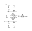
- this solid-state imaging device includes a comparator CM and switches SW11A, SW11B, SW12A, and SW12B instead of the comparators CM1 and CM2 of the first embodiment described above.
- the rest of the configuration of the solid-state imaging device of the third embodiment is the same as that of the solid-state imaging device of the first embodiment described above.
- the switches SW11A and SW12A can switch the input of the pixel signals of the pixels PIX1 and PIX2 transmitted through the same vertical signal line VSL to the comparator CM.
- the switches SW11B and SW12B can switch the capacitors C1B and C2B used to input the reference signal VRF in conjunction with switching the input of the pixel signals of the pixels PIX1 and PIX2 to the comparator CM.
- the switch SW11A is connected between the inverting input terminal of the comparator CM and the capacitor C1A.
- the switch SW12A is connected between the inverting input terminal of the comparator CM and the capacitor C2A.
- the switch SW11B is connected between the non-inverting input terminal of the comparator CM and the capacitor C1B.
- the switch SW12B is connected between the non-inverting input terminal of the comparator CM and the capacitor C2B.
- the output of the comparator CM is input to the counter CNT.
- FIG. 14 is a timing chart showing an example of the operation of an AD conversion unit for one column of a solid-state imaging device according to the third embodiment.
- the switches SW11A and SW11B are turned off and the switches SW12A and SW12B are turned on.
- the pixel signal of pixel PIX2 is input to the comparator CM.
- charge is accumulated in the capacitors C2A and C2B so that the inverting input and non-inverting input of the comparator CM are balanced.
- pixel signals read from pixels in different rows in the same column are AD converted in a time-division manner based on the input switching operation of a single comparator CM. This makes it possible to suppress an increase in the circuit scale of the AD conversion unit while eliminating the need for a waiting period before AD conversion for each of the pixels PIX1 and PIX2 in the same column.
- pixel signals read from pixels in different rows in the same column are AD converted in a time-division manner based on the input switching operation of a single comparator CM.
- pixel signals read from pixels in different rows in the same column are AD converted in a time-division manner based on the input switching operation of a single comparator, and a switch for switching the input is built into the comparator.
- FIG. 15 is a block diagram showing an example of the configuration of an AD conversion unit for one column of a solid-state imaging device according to the fourth embodiment.
- this solid-state imaging device has a comparator CM' instead of the comparator CM of the third embodiment described above.
- the switches SW11A, SW11B, SW12A, and SW12B of the third embodiment described above are built into the comparator CM'.
- the comparator CM' is provided with inverting input terminals corresponding to the switches SW11A and SW11B, and with non-inverting input terminals corresponding to the switches SW12A and SW12B.
- the rest of the configuration of the solid-state imaging device of the fourth embodiment is the same as that of the solid-state imaging device of the third embodiment described above.
- the comparator CM' can operate at the same timing as the comparator CM of the third embodiment described above.
- FIG. 16 is a diagram showing an example of the configuration of a comparator for one column of a solid-state imaging device according to the fourth embodiment.
- the comparator CM' includes a differential amplifier 201 and a rear-stage amplifier 202.
- the rear-stage amplifier 202 is connected to the rear stage of the differential amplifier 201.
- the rear-stage amplifier 202 may be a multi-stage amplifier.
- the differential amplifier 201 includes P-channel field effect transistors M0A and M0B, N-channel field effect transistors M1A, M1B, M2A, and M2B, switches SW11A, SW11B, SW12A, and SW12B, and a current source 211.
- the P-channel field effect transistor M0A can form a differential pair with each of the N-channel field effect transistors M1A and M2A.
- the P-channel field effect transistor M0B can form a differential pair with each of the N-channel field effect transistors M1B and M2B.
- the P-channel field effect transistors M0A and M0B can form a current mirror.
- each P-channel field effect transistor M0A, M0B is connected to the power supply potential VDD.
- the gate of each P-channel field effect transistor M0A, M0B is connected to the drain of the P-channel field effect transistor M0B.
- a switch SW11A is connected between the drain of the P-channel field effect transistor M0A and the drain of the N-channel field effect transistor M1A.
- a switch SW12A is connected between the drain of the P-channel field effect transistor M0A and the drain of the N-channel field effect transistor M2A.
- a switch SW11B is connected between the drain of the P-channel field effect transistor M0B and the drain of the N-channel field effect transistor M1B.
- a switch SW12B is connected between the drain of the P-channel field effect transistor M0B and the drain of the N-channel field effect transistor M2B.
- the sources of the N-channel field effect transistors M1A, M2A, M1B, and M2B are grounded via a current source 211.
- An auto-zero switch SW1A is connected between the drain of the P-channel field effect transistor M0A and the gate of the N-channel field effect transistor M1A.
- An auto-zero switch SW2A is connected between the drain of the P-channel field effect transistor M0A and the gate of the N-channel field effect transistor M2A.
- An auto-zero switch SW1B is connected between the drain of the P-channel field effect transistor M0B and the gate of the N-channel field effect transistor M1B.
- An auto-zero switch SW2B is connected between the drain of the P-channel field effect transistor M0B and the gate of the N-channel field effect transistor M2B.
- a capacitor C1A is connected between the vertical signal line VSL and the gate of the N-channel field effect transistor M1A.
- a capacitor C2A is connected between the vertical signal line VSL and the gate of the N-channel field effect transistor M2A.
- a reference signal VRF is input to the gate of the N-channel field effect transistor M1B via the capacitor C1B.
- a reference signal VRF is input to the gate of the N-channel field effect transistor M2B via the capacitor C2B.
- the comparator CM' may also be used for AD conversion of analog signals such as audio signals, temperature, pressure, flow speed, wind speed, and vehicle speed. Alternatively, the comparator CM' may be used to compare signals other than those used for AD conversion with a threshold value.
- FIG. 17 is a diagram showing an example of the configuration of a comparator for one column of a solid-state imaging device according to the fifth embodiment.
- this solid-state imaging device has a differential amplifier 301 instead of the differential amplifier 201 of the above-mentioned fourth embodiment.
- this solid-state imaging device does not have the auto-zero switches SW1B and SW2B and the capacitors C1B and C2B of the above-mentioned fourth embodiment.
- the rest of the configuration of the solid-state imaging device of the fifth embodiment is the same as the configuration of the solid-state imaging device of the above-mentioned fourth embodiment.
- Differential amplifier 301 is obtained by removing N-channel field effect transistor M2B and switches SW11B and SW12B from differential amplifier 201 of the above-mentioned fourth embodiment. At this time, the drain of N-channel field effect transistor M1B is connected to the drain of P-channel field effect transistor M0B. The rest of the configuration of differential amplifier 301 of the fifth embodiment is the same as the configuration of differential amplifier 201 of the above-mentioned fourth embodiment.
- the switching of the auto-zero switches SW1A, SW2A and the switches SW11A, SW12A is the same as that of the differential amplifier 201 in the fourth embodiment described above.
- the auto-zero operation is performed on the input side of the pixel signal via the vertical signal line VSL, and the auto-zero operation is omitted on the input side of the reference signal VRF.
- the auto-zero potential depends on the potential of the reference signal VRF, and that the absolute value precision of the potential of the reference signal VRF is ensured.
- the switches SW11A and SW11B for switching the input are built into the comparator, and the auto-zero operation on the input side of the reference signal VRF is omitted.
- This makes it possible to eliminate the need for auto-zero switches SW1B and SW2B, switches SW11B and SW12B, and capacitors C1B and C2B on the input side of the reference signal VRF.
- This makes it possible to suppress the effects of charge injection and feed-through caused by the input switching operation of a single comparator while suppressing an increase in the circuit scale of the AD conversion unit.
- FIG. 18 is a diagram showing an example of the circuit configuration of a pixel of a solid-state imaging device according to the sixth embodiment.
- this solid-state imaging device has a four-pixel shared cell CEL instead of the pixel PIX of the first embodiment described above.
- the rest of the configuration of the solid-state imaging device of the sixth embodiment is the same as the configuration of the solid-state imaging device of the first embodiment described above.
- the four-pixel shared cell CEL adds photodiodes PD2 to PD4, capacitors CA2 to CA4, transfer transistors 223, 224, 323, 324, 423, 424, and overflow control transistors 222 to 422 to pixel PIX1 of the first embodiment described above.
- the connection relationships of the photodiodes PD2 to PD4, the capacitors CA2 to CA4, the transfer transistors 223, 224, 323, 324, 423, 424, and the overflow control transistors 222 to 422 are the same as the connection relationships of the photodiode PD1, capacitor CA1, transfer transistors 123, 124, and overflow control transistor 122.
- the floating diffusion FD1, reset transistor 125, output transistor 126, and selection transistor 127 are shared by the four photodiodes PD1 to PD4 and the four capacitors CA1 to CA4.
- a reset signal RST is applied to the gate of the reset transistor 125
- a selection signal SEL is applied to the gate of the selection transistor 127.
- pixels can be arranged in a 2x2 array. In this case, the four-pixel shared cell CEL can perform colorization based on the Bayer arrangement.
- FIG. 19 shows the pixel readout order of a solid-state imaging device according to the sixth embodiment.
- the four-pixel shared cells CEL are arranged in a matrix along the row and column directions.
- each vertical signal line VSL1 to VSLn (n is an even number) is arranged for each column, four-pixel shared cells CEL adjacent to each other in the column direction are connected to different vertical signal lines VSL1 to VSLn.
- every other four-pixel shared cell CEL in the same column is connected to the same vertical signal line VSL1 to VSLn.
- four-pixel shared cells CEL1 and CEL3 are connected to the direct signal line VSL1
- four-pixel shared cells CEL2 and CEL4 are connected to the direct signal line VSL2.
- pixel signals can be read out alternately from each pixel of the 4-pixel shared cells CEL1 and CEL3 while at the same time reading out alternately from each pixel of the 4-pixel shared cells CEL2 and CEL4. At this time, pixel signals are read out from each pixel of the 4-pixel shared cell while straddling two 4-pixel shared cells adjacent in the column direction.
- pixel signals are read out from each pixel of the 4-pixel shared cells CEL1 to CEL4 in the order 1 ⁇ 2 ⁇ 3 ⁇ 4 ⁇ 5 ⁇ 6 ⁇ 7 ⁇ 8, traveling back and forth in the column direction between the 4-pixel shared cells CEL1 and CEL3, and between the 4-pixel shared cells CEL2 and CEL4 in the column direction.
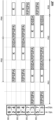
- FIG. 20 is a timing chart showing the operation of the solid-state imaging device according to the sixth embodiment. Note that R indicates the reset period, PS indicates the P-phase settling period, PA indicates the P-phase AD conversion period, K indicates the transfer period from the capacitor to the floating diffusion, DS indicates the D-phase settling period, and DA indicates the D-phase AD conversion period.
- the P-phase pixel signal and the D-phase pixel signal are sequentially read out from the first pixel of each of the 4-pixel shared cells CEL1 and CEL2, and are sequentially transmitted via each vertical signal line VSL1 and VSL2.
- the P-phase pixel signal and the D-phase pixel signal are sequentially read out from the first pixel of each of the 4-pixel shared cells CEL3 and CEL4, and are sequentially transmitted via each of the vertical signal lines VSL1 and VSL2.
- the reset period R, the P-phase settling period PS, and the P-phase AD conversion period PA for the first pixel of each of the 4-pixel shared cells CEL3 and CEL4 overlap with the transfer period K for the first pixel of each of the 4-pixel shared cells CEL1 and CEL2.
- the P-phase pixel signal and the D-phase pixel signal are sequentially read out from the second pixel of each of the four-pixel shared cells CEL1, CEL2, and sequentially transmitted via each of the vertical signal lines VSL1, VSL2.
- the reset period R, the P-phase settling period PS, and the P-phase AD conversion period PA for the second pixel of each of the four-pixel shared cells CEL1, CEL2 overlap with the transfer period K for the first pixel of each of the four-pixel shared cells CEL3, CEL4.
- the P-phase pixel signal and the D-phase pixel signal are sequentially read out from the second pixel of each of the four-pixel shared cells CEL3 and CEL4, and are sequentially transmitted via each of the vertical signal lines VSL1 and VSL2.
- the reset period R, the P-phase settling period PS, and the P-phase AD conversion period PA for the second pixel of each of the four-pixel shared cells CEL3 and CEL4 overlap with the transfer period K for the second pixel of each of the four-pixel shared cells CEL1 and CEL2.
- the P-phase pixel signal and the D-phase pixel signal are sequentially read out from the third pixel of each of the four-pixel shared cells CEL1, CEL2, and sequentially transmitted via each of the vertical signal lines VSL1, VSL2.
- the reset period R, the P-phase settling period PS, and the P-phase AD conversion period PA for the third pixel of each of the four-pixel shared cells CEL1, CEL2 overlap with the transfer period K for the second pixel of each of the four-pixel shared cells CEL3, CEL4.
- pixel signals read from pixels in different rows in the same column are AD converted in a time-division manner. This makes it possible to suppress an increase in the size of pixels to which a charge domain is applied, while eliminating the need for a waiting period before AD conversion for pixels in different rows in the same column.
- the reset period R, the P-phase settling period PS, and the P-phase AD conversion period PA of the 4-pixel shared cells CEL in different rows in the same column are overlapped with the transfer period K.
- the reset period R of the 4-pixel shared cells CEL in different rows in the same column is prevented from overlapping with the transfer period K.
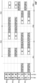
- FIG. 21 is a timing chart showing the operation of the solid-state imaging device according to the seventh embodiment.
- the configuration and readout order of the four-pixel shared cell CEL in the seventh embodiment are the same as those of the four-pixel shared cell CEL in the sixth embodiment.
- the P-phase settling period PS and the P-phase AD conversion period PA of the four-pixel shared cells CEL in different rows in the same column overlap with the transfer period K, but the reset period R does not overlap with the transfer period K.
- the selection signal SEL for each row it is not necessary to prepare a P-phase mode and a D-phase mode, and since the reset mode row and the transfer mode row do not exist at the same time, it can be treated as a common mode.
- the reset period R does not overlap with the transfer period K, the time required for the reset period R is added to the time required for the transfer period K.
- the reset period R of the four-pixel shared cells CEL in different rows in the same column is prevented from overlapping with the transfer period K. This eliminates the need to provide a P-phase mode and a D-phase mode, and also makes it possible to prevent rows in the reset mode and rows in the transfer mode from existing at the same time, simplifying the read control.
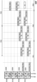
- FIG. 22 is a timing chart showing the operation of the solid-state imaging device according to the eighth embodiment.
- the 2-pixel shared cells CEA1 to CEA4, CEB1 to CEB4 are arranged in a matrix along the row and column directions.
- pixels can be arranged in a 1x2 array.
- the 2-pixel shared cells in the same column are connected to the same vertical signal lines VSL1 to VSLn, and the 2-pixel shared cells in different columns are connected to different vertical signal lines VSL1 to VSLn.
- the 2-pixel shared cells CEA1 to CEA4 in the same column are connected to the vertical signal line VSL1
- the 2-pixel shared cells CEB1 to CEB4 in the same column are connected to the vertical signal line VSL2.
- pixel signals are simultaneously read out from the first pixel of the two-pixel shared cells CEA1 and CEA2 to the vertical signal lines VSL1 and VSL2, and then pixel signals are simultaneously read out from the first pixel of the two-pixel shared cells CEB1 and CEB2 to the vertical signal lines VSL1 and VSL2. Furthermore, pixel signals are simultaneously read out from the second pixel of the two-pixel shared cells CEA1 and CEA2 to the vertical signal lines VSL1 and VSL2, and then pixel signals are simultaneously read out from the second pixel of the two-pixel shared cells CEB1 and CEB2 to the vertical signal lines VSL1 and VSL2.
- pixel signals are simultaneously read out from the first pixels of the two-pixel sharing cells CEA3 and CEA4 to the vertical signal lines VSL1 and VSL2, and then pixel signals are simultaneously read out from the first pixels of the two-pixel sharing cells CEB3 and CEB4 to the vertical signal lines VSL1 and VSL2. Furthermore, pixel signals are simultaneously read out from the second pixels of the two-pixel sharing cells CEA3 and CEA4 to the vertical signal lines VSL1 and VSL2, and then pixel signals are simultaneously read out from the second pixels of the two-pixel sharing cells CEB3 and CEB4 to the vertical signal lines VSL1 and VSL2.
- pixel signals are read out from each pixel of the two-pixel sharing cells CEA1, CEA2, CEB1, and CEB2 in the order of 1 ⁇ 2 ⁇ 3 ⁇ 4, and then pixel signals are read out from each pixel of the two-pixel sharing cells CEA3, CEA4, CEB3, and CEB4 in the order of 5 ⁇ 6 ⁇ 7 ⁇ 8.
- CEA1, CEA2, CEB1, and CEB2 there is no back and forth movement in the column direction between the two-pixel sharing cells CEA1, CEA2, CEB1, and CEB2.
- the P-phase pixel signal and the D-phase pixel signal are sequentially read out from the first pixel of each of the 2-pixel sharing cells CEA1 and CEA2, and are sequentially transmitted via each vertical signal line VSL1 and VSL2.
- the P-phase pixel signal and the D-phase pixel signal are sequentially read out from the second pixel of each of the 2-pixel shared cells CEA1, CEA2, and sequentially transmitted via each of the vertical signal lines VSL1, VSL2.
- the P-phase settling period PS and the P-phase AD conversion period PA for the second pixel of each of the 2-pixel shared cells CEA1, CEA2 overlap with the transfer period K for the first pixel of each of the 2-pixel shared cells CEA1, CEA2.
- the reset period R for the second pixel of each of the 2-pixel shared cells CEA1, CEA2 does not overlap with the transfer period K for the first pixel of each of the 2-pixel shared cells CEA1, CEA2.
- the P-phase pixel signal and the D-phase pixel signal are sequentially read out from the second pixel of each of the 2-pixel sharing cells CEB1, CEB2, and sequentially transmitted via each of the vertical signal lines VSL1, VSL2.
- the P-phase settling period PS and the P-phase AD conversion period PA for the second pixel of each of the 2-pixel sharing cells CEB1, CEB2 overlap with the transfer period K for the first pixel of each of the 2-pixel sharing cells CEB1, CEB2.
- the reset period R for the second pixel of each of the 2-pixel sharing cells CEB1, CEB2 does not overlap with the transfer period K for the first pixel of each of the 2-pixel sharing cells CEB1, CEB2.
- the P-phase pixel signal and the D-phase pixel signal are sequentially read out from the first pixel of each of the four-pixel shared cells CEL1, CEL2, and sequentially transmitted via each of the vertical signal lines VSL1, VSL2.
- the reset period R of the first pixel of each of the four-pixel shared cells CEL3, CEL4 is carried out ahead of the readout period PX1.
- the reset period R for the first pixel of each of the four-pixel shared cells CEL3, CEL4 does not overlap with the transfer period K for the first pixel of each of the four-pixel shared cells CEL1, CEL2.
- the reset period R for the first pixel of each of the four-pixel shared cells CEL5 and CEL6 overlaps with the D-phase AD conversion period DA for the first pixel of each of the four-pixel shared cells CEL1 and CEL2, and does not overlap with the transfer period K for the first pixel of each of the four-pixel shared cells CEL3 and CEL4.
- the P-phase pixel signal and the D-phase pixel signal are sequentially read out from the first pixel of each of the four-pixel shared cells CEL5 and CEL6, and are sequentially transmitted via the vertical signal lines VSL1 and VSL2.
- the reset period R of the second pixel of each of the four-pixel shared cells CEL1 and CEL2 is carried out ahead of the readout period PX3.
- the P-phase settling period PS and the P-phase AD conversion period PA for the first pixel of each of the four-pixel shared cells CEL5 and CEL6 overlap with the transfer period K for the first pixel of each of the four-pixel shared cells CEL3 and CEL4.
- the reset period R for the second pixel of each of the four-pixel shared cells CEL3 and CEL4 overlaps with the D-phase AD conversion period DA for the second pixel of each of the four-pixel shared cells CEL1 and CEL2, and does not overlap with the transfer period K for the second pixel of each of the four-pixel shared cells CEL1 and CEL2.
- the P-phase pixel signal and the D-phase pixel signal are sequentially read out from the second pixel of each of the four-pixel shared cells CEL3 and CEL4, and are sequentially transmitted via each vertical signal line VSL1 and VSL2.
- the reset period R of the 4-pixel shared cells in different rows in the same column does not overlap with the transfer period K, but overlaps with the D-phase AD conversion period DA. This allows the reset period R to be brought forward during the D-phase AD conversion period DA of the 4-pixel shared cells in different rows in the same column, thereby speeding up readout from the 4-pixel shared cells.
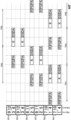
- FIG. 24 is a timing chart showing the operation of the solid-state imaging device according to the tenth embodiment.
- pixel signals are simultaneously read out from the first pixels of two-pixel shared cells CEA1 and CEA2 to vertical signal lines VSL1 and VSL2, and then pixel signals are simultaneously read out from the first pixels of two-pixel shared cells CEA3 and CEA4 to vertical signal lines VSL1 and VSL2. Furthermore, pixel signals are simultaneously read out from the first pixels of two-pixel shared cells CEB1 and CEB2 to vertical signal lines VSL1 and VSL2, and then pixel signals are simultaneously read out from the first pixels of two-pixel shared cells CEB3 and CEB4 to vertical signal lines VSL1 and VSL2.
- pixel signals are simultaneously read out from the second pixels of the two-pixel sharing cells CEA1 and CEA2 to the vertical signal lines VSL1 and VSL2, and then pixel signals are simultaneously read out from the second pixels of the two-pixel sharing cells CEA3 and CEA4 to the vertical signal lines VSL1 and VSL2. Furthermore, pixel signals are simultaneously read out from the second pixels of the two-pixel sharing cells CEB1 and CEB2 to the vertical signal lines VSL1 and VSL2, and then pixel signals are simultaneously read out from the second pixels of the two-pixel sharing cells CEB3 and CEB4 to the vertical signal lines VSL1 and VSL2. At this time, pixel signals are read out from the pixels of the two-pixel sharing cells CEA1 to CEA4 and CEB1 to CEB4 in the order of 1 ⁇ 2 ⁇ 3 ⁇ 4 ⁇ 5 ⁇ 6 ⁇ 7 ⁇ 8.
- the P-phase pixel signal and the D-phase pixel signal are sequentially read out from the first pixel of each of the 2-pixel shared cells CEA3, CEA4, and sequentially transmitted via each of the vertical signal lines VSL1, VSL2.
- the reset period R of the first pixel of each of the 2-pixel shared cells CEB1, CEB2 is carried out ahead of the readout period PX2.
- the P-phase settling period PS and the P-phase AD conversion period PA for the first pixel of each of the 2-pixel shared cells CEA3, CEA4 overlap with the transfer period K for the first pixel of each of the 2-pixel shared cells CEA1, CEA2.
- the reset period R for the first pixel of each of the two-pixel shared cells CEB1 and CEB2 overlaps with the D-phase AD conversion period DA for the first pixel of each of the two-pixel shared cells CEA1 and CEA2, but does not overlap with the transfer period K for the first pixel of each of the two-pixel shared cells CEA3 and CEA4.
- the reset period R for the first pixel of each of the two-pixel shared cells CEB3 and CEB4 overlaps with the D-phase AD conversion period DA for the first pixel of each of the two-pixel shared cells CEA3 and CEA4, but does not overlap with the transfer period K for the first pixel of each of the two-pixel shared cells CEB1 and CEB2.
- the P-phase pixel signal and the D-phase pixel signal are sequentially read out from the first pixel of each of the 2-pixel shared cells CEB3, CEB4, and sequentially transmitted via each of the vertical signal lines VSL1, VSL2.
- the reset period R of the second pixel of each of the 2-pixel shared cells CEA1, CEA2 is carried out ahead of the readout period PX4.
- the P-phase settling period PS and the P-phase AD conversion period PA for the first pixel of each of the 2-pixel shared cells CEB3, CEB4 overlap with the transfer period K for the first pixel of each of the 2-pixel shared cells CEB1, CEB2.
- the reset period R for the second pixel of each of the two-pixel shared cells CEA1 and CEA2 overlaps with the D-phase AD conversion period DA for the first pixel of each of the two-pixel shared cells CEB1 and CEB2, but does not overlap with the transfer period K for the first pixel of each of the two-pixel shared cells CEB3 and CEB4.
- the P-phase pixel signal and the D-phase pixel signal are sequentially read out from the second pixel of each of the 2-pixel sharing cells CEA1 and CEA2, and are sequentially transmitted via each vertical signal line VSL1 and VSL2.
- the reset period R of the 2-pixel shared cell in a different row in the same column is made not to overlap with the transfer period K, but overlaps with the D-phase AD conversion period DA.
- the reset period R in the case of a 4-pixel shared cell, three 4-pixel shared cells adjacent in the column direction are spanned during readout, whereas in the case of a 2-pixel shared cell, it is sufficient to span two 2-pixel shared cells adjacent in the column direction during readout. This makes it possible to suppress an increase in the time lag until readout from each pixel of each 2-pixel shared cell is completed while speeding up readout from the 2-pixel shared cell.
- FIG. 25 is a diagram showing the pixel readout order of the solid-state imaging device according to the eleventh embodiment. Note that this figure shows an example in which AD conversion is put on hold during the transfer period of the charges held in the capacitors of each of the four-pixel shared cells CEL1 to CEL4.
- the pixel read order is set in the same way as in the sixth embodiment described above.
- pixel signals are read out from each pixel of the four-pixel shared cells CEL1 to CEL4 while straddling two four-pixel shared cells CEL1 to CEL4 adjacent to each other in the column direction.
- pixel signals are simultaneously read out from the first pixels of the four-pixel shared cells CEL1 and CEL2 to the vertical signal lines VSL1 and VSL2, and then pixel signals are simultaneously read out from the second pixels of the four-pixel shared cells CEL1 and CEL2 to the vertical signal lines VSL1 and VSL2. Furthermore, pixel signals are simultaneously read out from the third pixels of the four-pixel shared cells CEL1 and CEL2 to the vertical signal lines VSL1 and VSL2, and then pixel signals are simultaneously read out from the fourth pixels of the four-pixel shared cells CEL1 and CEL2 to the vertical signal lines VSL1 and VSL2.
- pixel signals are simultaneously read out from the first pixels of the four-pixel shared cells CEL3 and CEL4 to the vertical signal lines VSL1 and VSL2, and then pixel signals are simultaneously read out from the second pixels of the four-pixel shared cells CEL3 and CEL4 to the vertical signal lines VSL1 and VSL2. Furthermore, pixel signals are simultaneously read out from the third pixels of the four-pixel shared cells CEL3 and CEL4 to the vertical signal lines VSL1 and VSL2, and then pixel signals are simultaneously read out from the fourth pixels of the four-pixel shared cells CEL3 and CEL4 to the vertical signal lines VSL1 and VSL2.
- pixel signals are read out from the pixels of the four-pixel shared cells CEL1 and CEL2 in the order of 1 ⁇ 2 ⁇ 3 ⁇ 4, and then pixel signals are read out from the pixels of the four-pixel shared cells CEL3 and CEL4 in the order of 5 ⁇ 6 ⁇ 7 ⁇ 8.
- FIG. 26 is a timing chart showing the operation of a solid-state imaging device according to the eleventh embodiment. Note that the figure shows an example in which AD conversion is put on hold during the transfer period of the charges held in the capacitors of each of the four-pixel shared cells CEL1 to CEL4.
- the process of performing AD conversion overlapping with the transfer period of the charges held in the capacitors of each of the four-pixel shared cells CEL1 to CEL4 operates with the same timing as in the sixth embodiment described above, as shown in FIG. 20.
- the P-phase pixel signal and the D-phase pixel signal are sequentially read out from the first pixel of each of the 4-pixel shared cells CEL1, CEL2, and sequentially transmitted via each of the vertical signal lines VSL1, VSL2.
- the reset period R, P-phase settling period PS, and P-phase AD conversion period PA for the first pixel of each of the 4-pixel shared cells CEL1, CEL2 do not overlap with the transfer period K for the first pixel of each of the 4-pixel shared cells CEL1, CEL2.
- the P-phase pixel signal and the D-phase pixel signal are sequentially read out from the second pixel of each of the 4-pixel shared cells CEL1, CEL2, and sequentially transmitted via each of the vertical signal lines VSL1, VSL2.
- the reset period R, the P-phase settling period PS, and the P-phase AD conversion period PA for the second pixel of each of the 4-pixel shared cells CEL1, CEL2 do not overlap with the transfer period K for the second pixel of each of the 4-pixel shared cells CEL1, CEL2.
- the P-phase pixel signal and the D-phase pixel signal are sequentially read out from the third pixel of each of the four-pixel shared cells CEL1, CEL2, and sequentially transmitted via each of the vertical signal lines VSL1, VSL2.
- the reset period R, the P-phase settling period PS, and the P-phase AD conversion period PA for the third pixel of each of the four-pixel shared cells CEL1, CEL2 do not overlap with the transfer period K for the third pixel of each of the four-pixel shared cells CEL1, CEL2.
- FIG. 27 is a timing chart showing an example of the operation of the AD conversion unit for one column of the solid-state imaging device according to the eleventh embodiment. Note that this figure shows an example in which AD conversion is put on hold during the transfer period of the charges held in the capacitors of each of the four-pixel shared cells CEL1 to CEL4.
- the comparator CM' of the fourth embodiment described above is used in the process of putting AD conversion on hold during the transfer period of the charge held in the capacitor of each of the four-pixel shared cells CEL1 to CEL4. At this time, only one of the two pixel signal inputs of the comparator CM' is used. At this time, the auto-zero switches SW2A, SW2B and the switches SW12A, SW12B can be always off.
- Comparator CM1 is in use during the period AK between the current P-phase AD conversion period PA and the D-phase AD conversion period DA.
- FIG. 28 is a timing chart showing the operation of the CDS process of the solid-state imaging device according to the eleventh embodiment. Note that the figure shows an example in which AD conversion is put on hold during the transfer period of the charges held in the capacitors of each of the four-pixel shared cells CEL1 to CEL4.
- a P-phase count period CT1 is provided in the P-phase AD conversion period PA of each pixel of the four-pixel shared cells CEL1, CEL2.
- a D-phase count period CT3 is provided in the D-phase AD conversion period DA of each pixel of the four-pixel shared cells CEL1, CEL2.
- the P-phase AD conversion result PN1 is stored in the P-phase register 161 (ST1).
- the D-phase count period CT3 of each pixel of the four-pixel shared cells CEL1, CEL2 is completed, CDS calculation is performed, and the CDS processing result CS1 is stored in the output register 164 (ST3).
- a readout period RD of each CDS processing result CS1 is set during the storage timing ST3 of each CDS processing result CS1.
- the solid-state imaging device includes semiconductor chips 921 and 922.
- Semiconductor chip 922 is stacked on semiconductor chip 921.
- a pixel array section 923 is formed in the semiconductor chip 922.
- pixels 931 are arranged in a matrix in the row and column directions.
- the pixels 931 may be pixels PIX1 and PIX2 as shown in FIG. 3, a four-pixel shared cell CEL as shown in FIG. 18, or a two-pixel shared cell CEL as shown in FIG. 22.
- a pad electrode 932 and a via electrode 933 are formed around the pixel array section 923.
- the via electrode 933 passes through the semiconductor chip 922 and can electrically connect the semiconductor chips 921 and 922 to each other.
- a peripheral circuit 924 is formed on the semiconductor chip 921.
- a column readout circuit 925, a column ADC 926, a communication interface 927, and an oscillator circuit 928 are formed on the peripheral circuit 924.
- the column readout circuit 925 and the column ADC 926 may be formed to correspond to positions on both sides of the pixel array unit 923 in the column direction.
- the column ADC 926 can be provided with an AD conversion unit according to any one of the first to eleventh embodiments described above.
- the semiconductor chips 921 and 922 may be directly bonded. Hybrid bonding may be used for directly bonding the semiconductor chips 921 and 922. In this case, the semiconductor chips 921 and 922 may be electrically connected based on a Cu-Cu connection.
- the material of the semiconductor substrate used for the semiconductor chips 921 and 922 may be Si, InGaAs, or InP.
- the semiconductor chip 922 in which the pixel array section 923 is formed is stacked on the semiconductor chip 921 in which the peripheral circuit 924 is formed. This makes it possible to increase the sensitivity of the solid-state imaging device while suppressing an increase in the mounting area of the semiconductor chip in which the solid-state imaging device is formed.
- FIG. 30 is a block diagram showing a schematic configuration example of a vehicle control system, which is an example of a mobile object control system to which the technology disclosed herein can be applied.
- the vehicle control system 12000 includes a plurality of electronic control units connected via a communication network 12001.
- the vehicle control system 12000 includes a drive system control unit 12010, a body system control unit 12020, an outside vehicle information detection unit 12030, an inside vehicle information detection unit 12040, and an integrated control unit 12050.
- Also shown as functional components of the integrated control unit 12050 are a microcomputer 12051, an audio/video output unit 12052, and an in-vehicle network I/F (interface) 12053.
- the drive system control unit 12010 controls the operation of devices related to the drive system of the vehicle according to various programs.
- the drive system control unit 12010 functions as a control device for a drive force generating device for generating the drive force of the vehicle, such as an internal combustion engine or a drive motor, a drive force transmission mechanism for transmitting the drive force to the wheels, a steering mechanism for adjusting the steering angle of the vehicle, and a braking device for generating a braking force for the vehicle.
- the imaging unit 12031 is an optical sensor that receives light and outputs an electrical signal according to the amount of light received.
- the imaging unit 12031 can output the electrical signal as an image, or as distance measurement information.
- the light received by the imaging unit 12031 may be visible light, or may be invisible light such as infrared light.
- the in-vehicle information detection unit 12040 detects information inside the vehicle.
- a driver state detection unit 12041 that detects the state of the driver is connected.
- the driver state detection unit 12041 includes, for example, a camera that captures an image of the driver, and the in-vehicle information detection unit 12040 may calculate the driver's degree of fatigue or concentration based on the detection information input from the driver state detection unit 12041, or may determine whether the driver is dozing off.
- the microcomputer 12051 can calculate control target values for the driving force generating device, steering mechanism, or braking device based on information inside and outside the vehicle acquired by the outside vehicle information detection unit 12030 or the inside vehicle information detection unit 12040, and output control commands to the drive system control unit 12010.
- the microcomputer 12051 can perform cooperative control aimed at realizing the functions of an Advanced Driver Assistance System (ADAS), including vehicle collision avoidance or impact mitigation, following driving based on the distance between vehicles, maintaining vehicle speed, vehicle collision warning, or vehicle lane departure warning.
- ADAS Advanced Driver Assistance System
- the microcomputer 12051 can also perform cooperative control for the purpose of autonomous driving, which allows the vehicle to travel autonomously without relying on the driver's operation, by controlling the driving force generating device, steering mechanism, braking device, etc. based on information about the surroundings of the vehicle acquired by the outside vehicle information detection unit 12030 or the inside vehicle information detection unit 12040.
- the microcomputer 12051 can also output control commands to the body system control unit 12020 based on information outside the vehicle acquired by the outside-vehicle information detection unit 12030. For example, the microcomputer 12051 can control the headlamps according to the position of a preceding vehicle or an oncoming vehicle detected by the outside-vehicle information detection unit 12030, and perform cooperative control aimed at preventing glare, such as switching from high beams to low beams.
- the audio/image output unit 12052 transmits at least one output signal of audio and image to an output device capable of visually or audibly notifying the occupants of the vehicle or the outside of the vehicle of information.
- an audio speaker 12061, a display unit 12062, and an instrument panel 12063 are exemplified as output devices.
- the display unit 12062 may include, for example, at least one of an on-board display and a head-up display.
- FIG. 31 shows an example of the installation position of the imaging unit 12031.
- the imaging unit 12031 includes imaging units 12101, 12102, 12103, 12104, and 12105.
- the imaging units 12101, 12102, 12103, 12104, and 12105 are provided, for example, at the front nose, side mirrors, rear bumper, back door, and upper part of the windshield inside the vehicle cabin of the vehicle 12100.
- the imaging unit 12101 provided at the front nose and the imaging unit 12105 provided at the upper part of the windshield inside the vehicle cabin mainly acquire images of the front of the vehicle 12100.
- the imaging units 12102 and 12103 provided at the side mirrors mainly acquire images of the sides of the vehicle 12100.
- the imaging unit 12104 provided at the rear bumper or back door mainly acquires images of the rear of the vehicle 12100.
- the imaging unit 12105 provided at the upper part of the windshield inside the vehicle cabin is mainly used to detect leading vehicles, pedestrians, obstacles, traffic lights, traffic signs, lanes, etc.
- FIG. 31 shows an example of the imaging ranges of the imaging units 12101 to 12104.
- Imaging range 12111 indicates the imaging range of the imaging unit 12101 provided on the front nose
- imaging ranges 12112 and 12113 indicate the imaging ranges of the imaging units 12102 and 12103 provided on the side mirrors, respectively
- imaging range 12114 indicates the imaging range of the imaging unit 12104 provided on the rear bumper or back door.
- an overhead image of the vehicle 12100 viewed from above is obtained by superimposing the image data captured by the imaging units 12101 to 12104.
- the microcomputer 12051 can obtain the distance to each solid object within the imaging ranges 12111 to 12114 and the change in this distance over time (relative speed with respect to the vehicle 12100) based on the distance information obtained from the imaging units 12101 to 12104, and can extract as a preceding vehicle, in particular, the closest solid object on the path of the vehicle 12100 that is traveling in approximately the same direction as the vehicle 12100 at a predetermined speed (e.g., 0 km/h or faster). Furthermore, the microcomputer 12051 can set the inter-vehicle distance that should be maintained in advance in front of the preceding vehicle, and perform automatic braking control (including follow-up stop control) and automatic acceleration control (including follow-up start control). In this way, cooperative control can be performed for the purpose of automatic driving, which runs autonomously without relying on the driver's operation.
- automatic braking control including follow-up stop control
- automatic acceleration control including follow-up start control
- the microcomputer 12051 classifies and extracts three-dimensional object data on three-dimensional objects, such as two-wheeled vehicles, ordinary vehicles, large vehicles, pedestrians, utility poles, and other three-dimensional objects, based on the distance information obtained from the imaging units 12101 to 12104, and can use the data to automatically avoid obstacles.
- the microcomputer 12051 distinguishes obstacles around the vehicle 12100 into obstacles that are visible to the driver of the vehicle 12100 and obstacles that are difficult to see.
- the microcomputer 12051 determines the collision risk, which indicates the risk of collision with each obstacle, and when the collision risk is equal to or exceeds a set value and there is a possibility of a collision, it can provide driving assistance for collision avoidance by outputting an alarm to the driver via the audio speaker 12061 or the display unit 12062, or by forcibly decelerating or steering to avoid a collision via the drive system control unit 12010.
- At least one of the imaging units 12101 to 12104 may be an infrared camera that detects infrared rays.
- the microcomputer 12051 can recognize a pedestrian by determining whether or not a pedestrian is present in the captured image of the imaging units 12101 to 12104. The recognition of such a pedestrian is performed, for example, by a procedure of extracting feature points in the captured image of the imaging units 12101 to 12104 as infrared cameras, and a procedure of performing pattern matching processing on a series of feature points that indicate the contour of an object to determine whether or not it is a pedestrian.
- the audio/image output unit 12052 controls the display unit 12062 to superimpose a rectangular contour line for emphasis on the recognized pedestrian.
- the audio/image output unit 12052 may also control the display unit 12062 to display an icon or the like indicating a pedestrian at a desired position.
- the technology disclosed herein can be applied to the imaging unit 12031 of the configuration described above.
- the imaging device of the above-mentioned embodiment can be applied to the imaging unit 12031.
- the present technology can also be configured as follows. (1) a pixel capable of transferring and holding photoelectrically converted electric charges; and an AD conversion unit capable of switching, in a time-division manner, AD (Analog to Digital) conversion of pixel signals read out from pixels in different rows in the same column.
- the pixel is A photoelectric conversion unit; a capacitor for holding charges photoelectrically converted by the photoelectric conversion unit; a first transfer transistor that transfers the charge photoelectrically converted by the photoelectric conversion unit to the capacitor; a second transfer transistor that transfers the charge held in the capacitor to a floating diffusion; an output transistor that outputs the pixel signal based on the charge transferred to the floating diffusion; and a selection transistor for selecting an output of the pixel signal.
- the AD conversion unit The imaging device described in (2) performs AD conversion of a pixel signal read out from a second pixel in a second row in a first column during an AD conversion period that overlaps with a transfer period in which charge held in a capacitor of a first pixel in a first row in a first column is transferred to a floating diffusion.
- the imaging device according to (3) further comprising: a second comparator whose input is connected to the vertical signal line.
- the AD conversion of the second comparator is put on hold;
- the imaging device according to (5) wherein the AD conversion by the first comparator is put on hold during the AD conversion by the second comparator.
- a vertical signal line for transmitting the pixel signal in a column direction; a comparator having an input connected to the vertical signal line; a first switch connected between the input of the comparator and the vertical signal line;
- the imaging device according to (3) further comprising a second switch connected between the input of the comparator and the vertical signal line.
- a vertical signal line for transmitting the pixel signal in a column direction; a comparator having a first input and a second input connected to the vertical signal line;
- the comparator is A first transistor; A second transistor; a third transistor capable of forming a differential pair with each of the first transistor and the second transistor; a fourth transistor capable of forming a differential pair with each of the first transistor and the second transistor; a first switch connected in series with the first transistor; a second switch connected in series with the second transistor; a third switch connected in series with the third transistor;
- the imaging device according to (3) further comprising: a fourth switch connected in series to the fourth transistor.
- (10) a first capacitor connected in series to a gate of the first transistor; a second capacitor connected in series to the gate of the second transistor; a third capacitor connected in series to the gate of the third transistor; a fourth capacitor connected in series to the gate of the fourth transistor; a first auto-zero switch connected between the gate of the first transistor and the first switch; a second auto-zero switch connected between the gate of the second transistor and the second switch; a third auto-zero switch connected between the gate and drain of the third transistor;
- the imaging device described in (9) further comprising a fourth auto-zero switch connected between the gate and drain of the fourth transistor.
- a first P-phase register that holds a P-phase AD conversion result of a pixel signal read out from the first pixel
- a second P-phase register that holds a P-phase AD conversion result of a pixel signal read out from the second pixel
- a CDS processing unit that performs a first CDS (Correlated Double Sampling) process based on the
- the imaging device according to any one of (1) to (12), wherein the pixel transfers and holds the photoelectrically converted electric charge based on a global shutter operation.
- (14) a first transistor; A second transistor; a third transistor capable of forming a differential pair with each of the first transistor and the second transistor; a fourth transistor capable of forming a differential pair with each of the first transistor and the second transistor; a first switch connected in series with the first transistor; a second switch connected in series with the second transistor; a third switch connected in series with the third transistor; a fourth switch connected in series with the fourth transistor.
- a first capacitor is connected in series to a gate of the first transistor; a second capacitor is connected in series to the gate of the second transistor; a third capacitor is connected in series to the gate of the third transistor; a fourth capacitor is connected in series to the gate of the fourth transistor; a first auto-zero switch connected between the gate of the first transistor and the first switch; a second auto-zero switch connected between the gate of the second transistor and the second switch; a third auto-zero switch connected between the gate and the drain of the third transistor;
- a first pixel in a first row in a first column transfers the photoelectrically converted charge to a capacitor in the first pixel and holds the charge;
- a second pixel in a second row in a first column transfers the photoelectrically converted charge to a capacitor in the second pixel and holds the charge;
- an AD conversion unit performing AD conversion on a pixel signal read out from the second pixel during an AD conversion period that overlaps with a transfer period during which charge held in a capacitor of the first pixel is transferred to a floating diffusion;
- Imaging device 101 Optical system 102 Solid-state imaging device 103 Imaging control unit 104 Image processing unit 105 Memory unit 106 Display unit 107 Operation unit 108 Bus 111 Pixel array unit 112 Vertical scanning circuit 113 Column readout circuit 114 Column signal processing unit 115 Horizontal scanning circuit 116 Control circuit PIX1, PIX2 Pixel HSL Horizontal drive line VSL Vertical signal line PD1, PD2 Photodiode FD1, FD2 Floating diffusion CA1, CA2 Capacitor 122, 222 Overflow control transistor 123, 124, 223, 224 Transfer transistor 125, 225 Reset transistor 126, 226 Output transistor 127, 227 Selection transistor 131-1 to 131-3: Comparison section 132-1 to 132-3: Counter
Landscapes
- Engineering & Computer Science (AREA)
- Multimedia (AREA)
- Signal Processing (AREA)
- Transforming Light Signals Into Electric Signals (AREA)
Abstract
フレームレートの低下を抑制しつつ、キャパシタからフローティングディフュージョンに電荷を転送可能とする。 撮像装置は、光電変換した電荷を転送して保持可能な画素と、同一カラムで異なるロウの画素から読み出された画素信号のAD(Analog to Digital)変換を時分割的に切替可能なAD変換部とを備える。画素は、光電変換部と、光電変換部にて光電変換された電荷を保持するキャパシタと、光電変換部にて光電変換された電荷をキャパシタに転送する第1転送トランジスタと、キャパシタに保持された電荷をフローティングディフュージョンに転送する第2転送トランジスタと、フローティングディフュージョンに転送された電荷に基づいて画素信号を出力する出力トランジスタと、画素信号の出力を選択する選択トランジスタとを備えてもよい。
Description
本技術は、撮像装置、コンパレータおよび撮像方法に関する。詳しくは、本技術は、光電変換した電荷を転送して画素に保持可能な撮像装置、コンパレータおよび撮像方法に関する。
グローバルシャッタでは、光電変換部から転送された電荷を保持するキャパシタが画素に設けられる。例えば、光電変換部から転送された電荷を保持するキャパシタを含む画素と、キャパシタから電荷が転送されるフローティングディフュージョンが設けられた撮像装置が提案されている(例えば、特許文献1参照)。
しかしながら、上述の従来技術では、キャパシタからフローティングディフュージョンへの電荷の転送期間中は、画素信号のAD変換が行ごとに待機され、フレームレートの低下を招くおそれがあった。
本技術はこのような状況に鑑みて生み出されたものであり、フレームレートの低下を抑制しつつ、キャパシタからフローティングディフュージョンに電荷を転送可能とすることを目的とする。
本技術は、上述の問題点を解消するためになされたものであり、その第1の側面は、光電変換した電荷を転送して保持可能な画素と、同一カラムで異なるロウの画素から読み出された画素信号のAD(Analog to Digital)変換を時分割的に切替可能なAD変換部とを備える撮像装置である。これにより、同一カラムの第1画素および第2画素についてAD変換前の待機期間を設けることなく、第1画素および第2画素のそれぞれから読み出された画素信号がAD変換されるという作用をもたらす。
また、第1の側面において、前記画素は、光電変換部と、前記光電変換部にて光電変換された電荷を保持するキャパシタと、前記光電変換部にて光電変換された電荷を前記キャパシタに転送する第1転送トランジスタと、前記キャパシタに保持された電荷をフローティングディフュージョンに転送する第2転送トランジスタと、前記フローティングディフュージョンに転送された電荷に基づいて前記画素信号を出力する出力トランジスタと、前記画素信号の出力を選択する選択トランジスタとを備えてもよい。これにより、光電変換した電荷を転送して保持可能な画素が構成されるという作用をもたらす。
また、第1の側面において、前記AD変換部は、第1カラムで第1ロウの第1画素のキャパシタに保持された電荷がフローティングディフュージョンに転送される転送期間と重複するAD変換期間に前記第1カラムで第2ロウの第2画素から読み出された画素信号のAD変換を実施してもよい。これにより、第1画素での電荷の転送中に第1画素と同一カラムの第2画素から読み出された画素信号がAD変換されるという作用をもたらす。
また、第1の側面において、前記画素信号をカラム方向に伝送する垂直信号線と、前記垂直信号線に入力が接続される第1コンパレータと、前記垂直信号線に入力が接続される第2コンパレータとを備えてもよい。これにより、2つのコンパレータを用いることで、同一カラムで異なるロウの画素から読み出された画素信号が時分割的にAD変換されるという作用をもたらす。
また、第1の側面において、前記第1コンパレータのオートゼロ動作後に前記第1コンパレータにて前記第1画素から読み出された画素信号のP相のAD変換が実施され、前記第1画素から読み出された画素信号のP相のAD変換の実施後に前記第2コンパレータのオートゼロ動作が実施され、前記第2コンパレータのオートゼロ動作後に前記第2コンパレータにて前記第2画素から読み出された画素信号のP相のAD変換が実施され、前記第2画素から読み出された画素信号のP相のAD変換の実施後に前記第1コンパレータにて前記第1画素から読み出された画素信号のD相のAD変換が実施され、前記第1画素から読み出された画素信号のD相のAD変換の実施後に前記第2コンパレータにて前記第2画素から読み出された画素信号のD相のAD変換が実施されてもよい。これにより、第1コンパレータのオートゼロ動作後に、第1画素から読み出された画素信号のP相およびD相のAD変換が実施され、第2コンパレータのオートゼロ動作後に、第2画素から読み出された画素信号のP相およびD相のAD変換が実施されるという作用をもたらす。
また、第1の側面において、前記第1コンパレータのAD変換中に前記第2コンパレータのAD変換は待機され、前記第2コンパレータのAD変換中に前記第1コンパレータのAD変換は待機されてもよい。これにより、コンパレータの使用状態に応じてコンパレータがアクティブ化されるという作用をもたらす。
また、第1の側面において、前記画素信号をカラム方向に伝送する垂直信号線と、前記垂直信号線に入力が接続されるコンパレータと、前記コンパレータの入力と前記垂直信号線との間に接続された第1スイッチと、前記コンパレータの入力と前記垂直信号線との間に接続された第2スイッチとを備えてもよい。これにより、単一のコンパレータの入力の切替動作に基づいて、同一カラムで異なるロウの画素から読み出された画素信号が時分割的にAD変換されるという作用をもたらす。
また、第1の側面において、前記第1スイッチがオン、前記第2スイッチがオフしているときに、前記第1画素から読み出された画素信号のAD変換が実施され、前記第1スイッチがオフ、前記第2スイッチがオンしているときに、前記第2画素から読み出された画素信号のAD変換が前記コンパレータにて実施されてもよい。これにより、第1画素に保持された電荷の転送中に第2画素から読み出された画素信号のAD変換が実施され、第2画素に保持された電荷の転送中に第1画素から読み出された画素信号のAD変換が実施されるという作用をもたらす。
また、第1の側面において、前記画素信号をカラム方向に伝送する垂直信号線と、前記垂直信号線に第1入力および第2入力が接続されるコンパレータとを備え、前記コンパレータは、第1トランジスタと、第2トランジスタと、前記第1トランジスタおよび前記第2トランジスタのそれぞれと差動対を構成可能な第3トランジスタと、前記第1トランジスタおよび前記第2トランジスタのそれぞれと差動対を構成可能な第4トランジスタと、前記第1トランジスタに直列に接続された第1スイッチと、前記第2トランジスタに直列に接続された第2スイッチと、前記第3トランジスタに直列に接続された第3スイッチと、前記第4トランジスタに直列に接続された第4スイッチとを備えてもよい。これにより、単一のコンパレータの入力の切替動作に起因するチャージインジェクションやフィードスルーの影響を抑制しつつ、同一カラムで異なるロウの画素から読み出された画素信号が時分割的にAD変換されるという作用をもたらす。
また、第1の側面において、前記第1トランジスタのゲートに直列に接続された第1キャパシタと、前記第2トランジスタのゲートに直列に接続された第2キャパシタと、前記第3トランジスタのゲートに直列に接続された第3キャパシタと、前記第4トランジスタのゲートに直列に接続された第4キャパシタと、前記第1トランジスタのゲートと前記第1スイッチとの間に接続された第1オートゼロスイッチと、前記第2トランジスタのゲートと前記第2スイッチとの間に接続された第2オートゼロスイッチと、前記第3トランジスタのゲートとドレインとの間に接続された第3オートゼロスイッチと、前記第4トランジスタのゲートとドレインとの間に接続された第4オートゼロスイッチとを備えてもよい。これにより、単一のコンパレータの入力の切替動作に起因するチャージインジェクションやフィードスルーの影響がキャパシタに伝わるのを抑制しつつ、コンパレータのオートゼロ動作が実現されるという作用をもたらす。
また、第1の側面において、前記第1スイッチおよび前記第3スイッチがオン、前記第2スイッチおよび前記第4スイッチがオフしているときに、前記第1オートゼロスイッチおよび前記第3オートゼロスイッチがオンしてオートゼロ動作が実施された後に前記コンパレータにて前記第1画素から読み出された画素信号のP相のAD変換が実施され、前記第1スイッチおよび前記第3スイッチがオフ、前記第2スイッチおよび前記第4スイッチがオンしているときに、前記第2オートゼロスイッチおよび前記第4オートゼロスイッチがオンしてオートゼロ動作が実施された後に前記コンパレータにて前記第2画素から読み出された画素信号のP相のAD変換が実施され、前記第1スイッチおよび前記第3スイッチがオン、前記第2スイッチおよび前記第4スイッチがオフしているときに、前記コンパレータにて前記第1画素から読み出された画素信号のD相のAD変換が実施され、前記第1スイッチおよび前記第3スイッチがオフ、前記第2スイッチおよび前記第4スイッチがオンしているときに、前記コンパレータにて前記第2画素から読み出された画素信号のD相のAD変換が実施されてもよい。これにより、オートゼロ動作後の単一のコンパレータの入力の切替動作に基づいて、同一カラムで異なるロウの画素から読み出された画素信号が時分割的にAD変換されるという作用をもたらす。
また、第1の側面において、前記第1画素から読み出された画素信号のP相のAD変換結果を保持する第1P相レジスタと、前記第2画素から読み出された画素信号のP相のAD変換結果を保持する第2P相レジスタと、前記第1P相レジスタに保持された前記第1画素から読み出された画素信号のP相のAD変換結果と前記AD変換部から出力された前記第1画素から読み出された画素信号のD相のAD変換結果とに基づいて第1CDS(Correlated Double Sampling)処理を実施し、前記第2P相レジスタに保持された前記第2画素から読み出された画素信号のP相のAD変換結果と前記AD変換部から出力された前記第2画素から読み出された画素信号のD相のAD変換結果とに基づいて第2CDS処理を実施するCDS処理部とをさらに備えてもよい。これにより、チャージドメイン型グローバルシャッタ方式において、同一カラムで異なるロウの画素から読み出された画素信号を時分割的にAD変換しつつ、CDS処理が実現されるという作用をもたらす。
また、第1の側面において、前記画素は、グローバルシャッタ動作に基づいて、前記光電変換した電荷を転送して保持してもよい。これにより、全画素で同時に露光が開始されるという作用をもたらす。
また、第2の側面は、第1トランジスタと、第2トランジスタと、前記第1トランジスタおよび前記第2トランジスタのそれぞれと差動対を構成可能な第3トランジスタと、前記第1トランジスタおよび前記第2トランジスタのそれぞれと差動対を構成可能な第4トランジスタと、前記第1トランジスタに直列に接続された第1スイッチと、前記第2トランジスタに直列に接続された第2スイッチと、前記第3トランジスタに直列に接続された第3スイッチと、前記第4トランジスタに直列に接続された第4スイッチとを備えるコンパレータである。これにより、単一のコンパレータの入力の切替動作に起因するチャージインジェクションやフィードスルーの影響を抑制しつつ、複数の信号が時分割的にAD変換されるという作用をもたらす。
また、第2の側面において、前記第1トランジスタのゲートに第1キャパシタが直列に接続され、前記第2トランジスタのゲートに第2キャパシタが直列に接続され、前記第3トランジスタのゲートに第3キャパシタが直列に接続され、前記第4トランジスタのゲートに第4キャパシタが直列に接続され、前記第1トランジスタのゲートと前記第1スイッチとの間に第1オートゼロスイッチが接続され、前記第2トランジスタのゲートと前記第2スイッチとの間に第2オートゼロスイッチが接続され、前記第3トランジスタのゲートとドレインとの間に第3オートゼロスイッチが接続され、前記第4トランジスタのゲートとドレインとの間に第4オートゼロスイッチが接続されてもよい。これにより、単一のコンパレータの入力の切替動作に起因するチャージインジェクションやフィードスルーの影響がキャパシタに伝わるのを抑制されるという作用をもたらす。
また、第2の側面において、前記第1スイッチおよび前記第3スイッチがオンされる時は、前記第2スイッチおよび前記第4スイッチはオフされ、前記第1スイッチおよび前記第3スイッチがオフされる時は、前記第2スイッチおよび前記第4スイッチはオンされてもよい。これにより、単一のコンパレータの入力の切替動作に基づいて、複数の信号が時分割的にAD変換されるという作用をもたらす。
また、第2の側面において、前記第1スイッチおよび前記第3スイッチがオンされている時に、前記第1オートゼロスイッチおよび前記第3オートゼロスイッチがオンされ、前記第2スイッチおよび前記第4スイッチがオンされている時に、前記第2オートゼロスイッチおよび前記第4オートゼロスイッチがオンされてもよい。これにより、オートゼロ動作後の単一のコンパレータの入力の切替動作に基づいて、複数の信号が時分割的にAD変換されるという作用をもたらす。
また、第2の側面において、前記第1トランジスタのゲートおよび前記第2トランジスタのゲートは、同一の信号線に接続され、前記第3トランジスタのゲートおよび前記第4トランジスタのゲートは、同一の参照信号が入力されてもよい。これにより、同一カラムで異なるロウの画素から読み出された画素信号が時分割的にシングルスロープAD変換されるという作用をもたらす。
また、第3の側面は、第1カラムで第1ロウの第1画素は、光電変換した電荷を前記第1画素内のキャパシタに転送して保持し、第1カラムで第2ロウの第2画素は、光電変換した電荷を前記第2画素内のキャパシタに転送して保持し、AD変換部は、前記第1画素のキャパシタに保持された電荷がフローティングディフュージョンに転送される転送期間と重複するAD変換期間に前記第2画素から読み出された画素信号のAD変換を実施する撮像方法である。これにより、第1画素での電荷の転送中に第1画素と同一カラムの第2画素から読み出された画素信号がAD変換されるという作用をもたらす。
以下、本技術を実施するための形態(以下、実施の形態と称する)について説明する。説明は以下の順序により行う。
1.第1の実施の形態(同一カラムで異なるロウの画素から読み出された画素信号を2つのコンパレータの切替動作に基づいて時分割的にAD変換する例)
2.第2の実施の形態(同一カラムで異なるロウの画素から読み出された画素信号を2つのコンパレータの切替動作に基づいて時分割的にAD変換し、未使用のコンパレータを待機させる例)
3.第3の実施の形態(同一カラムで異なるロウの画素から読み出された画素信号を単一のコンパレータの入力の切替動作に基づいて時分割的にAD変換する例)
4.第4の実施の形態(同一カラムで異なるロウの画素から読み出された画素信号を単一のコンパレータの入力の切替動作に基づいて時分割的にAD変換し、入力を切り替えるスイッチをコンパレータに内蔵した例)
5.第5の実施の形態(同一カラムで異なるロウの画素から読み出された画素信号を単一のコンパレータの入力の切替動作に基づいて時分割的にAD変換し、入力を切り替えるスイッチをコンパレータに内蔵するとともに、参照信号の入力側のオートゼロ動作を省略した例)
6.第6の実施の形態(4画素共有セルの各画素にチャージドメインを適用した例)
7.第7の実施の形態(チャージドメインが適用された4画素共有セルのリセット期間をキャパシタに保持された電荷の転送期間と異ならせた例)
8.第8の実施の形態(チャージドメインが適用された2画素共有セルのリセット期間をキャパシタに保持された電荷の転送期間と異ならせた例)
9.第9の実施の形態(チャージドメインが適用された4画素共有セルのリセット期間をキャパシタに保持された電荷の転送期間と異ならせ、D相AD変換期間と重複させた例)
10.第10の実施の形態(チャージドメインが適用された2画素共有セルのリセット期間をキャパシタに保持された電荷の転送期間と異ならせ、D相AD変換期間と重複させた例)
11.第11の実施の形態(チャージドメインでキャパシタに保持された電荷の転送期間にAD変換を待機させる処理と、チャージドメインでキャパシタに保持された電荷の転送期間に重複してAD変換を実行する処理を切替可能とした例)
12.第12の実施の形態(固体撮像装置が形成される半導体チップを積層化した例)
13.移動体への応用例
1.第1の実施の形態(同一カラムで異なるロウの画素から読み出された画素信号を2つのコンパレータの切替動作に基づいて時分割的にAD変換する例)
2.第2の実施の形態(同一カラムで異なるロウの画素から読み出された画素信号を2つのコンパレータの切替動作に基づいて時分割的にAD変換し、未使用のコンパレータを待機させる例)
3.第3の実施の形態(同一カラムで異なるロウの画素から読み出された画素信号を単一のコンパレータの入力の切替動作に基づいて時分割的にAD変換する例)
4.第4の実施の形態(同一カラムで異なるロウの画素から読み出された画素信号を単一のコンパレータの入力の切替動作に基づいて時分割的にAD変換し、入力を切り替えるスイッチをコンパレータに内蔵した例)
5.第5の実施の形態(同一カラムで異なるロウの画素から読み出された画素信号を単一のコンパレータの入力の切替動作に基づいて時分割的にAD変換し、入力を切り替えるスイッチをコンパレータに内蔵するとともに、参照信号の入力側のオートゼロ動作を省略した例)
6.第6の実施の形態(4画素共有セルの各画素にチャージドメインを適用した例)
7.第7の実施の形態(チャージドメインが適用された4画素共有セルのリセット期間をキャパシタに保持された電荷の転送期間と異ならせた例)
8.第8の実施の形態(チャージドメインが適用された2画素共有セルのリセット期間をキャパシタに保持された電荷の転送期間と異ならせた例)
9.第9の実施の形態(チャージドメインが適用された4画素共有セルのリセット期間をキャパシタに保持された電荷の転送期間と異ならせ、D相AD変換期間と重複させた例)
10.第10の実施の形態(チャージドメインが適用された2画素共有セルのリセット期間をキャパシタに保持された電荷の転送期間と異ならせ、D相AD変換期間と重複させた例)
11.第11の実施の形態(チャージドメインでキャパシタに保持された電荷の転送期間にAD変換を待機させる処理と、チャージドメインでキャパシタに保持された電荷の転送期間に重複してAD変換を実行する処理を切替可能とした例)
12.第12の実施の形態(固体撮像装置が形成される半導体チップを積層化した例)
13.移動体への応用例
<1.第1の実施の形態>
図1は、第1の実施の形態に係る撮像装置の構成例を示すブロック図である。
図1は、第1の実施の形態に係る撮像装置の構成例を示すブロック図である。
同図において、撮像装置100は、光学系101、固体撮像装置102、撮像制御部103、画像処理部104、記憶部105、表示部106および操作部107を備える。撮像制御部103、画像処理部104、記憶部105、表示部106および操作部107は、バス108を介して互いに接続されている。なお、撮像装置100は、単体としても用いられてもよいし、スマートフォンなどの携帯端末に組み込まれてもよいし、認証装置や監視装置に組み込まれてもよいし、車両やドローンに組み込まれてもよい。
光学系101は、被写体からの光を固体撮像装置102に入射させ、光学像を固体撮像装置102の受光面に結像させる。光学系101は、例えば、フォーカスレンズ、ズームレンズおよび絞りなどを備えることができる。光学系101は、広角レンズ、標準レンズおよび望遠レンズなどの複数のレンズを備えてもよい。
固体撮像装置102は、受光面に結像された光学像を画素ごとに電気信号に変換し、その電気信号をデジタル化して出力する。このとき、固体撮像装置102は、チャージドメイン型グローバルシャッタ方式に基づいて動作することができる。固体撮像装置102は、例えば、CMOS(Complementary Metal Oxide Semiconductor)イメージセンサである。CMOSイメージセンサは、裏面照射型イメージセンサでもよいし、表面照射型イメージセンサでもよい。また、固体撮像装置102で受光される光は、可視光であってもよいし、近赤外光(NIR:Near InfraRed)、短波赤外光(SWIR:Short Wavelength InfraRed)、紫外光またはX線などでもよい。
撮像制御部103は、操作部107からの指令に基づいて固体撮像装置102による撮像を制御する。このとき、撮像制御部103は、固体撮像装置102の露光時間、露光量および撮像タイミングなどを制御することができる。
画像処理部104は、固体撮像装置102からの出力に基づいて画像処理を実施する。画像処理は、例えば、ガンマ補正、ホワイトバランス処理、シャープネス処理、階調変換処理である。画像処理部104は、ソフトウェアに基づいて処理を実行するプロセッサを備えてもよい。
記憶部105は、固体撮像装置102で撮像された撮像画像を記憶したり、固体撮像装置102の撮像パラメータなどを記憶したりする。また、記憶部105は、ソフトウェアに基づいて撮像装置100を動作させるプログラムを記憶することができる。記憶部105は、ROM(Read Only Memory)、RAM(Random Access Memory)およびメモリカードを含んでもよい。
表示部106は、撮像画像を表示したり、撮像操作をサポートする各種情報を表示したりする。表示部106は、液晶ディスプレイでもよいし、有機EL(Electro Luminescence)ディスプレイでもよい。
操作部107は、撮像装置100を操作するユーザインターフェースを提供する。操作部107は、例えば、撮像装置100に設けられたボタン、ダイヤルおよびスイッチを含んでもよい。操作部107は、表示部106とともにタッチパネルで構成してもよい。
なお、撮像装置100の形態によっては、上述の機能の一部がなくてよいし、逆に開示していない機能をさらに有してもよい。
図2は、第1の実施の形態に係る固体撮像装置の構成例を示すブロック図である。
同図において、固体撮像装置102は、画素アレイ部111、垂直走査回路112、カラム読出し回路113、カラム信号処理部114、水平走査回路115および制御回路116を備える。
画素アレイ部111は、複数の画素PIXを備える。画素PIXは、ロウ方向(水平方向とも言う)およびカラム方向(垂直方向とも言う)に沿ってマトリックス状に配列される。各画素PIXは、グローバルシャッタ動作に基づいて、光電変換した電荷を転送して保持することができる。各画素PIXは、信号の読出し時にカラム読出し回路113との間でカラムごとにソースフォロワを構成することができる。各画素PIXは、ロウごとに水平駆動線HSLに接続され、カラムごとに垂直信号線VSLに接続される。水平駆動線HSLは、各画素PIXからの信号の読出し時に各画素PIXをロウごとに駆動する。垂直信号線VSLは、画素PIXからの信号読出し時に流れる電流に基づく電位をカラムごとにカラム信号処理部114に伝送する。
垂直走査回路112は、読出し対象となる画素PIXをカラム方向に走査する。垂直走査回路112は、垂直レジスタを用いて構成してもよい。
カラム読出し回路113は、各画素PIXからの信号の読出し時に、垂直信号線VSLを介して各画素PIXとの間でカラムごとにソースフォロワを構成することができる。このとき、カラム読出し回路113は、画素PIXに保持された電荷に基づいて垂直信号線VSLの電位を変化させることができる。
カラム信号処理部114は、各画素PIXからカラム方向に伝送された信号を処理する。例えば、カラム信号処理部114は、各画素PIXからカラム方向に伝送された信号に基づいて、相関二重サンプリング(CDS:Correlated Double Sampling)処理を実施することができる。また、カラム信号処理部114は、各画素PIXからカラム方向に伝送された信号に基づいて、AD(Analog to Digital)変換処理を実施し、撮像信号Goutを出力することができる。
カラム信号処理部114は、カラムADC部114Aを備える。カラムADC部114Aは、AD変換処理をカラムごとに並列に実施することができる。このとき、カラムADC部114Aは、画素PIXから読出された画素信号と参照信号との比較結果に基づいてカラムごとにAD変換することができる。ここで、カラムADC部114Aは、同一カラムで異なるロウの画素から読み出された画素信号のAD変換を時分割的に切替可能である。なお、カラムADC部114Aは、特許請求の範囲に記載のAD変換部の一例である。
水平走査回路115は、読出し対象となる画素PIXをロウ方向に走査する。水平走査回路115は、水平レジスタを用いて構成してもよい。
制御回路116は、垂直走査回路112、カラム読出し回路113、カラム信号処理部114および水平走査回路115を制御する。例えば、制御回路116は、カラム方向の走査タイミング、ロウ方向の走査タイミング、カラム読出し回路113の動作タイミングおよびカラム信号処理部114の処理タイミングを制御することができる。
図3は、第1の実施の形態に係る固体撮像装置の画素の回路構成例を示す図である。なお、同図では、カラムが同一でロウが互いに異なる2画素分の構成を示した。
同図において、各画素PIX1、PIX2は、フォトダイオードPD1、PD2、フローティングディフュージョンFD1、FD2、キャパシタCA1、CA2およびオーバーフロー制御トランジスタ122、222を備える。さらに、各画素PIX1、PIX2は、転送トランジスタ123、124、223、224、リセットトランジスタ125、225、出力トランジスタ126、226および選択トランジスタ127、227を備える。
オーバーフロー制御トランジスタ122、222、転送トランジスタ123、124、223、224、リセットトランジスタ125、225、出力トランジスタ126、226および選択トランジスタ127、227は、MOS(Metal Oxide Semiconductor)トランジスタでもよい。キャパシタCA1、CA2は、MIM(Metal Insulation Metal)容量でもよいし、半導体基板に形成された接合容量でもよい。
各フォトダイオードPD1、PD2は、光電変換を実施し、光電変換した電荷を蓄積する。なお、各フォトダイオードPD1、PD2は、特許請求の範囲に記載の光電変換部の一例である。各キャパシタCA1、CA2は、各フォトダイオードPD1、PD2から転送された電荷を保持する。各フォトダイオードPD1、PD2から各キャパシタCA1、CA2への電荷の転送は、全画素で一斉に実施してもよい。各オーバーフロー制御トランジスタ122、222は、各フォトダイオードPD1、PD2からの電荷のオーバーフローを制御する。
各転送トランジスタ123、223は、各フォトダイオードPD1、PD2に蓄積された電荷を各キャパシタCA1、CA2に転送する。各転送トランジスタ124、224は、各キャパシタCA1、CA2に保持された電荷を各フローティングディフュージョンFD1、FD2に転送する。各リセットトランジスタ125、225は、各フローティングディフュージョンFD1、FD2をリセットする。各出力トランジスタ126、226は、各フローティングディフュージョンFD1、FD2の電位に応じた信号を出力する。各選択トランジスタ127、227は、各出力トランジスタ126、226の出力を選択する。
画素PIX1において、出力トランジスタ126と選択トランジスタ127は、直列に接続されている。フォトダイオードPD1のカソードは、オーバーフロー制御トランジスタ122を介してオーバーフロー電位OFDに接続されている。また、フォトダイオードPD1のカソードは、転送トランジスタ123を介してキャパシタCA1に接続されている。また、キャパシタCA1は、転送トランジスタ124を介してフローティングディフュージョンFD1に接続されている。また、フローティングディフュージョンFD1は、リセットトランジスタ125を介してリセット電圧VRSに接続されている。出力トランジスタ126と選択トランジスタ127の直列回路は、電源電圧VDDと垂直信号線VSLとの間に接続されている。出力トランジスタ126のゲートは、フローティングディフュージョンFD1に接続されている。
画素PIX2において、出力トランジスタ226と選択トランジスタ227は、直列に接続されている。フォトダイオードPD2のカソードは、オーバーフロー制御トランジスタ222を介してオーバーフロー電位OFDに接続されている。また、フォトダイオードPD2のカソードは、転送トランジスタ223を介してキャパシタCA2に接続されている。また、キャパシタCA2は、転送トランジスタ224を介してローティングディフュージョンFD2に接続されている。また、フローティングディフュージョンFD2は、リセットトランジスタ225を介してリセット電圧VRSに接続されている。出力トランジスタ226と選択トランジスタ227の直列回路は、電源電圧VDDと垂直信号線VSLとの間に接続されている。出力トランジスタ226のゲートは、フローティングディフュージョンFD2に接続されている。
各オーバーフロー制御トランジスタ122、222のゲートには、オーバーフロー制御信号OFG1、OFG2が印加される。各転送トランジスタ123、223のゲートには、転送信号TRX1、TRX2が印加される。各転送トランジスタ124、224のゲートには、転送信号TRG1、TRG2が印加される。各リセットトランジスタ125、225のゲートには、リセット信号RST1、RST2が印加される。各選択トランジスタ127、227のゲートには、選択信号SEL1、SEL2が印加される。オーバーフロー制御信号OFG1、OFG2、転送信号TRX1、TRX2、TRG1、TRG2、リセット信号RST1、RST2および選択信号SEL1、SEL2は、図2の水平駆動線HSLを介して各画素PIX1、PIX2に伝送することができる。
図4は、第1の実施の形態に係る固体撮像装置のAD変換部の概略構成例を示すブロック図である。
同図において、図2のカラムADC部114Aは、比較部131-1から131-3およびカウンタ132-1から132-3をカラムごとに備える。垂直信号線VSL1からVSL3は、カラムごとに設けられる。各比較部131-1から131-3は、各垂直信号線VSL1からVSL3を介して伝送された画素信号を参照信号VRFと比較し、各比較結果VO1からVO3をカウンタ132-1から132-3に出力する。参照信号VRFは、ランプ信号を含んでもよい。ここで、各比較部131-1から131-3は、同一カラムで異なるロウの画素から読み出された画素信号のAD変換を時分割的に切替可能である。このとき、各比較部131-1から131-3は、同一カラムで異なるロウの画素から読み出された画素信号を時分割的に切り替えて入力する単一または複数のコンパレータをカラムごとに備えてもよい。
また、各比較部131-1から131-3には、オートゼロ信号AZが入力される。オートゼロ信号AZは、オートゼロ期間にオートゼロ動作をアクティブ化する。オートゼロ動作では、各比較部131-1から131-3の非反転入力および反転入力をバランスさせる電荷をDCカットコンデンサに蓄積することができる。
各カウンタ132-1から132-3には、クロック信号CKLが入力される。このとき、各カウンタ132-1から132-3は、各比較部131-1から131-3から出力される各比較結果VO1からVO3の出力タイミングに基づいてカウント動作を実施する。そして、各カウンタ132-1から132-3は、そのカウント動作に基づくカウント値CN1からCN3に基づいて、各垂直信号線VSL1からVSL3を介して伝送された画素信号をデジタル化する。
図5は、第1の実施の形態に係る固体撮像装置の動作時の画素の各部の波形を示すタイミングチャートである。なお、同図では、図3の画素PIX1の動作を例にとる。また、同図におけるaは、フォトダイオードPD1からキャパシタCA1への電荷の伝送時の波形を示す。同図におけるbは、画素PIX1のシャッタ時の波形を示す。同図におけるcは、画素PIX1からの画素信号の読出し時の波形を示す。
同図におけるaにおいて、フォトダイオードPD1からキャパシタCA1への電荷の伝送時には、選択信号SEL1はロウレベルに設定され、選択トランジスタ127はオフされる。そして、転送信号TRG1およびリセット信号RST1が立ち上がり(t1)、転送トランジスタ124およびリセットトランジスタ125がオンされることにより、キャパシタCA1およびフローティングディフュージョンFD1がリセットされる。
次に、転送信号TRG1およびリセット信号RST1が順次立ち下がった後、転送信号TRX1が立ち上がる(t2)。このとき、転送トランジスタ124およびリセットトランジスタ125がオフした状態で転送トランジスタ123がオンすることにより、フォトダイオードPD1に蓄積されていた電荷がキャパシタCA1に転送される。そして、転送信号TRX1が立ち下がった後、オーバーフロー制御信号OFG1が立ち上がる(t3)。
同図におけるbにおいて、シャッタ時には、転送信号TRX1、TRG1、リセット信号RST1および選択信号SEL1はロウレベルに設定される。そして、オーバーフロー制御信号OFG1が立ち下がり(t4)、オーバーフロー制御トランジスタ122がオフする。このシャッタ動作は、画素PIX1を含む全画素について同時に実施することができ、全画素で同時に露光を開始することができる。
同図におけるcにおいて、画素信号の読出しでは、オーバーフロー制御信号OFG1はハイレベル、転送信号TRX1はロウレベルに設定され、オーバーフロー制御トランジスタ122はオン、選択トランジスタ127はオフされる。そして、リセット信号RST1および選択信号SEL1が立ち上がり(t5)、リセットトランジスタ125および選択トランジスタ127がオンされる。このとき、フローティングディフュージョンFD1はリセットされ、フローティングディフュージョンFD1のP相レベルが垂直信号線VSLを介して伝送される。
次に、リセット信号RST1が立ち下がり、リセットトランジスタ125がオフされた状態で転送信号TRG1が立ち上がり、転送トランジスタ124がオンされる(t6)。このとき、キャパシタCA1に保持されていた電荷がフローティングディフュージョンFD1に転送され、フローティングディフュージョンFD1のD相レベルが垂直信号線VSLを介して伝送される。
図6は、第1の実施の形態に係る固体撮像装置のAD変換時の垂直信号線および画素の各部の波形を示すタイミングチャートである。なお、同図では、図3の各画素PIX1、PIX2の各部の波形およびAD変換時の垂直信号線VSLの波形を示した。
同図において、この固体撮像装置では、画素PIX1のキャパシタCA1からフローティングディフュージョンFD1への電荷の転送期間K1に重複するように、画素PIX2のP相セトリング期間PS2およびP相AD変換期間PA2が設定される。また、画素PIX2のキャパシタCA2からフローティングディフュージョンFD2への電荷の転送期間K2に重複するように、画素PIX1のP相セトリング期間PS1およびP相AD変換期間PA1が設定される。
具体的には、転送信号TRX1、TRX2は常にロウレベルに設定される。そして、選択信号SEL1が立ち上がった後、リセット信号RST1が立ち上がり(t11)、フローティングディフュージョンFD1のP相レベルに応じて垂直信号線VSLの電位が設定される。そして、リセット信号RST1が立ち下がり、画素PIX1のP相セトリングが実施された後(PS1)、P相AD変換が実施される(PA1)。
次に、選択信号SEL1が立ち下がるとともに、選択信号SEL2が立ち上がる(t12)。
次に、リセット信号RST2が立ち上がり(t13)、フローティングディフュージョンFD2のP相レベルに応じて垂直信号線VSLの電位が設定される。そして、リセット信号RST2が立ち下がり、画素PIX2のP相セトリングが実施された後(PS2)、P相AD変換が実施される(PA2)。
また、リセット信号RST2の立ち下がりタイミングで転送信号TRG1が立ち上がり、フォトダイオードPD1に蓄積されていた電荷がキャパシタCA1に転送された後、転送信号TRG1が立ち下がる。
次に、選択信号SEL1が立ち上がるとともに、選択信号SEL2が立ち下がり(t14)、フローティングディフュージョンFD1のD相レベルに応じて垂直信号線VSLの電位が設定される。そして、画素PIX1のD相セトリングが実施された後(DS1)、D相AD変換が実施される(DA1)。
次に、リセット信号RST1が立ち上がり(t15)、フローティングディフュージョンFD1のP相レベルに応じて垂直信号線VSLの電位が設定される。そして、リセット信号RST1が立ち下がり、画素PIX1のP相セトリングが実施された後(PS1)、P相AD変換が実施される(PA1)。
また、リセット信号RST1の立ち下がりタイミングで転送信号TRG2が立ち上がり、フォトダイオードPD2に蓄積されていた電荷がキャパシタCA2に転送された後、転送信号TRG2が立ち下がる。
次に、選択信号SEL1が立ち下がるとともに、選択信号SEL2が立ち上がり(t16)、フローティングディフュージョンFD2のD相レベルに応じて垂直信号線VSLの電位が設定される。そして、画素PIX2のD相セトリングが実施された後(DS2)、D相AD変換が実施される(DA2)。
図7は、第1の実施の形態に係る固体撮像装置の1カラム分のAD変換部の構成例を示すブロック図である。
同図において、カラムADC部114Aは、コンパレータCM1、CM2、セレクタSECおよびカウンタCNTを備える。各コンパレータCM1、CM2の反転入力端子は、キャパシタC1A、C2Aをそれぞれ介して垂直信号線VSLに接続される。各コンパレータCM1、CM2の非反転入力端子には、キャパシタC1B、C2Bをそれぞれ介して参照信号VRFが入力される。コンパレータCM1の反転入力側の差動トランジスタのゲートとドレインとの間には、オートゼロスイッチSW1Aが接続される。コンパレータCM1の非反転入力側の差動トランジスタのゲートとドレインとの間には、オートゼロスイッチSW1Bが接続される。コンパレータCM2の反転入力側の差動トランジスタのゲートとドレインとの間には、オートゼロスイッチSW2Aが接続される。コンパレータCM2の非反転入力側の差動トランジスタのゲートとドレインとの間には、オートゼロスイッチSW2Bが接続される。各コンパレータCM1、CM2の出力は、カウンタCNTに入力される。垂直信号線VSLは、電流源151を介して接地される。
セレクタSECは、各コンパレータCM1、CM2の出力を切り替えてカウンタCNTに入力する。カウンタCNTは、各コンパレータCM1、CM2から出力される各比較結果の出力タイミングに基づいてカウント動作を実施する。このとき、カウンタCNTは、そのカウント動作に基づくカウント値CNに基づいて、垂直信号線VSLを介して伝送された画素信号をデジタル化する。
図8は、第1の実施の形態に係る固体撮像装置の1カラム分のAD変換部の動作例を示すタイミングチャートである。
同図において、セレクタSECは、各画素PIX1、PIX2の読出しタイミングに従って各コンパレータCM1、CM2の出力を切り替える。ここで、コンパレータCM1の選択中にオートゼロスイッチSW1A、SW1Bがオンすることにより、コンパレータCM1のオートゼロ期間AZ1が設定される。このとき、P相セトリング期間PS1は、オートゼロ期間AZ1中に設定される。コンパレータCM2の選択中にオートゼロスイッチSW2A、SW2Bがオンすることにより、コンパレータCM2のオートゼロ期間AZ2が設定される。このとき、P相セトリング期間PS2は、オートゼロ期間AZ2中に設定される。
今回のオートゼロ期間AZ1と次回のオートゼロ期間AZ1との間に今回のP相AD変換期間PA1およびD相AD変換期間DA1が設定される。今回のP相AD変換期間PA1からD相AD変換期間DA1までの間の期間AK1にコンパレータCM1が使用中となる。今回のオートゼロ期間AZ2と次回のオートゼロ期間AZ2との間に今回のP相AD変換期間PA2およびD相AD変換期間DA2が設定される。今回のP相AD変換期間PA2からD相AD変換期間DA2までの間の期間AK2にコンパレータCM2が使用中となる。このため、コンパレータCM1が使用中の期間に、コンパレータCM2が使用中の期間が重複することがある。
図9は、第1の実施の形態に係る固体撮像装置のカラム信号処理部の構成例を示すブロック図である。
同図において、図2のカラム信号処理部114は、カウンタ部CNB、P相レジスタ161、162、CDS処理部163および出力レジスタ164を備える。
カウンタ部CNBは、図7のカウンタCNTをカラムごとに備える。カウンタ部CNBには、各コンパレータCM1、CM2の比較結果VOがカラムごとに入力される。
P相レジスタ161は、画素PIX1のP相AD変換結果PN1を記憶する。P相レジスタ162は、画素PIX2のP相AD変換結果PN2を記憶する。各P相レジスタ161、162は、ラインメモリでもよい。
CDS処理部163は、カウンタ部CNBからの画素PIX1のD相AD変換結果DN1の出力タイミングに基づいて、画素PIX1のP相AD変換結果PN1をP相レジスタ161から読み出す。そして、CDS処理部163は、P相AD変換結果PN1およびD相AD変換結果DN1に基づいてCDS処理を実施する。また、CDS処理部163は、カウンタ部CNBからの画素PIX2のD相AD変換結果DN2の出力タイミングに基づいて、画素PIX2のP相AD変換結果PN2をP相レジスタ162から読み出す。そして、CDS処理部163は、P相AD変換結果PN2およびD相AD変換結果DN2に基づいてCDS処理を実施する。
出力レジスタ164は、CDS処理部163で計算された各画素PIX1、PIX2のCDS処理結果CS1、CS2を記憶し、所定のタイミングで出力する。
図10は、第1の実施の形態に係る固体撮像装置のCDS処理の動作を示すタイミングチャートである。
同図において、画素PIX1のP相AD変換期間PA1にP相カウント期間CT1が設けられる。画素PIX2のP相AD変換期間PA2にP相カウント期間CT2が設けられる。画素PIX1のD相AD変換期間DA1にD相カウント期間CT3が設けられる。画素PIX2のD相AD変換期間DA2にD相カウント期間CT4が設けられる。
画素PIX1のP相カウント期間CT1の完了後にP相AD変換結果PN1がP相レジスタ161に格納される(ST1)。画素PIX2のP相カウント期間CT2の完了後にP相AD変換結果PN2がP相レジスタ162に格納される(ST2)。
画素PIX1のD相カウント期間CT3の完了後にCDS計算が実施され、CDS処理結果CS1が出力レジスタ164に格納される(ST3)。画素PIX2のD相カウント期間CT4の完了後にCDS計算が実施され、CDS処理結果CS2が出力レジスタ164に格納される(ST4)。このとき、CDS処理結果CS1の格納タイミングST3とCDS処理結果CS2の格納タイミングST4との間に画素PIX1のCDS処理結果CS1の読出し期間RD1が設定される。
このように、上述の第1の実施の形態では、同一カラムで異なるロウの画素から読み出された画素信号を2つのコンパレータCM1、CM2の切替動作に基づいて時分割的にAD変換する。これにより、同一カラムの各画素PIX1、PIX2についてAD変換前の待機期間を設けることなく、各画素PIX1、PIX2のそれぞれから読み出された画素信号をAD変換することができる。このため、チャージドメイン型グローバルシャッタ方式において、各画素PIX1、PIX2の構成を変更することなく、フレームレートを向上させることができる。
<2.第2の実施の形態>
上述の第1の実施の形態では、同一カラムで異なるロウの画素から読み出された画素信号を2つのコンパレータCM1、CM2の切替動作に基づいて時分割的にAD変換した。この第2の実施の形態では、同一カラムで異なるロウの画素から読み出された画素信号を2つのコンパレータの切替動作に基づいて時分割的にAD変換し、未使用のコンパレータを待機させる。
上述の第1の実施の形態では、同一カラムで異なるロウの画素から読み出された画素信号を2つのコンパレータCM1、CM2の切替動作に基づいて時分割的にAD変換した。この第2の実施の形態では、同一カラムで異なるロウの画素から読み出された画素信号を2つのコンパレータの切替動作に基づいて時分割的にAD変換し、未使用のコンパレータを待機させる。
図11は、第2の実施の形態に係る固体撮像装置の1カラム分のAD変換部の構成例を示すブロック図である。
同図において、この固体撮像装置は、上述の第1の実施の形態のコンパレータCM1、CM2に代えて、コンパレータCM1'、CM2'を備える。第2の実施の形態の固体撮像装置のそれ以外の構成は、上述の第1の実施の形態の固体撮像装置の構成と同様である。
各コンパレータCM1'、CM2'には、イネーブル信号EN1、EN2が入力される。各コンパレータCM1'、CM2'は、イネーブル信号EN1、EN2に基づいてアクティブ化される。第2の実施の形態のコンパレータCM1'、CM2'のそれ以外の構成は、上述の第1の実施の形態のコンパレータCM1、CM2の構成と同様である。
図12は、第2の実施の形態に係る固体撮像装置の1カラム分のAD変換部の動作例を示すタイミングチャートである。
同図において、画素PIX1のP相セトリング期間PS1およびP相AD変換期間PA1では、イネーブル信号EN1はハイレベル、イネーブル信号EN2はロウレベルに設定される。イネーブル信号EN1がハイレベルの時に、セレクタSECにてコンパレータCM1'が選択される。このとき、コンパレータCM1'はアクティブ化され、AD変換が可能になるとともに、コンパレータCM2'はノンアクティブ化され、待期期間WA2に移行する。
一方、画素PIX2のP相セトリング期間PS2およびP相AD変換期間PA2では、イネーブル信号EN1はロウレベル、イネーブル信号EN2はハイレベルに設定される。イネーブル信号EN2がハイレベルの時に、セレクタSECにてコンパレータCM2'が選択される。このとき、コンパレータCM1'はノンアクティブ化され、待期期間WA1に移行するとともに、コンパレータCM2'はアクティブ化され、AD変換が可能になる。
このように、上述の第2の実施の形態では、同一カラムで異なるロウの画素から読み出された画素信号を2つのコンパレータCM1'、CM2'の切替動作に基づいて時分割的にAD変換し、未使用のコンパレータCM1'、CM2'を待機させる。これにより、コンパレータCM1'、CM2'の重複使用を不要とすることができる。このため、同一カラムで異なるロウの画素から読み出された画素信号を2つのコンパレータCM1'、CM2'の切替動作に基づいて時分割的にAD変換しつつ、コンパレータCM1'、CM2'の消費電力を低減することができる。
<3.第3の実施の形態>
上述の第1の実施の形態では、同一カラムで異なるロウの画素から読み出された画素信号を2つのコンパレータCM1、CM2の切替動作に基づいて時分割的にAD変換した。この第3の実施の形態では、同一カラムで異なるロウの画素から読み出された画素信号を単一のコンパレータの入力の切替動作に基づいて時分割的にAD変換する。
上述の第1の実施の形態では、同一カラムで異なるロウの画素から読み出された画素信号を2つのコンパレータCM1、CM2の切替動作に基づいて時分割的にAD変換した。この第3の実施の形態では、同一カラムで異なるロウの画素から読み出された画素信号を単一のコンパレータの入力の切替動作に基づいて時分割的にAD変換する。
図13は、第3の実施の形態に係る固体撮像装置の1カラム分のAD変換部の構成例を示すブロック図である。
同図において、この固体撮像装置は、上述の第1の実施の形態のコンパレータCM1、CM2に代えて、コンパレータCMおよびスイッチSW11A、SW11B、SW12A、SW12Bを備える。第3の実施の形態の固体撮像装置のそれ以外の構成は、上述の第1の実施の形態の固体撮像装置の構成と同様である。
スイッチSW11A、SW12Aは、同一の垂直信号線VSLを介して伝送される各画素PIX1、PIX2の画素信号のコンパレータCMへの入力を切り替えることができる。スイッチSW11B、SW12Bは、各画素PIX1、PIX2の画素信号のコンパレータCMへの入力の切り替えに伴って、参照信号VRFの入力に用いられるキャパシタC1B、C2Bを切り替えることができる。
スイッチSW11Aは、コンパレータCMの反転入力端子とキャパシタC1Aとの間に接続される。スイッチSW12Aは、コンパレータCMの反転入力端子とキャパシタC2Aとの間に接続される。スイッチSW11Bは、コンパレータCMの非反転入力端子とキャパシタC1Bとの間に接続される。スイッチSW12Bは、コンパレータCMの非反転入力端子とキャパシタC2Bとの間に接続される。コンパレータCMの出力は、カウンタCNTに入力される。
図14は、第3の実施の形態に係る固体撮像装置の1カラム分のAD変換部の動作例を示すタイミングチャートである。
同図において、画素PIX1のP相セトリング期間PS1およびP相AD変換期間PA1では、スイッチSW11A、SW11Bがオン、スイッチSW12A、SW12Bがオフされる。このとき、コンパレータCMには画素PIX1の画素信号が入力される。また、P相セトリング期間PS1にオートゼロスイッチSW1A、SW1Bがオンすることにより、コンパレータCMの反転入力と非反転入力とがバランスするように、キャパシタC1A、C1Bに電荷が蓄積される。
一方、画素PIX2のP相セトリング期間PS2およびP相AD変換期間PA2では、スイッチSW11A、SW11Bがオフ、スイッチSW12A、SW12Bがオンされる。このとき、コンパレータCMには画素PIX2の画素信号が入力される。また、P相セトリング期間PS2にオートゼロスイッチSW2A、SW2Bがオンすることにより、コンパレータCMの反転入力と非反転入力とがバランスするように、キャパシタC2A、C2Bに電荷が蓄積される。
このように、上述の第3の実施の形態では、同一カラムで異なるロウの画素から読み出された画素信号を単一のコンパレータCMの入力の切替動作に基づいて時分割的にAD変換する。これにより、AD変換部の回路規模の増大を抑制しつつ、同一カラムの各画素PIX1、PIX2についてAD変換前の待機期間を不要とすることができる。
<4.第4の実施の形態>
上述の第3の実施の形態では、同一カラムで異なるロウの画素から読み出された画素信号を単一のコンパレータCMの入力の切替動作に基づいて時分割的にAD変換した。この第4の実施の形態では、同一カラムで異なるロウの画素から読み出された画素信号を単一のコンパレータの入力の切替動作に基づいて時分割的にAD変換し、入力を切り替えるスイッチをコンパレータに内蔵する。
上述の第3の実施の形態では、同一カラムで異なるロウの画素から読み出された画素信号を単一のコンパレータCMの入力の切替動作に基づいて時分割的にAD変換した。この第4の実施の形態では、同一カラムで異なるロウの画素から読み出された画素信号を単一のコンパレータの入力の切替動作に基づいて時分割的にAD変換し、入力を切り替えるスイッチをコンパレータに内蔵する。
図15は、第4の実施の形態に係る固体撮像装置の1カラム分のAD変換部の構成例を示すブロック図である。
同図において、この固体撮像装置は、上述の第3の実施の形態のコンパレータCMに代えて、コンパレータCM'を備える。コンパレータCM'には、上述の第3の実施の形態のスイッチSW11A、SW11B、SW12A、SW12Bが内蔵される。このとき、コンパレータCM'には、各スイッチSW11A、SW11Bに対応して反転入力端子が設けられ、各スイッチSW12A、SW12Bに対応して非反転入力端子が設けられる。第4の実施の形態の固体撮像装置のそれ以外の構成は、上述の第3の実施の形態の固体撮像装置の構成と同様である。コンパレータCM'は、上述の第3の実施の形態のコンパレータCMと同様のタイミングで動作することができる。
図16は、第4の実施の形態に係る固体撮像装置の1カラム分のコンパレータの構成例を示す図である。
同図において、コンパレータCM'は、差動アンプ201および後段アンプ202を備える。後段アンプ202は、差動アンプ201の後段に接続される。後段アンプ202は、多段アンプでもよい。
差動アンプ201は、Pチャンネル電界効果トランジスタM0A、M0B、Nチャンネル電界効果トランジスタM1A、M1B、M2A、M2B、スイッチSW11A、SW11B、SW12A、SW12Bおよび電流源211を備える。
Pチャンネル電界効果トランジスタM0Aは、Nチャンネル電界効果トランジスタM1A、M2Aのそれぞれと差動対を構成可能である。Pチャンネル電界効果トランジスタM0Bは、Nチャンネル電界効果トランジスタM1B、M2Bのそれぞれと差動対を構成可能である。Pチャンネル電界効果トランジスタM0A、M0Bは、カレントミラーを構成することができる。
各Pチャンネル電界効果トランジスタM0A、M0Bのソースは、電源電位VDDに接続されている。各Pチャンネル電界効果トランジスタM0A、M0Bのゲートは、Pチャンネル電界効果トランジスタM0Bのドレインに接続されている。
Pチャンネル電界効果トランジスタM0AのドレインとNチャンネル電界効果トランジスタM1Aのドレインとの間には、スイッチSW11Aが接続されている。Pチャンネル電界効果トランジスタM0AのドレインとNチャンネル電界効果トランジスタM2Aのドレインとの間には、スイッチSW12Aが接続されている。Pチャンネル電界効果トランジスタM0BのドレインとNチャンネル電界効果トランジスタM1Bのドレインとの間には、スイッチSW11Bが接続されている。Pチャンネル電界効果トランジスタM0BのドレインとNチャンネル電界効果トランジスタM2Bのドレインとの間には、スイッチSW12Bが接続されている。各Nチャンネル電界効果トランジスタM1A、M2A、M1B、M2Bのソースは、電流源211を介して接地されている。
Pチャンネル電界効果トランジスタM0AのドレインとNチャンネル電界効果トランジスタM1Aのゲートとの間には、オートゼロスイッチSW1Aが接続されている。Pチャンネル電界効果トランジスタM0AのドレインとNチャンネル電界効果トランジスタM2Aのゲートとの間には、オートゼロスイッチSW2Aが接続されている。Pチャンネル電界効果トランジスタM0BのドレインとNチャンネル電界効果トランジスタM1Bのゲートとの間には、オートゼロスイッチSW1Bが接続されている。Pチャンネル電界効果トランジスタM0BのドレインとNチャンネル電界効果トランジスタM2Bのゲートとの間には、オートゼロスイッチSW2Bが接続されている。
垂直信号線VSLとNチャンネル電界効果トランジスタM1Aのゲートとの間には、キャパシタC1Aが接続されている。垂直信号線VSLとNチャンネル電界効果トランジスタM2Aのゲートとの間には、キャパシタC2Aが接続されている。Nチャンネル電界効果トランジスタM1Bのゲートには、キャパシタC1Bを介して参照信号VRFが入力される。Nチャンネル電界効果トランジスタM2Bのゲートには、キャパシタC2Bを介して参照信号VRFが入力される。
このように、上述の第4の実施の形態では、同一カラムで異なるロウの画素から読み出された画素信号を単一のコンパレータCM'の入力の切替動作に基づいて時分割的にAD変換する。このとき、入力を切り替えるスイッチSW11A、SW11B、SW12A、SW12BをコンパレータCM'に内蔵する。これにより、単一のコンパレータCM'の入力の切替動作に起因するチャージインジェクションやフィードスルーの影響がキャパシタC1A、C1B、C2A、C2Bに伝わるのを抑制しつつ、同一カラムで異なるロウの画素PIX1、PIX2から読み出された画素信号を時分割的にAD変換することができる。
なお、コンパレータCM'は、画素信号のAD変換の他、音声信号、温度、圧力、流速、風速、車速などのアナログ信号のAD変換に使用してもよい。あるいは、コンパレータCM'は、AD変換に用いられる信号以外の信号としきい値との比較などに用いてもよい。
<5.第5の実施の形態>
上述の第4の実施の形態では、入力を切り替えるスイッチSW11A、SW11B、SW12A、SW12BをコンパレータCM'に内蔵した。この第5の実施の形態では、入力を切り替えるスイッチSW11A、SW11Bをコンパレータに内蔵するとともに、参照信号VRFの入力側のオートゼロ動作を省略する。
上述の第4の実施の形態では、入力を切り替えるスイッチSW11A、SW11B、SW12A、SW12BをコンパレータCM'に内蔵した。この第5の実施の形態では、入力を切り替えるスイッチSW11A、SW11Bをコンパレータに内蔵するとともに、参照信号VRFの入力側のオートゼロ動作を省略する。
図17は、第5の実施の形態に係る固体撮像装置の1カラム分のコンパレータの構成例を示す図である。
同図において、この固体撮像装置は、上述の第4の実施の形態の差動アンプ201に代えて、差動アンプ301を備える。また、この固体撮像装置は、上述の第4の実施の形態のオートゼロスイッチSW1B、SW2BおよびキャパシタC1B、C2Bが除去されている。第5の実施の形態の固体撮像装置のそれ以外の構成は、上述の第4の実施の形態の固体撮像装置の構成と同様である。
差動アンプ301は、上述の第4の実施の形態の差動アンプ201からNチャンネル電界効果トランジスタM2BおよびスイッチSW11B、SW12Bが除去されている。このとき、Nチャンネル電界効果トランジスタM1Bのドレインは、Pチャンネル電界効果トランジスタM0Bのドレインに接続される。第5の実施の形態の差動アンプ301のそれ以外の構成は、上述の第4の実施の形態の差動アンプ201の構成と同様である。
差動アンプ301において、オートゼロスイッチSW1A、SW2AおよびスイッチSW11A、SW12Aの切替は、上述の第4の実施の形態の差動アンプ201の切替と同様である。このとき、差動アンプ301では、垂直信号線VSLを介した画素信号の入力側では、オートゼロ動作が実施され、参照信号VRFの入力側では、オートゼロ動作が省略される。このため、オートゼロ電位が参照信号VRFの電位に依存し、参照信号VRFの電位の絶対値的な精度が確保されるのが望ましい。
このように、上述の第5の実施の形態では、入力を切り替えるスイッチSW11A、SW11Bをコンパレータに内蔵するとともに、参照信号VRFの入力側のオートゼロ動作を省略する。これにより、参照信号VRFの入力側のオートゼロスイッチSW1B、SW2BおよびスイッチSW11B、SW12BおよびキャパシタC1B、C2Bを不要とすることができる。このため、AD変換部の回路規模の増大を抑制しつつ、単一のコンパレータの入力の切替動作に起因するチャージインジェクションやフィードスルーの影響を抑制することができる。
<6.第6の実施の形態>
上述の第1の実施の形態では、チャージドメインが適用された画素について、同一カラムで異なるロウの画素から読み出された画素信号を時分割的にAD変換した。この第6の実施の形態では、チャージドメインが適用された4画素共有セルについて、同一カラムで異なるロウの画素から読み出された画素信号を時分割的にAD変換する。
上述の第1の実施の形態では、チャージドメインが適用された画素について、同一カラムで異なるロウの画素から読み出された画素信号を時分割的にAD変換した。この第6の実施の形態では、チャージドメインが適用された4画素共有セルについて、同一カラムで異なるロウの画素から読み出された画素信号を時分割的にAD変換する。
図18は、第6の実施の形態に係る固体撮像装置の画素の回路構成例を示す図である。
同図において、この固体撮像装置は、上述の第1の実施の形態の画素PIXに代えて、4画素共有セルCELを備える。第6の実施の形態の固体撮像装置のそれ以外の構成は、上述の第1の実施の形態の固体撮像装置の構成と同様である。
4画素共有セルCELは、上述の第1の実施の形態の画素PIX1にフォトダイオードPD2からPD4、キャパシタCA2からCA4、転送トランジスタ223、224、323、324、423、424およびオーバーフロー制御トランジスタ222から422が追加される。各フォトダイオードPD2からPD4、各キャパシタCA2からCA4、各転送トランジスタ223、224、323、324、423、424および各オーバーフロー制御トランジスタ222から422の接続関係は、フォトダイオードPD1、キャパシタCA1、転送トランジスタ123、124およびオーバーフロー制御トランジスタ122の接続関係と同様である。
このとき、4個のフォトダイオードPD1からPD4および4個のキャパシタCA1からCA4にて、フローティングディフュージョンFD1、リセットトランジスタ125、出力トランジスタ126および選択トランジスタ127が共有される。リセットトランジスタ125のゲートには、リセット信号RSTが印加され、選択トランジスタ127のゲートには、選択信号SELが印加される。4画素共有セルCELでは、2×2のアレイ状に画素を配置することができる。このとき、4画素共有セルCELでは、ベイヤ配列に基づいてカラー化を実施することができる。
図19は、第6の実施の形態に係る固体撮像装置の画素の読出し順を示す図である。
同図において、4画素共有セルCELは、ロウ方向およびカラム方向に沿ってマトリックス状に配列される。このとき、各垂直信号線VSL1からVSLn(nは偶数)がカラムごとに配置されるものとすると、カラム方向に隣接する4画素共有セルCELは、互いに異なる垂直信号線VSL1からVSLnに接続される。このとき、同一カラムの4画素共有セルCELは、1つ置きに同一の各垂直信号線VSL1からVSLnに接続される。例えば、同一カラムに隣接配置された4画素共有セルCEL1からCEL4について、4画素共有セルCEL1、CEL3は直信号線VSL1に接続され、4画素共有セルCEL2、CEL4は直信号線VSL2に接続される。
4画素共有セルCELからの読出しでは、例えば、4画素共有セルCEL1、CEL3の各画素から交互に画素信号を読出すのと同時に、4画素共有セルCEL2、CEL4の各画素から交互に画素信号を読出すことができる。このとき、カラム方向に隣接する2個の4画素共有セルを跨ぎつつ、4画素共有セルの各画素から画素信号が読出される。例えば、4画素共有セルCEL1からCEL4の各画素からは、4画素共有セルCEL1、CEL3間をカラム方向に往復するとともに、4画素共有セルCEL2、CEL4間をカラム方向に往復し、1→2→3→4→5→6→7→8という順序で画素信号が読出される。
図20は、第6の実施の形態に係る固体撮像装置の動作を示すタイミングチャートである。なお、Rはリセット期間、PSはP相セトリング期間、PAはP相AD変換期間、Kはキャパシタからフローティングディフュージョンへの転送期間、DSはD相セトリング期間、DAはD相AD変換期間を示す。
同図において、1番目の読出し期間PX1では、各4画素共有セルCEL1、CEL2の1つ目の画素からP相画素信号およびD相画素信号が順次読出され、各垂直信号線VSL1、VSL2を介して順次伝送される。
2番目の読出し期間PX2では、各4画素共有セルCEL3、CEL4の1つ目の画素からP相画素信号およびD相画素信号が順次読出され、各垂直信号線VSL1、VSL2を介して順次伝送される。このとき、各4画素共有セルCEL3、CEL4の1つ目の画素についてのリセット期間R、P相セトリング期間PSおよびP相AD変換期間PAは、各4画素共有セルCEL1、CEL2の1つ目の画素についての転送期間Kと重複する。
3番目の読出し期間PX3では、各4画素共有セルCEL1、CEL2の2つ目の画素からP相画素信号およびD相画素信号が順次読出され、各垂直信号線VSL1、VSL2を介して順次伝送される。このとき、各4画素共有セルCEL1、CEL2の2つ目の画素についてのリセット期間R、P相セトリング期間PSおよびP相AD変換期間PAは、各4画素共有セルCEL3、CEL4の1つ目の画素についての転送期間Kと重複する。
4番目の読出し期間PX4では、各4画素共有セルCEL3、CEL4の2つ目の画素からP相画素信号およびD相画素信号が順次読出され、各垂直信号線VSL1、VSL2を介して順次伝送される。このとき、各4画素共有セルCEL3、CEL4の2つ目の画素についてのリセット期間R、P相セトリング期間PSおよびP相AD変換期間PAは、各4画素共有セルCEL1、CEL2の2つ目の画素についての転送期間Kと重複する。
5番目の読出し期間PX5では、各4画素共有セルCEL1、CEL2の3つ目の画素からP相画素信号およびD相画素信号が順次読出され、各垂直信号線VSL1、VSL2を介して順次伝送される。このとき、各4画素共有セルCEL1、CEL2の3つ目の画素についてのリセット期間R、P相セトリング期間PSおよびP相AD変換期間PAは、各4画素共有セルCEL3、CEL4の2つ目の画素についての転送期間Kと重複する。
このとき、リセット期間R、P相セトリング期間PSおよびP相AD変換期間PAの合計時間が転送期間Kの時間と等しいという条件では、リセット期間R、P相セトリング期間PSおよびP相AD変換期間PAが転送期間Kに待機される場合に比べて1.67倍の高速化を図ることができる。ただし、第6の実施の形態では、転送モードの行とP相モードの行とが同一タイミングで存在する。このため、ある行を転送モードで動作させるタイミングで別の行をP相モードで動作させる制御が必要になる。
このように、上述の第6の実施の形態では、チャージドメインが適用された4画素共有セルについて、同一カラムで異なるロウの画素から読み出された画素信号を時分割的にAD変換する。これにより、チャージドメインが適用された画素のサイズの増大を抑制しつつ、同一カラムで異なるロウの画素についてAD変換前の待機期間を不要とすることができる。
<7.第7の実施の形態>
上述の第6の実施の形態では、同一カラムで異なるロウの4画素共有セルCELのリセット期間R、P相セトリング期間PSおよびP相AD変換期間PAを転送期間Kと重複させた。この第7の実施の形態では、同一カラムで異なるロウの4画素共有セルCELのリセット期間Rが転送期間Kと重複しないようにする。
上述の第6の実施の形態では、同一カラムで異なるロウの4画素共有セルCELのリセット期間R、P相セトリング期間PSおよびP相AD変換期間PAを転送期間Kと重複させた。この第7の実施の形態では、同一カラムで異なるロウの4画素共有セルCELのリセット期間Rが転送期間Kと重複しないようにする。
図21は、第7の実施の形態に係る固体撮像装置の動作を示すタイミングチャートである。
同図において、第7の実施の形態の4画素共有セルCELの構成および読出し順序は、第6の実施の形態の4画素共有セルCELの構成および読出し順序と同様である。ただし、第7の実施の形態では、同一カラムで異なるロウの4画素共有セルCELのP相セトリング期間PSおよびP相AD変換期間PAは転送期間Kと重複し、リセット期間Rは転送期間Kと重複しない。このとき、選択信号SELを行ごとに個別に制御することにより、P相モードおよびD相モードを用意する必要がなくなるとともに、リセットモードの行と転送モードの行とが同一タイミングで存在しないため、共通モードとして扱うことができる。ただし、リセット期間Rは転送期間Kと重複しないため、リセット期間Rにかかる時間が転送期間Kにかかる時間に追加される。
このように、上述の第7の実施の形態では、同一カラムで異なるロウの4画素共有セルCELのリセット期間Rが転送期間Kと重複しないようにする。これにより、P相モードおよびD相モードを用意する必要がなくなるとともに、リセットモードの行と転送モードの行とが同一タイミングで存在しないようにすることができ、読出し制御を簡易化することができる。
<8.第8の実施の形態>
上述の第6の実施の形態では、チャージドメインが適用された4画素共有セルCELについて、同一カラムで異なるロウの画素から読み出された画素信号を時分割的にAD変換した。この第8の実施の形態では、チャージドメインが適用された2画素共有セルについて、同一カラムで異なるロウの画素から読み出された画素信号を時分割的にAD変換するとともに、リセット期間Rが転送期間Kと重複しないようにする。
上述の第6の実施の形態では、チャージドメインが適用された4画素共有セルCELについて、同一カラムで異なるロウの画素から読み出された画素信号を時分割的にAD変換した。この第8の実施の形態では、チャージドメインが適用された2画素共有セルについて、同一カラムで異なるロウの画素から読み出された画素信号を時分割的にAD変換するとともに、リセット期間Rが転送期間Kと重複しないようにする。
図22は、第8の実施の形態に係る固体撮像装置の動作を示すタイミングチャートである。
同図において、2画素共有セルCEA1からCEA4、CEB1からCEB4は、ロウ方向およびカラム方向に沿ってマトリックス状に配列される。各2画素共有セルCEA1からCEA4、CEB1からCEB4では、1×2のアレイ状に画素を配置することができる。このとき、各垂直信号線VSL1からVSLnがカラムごとに配置されるものとすると、同一カラムの2画素共有セルは、同一の垂直信号線VSL1からVSLnに接続され、互いに異なるカラムの2画素共有セルは、互いに異なる垂直信号線VSL1からVSLnに接続される。例えば、同一カラムの2画素共有セルCEA1からCEA4は直信号線VSL1に接続され、同一カラムの2画素共有セルCEB1からCEB4は垂直信号線VSL2に接続される。
2画素共有セルからの読出しでは、例えば、2画素共有セルCEA1、CEA2の1番目の画素から画素信号が垂直信号線VSL1、VSL2に同時に読出された後、2画素共有セルCEB1、CEB2の1番目の画素から画素信号が垂直信号線VSL1、VSL2に同時に読出される。さらに、2画素共有セルCEA1、CEA2の2番目の画素から画素信号が垂直信号線VSL1、VSL2に同時に読出された後、2画素共有セルCEB1、CEB2の2番目の画素から画素信号が垂直信号線VSL1、VSL2に同時に読出される。その後、2画素共有セルCEA3、CEA4の1番目の画素から画素信号が垂直信号線VSL1、VSL2に同時に読出された後、2画素共有セルCEB3、CEB4の1番目の画素から画素信号が垂直信号線VSL1、VSL2に同時に読出される。さらに、2画素共有セルCEA3、CEA4の2番目の画素から画素信号が垂直信号線VSL1、VSL2に同時に読出された後、2画素共有セルCEB3、CEB4の2番目の画素から画素信号が垂直信号線VSL1、VSL2に同時に読出される。このとき、2画素共有セルCEA1、CEA2、CEB1、CEB2の各画素から、1→2→3→4という順序で画素信号が読出された後、2画素共有セルCEA3、CEA4、CEB3、CEB4の各画素から、5→6→7→8という順序で画素信号が読出される。2画素共有セルCEA1、CEA2、CEB1、CEB2の各画素からの読出しでは、2画素共有セルCEA1、CEA2、CEB1、CEB2間をカラム方向に往復することはない。
1番目の読出し期間PX1では、各2画素共有セルCEA1、CEA2の1つ目の画素からP相画素信号およびD相画素信号が順次読出され、各垂直信号線VSL1、VSL2を介して順次伝送される。
2番目の読出し期間PX2では、各2画素共有セルCEA1、CEA2の2つ目の画素からP相画素信号およびD相画素信号が順次読出され、各垂直信号線VSL1、VSL2を介して順次伝送される。このとき、各2画素共有セルCEA1、CEA2の2つ目の画素についてのP相セトリング期間PSおよびP相AD変換期間PAは、各2画素共有セルCEA1、CEA2の1つ目の画素についての転送期間Kと重複する。各2画素共有セルCEA1、CEA2の2つ目の画素についてのリセット期間Rは、各2画素共有セルCEA1、CEA2の1つ目の画素についての転送期間Kと重複しない。
3番目の読出し期間PX3では、各2画素共有セルCEB1、CEB2の1つ目の画素からP相画素信号およびD相画素信号が順次読出され、各垂直信号線VSL1、VSL2を介して順次伝送される。このとき、各2画素共有セルCEB1、CEB2の1つ目の画素についてのP相セトリング期間PSおよびP相AD変換期間PAは、各2画素共有セルCEA1、CEA2の2つ目の画素についての転送期間Kと重複する。各2画素共有セルCEB1、CEB2の1つ目の画素についてのリセット期間Rは、各2画素共有セルCEA1、CEA2の2つ目の画素についての転送期間Kと重複しない。
4番目の読出し期間PX4では、各2画素共有セルCEB1、CEB2の2つ目の画素からP相画素信号およびD相画素信号が順次読出され、各垂直信号線VSL1、VSL2を介して順次伝送される。このとき、各2画素共有セルCEB1、CEB2の2つ目の画素についてのP相セトリング期間PSおよびP相AD変換期間PAは、各2画素共有セルCEB1、CEB2の1つ目の画素についての転送期間Kと重複する。各2画素共有セルCEB1、CEB2の2つ目の画素についてのリセット期間Rは、各2画素共有セルCEB1、CEB2の1つ目の画素についての転送期間Kと重複しない。
5番目の読出し期間PX5では、各2画素共有セルCEA3、CEA4の1つ目の画素からP相画素信号およびD相画素信号が順次読出され、各垂直信号線VSL1、VSL2を介して順次伝送される。このとき、各2画素共有セルCEA3、CEA4の1つ目の画素についてのP相セトリング期間PSおよびP相AD変換期間PAは、各2画素共有セルCEB1、CEB2の2つ目の画素についての転送期間Kと重複する。各2画素共有セルCEA3、CEA4の1つ目の画素についてのリセット期間Rは、各2画素共有セルCEB1、CEB2の2つ目の画素についての転送期間Kと重複しない。
このように、上述の第8の実施の形態では、チャージドメインが適用された2画素共有セルについて、同一カラムで異なるロウの画素から読み出された画素信号を時分割的にAD変換するとともに、リセット期間Rが転送期間Kと重複しないようにする。これにより、各2画素共有セルの各画素からの読出し時に2画素共有セルをカラム方向に飛び越える必要がなくなり、各2画素共有セルの各画素からの読出し完了までのタイムラグの増大を抑制することができる。
<9.第9の実施の形態>
上述の第7の実施の形態では、同一カラムで異なるロウの4画素共有セルCELのリセット期間Rが転送期間Kと重複しないようにした。この第9の実施の形態では、同一カラムで異なるロウの4画素共有セルのリセット期間Rを転送期間Kと重複しないようにし、D相AD変換期間DAと重複させる。
上述の第7の実施の形態では、同一カラムで異なるロウの4画素共有セルCELのリセット期間Rが転送期間Kと重複しないようにした。この第9の実施の形態では、同一カラムで異なるロウの4画素共有セルのリセット期間Rを転送期間Kと重複しないようにし、D相AD変換期間DAと重複させる。
図23は、第9の実施の形態に係る固体撮像装置の動作を示すタイミングチャートである。
同図において、4画素共有セルCEL1からCEL6がカラム方向に配置される。4画素共有セルCEL1からCEL6からの読出しでは、例えば、4画素共有セルCEL1、CEL3、CEL5の各画素から画素信号を順次読出すのと同時に、4画素共有セルCEL2、CEL4、CEL6の各画素から画素信号を順次読出すことができる。このとき、カラム方向に隣接する3個の4画素共有セルを跨ぎつつ、4画素共有セルの各画素から画素信号が読出される。例えば、4画素共有セルCEL1からCEL6の各画素からは、1→2→3→4→5→6→7→8→9→10→11→12という順序で画素信号が読出される。
1番目の読出し期間PX1では、各4画素共有セルCEL1、CEL2の1つ目の画素からP相画素信号およびD相画素信号が順次読出され、各垂直信号線VSL1、VSL2を介して順次伝送される。このとき、各4画素共有セルCEL3、CEL4の1つ目の画素のリセット期間Rは、読出し期間PX1に前倒しで実施される。ここで、各4画素共有セルCEL3、CEL4の1つ目の画素についてのリセット期間Rは、各4画素共有セルCEL1、CEL2の1つ目の画素についての転送期間Kと重複しない。
2番目の読出し期間PX2では、各4画素共有セルCEL3、CEL4の1つ目の画素からP相画素信号およびD相画素信号が順次読出され、各垂直信号線VSL1、VSL2を介して順次伝送される。このとき、各4画素共有セルCEL5、CEL6の1つ目の画素のリセット期間Rは、読出し期間PX2に前倒しで実施される。ここで、各4画素共有セルCEL3、CEL4の1つ目の画素についてのP相セトリング期間PSおよびP相AD変換期間PAは、各4画素共有セルCEL1、CEL2の1つ目の画素についての転送期間Kと重複する。また、各4画素共有セルCEL5、CEL6の1つ目の画素についてのリセット期間Rは、各4画素共有セルCEL1、CEL2の1つ目の画素についてのD相AD変換期間DAと重複し、各4画素共有セルCEL3、CEL4の1つ目の画素についての転送期間Kと重複しない。
3番目の読出し期間PX3では、各4画素共有セルCEL5、CEL6の1つ目の画素からP相画素信号およびD相画素信号が順次読出され、各垂直信号線VSL1、VSL2を介して順次伝送される。このとき、各4画素共有セルCEL1、CEL2の2つ目の画素のリセット期間Rは、読出し期間PX3に前倒しで実施される。ここで、各4画素共有セルCEL5、CEL6の1つ目の画素についてのP相セトリング期間PSおよびP相AD変換期間PAは、各4画素共有セルCEL3、CEL4の1つ目の画素についての転送期間Kと重複する。また、各4画素共有セルCEL1、CEL2の2つ目の画素についてのリセット期間Rは、各4画素共有セルCEL3、CEL4の1つ目の画素のD相AD変換期間DAと重複し、各4画素共有セルCEL5、CEL6の1つ目の画素についての転送期間Kと重複しない。
4番目の読出し期間PX4では、各4画素共有セルCEL1、CEL2の2つ目の画素からP相画素信号およびD相画素信号が順次読出され、各垂直信号線VSL1、VSL2を介して順次伝送される。このとき、各4画素共有セルCEL3、CEL4の2つ目の画素のリセット期間Rは、読出し期間PX4に前倒しで実施される。ここで、各4画素共有セルCEL1、CEL2の2つ目の画素についてのP相セトリング期間PSおよびP相AD変換期間PAは、各4画素共有セルCEL5、CEL6の1つ目の画素についての転送期間Kと重複する。また、各4画素共有セルCEL3、CEL4の2つ目の画素についてのリセット期間Rは、各4画素共有セルCEL1、CEL2の2つ目の画素のD相AD変換期間DAと重複し、各4画素共有セルCEL1、CEL2の2つ目の画素についての転送期間Kと重複しない。
5番目の読出し期間PX5では、各4画素共有セルCEL3、CEL4の2つ目の画素からP相画素信号およびD相画素信号が順次読出され、各垂直信号線VSL1、VSL2を介して順次伝送される。
このように、上述の第9の実施の形態では、同一カラムで異なるロウの4画素共有セルのリセット期間Rを転送期間Kと重複しないようにし、D相AD変換期間DAと重複させる。これにより、同一カラムで異なるロウの4画素共有セルのD相AD変換期間DA時にリセット期間Rを前倒しで実施することができ、4画素共有セルからの読出しの高速化を図ることができる。
<10.第10の実施の形態>
上述の第9の実施の形態では、同一カラムで異なるロウの4画素共有セルのリセット期間Rを転送期間Kと重複しないようにし、D相AD変換期間DAと重複させた。この第10の実施の形態では、同一カラムで異なるロウの2画素共有セルのリセット期間Rを転送期間Kと重複しないようにし、D相AD変換期間DAと重複させる。
上述の第9の実施の形態では、同一カラムで異なるロウの4画素共有セルのリセット期間Rを転送期間Kと重複しないようにし、D相AD変換期間DAと重複させた。この第10の実施の形態では、同一カラムで異なるロウの2画素共有セルのリセット期間Rを転送期間Kと重複しないようにし、D相AD変換期間DAと重複させる。
図24は、第10の実施の形態に係る固体撮像装置の動作を示すタイミングチャートである。
同図において、2画素共有セルからの読出しでは、例えば、2画素共有セルCEA1、CEA2の1番目の画素から画素信号が垂直信号線VSL1、VSL2に同時に読出された後、2画素共有セルCEA3、CEA4の1番目の画素から画素信号が垂直信号線VSL1、VSL2に同時に読出される。さらに、2画素共有セルCEB1、CEB2の1番目の画素から画素信号が垂直信号線VSL1、VSL2に同時に読出された後、2画素共有セルCEB3、CEB4の1番目の画素から画素信号が垂直信号線VSL1、VSL2に同時に読出される。その後、2画素共有セルCEA1、CEA2の2番目の画素から画素信号が垂直信号線VSL1、VSL2に同時に読出された後、2画素共有セルCEA3、CEA4の2番目の画素から画素信号が垂直信号線VSL1、VSL2に同時に読出される。さらに、2画素共有セルCEB1、CEB2の2番目の画素から画素信号が垂直信号線VSL1、VSL2に同時に読出された後、2画素共有セルCEB3、CEB4の2番目の画素から画素信号が垂直信号線VSL1、VSL2に同時に読出される。このとき、2画素共有セルCEA1からCEA4、CEB1からCEB4の各画素から、1→2→3→4→5→6→7→8という順序で画素信号が読出される。
1番目の読出し期間PX1では、各2画素共有セルCEA1、CEA2の1つ目の画素からP相画素信号およびD相画素信号が順次読出され、各垂直信号線VSL1、VSL2を介して順次伝送される。このとき、各2画素共有セルCEA3、CEA4の1つ目の画素のリセット期間Rは、読出し期間PX1に前倒しで実施される。ここで、各2画素共有セルCEA3、CEA4の1つ目の画素についてのリセット期間Rは、各2画素共有セルCEA1、CEA2の1つ目の画素についての転送期間Kと重複しない。
2番目の読出し期間PX2では、各2画素共有セルCEA3、CEA4の1つ目の画素からP相画素信号およびD相画素信号が順次読出され、各垂直信号線VSL1、VSL2を介して順次伝送される。このとき、各2画素共有セルCEB1、CEB2の1つ目の画素のリセット期間Rは、読出し期間PX2に前倒しで実施される。ここで、各2画素共有セルCEA3、CEA4の1つ目の画素についてのP相セトリング期間PSおよびP相AD変換期間PAは、各2画素共有セルCEA1、CEA2の1つ目の画素についての転送期間Kと重複する。各2画素共有セルCEB1、CEB2の1つ目の画素についてのリセット期間Rは、各2画素共有セルCEA1、CEA2の1つ目の画素についてのD相AD変換期間DAと重複し、各2画素共有セルCEA3、CEA4の1つ目の画素についての転送期間Kと重複しない。
3番目の読出し期間PX3では、各2画素共有セルCEB1、CEB2の1つ目の画素からP相画素信号およびD相画素信号が順次読出され、各垂直信号線VSL1、VSL2を介して順次伝送される。このとき、各2画素共有セルCEB3、CEB4の1つ目の画素のリセット期間Rは、読出し期間PX3に前倒しで実施される。ここで、各2画素共有セルCEB1、CEB2の1つ目の画素についてのP相セトリング期間PSおよびP相AD変換期間PAは、各2画素共有セルCEA3、CEA4の1つ目の画素についての転送期間Kと重複する。各2画素共有セルCEB3、CEB4の1つ目の画素についてのリセット期間Rは、各2画素共有セルCEA3、CEA4の1つ目の画素についてのD相AD変換期間DAと重複し、各2画素共有セルCEB1、CEB2の1つ目の画素についての転送期間Kと重複しない。
4番目の読出し期間PX4では、各2画素共有セルCEB3、CEB4の1つ目の画素からP相画素信号およびD相画素信号が順次読出され、各垂直信号線VSL1、VSL2を介して順次伝送される。このとき、各2画素共有セルCEA1、CEA2の2つ目の画素のリセット期間Rは、読出し期間PX4に前倒しで実施される。ここで、各2画素共有セルCEB3、CEB4の1つ目の画素についてのP相セトリング期間PSおよびP相AD変換期間PAは、各2画素共有セルCEB1、CEB2の1つ目の画素についての転送期間Kと重複する。各2画素共有セルCEA1、CEA2の2つ目の画素についてのリセット期間Rは、各2画素共有セルCEB1、CEB2の1つ目の画素についてのD相AD変換期間DAと重複し、各2画素共有セルCEB3、CEB4の1つ目の画素についての転送期間Kと重複しない。
5番目の読出し期間PX5では、各2画素共有セルCEA1、CEA2の2つ目の画素からP相画素信号およびD相画素信号が順次読出され、各垂直信号線VSL1、VSL2を介して順次伝送される。
このように、上述の第10の実施の形態では、同一カラムで異なるロウの2画素共有セルのリセット期間Rを転送期間Kと重複しないようにし、D相AD変換期間DAと重複させる。これにより、同一カラムで異なるロウの2画素共有セルのD相AD変換期間DA時にリセット期間Rを前倒しで実施することができ、2画素共有セルからの読出しの高速化を図ることができる。このとき、4画素共有セルでは、カラム方向に隣接する3個の4画素共有セルを読出し時に跨ぐのに対して、2画素共有セルでは、カラム方向に隣接する2個の2画素共有セルを読出し時に跨げばよい。このため、2画素共有セルからの読出しの高速化を図りつつ、各2画素共有セルの各画素からの読出し完了までのタイムラグの増大を抑制することができる。
<11.第11の実施の形態>
上述の第6の実施の形態では、チャージドメインが適用された4画素共有セルについて、同一カラムで異なるロウの画素から読み出された画素信号を時分割的にAD変換した。この第11の実施の形態では、チャージドメインのキャパシタに保持された電荷の転送期間に重複してAD変換を実行する処理と、チャージドメインのキャパシタに保持された電荷の転送期間にAD変換を待機させる処理とを切替可能とする。
上述の第6の実施の形態では、チャージドメインが適用された4画素共有セルについて、同一カラムで異なるロウの画素から読み出された画素信号を時分割的にAD変換した。この第11の実施の形態では、チャージドメインのキャパシタに保持された電荷の転送期間に重複してAD変換を実行する処理と、チャージドメインのキャパシタに保持された電荷の転送期間にAD変換を待機させる処理とを切替可能とする。
図25は、第11の実施の形態に係る固体撮像装置の画素の読出し順を示す図である。なお、同図では、各4画素共有セルCEL1からCEL4のキャパシタに保持された電荷の転送期間にAD変換を待機させる例を示した。
同図において、固体撮像装置は、各4画素共有セルCEL1からCEL4のキャパシタに保持された電荷の転送期間に重複してAD変換を実行する処理と、各4画素共有セルCEL1からCEL4のキャパシタに保持された電荷の転送期間にAD変換を待機させる処理とを切替可能である。4画素共有セルCEL1からCEL4の構成は、上述の第6の実施の形態の4画素共有セルCEL1からCEL4の構成と同様である。また、AD変換部として、例えば、上述の第4の実施の形態のコンパレータCM'を用いることができる。このとき、各4画素共有セルCEL1からCEL4のキャパシタに保持された電荷の転送期間に重複してAD変換を実行する処理では、上述の第6の実施の形態と同様に画素の読出し順が設定される。このとき、カラム方向に隣接する2個の4画素共有セルCEL1からCEL4を跨ぎつつ、4画素共有セルCEL1からCEL4の各画素から画素信号が読出される。
一方、各4画素共有セルCEL1からCEL4のキャパシタに保持された電荷の転送期間にAD変換を待機させる処理では、カラム方向に配置された4画素共有セルCEL1からCEL4を跨ぐことなく、4画素共有セルCEL1からCEL4の各画素から画素信号が読出される。
このとき、4画素共有セルCEL1、CEL2の1番目の画素から画素信号が垂直信号線VSL1、VSL2に同時に読出された後、4画素共有セルCEL1、CEL2の2番目の画素から画素信号が垂直信号線VSL1、VSL2に同時に読出される。さらに、4画素共有セルCEL1、CEL2の3番目の画素から画素信号が垂直信号線VSL1、VSL2に同時に読出された後、4画素共有セルCEL1、CEL2の4番目の画素から画素信号が垂直信号線VSL1、VSL2に同時に読出される。その後、4画素共有セルCEL3、CEL4の1番目の画素から画素信号が垂直信号線VSL1、VSL2に同時に読出された後、4画素共有セルCEL3、CEL4の2番目の画素から画素信号が垂直信号線VSL1、VSL2に同時に読出される。さらに、4画素共有セルCEL3、CEL4の3番目の画素から画素信号が垂直信号線VSL1、VSL2に同時に読出された後、4画素共有セルCEL3、CEL4の4番目の画素から画素信号が垂直信号線VSL1、VSL2に同時に読出される。このとき、4画素共有セルCEL1、CEL2の各画素から、1→2→3→4という順序で画素信号が読出された後、4画素共有セルCEL3、CEL4の各画素から、5→6→7→8という順序で画素信号が読出される。
図26は、第11の実施の形態に係る固体撮像装置の動作を示すタイミングチャートである。なお、同図では、各4画素共有セルCEL1からCEL4のキャパシタに保持された電荷の転送期間にAD変換を待機させる例を示した。
各4画素共有セルCEL1からCEL4のキャパシタに保持された電荷の転送期間に重複してAD変換を実行する処理では、図20に示すように、上述の第6の実施の形態と同様のタイミングで動作する。
一方、各4画素共有セルCEL1からCEL4のキャパシタに保持された電荷の転送期間にAD変換を待機させる処理では、図26のタイミングで動作する。
このとき、1番目の読出し期間PX1では、各4画素共有セルCEL1、CEL2の1つ目の画素からP相画素信号およびD相画素信号が順次読出され、各垂直信号線VSL1、VSL2を介して順次伝送される。このとき、各4画素共有セルCEL1、CEL2の1つ目の画素についてのリセット期間R、P相セトリング期間PSおよびP相AD変換期間PAは、各4画素共有セルCEL1、CEL2の1つ目の画素についての転送期間Kと重複しない。
2番目の読出し期間PX2では、各4画素共有セルCEL1、CEL2の2つ目の画素からP相画素信号およびD相画素信号が順次読出され、各垂直信号線VSL1、VSL2を介して順次伝送される。このとき、各4画素共有セルCEL1、CEL2の2つ目の画素についてのリセット期間R、P相セトリング期間PSおよびP相AD変換期間PAは、各4画素共有セルCEL1、CEL2の2つ目の画素についての転送期間Kと重複しない。
3番目の読出し期間PX3では、各4画素共有セルCEL1、CEL2の3つ目の画素からP相画素信号およびD相画素信号が順次読出され、各垂直信号線VSL1、VSL2を介して順次伝送される。このとき、各4画素共有セルCEL1、CEL2の3つ目の画素についてのリセット期間R、P相セトリング期間PSおよびP相AD変換期間PAは、各4画素共有セルCEL1、CEL2の3つ目の画素についての転送期間Kと重複しない。
図27は、第11の実施の形態に係る固体撮像装置の1カラム分のAD変換部の動作例を示すタイミングチャートである。なお、同図では、各4画素共有セルCEL1からCEL4のキャパシタに保持された電荷の転送期間にAD変換を待機させる例を示した。
同図において、各4画素共有セルCEL1からCEL4のキャパシタに保持された電荷の転送期間にAD変換を待機させる処理では、上述の第4の実施の形態のコンパレータCM'が用いられるものとする。このとき、コンパレータCM'の画素信号の2入力のうち1入力しか用いられない。このとき、オートゼロスイッチSW2A、SW2BおよびスイッチSW12A、SW12Bは常時オフすることができる。
そして、オートゼロスイッチSW1A、SW1Bがオンすることにより、コンパレータCM'のオートゼロ期間AZ1が設定される。このとき、P相セトリング期間PSは、オートゼロ期間AZ1中に設定される。
今回のオートゼロ期間AZ1と次回のオートゼロ期間AZ1との間に今回のP相AD変換期間PA、転送期間K、D相セトリング期間DSおよびD相AD変換期間DAが順次設定される。今回のP相AD変換期間PAからD相AD変換期間DAまでの間の期間AKにコンパレータCM1が使用中となる。
図28は、第11の実施の形態に係る固体撮像装置のCDS処理の動作を示すタイミングチャートである。なお、同図では、各4画素共有セルCEL1からCEL4のキャパシタに保持された電荷の転送期間にAD変換を待機させる例を示した。
同図において、各4画素共有セルCEL1からCEL4のキャパシタに保持された電荷の転送期間にAD変換を待機させる処理では、上述の第1の実施の形態のP相レジスタ161、162のうち、P相レジスタ161のみ使用され、P相レジスタ162は使用されない。
このとき、各4画素共有セルCEL1、CEL2の各画素のP相AD変換期間PAにP相カウント期間CT1が設けられる。各4画素共有セルCEL1、CEL2の各画素のD相AD変換期間DAにD相カウント期間CT3が設けられる。
各4画素共有セルCEL1、CEL2の各画素のP相カウント期間CT1の完了後にP相AD変換結果PN1がP相レジスタ161に格納される(ST1)。各4画素共有セルCEL1、CEL2の各画素のD相カウント期間CT3の完了後にCDS計算が実施され、CDS処理結果CS1が出力レジスタ164に格納される(ST3)。このとき、各CDS処理結果CS1の格納タイミングST3の間に各CDS処理結果CS1の読出し期間RDが設定される。
このように、上述の第11の実施の形態では、同一カラムで異なるロウの4画素共有セルCELのリセット期間R、P相セトリング期間PSおよびP相AD変換期間PAを転送期間Kと重複させる処理と重複させない処理とを切り替え可能とする。これにより、撮像環境などに応じて低消費電力動作と高フレームレート動作とを切り替えることが可能となる。
<12.第12の実施の形態>
上述の第6の実施の形態では、チャージドメインが適用された4画素共有セルについて、同一カラムで異なるロウの画素から読み出された画素信号を時分割的にAD変換した。この第12の実施の形態では、画素がマトリックス状に配列された画素アレイ部が設けられた半導体チップを積層化する。
上述の第6の実施の形態では、チャージドメインが適用された4画素共有セルについて、同一カラムで異なるロウの画素から読み出された画素信号を時分割的にAD変換した。この第12の実施の形態では、画素がマトリックス状に配列された画素アレイ部が設けられた半導体チップを積層化する。
図29は、第5の実施の形態に係る画素アレイ部の積層例を示す斜視図である。
同図において、固体撮像装置は、半導体チップ921、922を備える。半導体チップ922は、半導体チップ921上に積層される。
半導体チップ922には、画素アレイ部923が形成される。画素アレイ部923には、画素931がロウ方向およびカラム方向にマトリックス状に配置される。画素931は、図3の画素PIX1、PIX2を設けてもよいし、図18の4画素共有セルCELを設けてもよいし、図22の2画素共有セルCELを設けてもよい。画素アレイ部923の周辺には、パッド電極932およびビア電極933が形成される。ビア電極933は、半導体チップ922を貫通し、半導体チップ921、922同士を電気的に接続することができる。
半導体チップ921には、周辺回路924が形成される。周辺回路924には、カラム読出し回路925、カラムADC926、通信インタフェース927および発振回路928が形成される。カラム読出し回路925およびカラムADC926は、画素アレイ部923のカラム方向の両側の位置に対応するように形成してもよい。カラムADC926には、上述の第1から第11の実施の形態のいずれかのAD変換部を設けることができる。
半導体チップ921、922は、直接接合してもよい。半導体チップ921、922の直接接合では、ハイブリッドボンディングを用いることができる。このとき、半導体チップ921、922は、Cu-Cu接続に基づいて電気的に接続してもよい。半導体チップ921、922に用いられる半導体基板の材料は、Siでもよいし、InGaAsでもよいし、InPでもよい。
このように、上述の第12の実施の形態では、画素アレイ部923が形成される半導体チップ922を、周辺回路924が形成される半導体チップ921上に積層する。これにより、固体撮像装置が形成された半導体チップの実装面積の増大を抑制しつつ、固体撮像装置の感度を増大させることが可能となる。
<13.移動体への応用例>
本開示に係る技術(本技術)は、様々な製品へ応用することができる。例えば、本開示に係る技術は、自動車、電気自動車、ハイブリッド電気自動車、自動二輪車、自転車、パーソナルモビリティ、飛行機、ドローン、船舶、ロボット等のいずれかの種類の移動体に搭載される装置として実現されてもよい。
本開示に係る技術(本技術)は、様々な製品へ応用することができる。例えば、本開示に係る技術は、自動車、電気自動車、ハイブリッド電気自動車、自動二輪車、自転車、パーソナルモビリティ、飛行機、ドローン、船舶、ロボット等のいずれかの種類の移動体に搭載される装置として実現されてもよい。
図30は、本開示に係る技術が適用され得る移動体制御システムの一例である車両制御システムの概略的な構成例を示すブロック図である。
車両制御システム12000は、通信ネットワーク12001を介して接続された複数の電子制御ユニットを備える。図30に示した例では、車両制御システム12000は、駆動系制御ユニット12010、ボディ系制御ユニット12020、車外情報検出ユニット12030、車内情報検出ユニット12040、及び統合制御ユニット12050を備える。また、統合制御ユニット12050の機能構成として、マイクロコンピュータ12051、音声画像出力部12052、及び車載ネットワークI/F(interface)12053が図示されている。
駆動系制御ユニット12010は、各種プログラムにしたがって車両の駆動系に関連する装置の動作を制御する。例えば、駆動系制御ユニット12010は、内燃機関又は駆動用モータ等の車両の駆動力を発生させるための駆動力発生装置、駆動力を車輪に伝達するための駆動力伝達機構、車両の舵角を調節するステアリング機構、及び、車両の制動力を発生させる制動装置等の制御装置として機能する。
ボディ系制御ユニット12020は、各種プログラムにしたがって車体に装備された各種装置の動作を制御する。例えば、ボディ系制御ユニット12020は、キーレスエントリシステム、スマートキーシステム、パワーウィンドウ装置、あるいは、ヘッドランプ、バックランプ、ブレーキランプ、ウィンカー又はフォグランプ等の各種ランプの制御装置として機能する。この場合、ボディ系制御ユニット12020には、鍵を代替する携帯機から発信される電波又は各種スイッチの信号が入力され得る。ボディ系制御ユニット12020は、これらの電波又は信号の入力を受け付け、車両のドアロック装置、パワーウィンドウ装置、ランプ等を制御する。
車外情報検出ユニット12030は、車両制御システム12000を搭載した車両の外部の情報を検出する。例えば、車外情報検出ユニット12030には、撮像部12031が接続される。車外情報検出ユニット12030は、撮像部12031に車外の画像を撮像させるとともに、撮像された画像を受信する。車外情報検出ユニット12030は、受信した画像に基づいて、人、車、障害物、標識又は路面上の文字等の物体検出処理又は距離検出処理を行ってもよい。
撮像部12031は、光を受光し、その光の受光量に応じた電気信号を出力する光センサである。撮像部12031は、電気信号を画像として出力することもできるし、測距の情報として出力することもできる。また、撮像部12031が受光する光は、可視光であってもよいし、赤外線等の非可視光であってもよい。
車内情報検出ユニット12040は、車内の情報を検出する。車内情報検出ユニット12040には、例えば、運転者の状態を検出する運転者状態検出部12041が接続される。運転者状態検出部12041は、例えば運転者を撮像するカメラを含み、車内情報検出ユニット12040は、運転者状態検出部12041から入力される検出情報に基づいて、運転者の疲労度合い又は集中度合いを算出してもよいし、運転者が居眠りをしていないかを判別してもよい。
マイクロコンピュータ12051は、車外情報検出ユニット12030又は車内情報検出ユニット12040で取得される車内外の情報に基づいて、駆動力発生装置、ステアリング機構又は制動装置の制御目標値を演算し、駆動系制御ユニット12010に対して制御指令を出力することができる。例えば、マイクロコンピュータ12051は、車両の衝突回避あるいは衝撃緩和、車間距離に基づく追従走行、車速維持走行、車両の衝突警告、又は車両のレーン逸脱警告等を含むADAS(Advanced Driver Assistance System)の機能実現を目的とした協調制御を行うことができる。
また、マイクロコンピュータ12051は、車外情報検出ユニット12030又は車内情報検出ユニット12040で取得される車両の周囲の情報に基づいて駆動力発生装置、ステアリング機構又は制動装置等を制御することにより、運転者の操作に拠らずに自律的に走行する自動運転等を目的とした協調制御を行うことができる。
また、マイクロコンピュータ12051は、車外情報検出ユニット12030で取得される車外の情報に基づいて、ボディ系制御ユニット12020に対して制御指令を出力することができる。例えば、マイクロコンピュータ12051は、車外情報検出ユニット12030で検知した先行車又は対向車の位置に応じてヘッドランプを制御し、ハイビームをロービームに切り替える等の防眩を図ることを目的とした協調制御を行うことができる。
音声画像出力部12052は、車両の搭乗者又は車外に対して、視覚的又は聴覚的に情報を通知することが可能な出力装置へ音声及び画像のうちの少なくとも一方の出力信号を送信する。図30の例では、出力装置として、オーディオスピーカ12061、表示部12062及びインストルメントパネル12063が例示されている。表示部12062は、例えば、オンボードディスプレイ及びヘッドアップディスプレイの少なくとも一つを含んでいてもよい。
図31は、撮像部12031の設置位置の例を示す図である。
図31では、撮像部12031として、撮像部12101,12102,12103,12104,12105を有する。
撮像部12101,12102,12103,12104,12105は、例えば、車両12100のフロントノーズ、サイドミラー、リアバンパ、バックドア及び車室内のフロントガラスの上部等の位置に設けられる。フロントノーズに備えられる撮像部12101及び車室内のフロントガラスの上部に備えられる撮像部12105は、主として車両12100の前方の画像を取得する。サイドミラーに備えられる撮像部12102,12103は、主として車両12100の側方の画像を取得する。リアバンパ又はバックドアに備えられる撮像部12104は、主として車両12100の後方の画像を取得する。車室内のフロントガラスの上部に備えられる撮像部12105は、主として先行車両又は、歩行者、障害物、信号機、交通標識又は車線等の検出に用いられる。
なお、図31には、撮像部12101ないし12104の撮影範囲の一例が示されている。撮像範囲12111は、フロントノーズに設けられた撮像部12101の撮像範囲を示し、撮像範囲12112,12113は、それぞれサイドミラーに設けられた撮像部12102,12103の撮像範囲を示し、撮像範囲12114は、リアバンパ又はバックドアに設けられた撮像部12104の撮像範囲を示す。例えば、撮像部12101ないし12104で撮像された画像データが重ね合わせられることにより、車両12100を上方から見た俯瞰画像が得られる。
撮像部12101ないし12104の少なくとも1つは、距離情報を取得する機能を有していてもよい。例えば、撮像部12101ないし12104の少なくとも1つは、複数の撮像素子からなるステレオカメラであってもよいし、位相差検出用の画素を有する撮像素子であってもよい。
例えば、マイクロコンピュータ12051は、撮像部12101ないし12104から得られた距離情報を基に、撮像範囲12111ないし12114内における各立体物までの距離と、この距離の時間的変化(車両12100に対する相対速度)を求めることにより、特に車両12100の進行路上にある最も近い立体物で、車両12100と略同じ方向に所定の速度(例えば、0km/h以上)で走行する立体物を先行車として抽出することができる。さらに、マイクロコンピュータ12051は、先行車の手前に予め確保すべき車間距離を設定し、自動ブレーキ制御(追従停止制御も含む)や自動加速制御(追従発進制御も含む)等を行うことができる。このように運転者の操作に拠らずに自律的に走行する自動運転等を目的とした協調制御を行うことができる。
例えば、マイクロコンピュータ12051は、撮像部12101ないし12104から得られた距離情報を元に、立体物に関する立体物データを、2輪車、普通車両、大型車両、歩行者、電柱等その他の立体物に分類して抽出し、障害物の自動回避に用いることができる。例えば、マイクロコンピュータ12051は、車両12100の周辺の障害物を、車両12100のドライバが視認可能な障害物と視認困難な障害物とに識別する。そして、マイクロコンピュータ12051は、各障害物との衝突の危険度を示す衝突リスクを判断し、衝突リスクが設定値以上で衝突可能性がある状況であるときには、オーディオスピーカ12061や表示部12062を介してドライバに警報を出力することや、駆動系制御ユニット12010を介して強制減速や回避操舵を行うことで、衝突回避のための運転支援を行うことができる。
撮像部12101ないし12104の少なくとも1つは、赤外線を検出する赤外線カメラであってもよい。例えば、マイクロコンピュータ12051は、撮像部12101ないし12104の撮像画像中に歩行者が存在するか否かを判定することで歩行者を認識することができる。かかる歩行者の認識は、例えば赤外線カメラとしての撮像部12101ないし12104の撮像画像における特徴点を抽出する手順と、物体の輪郭を示す一連の特徴点にパターンマッチング処理を行って歩行者か否かを判別する手順によって行われる。マイクロコンピュータ12051が、撮像部12101ないし12104の撮像画像中に歩行者が存在すると判定し、歩行者を認識すると、音声画像出力部12052は、当該認識された歩行者に強調のための方形輪郭線を重畳表示するように、表示部12062を制御する。また、音声画像出力部12052は、歩行者を示すアイコン等を所望の位置に表示するように表示部12062を制御してもよい。
以上、本開示に係る技術が適用され得る車両制御システムの一例について説明した。本開示に係る技術は、以上説明した構成のうち、撮像部12031に適用され得る。具体的には、例えば、上述の実施の形態の撮像装置は、撮像部12031に適用することができる。車両制御システム12000に本開示に係る技術を適用することにより、チャージドメイン型グローバルシャッタ方式において、画素の構成を変更することなく、フレームレートを向上させることができる。
なお、上述の実施の形態は本技術を具現化するための一例を示したものであり、実施の形態における事項と、特許請求の範囲における発明特定事項とはそれぞれ対応関係を有する。同様に、特許請求の範囲における発明特定事項と、これと同一名称を付した本技術の実施の形態における事項とはそれぞれ対応関係を有する。ただし、本技術は実施の形態に限定されるものではなく、その要旨を逸脱しない範囲において実施の形態に種々の変形を施すことにより具現化することができる。また、本明細書に記載された効果はあくまで例示であって、限定されるものではなく、また、他の効果があってもよい。
なお、本技術は以下のような構成もとることができる。
(1)光電変換した電荷を転送して保持可能な画素と、
同一カラムで異なるロウの画素から読み出された画素信号のAD(Analog to Digital)変換を時分割的に切替可能なAD変換部と
を備える撮像装置。
(2)前記画素は、
光電変換部と、
前記光電変換部にて光電変換された電荷を保持するキャパシタと、
前記光電変換部にて光電変換された電荷を前記キャパシタに転送する第1転送トランジスタと、
前記キャパシタに保持された電荷をフローティングディフュージョンに転送する第2転送トランジスタと、
前記フローティングディフュージョンに転送された電荷に基づいて前記画素信号を出力する出力トランジスタと、
前記画素信号の出力を選択する選択トランジスタと
を備える前記(1)に記載の撮像装置。
(3)前記AD変換部は、
第1カラムで第1ロウの第1画素のキャパシタに保持された電荷がフローティングディフュージョンに転送される転送期間と重複するAD変換期間に前記第1カラムで第2ロウの第2画素から読み出された画素信号のAD変換を実施する
前記(2)に記載の撮像装置。
(4)前記画素信号をカラム方向に伝送する垂直信号線と、
前記垂直信号線に入力が接続される第1コンパレータと、
前記垂直信号線に入力が接続される第2コンパレータと
を備える前記(3)に記載の撮像装置。
(5)前記第1コンパレータのオートゼロ動作後に前記第1コンパレータにて前記第1画素から読み出された画素信号のP相のAD変換が実施され、
前記第1画素から読み出された画素信号のP相のAD変換の実施後に前記第2コンパレータのオートゼロ動作が実施され、
前記第2コンパレータのオートゼロ動作後に前記第2コンパレータにて前記第2画素から読み出された画素信号のP相のAD変換が実施され、
前記第2画素から読み出された画素信号のP相のAD変換の実施後に前記第1コンパレータにて前記第1画素から読み出された画素信号のD相のAD変換が実施され、
前記第1画素から読み出された画素信号のD相のAD変換の実施後に前記第2コンパレータにて前記第2画素から読み出された画素信号のD相のAD変換が実施される
前記(4)に記載の撮像装置。
(6)前記第1コンパレータのAD変換中に前記第2コンパレータのAD変換は待機され、
前記第2コンパレータのAD変換中に前記第1コンパレータのAD変換は待機される
前記(5)に記載の撮像装置。
(7)前記画素信号をカラム方向に伝送する垂直信号線と、
前記垂直信号線に入力が接続されるコンパレータと、
前記コンパレータの入力と前記垂直信号線との間に接続された第1スイッチと、
前記コンパレータの入力と前記垂直信号線との間に接続された第2スイッチと
を備える前記(3)に記載の撮像装置。
(8)前記第1スイッチがオン、前記第2スイッチがオフしているときに、前記第1画素から読み出された画素信号のAD変換が実施され、
前記第1スイッチがオフ、前記第2スイッチがオンしているときに、前記第2画素から読み出された画素信号のAD変換が前記コンパレータにて実施される
前記(7)に記載の撮像装置。
(9)前記画素信号をカラム方向に伝送する垂直信号線と、
前記垂直信号線に第1入力および第2入力が接続されるコンパレータとを備え、
前記コンパレータは、
第1トランジスタと、
第2トランジスタと、
前記第1トランジスタおよび前記第2トランジスタのそれぞれと差動対を構成可能な第3トランジスタと、
前記第1トランジスタおよび前記第2トランジスタのそれぞれと差動対を構成可能な第4トランジスタと、
前記第1トランジスタに直列に接続された第1スイッチと、
前記第2トランジスタに直列に接続された第2スイッチと、
前記第3トランジスタに直列に接続された第3スイッチと、
前記第4トランジスタに直列に接続された第4スイッチと
を備える前記(3)に記載の撮像装置。
(10)前記第1トランジスタのゲートに直列に接続された第1キャパシタと、
前記第2トランジスタのゲートに直列に接続された第2キャパシタと、
前記第3トランジスタのゲートに直列に接続された第3キャパシタと、
前記第4トランジスタのゲートに直列に接続された第4キャパシタと、
前記第1トランジスタのゲートと前記第1スイッチとの間に接続された第1オートゼロスイッチと、
前記第2トランジスタのゲートと前記第2スイッチとの間に接続された第2オートゼロスイッチと、
前記第3トランジスタのゲートとドレインとの間に接続された第3オートゼロスイッチと、
前記第4トランジスタのゲートとドレインとの間に接続された第4オートゼロスイッチと
を備える前記(9)に記載の撮像装置。
(11)前記第1スイッチおよび前記第3スイッチがオン、前記第2スイッチおよび前記第4スイッチがオフしているときに、前記第1オートゼロスイッチおよび前記第3オートゼロスイッチがオンしてオートゼロ動作が実施された後に前記コンパレータにて前記第1画素から読み出された画素信号のP相のAD変換が実施され、
前記第1スイッチおよび前記第3スイッチがオフ、前記第2スイッチおよび前記第4スイッチがオンしているときに、前記第2オートゼロスイッチおよび前記第4オートゼロスイッチがオンしてオートゼロ動作が実施された後に前記コンパレータにて前記第2画素から読み出された画素信号のP相のAD変換が実施され、
前記第1スイッチおよび前記第3スイッチがオン、前記第2スイッチおよび前記第4スイッチがオフしているときに、前記コンパレータにて前記第1画素から読み出された画素信号のD相のAD変換が実施され、
前記第1スイッチおよび前記第3スイッチがオフ、前記第2スイッチおよび前記第4スイッチがオンしているときに、前記コンパレータにて前記第2画素から読み出された画素信号のD相のAD変換が実施される
前記(10)に記載の撮像装置。
(12)前記第1画素から読み出された画素信号のP相のAD変換結果を保持する第1P相レジスタと、
前記第2画素から読み出された画素信号のP相のAD変換結果を保持する第2P相レジスタと、
前記第1P相レジスタに保持された前記第1画素から読み出された画素信号のP相のAD変換結果と前記AD変換部から出力された前記第1画素から読み出された画素信号のD相のAD変換結果とに基づいて第1CDS(Correlated Double Sampling)処理を実施し、前記第2P相レジスタに保持された前記第2画素から読み出された画素信号のP相のAD変換結果と前記AD変換部から出力された前記第2画素から読み出された画素信号のD相のAD変換結果とに基づいて第2CDS処理を実施するCDS処理部と
をさらに備える前記(3)から(11)のいずれかに記載の撮像装置。
(13)前記画素は、グローバルシャッタ動作に基づいて、前記光電変換した電荷を転送して保持する
前記(1)から(12)のいずれかに記載の撮像装置。
(14)第1トランジスタと、
第2トランジスタと、
前記第1トランジスタおよび前記第2トランジスタのそれぞれと差動対を構成可能な第3トランジスタと、
前記第1トランジスタおよび前記第2トランジスタのそれぞれと差動対を構成可能な第4トランジスタと、
前記第1トランジスタに直列に接続された第1スイッチと、
前記第2トランジスタに直列に接続された第2スイッチと、
前記第3トランジスタに直列に接続された第3スイッチと、
前記第4トランジスタに直列に接続された第4スイッチと
を備えるコンパレータ。
(15)前記第1トランジスタのゲートに第1キャパシタが直列に接続され、
前記第2トランジスタのゲートに第2キャパシタが直列に接続され、
前記第3トランジスタのゲートに第3キャパシタが直列に接続され、
前記第4トランジスタのゲートに第4キャパシタが直列に接続され、
前記第1トランジスタのゲートと前記第1スイッチとの間に第1オートゼロスイッチが接続され、
前記第2トランジスタのゲートと前記第2スイッチとの間に第2オートゼロスイッチが接続され、
前記第3トランジスタのゲートとドレインとの間に第3オートゼロスイッチが接続され、
前記第4トランジスタのゲートとドレインとの間に第4オートゼロスイッチが接続される
前記(14)に記載のコンパレータ。
(16)前記第1スイッチおよび前記第3スイッチがオンされる時は、前記第2スイッチおよび前記第4スイッチはオフされ、
前記第1スイッチおよび前記第3スイッチがオフされる時は、前記第2スイッチおよび前記第4スイッチはオンされる
前記(15)に記載のコンパレータ。
(17)前記第1スイッチおよび前記第3スイッチがオンされている時に、前記第1オートゼロスイッチおよび前記第3オートゼロスイッチがオンされ、
前記第2スイッチおよび前記第4スイッチがオンされている時に、前記第2オートゼロスイッチおよび前記第4オートゼロスイッチがオンされる
前記(16)に記載のコンパレータ。
(18)前記第1トランジスタのゲートおよび前記第2トランジスタのゲートは、同一の信号線に接続され、
前記第3トランジスタのゲートおよび前記第4トランジスタのゲートは、同一の参照信号が入力される
前記(14)から(17)のいずれかに記載のコンパレータ。
(19)第1カラムで第1ロウの第1画素は、光電変換した電荷を前記第1画素内のキャパシタに転送して保持し、
第1カラムで第2ロウの第2画素は、光電変換した電荷を前記第2画素内のキャパシタに転送して保持し、
AD変換部は、前記第1画素のキャパシタに保持された電荷がフローティングディフュージョンに転送される転送期間と重複するAD変換期間に前記第2画素から読み出された画素信号のAD変換を実施する
撮像方法。
(1)光電変換した電荷を転送して保持可能な画素と、
同一カラムで異なるロウの画素から読み出された画素信号のAD(Analog to Digital)変換を時分割的に切替可能なAD変換部と
を備える撮像装置。
(2)前記画素は、
光電変換部と、
前記光電変換部にて光電変換された電荷を保持するキャパシタと、
前記光電変換部にて光電変換された電荷を前記キャパシタに転送する第1転送トランジスタと、
前記キャパシタに保持された電荷をフローティングディフュージョンに転送する第2転送トランジスタと、
前記フローティングディフュージョンに転送された電荷に基づいて前記画素信号を出力する出力トランジスタと、
前記画素信号の出力を選択する選択トランジスタと
を備える前記(1)に記載の撮像装置。
(3)前記AD変換部は、
第1カラムで第1ロウの第1画素のキャパシタに保持された電荷がフローティングディフュージョンに転送される転送期間と重複するAD変換期間に前記第1カラムで第2ロウの第2画素から読み出された画素信号のAD変換を実施する
前記(2)に記載の撮像装置。
(4)前記画素信号をカラム方向に伝送する垂直信号線と、
前記垂直信号線に入力が接続される第1コンパレータと、
前記垂直信号線に入力が接続される第2コンパレータと
を備える前記(3)に記載の撮像装置。
(5)前記第1コンパレータのオートゼロ動作後に前記第1コンパレータにて前記第1画素から読み出された画素信号のP相のAD変換が実施され、
前記第1画素から読み出された画素信号のP相のAD変換の実施後に前記第2コンパレータのオートゼロ動作が実施され、
前記第2コンパレータのオートゼロ動作後に前記第2コンパレータにて前記第2画素から読み出された画素信号のP相のAD変換が実施され、
前記第2画素から読み出された画素信号のP相のAD変換の実施後に前記第1コンパレータにて前記第1画素から読み出された画素信号のD相のAD変換が実施され、
前記第1画素から読み出された画素信号のD相のAD変換の実施後に前記第2コンパレータにて前記第2画素から読み出された画素信号のD相のAD変換が実施される
前記(4)に記載の撮像装置。
(6)前記第1コンパレータのAD変換中に前記第2コンパレータのAD変換は待機され、
前記第2コンパレータのAD変換中に前記第1コンパレータのAD変換は待機される
前記(5)に記載の撮像装置。
(7)前記画素信号をカラム方向に伝送する垂直信号線と、
前記垂直信号線に入力が接続されるコンパレータと、
前記コンパレータの入力と前記垂直信号線との間に接続された第1スイッチと、
前記コンパレータの入力と前記垂直信号線との間に接続された第2スイッチと
を備える前記(3)に記載の撮像装置。
(8)前記第1スイッチがオン、前記第2スイッチがオフしているときに、前記第1画素から読み出された画素信号のAD変換が実施され、
前記第1スイッチがオフ、前記第2スイッチがオンしているときに、前記第2画素から読み出された画素信号のAD変換が前記コンパレータにて実施される
前記(7)に記載の撮像装置。
(9)前記画素信号をカラム方向に伝送する垂直信号線と、
前記垂直信号線に第1入力および第2入力が接続されるコンパレータとを備え、
前記コンパレータは、
第1トランジスタと、
第2トランジスタと、
前記第1トランジスタおよび前記第2トランジスタのそれぞれと差動対を構成可能な第3トランジスタと、
前記第1トランジスタおよび前記第2トランジスタのそれぞれと差動対を構成可能な第4トランジスタと、
前記第1トランジスタに直列に接続された第1スイッチと、
前記第2トランジスタに直列に接続された第2スイッチと、
前記第3トランジスタに直列に接続された第3スイッチと、
前記第4トランジスタに直列に接続された第4スイッチと
を備える前記(3)に記載の撮像装置。
(10)前記第1トランジスタのゲートに直列に接続された第1キャパシタと、
前記第2トランジスタのゲートに直列に接続された第2キャパシタと、
前記第3トランジスタのゲートに直列に接続された第3キャパシタと、
前記第4トランジスタのゲートに直列に接続された第4キャパシタと、
前記第1トランジスタのゲートと前記第1スイッチとの間に接続された第1オートゼロスイッチと、
前記第2トランジスタのゲートと前記第2スイッチとの間に接続された第2オートゼロスイッチと、
前記第3トランジスタのゲートとドレインとの間に接続された第3オートゼロスイッチと、
前記第4トランジスタのゲートとドレインとの間に接続された第4オートゼロスイッチと
を備える前記(9)に記載の撮像装置。
(11)前記第1スイッチおよび前記第3スイッチがオン、前記第2スイッチおよび前記第4スイッチがオフしているときに、前記第1オートゼロスイッチおよび前記第3オートゼロスイッチがオンしてオートゼロ動作が実施された後に前記コンパレータにて前記第1画素から読み出された画素信号のP相のAD変換が実施され、
前記第1スイッチおよび前記第3スイッチがオフ、前記第2スイッチおよび前記第4スイッチがオンしているときに、前記第2オートゼロスイッチおよび前記第4オートゼロスイッチがオンしてオートゼロ動作が実施された後に前記コンパレータにて前記第2画素から読み出された画素信号のP相のAD変換が実施され、
前記第1スイッチおよび前記第3スイッチがオン、前記第2スイッチおよび前記第4スイッチがオフしているときに、前記コンパレータにて前記第1画素から読み出された画素信号のD相のAD変換が実施され、
前記第1スイッチおよび前記第3スイッチがオフ、前記第2スイッチおよび前記第4スイッチがオンしているときに、前記コンパレータにて前記第2画素から読み出された画素信号のD相のAD変換が実施される
前記(10)に記載の撮像装置。
(12)前記第1画素から読み出された画素信号のP相のAD変換結果を保持する第1P相レジスタと、
前記第2画素から読み出された画素信号のP相のAD変換結果を保持する第2P相レジスタと、
前記第1P相レジスタに保持された前記第1画素から読み出された画素信号のP相のAD変換結果と前記AD変換部から出力された前記第1画素から読み出された画素信号のD相のAD変換結果とに基づいて第1CDS(Correlated Double Sampling)処理を実施し、前記第2P相レジスタに保持された前記第2画素から読み出された画素信号のP相のAD変換結果と前記AD変換部から出力された前記第2画素から読み出された画素信号のD相のAD変換結果とに基づいて第2CDS処理を実施するCDS処理部と
をさらに備える前記(3)から(11)のいずれかに記載の撮像装置。
(13)前記画素は、グローバルシャッタ動作に基づいて、前記光電変換した電荷を転送して保持する
前記(1)から(12)のいずれかに記載の撮像装置。
(14)第1トランジスタと、
第2トランジスタと、
前記第1トランジスタおよび前記第2トランジスタのそれぞれと差動対を構成可能な第3トランジスタと、
前記第1トランジスタおよび前記第2トランジスタのそれぞれと差動対を構成可能な第4トランジスタと、
前記第1トランジスタに直列に接続された第1スイッチと、
前記第2トランジスタに直列に接続された第2スイッチと、
前記第3トランジスタに直列に接続された第3スイッチと、
前記第4トランジスタに直列に接続された第4スイッチと
を備えるコンパレータ。
(15)前記第1トランジスタのゲートに第1キャパシタが直列に接続され、
前記第2トランジスタのゲートに第2キャパシタが直列に接続され、
前記第3トランジスタのゲートに第3キャパシタが直列に接続され、
前記第4トランジスタのゲートに第4キャパシタが直列に接続され、
前記第1トランジスタのゲートと前記第1スイッチとの間に第1オートゼロスイッチが接続され、
前記第2トランジスタのゲートと前記第2スイッチとの間に第2オートゼロスイッチが接続され、
前記第3トランジスタのゲートとドレインとの間に第3オートゼロスイッチが接続され、
前記第4トランジスタのゲートとドレインとの間に第4オートゼロスイッチが接続される
前記(14)に記載のコンパレータ。
(16)前記第1スイッチおよび前記第3スイッチがオンされる時は、前記第2スイッチおよび前記第4スイッチはオフされ、
前記第1スイッチおよび前記第3スイッチがオフされる時は、前記第2スイッチおよび前記第4スイッチはオンされる
前記(15)に記載のコンパレータ。
(17)前記第1スイッチおよび前記第3スイッチがオンされている時に、前記第1オートゼロスイッチおよび前記第3オートゼロスイッチがオンされ、
前記第2スイッチおよび前記第4スイッチがオンされている時に、前記第2オートゼロスイッチおよび前記第4オートゼロスイッチがオンされる
前記(16)に記載のコンパレータ。
(18)前記第1トランジスタのゲートおよび前記第2トランジスタのゲートは、同一の信号線に接続され、
前記第3トランジスタのゲートおよび前記第4トランジスタのゲートは、同一の参照信号が入力される
前記(14)から(17)のいずれかに記載のコンパレータ。
(19)第1カラムで第1ロウの第1画素は、光電変換した電荷を前記第1画素内のキャパシタに転送して保持し、
第1カラムで第2ロウの第2画素は、光電変換した電荷を前記第2画素内のキャパシタに転送して保持し、
AD変換部は、前記第1画素のキャパシタに保持された電荷がフローティングディフュージョンに転送される転送期間と重複するAD変換期間に前記第2画素から読み出された画素信号のAD変換を実施する
撮像方法。
100 撮像装置
101 光学系
102 固体撮像装置
103 撮像制御部
104 画像処理部
105 記憶部
106 表示部
107 操作部
108 バス
111 画素アレイ部
112 垂直走査回路
113 カラム読出し回路
114 カラム信号処理部
115 水平走査回路
116 制御回路
PIX1、PIX2 画素
HSL 水平駆動線
VSL 垂直信号線
PD1、PD2 フォトダイオード
FD1、FD2 フローティングディフュージョン
CA1、CA2 キャパシタ
122、222 オーバーフロー制御トランジスタ
123、124、223、224 転送トランジスタ
125、225 リセットトランジスタ
126、226 出力トランジスタ
127、227 選択トランジスタ
131-1から131-3 比較部
132-1から132-3 カウンタ
101 光学系
102 固体撮像装置
103 撮像制御部
104 画像処理部
105 記憶部
106 表示部
107 操作部
108 バス
111 画素アレイ部
112 垂直走査回路
113 カラム読出し回路
114 カラム信号処理部
115 水平走査回路
116 制御回路
PIX1、PIX2 画素
HSL 水平駆動線
VSL 垂直信号線
PD1、PD2 フォトダイオード
FD1、FD2 フローティングディフュージョン
CA1、CA2 キャパシタ
122、222 オーバーフロー制御トランジスタ
123、124、223、224 転送トランジスタ
125、225 リセットトランジスタ
126、226 出力トランジスタ
127、227 選択トランジスタ
131-1から131-3 比較部
132-1から132-3 カウンタ
Claims (19)
- 光電変換した電荷を転送して保持可能な画素と、
同一カラムで異なるロウの画素から読み出された画素信号のAD(Analog to Digital)変換を時分割的に切替可能なAD変換部と
を備える撮像装置。 - 前記画素は、
光電変換部と、
前記光電変換部にて光電変換された電荷を保持するキャパシタと、
前記光電変換部にて光電変換された電荷を前記キャパシタに転送する第1転送トランジスタと、
前記キャパシタに保持された電荷をフローティングディフュージョンに転送する第2転送トランジスタと、
前記フローティングディフュージョンに転送された電荷に基づいて前記画素信号を出力する出力トランジスタと、
前記画素信号の出力を選択する選択トランジスタと
を備える請求項1に記載の撮像装置。 - 前記AD変換部は、
第1カラムで第1ロウの第1画素のキャパシタに保持された電荷がフローティングディフュージョンに転送される転送期間と重複するAD変換期間に前記第1カラムで第2ロウの第2画素から読み出された画素信号のAD変換を実施する
請求項2に記載の撮像装置。 - 前記画素信号をカラム方向に伝送する垂直信号線と、
前記垂直信号線に入力が接続される第1コンパレータと、
前記垂直信号線に入力が接続される第2コンパレータと
を備える請求項3に記載の撮像装置。 - 前記第1コンパレータのオートゼロ動作後に前記第1コンパレータにて前記第1画素から読み出された画素信号のP相のAD変換が実施され、
前記第1画素から読み出された画素信号のP相のAD変換の実施後に前記第2コンパレータのオートゼロ動作が実施され、
前記第2コンパレータのオートゼロ動作後に前記第2コンパレータにて前記第2画素から読み出された画素信号のP相のAD変換が実施され、
前記第2画素から読み出された画素信号のP相のAD変換の実施後に前記第1コンパレータにて前記第1画素から読み出された画素信号のD相のAD変換が実施され、
前記第1画素から読み出された画素信号のD相のAD変換の実施後に前記第2コンパレータにて前記第2画素から読み出された画素信号のD相のAD変換が実施される
請求項4に記載の撮像装置。 - 前記第1コンパレータのAD変換中に前記第2コンパレータのAD変換は待機され、
前記第2コンパレータのAD変換中に前記第1コンパレータのAD変換は待機される
請求項5に記載の撮像装置。 - 前記画素信号をカラム方向に伝送する垂直信号線と、
前記垂直信号線に入力が接続されるコンパレータと、
前記コンパレータの入力と前記垂直信号線との間に接続された第1スイッチと、
前記コンパレータの入力と前記垂直信号線との間に接続された第2スイッチと
を備える請求項3に記載の撮像装置。 - 前記第1スイッチがオン、前記第2スイッチがオフしているときに、前記第1画素から読み出された画素信号のAD変換が実施され、
前記第1スイッチがオフ、前記第2スイッチがオンしているときに、前記第2画素から読み出された画素信号のAD変換が前記コンパレータにて実施される
請求項7に記載の撮像装置。 - 前記画素信号をカラム方向に伝送する垂直信号線と、
前記垂直信号線に第1入力および第2入力が接続されるコンパレータとを備え、
前記コンパレータは、
第1トランジスタと、
第2トランジスタと、
前記第1トランジスタおよび前記第2トランジスタのそれぞれと差動対を構成可能な第3トランジスタと、
前記第1トランジスタおよび前記第2トランジスタのそれぞれと差動対を構成可能な第4トランジスタと、
前記第1トランジスタに直列に接続された第1スイッチと、
前記第2トランジスタに直列に接続された第2スイッチと、
前記第3トランジスタに直列に接続された第3スイッチと、
前記第4トランジスタに直列に接続された第4スイッチと
を備える請求項3に記載の撮像装置。 - 前記第1トランジスタのゲートに直列に接続された第1キャパシタと、
前記第2トランジスタのゲートに直列に接続された第2キャパシタと、
前記第3トランジスタのゲートに直列に接続された第3キャパシタと、
前記第4トランジスタのゲートに直列に接続された第4キャパシタと、
前記第1トランジスタのゲートと前記第1スイッチとの間に接続された第1オートゼロスイッチと、
前記第2トランジスタのゲートと前記第2スイッチとの間に接続された第2オートゼロスイッチと、
前記第3トランジスタのゲートとドレインとの間に接続された第3オートゼロスイッチと、
前記第4トランジスタのゲートとドレインとの間に接続された第4オートゼロスイッチと
を備える請求項9に記載の撮像装置。 - 前記第1スイッチおよび前記第3スイッチがオン、前記第2スイッチおよび前記第4スイッチがオフしているときに、前記第1オートゼロスイッチおよび前記第3オートゼロスイッチがオンしてオートゼロ動作が実施された後に前記コンパレータにて前記第1画素から読み出された画素信号のP相のAD変換が実施され、
前記第1スイッチおよび前記第3スイッチがオフ、前記第2スイッチおよび前記第4スイッチがオンしているときに、前記第2オートゼロスイッチおよび前記第4オートゼロスイッチがオンしてオートゼロ動作が実施された後に前記コンパレータにて前記第2画素から読み出された画素信号のP相のAD変換が実施され、
前記第1スイッチおよび前記第3スイッチがオン、前記第2スイッチおよび前記第4スイッチがオフしているときに、前記コンパレータにて前記第1画素から読み出された画素信号のD相のAD変換が実施され、
前記第1スイッチおよび前記第3スイッチがオフ、前記第2スイッチおよび前記第4スイッチがオンしているときに、前記コンパレータにて前記第2画素から読み出された画素信号のD相のAD変換が実施される
請求項10に記載の撮像装置。 - 前記第1画素から読み出された画素信号のP相のAD変換結果を保持する第1P相レジスタと、
前記第2画素から読み出された画素信号のP相のAD変換結果を保持する第2P相レジスタと、
前記第1P相レジスタに保持された前記第1画素から読み出された画素信号のP相のAD変換結果と前記AD変換部から出力された前記第1画素から読み出された画素信号のD相のAD変換結果とに基づいて第1CDS(Correlated Double Sampling)処理を実施し、前記第2P相レジスタに保持された前記第2画素から読み出された画素信号のP相のAD変換結果と前記AD変換部から出力された前記第2画素から読み出された画素信号のD相のAD変換結果とに基づいて第2CDS処理を実施するCDS処理部と
をさらに備える請求項3に記載の撮像装置。 - 前記画素は、グローバルシャッタ動作に基づいて、前記光電変換した電荷を転送して保持する
請求項1に記載の撮像装置。 - 第1トランジスタと、
第2トランジスタと、
前記第1トランジスタおよび前記第2トランジスタのそれぞれと差動対を構成可能な第3トランジスタと、
前記第1トランジスタおよび前記第2トランジスタのそれぞれと差動対を構成可能な第4トランジスタと、
前記第1トランジスタに直列に接続された第1スイッチと、
前記第2トランジスタに直列に接続された第2スイッチと、
前記第3トランジスタに直列に接続された第3スイッチと、
前記第4トランジスタに直列に接続された第4スイッチと
を備えるコンパレータ。 - 前記第1トランジスタのゲートに第1キャパシタが直列に接続され、
前記第2トランジスタのゲートに第2キャパシタが直列に接続され、
前記第3トランジスタのゲートに第3キャパシタが直列に接続され、
前記第4トランジスタのゲートに第4キャパシタが直列に接続され、
前記第1トランジスタのゲートと前記第1スイッチとの間に第1オートゼロスイッチが接続され、
前記第2トランジスタのゲートと前記第2スイッチとの間に第2オートゼロスイッチが接続され、
前記第3トランジスタのゲートとドレインとの間に第3オートゼロスイッチが接続され、
前記第4トランジスタのゲートとドレインとの間に第4オートゼロスイッチが接続される
請求項14に記載のコンパレータ。 - 前記第1スイッチおよび前記第3スイッチがオンされる時は、前記第2スイッチおよび前記第4スイッチはオフされ、
前記第1スイッチおよび前記第3スイッチがオフされる時は、前記第2スイッチおよび前記第4スイッチはオンされる
請求項15に記載のコンパレータ。 - 前記第1スイッチおよび前記第3スイッチがオンされている時に、前記第1オートゼロスイッチおよび前記第3オートゼロスイッチがオンされ、
前記第2スイッチおよび前記第4スイッチがオンされている時に、前記第2オートゼロスイッチおよび前記第4オートゼロスイッチがオンされる
請求項16に記載のコンパレータ。 - 前記第1トランジスタのゲートおよび前記第2トランジスタのゲートは、同一の信号線に接続され、
前記第3トランジスタのゲートおよび前記第4トランジスタのゲートは、同一の参照信号が入力される
請求項14に記載のコンパレータ。 - 第1カラムで第1ロウの第1画素は、光電変換した電荷を前記第1画素内のキャパシタに転送して保持し、
第1カラムで第2ロウの第2画素は、光電変換した電荷を前記第2画素内のキャパシタに転送して保持し、
AD変換部は、前記第1画素のキャパシタに保持された電荷がフローティングディフュージョンに転送される転送期間と重複するAD変換期間に前記第2画素から読み出された画素信号のAD変換を実施する
撮像方法。
Applications Claiming Priority (2)
| Application Number | Priority Date | Filing Date | Title |
|---|---|---|---|
| JP2023159099 | 2023-09-22 | ||
| JP2023-159099 | 2023-09-22 |
Publications (1)
| Publication Number | Publication Date |
|---|---|
| WO2025062832A1 true WO2025062832A1 (ja) | 2025-03-27 |
Family
ID=95072696
Family Applications (1)
| Application Number | Title | Priority Date | Filing Date |
|---|---|---|---|
| PCT/JP2024/026937 Pending WO2025062832A1 (ja) | 2023-09-22 | 2024-07-29 | 撮像装置、コンパレータおよび撮像方法 |
Country Status (1)
| Country | Link |
|---|---|
| WO (1) | WO2025062832A1 (ja) |
Citations (6)
| Publication number | Priority date | Publication date | Assignee | Title |
|---|---|---|---|---|
| JP2003087663A (ja) * | 2001-06-28 | 2003-03-20 | Victor Co Of Japan Ltd | 固体撮像装置 |
| JP2017076899A (ja) * | 2015-10-15 | 2017-04-20 | ソニー株式会社 | 固体撮像素子、および電子装置 |
| JP2019126013A (ja) * | 2018-01-19 | 2019-07-25 | ソニーセミコンダクタソリューションズ株式会社 | 固体撮像素子 |
| JP2019140532A (ja) * | 2018-02-09 | 2019-08-22 | キヤノン株式会社 | 光電変換装置、撮像システム、および、移動体 |
| US20200412995A1 (en) * | 2019-06-28 | 2020-12-31 | Samsung Electronics Co., Ltd. | Digital pixel and image sensor including the same |
| JP2022067250A (ja) * | 2020-10-20 | 2022-05-06 | ソニーセミコンダクタソリューションズ株式会社 | 固体撮像装置および信号処理方法 |
-
2024
- 2024-07-29 WO PCT/JP2024/026937 patent/WO2025062832A1/ja active Pending
Patent Citations (6)
| Publication number | Priority date | Publication date | Assignee | Title |
|---|---|---|---|---|
| JP2003087663A (ja) * | 2001-06-28 | 2003-03-20 | Victor Co Of Japan Ltd | 固体撮像装置 |
| JP2017076899A (ja) * | 2015-10-15 | 2017-04-20 | ソニー株式会社 | 固体撮像素子、および電子装置 |
| JP2019126013A (ja) * | 2018-01-19 | 2019-07-25 | ソニーセミコンダクタソリューションズ株式会社 | 固体撮像素子 |
| JP2019140532A (ja) * | 2018-02-09 | 2019-08-22 | キヤノン株式会社 | 光電変換装置、撮像システム、および、移動体 |
| US20200412995A1 (en) * | 2019-06-28 | 2020-12-31 | Samsung Electronics Co., Ltd. | Digital pixel and image sensor including the same |
| JP2022067250A (ja) * | 2020-10-20 | 2022-05-06 | ソニーセミコンダクタソリューションズ株式会社 | 固体撮像装置および信号処理方法 |
Similar Documents
| Publication | Publication Date | Title |
|---|---|---|
| CN112913224B (zh) | 固态成像元件和成像装置 | |
| WO2020116185A1 (ja) | 固体撮像装置、信号処理チップ、および、電子機器 | |
| US11418746B2 (en) | Solid-state image sensor, imaging device, and method of controlling solid-state image sensor | |
| KR20230028422A (ko) | 고체 촬상 장치 | |
| WO2020129657A1 (ja) | センサ及び制御方法 | |
| US11889207B2 (en) | Solid-state imaging element, imaging device, and method for controlling solid-state imaging element | |
| WO2023067961A1 (ja) | 固体撮像素子、撮像装置、および、固体撮像素子の制御方法 | |
| WO2020105301A1 (ja) | 固体撮像素子、および、撮像装置 | |
| WO2024042862A1 (ja) | 撮像装置 | |
| WO2025062832A1 (ja) | 撮像装置、コンパレータおよび撮像方法 | |
| WO2023166848A1 (ja) | 撮像装置、画像処理装置および撮像装置の制御方法 | |
| WO2024100767A1 (ja) | 光検出装置、光検出装置の制御方法及び電子機器 | |
| WO2025079456A1 (ja) | 光検出装置および撮像装置 | |
| WO2025013350A1 (ja) | 撮像装置 | |
| US20250386117A1 (en) | Solid-state imaging element, imaging device, and method of controlling solid-state imaging element | |
| US20240292130A1 (en) | Imaging device and electronic apparatus | |
| WO2026038416A1 (ja) | コンパレータおよび撮像装置 | |
| WO2024042864A1 (ja) | 撮像装置 | |
| WO2026048282A1 (ja) | 駆動回路および撮像装置 | |
| WO2026038418A1 (ja) | 撮像装置および撮像方法 | |
| WO2025126657A1 (ja) | 撮像装置 | |
| WO2026094413A1 (ja) | 撮像装置 | |
| WO2025215943A1 (ja) | 撮像装置および撮像方法 | |
| WO2025253777A1 (ja) | 撮像装置および撮像方法 | |
| WO2025182288A1 (ja) | 撮像装置および撮像方法 |
Legal Events
| Date | Code | Title | Description |
|---|---|---|---|
| 121 | Ep: the epo has been informed by wipo that ep was designated in this application |
Ref document number: 24867914 Country of ref document: EP Kind code of ref document: A1 |
|
| ENP | Entry into the national phase |
Ref document number: 2025547210 Country of ref document: JP Kind code of ref document: A |
|
| WWE | Wipo information: entry into national phase |
Ref document number: 2025547210 Country of ref document: JP |