WO2025062830A1 - 半導体装置、および、半導体装置の制御方法 - Google Patents
半導体装置、および、半導体装置の制御方法 Download PDFInfo
- Publication number
- WO2025062830A1 WO2025062830A1 PCT/JP2024/026796 JP2024026796W WO2025062830A1 WO 2025062830 A1 WO2025062830 A1 WO 2025062830A1 JP 2024026796 W JP2024026796 W JP 2024026796W WO 2025062830 A1 WO2025062830 A1 WO 2025062830A1
- Authority
- WO
- WIPO (PCT)
- Prior art keywords
- connection switch
- well
- body bias
- period
- cds
- Prior art date
- Legal status (The legal status is an assumption and is not a legal conclusion. Google has not performed a legal analysis and makes no representation as to the accuracy of the status listed.)
- Pending
Links
Images











Classifications
-
- H—ELECTRICITY
- H04—ELECTRIC COMMUNICATION TECHNIQUE
- H04N—PICTORIAL COMMUNICATION, e.g. TELEVISION
- H04N25/00—Circuitry of solid-state image sensors [SSIS]; Control thereof
- H04N25/60—Noise processing, e.g. detecting, correcting, reducing or removing noise
-
- H—ELECTRICITY
- H04—ELECTRIC COMMUNICATION TECHNIQUE
- H04N—PICTORIAL COMMUNICATION, e.g. TELEVISION
- H04N25/00—Circuitry of solid-state image sensors [SSIS]; Control thereof
- H04N25/70—SSIS architectures; Circuits associated therewith
-
- H—ELECTRICITY
- H04—ELECTRIC COMMUNICATION TECHNIQUE
- H04N—PICTORIAL COMMUNICATION, e.g. TELEVISION
- H04N25/00—Circuitry of solid-state image sensors [SSIS]; Control thereof
- H04N25/70—SSIS architectures; Circuits associated therewith
- H04N25/76—Addressed sensors, e.g. MOS or CMOS sensors
- H04N25/78—Readout circuits for addressed sensors, e.g. output amplifiers or A/D converters
-
- H—ELECTRICITY
- H10—SEMICONDUCTOR DEVICES; ELECTRIC SOLID-STATE DEVICES NOT OTHERWISE PROVIDED FOR
- H10D—INORGANIC ELECTRIC SEMICONDUCTOR DEVICES
- H10D84/00—Integrated devices formed in or on semiconductor substrates that comprise only semiconducting layers, e.g. on Si wafers or on GaAs-on-Si wafers
- H10D84/80—Integrated devices formed in or on semiconductor substrates that comprise only semiconducting layers, e.g. on Si wafers or on GaAs-on-Si wafers characterised by the integration of at least one component covered by groups H10D12/00 or H10D30/00, e.g. integration of IGFETs
- H10D84/82—Integrated devices formed in or on semiconductor substrates that comprise only semiconducting layers, e.g. on Si wafers or on GaAs-on-Si wafers characterised by the integration of at least one component covered by groups H10D12/00 or H10D30/00, e.g. integration of IGFETs of only field-effect components
- H10D84/83—Integrated devices formed in or on semiconductor substrates that comprise only semiconducting layers, e.g. on Si wafers or on GaAs-on-Si wafers characterised by the integration of at least one component covered by groups H10D12/00 or H10D30/00, e.g. integration of IGFETs of only field-effect components of only insulated-gate FETs [IGFET]
-
- H—ELECTRICITY
- H10—SEMICONDUCTOR DEVICES; ELECTRIC SOLID-STATE DEVICES NOT OTHERWISE PROVIDED FOR
- H10D—INORGANIC ELECTRIC SEMICONDUCTOR DEVICES
- H10D84/00—Integrated devices formed in or on semiconductor substrates that comprise only semiconducting layers, e.g. on Si wafers or on GaAs-on-Si wafers
- H10D84/80—Integrated devices formed in or on semiconductor substrates that comprise only semiconducting layers, e.g. on Si wafers or on GaAs-on-Si wafers characterised by the integration of at least one component covered by groups H10D12/00 or H10D30/00, e.g. integration of IGFETs
- H10D84/82—Integrated devices formed in or on semiconductor substrates that comprise only semiconducting layers, e.g. on Si wafers or on GaAs-on-Si wafers characterised by the integration of at least one component covered by groups H10D12/00 or H10D30/00, e.g. integration of IGFETs of only field-effect components
- H10D84/83—Integrated devices formed in or on semiconductor substrates that comprise only semiconducting layers, e.g. on Si wafers or on GaAs-on-Si wafers characterised by the integration of at least one component covered by groups H10D12/00 or H10D30/00, e.g. integration of IGFETs of only field-effect components of only insulated-gate FETs [IGFET]
- H10D84/85—Complementary IGFETs, e.g. CMOS
-
- H—ELECTRICITY
- H10—SEMICONDUCTOR DEVICES; ELECTRIC SOLID-STATE DEVICES NOT OTHERWISE PROVIDED FOR
- H10F—INORGANIC SEMICONDUCTOR DEVICES SENSITIVE TO INFRARED RADIATION, LIGHT, ELECTROMAGNETIC RADIATION OF SHORTER WAVELENGTH OR CORPUSCULAR RADIATION
- H10F39/00—Integrated devices, or assemblies of multiple devices, comprising at least one element covered by group H10F30/00, e.g. radiation detectors comprising photodiode arrays
- H10F39/10—Integrated devices
- H10F39/12—Image sensors
- H10F39/18—Complementary metal-oxide-semiconductor [CMOS] image sensors; Photodiode array image sensors
Definitions
- This technology relates to a semiconductor device. More specifically, it relates to a semiconductor device in which an insulating film is formed under a transistor channel, and a method for controlling the semiconductor device.
- MOS Metal-Oxide-Semiconductor
- CIS CMOS Image Sensors
- an imaging device has been proposed in which a MOS type amplifier transistor is formed on a substrate with an SOI (Silicon On Insulator) structure, and the well of the transistor is connected to the source (see, for example, Patent Document 1).
- SOI Silicon On Insulator
- the well and source of the amplifying transistor are connected to improve the gain of the output voltage of the amplifying transistor.
- noise can be transmitted from the circuit that operates in synchronization with the clock signal to the analog circuit, making it difficult to reduce that noise.
- This technology was developed in light of these circumstances, and aims to reduce noise in semiconductor devices that include SOI substrates.
- This technology has been made to solve the above-mentioned problems, and its first aspect is a semiconductor device and control method comprising a transistor formed in a specified well in an SOI (Silicon On Insulator) substrate, a body bias generation circuit that generates a body bias to be applied to the well, a connection switch that opens and closes a path between the well and the body bias generation circuit, and a control circuit that controls the connection switch.
- SOI Silicon On Insulator
- control circuit may control the connection switch to an off state during a CDS period in which CDS (Correlated Double Sampling) processing is performed on the analog signal, and control the connection switch to an on state outside the CDS period. This has the effect of suppressing the propagation of noise during the CDS period.
- CDS Correlated Double Sampling
- the level of the analog signal may include a reset level and a signal level
- the CDS period may include a sampling period of the reset level and a sampling period of the signal level
- the control circuit may control the connection switch to an OFF state during the sampling period of the CDS period and control the connection switch to an ON state outside the sampling period. This provides the effect of suppressing the propagation of noise during the sampling period.
- the transistors may include an nMOS transistor formed in an N-well and a pMOS transistor formed in a P-well
- the connection switches may include an N-side connection switch that opens and closes a path between the N-well and the body bias generation circuit, and a P-side connection switch that opens and closes a path between the P-well and the body bias generation circuit.
- a pull-down switch may be further provided for opening and closing a path between the connection switch and the well and a predetermined reference potential. This provides the effect of suppressing potential fluctuations.
- the transistors may include an nMOS transistor formed in an N-well and a pMOS transistor formed in a P-well
- the connection switches may include an N-side connection switch that opens and closes a path between the N-well and the body bias generation circuit and a P-side connection switch that opens and closes a path between the P-well and the body bias generation circuit
- the pull-down switches may include an N-side pull-down switch that opens and closes a path between the N-side connection switch and the N-well and the reference potential, and a P-side pull-down switch that opens and closes a path between the P-side connection switch and the P-well and the reference potential.
- a clock generating unit may be further provided that generates a predetermined clock signal and supplies it to the body bias generating unit. This provides the effect of generating a body bias in synchronization with the clock signal.
- the clock generating unit may generate the clock signal at a frequency that does not correspond to the predetermined shared frequency. This has the effect of reducing noise.
- control circuit may control the clock generation unit to generate the clock signal having a frequency higher than a predetermined value during a CDS period in which CDS processing is performed on an analog signal, and generate the clock signal having a frequency lower than the predetermined value outside the CDS period. This provides the effect of suppressing the propagation of noise during the CDS period.
- FIG. 1 is a block diagram showing a configuration example of an imaging device according to a first embodiment of the present technology
- 1 is a block diagram showing a configuration example of a solid-state imaging element according to a first embodiment of the present technology
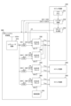
- 2 is a block diagram showing a configuration example of a logic circuit and a body bias control unit according to the first embodiment of the present technology
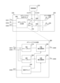
- FIG. 2 is a block diagram showing a configuration example of a body-bias generation block according to the first embodiment of the present technology
- FIG. FIG. 11 is a cross-sectional view showing an example of a bulk structure in a comparative example.
- SOI Silicon On Insulator
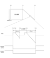
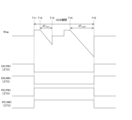
- FIG. 4 is a timing chart showing an example of an operation of the solid-state imaging element according to the first embodiment of the present technology.
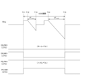
- 10 is a timing chart showing another example of the operation of the solid-state imaging element according to the first embodiment of the present technology.
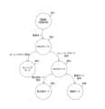
- 4 is an example of a state transition diagram of a solid-state imaging element according to the first embodiment of the present technology;
- FIG. 11 is a diagram illustrating an example of control content for each mode in the first embodiment of the present technology.
- 4 is a flowchart showing an example of an operation of the solid-state imaging element according to the first embodiment of the present technology.
- 11 is a block diagram showing a configuration example of a body-bias generation block according to a modified example of the first embodiment of the present technology;
- FIG. 11 is a timing chart showing an example of an operation of a solid-state imaging element according to a modified example of the first embodiment of the present technology.
- 13 is a timing chart showing another example of the operation of the solid-state imaging element in the modified example of the first embodiment of the present technology.
- FIG. 11 is a block diagram showing a configuration example of a body-bias generation block according to a second embodiment of the present technology; 13 is a graph showing an example of noise characteristics according to the second embodiment of the present technology.
- 13 is a timing chart showing an example of an operation of a solid-state imaging element according to a second embodiment of the present technology.
- 13 is a timing chart showing an example of an operation of a solid-state imaging element according to a modified example of the second embodiment of the present technology.
- 1 is a block diagram showing a schematic configuration example of a vehicle control system;
- FIG. 4 is an explanatory diagram showing an example of an installation position of an imaging unit.
- First embodiment example of controlling a connection switch
- Second embodiment example of controlling the frequency of a clock signal
- First embodiment [Configuration example of imaging device] 1 is a block diagram showing a configuration example of an imaging device 100 according to a first embodiment of the present technology.
- the imaging device 100 is a device for capturing image data, and includes an optical unit 110, a solid-state imaging element 200, and a DSP (Digital Signal Processing) circuit 120.
- the imaging device 100 further includes a display unit 130, an operation unit 140, a bus 150, a frame memory 160, a storage unit 170, and a power supply unit 180.
- the imaging device 100 may be a digital camera or an electronic device having an imaging function (such as a smartphone or a personal computer).
- the imaging device 100 is an example of a semiconductor device described in the claims.
- the optical unit 110 collects light from a subject and guides it to the solid-state imaging element 200.
- the solid-state imaging element 200 generates image data through photoelectric conversion.
- the solid-state imaging element 200 generates image data and supplies it to the DSP circuit 120 via a signal line 209.
- the solid-state imaging element 200 is sometimes called a photodetector.
- the DSP circuit 120 performs a predetermined signal processing on the image data. This DSP circuit 120 outputs the processed image data to the frame memory 160 etc. via the bus 150.
- the display unit 130 displays image data.
- a liquid crystal panel or an organic EL (Electro Luminescence) panel is assumed.
- the operation unit 140 generates an operation signal in accordance with a user's operation.
- the bus 150 is a common path for the optical unit 110, solid-state image sensor 200, DSP circuit 120, display unit 130, operation unit 140, frame memory 160, storage unit 170, and power supply unit 180 to exchange data with each other.
- the frame memory 160 holds image data.
- the storage unit 170 stores various data such as image data.
- the power supply unit 180 supplies power to the solid-state imaging element 200, the DSP circuit 120, the display unit 130, etc.
- Example of the configuration of a solid-state imaging element 2 is a block diagram showing a configuration example of a solid-state imaging element 200 according to the first embodiment of the present technology.
- the solid-state imaging element 200 includes an analog circuit 210, logic circuits 230, 240, and 250, and a body bias control unit 300. These circuits are provided on a single SOI substrate, for example.
- the circuits in the solid-state imaging element 200 may be distributed and arranged on a plurality of semiconductor substrates including an SOI substrate.
- a plurality of pixels 211 are arranged in a two-dimensional lattice. Each pixel 211 photoelectrically converts incident light and generates an analog signal as a pixel signal Ain.
- an ADC 220 is arranged for each column of pixels 211.
- Each ADC 220 includes a comparator 221 and a counter 222.
- the comparator 221 is arranged in the analog circuit 210
- the counter 222 is arranged in the logic circuit 230.
- the comparator 221 compares the pixel signal Ain from the corresponding column with the ramp signal Rmp, and supplies the comparison result to the counter 222.
- the counter 222 counts the count value over a period until the comparison result is inverted, and outputs a digital signal Dout indicating the count value.
- the pixel signal Ain is AD (Analog to Digital) converted by the comparator 221 and counter 222.
- the level of the pixel signal Ain also includes a reset level and a signal level.
- the reset level is the level when the pixel 211 is initialized
- the signal level is the level according to the amount of exposure when the charge is transferred within the pixel 211.
- the counter 222 counts down during the sampling period of the reset level and counts up during the sampling period of the signal level. This allows for AD conversion as well as CDS processing to determine the difference between the reset level and the signal level.
- ADC 220 performs AD conversion and CDS processing, this is not limited to this configuration. It is also possible for the ADC 220 to only perform AD conversion, and for a downstream circuit to perform CDS processing.
- the logic circuits 230, 240, and 250 perform various signal processing on the digital signal Dout.
- the logic circuit 250 outputs image data in which the processed digital signal Dout is arranged to the DSP circuit 120.
- the wells in which the logic circuits 230, 240, and 250 are formed are assumed to be separated.
- the body bias control unit 300 controls the body bias, which is the voltage applied to each well of the logic circuits 230, 240, and 250.
- FIG. 3 is a block diagram showing a configuration example of the logic circuit 230 and the body bias control unit 300 according to the first embodiment of the present technology.
- the body bias control unit 300 includes a regulator circuit 310, power switches 321 to 324, body bias generation blocks 330, 340, 350 and 360, and a control circuit 370.
- the regulator circuit 310 generates a constant output voltage V LDO based on the power supply voltage VDDH.
- the output voltage V LDO is supplied to each of the power switches 321 to 324.
- the power switch 321 opens and closes the path between the output node of the regulator circuit 310 and the body bias generation block 330 in accordance with a control signal SW1 from the logic circuit 230.
- the power switch 322 opens and closes the path between the output node of the regulator circuit 310 and the body bias generation block 340 in accordance with a control signal SW2 from the logic circuit 230.
- the power switch 323 opens and closes the path between the output node of the regulator circuit 310 and the body bias generation block 350 in accordance with a control signal SW3 from the logic circuit 230.
- the power switch 324 opens and closes the path between the output node of the regulator circuit 310 and the body bias generation block 360 in accordance with a control signal SW4 from the logic circuit 230.
- the body bias generation block 330 generates the body biases V PW 1 and V NW 1 for the logic circuit 230 from the output voltage V LDO based on the control signal CNT 1 and the clock signal CK from the logic circuit 230 .
- body-bias generation blocks 340, 350, and 360 The circuit configuration of body-bias generation blocks 340, 350, and 360 is similar to that of body-bias generation block 330.
- the output nodes of body-bias generation blocks 330 and 340 are shorted and commonly connected to logic circuit 230.
- multiple body-bias generation blocks can be connected as shown in the figure to reduce the load on each block.
- the body bias generation block 350 generates body biases V PW3 and V NW3 for the logic circuit 240 from the output voltage V LDO based on the control signal CNT3 and the clock signal CK from the logic circuit 230.
- the body bias generation block 360 generates body biases V PW4 and V NW4 for the logic circuit 250 from the output voltage V LDO based on the control signal CNT4 and the clock signal CK from the logic circuit 230.
- the control circuit 370 controls the output operation of each of the body bias generation blocks 330, 340, 350, and 360 using control signals EN1 to EN4.
- the logic circuit 230 also includes an OTP (One Time Programmable) memory 231, a register circuit 232, and a clock generating unit 233.
- OTP One Time Programmable
- the OTP (One Time Programmable) memory 231 holds the setting values of the control signals SW1 to SW4, the control signals CNT1 to CNT4, and the frequency of the clock signal CK. Note that any memory other than the OTP memory 231 can be used as long as it is non-volatile.
- control signals SW1 to SW4 and the frequency are set appropriately depending on how the imaging device 100 is used.
- control signals CNT1 to CNT4 are signals indicating the body bias values, and are set in advance, for example, by a test circuit (not shown) before the solid-state imaging element 200 starts imaging operation.
- the test circuit for example, generates a test signal in logic circuit 230 or the like, and sets the values of control signals CNT1 to CNT4 for each board based on the results of comparing the value of the test signal with a reference value. These set values can suppress fluctuations in the threshold voltage of transistors caused by process variations.
- the register circuit 232 reads out and stores the setting value from the OTP memory 231.
- the register circuit 232 supplies a control signal for the stored setting value to the body bias control unit 300, and supplies the frequency setting value to the clock generation unit 233.
- the clock generating unit 233 generates a clock signal CK according to the setting value of the register circuit 232 and supplies it to the body bias control unit 300.
- a phase-locked loop circuit or the like is used as the clock generating unit 233.
- the body bias control unit 300 controls only the body bias of the logic circuit, it can also control the body bias of both the analog circuit and the logic circuit.
- the body bias control unit 300 can also control only the body bias of the analog circuit.
- Example of body-bias generation block configuration is a block diagram showing a configuration example of a body bias generation block 330 according to the first embodiment of the present technology.
- the body bias generation block 330 includes a body bias generation unit 400, a P-side connection switch 331, and an N-side connection switch 332.
- the logic circuit 230 includes a predetermined number of pMOS transistors such as a pMOS transistor 234, and a predetermined number of nMOS transistors such as an nMOS transistor 235.
- the body bias generating unit 400 generates body biases V PW1 and V NW1 from the output voltage V LDO based on a clock signal CK and a control signal CNT1.
- the body bias V PW1 is output to a P-side connection switch 331, and the body bias V NW1 is output to an N-side connection switch 332.
- the P-side connection switch 331 opens and closes the path between the body bias generation unit 400 and the well in which the pMOS transistor is formed in accordance with a control signal EN_PW1 from the control circuit 370.
- One end of the P-side connection switch 331 is connected to the body bias generation unit 400, and the other end is connected to the well on the pMOS transistor side via a signal line 408.
- the P-side connection switch 331 is not limited to the nMOS transistor shown in the figure, and any switching element can be applied, such as a pMOS transistor, a shared switching element of an nMOS transistor and a pMOS transistor, a bipolar transistor, or an IGBT (Insulated Gate Bipolar Transistor).
- the N-side connection switch 332 opens and closes the path between the body bias generation unit 400 and the well in which the nMOS transistor is formed in accordance with a control signal EN_NW1 from the control circuit 370.
- One end of the N-side connection switch 332 is connected to the body bias generation unit 400, and the other end is connected to the well on the nMOS transistor side via a signal line 409.
- the N-side connection switch 332 is not limited to the nMOS transistor shown in the figure, and any switching element can be applied, such as a pMOS transistor, a shared switching element of an nMOS transistor and a pMOS transistor, a bipolar transistor, or an IGBT (Insulated Gate Bipolar Transistor).
- control signals EN_PW1 and EN_NW1 in the figure are signals within the aforementioned control signal EN1.
- the body bias generation unit 400 includes a P-side charge pump 410, an N-side charge pump 420, a control block 430, a P-side voltage adjustment unit 440, and an N-side voltage adjustment unit 450.
- the P-side charge pump 410 turns on and off an internal switch (not shown) in synchronization with a clock signal CK to step up or step down (for example, step down) the output voltage V LDO and supplies it to the P-side voltage adjustment unit 440 .
- the N-side charge pump 420 turns on and off an internal switch (not shown) in synchronization with a clock signal CK to step up or step down (for example, step up) the output voltage V LDO and supplies it to the N-side voltage adjustment unit 450 .
- the P-side voltage adjusting unit 440 adjusts the voltage from the P-side charge pump 410 under the control of the control block 430, and outputs the voltage as a body bias V PW1 to the P-side connection switch 331.
- a negative voltage is used as the body bias V PW1 .
- the N-side voltage adjusting section 450 adjusts the voltage from the N-side charge pump 420 under the control of the control block 430, and outputs the voltage as a body bias V NW1 to the N-side connection switch 332.
- a body bias V NW1 for example, a positive voltage is used.
- the control block 430 controls the voltage adjustment amount of each of the P-side voltage adjustment unit 440 and the N-side voltage adjustment unit 450 based on the control signal CNT1 from the register circuit 232.
- the body bias generation unit 400 generates the body biases V PW1 and V NW1 to be applied to the wells.
- the P-side connection switch 331 and the N-side connection switch 332 open and close the path between the body bias generation unit 400 and the wells.
- the control circuit 370 controls these switches.
- control circuit 370 controls both the P-side connection switch 331 and the N-side connection switch 332 to the OFF state during the CDS period in which the CDS processing is performed, and controls both of them to the ON state outside the CDS period. This control makes it possible to prevent noise from being transmitted from the P-side charge pump 410 and the N-side charge pump 420 to the analog circuit 210.
- the body bias is sampled and held by the parasitic capacitance in the SOI substrate.
- the capacitance of the dotted line indicates the parasitic capacitance.
- FIG. 5 is a cross-sectional view showing an example of a bulk structure in a comparative example.
- the semiconductor substrate in the comparative example includes a P substrate 501.
- a deep N well 502 is formed in this P substrate 501.
- N - layer 511 and a P - layer 521 are formed in the deep N - well 502.
- a P + layer 512 and an N + layer source 513 and drain 515 are formed in the N- layer 511.
- An N + layer 522 and a P + layer source 523 and drain 525 are formed in the P-layer 521.
- a body bias of the ground potential VSS is applied to the P + layer 512, and a body bias of the power supply potential VDD is applied to the N + layer 522.
- a gate 514 is formed between the source 513 and the drain 515, which function as an nMOS transistor.
- a gate 524 is formed between the source 523 and the drain 525, which function as a pMOS transistor.
- a bias higher than the ground potential VSS on the nMOS side and lower than the power supply potential VDD on the pMOS side is set as the forward side potential.
- the operating speed improves due to the substrate bias effect, but the diode component in the substrate turns on, increasing the leakage current. For this reason, in the bulk structure, it is practically difficult to control the body bias to the forward side.
- [Configuration Example of SOI Substrate] 6 is a cross-sectional view showing an example of the structure of an SOI substrate 500 according to the first embodiment of the present technology.
- this SOI substrate 500 a circuit in the solid-state imaging element 200 is formed.
- the SOI substrate 500 further includes a predetermined number of insulating layers 503 and insulating films 504 and 505, and differs from the bulk structure of the comparative example in that the positions of the P + layer 512 and the N + layer 522 are different.
- An insulating layer 503 is formed between the P + layers and the N + layers. Furthermore, with the gate side facing up, an insulating film 504 is formed immediately below the channel of the nMOS transistor, and an insulating film 505 is formed immediately below the channel of the pMOS transistor.
- the P + layer 512 is formed in the P- layer 521, and the N + layer 522 is formed in the N- layer 511.
- a body bias VNW1 from the body bias generation block 330 is applied to the N + layer 522.
- This body bias VNW1 is set, for example, in the range of 0 to +2 volts (V).
- a body bias VPW1 from the body bias generation block 330 is applied to the P+ layer 512.
- This body bias VPW1 is set, for example, in the range of 0 to -2 volts (V).
- the N ⁇ layer 511 is an example of an N well as defined in the claims
- the P ⁇ layer 521 is an example of a P well as defined in the claims.
- the SOI structure shown in the figure is called a FD (Fully Depleted)-SOI structure.
- FD-SOI structure the polarity of the layers to which the body bias is applied (i.e., the P + layer 512 and the N + layer 522) is inverted, so that even if the body bias is forward, the diode component in the substrate does not turn on, and leakage current is suppressed.
- the body bias control unit 300 can control the body bias in a direction that lowers the threshold voltage of the transistor, in other words, to the forward side.
- a control signal CNT1 or the like is set for each SOI substrate 500, and the body bias control unit 300 controls the body bias in accordance with the control signal, thereby suppressing fluctuations in threshold voltage due to process variations.
- the body bias on the forward side can reduce the speed variation for each substrate and improve characteristics. It can also lower the difficulty of timing design. Note that for fast-speed SOI substrates, the body bias is not set to the forward side, so the maximum leakage current for the entire product does not change.
- Example of operation of solid-state imaging device 7 is a timing chart showing an example of the operation of the solid-state imaging device 200 according to the first embodiment of the present technology.
- a vertical scanning circuit (not shown) simultaneously exposes all pixels in the analog circuit 210.
- the vertical scanning circuit sequentially selects rows in the analog circuit 210.
- the row selection period includes a CDS period during which AD conversion and CDS processing are performed.
- the CDS period for a certain row is set to be from timing T11 to T15. Over the period from timing T12 to T13 within this CDS period, the ramp signal Rmp gradually drops and sampling of the reset level is performed. This period is set to a sampling period dTsmp1 .
- the ramp signal Rmp gradually drops over the period from timing T14 to T15, and the signal level is sampled. This period is designated as a sampling period dTsmp2 .
- the control circuit 370 sets the control signals EN_PW1 and EN_NW1 to a high level outside the CDS period to control the corresponding connection switches to an on state. For example, the period from the end of the CDS period of one row to the start of the CDS period of the next row and the exposure period correspond to periods outside the CDS period.
- control circuit 370 sets the control signals EN_PW1 and EN_NW1 to a low level during the CDS period, controlling the corresponding connection switches to an off state. During the period when the switches are off, the body bias is sampled and held in the parasitic capacitance in the SOI substrate.
- the body bias generation unit 400 which operates in synchronization with the clock signal CK, becomes a noise source, and the noise may propagate to the analog circuit 210 during readout.
- control circuit 370 controls the P-side connection switch 331 and the N-side connection switch 332 to the off state during the CDS period. This isolates the body bias generation unit 400 from the well, suppressing the propagation of noise to the analog circuit 210 and reducing noise in the pixel signal. As a result, the image quality of the image data is improved.
- the control circuit 370 can turn on and off only one of the switches, such as when improving the speed of only one of the pMOS and nMOS.
- the control circuit 370 turns on one of the P-side connection switch 331 and the N-side connection switch 332 (e.g., the N-side connection switch 332) outside the CDS period, and turns off the other.
- the P-side connection switch 331 and the N-side connection switch 332 are controlled to be in the off state.
- control circuit 370 can turn off the P-side connection switch 331 and the N-side connection switch 332 only during sampling periods Tsmp1 and Tsmp2 in the CDS period, and turn them on outside of these periods.
- FIG. 9 is an example of a state transition diagram of the solid-state imaging element 200 in the first embodiment of the present technology.
- the initial state of the solid-state imaging element 200 is a power-off state 601.
- the solid-state imaging element 200 transitions to a hardware standby state 602.
- the viewing mode is set in the hardware standby state 602
- the solid-state imaging device 200 transitions to a switch standby state 604.
- the viewing mode is a mode for capturing still images or moving images.
- This still image mode 605 is a mode for capturing a still image.
- the solid-state imaging element 200 can transition to sensing mode 603 or video mode 606, for example, in accordance with a user operation.
- This video mode 606 is a mode for capturing video.
- the solid-state imaging element 200 can transition to sensing mode 603 or still image mode 605, for example, in accordance with a user operation.
- the solid-state imaging element 200 transitions, for example, to still image mode 605 or video mode 606.
- FIG. 10 is a diagram showing an example of the control contents for each mode in the first embodiment of the present technology.
- the control circuit 370 In the sensing mode, high image quality is not required compared to the viewing mode. For this reason, the control circuit 370 always controls the P-side connection switch 331 and the N-side connection switch 332 to the off state, and stops the application of the body bias.
- control circuit 370 controls the P-side connection switch 331 and the N-side connection switch 332 to the OFF state during the CDS period. Outside the CDS period, these connection switches are controlled to the ON state.
- FIG. 11 is a flowchart showing an example of the operation of the solid-state imaging device 200 in the first embodiment of the present technology. This operation is started, for example, when a specific application for capturing image data is executed.
- the solid-state imaging element 200 selects one of the rows to be read out (step S901).
- the control circuit 370 turns off the P-side connection switch 331 and the N-side connection switch 332 during the CDS period of the selected row, and the ADC 220 performs AD conversion and CDS processing (step S902).
- the control circuit 370 turns on the P-side connection switch 331 and the N-side connection switch 332 (step S903).
- the solid-state imaging element 200 determines whether or not the readout of all rows has been completed (step S904). If the readout of all rows has not been completed (step S904: No), the solid-state imaging element 200 repeats steps S901 and onward. On the other hand, if the readout of all rows has been completed (step S904: Yes), the solid-state imaging element 200 ends the operation for imaging.
- control circuit 370 turns off the P-side connection switch 331 and the N-side connection switch 332 during the CDS period, thereby reducing noise in the pixel signal.
- the control circuit 370 turns off the P-side connection switch 331 and the N-side connection switch 332 during the CDS period.
- the potentials of the signal lines 408 and 409 between the P-side connection switch 331 and the N-side connection switch 332 and the well may become floating and fluctuate.
- the solid-state imaging device 200 in this modification of the first embodiment differs from the first embodiment in that the signal lines 408 and 409 are set to high impedance during the CDS period.
- FIG. 12 is a block diagram showing an example of the configuration of a body bias generation block 330 in a modified example of the first embodiment of the present technology.
- the body bias generation block 330 in this modified example of the first embodiment differs from the first embodiment in that it further includes a P-side pull-down switch 333 and an N-side pull-down switch 334.
- nMOS transistors are used as these switches.
- the P-side pull-down switch 333 opens and closes the path between the P-side connection switch 331 and the signal line 408 between the well and a predetermined reference potential in accordance with a control signal PD_PW1 from the control circuit 370.
- the ground potential VSS is used as the reference potential.
- the N-side pull-down switch 334 opens and closes the path between the signal line 409 between the N-side connection switch 332 and the well and a predetermined reference potential (such as the ground potential VSS) in accordance with a control signal PD_NW1 from the control circuit 370.
- a predetermined reference potential such as the ground potential VSS
- FIG. 13 is a timing chart showing an example of the operation of the solid-state imaging element 200 in a modified example of the first embodiment of the present technology.
- the method of controlling the control signals EN_PW1 and EN_NW1 is the same as in the first embodiment.
- the control circuit 370 sets the control signals PD_PW1 and PD_NW1 to a high level during the CDS period, thereby controlling the corresponding pull-down switches to an on state. Outside the CDS period, the control circuit 370 sets the control signals PD_PW1 and PD_NW1 to a low level, thereby controlling the corresponding pull-down switches to an off state.
- the control circuit 370 turns on the pull-down switch, thereby fixing the signal lines 408 and 409 to the reference potential. Because these signal lines have high impedance, potential fluctuations during the CDS period can be suppressed.
- control circuit 370 can turn on and off only one of the P-side pull-down switch 333 and the N-side pull-down switch 334.
- control circuit 370 turns on one of the P-side connection switch 331 and the N-side connection switch 332 (for example, the N-side connection switch 332) outside the CDS period, and turns off the other.
- the control circuit 370 turns on one of the P-side connection switch 331 and the N-side connection switch 332 (for example, the N-side connection switch 332) outside the CDS period, and turns off the other.
- both the P-side connection switch 331 and the N-side connection switch 332 are controlled to be in the off state.
- the control circuit 370 turns the N-side pull-down switch 334 off outside the CDS period and turns the P-side pull-down switch 333 on.
- both the P-side pull-down switch 333 and the N-side pull-down switch 334 are controlled to be on.
- the control circuit 370 can also turn the connection switch off only during the sampling period of the CDS period, and turn the connection switch on outside of these periods.
- the pull-down switch is controlled to be on during the sampling period, and the pull-down switch is controlled to be off outside the sampling period.
- control circuit 370 turns on the P-side pull-down switch 333 and the N-side pull-down switch 334 during the CDS period, thereby suppressing the potential fluctuation of the signal line during that period.
- the clock generating unit 233 generates a clock signal CK having a frequency set in the register circuit 232, but there is a risk that an unintended resonant circuit may occur within the circuit of the solid-state imaging element 200, causing an increase in noise at the resonant frequency of the circuit.
- the solid-state imaging element 200 in this second embodiment differs from the first embodiment in that it generates a clock signal CK having a frequency that does not fall within the resonant frequency.
- FIG. 15 is a block diagram showing an example of the configuration of the body bias generation block 330 in the second embodiment of the present technology.
- the control circuit 370 constantly sets the control signals EP_PW1 and EP_NW1 to a high level during imaging. Therefore, the P-side connection switch 331 and the N-side connection switch 332 are controlled to be in the on state even during the CDS period.
- the clock generating unit 233 in the second embodiment generates a clock signal CK having a frequency that does not correspond to the predetermined resonant frequency, and supplies it to the body bias generating unit 400.
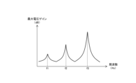
- FIG. 16 is a graph showing an example of noise characteristics in the second embodiment of the present technology.
- the vertical axis in the figure shows the maximum voltage gain of the propagating noise, and the horizontal axis shows the frequency of the clock signal CK.
- the clock generating unit 233 generates a clock signal CK with a frequency that does not fall within these resonant frequencies.
- the test circuit measures noise for each frequency and determines the resonant frequency in advance. Then, the test circuit sets a frequency in the OTP memory 231 that does not correspond to the resonant frequency. Alternatively, the test circuit sets a resonant frequency in the OTP memory 231, and the control circuit 370 controls the clock generation unit 233 to generate a frequency that does not correspond to the resonant frequency. If the resonant frequency is 20 megahertz (MHz), the frequency is controlled to 18 megahertz (MHz) or the like to avoid that frequency.
- FIG. 17 is a timing chart showing an example of the operation of the solid-state imaging device 200 in the second embodiment of the present technology.
- the clock generating unit 233 generates a clock signal CK having a frequency that does not correspond to the resonant frequency.
- the control signals EP_PW1 and EP_NW1 are controlled to a high level even during the CDS period.
- the clock generating unit 233 generates a clock signal CK with a frequency that does not fall within the resonant frequency, thereby reducing noise.
- the clock generating unit 233 generates the clock signal CK having a frequency that does not correspond to the resonant frequency, but the frequency can be lowered within the CDS period.
- the solid-state imaging device 200 in this modified example of the second embodiment differs from the second embodiment in that the frequency of the clock signal CK is lowered within the CDS period.
- FIG. 18 is a timing chart showing an example of the operation of the solid-state imaging device 200 in a modified example of the second embodiment of the present technology.
- the control circuit 370 controls the clock generating unit 233 to generate a clock signal CK with a frequency higher than a predetermined value outside the CDS period, and to generate a clock signal CK with a frequency lower than the predetermined value within the CDS period.
- control circuit 370 controls the frequency of the clock signal CK to 20 megahertz (MHz) outside the CDS period, and reduces the frequency to 2 megahertz (MHz) during the CDS period. This control can reduce noise.
- control circuit 370 can also control the frequency during the sampling period of the CDS period to be lower than the frequency outside the sampling period.
- control circuit 370 reduces the frequency of the clock signal CK within the CDS period, thereby reducing the noise propagating to the analog circuit 210.
- the technology according to the present disclosure can be applied to various products.
- the technology according to the present disclosure may be realized as a device mounted on any type of moving body such as an automobile, an electric vehicle, a hybrid electric vehicle, a motorcycle, a bicycle, a personal mobility device, an airplane, a drone, a ship, or a robot.
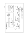
- FIG. 19 is a block diagram showing a schematic configuration example of a vehicle control system, which is an example of a mobile object control system to which the technology disclosed herein can be applied.
- the vehicle control system 12000 includes a plurality of electronic control units connected via a communication network 12001.
- the vehicle control system 12000 includes a drive system control unit 12010, a body system control unit 12020, an outside vehicle information detection unit 12030, an inside vehicle information detection unit 12040, and an integrated control unit 12050.
- Also shown as functional components of the integrated control unit 12050 are a microcomputer 12051, an audio/video output unit 12052, and an in-vehicle network I/F (interface) 12053.
- the drive system control unit 12010 controls the operation of devices related to the drive system of the vehicle according to various programs.
- the drive system control unit 12010 functions as a control device for a drive force generating device for generating the drive force of the vehicle, such as an internal combustion engine or a drive motor, a drive force transmission mechanism for transmitting the drive force to the wheels, a steering mechanism for adjusting the steering angle of the vehicle, and a braking device for generating a braking force for the vehicle.
- the body system control unit 12020 controls the operation of various devices installed in the vehicle body according to various programs.
- the body system control unit 12020 functions as a control device for a keyless entry system, a smart key system, a power window device, or various lamps such as headlamps, tail lamps, brake lamps, turn signals, and fog lamps.
- radio waves or signals from various switches transmitted from a portable device that replaces a key can be input to the body system control unit 12020.
- the body system control unit 12020 accepts the input of these radio waves or signals and controls the vehicle's door lock device, power window device, lamps, etc.
- the outside-vehicle information detection unit 12030 detects information outside the vehicle equipped with the vehicle control system 12000.
- the image capturing unit 12031 is connected to the outside-vehicle information detection unit 12030.
- the outside-vehicle information detection unit 12030 causes the image capturing unit 12031 to capture images outside the vehicle, and receives the captured images.
- the outside-vehicle information detection unit 12030 may perform object detection processing or distance detection processing for people, cars, obstacles, signs, or characters on the road surface, based on the received images.
- the imaging unit 12031 is an optical sensor that receives light and outputs an electrical signal according to the amount of light received.
- the imaging unit 12031 can output the electrical signal as an image, or as distance measurement information.
- the light received by the imaging unit 12031 may be visible light, or may be invisible light such as infrared light.
- the in-vehicle information detection unit 12040 detects information inside the vehicle.
- a driver state detection unit 12041 that detects the state of the driver is connected.
- the driver state detection unit 12041 includes, for example, a camera that captures an image of the driver, and the in-vehicle information detection unit 12040 may calculate the driver's degree of fatigue or concentration based on the detection information input from the driver state detection unit 12041, or may determine whether the driver is dozing off.
- the microcomputer 12051 can calculate control target values for the driving force generating device, steering mechanism, or braking device based on information inside and outside the vehicle acquired by the outside vehicle information detection unit 12030 or the inside vehicle information detection unit 12040, and output control commands to the drive system control unit 12010.
- the microcomputer 12051 can perform cooperative control aimed at realizing the functions of an Advanced Driver Assistance System (ADAS), including vehicle collision avoidance or impact mitigation, following driving based on the distance between vehicles, maintaining vehicle speed, vehicle collision warning, or vehicle lane departure warning.
- ADAS Advanced Driver Assistance System
- the microcomputer 12051 can also perform cooperative control for the purpose of autonomous driving, which allows the vehicle to travel autonomously without relying on the driver's operation, by controlling the driving force generating device, steering mechanism, braking device, etc. based on information about the surroundings of the vehicle acquired by the outside vehicle information detection unit 12030 or the inside vehicle information detection unit 12040.
- the microcomputer 12051 can also output control commands to the body system control unit 12020 based on information outside the vehicle acquired by the outside-vehicle information detection unit 12030. For example, the microcomputer 12051 can control the headlamps according to the position of a preceding vehicle or an oncoming vehicle detected by the outside-vehicle information detection unit 12030, and perform cooperative control aimed at preventing glare, such as switching from high beams to low beams.
- the audio/image output unit 12052 transmits at least one output signal of audio and image to an output device capable of visually or audibly notifying the occupants of the vehicle or the outside of the vehicle of information.
- an audio speaker 12061, a display unit 12062, and an instrument panel 12063 are exemplified as output devices.
- the display unit 12062 may include, for example, at least one of an on-board display and a head-up display.
- FIG. 20 shows an example of the installation position of the imaging unit 12031.
- the imaging unit 12031 includes imaging units 12101, 12102, 12103, 12104, and 12105.
- the imaging units 12101, 12102, 12103, 12104, and 12105 are provided, for example, at the front nose, side mirrors, rear bumper, back door, and upper part of the windshield inside the vehicle cabin of the vehicle 12100.
- the imaging unit 12101 provided at the front nose and the imaging unit 12105 provided at the upper part of the windshield inside the vehicle cabin mainly acquire images of the front of the vehicle 12100.
- the imaging units 12102 and 12103 provided at the side mirrors mainly acquire images of the sides of the vehicle 12100.
- the imaging unit 12104 provided at the rear bumper or back door mainly acquires images of the rear of the vehicle 12100.
- the imaging unit 12105 provided at the upper part of the windshield inside the vehicle cabin is mainly used to detect leading vehicles, pedestrians, obstacles, traffic lights, traffic signs, lanes, etc.
- FIG. 20 shows an example of the imaging ranges of the imaging units 12101 to 12104.
- Imaging range 12111 indicates the imaging range of the imaging unit 12101 provided on the front nose
- imaging ranges 12112 and 12113 indicate the imaging ranges of the imaging units 12102 and 12103 provided on the side mirrors, respectively
- imaging range 12114 indicates the imaging range of the imaging unit 12104 provided on the rear bumper or back door.
- an overhead image of the vehicle 12100 viewed from above is obtained by superimposing the image data captured by the imaging units 12101 to 12104.
- At least one of the imaging units 12101 to 12104 may have a function of acquiring distance information.
- at least one of the imaging units 12101 to 12104 may be a stereo camera consisting of multiple imaging elements, or an imaging element having pixels for phase difference detection.
- the microcomputer 12051 can obtain the distance to each solid object within the imaging ranges 12111 to 12114 and the change in this distance over time (relative speed with respect to the vehicle 12100) based on the distance information obtained from the imaging units 12101 to 12104, and can extract as a preceding vehicle, in particular, the closest solid object on the path of the vehicle 12100 that is traveling in approximately the same direction as the vehicle 12100 at a predetermined speed (e.g., 0 km/h or faster). Furthermore, the microcomputer 12051 can set the inter-vehicle distance that should be maintained in advance in front of the preceding vehicle, and perform automatic braking control (including follow-up stop control) and automatic acceleration control (including follow-up start control). In this way, cooperative control can be performed for the purpose of automatic driving, which runs autonomously without relying on the driver's operation.
- automatic braking control including follow-up stop control
- automatic acceleration control including follow-up start control
- the microcomputer 12051 classifies and extracts three-dimensional object data on three-dimensional objects, such as two-wheeled vehicles, ordinary vehicles, large vehicles, pedestrians, utility poles, and other three-dimensional objects, based on the distance information obtained from the imaging units 12101 to 12104, and can use the data to automatically avoid obstacles.
- the microcomputer 12051 distinguishes obstacles around the vehicle 12100 into obstacles that are visible to the driver of the vehicle 12100 and obstacles that are difficult to see.
- the microcomputer 12051 determines the collision risk, which indicates the risk of collision with each obstacle, and when the collision risk is equal to or exceeds a set value and there is a possibility of a collision, it can provide driving assistance for collision avoidance by outputting an alarm to the driver via the audio speaker 12061 or the display unit 12062, or by forcibly decelerating or steering to avoid a collision via the drive system control unit 12010.
- At least one of the imaging units 12101 to 12104 may be an infrared camera that detects infrared rays.
- the microcomputer 12051 can recognize a pedestrian by determining whether or not a pedestrian is present in the captured image of the imaging units 12101 to 12104. The recognition of such a pedestrian is performed, for example, by a procedure of extracting feature points in the captured image of the imaging units 12101 to 12104 as infrared cameras, and a procedure of performing pattern matching processing on a series of feature points that indicate the contour of an object to determine whether or not it is a pedestrian.
- the audio/image output unit 12052 controls the display unit 12062 to superimpose a rectangular contour line for emphasis on the recognized pedestrian.
- the audio/image output unit 12052 may also control the display unit 12062 to display an icon or the like indicating a pedestrian at a desired position.
- the technology according to the present disclosure can be applied to the imaging unit 12031, etc., among the configurations described above.
- the imaging device 100 in FIG. 1 can be applied to the imaging unit 12031.
- the present technology can also be configured as follows. (1) a transistor formed in a predetermined well in an SOI (Silicon On Insulator) substrate; a body bias generating circuit for generating a body bias to be applied to the well; a connection switch that opens and closes a path between the well and the body bias generation circuit; and a control circuit that controls the connection switch. (2) The semiconductor device according to (1), wherein the control circuit controls the connection switch to an off state during a CDS period in which a CDS (Correlated Double Sampling) process is performed on an analog signal, and controls the connection switch to an on state outside the CDS period.
- a CDS Correlated Double Sampling
- the level of the analog signal includes a reset level and a signal level; the CDS period includes a sampling period of the reset level and a sampling period of the signal level, The semiconductor device according to (1), wherein the control circuit controls the connection switch to an OFF state during the sampling period of the CDS period, and controls the connection switch to an ON state outside the sampling period.
- the transistor includes an nMOS transistor formed in an N well and a pMOS transistor formed in a P well;
- the semiconductor device further comprising a pull-down switch that opens and closes a path between the connection switch and the well and a predetermined reference potential.
- the transistor includes an nMOS transistor formed in an N well and a pMOS transistor formed in a P well;
- the connection switch includes an N-side connection switch that opens and closes a path between the N-well and the body bias generation circuit, and a P-side connection switch that opens and closes a path between the P-well and the body bias generation circuit,
- the pull-down switch is an N-side pull-down switch that opens and closes a path between the N-side connection switch and the N-well and the reference potential;
- the semiconductor device according to (5) above, further comprising a P-side pull-down switch that opens and closes a path between the P-side connection switch and the P-well and a path between the reference potential and the P-well.
- the semiconductor device according to (1) above further comprising a clock generating section which generates a predetermined clock signal and supplies it to the body bias generating section.
- the clock generating unit generates the clock signal having a frequency that does not fall under a predetermined shared frequency.
- the control circuit controls the clock generating unit to generate the clock signal having a frequency higher than a predetermined value within a CDS period in which CDS processing is performed on an analog signal, and to generate the clock signal having a frequency lower than the predetermined value outside the CDS period.
- a body bias generation procedure for generating a body bias to be applied to a well in which a transistor is formed in an SOI (Silicon On Insulator) substrate; and a control procedure for controlling a connection switch that opens and closes a path between the well and the body bias generation circuit.
- SOI Silicon On Insulator
- Imaging device 110
- Optical section 120
- DSP circuit 130 Display section 140
- Operation section 150
- Bus 160
- Power supply section 180
- Solid-state imaging element 210
- Pixel 220 ADC 221 comparator 222 counter 230, 240, 250 logic circuit 231
- OTP memory 232
- register circuit 233
- clock generation unit 234
- pMOS transistor 235 nMOS transistor
- body bias control unit 310 regulator circuit 321 to 324 power switch 330, 340, 350, 360
- body bias generation block 331
- body bias generation unit 410
- P-side charge pump 420
- control block 440
- P-side voltage adjustment unit 450
- N-side voltage adjustment unit 500 SOI substrate 501
Landscapes
- Engineering & Computer Science (AREA)
- Multimedia (AREA)
- Signal Processing (AREA)
- Transforming Light Signals Into Electric Signals (AREA)
- Solid State Image Pick-Up Elements (AREA)
- Metal-Oxide And Bipolar Metal-Oxide Semiconductor Integrated Circuits (AREA)
Abstract
トランジスタが形成されたSOI(Silicon On Insulator)基板において、ノイズを低減する。 半導体装置は、トランジスタと、ボディバイアス生成回路と、接続スイッチと、制御回路とを具備する。トランジスタは、SOI基板内の所定のウェルに形成される。ボディバイアス生成回路は、ウェルに印加するボディバイアスを生成する。接続スイッチは、ウェルとボディバイアス生成回路との間の経路を開閉する。制御回路は、スイッチを制御する。
Description
本技術は、半導体装置に関する。詳しくは、トランジスタのチャネル下に絶縁膜が形成された半導体装置、および、半導体装置の制御方法に関する。
従来より、CIS(CMOS Image Sensors)などの様々な素子や装置において、MOS(Metal-Oxide-Semiconductor)トランジスタが用いられている。例えば、SOI(Silicon On Insulator)構造の基板にMOS型の増幅トランジスタを形成し、そのトランジスタのウェルと、ソースとを接続した撮像装置が提案されている(例えば、特許文献1参照。)。
上述の従来技術では、増幅トランジスタのウェルとソースとを接続することにより、増幅トランジスタの出力電圧のゲインの向上を図っている。しかしながら、上述の撮像装置では、クロック信号に同期して動作する回路から、アナログ回路へノイズが伝搬することがあり、そのノイズを低減することが困難である。
本技術はこのような状況に鑑みて生み出されたものであり、SOI基板を含む半導体装置において、ノイズを低減することを目的とする。
本技術は、上述の問題点を解消するためになされたものであり、その第1の側面は、SOI(Silicon On Insulator)基板内の所定のウェルに形成されたトランジスタと、上記ウェルに印加するボディバイアスを生成するボディバイアス生成回路と、上記ウェルと上記ボディバイアス生成回路との間の経路を開閉する接続スイッチと、上記接続スイッチを制御する制御回路とを具備する半導体装置、および、その制御方法である。これにより、ノイズが低減されるという作用をもたらす。
また、この第1の側面において、上記制御回路は、アナログ信号に対するCDS(Correlated Double Sampling)処理が実行されるCDS期間内に上記接続スイッチをオフ状態に制御し、上記CDS期間外に上記接続スイッチをオン状態に制御してもよい。これにより、CDS期間内のノイズの伝搬が抑制されるという作用をもたらす。
また、この第1の側面において、上記アナログ信号のレベルは、リセットレベルおよび信号レベルを含み、上記CDS期間は、上記リセットレベルのサンプリング期間と上記信号レベルのサンプリング期間とを含み、上記制御回路は、上記CDS期間のうち上記サンプリング期間内に上記接続スイッチをオフ状態に制御し、上記サンプリング期間外に上記接続スイッチをオン状態に制御してもよい。これにより、サンプリング期間内のノイズの伝搬が抑制されるという作用をもたらす。
また、この第1の側面において、上記トランジスタは、Nウェルに形成されたnMOSトランジスタとPウェルに形成されたpMOSトランジスタとを含み、上記接続スイッチは、上記Nウェルおよび上記ボディバイアス生成回路の間の経路を開閉するN側接続スイッチと上記Pウェルおよび上記ボディバイアス生成回路の間の経路を開閉するP側接続スイッチとを含むものであってもよい。これにより、pMOSトランジスタ、nMOSトランジスタのボディバイアスが個別に制御されるという作用をもたらす。
また、この第1の側面において、上記接続スイッチおよび上記ウェルの間の経路と所定の基準電位との間の経路を開閉するプルダウンスイッチをさらに具備してもよい。これにより、電位変動が抑制されるという作用をもたらす。
また、この第1の側面において、上記トランジスタは、Nウェルに形成されたnMOSトランジスタとPウェルに形成されたpMOSトランジスタとを含み、上記接続スイッチは、上記Nウェルおよび上記ボディバイアス生成回路の間の経路を開閉するN側接続スイッチと上記Pウェルおよび上記ボディバイアス生成回路の間の経路を開閉するP側接続スイッチとを含み、上記プルダウンスイッチは、上記N側接続スイッチおよび上記Nウェルの間の経路と上記基準電位との間の経路を開閉するN側プルダウンスイッチと、上記P側接続スイッチおよび上記Pウェルの間の経路と上記基準電位との間の経路を開閉するP側プルダウンスイッチとを含むものであってもよい。これにより、pMOSトランジスタ、nMOSトランジスタのボディバイアスが個別に制御され、電位変動が抑制されるという作用をもたらす。
また、この第1の側面において、所定のクロック信号を生成して上記ボディバイアス生成部に供給するクロック生成部をさらに具備してもよい。これにより、クロック信号に同期してボディバイアスが生成されるという作用をもたらす。
また、この第1の側面において、上記クロック生成部は、所定の共有周波数に該当しない周波数の上記クロック信号を生成してもよい。これにより、ノイズが低減するという作用をもたらす。
また、この第1の側面において、上記制御回路は、上記クロック生成部を制御してアナログ信号に対するCDS処理が実行されるCDS期間内に周波数が所定値より高い上記クロック信号を生成させ、上記CDS期間外に周波数が上記所定値より低い上記クロック信号を生成させてもよい。これにより、CDS期間内のノイズの伝搬が抑制されるという作用をもたらす。
以下、本技術を実施するための形態(以下、実施の形態と称する)について説明する。説明は以下の順序により行う。
1.第1の実施の形態(接続スイッチを制御する例)
2.第2の実施の形態(クロック信号の周波数を制御する例)
3.移動体への応用例
1.第1の実施の形態(接続スイッチを制御する例)
2.第2の実施の形態(クロック信号の周波数を制御する例)
3.移動体への応用例
<1.第1の実施の形態>
[撮像装置の構成例]
図1は、本技術の第1の実施の形態における撮像装置100の一構成例を示すブロック図である。この撮像装置100は、画像データを撮像するための装置であり、光学部110、固体撮像素子200およびDSP(Digital Signal Processing)回路120を備える。さらに撮像装置100は、表示部130、操作部140、バス150、フレームメモリ160、記憶部170および電源部180を備える。撮像装置100としては、デジタルカメラや、撮像機能を持つ電子装置(スマートフォンやパーソナルコンピュータなど)が想定される。なお、撮像装置100は、特許請求の範囲に記載の半導体装置の一例である。
[撮像装置の構成例]
図1は、本技術の第1の実施の形態における撮像装置100の一構成例を示すブロック図である。この撮像装置100は、画像データを撮像するための装置であり、光学部110、固体撮像素子200およびDSP(Digital Signal Processing)回路120を備える。さらに撮像装置100は、表示部130、操作部140、バス150、フレームメモリ160、記憶部170および電源部180を備える。撮像装置100としては、デジタルカメラや、撮像機能を持つ電子装置(スマートフォンやパーソナルコンピュータなど)が想定される。なお、撮像装置100は、特許請求の範囲に記載の半導体装置の一例である。
光学部110は、被写体からの光を集光して固体撮像素子200に導くものである。固体撮像素子200は、光電変換により画像データを生成するものである。この固体撮像素子200は、画像データを生成し、DSP回路120に信号線209を介して供給する。固体撮像素子200は、光検出装置と称することもある。
DSP回路120は、画像データに対して所定の信号処理を実行するものである。このDSP回路120は、処理後の画像データを、バス150を介してフレームメモリ160などに出力する。
表示部130は、画像データを表示するものである。表示部130としては、例えば、液晶パネルや有機EL(Electro Luminescence)パネルが想定される。操作部140は、ユーザの操作に従って操作信号を生成するものである。
バス150は、光学部110、固体撮像素子200、DSP回路120、表示部130、操作部140、フレームメモリ160、記憶部170および電源部180が互いにデータをやりとりするための共通の経路である。
フレームメモリ160は、画像データを保持するものである。記憶部170は、画像データなどの様々なデータを記憶するものである。電源部180は、固体撮像素子200、DSP回路120や表示部130などに電源を供給するものである。
[固体撮像素子の構成例]
図2は、本技術の第1の実施の形態における固体撮像素子200の一構成例を示すブロック図である。この固体撮像素子200は、アナログ回路210と、ロジック回路230、240および250と、ボディバイアス制御部300とを備える。これらの回路は、例えば、単一のSOI基板に設けられる。なお、固体撮像素子200内の回路を、SOI基板を含む複数の半導体基板に分散して配置することもできる。
図2は、本技術の第1の実施の形態における固体撮像素子200の一構成例を示すブロック図である。この固体撮像素子200は、アナログ回路210と、ロジック回路230、240および250と、ボディバイアス制御部300とを備える。これらの回路は、例えば、単一のSOI基板に設けられる。なお、固体撮像素子200内の回路を、SOI基板を含む複数の半導体基板に分散して配置することもできる。
アナログ回路210には、複数の画素211が二次元格子状に配列される。画素211のそれぞれは、入射光を光電変換してアナログ信号を画素信号Ainとして生成するものである。
また、画素211の列ごとにADC220が配列される。ADC220のそれぞれは、コンパレータ221およびカウンタ222を備える。例えば、コンパレータ221は、アナログ回路210内に配置され、カウンタ222がロジック回路230内に配置される。
コンパレータ221は、対応する列からの画素信号Ainと、ランプ信号Rmpとを比較し、比較結果をカウンタ222に供給するものである。カウンタ222は、比較結果が反転するまでの期間に亘って計数値を計数し、その計数値を示すデジタル信号Doutを出力するものである。これらのコンパレータ221およびカウンタ222により、画素信号AinがAD(Analog to Digital)変換される。
また、画素信号Ainのレベルは、リセットレベルおよび信号レベルを含む。ここで、リセットレベルは、画素211が初期化されたときのレベルであり、信号レベルは、画素211内で電荷が転送されたときの、露光量に応じたレベルである。
そして、カウンタ222は、リセットレベルのサンプリング期間内にダウンカウントし、信号レベルのサンプリング期間内にアップカウントする。これにより、AD変換とともに、リセットレベルと信号レベルとの差分を求めるCDS処理が行われる。
なお、ADC220は、AD変換およびCDS処理を行っているが、この構成に限定されない。ADC220がAD変換のみを行い、後段の回路がCDS処理を実行することもできる。
ロジック回路230、240および250は、デジタル信号Doutに対し、各種の信号処理を行うものである。ロジック回路250は、処理後のデジタル信号Doutを配列した画像データをDSP回路120に出力する。SOI基板において、ロジック回路230、240および250のそれぞれが形成されたウェルは分離されているものとする。
ボディバイアス制御部300は、ロジック回路230、240および250のそれぞれのウェルに印加する電圧であるボディバイアスを制御するものである。
[ロジック回路およびボディバイアス制御部の構成例]
図3は、本技術の第1の実施の形態におけるロジック回路230およびボディバイアス制御部300の一構成例を示すブロック図である。
図3は、本技術の第1の実施の形態におけるロジック回路230およびボディバイアス制御部300の一構成例を示すブロック図である。
ボディバイアス制御部300は、レギュレータ回路310と、電源スイッチ321から324と、ボディバイアス生成ブロック330、340、350および360と、制御回路370とを備える。
レギュレータ回路310は、電源電圧VDDHに基づいて、一定の出力電圧VLDOを生成するものである。出力電圧VLDOは、電源スイッチ321から324のそれぞれに供給される。
電源スイッチ321は、ロジック回路230からの制御信号SW1に従ってレギュレータ回路310の出力ノードとボディバイアス生成ブロック330との間の経路を開閉するものである。
電源スイッチ322は、ロジック回路230からの制御信号SW2に従ってレギュレータ回路310の出力ノードとボディバイアス生成ブロック340との間の経路を開閉するものである。
電源スイッチ323は、ロジック回路230からの制御信号SW3に従ってレギュレータ回路310の出力ノードとボディバイアス生成ブロック350との間の経路を開閉するものである。
電源スイッチ324は、ロジック回路230からの制御信号SW4に従ってレギュレータ回路310の出力ノードとボディバイアス生成ブロック360との間の経路を開閉するものである。
ボディバイアス生成ブロック330は、ロジック回路230からの制御信号CNT1およびクロック信号CKに基づいて、ロジック回路230へのボディバイアスVPW1およびVNW1を出力電圧VLDOから生成するものである。
ボディバイアス生成ブロック340、350および360の回路構成は、ボディバイアス生成ブロック330と同様である。ボディバイアス生成ブロック330および340の出力ノードはショートされ、ロジック回路230に共通に接続される。ロジック回路の回路規模が大きい場合、同図に例示するように複数のボディバイアス生成ブロックを接続し、個々のブロックの負荷を軽減することができる。
ボディバイアス生成ブロック350は、ロジック回路230からの制御信号CNT3およびクロック信号CKに基づいて、ロジック回路240へのボディバイアスVPW3およびVNW3を出力電圧VLDOから生成する。ボディバイアス生成ブロック360は、ロジック回路230からの制御信号CNT4およびクロック信号CKに基づいて、ロジック回路250へのボディバイアスVPW4およびVNW4を出力電圧VLDOから生成する。
制御回路370は、制御信号EN1からEN4により、ボディバイアス生成ブロック330、340、350および360のそれぞれの出力動作を制御するものである。
また、ロジック回路230内には、OTP(One Time Programmable)メモリ231、レジスタ回路232およびクロック生成部233を備える。
OTP(One Time Programmable)メモリ231は、制御信号SW1からSW4と、制御信号CNT1からCNT4と、クロック信号CKの周波数とのそれぞれの設定値を保持するものである。なお、不揮発性のものであれば、OTPメモリ231以外のメモリを用いることもできる。
制御信号SW1からSW4と、周波数とのそれぞれの設定値は、撮像装置100の利用方法に応じて適宜に設定される。また、制御信号CNT1からCNT4は、ボディバイアスの値を示す信号であり、例えば、固体撮像素子200の撮像動作開始前に、テスト回路(不図示)により予め設定される。
テスト回路は、例えば、ロジック回路230などにテスト信号を生成させ、そのテスト信号の値と基準値との比較結果に基づいて制御信号CNT1からCNT4のそれぞれの値を基板ごとに設定する。これらの設定値により、プロセスばらつきに起因する、トランジスタの閾値電圧の変動を抑制することができる。
レジスタ回路232は、OTPメモリ231から設定値を読み出して保持するものである。このレジスタ回路232は、保持した設定値の制御信号をボディバイアス制御部300に供給し、周波数の設定値をクロック生成部233に供給する。
クロック生成部233は、レジスタ回路232の設定値に従ってクロック信号CKを生成し、ボディバイアス制御部300に供給するものである。位相同期回路などがクロック生成部233として用いられる。
なお、ボディバイアス制御部300は、ロジック回路のボディバイアスのみを制御しているが、アナログ回路およびロジック回路の両方のボディバイアスを制御することもできる。また、ボディバイアス制御部300は、アナログ回路のボディバイアスのみを制御することもできる。
[ボディバイアス生成ブロックの構成例]
図4は、本技術の第1の実施の形態におけるボディバイアス生成ブロック330の一構成例を示すブロック図である。このボディバイアス生成ブロック330は、ボディバイアス生成部400、P側接続スイッチ331、および、N側接続スイッチ332を備える。ロジック回路230は、pMOSトランジスタ234などの所定数のpMOSトランジスタと、nMOSトランジスタ235などの所定数のnMOSトランジスタとを含む。
図4は、本技術の第1の実施の形態におけるボディバイアス生成ブロック330の一構成例を示すブロック図である。このボディバイアス生成ブロック330は、ボディバイアス生成部400、P側接続スイッチ331、および、N側接続スイッチ332を備える。ロジック回路230は、pMOSトランジスタ234などの所定数のpMOSトランジスタと、nMOSトランジスタ235などの所定数のnMOSトランジスタとを含む。
ボディバイアス生成部400は、クロック信号CKおよび制御信号CNT1に基づいて、ボディバイアスVPW1およびVNW1を出力電圧VLDOから生成するものである。ボディバイアスVPW1はP側接続スイッチ331へ出力され、ボディバイアスVNW1はN側接続スイッチ332へ出力される。
P側接続スイッチ331は、制御回路370からの制御信号EN_PW1に従って、ボディバイアス生成部400とpMOSトランジスタが形成されたウェルとの間の経路を開閉するものである。P側接続スイッチ331の一端は、ボディバイアス生成部400に接続され、他端は、信号線408を介してpMOSトランジスタ側のウェルに接続される。尚、P側接続スイッチ331は、図示されているnMOSトランジスタに限定されず、pMOSトランジスタ、nMOSトランジスタとpMOSトランジスタの共有スイッチング素子、バイポーラトランジスタやIGBT(Insulated Gate Bipolar Transistor)等の任意のスイッチング素子を適用することが可能である。
N側接続スイッチ332は、制御回路370からの制御信号EN_NW1に従って、ボディバイアス生成部400とnMOSトランジスタが形成されたウェルとの間の経路を開閉するものである。N側接続スイッチ332の一端は、ボディバイアス生成部400に接続され、他端は、信号線409を介してnMOSトランジスタ側のウェルに接続される。尚、N側接続スイッチ332は、図示されているnMOSトランジスタに限定されず、pMOSトランジスタ、nMOSトランジスタとpMOSトランジスタの共有スイッチング素子、バイポーラトランジスタやIGBT(Insulated Gate Bipolar Transistor)等の任意のスイッチング素子を適用することが可能である。
同図の制御信号EN_PW1およびEN_NW1は、前述の制御信号EN1内の信号である。
ボディバイアス生成部400は、P側チャージポンプ410、N側チャージポンプ420、制御ブロック430、P側電圧調整部440およびN側電圧調整部450を備える。
P側チャージポンプ410は、クロック信号CKに同期して内部のスイッチ(不図示)をオンオフして出力電圧VLDOを昇圧または降圧(例えば、降圧)し、P側電圧調整部440に供給するものである。
N側チャージポンプ420は、クロック信号CKに同期して内部のスイッチ(不図示)をオンオフして出力電圧VLDOを昇圧または降圧(例えば、昇圧)し、N側電圧調整部450に供給するものである。
P側電圧調整部440は、P側チャージポンプ410からの電圧を制御ブロック430の制御に従って調整し、ボディバイアスVPW1としてP側接続スイッチ331へ出力するものである。ボディバイアスVPW1として、例えば、負電圧が用いられる。
N側電圧調整部450は、N側チャージポンプ420からの電圧を制御ブロック430の制御に従って調整し、ボディバイアスVNW1としてN側接続スイッチ332へ出力するものである。ボディバイアスVNW1として、例えば、正電圧が用いられる。
制御ブロック430は、レジスタ回路232からの制御信号CNT1に基づいて、P側電圧調整部440およびN側電圧調整部450のそれぞれの電圧の調整量を制御するものである。
上述した構成により、ボディバイアス生成部400は、ウェルに印加するボディバイアスVPW1およびVNW1を生成する。P側接続スイッチ331およびN側接続スイッチ332は、ボディバイアス生成部400とウェルとの間の経路を開閉する。制御回路370は、それらのスイッチを制御する。
例えば、制御回路370は、CDS処理が実行されるCDS期間内にP側接続スイッチ331およびN側接続スイッチ332の両方をオフ状態に制御し、CDS期間外に、それらの両方をオン状態に制御する。この制御により、P側チャージポンプ410やN側チャージポンプ420から、アナログ回路210へのノイズの伝搬を防止することができる。
P側接続スイッチ331およびN側接続スイッチ332がオフ状態の期間内において、ボディバイアスは、SOI基板内の寄生容量にサンプルホールドされる。同図において、点線の容量は、寄生容量を示す。
ここで、絶縁膜の無い一般的なバルク構造を用いる装置を比較例として想定する。
図5は、比較例におけるバルク構造の一例を示す断面図である。比較例の半導体基板は、P基板501を含む。このP基板501に、ディープNウェル502が形成される。
ディープNウェル502内に、N-層511およびP-層521が形成される。N-層511内に、P+層512と、N+層のソース513およびドレイン515とが形成される。P-層521内に、N+層522と、P+層のソース523およびドレイン525とが形成される。
P+層512に接地電位VSSのボディバイアスが印加され、N+層522に電源電位VDDのボディバイアスが印加される。また、ソース513およびドレイン515の間にはゲート514が形成され、これらは、nMOSトランジスタとして機能する。ソース523およびドレイン525の間にはゲート524が形成され、これらは、pMOSトランジスタとして機能する。nMOS側において接地電位VSSより高く、pMOS側において電源電位VDDより低いバイアスをフォワード側の電位とする。
比較例においてボディバイアスをフォワード側とすれば、基板バイアス効果により動作スピードが向上するが、基板内のダイオード成分がオンしてリーク電流が増大してしまう。このため、バルク構造では、事実上、ボディバイアスをフォワード側に制御することが困難である。
ただし、リーク電流が増大しても動作スピードを向上させたいケースや、一部の回路でのみ、ボディバイアスがフォワード側に制御されるケースはある。具体的には、高速動作が要求される差動対の回路などのアナログ回路が想定される。一方、アナログ回路に比べてロジック回路は単純な論理セル構造であり、トランジスタの閾値電圧を制御する必要が無いため、ロジック回路のボディバイアスがフォワード側に制御されることは殆どない。
[SOI基板の構成例]
図6は、本技術の第1の実施の形態におけるSOI基板500の構造の一例を示す断面図である。このSOI基板500には、固体撮像素子200内の回路が形成される。
図6は、本技術の第1の実施の形態におけるSOI基板500の構造の一例を示す断面図である。このSOI基板500には、固体撮像素子200内の回路が形成される。
SOI基板500は、所定数の絶縁層503と、絶縁膜504および505とをさらに備え、P+層512およびN+層522の位置が異なる点において比較例のバルク構造と異なる。
P+層やN+層の間には、絶縁層503が形成される。また、ゲート側を上側として、nMOSトランジスタのチャネル直下には絶縁膜504が形成され、pMOSトランジスタのチャネル直下には絶縁膜505が形成される。
また、P+層512は、P-層521内に形成され、N+層522は、N-層511内に形成される。N+層522には、ボディバイアス生成ブロック330からのボディバイアスVNW1が印加される。このボディバイアスVNW1は、例えば、0から+2ボルト(V)の範囲で設定される。P+層512には、ボディバイアス生成ブロック330からのボディバイアスVPW1が印加される。このボディバイアスVPW1は、例えば、0から-2ボルト(V)の範囲で設定される。
なお、N-層511は、特許請求の範囲に記載のNウェルの一例であり、P-層521は、特許請求の範囲に記載のPウェルの一例である。
同図に例示したSOI構造は、FD(Fully Depleted)-SOI構造と呼ばれる。このFD-SOI構造では、ボディバイアスを印加する層(すなわち、P+層512およびN+層522)の極性を反転しているため、ボディバイアスがフォワード側であっても、基板内のダイオード成分がオンせず、リーク電流が抑制される。
このため、ボディバイアス制御部300は、トランジスタの閾値電圧が低くなる方向、言い換えれば、フォワード側にボディバイアスを制御することができる。SOI基板500ごとに制御信号CNT1等を設定しておき、ボディバイアス制御部300が、その制御信号に従ってボディバイアスを制御することにより、プロセスばらつきによる閾値電圧の変動を抑制することができる。
例えば、スピードの遅いSOI基板について、フォワード側のボディバイアスを設定することにより、基板ごとのスピードのばらつきを低減し、特性を改善することができる。また、タイミング設計の難易度を下げることができる。なお、スピードの速いSOI基板では、ボディバイアスをフォワード側にしないため、製品全体のリーク電流の最大値は変わらない。
[固体撮像素子の動作例]
図7は、本技術の第1の実施の形態における固体撮像素子200の動作の一例を示すタイミングチャートである。タイミングT0からT1までの露光期間内に、垂直走査回路(不図示)は、アナログ回路210内の全画素を同時に露光させる。タイミングT1からT2までの読出し期間内に、垂直走査回路は、アナログ回路210内の行を順に選択する。
図7は、本技術の第1の実施の形態における固体撮像素子200の動作の一例を示すタイミングチャートである。タイミングT0からT1までの露光期間内に、垂直走査回路(不図示)は、アナログ回路210内の全画素を同時に露光させる。タイミングT1からT2までの読出し期間内に、垂直走査回路は、アナログ回路210内の行を順に選択する。
行の選択期間は、AD変換およびCDS処理が行われるCDS期間を含む。ある行のCDS期間をタイミングT11からT15とする。このCDS期間内のタイミングT12からT13までの期間に亘ってランプ信号Rmpが徐々に降下し、リセットレベルのサンプリングが実行される。この期間をサンプリング期間dTsmp1とする。
そして、タイミングT14からT15までの期間に亘ってランプ信号Rmpが徐々に降下し、信号レベルのサンプリングが実行される。この期間をサンプリング期間dTsmp2とする。
制御回路370は、CDS期間外に制御信号EN_PW1およびEN_NW1をハイレベルにして、対応する接続スイッチをオン状態に制御する。例えば、ある行のCDS期間の終了時から次の行のCDS期間の開始時までの期間や露光期間が、CDS期間外の期間に該当する。
また、制御回路370は、CDS期間内に制御信号EN_PW1およびEN_NW1をローレベルにして、対応する接続スイッチをオフ状態に制御する。スイッチがオフの期間内において、SOI基板内の寄生容量にボディバイアスがサンプルホールドされる。
P側接続スイッチ331およびN側接続スイッチ332が常にオン状態の場合、クロック信号CKに同期して動作するボディバイアス生成部400がノイズ源となり、そのノイズが、読出しの際にアナログ回路210に伝搬するおそれがある。
そこで、制御回路370は、同図に例示するように、CDS期間内に、P側接続スイッチ331およびN側接続スイッチ332をオフ状態に制御する。これにより、ボディバイアス生成部400がウェルから分離されるため、アナログ回路210へのノイズの伝搬を抑制し、画素信号内のノイズを低減することができる。この結果、画像データの画質が向上する。
なお、行を順に選択して露光を開始させるローリングシャッター方式を用いることもできる。この場合は、露光期間の一部とCDS期間とが重複するが、同様に、CDS期間内にスイッチがオフ状態に制御される。
また、図8におけるaに例示するように、制御回路370は、pMOSおよびnMOSの一方のみのスピードを向上させる場合などに、一方のスイッチのみをオンオフすることもできる。この場合、制御回路370は、CDS期間外にP側接続スイッチ331およびN側接続スイッチ332の一方(例えば、N側接続スイッチ332)をオン状態にし、他方をオフ状態にする。CDS期間内は、P側接続スイッチ331およびN側接続スイッチ332の両方がオフ状態に制御される。
また、同図におけるbに例示するように、制御回路370は、CDS期間のうち、サンプリング期間Tsmp1およびTsmp2のみにP側接続スイッチ331およびN側接続スイッチ332をオフ状態にし、それらの期間外にオン状態にすることもできる。
図9は、本技術の第1の実施の形態における固体撮像素子200の状態遷移図の一例である。この固体撮像素子200の初期状態は、電源断状態601であるものとする。その電源断状態601において電源が投入されると、固体撮像素子200は、ハードウェアスタンバイ状態602に遷移する。
ハードウェアスタンバイ状態602においてビューイングモードが設定されると、固体撮像素子200は、スイッチスタンバイ状態604に遷移する。ここで、ビューイングモードは、静止画または動画を撮像するためのモードである。
スイッチスタンバイ状態604において静止画モードが設定されると、固体撮像素子200は、静止画モード605に遷移する。この静止画モード605は、静止画を撮像するためのモードである。
静止画モード605において撮像が終了した場合、固体撮像素子200は、例えば、ユーザの操作に従って、センシングモード603や動画モード606に遷移することができる。
スイッチスタンバイ状態604において動画モードが設定されると、固体撮像素子200は、動画モード606に遷移する。この動画モード606は、動画を撮像するためのモードである。
動画モード606において撮像が終了した場合、固体撮像素子200は、例えば、ユーザの操作に従って、センシングモード603や静止画モード605に遷移することができる。
ハードウェアスタンバイ状態602においてセンシングモードが設定されると、固体撮像素子200は、センシングモード603に遷移する。センシングモード603は、動体を検出するためのモードである。
センシングモード603において動体が検出されると、固体撮像素子200は、例えば、静止画モード605または動画モード606に遷移する。
図10は、本技術の第1の実施の形態におけるモード毎の制御内容の一例を示す図である。センシングモードでは、ビューイングモードと比較して高画質が要求されない。このため、制御回路370は、常にP側接続スイッチ331およびN側接続スイッチ332をオフ状態に制御し、ボディバイアスの印加を停止する。
一方、静止画モードおよび動画モードでは、センシングモードと比較して高画質が要求される。このため、制御回路370は、CDS期間内にP側接続スイッチ331およびN側接続スイッチ332をオフ状態に制御する。CDS期間外では、それらの接続スイッチがオン状態に制御される。
図11は、本技術の第1の実施の形態における固体撮像素子200の動作の一例を示すフローチャートである。この動作は、例えば、画像データを撮像するための所定のアプリケーションが実行されたときに開始される。
固体撮像素子200は、いずれかの行を読出し対象として選択する(ステップS901)。制御回路370は、選択された行のCDS期間内にP側接続スイッチ331およびN側接続スイッチ332をオフ状態にし、ADC220はAD変換およびCDS処理を行う(ステップS902)。CDS処理の終了時に、制御回路370は、P側接続スイッチ331およびN側接続スイッチ332をオン状態にする(ステップS903)。
固体撮像素子200は、全行の読出しが完了したか否かを判断する(ステップS904)。全行の読出しが完了していない場合(ステップS904:No)、固体撮像素子200は、ステップS901以降を繰り返す。一方、全行の読出しが完了した場合(ステップS904:Yes)、固体撮像素子200は、撮像のための動作を終了する。
このように、本技術の第1の実施の形態によれば、制御回路370がCDS期間内にP側接続スイッチ331およびN側接続スイッチ332をオフ状態にするため、画素信号内のノイズを低減することができる。
[変形例]
上述の第1の実施の形態では、制御回路370が、P側接続スイッチ331およびN側接続スイッチ332をCDS期間内にオフ状態にしていた。しかし、CDS期間内に、P側接続スイッチ331およびN側接続スイッチ332とウェルの間の信号線408および409のそれぞれの電位が浮遊状態となり、変動するおそれがある。この第1の実施の形態の変形例における固体撮像素子200は、CDS期間内に信号線408および409をハイインピーダンスにする点において第1の実施の形態と異なる。
上述の第1の実施の形態では、制御回路370が、P側接続スイッチ331およびN側接続スイッチ332をCDS期間内にオフ状態にしていた。しかし、CDS期間内に、P側接続スイッチ331およびN側接続スイッチ332とウェルの間の信号線408および409のそれぞれの電位が浮遊状態となり、変動するおそれがある。この第1の実施の形態の変形例における固体撮像素子200は、CDS期間内に信号線408および409をハイインピーダンスにする点において第1の実施の形態と異なる。
図12は、本技術の第1の実施の形態の変形例におけるボディバイアス生成ブロック330の一構成例を示すブロック図である。この第1の実施の形態の変形例におけるボディバイアス生成ブロック330は、P側プルダウンスイッチ333およびN側プルダウンスイッチ334をさらに備える点において第1の実施の形態と異なる。これらのスイッチとして、例えば、nMOSトランジスタが用いられる。
P側プルダウンスイッチ333は、制御回路370からの制御信号PD_PW1に従って、P側接続スイッチ331およびウェルの間の信号線408と所定の基準電位との間の経路を開閉するものである。基準電位として、例えば、接地電位VSSが用いられる。
N側プルダウンスイッチ334は、制御回路370からの制御信号PD_NW1に従って、N側接続スイッチ332およびウェルの間の信号線409と所定の基準電位(接地電位VSSなど)との間の経路を開閉するものである。
これらのプルダウンスイッチと接続スイッチとは排他的に制御される。
図13は、本技術の第1の実施の形態の変形例における固体撮像素子200の動作の一例を示すタイミングチャートである。第1の実施の形態の変形例において、制御信号EN_PW1およびEN_NW1の制御方法は、第1の実施の形態と同様である。
制御回路370は、CDS期間内に制御信号PD_PW1およびPD_NW1をハイレベルにして、対応するプルダウンスイッチをオン状態に制御する。また、制御回路370は、CDS期間外に、制御信号PD_PW1およびPD_NW1をローレベルにして、対応するプルダウンスイッチをオフ状態に制御する。
同図に例示するように、CDS期間内に制御回路370がプルダウンスイッチをオン状態にすることにより、信号線408および409を基準電位に固定することができる。これらの信号線がハイインピーダンスとなるため、CDS期間内の電位変動を抑制することができる。
なお、図14に例示するように、制御回路370は、P側プルダウンスイッチ333およびN側プルダウンスイッチ334の一方のみをオンオフすることができる。
この場合、制御回路370は、CDS期間外にP側接続スイッチ331およびN側接続スイッチ332の一方(例えば、N側接続スイッチ332)をオン状態にし、他方をオフ状態にする。CDS期間内は、P側接続スイッチ331およびN側接続スイッチ332の両方がオフ状態に制御される。
N側接続スイッチ332のみがオンオフされる場合、制御回路370は、CDS期間外にN側プルダウンスイッチ334をオフ状態にし、P側プルダウンスイッチ333をオン状態にする。CDS期間内は、P側プルダウンスイッチ333およびN側プルダウンスイッチ334の両方がオン状態に制御される。
また、制御回路370は、CDS期間のうち、サンプリング期間のみに接続スイッチをオフ状態にし、それらの期間外に接続スイッチをオン状態にすることもできる。この場合は、サンプリング期間内にプルダウンスイッチがオン状態に制御され、サンプリング期間外にプルダウンスイッチがオフ状態に制御される。
このように、本技術の第1の実施の形態の変形例によれば、制御回路370がCDS期間内にP側プルダウンスイッチ333およびN側プルダウンスイッチ334をオン状態にするため、その期間の信号線の電位変動を抑制することができる。
<2.第2の実施の形態>
上述の第1の実施の形態では、クロック生成部233は、レジスタ回路232に設定された周波数のクロック信号CKを生成していたが、固体撮像素子200の回路内で意図しない共振回路が生じ、その回路の共振周波数でノイズが増大するおそれがある。この第2の実施の形態における固体撮像素子200は、共振周波数に該当しない周波数のクロック信号CKを生成する点において第1の実施の形態と異なる。
上述の第1の実施の形態では、クロック生成部233は、レジスタ回路232に設定された周波数のクロック信号CKを生成していたが、固体撮像素子200の回路内で意図しない共振回路が生じ、その回路の共振周波数でノイズが増大するおそれがある。この第2の実施の形態における固体撮像素子200は、共振周波数に該当しない周波数のクロック信号CKを生成する点において第1の実施の形態と異なる。
図15は、本技術の第2の実施の形態におけるボディバイアス生成ブロック330の一構成例を示すブロック図である。この第2の実施の形態において、制御回路370は、撮像中に制御信号EP_PW1およびEP_NW1を常にハイレベルにする。このため、CDS期間内もP側接続スイッチ331およびN側接続スイッチ332はオン状態に制御される。
また、第2の実施の形態のクロック生成部233は、所定の共振周波数に該当しない周波数のクロック信号CKを生成し、ボディバイアス生成部400に供給する。
図16は、本技術の第2の実施の形態におけるノイズ特性の一例を示すグラフである。同図における縦軸は、伝搬するノイズの最大電圧ゲインを示し、横軸は、クロック信号CKの周波数を示す。
ノイズの伝搬経路に意図しない共振回路が生じる場合、その回路の共振周波数でノイズが増大することがある。同図では、共振周波数f1、f2、f3でゲインがピーク値となる。そこで、クロック生成部233は、それらの共振周波数に該当しない周波数のクロック信号CKを生成する。
例えば、テスト回路が周波数ごとにノイズを測定して、予め共振周波数を求めておく。そして、テスト回路は、OTPメモリ231に、共振周波数に該当しない周波数を設定する。あるいは、テスト回路は、OTPメモリ231に共振周波数を設定しておき、制御回路370がクロック生成部233を制御して、その共振周波数に該当しない周波数を生成させる。共振周波数が20メガヘルツ(MHz)の場合、その周波数を避けて18メガヘルツ(MHz)などに周波数が制御される。
図17は、本技術の第2の実施の形態における固体撮像素子200の動作の一例を示すタイミングチャートである。この第2の実施の形態において、クロック生成部233は、共振周波数に該当しない周波数のクロック信号CKを生成する。また、CDS期間内も制御信号EP_PW1およびEP_NW1はハイレベルに制御される。
このように本技術の第2の実施の形態によれば、クロック生成部233が、共振周波数に該当しない周波数のクロック信号CKを生成するため、ノイズを低減することができる。
[変形例]
上述の第2の実施の形態では、クロック生成部233は共振周波数に該当しない周波数のクロック信号CKを生成していたが、CDS期間内に周波数を低下させることもできる。この第2の実施の形態の変形例における固体撮像素子200は、CDS期間内にクロック信号CKの周波数を低下させる点において第2の実施の形態と異なる。
上述の第2の実施の形態では、クロック生成部233は共振周波数に該当しない周波数のクロック信号CKを生成していたが、CDS期間内に周波数を低下させることもできる。この第2の実施の形態の変形例における固体撮像素子200は、CDS期間内にクロック信号CKの周波数を低下させる点において第2の実施の形態と異なる。
図18は、本技術の第2の実施の形態の変形例における固体撮像素子200の動作の一例を示すタイミングチャートである。この第2の実施の形態の変形例において制御回路370は、クロック生成部233を制御して、CDS期間外に所定値より高い周波数のクロック信号CKを生成させ、CDS期間内に所定値より低い周波数のクロック信号CKを生成させる。
例えば、制御回路370は、CDS期間外にクロック信号CKの周波数を20メガヘルツ(MHz)に制御し、CDS期間内にその周波数を2メガヘルツ(MHz)に低下させる。この制御により、ノイズを低減することができる。
また、CDS期間内も制御信号EP_PW1およびEP_NW1はハイレベルに制御される。
なお、制御回路370は、CDS期間のうちサンプリング期間内に、サンプリング期間外よりも低い周波数に制御することもできる。
このように、本技術の第2の実施の形態の変形例によれば、制御回路370がCDS期間内にクロック信号CKの周波数を低下させるため、アナログ回路210に伝搬するノイズを低減することができる。
<3.移動体への応用例>
本開示に係る技術(本技術)は、様々な製品へ応用することができる。例えば、本開示に係る技術は、自動車、電気自動車、ハイブリッド電気自動車、自動二輪車、自転車、パーソナルモビリティ、飛行機、ドローン、船舶、ロボット等のいずれかの種類の移動体に搭載される装置として実現されてもよい。
本開示に係る技術(本技術)は、様々な製品へ応用することができる。例えば、本開示に係る技術は、自動車、電気自動車、ハイブリッド電気自動車、自動二輪車、自転車、パーソナルモビリティ、飛行機、ドローン、船舶、ロボット等のいずれかの種類の移動体に搭載される装置として実現されてもよい。
図19は、本開示に係る技術が適用され得る移動体制御システムの一例である車両制御システムの概略的な構成例を示すブロック図である。
車両制御システム12000は、通信ネットワーク12001を介して接続された複数の電子制御ユニットを備える。図19に示した例では、車両制御システム12000は、駆動系制御ユニット12010、ボディ系制御ユニット12020、車外情報検出ユニット12030、車内情報検出ユニット12040、及び統合制御ユニット12050を備える。また、統合制御ユニット12050の機能構成として、マイクロコンピュータ12051、音声画像出力部12052、及び車載ネットワークI/F(interface)12053が図示されている。
駆動系制御ユニット12010は、各種プログラムにしたがって車両の駆動系に関連する装置の動作を制御する。例えば、駆動系制御ユニット12010は、内燃機関又は駆動用モータ等の車両の駆動力を発生させるための駆動力発生装置、駆動力を車輪に伝達するための駆動力伝達機構、車両の舵角を調節するステアリング機構、及び、車両の制動力を発生させる制動装置等の制御装置として機能する。
ボディ系制御ユニット12020は、各種プログラムにしたがって車体に装備された各種装置の動作を制御する。例えば、ボディ系制御ユニット12020は、キーレスエントリシステム、スマートキーシステム、パワーウィンドウ装置、あるいは、ヘッドランプ、バックランプ、ブレーキランプ、ウィンカー又はフォグランプ等の各種ランプの制御装置として機能する。この場合、ボディ系制御ユニット12020には、鍵を代替する携帯機から発信される電波又は各種スイッチの信号が入力され得る。ボディ系制御ユニット12020は、これらの電波又は信号の入力を受け付け、車両のドアロック装置、パワーウィンドウ装置、ランプ等を制御する。
車外情報検出ユニット12030は、車両制御システム12000を搭載した車両の外部の情報を検出する。例えば、車外情報検出ユニット12030には、撮像部12031が接続される。車外情報検出ユニット12030は、撮像部12031に車外の画像を撮像させるとともに、撮像された画像を受信する。車外情報検出ユニット12030は、受信した画像に基づいて、人、車、障害物、標識又は路面上の文字等の物体検出処理又は距離検出処理を行ってもよい。
撮像部12031は、光を受光し、その光の受光量に応じた電気信号を出力する光センサである。撮像部12031は、電気信号を画像として出力することもできるし、測距の情報として出力することもできる。また、撮像部12031が受光する光は、可視光であっても良いし、赤外線等の非可視光であっても良い。
車内情報検出ユニット12040は、車内の情報を検出する。車内情報検出ユニット12040には、例えば、運転者の状態を検出する運転者状態検出部12041が接続される。運転者状態検出部12041は、例えば運転者を撮像するカメラを含み、車内情報検出ユニット12040は、運転者状態検出部12041から入力される検出情報に基づいて、運転者の疲労度合い又は集中度合いを算出してもよいし、運転者が居眠りをしていないかを判別してもよい。
マイクロコンピュータ12051は、車外情報検出ユニット12030又は車内情報検出ユニット12040で取得される車内外の情報に基づいて、駆動力発生装置、ステアリング機構又は制動装置の制御目標値を演算し、駆動系制御ユニット12010に対して制御指令を出力することができる。例えば、マイクロコンピュータ12051は、車両の衝突回避あるいは衝撃緩和、車間距離に基づく追従走行、車速維持走行、車両の衝突警告、又は車両のレーン逸脱警告等を含むADAS(Advanced Driver Assistance System)の機能実現を目的とした協調制御を行うことができる。
また、マイクロコンピュータ12051は、車外情報検出ユニット12030又は車内情報検出ユニット12040で取得される車両の周囲の情報に基づいて駆動力発生装置、ステアリング機構又は制動装置等を制御することにより、運転者の操作に拠らずに自律的に走行する自動運転等を目的とした協調制御を行うことができる。
また、マイクロコンピュータ12051は、車外情報検出ユニット12030で取得される車外の情報に基づいて、ボディ系制御ユニット12020に対して制御指令を出力することができる。例えば、マイクロコンピュータ12051は、車外情報検出ユニット12030で検知した先行車又は対向車の位置に応じてヘッドランプを制御し、ハイビームをロービームに切り替える等の防眩を図ることを目的とした協調制御を行うことができる。
音声画像出力部12052は、車両の搭乗者又は車外に対して、視覚的又は聴覚的に情報を通知することが可能な出力装置へ音声及び画像のうちの少なくとも一方の出力信号を送信する。図19の例では、出力装置として、オーディオスピーカ12061、表示部12062及びインストルメントパネル12063が例示されている。表示部12062は、例えば、オンボードディスプレイ及びヘッドアップディスプレイの少なくとも一つを含んでいてもよい。
図20は、撮像部12031の設置位置の例を示す図である。
図20では、撮像部12031として、撮像部12101,12102,12103,12104,12105を有する。
撮像部12101,12102,12103,12104,12105は、例えば、車両12100のフロントノーズ、サイドミラー、リアバンパ、バックドア及び車室内のフロントガラスの上部等の位置に設けられる。フロントノーズに備えられる撮像部12101及び車室内のフロントガラスの上部に備えられる撮像部12105は、主として車両12100の前方の画像を取得する。サイドミラーに備えられる撮像部12102,12103は、主として車両12100の側方の画像を取得する。リアバンパ又はバックドアに備えられる撮像部12104は、主として車両12100の後方の画像を取得する。車室内のフロントガラスの上部に備えられる撮像部12105は、主として先行車両又は、歩行者、障害物、信号機、交通標識又は車線等の検出に用いられる。
なお、図20には、撮像部12101ないし12104の撮影範囲の一例が示されている。撮像範囲12111は、フロントノーズに設けられた撮像部12101の撮像範囲を示し、撮像範囲12112,12113は、それぞれサイドミラーに設けられた撮像部12102,12103の撮像範囲を示し、撮像範囲12114は、リアバンパ又はバックドアに設けられた撮像部12104の撮像範囲を示す。例えば、撮像部12101ないし12104で撮像された画像データが重ね合わせられることにより、車両12100を上方から見た俯瞰画像が得られる。
撮像部12101ないし12104の少なくとも1つは、距離情報を取得する機能を有していてもよい。例えば、撮像部12101ないし12104の少なくとも1つは、複数の撮像素子からなるステレオカメラであってもよいし、位相差検出用の画素を有する撮像素子であってもよい。
例えば、マイクロコンピュータ12051は、撮像部12101ないし12104から得られた距離情報を基に、撮像範囲12111ないし12114内における各立体物までの距離と、この距離の時間的変化(車両12100に対する相対速度)を求めることにより、特に車両12100の進行路上にある最も近い立体物で、車両12100と略同じ方向に所定の速度(例えば、0km/h以上)で走行する立体物を先行車として抽出することができる。さらに、マイクロコンピュータ12051は、先行車の手前に予め確保すべき車間距離を設定し、自動ブレーキ制御(追従停止制御も含む)や自動加速制御(追従発進制御も含む)等を行うことができる。このように運転者の操作に拠らずに自律的に走行する自動運転等を目的とした協調制御を行うことができる。
例えば、マイクロコンピュータ12051は、撮像部12101ないし12104から得られた距離情報を元に、立体物に関する立体物データを、2輪車、普通車両、大型車両、歩行者、電柱等その他の立体物に分類して抽出し、障害物の自動回避に用いることができる。例えば、マイクロコンピュータ12051は、車両12100の周辺の障害物を、車両12100のドライバが視認可能な障害物と視認困難な障害物とに識別する。そして、マイクロコンピュータ12051は、各障害物との衝突の危険度を示す衝突リスクを判断し、衝突リスクが設定値以上で衝突可能性がある状況であるときには、オーディオスピーカ12061や表示部12062を介してドライバに警報を出力することや、駆動系制御ユニット12010を介して強制減速や回避操舵を行うことで、衝突回避のための運転支援を行うことができる。
撮像部12101ないし12104の少なくとも1つは、赤外線を検出する赤外線カメラであってもよい。例えば、マイクロコンピュータ12051は、撮像部12101ないし12104の撮像画像中に歩行者が存在するか否かを判定することで歩行者を認識することができる。かかる歩行者の認識は、例えば赤外線カメラとしての撮像部12101ないし12104の撮像画像における特徴点を抽出する手順と、物体の輪郭を示す一連の特徴点にパターンマッチング処理を行って歩行者か否かを判別する手順によって行われる。マイクロコンピュータ12051が、撮像部12101ないし12104の撮像画像中に歩行者が存在すると判定し、歩行者を認識すると、音声画像出力部12052は、当該認識された歩行者に強調のための方形輪郭線を重畳表示するように、表示部12062を制御する。また、音声画像出力部12052は、歩行者を示すアイコン等を所望の位置に表示するように表示部12062を制御してもよい。
以上、本開示に係る技術が適用され得る車両制御システムの一例について説明した。本開示に係る技術は、以上説明した構成のうち、撮像部12031等)に適用され得る。具体的には、図1の撮像装置100は、撮像部12031に適用することができる。撮像部12031に本開示に係る技術を適用することにより、ノイズが低減して、より見やすい撮影画像を得ることができるため、ドライバの疲労を軽減することが可能になる。
なお、上述の実施の形態は本技術を具現化するための一例を示したものであり、実施の形態における事項と、特許請求の範囲における発明特定事項とはそれぞれ対応関係を有する。同様に、特許請求の範囲における発明特定事項と、これと同一名称を付した本技術の実施の形態における事項とはそれぞれ対応関係を有する。ただし、本技術は実施の形態に限定されるものではなく、その要旨を逸脱しない範囲において実施の形態に種々の変形を施すことにより具現化することができる。
なお、本明細書に記載された効果はあくまで例示であって、限定されるものではなく、また、他の効果があってもよい。
なお、本技術は以下のような構成もとることができる。
(1)SOI(Silicon On Insulator)基板内の所定のウェルに形成されたトランジスタと、
前記ウェルに印加するボディバイアスを生成するボディバイアス生成回路と、
前記ウェルと前記ボディバイアス生成回路との間の経路を開閉する接続スイッチと、
前記接続スイッチを制御する制御回路と
を具備する半導体装置。
(2)前記制御回路は、アナログ信号に対するCDS(Correlated Double Sampling)処理が実行されるCDS期間内に前記接続スイッチをオフ状態に制御し、前記CDS期間外に前記接続スイッチをオン状態に制御する
前記(1)記載の半導体装置。
(3)前記アナログ信号のレベルは、リセットレベルおよび信号レベルを含み、
前記CDS期間は、前記リセットレベルのサンプリング期間と前記信号レベルのサンプリング期間とを含み、
前記制御回路は、前記CDS期間のうち前記サンプリング期間内に前記接続スイッチをオフ状態に制御し、前記サンプリング期間外に前記接続スイッチをオン状態に制御する
前記(1)記載の半導体装置。
(4)前記トランジスタは、Nウェルに形成されたnMOSトランジスタとPウェルに形成されたpMOSトランジスタとを含み、
前記接続スイッチは、前記Nウェルおよび前記ボディバイアス生成回路の間の経路を開閉するN側接続スイッチと前記Pウェルおよび前記ボディバイアス生成回路の間の経路を開閉するP側接続スイッチとを含む
前記(1)から(3)のいずれかに記載の半導体装置。
(5)前記接続スイッチおよび前記ウェルの間の経路と所定の基準電位との間の経路を開閉するプルダウンスイッチをさらに具備する前記(1)から(4)のいずれかに記載の半導体装置。
(6)前記トランジスタは、Nウェルに形成されたnMOSトランジスタとPウェルに形成されたpMOSトランジスタとを含み、
前記接続スイッチは、前記Nウェルおよび前記ボディバイアス生成回路の間の経路を開閉するN側接続スイッチと前記Pウェルおよび前記ボディバイアス生成回路の間の経路を開閉するP側接続スイッチとを含み、
前記プルダウンスイッチは、
前記N側接続スイッチおよび前記Nウェルの間の経路と前記基準電位との間の経路を開閉するN側プルダウンスイッチと、
前記P側接続スイッチおよび前記Pウェルの間の経路と前記基準電位との間の経路を開閉するP側プルダウンスイッチと
を含む前記(5)記載の半導体装置。
(7)所定のクロック信号を生成して前記ボディバイアス生成部に供給するクロック生成部をさらに具備する前記(1)記載の半導体装置。
(8)前記クロック生成部は、所定の共有周波数に該当しない周波数の前記クロック信号を生成する
前記(7)記載の半導体装置。
(9)前記制御回路は、前記クロック生成部を制御してアナログ信号に対するCDS処理が実行されるCDS期間内に周波数が所定値より高い前記クロック信号を生成させ、前記CDS期間外に周波数が前記所定値より低い前記クロック信号を生成させる
前記(7)記載の半導体装置。
(10)SOI(Silicon On Insulator)基板内のトランジスタが形成されたウェルに印加するボディバイアスを生成するボディバイアス生成手順と、
前記ウェルと前記ボディバイアス生成回路との間の経路を開閉する接続スイッチを制御する制御手順と
を具備する半導体装置の制御方法。
(1)SOI(Silicon On Insulator)基板内の所定のウェルに形成されたトランジスタと、
前記ウェルに印加するボディバイアスを生成するボディバイアス生成回路と、
前記ウェルと前記ボディバイアス生成回路との間の経路を開閉する接続スイッチと、
前記接続スイッチを制御する制御回路と
を具備する半導体装置。
(2)前記制御回路は、アナログ信号に対するCDS(Correlated Double Sampling)処理が実行されるCDS期間内に前記接続スイッチをオフ状態に制御し、前記CDS期間外に前記接続スイッチをオン状態に制御する
前記(1)記載の半導体装置。
(3)前記アナログ信号のレベルは、リセットレベルおよび信号レベルを含み、
前記CDS期間は、前記リセットレベルのサンプリング期間と前記信号レベルのサンプリング期間とを含み、
前記制御回路は、前記CDS期間のうち前記サンプリング期間内に前記接続スイッチをオフ状態に制御し、前記サンプリング期間外に前記接続スイッチをオン状態に制御する
前記(1)記載の半導体装置。
(4)前記トランジスタは、Nウェルに形成されたnMOSトランジスタとPウェルに形成されたpMOSトランジスタとを含み、
前記接続スイッチは、前記Nウェルおよび前記ボディバイアス生成回路の間の経路を開閉するN側接続スイッチと前記Pウェルおよび前記ボディバイアス生成回路の間の経路を開閉するP側接続スイッチとを含む
前記(1)から(3)のいずれかに記載の半導体装置。
(5)前記接続スイッチおよび前記ウェルの間の経路と所定の基準電位との間の経路を開閉するプルダウンスイッチをさらに具備する前記(1)から(4)のいずれかに記載の半導体装置。
(6)前記トランジスタは、Nウェルに形成されたnMOSトランジスタとPウェルに形成されたpMOSトランジスタとを含み、
前記接続スイッチは、前記Nウェルおよび前記ボディバイアス生成回路の間の経路を開閉するN側接続スイッチと前記Pウェルおよび前記ボディバイアス生成回路の間の経路を開閉するP側接続スイッチとを含み、
前記プルダウンスイッチは、
前記N側接続スイッチおよび前記Nウェルの間の経路と前記基準電位との間の経路を開閉するN側プルダウンスイッチと、
前記P側接続スイッチおよび前記Pウェルの間の経路と前記基準電位との間の経路を開閉するP側プルダウンスイッチと
を含む前記(5)記載の半導体装置。
(7)所定のクロック信号を生成して前記ボディバイアス生成部に供給するクロック生成部をさらに具備する前記(1)記載の半導体装置。
(8)前記クロック生成部は、所定の共有周波数に該当しない周波数の前記クロック信号を生成する
前記(7)記載の半導体装置。
(9)前記制御回路は、前記クロック生成部を制御してアナログ信号に対するCDS処理が実行されるCDS期間内に周波数が所定値より高い前記クロック信号を生成させ、前記CDS期間外に周波数が前記所定値より低い前記クロック信号を生成させる
前記(7)記載の半導体装置。
(10)SOI(Silicon On Insulator)基板内のトランジスタが形成されたウェルに印加するボディバイアスを生成するボディバイアス生成手順と、
前記ウェルと前記ボディバイアス生成回路との間の経路を開閉する接続スイッチを制御する制御手順と
を具備する半導体装置の制御方法。
100 撮像装置
110 光学部
120 DSP回路
130 表示部
140 操作部
150 バス
160 フレームメモリ
170 記憶部
180 電源部
200 固体撮像素子
210 アナログ回路
211 画素
220 ADC
221 コンパレータ
222 カウンタ
230、240、250 ロジック回路
231 OTPメモリ
232 レジスタ回路
233 クロック生成部
234 pMOSトランジスタ
235 nMOSトランジスタ
300 ボディバイアス制御部
310レギュレータ回路
321~324 電源スイッチ
330、340、350、360 ボディバイアス生成ブロック
331 P側接続スイッチ
332 N側接続スイッチ
333 P側プルダウンスイッチ
334 N側プルダウンスイッチ
370 制御回路
400 ボディバイアス生成部
410 P側チャージポンプ
420 N側チャージポンプ
430 制御ブロック
440 P側電圧調整部
450 N側電圧調整部
500 SOI基板
501 P基板
502 ディープNウェル
503 絶縁層
504、505 絶縁膜
511 N-層
512 P+層
513、523 ソース
514、524 ゲート
515、525 ドレイン
521 P-層
522 N+層
12031 撮像部
110 光学部
120 DSP回路
130 表示部
140 操作部
150 バス
160 フレームメモリ
170 記憶部
180 電源部
200 固体撮像素子
210 アナログ回路
211 画素
220 ADC
221 コンパレータ
222 カウンタ
230、240、250 ロジック回路
231 OTPメモリ
232 レジスタ回路
233 クロック生成部
234 pMOSトランジスタ
235 nMOSトランジスタ
300 ボディバイアス制御部
310レギュレータ回路
321~324 電源スイッチ
330、340、350、360 ボディバイアス生成ブロック
331 P側接続スイッチ
332 N側接続スイッチ
333 P側プルダウンスイッチ
334 N側プルダウンスイッチ
370 制御回路
400 ボディバイアス生成部
410 P側チャージポンプ
420 N側チャージポンプ
430 制御ブロック
440 P側電圧調整部
450 N側電圧調整部
500 SOI基板
501 P基板
502 ディープNウェル
503 絶縁層
504、505 絶縁膜
511 N-層
512 P+層
513、523 ソース
514、524 ゲート
515、525 ドレイン
521 P-層
522 N+層
12031 撮像部
Claims (10)
- SOI(Silicon On Insulator)基板内の所定のウェルに形成されたトランジスタと、
前記ウェルに印加するボディバイアスを生成するボディバイアス生成回路と、
前記ウェルと前記ボディバイアス生成回路との間の経路を開閉する接続スイッチと、
前記接続スイッチを制御する制御回路と
を具備する半導体装置。 - 前記制御回路は、アナログ信号に対するCDS(Correlated Double Sampling)処理が実行されるCDS期間内に前記接続スイッチをオフ状態に制御し、前記CDS期間外に前記接続スイッチをオン状態に制御する
請求項1記載の半導体装置。 - 前記アナログ信号のレベルは、リセットレベルおよび信号レベルを含み、
前記CDS期間は、前記リセットレベルのサンプリング期間と前記信号レベルのサンプリング期間とを含み、
前記制御回路は、前記CDS期間のうち前記サンプリング期間内に前記接続スイッチをオフ状態に制御し、前記サンプリング期間外に前記接続スイッチをオン状態に制御する
請求項1記載の半導体装置。 - 前記トランジスタは、Nウェルに形成されたnMOSトランジスタとPウェルに形成されたpMOSトランジスタとを含み、
前記接続スイッチは、前記Nウェルおよび前記ボディバイアス生成回路の間の経路を開閉するN側接続スイッチと前記Pウェルおよび前記ボディバイアス生成回路の間の経路を開閉するP側接続スイッチとを含む
請求項1記載の半導体装置。 - 前記接続スイッチおよび前記ウェルの間の経路と所定の基準電位との間の経路を開閉するプルダウンスイッチをさらに具備する請求項1記載の半導体装置。
- 前記トランジスタは、Nウェルに形成されたnMOSトランジスタとPウェルに形成されたpMOSトランジスタとを含み、
前記接続スイッチは、前記Nウェルおよび前記ボディバイアス生成回路の間の経路を開閉するN側接続スイッチと前記Pウェルおよび前記ボディバイアス生成回路の間の経路を開閉するP側接続スイッチとを含み、
前記プルダウンスイッチは、
前記N側接続スイッチおよび前記Nウェルの間の経路と前記基準電位との間の経路を開閉するN側プルダウンスイッチと、
前記P側接続スイッチおよび前記Pウェルの間の経路と前記基準電位との間の経路を開閉するP側プルダウンスイッチと
を含む請求項5記載の半導体装置。 - 所定のクロック信号を生成して前記ボディバイアス生成部に供給するクロック生成部をさらに具備する請求項1記載の半導体装置。
- 前記クロック生成部は、所定の共有周波数に該当しない周波数の前記クロック信号を生成する
請求項7記載の半導体装置。 - 前記制御回路は、前記クロック生成部を制御してアナログ信号に対するCDS処理が実行されるCDS期間内に周波数が所定値より高い前記クロック信号を生成させ、前記CDS期間外に周波数が前記所定値より低い前記クロック信号を生成させる
請求項7記載の半導体装置。 - SOI(Silicon On Insulator)基板内のトランジスタが形成されたウェルに印加するボディバイアスを生成するボディバイアス生成手順と、
前記ウェルと前記ボディバイアス生成回路との間の経路を開閉する接続スイッチを制御する制御手順と
を具備する半導体装置の制御方法。
Applications Claiming Priority (2)
| Application Number | Priority Date | Filing Date | Title |
|---|---|---|---|
| JP2023154120A JP2025046000A (ja) | 2023-09-21 | 2023-09-21 | 半導体装置、および、半導体装置の制御方法 |
| JP2023-154120 | 2023-09-21 |
Publications (1)
| Publication Number | Publication Date |
|---|---|
| WO2025062830A1 true WO2025062830A1 (ja) | 2025-03-27 |
Family
ID=95072752
Family Applications (1)
| Application Number | Title | Priority Date | Filing Date |
|---|---|---|---|
| PCT/JP2024/026796 Pending WO2025062830A1 (ja) | 2023-09-21 | 2024-07-26 | 半導体装置、および、半導体装置の制御方法 |
Country Status (2)
| Country | Link |
|---|---|
| JP (1) | JP2025046000A (ja) |
| WO (1) | WO2025062830A1 (ja) |
Citations (5)
| Publication number | Priority date | Publication date | Assignee | Title |
|---|---|---|---|---|
| JP2005322901A (ja) * | 2004-05-10 | 2005-11-17 | Agilent Technol Inc | Cmosイメージ・センサ |
| JP2007149790A (ja) * | 2005-11-24 | 2007-06-14 | Sony Corp | 半導体装置 |
| JP2017120972A (ja) * | 2015-12-28 | 2017-07-06 | オリンパス株式会社 | 撮像装置 |
| WO2017183451A1 (ja) * | 2016-04-21 | 2017-10-26 | パナソニックIpマネジメント株式会社 | 撮像装置及びそれを備えたカメラシステム |
| JP2021052581A (ja) * | 2019-09-23 | 2021-04-01 | 三星電子株式会社Samsung Electronics Co.,Ltd. | 電荷ポンプ回路及びそれを含むイメージセンサ |
-
2023
- 2023-09-21 JP JP2023154120A patent/JP2025046000A/ja active Pending
-
2024
- 2024-07-26 WO PCT/JP2024/026796 patent/WO2025062830A1/ja active Pending
Patent Citations (5)
| Publication number | Priority date | Publication date | Assignee | Title |
|---|---|---|---|---|
| JP2005322901A (ja) * | 2004-05-10 | 2005-11-17 | Agilent Technol Inc | Cmosイメージ・センサ |
| JP2007149790A (ja) * | 2005-11-24 | 2007-06-14 | Sony Corp | 半導体装置 |
| JP2017120972A (ja) * | 2015-12-28 | 2017-07-06 | オリンパス株式会社 | 撮像装置 |
| WO2017183451A1 (ja) * | 2016-04-21 | 2017-10-26 | パナソニックIpマネジメント株式会社 | 撮像装置及びそれを備えたカメラシステム |
| JP2021052581A (ja) * | 2019-09-23 | 2021-04-01 | 三星電子株式会社Samsung Electronics Co.,Ltd. | 電荷ポンプ回路及びそれを含むイメージセンサ |
Also Published As
| Publication number | Publication date |
|---|---|
| JP2025046000A (ja) | 2025-04-02 |
Similar Documents
| Publication | Publication Date | Title |
|---|---|---|
| US11297268B2 (en) | Solid-state imaging element, imaging apparatus, and method of controlling solid-state imaging element | |
| EP4024850B1 (en) | Solid-state imaging element, imaging device, and method for controlling solid-state imaging element | |
| WO2020170861A1 (ja) | イベント信号検出センサ及び制御方法 | |
| US11677319B2 (en) | Voltage conversion circuit, solid-state imaging element, and method of controlling voltage conversion circuit | |
| US12177591B2 (en) | Solid-state imaging element and imaging device | |
| WO2022064867A1 (ja) | 固体撮像素子、および、撮像装置 | |
| WO2021256095A1 (ja) | 撮像装置及び撮像方法 | |
| WO2019239887A1 (ja) | 撮像素子、制御方法、および電子機器 | |
| WO2019092999A1 (ja) | 半導体集積回路、および、撮像装置 | |
| US20230379600A1 (en) | Solid-state imaging device | |
| WO2025062830A1 (ja) | 半導体装置、および、半導体装置の制御方法 | |
| WO2020017115A1 (ja) | 固体撮像素子、および、撮像装置 | |
| JP7685533B2 (ja) | 光検出装置、および、測距システム | |
| WO2024100767A1 (ja) | 光検出装置、光検出装置の制御方法及び電子機器 | |
| US11711634B2 (en) | Electronic circuit, solid-state image sensor, and method of controlling electronic circuit | |
| US20240205569A1 (en) | Imaging device, electronic device, and light detecting method | |
| US12604112B2 (en) | Semiconductor circuit, imaging device, and electronic device | |
| WO2025057567A1 (ja) | 固体撮像素子、撮像装置、および、固体撮像素子の制御方法 | |
| US12133008B2 (en) | Solid-state imaging element and imaging device | |
| WO2024190064A1 (ja) | 光検出装置、および、測距システム | |
| WO2022230279A1 (ja) | 撮像装置 | |
| WO2025142235A1 (ja) | 光検出装置 | |
| WO2024262305A1 (ja) | 撮像装置 | |
| WO2022137993A1 (ja) | コンパレータ及び固体撮像素子 |
Legal Events
| Date | Code | Title | Description |
|---|---|---|---|
| 121 | Ep: the epo has been informed by wipo that ep was designated in this application |
Ref document number: 24867912 Country of ref document: EP Kind code of ref document: A1 |