WO2025062811A1 - 液晶光学素子及び照明装置 - Google Patents
液晶光学素子及び照明装置 Download PDFInfo
- Publication number
- WO2025062811A1 WO2025062811A1 PCT/JP2024/025916 JP2024025916W WO2025062811A1 WO 2025062811 A1 WO2025062811 A1 WO 2025062811A1 JP 2024025916 W JP2024025916 W JP 2024025916W WO 2025062811 A1 WO2025062811 A1 WO 2025062811A1
- Authority
- WO
- WIPO (PCT)
- Prior art keywords
- liquid crystal
- electrode
- crystal cell
- substrate
- transparent electrode
- Prior art date
- Legal status (The legal status is an assumption and is not a legal conclusion. Google has not performed a legal analysis and makes no representation as to the accuracy of the status listed.)
- Pending
Links
Images












Classifications
-
- G—PHYSICS
- G02—OPTICS
- G02F—OPTICAL DEVICES OR ARRANGEMENTS FOR THE CONTROL OF LIGHT BY MODIFICATION OF THE OPTICAL PROPERTIES OF THE MEDIA OF THE ELEMENTS INVOLVED THEREIN; NON-LINEAR OPTICS; FREQUENCY-CHANGING OF LIGHT; OPTICAL LOGIC ELEMENTS; OPTICAL ANALOGUE/DIGITAL CONVERTERS
- G02F1/00—Devices or arrangements for the control of the intensity, colour, phase, polarisation or direction of light arriving from an independent light source, e.g. switching, gating or modulating; Non-linear optics
- G02F1/01—Devices or arrangements for the control of the intensity, colour, phase, polarisation or direction of light arriving from an independent light source, e.g. switching, gating or modulating; Non-linear optics for the control of the intensity, phase, polarisation or colour
- G02F1/13—Devices or arrangements for the control of the intensity, colour, phase, polarisation or direction of light arriving from an independent light source, e.g. switching, gating or modulating; Non-linear optics for the control of the intensity, phase, polarisation or colour based on liquid crystals, e.g. single liquid crystal display cells
-
- G—PHYSICS
- G02—OPTICS
- G02F—OPTICAL DEVICES OR ARRANGEMENTS FOR THE CONTROL OF LIGHT BY MODIFICATION OF THE OPTICAL PROPERTIES OF THE MEDIA OF THE ELEMENTS INVOLVED THEREIN; NON-LINEAR OPTICS; FREQUENCY-CHANGING OF LIGHT; OPTICAL LOGIC ELEMENTS; OPTICAL ANALOGUE/DIGITAL CONVERTERS
- G02F1/00—Devices or arrangements for the control of the intensity, colour, phase, polarisation or direction of light arriving from an independent light source, e.g. switching, gating or modulating; Non-linear optics
- G02F1/01—Devices or arrangements for the control of the intensity, colour, phase, polarisation or direction of light arriving from an independent light source, e.g. switching, gating or modulating; Non-linear optics for the control of the intensity, phase, polarisation or colour
- G02F1/13—Devices or arrangements for the control of the intensity, colour, phase, polarisation or direction of light arriving from an independent light source, e.g. switching, gating or modulating; Non-linear optics for the control of the intensity, phase, polarisation or colour based on liquid crystals, e.g. single liquid crystal display cells
- G02F1/133—Constructional arrangements; Operation of liquid crystal cells; Circuit arrangements
- G02F1/1333—Constructional arrangements; Manufacturing methods
- G02F1/1343—Electrodes
-
- G—PHYSICS
- G02—OPTICS
- G02F—OPTICAL DEVICES OR ARRANGEMENTS FOR THE CONTROL OF LIGHT BY MODIFICATION OF THE OPTICAL PROPERTIES OF THE MEDIA OF THE ELEMENTS INVOLVED THEREIN; NON-LINEAR OPTICS; FREQUENCY-CHANGING OF LIGHT; OPTICAL LOGIC ELEMENTS; OPTICAL ANALOGUE/DIGITAL CONVERTERS
- G02F1/00—Devices or arrangements for the control of the intensity, colour, phase, polarisation or direction of light arriving from an independent light source, e.g. switching, gating or modulating; Non-linear optics
- G02F1/01—Devices or arrangements for the control of the intensity, colour, phase, polarisation or direction of light arriving from an independent light source, e.g. switching, gating or modulating; Non-linear optics for the control of the intensity, phase, polarisation or colour
- G02F1/13—Devices or arrangements for the control of the intensity, colour, phase, polarisation or direction of light arriving from an independent light source, e.g. switching, gating or modulating; Non-linear optics for the control of the intensity, phase, polarisation or colour based on liquid crystals, e.g. single liquid crystal display cells
- G02F1/133—Constructional arrangements; Operation of liquid crystal cells; Circuit arrangements
- G02F1/1333—Constructional arrangements; Manufacturing methods
- G02F1/1347—Arrangement of liquid crystal layers or cells in which the final condition of one light beam is achieved by the addition of the effects of two or more layers or cells
Definitions
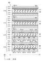
- one embodiment of the present invention aims to provide a liquid crystal optical element and lighting device that can control the light distribution direction and light distribution angle.
- a liquid crystal optical element has a first liquid crystal cell and a second liquid crystal cell overlapping the first liquid crystal cell, and each of the first liquid crystal cell and the second liquid crystal cell has a first substrate, a first electrode and a second electrode arranged on the first substrate, a second substrate arranged opposite the first substrate, a third electrode and a fourth electrode arranged on the second substrate, and a liquid crystal layer arranged between the first substrate and the second substrate, and the first electrode and the second electrode are arranged alternately in parallel to a first direction.
- the third electrodes and the fourth electrodes are alternately arranged parallel to the first direction and extend in the second direction, the first electrodes overlap with a first end of the third electrode, a space between the third electrode and the fourth electrode, and a first end of the fourth electrode in a third direction intersecting the first direction and the second direction, and the fourth electrode overlaps with a space between the first electrode and the second electrode and a first end of the second electrode in the third direction.
- a lighting device has a first liquid crystal cell and a second liquid crystal cell overlapping the first liquid crystal cell, and each of the first liquid crystal cell and the second liquid crystal cell has a first substrate, a first electrode and a second electrode arranged on the first substrate, a second substrate arranged opposite the first substrate, a third electrode and a fourth electrode arranged on the second substrate, and a liquid crystal layer arranged between the first substrate and the second substrate, and the first electrode and the second electrode are alternately arranged parallel to a first direction and extend in a second direction intersecting the first direction, and the third electrode and the fourth electrode are arranged in a first direction and in a second direction intersecting the first direction.
- the electrodes are arranged alternately parallel to the first direction and extend in the second direction, the first electrode overlaps with the first end of the third electrode, the space between the third electrode and the fourth electrode, and the first end of the fourth electrode in a third direction intersecting the first direction and the second direction, and the fourth electrode overlaps with the space between the first electrode and the second electrode and the first end of the second electrode in the third direction.
- a liquid crystal optical element and a control device electrically connected to the liquid crystal optical element and supplying control signals to the first electrode, the second electrode, the third electrode, and the fourth electrode.
- a liquid crystal optical element has a first liquid crystal cell and a second liquid crystal cell overlapping the first liquid crystal cell, and each of the first liquid crystal cell and the second liquid crystal cell has a first substrate, a first electrode and a second electrode arranged on the first substrate, a second substrate arranged opposite the first substrate, a third electrode and a fourth electrode arranged on the second substrate, and a liquid crystal layer arranged between the first substrate and the second substrate, and the first electrode and the second electrode are alternately arranged parallel to a first direction and extend in a second direction intersecting the first direction, and the The third electrode is arranged parallel to the first direction and extends in the second direction, the fourth electrode is arranged on the second substrate so as to cover the third electrode, the first electrode overlaps with a first end of the third electrode and a space between the third electrodes in a third direction intersecting the first direction and the second direction, the third electrode overlaps with a space between the first electrode and the second electrode and a first end of the second electrode in the third direction,
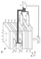
- 1 is a perspective view showing a configuration of an illumination device according to a first embodiment of the present invention.
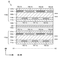
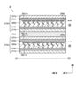
- 1 is a cross-sectional view showing a cross-sectional structure of a portion of a liquid crystal optical element according to a first embodiment of the present invention.
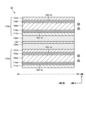
- 1 is a cross-sectional view showing a cross-sectional structure of a portion of a liquid crystal optical element according to a first embodiment of the present invention.
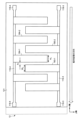
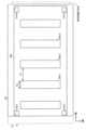
- 1 is a plan view showing an arrangement of electrodes of a liquid crystal optical element according to a first embodiment of the present invention.
- 1 is a plan view showing an arrangement of electrodes of a liquid crystal optical element according to a first embodiment of the present invention.
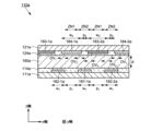
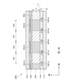
- FIG. 1 is a cross-sectional view showing a cross-sectional structure of a portion of a liquid crystal optical element according to a first embodiment of the present invention.
- 1 is a cross-sectional view for explaining light distribution using a liquid crystal optical element according to a first embodiment of the present invention.
- FIG. 1 is a cross-sectional view showing the orientation of liquid crystal in a liquid crystal layer in a liquid crystal optical element according to a first embodiment of the present invention.
- 3 is a diagram showing the relationship between each region and retardation in the liquid crystal optical element according to the first embodiment of the present invention.
- FIG. 1 is a cross-sectional view showing the orientation of liquid crystal in a liquid crystal layer in a liquid crystal optical element according to a first embodiment of the present invention.
- FIG. 13 is a perspective view showing a configuration of an illumination device according to a fourth embodiment of the present invention.
- FIG. 11 is a cross-sectional view showing a cross-sectional structure of a portion of a liquid crystal optical element according to a fourth embodiment of the present invention.
- Fig. 1 is a schematic perspective view showing the configuration of the illumination device 100.
- the first liquid crystal cell 110a and the second liquid crystal cell 110b have the same basic configuration and function. Therefore, when the first liquid crystal cell 110a and the second liquid crystal cell 110b are not distinguished, the liquid crystal cell is described as liquid crystal cell 110, and when the first liquid crystal cell 110a and the second liquid crystal cell 110b are distinguished, the liquid crystal cell is described as the first liquid crystal cell 110a and the second liquid crystal cell 110b.
- the adhesive layer 130a bonds and fixes the first liquid crystal cell 110a and the wave plate 140.
- the adhesive layer 130b bonds and fixes the wave plate 140 and the second liquid crystal cell 110b.
- the material for forming the adhesive layer 130a and the adhesive layer 130b can be an optically elastic resin.
- the optically elastic resin is, for example, an adhesive material containing an acrylic resin having translucency.
- the liquid crystal optical element 10 and the light source 30 are electrically connected to the control device 40.
- the control device 40 is electrically connected to the liquid crystal optical element 10 and the second liquid crystal cell 110b.
- the control device 40 is electrically connected via a first flexible wiring board 11a electrically connected to the terminal portion 12a of the first liquid crystal cell 110a and a second flexible wiring board 11b electrically connected to the terminal portion 12b of the second liquid crystal cell 110b.
- Light emitted from the light source 30 to the liquid crystal optical element 10 passes through the first liquid crystal cell 110a, the adhesive layer 130a, the wave plate 140, the adhesive layer 130b, and the second liquid crystal cell 110b, and is emitted from the second liquid crystal cell 110b. Details will be described later, but for example, the light passing through the liquid crystal optical element 10 is refracted in the x-axis direction or the y-axis direction based on the configuration of each electrode included in the liquid crystal cell 110 and the voltage supplied to each electrode from the control device 40.
- the lighting device 100 is capable of adjusting the light distribution direction and light distribution angle using the liquid crystal optical element 10, and can irradiate light having various adjusted light distribution directions and light distribution angles.
- FIG. 1 Configuration of the liquid crystal optical element 10
- Figures 2 and 3 are schematic cross-sectional views showing a cross-sectional structure of a portion of the liquid crystal optical element 10.
- Figure 2 is a schematic cross-sectional view in the zx plane cut along the line A1-A2 shown in Figure 1
- Figure 3 is a schematic cross-sectional view in the yz plane cut along the line B1-B2 shown in Figure 1.
- configurations that are the same as or similar to those in Figure 1 will be described as necessary.
- the first liquid crystal cell 110a includes a first substrate 111a, a second substrate 121a, a plurality of first transparent electrodes 181 (e.g., first transparent electrode 181-1a), a plurality of second transparent electrodes 182 (e.g., second transparent electrode 182-1a, second transparent electrode 182-2a), a plurality of third transparent electrodes 183 (e.g., third transparent electrode 183-1a, third transparent electrode 183-2a), a plurality of fourth transparent electrodes 184 (e.g., fourth transparent electrode 184-1a, fourth transparent electrode 184-2a), a first alignment film 114a, a second alignment film 124a, and a liquid crystal layer 160a.
- first transparent electrodes 181 e.g., first transparent electrode 181-1a
- second transparent electrode 182 e.g., second transparent electrode 182-1a, second transparent electrode 182-2a
- third transparent electrodes 183 e.g., third transparent electrode 183-1a, third transparent electrode 183-2a
- the multiple first transparent electrodes 181 and the multiple second transparent electrodes 182 are provided on the first substrate 111a and are covered with the first alignment film 114a. A portion of the first alignment film 114a is in contact with the first substrate 111a, the multiple first transparent electrodes 181, and the multiple second transparent electrodes 182.
- the plurality of third transparent electrodes 183 and the plurality of fourth transparent electrodes 184 are provided on the second substrate 121a and are covered with the second alignment film 124a. A portion of the second alignment film 124a is in contact with the second substrate 121a, the plurality of third transparent electrodes 183, and the plurality of fourth transparent electrodes 184.
- the first transparent electrode 181 and the second transparent electrode 182 on the first substrate 111a are arranged to face the third transparent electrode 183 and the fourth transparent electrode 184 on the second substrate 121a.
- a sealant (not shown) is provided around the periphery of the first substrate 111a and the second substrate 121a to bond the first substrate 111a and the second substrate 121a.
- a liquid crystal layer 160a containing liquid crystal is provided in a space surrounded by the first substrate 111a (more specifically, the first alignment film 114a), the second substrate 121a (more specifically, the second alignment film 124a), and the sealant.
- Each of the multiple first transparent electrodes 181, the multiple second transparent electrodes 182, the multiple third transparent electrodes 183, and the multiple fourth transparent electrodes 184 extends in the y-axis direction.
- the first transparent electrodes 181 and the multiple second transparent electrodes 182 are arranged alternately and repeatedly along the x-axis direction.
- the third transparent electrodes 183 and the fourth transparent electrodes 184 are arranged alternately and repeatedly along the x-axis direction.
- the first substrate 111a and the second substrate 121a may be rigid substrates having optical transparency, such as a glass substrate, a quartz substrate, or a sapphire substrate.
- the first substrate 111a and the second substrate 121a may be flexible substrates having optical transparency, such as a polyimide resin substrate, an acrylic resin substrate, a siloxane resin substrate, or a fluororesin substrate.
- the first transparent electrodes 181, the second transparent electrodes 182, the third transparent electrodes 183, and the fourth transparent electrodes 184 function as electrodes for forming an electric field in the liquid crystal layer 160a.
- the first transparent electrodes 181, the second transparent electrodes 182, the third transparent electrodes 183, and the fourth transparent electrodes 184 are made of a transparent conductive material such as indium tin oxide (ITO) or indium zinc oxide (IZO).
- the first transparent electrodes 181 provided in the first liquid crystal cell 110a and the second liquid crystal cell 110b overlap each other so that their extending directions (y-axis direction) match each other.
- the transparent electrodes of the same name provided in the first liquid crystal cell 110a and the second liquid crystal cell 110b overlap each other so that their extending directions (y-axis direction) match each other. That is, the lighting device 100 includes a configuration in which liquid crystal cells (the first liquid crystal cell 110a and the second liquid crystal cell 110b) of the same configuration are overlapped.
- the first liquid crystal cell 110a and the second liquid crystal cell 110b have the same basic configuration and function. Therefore, the first substrate 111a and the first substrate 111b, the second substrate 121a and the second substrate 121b, the plurality of first transparent electrodes 181 (e.g., the first transparent electrode 181-1a, the first transparent electrode 181-1b), the plurality of second transparent electrodes 182 (e.g., the second transparent electrode 182-1a, the second transparent electrode 182-2a, the second transparent electrode 182-1b, the second transparent electrode 182-2b), the plurality of third transparent electrodes 183 (e.g., the third transparent electrode 183-1a, the third transparent electrode 183-2a, the third transparent electrode 183-2b ...
- the plurality of first transparent electrodes 181 e.g., the first transparent electrode 181-1a, the first transparent electrode 181-1b
- the plurality of second transparent electrodes 182 e.g., the second transparent electrode 182-1a, the second transparent electrode 182-2a, the second transparent electrode 182-1b,
- the first and second alignment films 114a and 114b are used to describe the liquid crystal layers 160a and 160b.
- the components contained in the first liquid crystal cell 110a and the second liquid crystal cell 110b described above are not distinguished from one another, the components contained in the first liquid crystal cell 110a and the second liquid crystal cell 110b are described as a first substrate 111, a second substrate 121, a plurality of first transparent electrodes 181, a plurality of second transparent electrodes 182, a plurality of third transparent electrodes 183, a plurality of fourth transparent electrodes 184, a first alignment film 114, a second alignment film 124, and a liquid crystal layer 160.
- FIG. 4 is a schematic plan view showing the arrangement of a plurality of first transparent electrodes 181 and a plurality of second transparent electrodes 182 on the first substrate 111 of the liquid crystal optical element 10.
- FIG. 5 is a schematic plan view showing the arrangement of a plurality of third transparent electrodes 183 and a plurality of fourth transparent electrodes 184 on the second substrate 121 of the liquid crystal optical element 10.
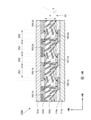
- FIG. 6 is a cross-sectional view showing a cross-sectional structure of a part of the liquid crystal optical element 10. Note that FIG. 6 corresponds to the cross-sectional structure of the first liquid crystal cell 110a taken along the line A1-A2 shown in FIG. Configurations that are the same as or similar to those in FIG. 1 to FIG. 3 will be described as necessary.
- the cross-sectional structure of the first liquid crystal cell 110a is the same as the cross-sectional structure of the second liquid crystal cell 110b, and the cross-sectional structure of the first liquid crystal cell 110a will be described here, and the cross-sectional structure of the second liquid crystal cell 110b will be described as necessary.
- each electrode of the liquid crystal optical element 10 in a planar view will be described.
- a plurality of first transparent electrodes 181, a plurality of second transparent electrodes 182, a first terminal 119-1, and a second terminal 119-2 are provided on the first substrate 111.
- a fifth wiring 116-5, a sixth wiring 116-6, a plurality of first power supply terminals 118-1, a plurality of second power supply terminals 118-2, a third terminal 119-3, and a fourth terminal 119-4 are provided on the first substrate 111.
- the multiple first transparent electrodes 181 and multiple second transparent electrodes 182 are supplied with a control signal (electric potential) from the control device 40, and have the functions of transmitting, impeding transmission of, diffusing, and refracting the light emitted from the light source 30.
- the electrode width of the first transparent electrode 181 and the electrode width of the second transparent electrode 182 are a first width w1 .
- the inter-electrode distance (electrode spacing) in the x-axis direction between the first transparent electrode 181 and the second transparent electrode 182 is a first inter-electrode distance p1.
- the first width w1 is the same as the first inter-electrode distance p1 , but the first width w1 may be different from the first inter-electrode distance p1 .
- the electrode width of the first transparent electrode 181 and the electrode width of the second transparent electrode 182 may be different.
- the plurality of first transparent electrodes 181 are electrically connected to the first wiring 116-1, and the first wiring 116-1 is electrically connected to the first terminal 119-1.
- the first wiring 116-1 may be formed under the plurality of first transparent electrodes 181, or may be formed on the plurality of first transparent electrodes 181. Also, the first wiring 116-1 may be formed in the same layer as the plurality of first transparent electrodes 181.
- the plurality of second transparent electrodes 182 are electrically connected to the second wiring 116-2, and the second wiring 116-2 is electrically connected to the second terminal 119-2.
- the second wiring 116-2 may be formed under the plurality of second transparent electrodes 182, or may be formed on the plurality of second transparent electrodes 182.
- the second wiring 116-2 may be formed in the same layer as the plurality of second transparent electrodes 182.
- the multiple first transparent electrodes 181 and multiple second transparent electrodes 182 of the lighting device 100 are formed in the same layer as the first wiring 116-1 and the second wiring 116-2.
- the first alignment film 114 disposed on the first substrate 111 is aligned in the x-axis direction (the direction indicated by the hollow arrow in FIG. 4).
- the long axes of the liquid crystal molecules on the first substrate 111 side among those constituting the liquid crystal layer 160 are aligned along the x-axis direction.
- the alignment direction of the first alignment film 114 (x-axis direction) is perpendicular to the extension direction (y-axis direction) of the multiple first transparent electrodes 181 and the multiple second transparent electrodes 182.
- a plurality of third transparent electrodes 183, a plurality of fourth transparent electrodes 184, a third wiring 116-3, a fourth wiring 116-4, a plurality of third power supply terminals 118-3, and a plurality of fourth power supply terminals 118-4 are provided on the second substrate 121.
- the plurality of third transparent electrodes 183 and the plurality of fourth transparent electrodes 184 are supplied with a control signal (electric potential) from the control device 40, and have the functions of transmitting, impeding transmission of, diffusing, and refracting the light emitted from the light source 30.
- the plurality of third transparent electrodes 183 include a third transparent electrode 183-1 and a third transparent electrode 183-2.
- the plurality of fourth transparent electrodes 184 include a fourth transparent electrode 184-1 and a fourth transparent electrode 184-2.
- the major axes of the plurality of third transparent electrodes 183 and the plurality of fourth transparent electrodes 184 extend in the y-axis direction, and the third transparent electrodes 183 and the fourth transparent electrodes 184 are alternately arranged along the x-axis direction.
- the electrode width of the third transparent electrode 183 and the electrode width of the fourth transparent electrode 184 are the second width w2 .
- the inter-electrode distance (electrode spacing) between the third transparent electrode 183 and the fourth transparent electrode 184 in the x-axis direction is the second inter-electrode distance p2 .
- the second width w2 is wider (thicker) than the first width w1
- the second inter-electrode distance p2 is narrower (thinner) than the first inter-electrode distance p1 .
- the electrode width of the third transparent electrode 183 and the electrode width of the fourth transparent electrode 184 may be different from each other.
- the plurality of third transparent electrodes 183 are electrically connected to the third wiring 116-3, and the third wiring 116-3 is electrically connected to the plurality of third power supply terminals 118-3.
- the plurality of fourth transparent electrodes 184 are electrically connected to the fourth wiring 116-4, and the fourth wiring 116-4 is electrically connected to the plurality of fourth power supply terminals 118-4.
- the third wiring 116-3 may be formed under the plurality of third transparent electrodes 183, or may be formed on the plurality of third transparent electrodes 183. Furthermore, the third wiring 116-3 may be formed in the same layer as the plurality of third transparent electrodes 183.
- the fourth wiring 116-4 may be formed under the plurality of fourth transparent electrodes 184, or may be formed on the plurality of fourth transparent electrodes 184.
- the first transparent electrodes 181 and the second transparent electrodes 182 face the third transparent electrodes 183 and the fourth transparent electrodes 184 via the liquid crystal layer 160a.
- the direction in which the first transparent electrodes 181 and the second transparent electrodes 182 extend is parallel to the direction in which the third transparent electrodes 183 and the fourth transparent electrodes 184 extend (y-axis direction).
- each of the first power supply terminals 118-1 is electrically connected to the corresponding third power supply terminal 118-3, and each of the second power supply terminals 118-2 is electrically connected to the corresponding fourth power supply terminal 118-4.
- the first wiring 116-1 is electrically connected to the third wiring 116-3
- the second wiring 116-2 is electrically connected to the fourth wiring 116-4.
- the first power supply terminal 118-1 and the third power supply terminal 118-3, and the second power supply terminal 118-2 and the fourth power supply terminal 118-4 can be electrically connected using silver paste or conductive particles.
- the conductive particles include metal-coated particles.
- the terminal portion 12a can be easily attached to the first flexible wiring board 11a and can be easily electrically connected.
- the multiple first transparent electrodes 181 are supplied with a control signal (electric potential) from the control device 40 (see FIG. 1) via the first flexible wiring board 11a, the terminal portion 12a, the first terminal 119-1, and the first wiring 116-1.
- the multiple second transparent electrodes 182 are supplied with a control signal (electric potential) from the control device 40 via the first flexible wiring board 11a, the terminal portion 12a, the second terminal 119-2, and the second wiring 116-2.
- the third transparent electrodes 183 are supplied with a control signal (electric potential) from the control device 40 via the first flexible wiring board 11a, the terminal portion 12a, the third terminal 119-3, the fifth wiring 116-5, the first power supply terminals 118-1, the third wiring 116-3, and the third power supply terminals 118-3.
- the fourth transparent electrodes 184 are supplied with a control signal (electric potential) from the control device 40 via the first flexible wiring board 11a, the terminal portion 12a, the fourth terminal 119-4, the sixth wiring 116-6, the second power supply terminals 118-2, the fourth wiring 116-4, and the fourth power supply terminals 118-4.
- each electrode in the second liquid crystal cell 110b is also supplied with a control signal (electric potential) from the control device 40.
- a photospacer may be formed on the side of the first substrate 111 facing the second substrate 121, or on the side of the second substrate 121 facing the first substrate 111. By including a photospacer, the lighting device 100 can maintain a constant distance between the first substrate 111 and the second substrate 121.
- a metal material can be used as a material for forming the first wiring 116-1, the second wiring 116-2, the third wiring 116-3, the fourth wiring 116-4, the fifth wiring 116-5, the sixth wiring 116-6, the multiple first power supply terminals 118-1, the multiple third power supply terminals 118-3, the multiple second power supply terminals 118-2, the multiple fourth power supply terminals 118-4, the first terminal 119-1, the second terminal 119-2, the third terminal 119-3, and the fourth terminal 119-4.
- the metal material is, for example, aluminum or molybdenum.
- the material forming the first transparent electrodes 181 and the second transparent electrodes 182 is ITO or IZO
- the first transparent electrodes 181 are arranged so as to overlap on the first wiring 116-1 (opposite side to the first substrate 111)
- the second transparent electrodes 182 are arranged so as to overlap on the second wiring 116-2 (opposite side to the first substrate 111).
- the material forming the first transparent electrodes 181 and the second transparent electrodes 182 is ITO or IZO
- the first transparent electrodes 181 and the second transparent electrodes 182 have high resistance to corrosion.
- first transparent electrodes 181 and multiple second transparent electrodes 182 which are highly resistant to corrosion, on the first wiring 116-1, second wiring 116-2, first terminal 119-1, and second terminal 119-2 (on the side opposite the first substrate 111) which are made of a metal material, corrosion of the first wiring 116-1, second wiring 116-2, first terminal 119-1, and second terminal 119-2 can be suppressed.
- the first transparent electrode 181-1a is sandwiched between two adjacent second transparent electrodes 182-1a and 182-2a.
- the first transparent electrode 181-1a overlaps along the z-axis direction with the end of the fourth transparent electrode 184-1a facing the third transparent electrode 183-2a, the space between the fourth transparent electrode 184-1a and the third transparent electrode 183-2a, and the end of the third transparent electrode 183-2a facing the fourth transparent electrode 184-1a.
- the space between the first transparent electrode 181-1a and the second transparent electrode 182-1a overlaps with the fourth transparent electrode 184-1a along the z-axis direction.
- the space between the first transparent electrode 181-1a and the second transparent electrode 182-2a overlaps with the third transparent electrode 183-2a along the z-axis direction.
- the second transparent electrode 182-1a overlaps along the z-axis direction with the end of the third transparent electrode 183-1a facing the fourth transparent electrode 184-1a, the space between the third transparent electrode 183-1a and the fourth transparent electrode 184-1a, and the end of the fourth transparent electrode 184-1a facing the third transparent electrode 183-1a.
- the second transparent electrode 182-2a is configured in the same manner as the second transparent electrode 182-1a.
- the third transparent electrode 183-2a is sandwiched between two adjacent fourth transparent electrodes 184-1a and 184-2a.
- the fourth transparent electrode 184-1a is sandwiched between two adjacent third transparent electrodes 183-1a and 183-2a.
- the first liquid crystal cell 110a includes a plurality of first regions ZN1 and a plurality of second regions ZN2.
- the plurality of first regions ZN1 and the plurality of second regions ZN2 are arranged alternately along the x-axis direction.
- the first region ZN1 is adjacent to the second region ZN2.
- the first region ZN1 also includes a region where the space between the first transparent electrode 181-1a and the second transparent electrode 182-1a overlaps with the fourth transparent electrode 184-1a along the z-axis direction.
- the first region ZN1 also includes a region where the space between the first transparent electrode 181-1a and the second transparent electrode 182-2a overlaps with the third transparent electrode 183-2a along the z-axis direction.
- the width OV2 is the width where the first transparent electrode 181-1a overlaps with the end of the fourth transparent electrode 184-1a on the third transparent electrode 183-2a side along the z-axis direction.
- the width OV3 is the width along the z-axis direction where the first transparent electrode 181-1a overlaps with the end of the third transparent electrode 183-2a on the fourth transparent electrode 184-1a side.
- the second region ZN2 includes, along the z-axis direction, a region where the first transparent electrode 181-1a overlaps with the end of the fourth transparent electrode 184-1a on the side of the third transparent electrode 183-2a, a region where the first transparent electrode 181-1a overlaps with the space between the fourth transparent electrode 184-1a and the third transparent electrode 183-2a, and a region where the first transparent electrode 181-1a overlaps with the end of the third transparent electrode 183-2a on the side of the fourth transparent electrode 184-1a.
- the components contained in the first liquid crystal cell 210a and the second liquid crystal cell 210b described above are not distinguished from one another, the components contained in the first liquid crystal cell 210a and the second liquid crystal cell 210b are described as a first substrate 211, a second substrate 221, a plurality of first transparent electrodes 281, a plurality of second transparent electrodes 282, a plurality of third electrodes 283, a plurality of fourth transparent electrodes 284, a first alignment film 214, a second alignment film 224, and a liquid crystal layer 260.
- the cross-sectional structure of the first liquid crystal cell 210a is the same as the cross-sectional structure of the second liquid crystal cell 210b, and the cross-sectional structure of the first liquid crystal cell 210a will be described here, and the cross-sectional structure of the second liquid crystal cell 210b will be described as necessary.
- each electrode of the liquid crystal optical element 20 in a planar view will be described.
- a plurality of first transparent electrodes 281, a plurality of second transparent electrodes 282, a first terminal 219-1, and a second terminal 219-2 are provided on the first substrate 211.
- a fifth wiring 216-5, a sixth wiring 216-6, a plurality of first power supply terminals 218-1, a plurality of second power supply terminals 218-2, and a third terminal 219-3 are provided on the first substrate 211.
- the multiple first transparent electrodes 281 and multiple second transparent electrodes 282 are supplied with a control signal (electric potential) from the control device 40, and have the functions of transmitting, impeding transmission of, diffusing, and refracting the light emitted from the light source 30.
- the fifth wiring 216-5 is electrically connected to the plurality of first power supply terminals 218-1, the sixth wiring 216-6, the plurality of second power supply terminals 218-2, and the third terminal 219-3.
- the first alignment film 214 disposed on the first substrate 211 is aligned in the x-axis direction (the direction indicated by the hollow arrow in FIG. 19).
- the long axes of the liquid crystal molecules on the first substrate 211 side among those constituting the liquid crystal layer 260 are aligned along the x-axis direction.
- the alignment direction of the first alignment film 214 (x-axis direction) is perpendicular to the extension direction (y-axis direction) of the multiple first transparent electrodes 281 and the multiple second transparent electrodes 282.
- the fourth width w4 is wider (thicker) than the third width w3
- the third inter-electrode distance p3 is narrower (thinner) than the fourth inter-electrode distance p4
- the cell gap d is narrower than the fourth width w4 .
- each of the multiple first power supply terminals 218-1 is electrically connected to the corresponding third power supply terminal 218-3
- each of the multiple second power supply terminals 218-2 is electrically connected to the corresponding fourth power supply terminal 218-4.
- the first wiring 216-1 and the sixth wiring 216-6 are electrically connected to the multiple third electrodes 283 and the fourth transparent electrode 284.
- the first power supply terminal 218-1 and the third power supply terminal 218-3, and the second power supply terminal 218-2 and the fourth power supply terminal 218-4 can be electrically connected using silver paste or conductive particles.
- the conductive particles include particles coated with a metal.
- the length of the second substrate 221 along the x-axis direction is shorter than the length of the first substrate 211 along the x-axis direction.
- the first terminal 219-1, the second terminal 219-2, and the third terminal 219-3 are provided on the terminal portion 22 on the first substrate 211.
- the first terminal 219-1, the second terminal 219-2, and the third terminal 219-3 are exposed and not covered by the second substrate 221.
- the terminal portion 22a can be easily attached to the first flexible wiring board 11a and can be easily electrically connected.
- the multiple first transparent electrodes 281 are supplied with a control signal (electric potential) from the control device 40 (see FIG. 16) via the first flexible wiring board 11a, the terminal portion 22a, the first terminal 219-1, and the first wiring 216-1.
- the multiple second transparent electrodes 282 are supplied with a control signal (electric potential) from the control device 40 via the first flexible wiring board 11a, the terminal portion 22a, the second terminal 219-2, and the second wiring 216-2.
- the third electrodes 283 and the fourth transparent electrodes 284 are supplied with a control signal (electric potential) from the control device 40 via the first flexible wiring board 11a, the terminal portion 22a, the third terminal 219-3, the fifth wiring 216-5, the first power supply terminals 218-1, the sixth wiring 216-6, the second power supply terminals 218-2, the third power supply terminals 218-3, and the fourth power supply terminals 218-4.
- the terminal portion 22b of the second liquid crystal cell 210b can also be easily attached to the second flexible wiring board 11b and easily electrically connected.
- each electrode in the second liquid crystal cell 210b is also supplied with a control signal (electric potential) from the control device 40.
- a metal material can be used as a material for forming the first wiring 216-1, the second wiring 216-2, the fifth wiring 216-5, the sixth wiring 216-6, the multiple first power supply terminals 218-1, the multiple third power supply terminals 218-3, the multiple second power supply terminals 218-2, the multiple fourth power supply terminals 218-4, the first terminal 219-1, the second terminal 219-2, the third terminal 219-3, and the multiple third electrodes 283.
- the metal material is, for example, aluminum or molybdenum.
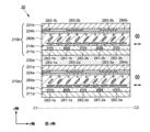
- the first transparent electrode 281-1a is sandwiched between two adjacent second transparent electrodes 282-1a and 282-2a.
- the first transparent electrode 281-1a overlaps along the z-axis direction with the end of the third electrode 283-2a on the third electrode 283-1a side, and with the space between the third electrodes 283-1a and 283-2a.
- the second transparent electrode 282-1a overlaps along the z-axis direction with the end of the third electrode 283-1a facing the third electrode 283-2a, and with the space between the third electrodes 283-1a and 283-2a.
- the first transparent electrode 281-2a is configured similarly to the first transparent electrode 281-1a.
- the second transparent electrode 282-2a and the second transparent electrode 282-3a are configured similarly to the second transparent electrode 282-1a.
- the third electrode 283-2a is sandwiched between two adjacent third electrodes 283-1a and a third transparent electrode 183-3a.
- a fourth transparent electrode 284 is disposed between the third electrodes 283-1a and 283-2a, between the third electrodes 283-2a and 283-3a, on the top surface of the third electrode 283-1a, on the top surface of the third electrode 283-2a, and on the top surface of the third electrode 283-3a.
- the first liquid crystal cell 210a includes a plurality of first regions ZN1 and a plurality of second regions ZN2.
- the plurality of first regions ZN1 and the plurality of second regions ZN2 are arranged alternately along the x-axis direction.
- the first region ZN1 is adjacent to the second region ZN2.
- the first region ZN1 also includes, along the z-axis direction, a region where the space between the first transparent electrode 281-1a and the second transparent electrode 282-1a overlaps with the space between the third electrode 283-1a and the third electrode 283-2a, a region where the space between the third electrode 283-1a and the third electrode 283-2a overlaps with the end of the first transparent electrode 281-1a on the side of the second transparent electrode 282-1a, and a region where the space between the third electrode 283-1a and the third electrode 283-2a overlaps with the end of the second transparent electrode 282-1a on the side of the first transparent electrode 281-1a.
- the first region ZN1 includes, along the z-axis direction, a region where the space between the first transparent electrode 281 and the second transparent electrode 282 overlaps with the space between adjacent third electrodes 283, a region where the space between adjacent third electrodes 283 overlaps with the end of the first transparent electrode 281, and a region where the space between adjacent third electrodes 283 overlaps with the end of the second transparent electrode 282.
- the second region ZN2 includes, along the z-axis direction, a region where the space between the first transparent electrode 281-1a and the second transparent electrode 282-2a overlaps with the opposing third electrode 283-2a, a region where the end of the first transparent electrode 281-1a on the second transparent electrode 282-2a side overlaps with the end of the opposing third electrode 283-2a on the third electrode 283-1a side, and a region where the end of the second transparent electrode 282-2a on the first transparent electrode 281-1a side overlaps with the end of the opposing third electrode 283-2a on the third electrode 283-1a side.
- the second region ZN2 includes, along the z-axis direction, a region where the space between the first transparent electrode 281 and the second transparent electrode 282 overlaps with the opposing third electrode 283, a region where the end of the first transparent electrode 281 overlaps with the opposing third electrode 283, and a region where the end of the second transparent electrode 282 overlaps with the opposing third electrode 283.
- the width OV 5 is the width at which the end of the first transparent electrode 281-1a on the second transparent electrode 282-2a side overlaps with the end of the third electrode 283-2a on the third electrode 283-1a side along the z-axis direction. Also, the width OV 5 is the width at which the end of the first transparent electrode 281-2a on the second transparent electrode 282-3a side overlaps with the end of the third electrode 283-3a on the third electrode 283-2a side along the z-axis direction. In other words, the width OV 5 is the width at which the first transparent electrode 281 overlaps with the end of the third electrode 283 along the z-axis direction.
- Width OV6 is the width at which the end of second transparent electrode 282-2a on the first transparent electrode 281-1a side overlaps with the end of third electrode 283-2a on the third electrode 283-3a side along the z-axis direction. Width OV6 is also the width at which the end of second transparent electrode 282-3a overlaps with the end of third electrode 283-3a along the z-axis direction. In other words, width OV6 is the width at which the end of second transparent electrode 282 overlaps with the end of third electrode 283.
- the cell gap d may be the distance between the surface where the liquid crystal layer 260a and the first alignment film 214a contact and the surface where the liquid crystal layer 260a and the first alignment film 214a contact, or may be the distance between the first substrate 211a and the second substrate 221a.
- the cell gap d of the lighting device 200 is the distance between the surface where the liquid crystal layer 260a and the first alignment film 214a contact and the surface where the liquid crystal layer 260a and the first alignment film 214a contact.
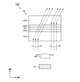
- Fig. 22 is a cross-sectional view for explaining the light distribution using the liquid crystal optical element 20.
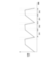
- Fig. 23 is a diagram showing the relationship between each region in the first liquid crystal cell 210a and the phase difference.
- Figs. 24 and 25 are timing charts showing the voltages supplied to each terminal included in the liquid crystal optical element 20. Configurations that are the same as or similar to those in Figs. 1 to 21 will be described as necessary.
- the liquid crystal optical element 20 will be described in a state in which a potential is supplied to each transparent electrode of the first liquid crystal cell 210a.
- the configuration and function of the second liquid crystal cell 210b are similar to those of the first liquid crystal cell 210a, and will therefore be described as necessary.
- first electric field occurs between the adjacent first transparent electrodes 281 and second transparent electrodes 282.
- the multiple third electrodes 283 and fourth transparent electrodes 284 are supplied with the same control signal (electric potential) as either the multiple first transparent electrodes 281 or the multiple second transparent electrodes 282 from the control device 40.
- the first electric field is called a transverse electric field.
- the first polarized light 61 incident on the incident surface 63 of the first liquid crystal cell 210e is bent and transmitted, rotated by 90 degrees by the wave plate 240, transmitted through the second liquid crystal cell 210f, and emitted from the liquid crystal optical element 20A. Since the second polarized light 62 is rotated 90 degrees from the first polarized light 61, it passes through the first liquid crystal cell 210e, rotates 90 degrees at the wave plate 240, is bent and passes through the second liquid crystal cell 210f in the same manner as the first polarized light 61, and is emitted from the liquid crystal optical element 20A.
- the first liquid crystal cell 210a, the adhesive layer 230a, the second liquid crystal cell 210b, the adhesive layer 230b, the third liquid crystal cell 210c, the adhesive layer 230c, and the fourth liquid crystal cell 210d are stacked in this order along the z-axis direction, starting from the side closest to the light source.
- the first liquid crystal cell 210a, the second liquid crystal cell 210b, the third liquid crystal cell 210c, and the fourth liquid crystal cell 210d have the same basic configuration and function.
- the configuration and function of the first liquid crystal cell 210a and the second liquid crystal cell 210b are similar to the configuration and function of the first liquid crystal cell 210a and the second liquid crystal cell 210b of the lighting device 200, and will be described as necessary.
- Adhesive layers 230a to 230c can be made of the same material as adhesive layer 130a.
- the light source 30 and the control device 40 have the same configuration as the lighting device 100.
- the control device 40 controls the liquid crystal optical element 20B and the light source 30.
- the control device 40 can supply control signals (electric potentials) capable of controlling the light distribution direction and orientation angle of light to the first liquid crystal cell 210a to the fourth liquid crystal cell 210d of the liquid crystal optical element 20B, and can supply control signals (electric potentials) capable of controlling the lighting and brightness of the light source 30.
- the liquid crystal optical element 20B and the light source 30 are electrically connected to the control device 40.
- the control device 40 is electrically connected via a third flexible wiring board 11c electrically connected to the terminal portion 22c of the first liquid crystal cell 210a, a second flexible wiring board 11b electrically connected to the terminal portion 22b of the second liquid crystal cell 210b, a third flexible wiring board 11c electrically connected to the terminal portion 22c of the third liquid crystal cell 210c, and a fourth flexible wiring board 11d electrically connected to the terminal portion 22d of the fourth liquid crystal cell 210d.
- Figure 29 is a schematic cross-sectional view in the zx plane taken along the line E1-E2 shown in Figure 28.
- the third liquid crystal cell 210c has the same structure and function as the first liquid crystal cell 210a
- the fourth liquid crystal cell 210d has the same structure and function as the second liquid crystal cell 210b.
- the lighting device 200B has a structure in which the liquid crystal optical element 10 (the first liquid crystal cell 210a and the second liquid crystal cell 210b having the same structure) described in the lighting device 200 is rotated 90 degrees and stacked with liquid crystal optical elements (the third liquid crystal cell 210c and the fourth liquid crystal cell 210d having the same structure) having the same structure as the liquid crystal optical element 10.
- the third liquid crystal cell 210c includes a first substrate 211c, a second substrate 221c, a plurality of first transparent electrodes (not shown), a plurality of second transparent electrodes 282 (e.g., second transparent electrode 282-1c), a plurality of third electrodes 283 (e.g., third electrode 283-1c), a fourth transparent electrode 284c, a first alignment film 214c, a second alignment film 224c, and a liquid crystal layer 260c.
- the fourth liquid crystal cell 210d includes a first substrate 211d, a second substrate 221d, a plurality of first transparent electrodes (not shown), a plurality of second transparent electrodes 282 (e.g., second transparent electrode 282-1d), a plurality of third electrodes 283 (e.g., third electrode 283-1d), a fourth transparent electrode 284d, a first alignment film 214d, a second alignment film 224d, and a liquid crystal layer 260d.
- Each component of the fourth liquid crystal cell 210d is similar to each component of the third liquid crystal cell 210c.
- the configurations of the first substrate 211c, the second substrate 221c, the plurality of first transparent electrodes 281, the plurality of second transparent electrodes 282, the first alignment film 214c, the second alignment film 224c, and the liquid crystal layer 260c are similar to the configurations of the first substrate 111a, the second substrate 121a, the plurality of first transparent electrodes 181, the plurality of second transparent electrodes 182, the first alignment film 114a, the second alignment film 124a, and the liquid crystal layer 160a. Therefore, a detailed description of the third liquid crystal cell 210c and the fourth liquid crystal cell 210d will be omitted.
- the direction in which the multiple first transparent electrodes, multiple second transparent electrodes 282, and multiple third electrodes 283 included in the third liquid crystal cell 210c and the fourth liquid crystal cell 210d extend is perpendicular to the direction in which the multiple first transparent electrodes, multiple second transparent electrodes 282, and multiple third electrodes 283 included in the first liquid crystal cell 210a and the second liquid crystal cell 210b extend.
- the direction (x-axis direction) of the alignment treatment of the first substrate 211 of the first liquid crystal cell 210a and the second liquid crystal cell 210b is perpendicular to the direction (y-axis direction) of the alignment treatment of the first substrate 211 of the third liquid crystal cell 210c and the fourth liquid crystal cell 210d.
- the direction (y-axis direction) of the alignment treatment of the second substrate 221 of the first liquid crystal cell 210a and the second liquid crystal cell 210b is perpendicular to the direction (x-axis direction) of the alignment treatment of the second substrate 221 of the third liquid crystal cell 210c and the fourth liquid crystal cell 210d.
- the first liquid crystal cell 210a bends the first polarized light 61 parallel to the y-axis direction in the x-axis direction and rotates it
- the second liquid crystal cell 210b bends the second polarized light 62 parallel to the x-axis direction in the x-axis direction and rotates it
- the third liquid crystal cell 210c bends the first polarized light 61 parallel to the y-axis direction in the y-axis direction and advances it
- the fourth liquid crystal cell 210d bends the second polarized light 62 parallel to the x-axis direction in the y-axis direction and rotates it.
- the lighting device 200B can bend light in two directions, the x-axis direction and the y-axis direction.
- the lighting device 200B can supply a potential to each electrode included in the liquid crystal optical element 20B, thereby causing light bent at a control angle ⁇ corresponding to the supplied potential to be emitted from the liquid crystal optical element 20B. Therefore, the lighting device 200B can adjust the light distribution direction and light distribution angle using the liquid crystal optical element 20B, and can irradiate light having various adjusted light distribution directions and light distribution angles.
- liquid crystal optical element and lighting device exemplified as one embodiment of the present invention may be combined as appropriate as long as they are not mutually inconsistent. Furthermore, the various configurations of the liquid crystal optical element and lighting device exemplified as one embodiment of the present invention may be interchanged as appropriate as long as they are not mutually inconsistent. Liquid crystal optical elements and lighting devices disclosed in this specification and drawings, to which a person skilled in the art has appropriately added or deleted components or modified the design, or to which a process has been added, omitted, or conditions have been changed, are also included within the scope of the present invention as long as they comprise the gist of the present invention.
Landscapes
- Physics & Mathematics (AREA)
- Nonlinear Science (AREA)
- Chemical & Material Sciences (AREA)
- Crystallography & Structural Chemistry (AREA)
- General Physics & Mathematics (AREA)
- Optics & Photonics (AREA)
- Mathematical Physics (AREA)
- Liquid Crystal (AREA)
Priority Applications (2)
| Application Number | Priority Date | Filing Date | Title |
|---|---|---|---|
| CN202480054101.9A CN121729640A (zh) | 2023-09-21 | 2024-07-19 | 液晶光学元件及照明装置 |
| JP2025547204A JPWO2025062811A1 (https=) | 2023-09-21 | 2024-07-19 |
Applications Claiming Priority (2)
| Application Number | Priority Date | Filing Date | Title |
|---|---|---|---|
| JP2023-156509 | 2023-09-21 | ||
| JP2023156509 | 2023-09-21 |
Publications (1)
| Publication Number | Publication Date |
|---|---|
| WO2025062811A1 true WO2025062811A1 (ja) | 2025-03-27 |
Family
ID=95072671
Family Applications (1)
| Application Number | Title | Priority Date | Filing Date |
|---|---|---|---|
| PCT/JP2024/025916 Pending WO2025062811A1 (ja) | 2023-09-21 | 2024-07-19 | 液晶光学素子及び照明装置 |
Country Status (3)
| Country | Link |
|---|---|
| JP (1) | JPWO2025062811A1 (https=) |
| CN (1) | CN121729640A (https=) |
| WO (1) | WO2025062811A1 (https=) |
Citations (5)
| Publication number | Priority date | Publication date | Assignee | Title |
|---|---|---|---|---|
| US20130229407A1 (en) * | 2012-03-01 | 2013-09-05 | Chunghwa Picture Tubes, Ltd. | Stereo display apparatus |
| JP2016527531A (ja) * | 2013-05-29 | 2016-09-08 | マスターイメージ 3ディー アジア リミテッド ライアビリティ カンパニー | 流動的バリアパターンを備えた立体映像表示装置 |
| WO2022176684A1 (ja) * | 2021-02-18 | 2022-08-25 | 株式会社ジャパンディスプレイ | 液晶光制御装置 |
| WO2022176360A1 (ja) * | 2021-02-18 | 2022-08-25 | 株式会社ジャパンディスプレイ | 光学素子および照明装置 |
| WO2023095459A1 (ja) * | 2021-11-25 | 2023-06-01 | 株式会社ジャパンディスプレイ | 光学素子 |
-
2024
- 2024-07-19 JP JP2025547204A patent/JPWO2025062811A1/ja active Pending
- 2024-07-19 CN CN202480054101.9A patent/CN121729640A/zh active Pending
- 2024-07-19 WO PCT/JP2024/025916 patent/WO2025062811A1/ja active Pending
Patent Citations (5)
| Publication number | Priority date | Publication date | Assignee | Title |
|---|---|---|---|---|
| US20130229407A1 (en) * | 2012-03-01 | 2013-09-05 | Chunghwa Picture Tubes, Ltd. | Stereo display apparatus |
| JP2016527531A (ja) * | 2013-05-29 | 2016-09-08 | マスターイメージ 3ディー アジア リミテッド ライアビリティ カンパニー | 流動的バリアパターンを備えた立体映像表示装置 |
| WO2022176684A1 (ja) * | 2021-02-18 | 2022-08-25 | 株式会社ジャパンディスプレイ | 液晶光制御装置 |
| WO2022176360A1 (ja) * | 2021-02-18 | 2022-08-25 | 株式会社ジャパンディスプレイ | 光学素子および照明装置 |
| WO2023095459A1 (ja) * | 2021-11-25 | 2023-06-01 | 株式会社ジャパンディスプレイ | 光学素子 |
Also Published As
| Publication number | Publication date |
|---|---|
| CN121729640A (zh) | 2026-03-24 |
| JPWO2025062811A1 (https=) | 2025-03-27 |
Similar Documents
| Publication | Publication Date | Title |
|---|---|---|
| US8111338B2 (en) | Beam shaping device | |
| US12140306B2 (en) | Optical element and lighting device | |
| CN116981985B (zh) | 液晶设备 | |
| US12422717B2 (en) | Optical element | |
| JP2024107464A (ja) | 光学素子 | |
| WO2025062811A1 (ja) | 液晶光学素子及び照明装置 | |
| US20250237910A1 (en) | Optical element and lighting device | |
| JP7496037B2 (ja) | 液晶光学素子及び照明装置 | |
| CN116964516B (zh) | 液晶设备 | |
| US12554167B2 (en) | Lighting device | |
| CN115349101A (zh) | 照明装置 | |
| CN117255966B (zh) | 液晶光学元件及照明装置 | |
| US12345985B2 (en) | Optical element | |
| US11630338B2 (en) | Display device and illumination device | |
| US20250155758A1 (en) | Optical device | |
| CN119547008A (zh) | 光学元件及包括光学元件的照明装置 | |
| CN116964516A (zh) | 液晶设备 | |
| HK40092885A (zh) | 光学元件和照明装置 | |
| CN117130180A (zh) | 光学元件以及显示装置 |
Legal Events
| Date | Code | Title | Description |
|---|---|---|---|
| 121 | Ep: the epo has been informed by wipo that ep was designated in this application |
Ref document number: 24867893 Country of ref document: EP Kind code of ref document: A1 |
|
| ENP | Entry into the national phase |
Ref document number: 2025547204 Country of ref document: JP Kind code of ref document: A |
|
| WWE | Wipo information: entry into national phase |
Ref document number: 2025547204 Country of ref document: JP |