WO2025062801A1 - 表示装置 - Google Patents
表示装置 Download PDFInfo
- Publication number
- WO2025062801A1 WO2025062801A1 PCT/JP2024/025249 JP2024025249W WO2025062801A1 WO 2025062801 A1 WO2025062801 A1 WO 2025062801A1 JP 2024025249 W JP2024025249 W JP 2024025249W WO 2025062801 A1 WO2025062801 A1 WO 2025062801A1
- Authority
- WO
- WIPO (PCT)
- Prior art keywords
- subpixel
- color filter
- light
- substrate
- display device
- Prior art date
- Legal status (The legal status is an assumption and is not a legal conclusion. Google has not performed a legal analysis and makes no representation as to the accuracy of the status listed.)
- Pending
Links
Images






Classifications
-
- G—PHYSICS
- G02—OPTICS
- G02F—OPTICAL DEVICES OR ARRANGEMENTS FOR THE CONTROL OF LIGHT BY MODIFICATION OF THE OPTICAL PROPERTIES OF THE MEDIA OF THE ELEMENTS INVOLVED THEREIN; NON-LINEAR OPTICS; FREQUENCY-CHANGING OF LIGHT; OPTICAL LOGIC ELEMENTS; OPTICAL ANALOGUE/DIGITAL CONVERTERS
- G02F1/00—Devices or arrangements for the control of the intensity, colour, phase, polarisation or direction of light arriving from an independent light source, e.g. switching, gating or modulating; Non-linear optics
- G02F1/01—Devices or arrangements for the control of the intensity, colour, phase, polarisation or direction of light arriving from an independent light source, e.g. switching, gating or modulating; Non-linear optics for the control of the intensity, phase, polarisation or colour
- G02F1/13—Devices or arrangements for the control of the intensity, colour, phase, polarisation or direction of light arriving from an independent light source, e.g. switching, gating or modulating; Non-linear optics for the control of the intensity, phase, polarisation or colour based on liquid crystals, e.g. single liquid crystal display cells
- G02F1/133—Constructional arrangements; Operation of liquid crystal cells; Circuit arrangements
- G02F1/1333—Constructional arrangements; Manufacturing methods
- G02F1/1335—Structural association of cells with optical devices, e.g. polarisers or reflectors
-
- G—PHYSICS
- G09—EDUCATION; CRYPTOGRAPHY; DISPLAY; ADVERTISING; SEALS
- G09F—DISPLAYING; ADVERTISING; SIGNS; LABELS OR NAME-PLATES; SEALS
- G09F9/00—Indicating arrangements for variable information in which the information is built-up on a support by selection or combination of individual elements
Definitions
- This disclosure relates to a display device.
- Patent document 1 discloses a display device that displays a first image in a first direction and a second image in a second direction.
- the present disclosure aims to display two images with different brightness levels on a display device that displays two images.
- the display device of the present disclosure includes a display panel having a plurality of pixels arranged in a matrix in a planar view, and a light source device that emits light toward the display panel, the pixels having a first pixel and a second pixel, the first pixel having a plurality of first subpixels having a first color filter that transmits light from the light source device, the second pixel having a plurality of second subpixels having a second color filter that transmits light from the light source device, the first color filter having a first opening, and the display panel further includes a parallax barrier having a plurality of second openings that transmit light from the light source device that has been transmitted through the first color filter and traveling along a first direction, and light from the light source device that has been transmitted through the second color filter and traveling along a second direction different from the first direction, and a light shielding portion that blocks light from the light source device that has been transmitted through the first color filter and traveling along the second direction, and light from the light source device that has been transmitted through the second color
- FIG. 1 is a conceptual diagram of a display device according to a first embodiment of the present disclosure.
- FIG. 2 is a plan view of the display device shown in FIG.
- FIG. 3 is a side view of the display device shown in FIG.
- FIG. 4 is a diagram showing an arrangement of the first subpixel and the second subpixel shown in FIG.
- FIG. 5 is a diagram showing a circuit configuration of the display panel shown in FIG.
- FIG. 6 is a cross-sectional view of the display panel shown in FIG.
- FIG. 7 is a plan view of the first color filter and the second color filter shown in FIG.
- FIG. 8 is a plan view of the parallax barrier shown in FIG. FIG.
- FIG. 9 is a diagram showing an arrangement of the first subpixels and the second subpixels in a display device according to a second embodiment of the present disclosure.
- FIG. 10 is a plan view of a parallax barrier in a display device according to a second embodiment of the present disclosure.
- FIG. 11 is a cross-sectional view of a display panel of a display device according to a modified example of the first embodiment of the present disclosure.
- FIG. 12 is a diagram showing another application example of the display device according to the embodiment of the present disclosure.
- FIG. 13 is a diagram showing another application example of the display device according to the embodiment of the present disclosure.
- FIG. 14 is a diagram showing another application example of the display device according to the embodiment of the present disclosure.
- FIG. 10 is a plan view of a parallax barrier in a display device according to a second embodiment of the present disclosure.
- FIG. 11 is a cross-sectional view of a display panel of a display device according to a modified example of the first
- FIG. 15 is a diagram showing another application example of the display device according to the embodiment of the present disclosure.
- FIG. 16 is a diagram showing another application example of the display device according to the embodiment of the present disclosure.
- FIG. 17 is a diagram showing another application example of the display device according to the embodiment of the present disclosure.
- the X and Y directions shown in the drawings are mutually orthogonal and parallel to the main surface of the substrate included in the display device 1.
- the +X side and -X side of the X direction and the +Y side and -Y side of the Y direction correspond to the sides of the display device 1.
- the Z direction is orthogonal to the X and Y directions and corresponds to the thickness direction of the display device 1.
- the +Z side of the Z direction corresponds to the front side where an image is displayed on the display device 1, and the -Z side of the Z direction corresponds to the rear side of the display device 1.
- the X, Y, and Z directions are merely examples, and the present disclosure is not limited to these directions.
- planear view refers to viewing the display device 1 from the +Z side toward the -Z side along the Z direction.
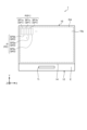
- FIG. 1 is a conceptual diagram of a display device 1 according to a first embodiment of the present disclosure.
- a first image G1 and a second image G2 are simultaneously displayed in the entire display area DA at different viewing angles.
- Fig. 1 conceptually illustrates that a first observer M1 views the first image G1, and a second observer M2 views the second image G2.
- FIG. 2 is a plan view of the display device 1 shown in FIG. 1.
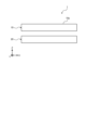
- FIG. 3 is a side view of the display device 1 shown in FIG. 2.
- the display device 1 displays an image based on an image signal output from an external device (not shown) electrically connected via a flexible wiring board (not shown).
- the display device 1 is applied to, for example, an in-vehicle display, where a first observer M1 in the driver's seat views a first image G1, and a second observer M2 in the passenger seat views a second image G2.
- the display device 1 includes a display panel 10 and a light source device 20.
- the display panel 10 is a transmissive liquid crystal display.
- the display panel 10 may be, for example, an organic EL display or an inorganic EL display.
- the display panel 10 has a display area DA on the front surface 10a where an image is displayed.
- the display panel 10 has a plurality of pixels P arranged in a matrix in a planar view.
- the row direction is parallel to the X direction.
- the column direction is parallel to the Y direction.
- the plurality of pixels P overlap the display area DA.
- the pixel P has a first pixel P1 and a second pixel P2.
- the first pixel P1 is a pixel corresponding to the first image G1.
- the first pixel P1 has a first first subpixel SP1a, a second first subpixel SP1b, and a third first subpixel SP1c.
- the first first subpixel SP1a is a red subpixel.
- the second first subpixel SP1b is a green subpixel.
- the third first subpixel SP1c is a blue subpixel.
- first subpixel SP1 when the first subpixel SP1a, the second first subpixel SP1b, and the third first subpixel SP1c are described without distinction, they will be simply referred to as the "first subpixel SP1".
- the second pixel P2 is a pixel corresponding to the second image G2.
- the second pixel P2 has a first second subpixel SP2a, a second second subpixel SP2b, and a third second subpixel SP2c.
- the first second subpixel SP2a is a red subpixel.
- the second second subpixel SP2b is a green subpixel.
- the third second subpixel SP2c is a blue subpixel.
- first second subpixel SP2a, the second second subpixel SP2b, and the third second subpixel SP2c are described without distinction, they will be simply referred to as "second subpixel SP2".
- the first pixel P1 has three first subpixels SP1
- the second pixel P2 has three second subpixels SP2. It goes without saying that the number and colors of the first subpixels SP1 and the number and colors of the second subpixels SP2 are not limited to the above numbers and colors.
- FIG. 4 is a diagram showing the arrangement of the first subpixel SP1 and the second subpixel SP2 shown in FIG. 2. Note that in FIG. 4, the first subpixel SP1 is given a rectangular shape indicated by a dashed line, and the second subpixel SP2 is given a rectangular shape indicated by a dashed line.
- the first pixel P1 and the second pixel P2 are arranged in the row direction (X direction) and the column direction (Y direction), respectively.
- the first first subpixel SP1a, the third first subpixel SP1c, and the second first subpixel SP1b are arranged repeatedly in this order.
- the second second subpixel SP2b, the first second subpixel SP2a, and the third second subpixel SP2c are arranged repeatedly in this order.
- the first subpixel SP1 and the second subpixel SP2 are rectangular, but they may also be partially curved.
- first subpixel SP1 and the second subpixel SP2 are arranged alternately along the row direction. That is, the first subpixel SP1 and the second subpixel SP2 are adjacent to each other in the row direction. Specifically, the first first subpixel SP1a is adjacent to at least one of the second second subpixel SP2b and the third second subpixel SP2c in the row direction. Furthermore, the second first subpixel SP1b is adjacent to at least one of the third second subpixel SP2c and the first second subpixel SP2a in the row direction. Furthermore, the third first subpixel SP1c is adjacent to at least one of the first second subpixel SP2a and the second second subpixel SP2b in the row direction.
- a plurality of second subpixels SP2 are arranged along the column direction. Specifically, a plurality of first second subpixels SP2a are arranged adjacent to each other along the column direction. A plurality of second second subpixels SP2b are arranged adjacent to each other along the column direction. A plurality of third second subpixels SP2c are arranged adjacent to each other along the column direction.
- the signal output circuit 11b outputs the first subpixel signal to the first subpixel SP1 and outputs the second subpixel signal to the second subpixel SP2.
- the signal output circuit 11b is electrically connected to the first subpixel SP1 and the second subpixel SP2 via multiple signal lines Lb extending along the Y direction.
- the scanning circuit 11c scans the first subpixel SP1 and the second subpixel SP2 in synchronization with the output of the first subpixel signal and the second subpixel signal by the signal output circuit 11b.
- the scanning circuit 11c is electrically connected to the first subpixel SP1 and the second subpixel SP2 via a plurality of scanning lines Lc extending along the X direction.
- an area defined by two signal lines Lb adjacent to each other in the X direction and two scanning lines Lc adjacent to each other in the Y direction corresponds to either the first subpixel SP1 or the second subpixel SP2.
- the switching element SW is composed of, for example, a thin film transistor (TFT).
- TFT thin film transistor
- the subpixel electrode PE is connected to the drain electrode of the switching element SW.
- a plurality of common electrodes CE are arranged corresponding to the plurality of scanning lines Lc.
- the subpixel electrode PE and the common electrode CE are translucent.
- FIG. 6 is a cross-sectional view of the display panel 10 shown in FIG. 2.
- the display panel 10 further includes a first substrate 12, a liquid crystal layer 13, and a second substrate 14.
- the first substrate 12, the liquid crystal layer 13, and the second substrate 14 are each light-transmitting, and are arranged in this order along the Z direction from the -Z side to the +Z side.
- the first substrate 12 and the second substrate 14 are rectangular in plan view. Note that the planar shapes of the first substrate 12 and the second substrate 14 may be shapes other than rectangular, such as circular or trapezoidal.
- a common electrode CE is disposed on the main surface 12a on the +Z side of the first substrate 12.
- An insulating layer IL is disposed in front of the common electrode CE, and a subpixel electrode PE and an alignment film AL are further disposed.
- the subpixel electrode PE is disposed between the insulating layer IL and the alignment film AL. In this manner, the common electrode CE and the subpixel electrode PE are disposed on the first substrate 12. In other words, the display panel 10 is a lateral electric field type liquid crystal display.
- the second substrate 14 is located on the front side of the first substrate 12.
- an overcoat layer OC On the back side 14b of the second substrate 14, an overcoat layer OC, a first color filter CF1, a second color filter CF2, a light-shielding film SM, and an alignment film AL are arranged.
- the light-shielding film SM, the first color filter CF1, the second color filter CF2, and the overcoat layer OC are arranged between the second substrate 14 and the alignment film AL.
- the overcoat layer OC is made of a light-transmitting material.
- the first color filter CF1 and the second color filter CF2 are disposed between the second substrate 14 and the liquid crystal layer 13.
- the first color filter CF1 is a color filter that corresponds to the first subpixel SP1.
- the second color filter CF2 is a color filter that corresponds to the second subpixel SP2.
- the first color filter CF1 and the second color filter CF2 are rectangular in plan view.
- the first color filter CF1 and the second color filter CF2 are translucent, and the spectral peak of the light that passes through them is predetermined.
- the spectral peak corresponds to the color of the first color filter CF1 and the color of the second color filter CF2.
- the light that passes through the first color filter CF1 and the second color filter CF2 is colored.
- the shapes of the first color filter CF1 and the second color filter CF2 in plan view may be changed to match the shapes of the first subpixel SP1 and the second subpixel SP2.
- the color of the first color filter CF1 is the same as the color of the first subpixel SP1.
- the color of the second color filter CF2 is the same as the color of the second subpixel SP2. That is, the first red first subpixel SP1a has a red first color filter CF1, the second green first subpixel SP1b has a green first color filter CF1, and the third blue first subpixel SP1c has a blue first color filter CF1.
- the first red second subpixel SP2a has a red second color filter CF2, the second green second subpixel SP2b has a green second color filter CF2, and the third blue second subpixel SP2c has a blue second color filter CF2.
- FIG. 7 is a plan view of the first color filter CF1 and the second color filter CF2 shown in FIG. 6.
- FIG. 7 shows the first color filter CF1 and the second color filter CF2 corresponding to one first pixel P1 and one second pixel P2.
- the first color filter CF1 has one first opening H.
- the first opening H is located in the center of the first color filter CF1 in a plan view.
- the first opening H penetrates the first color filter CF1. Therefore, the light passing through the first opening H is not colored.
- the first opening H is filled with a material forming the overcoat layer OC.
- the first color filter CF1 may have a plurality of first openings H. Furthermore, the first opening H may be located in a portion other than the center of the first color filter CF1 in a plan view.
- the light-shielding film SM has light-shielding properties, and overlaps the boundaries of the first subpixel SP1 and the boundaries of the second subpixel SP2 that are adjacent to each other in the X direction and Y direction in a planar view. That is, the light-shielding film SM overlaps the signal line Lb and the scanning line Lc in a planar view. Note that the signal line Lb and the scanning line Lc are omitted from FIG. 6. The signal line Lb and the scanning line Lc are disposed on the main surface 12a of the first substrate 12. Also, in FIG. 4, the solid line that divides the first subpixel SP1 and the second subpixel SP2 corresponds to the light-shielding film SM. Also, the periphery of the first color filter CF1 and the periphery of the second color filter CF2 overlap the light-shielding film SM in a planar view.
- the liquid crystal layer 13 shown in FIG. 6 is between the first substrate 12 and the second substrate 14.
- the liquid crystal layer 13 is composed of a plurality of liquid crystal molecules LM.
- the liquid crystal layer 13 is between the first substrate 12 and the second substrate 14, and overlaps with the display area DA in a planar view.
- the liquid crystal layer 13 is between two alignment films AL that face each other.
- the orientation of the liquid crystal molecules LM is regulated by the two alignment films AL that face each other.
- the display panel 10 further includes a first polarizing plate 15, a second polarizing plate 16, and a parallax barrier 17.
- the first polarizer 15 is disposed on the back surface 12b of the first substrate 12.
- the first polarizer 15 has a transmission axis perpendicular to the Z direction.
- the second polarizer 16 is disposed on the front surface 14a side of the second substrate 14.
- the second polarizer 16 has a transmission axis perpendicular to the transmission axis of the first polarizer 15 and the Z direction.
- the parallax barrier 17 is disposed between the second substrate 14 and the second polarizing plate 16.
- the parallax barrier 17 is disposed on the surface (front surface 14a) of the second substrate 14 opposite the surface (back surface 14b) facing the first color filter CF1 and the second color filter CF2.
- the parallax barrier 17 has a plurality of second openings 17a and light-shielding portions 17b.
- the second opening 17a transmits light that has passed through the first color filter CF1 and that travels along a first direction D1.
- the first direction D1 is a direction that is inclined from the Z direction toward the +X side in FIG. 6.
- the second opening 17a also transmits light that has passed through the second color filter CF2 and that travels along a second direction D2 that is different from the first direction D1.
- the first direction D1 is a direction that is inclined from the Z direction toward the -X side in FIG. 6. In FIG. 6, the angle between the first direction D1 and the Z direction and the angle between the second direction D2 and the Z direction are equal. Note that the angle between the first direction D1 and the Z direction and the angle between the second direction D2 and the Z direction may be different.
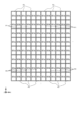
- FIG. 8 is a plan view of the parallax barrier 17 shown in FIG. 6.
- the first subpixel SP1 and the second subpixel SP2 are indicated by dashed lines.
- the second openings 17a each overlap in a plan view with the first color filter CF1 of the first subpixel SP1 and the second color filter CF2 of the second pixel P2 that are adjacent to each other in the row direction.
- the second openings 17a each overlap with the +X side of the first color filter CF1 and the -X side of the second color filter CF2.
- the second openings 17a extend along the column direction (Y direction). In a plan view, each of the second openings 17a overlaps with a plurality of first subpixels SP1 aligned along the column direction and a plurality of second subpixels SP2 aligned along the column direction. A plurality of second openings 17a are arranged along the row direction (X direction).
- the light shielding portion 17b blocks light that passes through the first color filter CF1 and travels along the second direction D2.
- the light shielding portion 17b also blocks light that passes through the second color filter CF2 and travels along the first direction D1.
- the first substrate 12 has an exposed portion E that is exposed from the second substrate 14 in a plan view.
- the exposed portion E is on the -Y side of the second substrate 14 in a plan view.
- An IC chip Ti including a drive circuit 11 is disposed on the front surface of the exposed portion E.
- the front surface of the exposed portion E is part of the main surface 12a of the first substrate 12.
- the light source device 20 is disposed on the rear side of the display panel 10.
- the light source device 20 emits light toward the display panel 10.
- the light source device 20 is, for example, a direct-type backlight, and has a plurality of light-emitting diodes (not shown).
- the display device 1 When the display device 1 receives an image signal transmitted from an external device, it displays a first image G1 and a second image G2 in the display area DA.
- the image signal includes the gradation of the first subpixel SP1 corresponding to the first image G1 and the gradation of the second subpixel SP2 corresponding to the second image G2.
- the first subpixel signal indicating the gradation of the first subpixel SP1 is output to the first subpixel SP1
- the second subpixel signal indicating the gradation of the second subpixel SP2 is output to the second subpixel SP2.
- a voltage according to the gradation indicated by the first subpixel signal is applied to the liquid crystal layer 13 corresponding to the first subpixel SP1, causing the liquid crystal molecules LM to tilt.
- the degree of tilt of the liquid crystal molecules LM changes according to the gradation indicated by the first subpixel signal.
- the light of the light source device 20 (hereinafter referred to as the emitted light) that passes through the liquid crystal layer 13 corresponding to the first subpixel SP1 is modulated to the gradation indicated by the first subpixel signal.
- the emitted light that has passed through the liquid crystal layer 13 corresponding to the first subpixel SP1 is colored by passing through the first color filter CF1.
- the light that has passed through the display panel 10 via the first color filter CF1 corresponds to the first image G1.
- the outgoing light that travels along the second direction D2 is blocked by the light-shielding portion 17b. Therefore, of the outgoing light that has passed through the first color filter CF1, the outgoing light that travels along the second direction D2 is not visible. In other words, on the side facing the second direction D2 from the display area DA, the viewer (second viewer M2 in FIG. 1) cannot view the first image G1.
- the outgoing light that passes through the first color filter CF1 and travels along the first direction D1 passes through the second opening 17a of the parallax barrier 17 and is emitted to the outside. Therefore, the outgoing light that passes through the first color filter CF1 and travels along the first direction D1 can be viewed as the first image G1. In other words, on the side facing the first direction D1 from the display area DA, the viewer (first viewer M1 in FIG. 1) can view the first image G1.
- a voltage according to the gradation indicated by the second subpixel signal is applied to the liquid crystal layer 13 corresponding to the second subpixel SP2, causing the liquid crystal molecules LM to tilt.
- the degree of tilt of the liquid crystal molecules LM changes according to the gradation indicated by the second subpixel signal.
- the outgoing light transmitted through the liquid crystal layer 13 corresponding to the second subpixel SP2 is modulated to the gradation indicated by the second subpixel signal.
- the outgoing light transmitted through the liquid crystal layer 13 corresponding to the second subpixel SP2 is colored by passing through the second color filter CF2.
- the light transmitted through the display panel 10 via the second color filter CF2 corresponds to the second image G2.
- the outgoing light that has passed through the second color filter CF2 is blocked by the light-shielding portion 17b. Therefore, of the outgoing light that has passed through the second color filter CF2, the outgoing light that travels along the first direction D1 is not visible. In other words, on the side facing the first direction D1 from the display area DA, the viewer (first viewer M1 in FIG. 1) cannot view the second image G2.
- the outgoing light that passes through the second color filter CF2 and travels along the second direction D2 passes through the second opening 17a of the parallax barrier 17 and is emitted to the outside. Therefore, the outgoing light that passes through the second color filter CF2 and travels along the second direction D2 can be viewed as the second image G2.
- the viewer on the side facing the second direction D2 from the display area DA, the viewer (second viewer M2 in FIG. 1) can view the second image G2.
- the parallax barrier 17 makes the viewing angle of the first image G1 and the viewing angle of the second image G2 different from each other. Furthermore, as described above, the first subpixel SP1 and the second subpixel SP2 are arranged throughout the entire display area DA. Therefore, the first image G1 and the second image G2 are simultaneously displayed throughout the entire display area DA.
- the second subpixel SP2 can display the color tone of the image more appropriately than the first subpixel SP1. In other words, the second image G2 is displayed in a more appropriate color tone than the first image G1.
- the display device 1 displays an image such as a movie as the second image G2, and allows the observer in the passenger seat to directly view the second image G2.
- the image of the second image G2 is viewed in an appropriate color tone by the observer in the passenger seat.
- a display device 1 according to a second embodiment of the present disclosure will be described, mainly focusing on differences from the display device 1 according to the first embodiment.
- the display device 1 according to the second embodiment differs from the display device 1 according to the first embodiment in the arrangement of the first subpixel SP1 and the second subpixel SP2, and the arrangement of the second openings 17a of the parallax barrier 17.
- FIG. 9 is a diagram showing the arrangement of the first subpixel SP1 and the second subpixel SP2 in a display device 1 according to a second embodiment of the present disclosure.
- the first pixel P1 and the second pixel P2 are each arranged along the row direction (X direction). Also, the first pixel P1 and the second pixel P2 are each arranged in a zigzag pattern along the column direction (Y direction).
- the first first subpixel SP1a, the third first subpixel SP1c, and the second first subpixel SP1b are repeatedly arranged in this order.
- the second second subpixel SP2b, the first second subpixel SP2a, and the third second subpixel SP2c are repeatedly arranged in this order.
- first subpixel SP1 and the second subpixel SP2 are arranged alternately along the row direction. That is, the first subpixel SP1 and the second subpixel SP2 are adjacent to each other in the row direction. Specifically, the first first subpixel SP1a is adjacent to at least one of the second second subpixel SP2b and the third second subpixel SP2c in the row direction. Furthermore, the second first subpixel SP1b is adjacent to at least one of the third second subpixel SP2c and the first second subpixel SP2a in the row direction. Furthermore, the third first subpixel SP1c is adjacent to at least one of the first second subpixel SP2a and the second second subpixel SP2b in the row direction.
- the first second subpixel SP2a is adjacent to at least one of the second first subpixel SP1b and the third first subpixel SP1c in the row direction. Furthermore, the second second subpixel SP2b is adjacent to at least one of the third first subpixel SP1c and the first first subpixel SP1a in the row direction. Furthermore, the third second subpixel SP2c is adjacent to at least one of the first first subpixel SP1a and the second first subpixel SP1b in the row direction.
- the first subpixel SP1 and the second subpixel SP2 are arranged alternately along the column direction. That is, the first subpixel SP1 and the second subpixel SP2 are adjacent to each other in the column direction. Specifically, the first first subpixel SP1a and the first second subpixel SP2a are arranged alternately along the column direction. The second first subpixel SP1b and the second second subpixel SP2b are arranged alternately along the column direction. The third first subpixel SP1c and the third second subpixel SP2c are arranged alternately along the column direction.
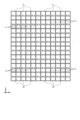
- FIG. 10 is a plan view of the parallax barrier 17 in a display device 1 according to a second embodiment of the present disclosure.
- the first subpixel SP1 and the second subpixel SP2 are indicated by dashed lines.
- each of the second openings 17a overlaps in plan with one first color filter CF1 and one second color filter CF2 that are adjacent to each other in the row direction.
- each of the second openings 17a overlaps with the +X side of the first color filter CF1 and the -X side of the second color filter CF2.
- the second openings 17a are arranged along the row direction in a plan view.
- the second openings 17a are also arranged in a zigzag pattern along the column direction in a plan view.
- the first subpixel SP1, the second subpixel SP2, and the second opening 17a are arranged as described above, so that the viewing angle of the first image G1 and the viewing angle of the second image G2 are different from each other, as in the first embodiment. Also in the second embodiment, the first subpixel SP1 and the second subpixel SP2 are arranged across the entire display area DA. Therefore, the first image G1 and the second image G2 are simultaneously displayed across the entire display area DA.
- the second opening 17a does not have to overlap at least one of the first color filter CF1 and the second color filter CF2 in a planar view.
- the second opening 17a may be formed so as to overlap one first subpixel SP1 and one second subpixel SP2 in the column direction in a planar view.
- multiple second openings 17a are arranged along both the row direction (X direction) and the column direction (Y direction).
- FIG. 11 is a cross-sectional view of a display panel 10 of a display device 1 according to a modified example of the first embodiment of the present disclosure.
- the display panel 10 of this modified example further includes a resin layer 118 between the first and second color filters CF1 and CF2 and the second substrate 14.
- the resin layer 118 is formed from a translucent resin material.
- parallax barrier 17 of this modified example is disposed between the first color filter CF1 and the second color filter CF2 and the second substrate 14.
- the parallax barrier 17 is disposed on the surface (rear surface 14b) of the second substrate 14 that faces the first color filter CF1 and the second color filter CF2.
- FIG. 12 is a diagram showing another application example of the display device 1 according to an embodiment of the present disclosure.
- the display device 1 is applied to a table 100.
- the display area DA is arranged on the top surface 100a of the table 100, and an observer sitting at the table 100 views an image.
- the orientation of the table 100 is adjusted so that an observer sitting at the table 100 facing the window can view the first image G1, and an observer sitting at the table 100 with his back to the window can view the second image G2.
- the first image G1 is brighter than the second image G2. Therefore, an observer sitting at the table 100 facing the window can properly view the first image G1.
- FIG. 13 is a diagram showing another application example of the display device 1 according to an embodiment of the present disclosure.
- the display device 1 is applied to a sign 200 to display symbols and the like.
- the sign 200 is, for example, a road sign or a guide sign.
- the image can be viewed by observers facing different directions.
- the orientation of the display device 1 is adjusted so that an observer on a side where it is difficult to view the image due to external light can view the first image G1.
- the first image G1 is brighter than the second image G2. Therefore, an observer viewing the first image G1 can properly view the information of the sign 200.
- FIG. 14 is a diagram showing another application example of the display device 1 according to an embodiment of the present disclosure.
- the display device 1 is applied to a notebook computer 300 as an example of an electronic device whose orientation can be adjusted by the observer himself/herself.
- the observer causes the desired image to be displayed in the display area DA as a first image G1, and adjusts the orientation of the electronic device so that the first image G1 can be viewed.
- the first image G1 is brighter than the second image G2. Therefore, the observer can properly view the desired image.
- the display device 1 may also be applied to a smartphone, a tablet terminal, and a television device as an electronic device whose orientation can be adjusted by the observer himself/herself.
- FIG. 15 is a diagram showing another application example of the display device 1 according to an embodiment of the present disclosure.
- the display device 1 is applied to the floor surface S of a one-way gate 400 at a railway, airport, or the like.
- a display area DA is arranged on the floor surface S of the gate 400, and an observer who is about to pass through the gate 400 sees an image.
- the orientation of the display device 1 is adjusted so that an observer on the side where passage is prohibited can see a first image G1 indicating that passage is prohibited, and an observer on the side where passage is permitted can see a second image G2 indicating that passage is permitted.
- the first image G1 is brighter than the second image G2. Therefore, an observer who sees the first image G1 can properly see that passage is prohibited.
- FIG. 16 is a diagram showing another application example of the display device 1 according to an embodiment of the present disclosure.
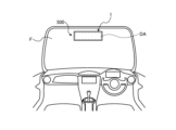
- the display device 1 is applied to a rear monitor 500 of a vehicle.
- the rear monitor 500 is arranged, for example, on the windshield F of the vehicle.
- an observer in the driver's seat and an observer in the passenger seat view the image.
- the orientation of the display device 1 is adjusted so that the observer in the driver's seat can view the image behind the vehicle as a first image G1, and the observer in the passenger seat can view his/her own image as a second image G2.
- the first image G1 is brighter than the second image G2.
- the observer in the driver's seat can properly view the image behind the vehicle even when it is difficult to view the image due to external light or at night.
- the second image G2 is displayed in a more appropriate color tone than the first image G1. Therefore, the observer in the passenger seat can view his/her own image in an appropriate color tone.
- the display device 1 is applied as a device that displays a menu on the top surface 600a of the counter 600 in a restaurant where the waiter and the customer view the menu placed on the counter 600 while facing each other across the counter 600.
- the orientation of the display device 1 is adjusted so that the waiter can view the menu as the first image G1 and the customer can view the menu as the second image G2.
- the first image G1 is brighter than the second image G2. Therefore, the waiter can properly view the information on the menu.
- the second image G2 is displayed in a more appropriate color tone than the first image G1. Therefore, the customer can properly view the menu image (e.g., the product image) in an appropriate color tone.
- REFERENCE SIGNS LIST 1 display device 10 display panel 12 first substrate 13 liquid crystal layer 14 second substrate 17 parallax barrier 17a second opening 17b light shielding portion 20 light source device CF1 first color filter CF2 second color filter D1 first direction D2 second direction DA display area H first opening P pixel P1 first pixel P2 second pixel SP1 first sub-pixel SP2 second sub-pixel
Landscapes
- Physics & Mathematics (AREA)
- Nonlinear Science (AREA)
- General Physics & Mathematics (AREA)
- Mathematical Physics (AREA)
- Chemical & Material Sciences (AREA)
- Crystallography & Structural Chemistry (AREA)
- Optics & Photonics (AREA)
- Engineering & Computer Science (AREA)
- Theoretical Computer Science (AREA)
- Devices For Indicating Variable Information By Combining Individual Elements (AREA)
Abstract
表示装置1は、複数の画素Pを有する表示パネル10を備える。画素Pは、第1カラーフィルタCF1を有する第1副画素SP1を複数有する第1画素P1、および、第2カラーフィルタCF2を有する第2副画素SP2を複数有する第2画素P2を有する。第1カラーフィルタCF1は、第1開口部Hを有する。表示パネル10は、第1カラーフィルタCF1を透過した光のうち第1方向D1に沿って進む光、および、第2カラーフィルタCF2を透過した光のうち第2方向D2に沿って進む光を通過させる複数の第2開口部17aと、第1カラーフィルタCF1を透過した光のうち第2方向D2に沿って進む光、および、第2カラーフィルタCF2を透過した光のうち第1方向D1に沿って進む光を遮る遮光部17bと、を有する視差バリア17を備える。
Description
本開示は、表示装置に関する。
特許文献1には、第1の方向に第1の画像を表示し、第2の方向に第2の画像を表示する表示装置が開示されている。
特許文献1の表示装置のように2つの画像を互いに異なる方向に向けて表示する表示装置においては、表示装置が適用されるものによって、2つの画像の明るさを互いに異なるようにしたいとの要望がある。
本開示は、2つの画像を表示する表示装置において、明るさが互いに異なる2つの画像を表示することを目的とする。
本開示の表示装置は、平面視において行列状に配置される複数の画素を有する表示パネルと、前記表示パネルに向けて光を出射する光源装置と、を備え、前記画素は、第1画素、および、第2画素を有し、前記第1画素は、前記光源装置の光を透過させる第1カラーフィルタを有する第1副画素を複数備え、前記第2画素は、前記光源装置の光を透過させる第2カラーフィルタを有する第2副画素を複数備え、前記第1カラーフィルタは、第1開口部を有し、前記表示パネルは、前記第1カラーフィルタを透過した前記光源装置の光のうち第1方向に沿って進む光、および、前記第2カラーフィルタを透過した前記光源装置の光のうち前記第1方向と異なる第2方向に沿って進む光を通過させる複数の第2開口部と、前記第1カラーフィルタを透過した前記光源装置の光のうち前記第2方向に沿って進む光、および、前記第2カラーフィルタを透過した前記光源装置の光のうち前記第1方向に沿って進む光を遮る遮光部と、を有する視差バリアをさらに備える。
以下に、本開示の各実施の形態について、図面を参照しつつ説明する。以下の実施形態に記載した内容により本開示が限定されるものではない。また、以下に記載した構成要素には、当業者が容易に想定できるもの、実質的に同一のものが含まれる。さらに、以下に記載した構成要素は適宜組み合わせることが可能である。
なお、開示はあくまで一例にすぎず、当業者において、本開示の主旨を保っての適宜変更について容易に想到し得るものについては、当然に本開示の範囲に含有されるものである。また、図面は説明をより明確にするため、実際の態様に比べ、各部の幅、厚さ、形状等について模式的に表される場合があるが、あくまで一例であって、本開示の解釈を限定するものではない。また、本明細書と各図において、既出の図に関して前述したものと同様の要素には、同一の符号を付して、詳細な説明を適宜省略することがある。
図面で示すX方向およびY方向は、互いに直交し、表示装置1に含まれる基板の主面と平行である。X方向の+X側、-X側、Y方向の+Y側、-Y側は、表示装置1の側方に相当する。Z方向は、X方向およびY方向と直交し、表示装置1の厚さ方向に相当する。Z方向の+Z側は、表示装置1において画像が表示される前面側に相当し、Z方向の-Z側は、表示装置1の背面側に相当する。なお、X、Y、Zの方向は一例であって、本開示はこれらの方向に限定されない。また、本明細書において、「平面視」はZ方向に沿って+Z側から-Z側に向かって表示装置1を見ることである。
<第1実施形態>
図1は、本開示の第1実施形態に係る表示装置1の概念図である。表示装置1の表示領域DAには、第1の画像G1および第2の画像G2が互いに異なる視野角で表示領域DAの全体に同時に表示される。図1は、第1の画像G1を第1の観察者M1が視認し、第2の画像G2を第2の観察者M2が視認することを概念的に示している。
図1は、本開示の第1実施形態に係る表示装置1の概念図である。表示装置1の表示領域DAには、第1の画像G1および第2の画像G2が互いに異なる視野角で表示領域DAの全体に同時に表示される。図1は、第1の画像G1を第1の観察者M1が視認し、第2の画像G2を第2の観察者M2が視認することを概念的に示している。
図2は、図1に示す表示装置1の平面図である。図3は、図2に示す表示装置1の側面図である。表示装置1は、フレキシブル配線基板(不図示)を介して電気的に接続される外部装置(不図示)から出力される画像信号に基づいて画像を表示する。
表示装置1は例えば車載ディスプレイに適用され、運転席の第1の観察者M1が第1の画像G1を視認し、助手席の第2の観察者M2が第2の画像G2を視認する。表示装置1は、表示パネル10、および、光源装置20を備える。
表示パネル10は、透過型の液晶ディスプレイである。なお、表示パネル10は、例えば、有機ELディスプレイおよび無機ELディスプレイでもよい。図2に示すように、表示パネル10は、画像が表示される表示領域DAを前面10aに有する。表示パネル10は、平面視において行列状に配置される複数の画素Pを有する。行方向は、X方向と平行である。列方向は、Y方向と平行である。平面視において複数の画素Pは、表示領域DAと重なる。画素Pは、第1画素P1および第2画素P2を有する。
第1画素P1は、第1の画像G1に対応する画素である。第1画素P1は、第1の第1副画素SP1a、第2の第1副画素SP1b、および、第3の第1副画素SP1cを有する。第1の第1副画素SP1aは赤の副画素である。第2の第1副画素SP1bは緑の副画素である。第3の第1副画素SP1cは青の副画素である。以下、第1の第1副画素SP1a、第2の第1副画素SP1b、および、第3の第1副画素SP1cを区別することなく説明するときは、単に「第1副画素SP1」と称する。
第2画素P2は、第2の画像G2に対応する画素である。第2画素P2は、第1の第2副画素SP2a、第2の第2副画素SP2b、および、第3の第2副画素SP2cを有する。第1の第2副画素SP2aは赤の副画素である。第2の第2副画素SP2bは緑の副画素である。第3の第2副画素SP2cは青の副画素である。以下、第1の第2副画素SP2a、第2の第2副画素SP2b、および、第3の第2副画素SP2cを区別することなく説明するときは、単に「第2副画素SP2」と称する。
このように、第1画素P1は3つの第1副画素SP1を有し、第2画素P2は3つの第2副画素SP2を有する。第1副画素SP1の個数および色、ならびに、第2副画素SP2の個数および色が上記の個数および色に限定されないことは言うまでもない。
図4は、図2に示す第1副画素SP1および第2副画素SP2の配置を示す図である。なお、図4では、第1副画素SP1には破線で示す矩形形状が付けられており、第2副画素SP2には一点鎖線で示す矩形形状が付けられている。
第1画素P1および第2画素P2は、それぞれ、行方向(X方向)および列方向(Y方向)に沿って配置される。行方向において、第1画素P1に注目すると、第1の第1副画素SP1a、第3の第1副画素SP1c、および、第2の第1副画素SP1bがこの順に繰り返し配置される。また、行方向において、第2画素P2に注目すると、第2の第2副画素SP2b、第1の第2副画素SP2a、および、第3の第2副画素SP2cがこの順に繰り返し配置される。なお、図示した例では、第1副画素SP1および第2副画素SP2は矩形状だが、一部が屈曲した形状でも良い。
さらに、第1副画素SP1および第2副画素SP2は、行方向に沿って交互に配置される。つまり、行方向において第1副画素SP1と第2副画素SP2とは互いに隣り合う。具体的には、行方向において、第1の第1副画素SP1aは、第2の第2副画素SP2bおよび第3の第2副画素SP2cの少なくとも一方と隣り合う。また、行方向において、第2の第1副画素SP1bは、第3の第2副画素SP2cおよび第1の第2副画素SP2aの少なくとも一方と隣り合う。さらに、行方向において、第3の第1副画素SP1cは、第1の第2副画素SP2aおよび第2の第2副画素SP2bの少なくとも一方と隣り合う。
そして、行方向において、第1の第2副画素SP2aは、第2の第1副画素SP1bおよび第3の第1副画素SP1cの少なくとも一方と隣り合う。また、行方向において、第2の第2副画素SP2bは、第3の第1副画素SP1cおよび第1の第1副画素SP1aの少なくとも一方と隣り合う。さらに、行方向において、第3の第2副画素SP2cは、第1の第1副画素SP1aおよび第2の第1副画素SP1bの少なくとも一方と隣り合う。
また、第1副画素SP1は、列方向に沿って複数配置される。具体的には、第1の第1副画素SP1aは、列方向に沿って互いに隣り合う状態で複数配置される。第2の第1副画素SP1bは、列方向に沿って互いに隣り合う状態で複数配置される。第3の第1副画素SP1cは、列方向に沿って互いに隣り合う状態で複数配置される。
さらに、第2副画素SP2は、列方向に沿って複数配置される。具体的には、第1の第2副画素SP2aは、列方向に沿って互いに隣り合う状態で複数配置される。第2の第2副画素SP2bは、列方向に沿って互いに隣り合う状態で複数配置される。第3の第2副画素SP2cは、列方向に沿って互いに隣り合う状態で複数配置される。
図5は、図2に示す表示パネル10の回路構成を示す図である。表示パネル10は、駆動回路11、ならびに、第1副画素SP1および第2副画素SP2それぞれが有するスイッチング素子SW、副画素電極PE、共通電極CE、液晶容量LC、および、保持容量CSを備える。第1副画素SP1および第2副画素SP2は、同様に構成される。
駆動回路11は、表示パネル10を駆動する。駆動回路11は、信号処理回路11a、信号出力回路11b、および、走査回路11cを備える。
信号処理回路11aは、外部装置から送信される画像信号に基づいて、第1副画素SP1の階調を示す第1副画素信号および第2副画素SP2の階調を示す第2副画素信号を信号出力回路11bに出力する。また、信号処理回路11aは、信号出力回路11bの動作と走査回路11cの動作とを同期させるクロック信号を信号出力回路11bおよび走査回路11cに出力する。
信号出力回路11bは、第1副画素信号を第1副画素SP1に出力し、第2副画素信号を第2副画素SP2に出力する。信号出力回路11bと第1副画素SP1および第2副画素SP2とは、Y方向に沿って延びる複数の信号線Lbを介して電気的に接続される。
走査回路11cは、信号出力回路11bによる第1副画素信号および第2副画素信号の出力と同期して、第1副画素SP1および第2副画素SP2を走査する。走査回路11cと第1副画素SP1および第2副画素SP2とは、X方向に沿って延びる複数の走査線Lcを介して電気的に接続される。
平面視においてX方向において互いに隣接する2つの信号線LbおよびY方向において互いに隣接する2つの走査線Lcによって区画される領域が第1副画素SP1および第2副画素SP2の一方に相当する。
スイッチング素子SWは、例えば薄膜トランジスタ(TFT)によって構成される。スイッチング素子SWにおいて、ソース電極と信号線Lbとが電気的に接続され、ゲート電極と走査線Lcとが電気的に接続される。
副画素電極PEは、スイッチング素子SWのドレイン電極に接続される。共通電極CEは、複数の走査線Lcに対応して複数配置される。副画素電極PEおよび共通電極CEは、透光性を有する。
液晶容量LCは、副画素電極PEと共通電極CEとの間にある後述する液晶層13の液晶材料の容量成分である。保持容量CSは、共通電極CEと同電位の電極と、副画素電極PEと同電位の電極との間にある。
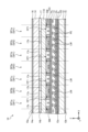
図6は、図2に示す表示パネル10の断面図である。表示パネル10は、第1基板12、液晶層13、および、第2基板14をさらに備える。第1基板12、液晶層13、および、第2基板14は、それぞれ透光性を有し、Z方向に沿って-Z側から+Z側に向けて、この順に配置される。第1基板12および第2基板14は、平面視矩形状である。なお、第1基板12および第2基板14の平面視の形状は、例えば、円形や台形状等の矩形状以外の形状であっても良い。
第1基板12の+Z側の主面12aには、共通電極CEが配置される。また、共通電極CEの前面には絶縁層ILが配置され、さらに、副画素電極PE、および、配向膜ALがさらに配置される。
副画素電極PEは、絶縁層ILと配向膜ALとの間に配置される。このように、共通電極CEと副画素電極PEは、第1基板12に配置される。つまり、表示パネル10は、横電界方式の液晶ディスプレイである。
第2基板14は、第1基板12の前面側に位置する。第2基板14の背面14b側には、オーバーコート層OC、第1カラーフィルタCF1、第2カラーフィルタCF2、遮光膜SM、および、配向膜ALが配置される。遮光膜SM、第1カラーフィルタCF1、第2カラーフィルタCF2、および、オーバーコート層OCは、第2基板14と配向膜ALとの間に配置される。
オーバーコート層OCは、透光性を有する材料によって形成される。
第1カラーフィルタCF1および第2カラーフィルタCF2は、第2基板14と液晶層13との間に配置される。第1カラーフィルタCF1は、第1副画素SP1に対応するカラーフィルタである。第2カラーフィルタCF2は、第2副画素SP2に対応するカラーフィルタである。
第1カラーフィルタCF1および第2カラーフィルタCF2は、平面視矩形状である。第1カラーフィルタCF1および第2カラーフィルタCF2は、透光性を有し、透過させる光のスペクトルのピークが予め定めされる。当該スペクトルのピークは第1カラーフィルタCF1の色および第2カラーフィルタCF2の色に対応する。つまり、第1カラーフィルタCF1および第2カラーフィルタCF2を透過する光は、着色される。なお、第1カラーフィルタCF1および第2カラーフィルタCF2の平面視の形状は、第1副画素SP1および第2副画素SP2の形状に合わせて変更しても良い。
第1カラーフィルタCF1の色は第1副画素SP1の色と同じである。第2カラーフィルタCF2の色は第2副画素SP2の色と同じである。つまり、赤の第1の第1副画素SP1aは赤の第1カラーフィルタCF1を有し、緑の第2の第1副画素SP1bは緑の第1カラーフィルタCF1を有し、青の第3の第1副画素SP1cは青の第1カラーフィルタCF1を有する。また、赤の第1の第2副画素SP2aは赤の第2カラーフィルタCF2を有し、緑の第2の第2副画素SP2bは緑の第2カラーフィルタCF2を有し、青の第3の第2副画素SP2cは青の第2カラーフィルタCF2を有する。
図7は、図6に示す第1カラーフィルタCF1および第2カラーフィルタCF2の平面図である。図7には、1つの第1画素P1および1つの第2画素P2に対応する第1カラーフィルタCF1および第2カラーフィルタCF2が示されている。図6および図7に示すように、第1カラーフィルタCF1は、第1開口部Hを1つ有する。第1開口部Hは、平面視において、第1カラーフィルタCF1の中央部に位置する。第1開口部Hは、第1カラーフィルタCF1を貫通する。よって、第1開口部Hを透過する光は、着色されない。第1開口部Hには、オーバーコート層OCを形成する材料が充填される。なお、第1カラーフィルタCF1は、第1開口部Hを複数備えてもよい。また、第1開口部Hは、平面視において、第1カラーフィルタCF1の中央部以外の部位に位置してもよい。
遮光膜SMは、遮光性を有し、X方向およびY方向において互いに隣接する第1副画素SP1の境界および第2副画素SP2の境界と平面視で重なる。すなわち、遮光膜SMは、信号線Lbおよび走査線Lcと平面視で重なる。なお、図6において、信号線Lbおよび走査線Lcの図示は省略されている。信号線Lbおよび走査線Lcは第1基板12の主面12aに配置される。また、図4において、第1副画素SP1および第2副画素SP2を区画する実線は、遮光膜SMに相当する。また、第1カラーフィルタCF1の周縁および第2カラーフィルタCF2の周縁は、平面視で遮光膜SMと重なる。
図6に示す液晶層13は、第1基板12と第2基板14との間にある。液晶層13は、複数の液晶分子LMを含んで構成される。液晶層13は、第1基板12と第2基板14との間にあり、平面視で表示領域DAと重なる。具体的には、液晶層13は、互いに対向する2つの配向膜ALの間にある。液晶分子LMの向きは、互いに対向する2つの配向膜ALによって規制される。
また、表示パネル10は、第1偏光板15、第2偏光板16、および、視差バリア17をさらに備える。
第1偏光板15は、第1基板12の背面12bに配置される。第1偏光板15は、Z方向と直交する透過軸を有する。第2偏光板16は、第2基板14の前面14a側に配置される。第2偏光板16は、第1偏光板15の透過軸およびZ方向と直交する透過軸を有する。
視差バリア17は、第2基板14と第2偏光板16との間に配置される。視差バリア17は、第2基板14において、第1カラーフィルタCF1および第2カラーフィルタCF2と対向する面(背面14b)と反対側の面(前面14a)に配置される。視差バリア17は、複数の第2開口部17a、および、遮光部17bを有する。
第2開口部17aは、第1カラーフィルタCF1を透過した光のうち第1方向D1に沿って進む光を透過する。第1方向D1は、図6においてZ方向から+X側に傾斜した方向である。また、第2開口部17aは、第2カラーフィルタCF2を透過した光のうち第1方向D1と異なる第2方向D2に沿って進む光を通過させる。第1方向D1は、図6においてZ方向から-X側に傾斜した方向である。図6において、第1方向D1とZ方向とのなす角度と第2方向D2とZ方向とのなす角度とは等しい。なお、第1方向D1とZ方向とのなす角度と、第2方向D2とZ方向とのなす角度とは異なってもよい。
図8は、図6に示す視差バリア17の平面図である。図8において、第1副画素SP1および第2副画素SP2は、破線で示されている。図6および図8に示すように、複数の第2開口部17aは、それぞれ、行方向で互いに隣り合う第1副画素SP1の第1カラーフィルタCF1および第2画素P2の第2カラーフィルタCF2と平面視で重なる。図8に示す平面視において、複数の第2開口部17aは、それぞれ、第1カラーフィルタCF1の+X側、および、第2カラーフィルタCF2の-X側と重なる。
また、図8に示すように、第2開口部17aは、列方向(Y方向)に沿って延びる形状である。複数の第2開口部17aは、それぞれ、列方向に沿って並ぶ複数の第1副画素SP1および列方向に沿って並ぶ複数の第2副画素SP2と平面視で重なる。第2開口部17aは、行方向(X方向)に沿って複数配置される。
図6および図8に示す遮光部17bは、光の吸収率が高い材料(例えば、金属クロム(Cr)、酸化クロム(CrO2)、樹脂等)で形成されている。遮光部17bは、第1カラーフィルタCF1を透過した光のうち第2方向D2に沿って進む光を遮る。また、遮光部17bは、第2カラーフィルタCF2を透過した光のうち第1方向D1に沿って進む光を遮る。
また、図2に示すように、第1基板12は、平面視で第2基板14から露出する露出部Eを有する。露出部Eは平面視で第2基板14より-Y側にある。また、露出部Eの前面には、駆動回路11を含むICチップTiが配置される。露出部Eの前面は、第1基板12の主面12aの一部である。
図3に示すように、光源装置20は、表示パネル10の背面側に配置されている。光源装置20は、表示パネル10に向けて光を出射する。光源装置20は、例えば直下型のバックライトであり、複数の発光ダイオード(不図示)を有する。
次に、表示領域DAに第1の画像G1および第2の画像G2が表示される場合の表示装置1の動作について説明する。
表示装置1は、外部装置から送信される画像信号を取得すると、第1の画像G1および第2の画像G2を表示領域DAに表示する。画像信号は、第1の画像G1に対応する第1副画素SP1の階調、および、第2の画像G2に対応する第2副画素SP2の階調を含む。上記のように第1副画素SP1の階調を示す第1副画素信号は第1副画素SP1に出力され、第2副画素SP2の階調を示す第2副画素信号は第2副画素SP2に出力される。
第1副画素信号が示す階調に応じた電圧が第1副画素SP1に対応する液晶層13に印加され、液晶分子LMが傾斜する。液晶分子LMの傾斜の度合は、第1副画素信号が示す階調に応じて変化する。第1副画素SP1に対応する液晶層13を透過する光源装置20の光(以下、出射光と称する)は第1副画素信号が示す階調に変調される。さらに、第1副画素SP1に対応する液晶層13を透過した出射光は、第1カラーフィルタCF1を透過することで着色される。第1カラーフィルタCF1を介して表示パネル10を透過した光は、第1の画像G1に相当する。
第1カラーフィルタCF1を透過した出射光のうち第2方向D2に沿って進む出射光は、遮光部17bによって遮られる。よって、第1カラーフィルタCF1を透過した出射光のうち第2方向D2に沿って進む出射光は視認不能である。つまり、表示領域DAから第2方向D2に向かう側においては、観察者(図1の第2の観察者M2)は第1の画像G1を視認することができない。
一方、第1カラーフィルタCF1を透過した出射光のうち第1方向D1に沿って進む出射光は、視差バリア17の第2開口部17aを通過して、外部に放出される。よって、第1カラーフィルタCF1を透過した出射光のうち第1方向D1に沿って進む出射光は、第1の画像G1として視認可能である。つまり、表示領域DAから第1方向D1に向かう側においては、観察者(図1の第1の観察者M1)は第1の画像G1を視認することができる。
また、第2副画素信号が示す階調に応じた電圧が第2副画素SP2に対応する液晶層13に印加され、液晶分子LMが傾斜する。液晶分子LMの傾斜の度合は、第2副画素信号が示す階調に応じて変化する。第2副画素SP2に対応する液晶層13を透過する出射光は第2副画素信号が示す階調に変調される。さらに、第2副画素SP2に対応する液晶層13を透過した出射光は、第2カラーフィルタCF2を透過することで着色される。第2カラーフィルタCF2を介して表示パネル10を透過した光は、第2の画像G2に相当する。
第2カラーフィルタCF2を透過した出射光のうち第1方向D1に沿って進む出射光は、遮光部17bによって遮られる。よって、第2カラーフィルタCF2を透過した出射光のうち第1方向D1に沿って進む出射光は視認不能である。つまり、表示領域DAから第1方向D1に向かう側においては、観察者(図1の第1の観察者M1)は第2の画像G2を視認することができない。
一方、第2カラーフィルタCF2を透過した出射光のうち第2方向D2に沿って進む出射光は、視差バリア17の第2開口部17aを通過して、外部に放出される。よって、第2カラーフィルタCF2を透過した出射光のうち第2方向D2に沿って進む出射光は、第2の画像G2として視認可能である。つまり、表示領域DAから第2方向D2に向かう側においては、観察者(図1の第2の観察者M2)は第2の画像G2を視認することができる。
このように、視差バリア17によって、第1の画像G1の視野角および第2の画像G2の視野角が互いに異なる。また、上記のように第1副画素SP1および第2副画素SP2は、表示領域DAの全体に亘って配置されている。よって、第1の画像G1および第2の画像G2は、表示領域DAの全体に同時に表示される。
また、上記のように、第1カラーフィルタCF1は、第1開口部Hを有する。よって、第1カラーフィルタCF1では、第1カラーフィルタCF1の色以外の色の出射光が第1開口部Hを介して通過する。一方、第2カラーフィルタCF2は、第1開口部Hを有さない。よって、第2カラーフィルタCF2では、第2カラーフィルタCF2の色の光のみが通過する。これにより、第1カラーフィルタCF1を通過した出射光の輝度は、第2カラーフィルタCF2を通過した出射光の輝度よりも高い。したがって、第1の画像G1は、第2の画像G2よりも明るい。このように、2つの画像を表示する表示装置1において、明るさが互いに異なる2つの画像を表示することができる。
また、上記のように、第1カラーフィルタCF1では、第1カラーフィルタCF1の色以外の色の出射光が第1開口部Hを介して通過する。一方、第2カラーフィルタCF2では、第2カラーフィルタCF2の色の出射光のみが通過する。よって、第1副画素SP1よりも、第2副画素SP2の方が画像の色調を適切に表示することができる。換言すれば、第2の画像G2は、第1の画像G1よりも適切な色調で表示される。
したがって、表示装置1が車載ディスプレイに適用される場合、表示装置1は、第1の画像G1として例えば車両の速度および車両が走行する道路の制限速度などの文字情報を表示し、運転席の観察者に視認させる。この場合、第1の画像G1の文字情報は、周囲がどのような状況でも運転席の観察者に適切に視認される。
一方、表示装置1は、第2の画像G2として例えば映画などの映像を表示し、第2の画像G2を直接的に助手席の観察者に視認させる。この場合、第2の画像G2の映像は、助手席の観察者に適切な色調で視認される。
<第2実施形態>
次に、本開示の第2実施形態に係る表示装置1について、主として上記の第1実施形態に係る表示装置1と異なる点を説明する。本第2実施形態に係る表示装置1は、第1副画素SP1および第2副画素SP2の配置、並びに、視差バリア17の第2開口部17aの配置が上記の第1実施形態の表示装置1と異なる。
次に、本開示の第2実施形態に係る表示装置1について、主として上記の第1実施形態に係る表示装置1と異なる点を説明する。本第2実施形態に係る表示装置1は、第1副画素SP1および第2副画素SP2の配置、並びに、視差バリア17の第2開口部17aの配置が上記の第1実施形態の表示装置1と異なる。
図9は、本開示の第2実施形態に係る表示装置1における第1副画素SP1および第2副画素SP2の配置を示す図である。
本第2実施形態において、第1画素P1および第2画素P2は、それぞれ、行方向(X方向)に沿って配置される。また、第1画素P1および第2画素P2は、それぞれ、列方向(Y方向)に沿ってジグザグ状に配置される。
行方向において、第1画素P1に注目すると、第1の第1副画素SP1a、第3の第1副画素SP1c、および、第2の第1副画素SP1bがこの順に繰り返し配置される。また、行方向において、第2画素P2に注目すると、第2の第2副画素SP2b、第1の第2副画素SP2a、および、第3の第2副画素SP2cがこの順に繰り返し配置される。
さらに、第1副画素SP1および第2副画素SP2は、行方向に沿って交互に配置される。つまり、行方向において第1副画素SP1と第2副画素SP2とは互いに隣り合う。具体的には、行方向において、第1の第1副画素SP1aは、第2の第2副画素SP2bおよび第3の第2副画素SP2cの少なくとも一方と隣り合う。また、行方向において、第2の第1副画素SP1bは、第3の第2副画素SP2cおよび第1の第2副画素SP2aの少なくとも一方と隣り合う。さらに、行方向において、第3の第1副画素SP1cは、第1の第2副画素SP2aおよび第2の第2副画素SP2bの少なくとも一方と隣り合う。
そして、行方向において、第1の第2副画素SP2aは、第2の第1副画素SP1bおよび第3の第1副画素SP1cの少なくとも一方と隣り合う。また、行方向において、第2の第2副画素SP2bは、第3の第1副画素SP1cおよび第1の第1副画素SP1aの少なくとも一方と隣り合う。さらに、行方向において、第3の第2副画素SP2cは、第1の第1副画素SP1aおよび第2の第1副画素SP1bの少なくとも一方と隣り合う。
また、第1副画素SP1および第2副画素SP2は、列方向に沿って交互に配置される。つまり、列方向において第1副画素SP1と第2副画素SP2とは互いに隣り合う。具体的には、第1の第1副画素SP1aおよび第1の第2副画素SP2aは、列方向に沿って交互に配置される。第2の第1副画素SP1bおよび第2の第2副画素SP2bは、列方向に沿って交互に配置される。第3の第1副画素SP1cおよび第3の第2副画素SP2cは、列方向に沿って交互に配置される。
図10は、本開示の第2実施形態に係る表示装置1における視差バリア17の平面図である。図10において、第1副画素SP1および第2副画素SP2は、破線で示されている。本第2実施形態において、複数の第2開口部17aは、それぞれ、行方向で互いに隣り合う1つの第1カラーフィルタCF1および1つの第2カラーフィルタCF2と平面視で重なる。図10に示す平面視において、上記の第1実施形態と同様に、複数の第2開口部17aは、それぞれ、第1カラーフィルタCF1の+X側、および、第2カラーフィルタCF2の-X側と重なる。
複数の第2開口部17aは、平面視において行方向に沿って配置される。また、複数の第2開口部17aは、平面視において列方向に沿ってジグザグ状に配置される。
本第2実施形態において、上記のように、第1副画素SP1、第2副画素SP2、および、第2開口部17aが配置されることで、上記の第1実施形態と同様に、第1の画像G1の視野角および第2の画像G2の視野角が互いに異なる。また、本第2実施形態においても第1副画素SP1および第2副画素SP2は、表示領域DAの全体に亘って配置されている。よって、第1の画像G1および第2の画像G2は、表示領域DAの全体に同時に表示される。
以上、本開示の好適な実施の形態を説明したが、本開示はこのような実施の形態に限定されるものではない。実施の形態で開示された内容はあくまで一例にすぎず、本開示の趣旨を逸脱しない範囲で種々の変更が可能である。本開示の趣旨を逸脱しない範囲で行われた適宜の変更についても、当然に本開示の技術的範囲に属する。
例えば、第2開口部17aは、平面視において、第1カラーフィルタCF1および第2カラーフィルタCF2の少なくとも一方と重ならなくてもよい。
また、図8に示す視差バリア17において、第2開口部17aは、列方向で1つの第1副画素SP1および1つの第2副画素SP2と平面視で重なるように形成されてもよい。この場合、第2開口部17aは、行方向(X方向)および列方向(Y方向)それぞれに沿って複数配置される。
図11は、本開示の第1実施形態の変形例に係る表示装置1の表示パネル10の断面図である。本変形例の表示パネル10は、第1カラーフィルタCF1および第2カラーフィルタCF2と第2基板14との間に樹脂層118をさらに備える。樹脂層118は、透光性を有する樹脂材料によって形成される。
また、本変形例の視差バリア17は、第1カラーフィルタCF1および第2カラーフィルタCF2と第2基板14との間に配置される。視差バリア17は、第2基板14において、第1カラーフィルタCF1および第2カラーフィルタCF2と対向する面(背面14b)に配置される。
以下、表示装置1の他の適用例について、図面を用いて説明する。
図12は、本開示の実施形態に係る表示装置1の他の適用例を示す図である。図12において、表示装置1は、テーブル100に適用される。この場合、テーブル100の天面100aに表示領域DAが配置され、テーブル100についた観察者が画像を視認する。例えば、テーブル100が窓際に配置される場合、窓に向かってテーブル100につく観察者は、外光によって画像を視認しにくい。そこで、窓に向かってテーブル100につく観察者が第1の画像G1を視認可能に、窓を背にしてテーブル100につく観察者が第2の画像G2を視認可能にテーブル100の向きを調節する。上記のように、第1の画像G1は、第2の画像G2よりも明るい。よって、窓に向かってテーブル100につく観察者は、第1の画像G1を適切に視認することができる。
図13は、本開示の実施形態に係る表示装置1の他の適用例を示す図である。図13において、表示装置1は、標識200に適用され、記号などを表示する。標識200は、例えば、道路標識および案内標識などである。この場合、向かう方向が互いに異なる観察者が画像を視認可能である。例えば、外光によって画像を視認しにくい側にいる観察者が第1の画像G1を視認可能に表示装置1の向きを調節する。上記のように、第1の画像G1は、第2の画像G2よりも明るい。よって、第1の画像G1を視認する観察者は、標識200の情報を適切に視認することができる。
図14は、本開示の実施形態に係る表示装置1の他の適用例を示す図である。図14において、表示装置1は、観察者が自ら向きを調整可能な電子機器の一例としてノートパソコン300に適用される。この場合、例えば外光によって観察者が所望の画像を視認しにくい場合に、観察者は、所望の画像を第1の画像G1として表示領域DAに表示させ、第1の画像G1を視認可能に電子機器の向きを調整する。上記のように、第1の画像G1は、第2の画像G2よりも明るい。よって、観察者は、所望の画像を適切に視認することができる。なお、表示装置1は、観察者が自ら向きを調整可能な電子機器としてスマートフォン、タブレット端末、および、テレビジョン装置に適用されてもよい。
図15は、本開示の実施形態に係る表示装置1の他の適用例を示す図である。図15において、表示装置1は、鉄道および空港などにある一方通行のゲート400の床面Sに適用される。この場合、ゲート400の床面Sに表示領域DAが配置され、ゲート400を通過しようとする観察者が画像を視認する。例えば、通行を禁止する側の観察者が通行禁止を示す第1の画像G1を視認可能に、通行可能な側の観察者が通行可能を示す第2の画像G2を視認可能に表示装置1の向きを調節する。上記のように、第1の画像G1は、第2の画像G2よりも明るい。よって、第1の画像G1を視認する観察者は、通行禁止である旨を適切に視認することができる。
図16は、本開示の実施形態に係る表示装置1の他の適用例を示す図である。図16において、表示装置1は、車両のバックモニタ500に適用される。バックモニタ500は、例えば車両のフロントガラスFに配置される。この場合、運転席の観察者および助手席の観察者が画像を視認する。例えば、運転席の観察者が車両の後方の画像を第1の画像G1として視認可能に、助手席の観察者が自身の画像を第2の画像G2として視認可能に表示装置1の向きを調節する。上記のように、第1の画像G1は、第2の画像G2よりも明るい。よって、運転席の観察者は、外光によって画像を視認しにくいときや夜間においても車両の後方の画像を適切に視認することができる。また、上記のように、第2の画像G2は、第1の画像G1よりも適切な色調で表示される。よって、助手席の観察者は、自身の画像を適切な色調で視認することができる。
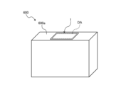
図17は、本開示の実施形態に係る表示装置1の他の適用例を示す図である。図17において、表示装置1は、店員と顧客とがカウンタ600を挟んで対面した状態で店員および顧客がカウンタ600に置かれたメニューを視認する飲食店において、カウンタ600の天面600aにメニューを表示する装置として適用される。この場合、例えば、店員がメニューを第1の画像G1として視認可能に、顧客がメニューを第2の画像G2として視認可能に表示装置1の向きを調節する。上記のように、第1の画像G1は、第2の画像G2よりも明るい。よって、店員は、メニューの情報を適切に視認することができる。また、上記のように、第2の画像G2は、第1の画像G1よりも適切な色調で表示される。よって、顧客は、メニューの画像(例えば商品の画像)を適切な色調で視認することができる。
また、本実施形態において述べた態様によりもたらされる他の作用効果について本明細書の記載から明らかなもの、又は当業者において適宜想到し得るものについては、当然に本開示によりもたらされるものと解される。
1 表示装置
10 表示パネル
12 第1基板
13 液晶層
14 第2基板
17 視差バリア
17a 第2開口部
17b 遮光部
20 光源装置
CF1 第1カラーフィルタ
CF2 第2カラーフィルタ
D1 第1方向
D2 第2方向
DA 表示領域
H 第1開口部
P 画素
P1 第1画素
P2 第2画素
SP1 第1副画素
SP2 第2副画素
10 表示パネル
12 第1基板
13 液晶層
14 第2基板
17 視差バリア
17a 第2開口部
17b 遮光部
20 光源装置
CF1 第1カラーフィルタ
CF2 第2カラーフィルタ
D1 第1方向
D2 第2方向
DA 表示領域
H 第1開口部
P 画素
P1 第1画素
P2 第2画素
SP1 第1副画素
SP2 第2副画素
Claims (7)
- 平面視において行列状に配置される複数の画素を有する表示パネルと、
前記表示パネルに向けて光を出射する光源装置と、を備え、
前記画素は、第1画素、および、第2画素を有し、
前記第1画素は、前記光源装置の光を透過させる第1カラーフィルタを有する第1副画素を複数備え、
前記第2画素は、前記光源装置の光を透過させる第2カラーフィルタを有する第2副画素を複数備え、
前記第1カラーフィルタは、第1開口部を有し、
前記表示パネルは、
前記第1カラーフィルタを透過した前記光源装置の光のうち第1方向に沿って進む光、および、前記第2カラーフィルタを透過した前記光源装置の光のうち前記第1方向と異なる第2方向に沿って進む光を通過させる複数の第2開口部と、
前記第1カラーフィルタを透過した前記光源装置の光のうち前記第2方向に沿って進む光、および、前記第2カラーフィルタを透過した前記光源装置の光のうち前記第1方向に沿って進む光を遮る遮光部と、を有する視差バリアをさらに備える、
表示装置。 - 前記第1開口部は、平面視において前記第1カラーフィルタの中央部に位置する、
請求項1に記載の表示装置。 - 前記第1副画素および前記第2副画素は、行方向に沿って交互に配置され、
複数の前記第2開口部は、それぞれ、行方向で互いに隣り合う前記第1副画素の前記第1カラーフィルタおよび前記第2副画素の前記第2カラーフィルタと平面視で重なる、
請求項1に記載の表示装置。 - 前記第1副画素および前記第2副画素は、行方向に沿って交互に配置され、
前記第1副画素は、列方向に沿って複数配置され、
前記第2副画素は、前記列方向に沿って複数配置され、
複数の前記第2開口部は、それぞれ、前記列方向に沿って並ぶ複数の前記第1副画素および前記列方向に沿って並ぶ複数の前記第2副画素と平面視で重なる、
請求項3に記載の表示装置。 - 前記第1副画素および前記第2副画素は、行方向および列方向それぞれに沿って交互に配置され、
複数の前記第2開口部は、
平面視において前記行方向に沿って配置され、
平面視において前記列方向に沿ってジグザグ状に配置される、
請求項3に記載の表示装置。 - 前記表示パネルは、
第1基板と、
第2基板と、
前記第1基板と前記第2基板との間にある液晶層と、をさらに備え、
前記第1カラーフィルタおよび前記第2カラーフィルタは、前記液晶層と前記第2基板とに間に配置され、
前記視差バリアは、前記第2基板において、前記第1カラーフィルタおよび前記第2カラーフィルタと対向する面と反対側の面に配置される、
請求項1に記載の表示装置。 - 前記表示パネルは、
第1基板と、
第2基板と、
前記第1基板と前記第2基板との間にある液晶層と、をさらに備え、
前記第1カラーフィルタおよび前記第2カラーフィルタは、前記液晶層と前記第2基板とに間に配置され、
前記視差バリアは、前記第1カラーフィルタおよび前記第2カラーフィルタと前記第2基板との間に配置される、
請求項1に記載の表示装置。
Priority Applications (1)
| Application Number | Priority Date | Filing Date | Title |
|---|---|---|---|
| CN202480059355.XA CN121866505A (zh) | 2023-09-20 | 2024-07-12 | 显示装置 |
Applications Claiming Priority (2)
| Application Number | Priority Date | Filing Date | Title |
|---|---|---|---|
| JP2023153898 | 2023-09-20 | ||
| JP2023-153898 | 2023-09-20 |
Publications (1)
| Publication Number | Publication Date |
|---|---|
| WO2025062801A1 true WO2025062801A1 (ja) | 2025-03-27 |
Family
ID=95072689
Family Applications (1)
| Application Number | Title | Priority Date | Filing Date |
|---|---|---|---|
| PCT/JP2024/025249 Pending WO2025062801A1 (ja) | 2023-09-20 | 2024-07-12 | 表示装置 |
Country Status (2)
| Country | Link |
|---|---|
| CN (1) | CN121866505A (ja) |
| WO (1) | WO2025062801A1 (ja) |
Citations (2)
| Publication number | Priority date | Publication date | Assignee | Title |
|---|---|---|---|---|
| WO2008001825A1 (fr) * | 2006-06-27 | 2008-01-03 | Nec Lcd Technologies, Ltd. | Panneau d'affichage, dispositif d'affichage, et dispositif terminal |
| JP2014190995A (ja) * | 2013-03-26 | 2014-10-06 | Japan Display Inc | 表示装置及び電子機器 |
-
2024
- 2024-07-12 WO PCT/JP2024/025249 patent/WO2025062801A1/ja active Pending
- 2024-07-12 CN CN202480059355.XA patent/CN121866505A/zh active Pending
Patent Citations (2)
| Publication number | Priority date | Publication date | Assignee | Title |
|---|---|---|---|---|
| WO2008001825A1 (fr) * | 2006-06-27 | 2008-01-03 | Nec Lcd Technologies, Ltd. | Panneau d'affichage, dispositif d'affichage, et dispositif terminal |
| JP2014190995A (ja) * | 2013-03-26 | 2014-10-06 | Japan Display Inc | 表示装置及び電子機器 |
Also Published As
| Publication number | Publication date |
|---|---|
| CN121866505A (zh) | 2026-04-14 |
Similar Documents
| Publication | Publication Date | Title |
|---|---|---|
| JP5005820B2 (ja) | 表示装置 | |
| US20180299726A1 (en) | Display device | |
| US8339331B2 (en) | Electro-optical device and electronic apparatus | |
| CN112384844A (zh) | 空中显示装置 | |
| CN102692720B (zh) | 显示装置 | |
| US20240427205A1 (en) | Display device | |
| CN113556532A (zh) | 一种显示装置 | |
| EP2518718B1 (en) | Display apparatus | |
| US7764254B2 (en) | Electro-optical device and electronic apparatus | |
| JP2008185964A (ja) | 表示装置 | |
| JP4946430B2 (ja) | 電気光学装置及び電子機器 | |
| WO2025062801A1 (ja) | 表示装置 | |
| US12393080B2 (en) | Image output panel and head-up display | |
| JP2008261980A (ja) | 液晶表示素子 | |
| JP5381423B2 (ja) | 電気光学装置および電子機器 | |
| JP2009098271A (ja) | 表示素子 | |
| CN101126882A (zh) | 液晶显示器及其液晶显示面板 | |
| CN114721191B (zh) | 显示面板及其制作方法、显示模组、显示装置 | |
| JP2008083324A (ja) | 液晶表示装置及び電子機器 | |
| CN113050334A (zh) | 液晶显示装置 | |
| US20260104587A1 (en) | Head-up display | |
| US20220206334A1 (en) | Display apparatus | |
| JP2025179396A (ja) | 表示装置 | |
| JP2010175865A (ja) | 液晶表示素子 | |
| JP2026068273A (ja) | 表示装置 |
Legal Events
| Date | Code | Title | Description |
|---|---|---|---|
| 121 | Ep: the epo has been informed by wipo that ep was designated in this application |
Ref document number: 24867884 Country of ref document: EP Kind code of ref document: A1 |
|
| ENP | Entry into the national phase |
Ref document number: 2025547200 Country of ref document: JP Kind code of ref document: A |
|
| WWE | Wipo information: entry into national phase |
Ref document number: 2025547200 Country of ref document: JP |