WO2025057743A1 - 基板処理装置及び基板処理方法 - Google Patents
基板処理装置及び基板処理方法 Download PDFInfo
- Publication number
- WO2025057743A1 WO2025057743A1 PCT/JP2024/030817 JP2024030817W WO2025057743A1 WO 2025057743 A1 WO2025057743 A1 WO 2025057743A1 JP 2024030817 W JP2024030817 W JP 2024030817W WO 2025057743 A1 WO2025057743 A1 WO 2025057743A1
- Authority
- WO
- WIPO (PCT)
- Prior art keywords
- module
- substrate
- plasma processing
- modules
- transfer
- Prior art date
- Legal status (The legal status is an assumption and is not a legal conclusion. Google has not performed a legal analysis and makes no representation as to the accuracy of the status listed.)
- Ceased
Links
Images







Classifications
-
- H—ELECTRICITY
- H10—SEMICONDUCTOR DEVICES; ELECTRIC SOLID-STATE DEVICES NOT OTHERWISE PROVIDED FOR
- H10P—GENERIC PROCESSES OR APPARATUS FOR THE MANUFACTURE OR TREATMENT OF DEVICES COVERED BY CLASS H10
- H10P72/00—Handling or holding of wafers, substrates or devices during manufacture or treatment thereof
- H10P72/04—Apparatus for manufacture or treatment
- H10P72/0451—Apparatus for manufacturing or treating in a plurality of work-stations
- H10P72/0452—Apparatus for manufacturing or treating in a plurality of work-stations characterised by the layout of the process chambers
-
- H—ELECTRICITY
- H01—ELECTRIC ELEMENTS
- H01J—ELECTRIC DISCHARGE TUBES OR DISCHARGE LAMPS
- H01J37/00—Discharge tubes with provision for introducing objects or material to be exposed to the discharge, e.g. for the purpose of examination or processing thereof
- H01J37/32—Gas-filled discharge tubes
- H01J37/32431—Constructional details of the reactor
- H01J37/32798—Further details of plasma apparatus not provided for in groups H01J37/3244 - H01J37/32788; special provisions for cleaning or maintenance of the apparatus
- H01J37/32899—Multiple chambers, e.g. cluster tools
-
- H—ELECTRICITY
- H01—ELECTRIC ELEMENTS
- H01J—ELECTRIC DISCHARGE TUBES OR DISCHARGE LAMPS
- H01J37/00—Discharge tubes with provision for introducing objects or material to be exposed to the discharge, e.g. for the purpose of examination or processing thereof
- H01J37/32—Gas-filled discharge tubes
- H01J37/32431—Constructional details of the reactor
- H01J37/32798—Further details of plasma apparatus not provided for in groups H01J37/3244 - H01J37/32788; special provisions for cleaning or maintenance of the apparatus
- H01J37/32908—Utilities
-
- H—ELECTRICITY
- H10—SEMICONDUCTOR DEVICES; ELECTRIC SOLID-STATE DEVICES NOT OTHERWISE PROVIDED FOR
- H10P—GENERIC PROCESSES OR APPARATUS FOR THE MANUFACTURE OR TREATMENT OF DEVICES COVERED BY CLASS H10
- H10P72/00—Handling or holding of wafers, substrates or devices during manufacture or treatment thereof
- H10P72/04—Apparatus for manufacture or treatment
- H10P72/0402—Apparatus for fluid treatment
- H10P72/0406—Apparatus for fluid treatment for cleaning followed by drying, rinsing, stripping, blasting or the like
- H10P72/0411—Apparatus for fluid treatment for cleaning followed by drying, rinsing, stripping, blasting or the like for wet cleaning or washing
-
- H—ELECTRICITY
- H10—SEMICONDUCTOR DEVICES; ELECTRIC SOLID-STATE DEVICES NOT OTHERWISE PROVIDED FOR
- H10P—GENERIC PROCESSES OR APPARATUS FOR THE MANUFACTURE OR TREATMENT OF DEVICES COVERED BY CLASS H10
- H10P72/00—Handling or holding of wafers, substrates or devices during manufacture or treatment thereof
- H10P72/04—Apparatus for manufacture or treatment
- H10P72/0431—Apparatus for thermal treatment
- H10P72/0432—Apparatus for thermal treatment mainly by conduction
-
- H—ELECTRICITY
- H10—SEMICONDUCTOR DEVICES; ELECTRIC SOLID-STATE DEVICES NOT OTHERWISE PROVIDED FOR
- H10P—GENERIC PROCESSES OR APPARATUS FOR THE MANUFACTURE OR TREATMENT OF DEVICES COVERED BY CLASS H10
- H10P72/00—Handling or holding of wafers, substrates or devices during manufacture or treatment thereof
- H10P72/04—Apparatus for manufacture or treatment
- H10P72/0431—Apparatus for thermal treatment
- H10P72/0434—Apparatus for thermal treatment mainly by convection
-
- H—ELECTRICITY
- H10—SEMICONDUCTOR DEVICES; ELECTRIC SOLID-STATE DEVICES NOT OTHERWISE PROVIDED FOR
- H10P—GENERIC PROCESSES OR APPARATUS FOR THE MANUFACTURE OR TREATMENT OF DEVICES COVERED BY CLASS H10
- H10P72/00—Handling or holding of wafers, substrates or devices during manufacture or treatment thereof
- H10P72/04—Apparatus for manufacture or treatment
- H10P72/0448—Apparatus for applying a liquid, a resin, an ink or the like
-
- H—ELECTRICITY
- H10—SEMICONDUCTOR DEVICES; ELECTRIC SOLID-STATE DEVICES NOT OTHERWISE PROVIDED FOR
- H10P—GENERIC PROCESSES OR APPARATUS FOR THE MANUFACTURE OR TREATMENT OF DEVICES COVERED BY CLASS H10
- H10P72/00—Handling or holding of wafers, substrates or devices during manufacture or treatment thereof
- H10P72/04—Apparatus for manufacture or treatment
- H10P72/0451—Apparatus for manufacturing or treating in a plurality of work-stations
- H10P72/0466—Apparatus for manufacturing or treating in a plurality of work-stations characterised by the construction of the load-lock chamber
-
- H—ELECTRICITY
- H10—SEMICONDUCTOR DEVICES; ELECTRIC SOLID-STATE DEVICES NOT OTHERWISE PROVIDED FOR
- H10P—GENERIC PROCESSES OR APPARATUS FOR THE MANUFACTURE OR TREATMENT OF DEVICES COVERED BY CLASS H10
- H10P72/00—Handling or holding of wafers, substrates or devices during manufacture or treatment thereof
- H10P72/04—Apparatus for manufacture or treatment
- H10P72/0451—Apparatus for manufacturing or treating in a plurality of work-stations
- H10P72/0468—Apparatus for manufacturing or treating in a plurality of work-stations comprising a chamber adapted to a particular process
-
- H—ELECTRICITY
- H10—SEMICONDUCTOR DEVICES; ELECTRIC SOLID-STATE DEVICES NOT OTHERWISE PROVIDED FOR
- H10P—GENERIC PROCESSES OR APPARATUS FOR THE MANUFACTURE OR TREATMENT OF DEVICES COVERED BY CLASS H10
- H10P72/00—Handling or holding of wafers, substrates or devices during manufacture or treatment thereof
- H10P72/30—Handling or holding of wafers, substrates or devices during manufacture or treatment thereof for conveying, e.g. between different workstations
- H10P72/33—Handling or holding of wafers, substrates or devices during manufacture or treatment thereof for conveying, e.g. between different workstations into and out of processing chamber
- H10P72/3302—Mechanical parts of transfer devices
-
- H—ELECTRICITY
- H10—SEMICONDUCTOR DEVICES; ELECTRIC SOLID-STATE DEVICES NOT OTHERWISE PROVIDED FOR
- H10P—GENERIC PROCESSES OR APPARATUS FOR THE MANUFACTURE OR TREATMENT OF DEVICES COVERED BY CLASS H10
- H10P76/00—Manufacture or treatment of masks on semiconductor bodies, e.g. by lithography or photolithography
-
- H—ELECTRICITY
- H01—ELECTRIC ELEMENTS
- H01J—ELECTRIC DISCHARGE TUBES OR DISCHARGE LAMPS
- H01J2237/00—Discharge tubes exposing object to beam, e.g. for analysis treatment, etching, imaging
- H01J2237/32—Processing objects by plasma generation
- H01J2237/33—Processing objects by plasma generation characterised by the type of processing
- H01J2237/336—Changing physical properties of treated surfaces
Definitions
- This disclosure relates to a substrate processing apparatus and a substrate processing method.
- Patent Document 1 describes a substrate processing apparatus (coating and developing apparatus) that forms a resist film, which is a coating film, and forms a pattern on the resist film by developing it after exposure.
- This disclosure provides technology related to an apparatus suitable for forming a high-quality coating film on a substrate.
- the substrate processing apparatus includes a carrier block including a carrier placement portion on which a carrier for storing a substrate is placed; a processing block including a plurality of processing modules stacked on top of each other and each processing the substrate, and a first transport mechanism shared by the plurality of processing modules and transporting the substrate, the processing block being provided on one of the left and right sides of the carrier block; a coating film forming module which constitutes one of the plurality of processing modules and supplies a coating liquid to the substrate to form a coating film; a plasma processing block provided on one side of the processing block, between which the substrate is transferred, the plasma processing block including a plurality of plasma processing modules each for plasma-processing a coating film on the substrate to modify the coating film; a second transport mechanism provided in the plasma processing block for transferring the substrate to each of the plasma processing modules and shared by the plasma processing modules; Equipped with.
- This disclosure can provide technology related to an apparatus suitable for forming a high-quality coating film on a substrate.
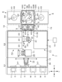
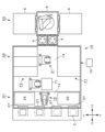
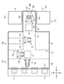
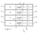
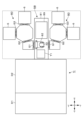
- FIG. 1 is a plan view of a substrate processing apparatus according to a first embodiment of the present disclosure.
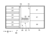
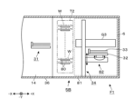
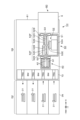
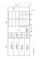
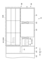
- 2 is a vertical sectional side view of the substrate processing apparatus;
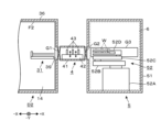
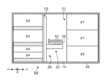
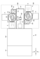
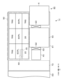
- FIG. FIG. 2 is a vertical sectional front view of the substrate processing apparatus.
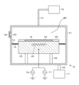
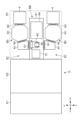
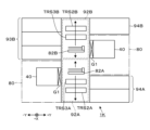
- 2 is a vertical sectional side view of a plasma processing module provided in the substrate processing apparatus;
- 4 is a flow diagram of a wafer transfer path in the substrate processing apparatus.
- FIG. 4 is a plan view showing a first modified example of the substrate processing apparatus.
- FIG. 13 is a vertical sectional front view showing a second modified example of the substrate processing apparatus.
- FIG. 13 is a vertical sectional front view showing a third modified example of the substrate processing apparatus.
- FIG. 13 is a plan view showing a fourth modified example of the substrate processing apparatus.
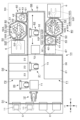
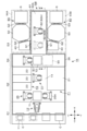
- FIG. 4 is a plan view showing a second embodiment of the substrate processing apparatus.
- FIG. 11 is a plan view showing a third embodiment of the substrate processing apparatus.
- FIG. 11 is a vertical sectional front view of the device according to the third embodiment.
- FIG. 13 is a plan view showing a fourth embodiment of the substrate processing apparatus.
- FIG. 13 is a vertical sectional front view of a modified example of the fourth embodiment.
- 11 is a vertical sectional side view showing another example of the processing block of the substrate processing apparatus.
- FIG. FIG. 13 is a plan view showing a fifth embodiment of the substrate processing apparatus.
- FIG. 13 is a vertical sectional side view of the device according to the fifth embodiment.
- FIG. 13 is a vertical sectional front view of the device according to the fifth embodiment.
- FIG. 13 is a plan view showing a modified example of the device of the fifth embodiment.
- FIG. 13 is a plan view showing a sixth embodiment of the substrate processing apparatus.
- FIG. 13 is a vertical sectional side view of the device according to the sixth embodiment.
- FIG. 13 is a vertical sectional front view showing a modified example of the device of the sixth embodiment.
- FIG. 13 is a plan view showing a seventh embodiment of the substrate processing apparatus.
- FIG. 23 is a front view of the device according to the seventh embodiment.
- FIG. 13 is a plan view showing an eighth embodiment of the substrate processing apparatus.
- FIG. 23 is a front view of the device according to the eighth embodiment.
- FIG. 23 is a vertical sectional front view of the device according to the eighth embodiment.
- FIG. 23 is a vertical sectional side view of the device according to the eighth embodiment.
- FIG. 23 is a vertical sectional front view showing a modified example of the device of the eighth embodiment.
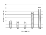
- FIG. 11 is a graph showing the results of an evaluation
- a substrate processing apparatus 1 which is a first embodiment of a substrate transfer apparatus according to the present disclosure, will be described with reference to the plan view of Fig. 1.
- the substrate processing apparatus 1 is provided in an atmospheric environment, and transfers a wafer W between modules provided within the apparatus, and performs various processes on the wafer W.
- the processes include forming a coating film by supplying a coating liquid to the wafer W in an atmospheric environment, baking the coating film by heating the wafer W in an atmospheric environment, and plasma processing the coating film after baking in a vacuum environment.
- the coating film in this example is an organic film mainly composed of carbon, called an SOC (Spin on Carbon) film.
- the manufacturing process of a semiconductor device after the formation of an SOC film will be described.
- Various films, including a resist film are formed on the SOC film.
- the resist film is then exposed and developed to form a pattern.
- the pattern is transferred to the SOC film by etching, and then the underlying film (the film formed on the underlying side of the SOC film) is etched using the SOC film as a mask. If the etching resistance of the SOC film is low, it may not be possible to form the desired mask pattern on the SOC film, or the opening of the mask pattern of the SOC film may widen during etching of the underlying film, which may prevent the pattern of the underlying film from being formed into the desired shape.
- the SOC film In order to increase the etching resistance of the SOC film, it is effective to heat the wafer W to a relatively high temperature during baking, but there are cases where such high-temperature processing is not desired. Therefore, in the substrate processing apparatus 1, the SOC film is baked at a relatively low temperature, and then the above-mentioned plasma processing is performed, thereby changing the structure of the SOC film and making it denser. This modifies the SOC film so that it has higher etching resistance.
- the substrate processing apparatus 1 is formed by connecting a carrier block D1, a processing block D2, and a plasma processing block D3 in a row horizontally.
- the direction along the row of blocks is referred to as the left-right direction, with the carrier block D1 side being the left side and the plasma processing block D3 side being the right side.
- the near side when looking at the carrier block D1 side from the left side and the plasma processing block D3 side from the right side will be referred to as the front side and the far side will be referred to as the rear side.
- the left and right sides are the -X and +X sides in the figure, respectively, and the front and rear sides are the -Y and +Y sides in the figure, respectively.
- the carrier block D1 comprises a plurality of carrier stages 11 arranged in the front-to-rear direction, and a transport mechanism 12 that transports wafers W into and out of the carriers C placed on each stage 11.
- the stages 11, which are carrier placement sections, are arranged in a front-to-rear arrangement of, for example, four stages 11.
- the carriers C are transport containers capable of storing multiple wafers W, such as a FOUP (Front Opening Unity Pod).
- a transport area 13 extending in the front-to-rear direction in a plan view is formed so that the transport mechanism 12 can access the carriers C on each stage 11, and the transport mechanism 12 moves through the transport area 13.
- Processing block D2 will be described with reference to FIG. 2, which is a longitudinal side view.
- Processing block D2 has a liquid processing unit F1 on the front side and a heating processing unit F2 on the rear side. Between the liquid processing unit F1 and the heating processing unit F2, a transfer area 14 for wafers W is configured, which extends left and right in a plan view, and the transfer area 14 is located in the center of processing block D2 in the front-to-rear direction.
- the liquid processing section F1 is formed by stacking multiple modules (liquid processing modules) that perform liquid processing on the wafer W.
- the multiple liquid processing modules include an SOC film formation module 21 and a back surface cleaning module 22.
- the liquid processing modules are provided in three stages, two of which are composed of SOC film formation modules 21 and one of which is composed of a back surface cleaning module 22.
- the SOC film formation module 21, which is a coating film formation module applies a chemical liquid (coating liquid) for forming an SOC film to the wafer W by spin coating.
- the SOC film formation module 21 is equipped with a stage on which the placed wafer W is adsorbed and held, a rotation mechanism that rotates the stage, and a nozzle that ejects the chemical liquid onto the wafer W.
- the back surface cleaning module 22 is a module that cleans the back surface of the wafer W after plasma processing, and includes a holding mechanism that contacts a portion of the back surface of the wafer W to hold the wafer W, and a back surface cleaning mechanism of the wafer W, which is composed of a nozzle, a brush, etc. that supplies a cleaning liquid.
- the cleaning mechanism cleans the portion of the back surface of the wafer W that is not held by the holding mechanism, and the holding mechanism can switch the portion it holds between the peripheral portion and the center portion of the wafer W.
- the entire back surface of the wafer W is attracted to the electrostatic chuck 64 described below, and there is a risk that foreign matter will adhere to various portions of the back surface during this attraction.
- the back surface cleaning module 22 cleans the entire back surface of the wafer W so that the foreign matter is removed.
- the heating processing unit F2 is configured by stacking a plurality of heating modules to form a laminate, and arranging a plurality of these laminates on the left and right. In this example, six heating modules form a laminate, and three of these laminates are arranged to form the heating processing unit F2.
- the heating modules that make up this heating processing unit F2 include heating modules 23 and 24.
- the heating module 23 bakes the SOC film described above. Although it has been stated that the SOC film is densified by plasma processing, the SOC film is also densified by this baking.
- the heating module 24 heats the wafer W after plasma processing to remove moisture and gas in the SOC film. In addition, the heating by this heating module 24 also plays a role in suppressing peeling of the SOC film.
- the wafer W may be exposed to a high temperature that is relatively far from the temperature at which the SOC film was baked, which may cause the SOC film to peel off, but the peeling can be suppressed by heating to an appropriate temperature by the heating module 24.
- the heating modules 23 and 24 are sometimes referred to as the pre-plasma processing heating module 23 and the post-plasma processing heating module 24 to distinguish them from each other.
- the vacuum transfer module 5 includes a housing 51 and a transfer mechanism 52 provided in the housing 51.
- An exhaust mechanism is provided to exhaust the inside of the housing 51, and the inside of the housing 51 is made into a vacuum atmosphere of a desired pressure.
- the inside of the housing 51 is a vacuum transfer area outside the load lock module 4, where the wafer W is transferred by the transfer mechanism 52.
- the transfer mechanism 52 is configured as a multi-joint arm and includes a base 52A, a first arm 52B, a second arm 52C, and a third arm 52D.
- the plasma processing module 6 includes a processing vessel 61.
- 62 denotes a transfer port provided in the side wall of the processing vessel 61.
- a stage 63 on which a wafer W is placed is provided within the processing vessel 61.
- the upper central portion of the stage 63 is configured as an electrostatic chuck 64, to which the back surface of the wafer W is attracted during plasma processing as described above.
- a focus ring 65 that surrounds the wafer W on the electrostatic chuck 64 is provided on the upper peripheral portion of the stage 63, and the distribution of the plasma formed in the processing space 60 above the wafer W is adjusted.
- a capacitively coupled plasma is formed with the ceiling of the processing vessel 61 as the upper electrode and the stage 63 as the lower electrode.
- High frequency powers of different frequencies are applied to the stage 63 from a first high frequency power supply 76 and a second high frequency power supply 77.
- the first high frequency power supply 76 is a high frequency power supply for forming plasma, and by supplying high frequency power of, for example, 100 MHz, an electric field is formed in the processing space 60 to turn the processing gas into plasma.
- the second high frequency power supply 77 is a high frequency power supply for applying a bias, and by supplying high frequency power of, for example, 400 kHz to 13 MHz, ions in the plasma are attracted toward the stage 63.
- the substrate processing apparatus 1 also includes a control unit 10.
- the control unit 10 is configured with a computer and includes a program, a memory, and a CPU.
- the program incorporates a set of steps that enable a series of operations in the substrate processing apparatus 1, which will be described later, to be performed.
- the program causes the control unit 10 to output control signals to each part of the substrate processing apparatus 1, which controls the operation of each transport mechanism and each module, thereby transporting the wafer W along the transport path, which will be described later, and processing the wafer W in each module.
- the above program is stored in a storage medium, such as a compact disc, hard disk, or DVD, and installed in the control unit 10.
- the comparative example system requires time to transport the carrier C between devices using a transport mechanism such as an OHT (Overhead Hoist Transport) installed in a semiconductor device manufacturing factory, but this transport time is not necessary in the substrate processing apparatus 1.
- OHT Overhead Hoist Transport
- the number of times that wafers W are loaded and unloaded from the carrier C to perform the series of processes described above is also less when the substrate processing apparatus 1 is used than when the comparative example system is used. Therefore, the substrate processing apparatus 1 can improve throughput.
- the wafer W may be transported in the order of pre-plasma processing heating module 23 ⁇ plasma processing module 6 ⁇ ... ⁇ back surface cleaning module 22 ⁇ post-plasma processing heating module 24, and then the wafer W may be returned to the carrier C via the transfer module TRS.
- the wafer W may also be transported in the order of pre-plasma processing heating module 23 ⁇ temperature adjustment module SCPL ⁇ plasma processing module 6 ⁇ ... ⁇ back surface cleaning module 22 ⁇ post-plasma processing heating module 24.
- the wafer W may also be transported in the order of pre-plasma processing heating module 23 ⁇ plasma processing module 6 ⁇ ... ⁇ back surface cleaning module 22 ⁇ post-plasma processing heating module 24 ⁇ temperature adjustment module SCPL.
- the order of backside cleaning of the wafer W in step S5 and heating and cooling of the wafer W in steps S6 and S7 may be arbitrary, and backside cleaning may be performed after heating and cooling in that order.
- the wafer W that has been subjected to the plasma processing in step S4 may be transported in the order of heating module 24 ⁇ temperature adjustment module SCPL ⁇ backside cleaning module 22, and then returned to the carrier C via the transfer module TRS.
- transport to the temperature adjustment module SCPL can be omitted, so the wafer W may be transported in the order of heating module 24 ⁇ backside cleaning module 22.
- the wafer W may be returned to the carrier C without performing the processing in steps S5 to S7.
- FIG. 6 shows a plan view of a substrate processing apparatus 1A which is a first modified example of the first embodiment.
- the substrate processing apparatus 1A is provided with inspection modules 25 and 26 at the front end and rear end of the transfer region 13 of the carrier block D1, respectively, so that the transfer mechanism 12 can transfer the wafer W.
- the height of the inspection modules 25 and 26 is offset from the height of the door 37 and the opening opened and closed by the door 37, and the inspection modules 25 and 26 are located above the door 37 and the opening, for example.
- the inspection modules 25 and 26 are modules that capture images of the surface (top surface) of the wafer W, and transmit the captured images to the control unit 10.
- the control unit 10 uses these images to determine whether there are any abnormalities on the surface of the wafer W, such as the presence or absence of foreign matter, and for wafers W that are determined to have abnormalities, performs processing such as transmitting the determination result to the host computer of the factory.
- pre-processing inspection module 25 and post-processing inspection module 26 take images of the wafers W before and after processing in processing block D2 and plasma processing block D3, and are therefore hereinafter referred to as pre-processing inspection module 25 and post-processing inspection module 26. It should be noted that only one of the pre-processing inspection module 25 and the post-processing inspection module 26 may be provided, or the arrangement of the pre-processing inspection module 25 and the post-processing inspection module 26 may be reversed.
- FIG. 7 shows a longitudinal sectional front view of a substrate processing apparatus 1B according to a second modification of the first embodiment.
- the right side wall of the housing 36 is formed so that the area below the gate valve G1 protrudes to the right.
- the lower side of the transfer area 14 is formed as a protruding area 83 protruding to the right from the upper side.
- stages 84 for temporarily placing the wafer W are provided in multiple stages, and the transfer mechanism 31 can transfer the wafer W to each stage 84.
- the stage 84 may be configured as a temperature adjustment module SCPL, or may be a transfer module TRS that does not have a function of adjusting the temperature of the wafer W.
- the stage 84 can be used in any manner, but can be used, for example, to hold the wafer W before it is transferred to the load lock module 4. Specifically, if the wafer W cannot be transferred to the load lock module 4 after the processing of steps S1 to S3 is completed because the load lock module 4 is changing pressure or for other reasons, the wafer W is transferred to the stage 84 to hold the wafer W. Then, when the wafer W is ready to be transferred to the load lock module 4, the wafer W is transferred from the stage 84 to the load lock module 4. In this way, it is possible to prevent the wafer W from stagnating in each processing module on the transfer path up to the load lock module 4, which would prevent the wafer W from being transferred, and thus increase the throughput of the substrate processing apparatus 1.
- the wafer W that has been subjected to plasma processing may be transported to the stage 84 and left to wait for a predetermined time before being transported to the post-plasma processing heating module 24.
- the order of the processing in the post-plasma processing heating module 24 and the processing in the back surface cleaning module 22 can be arbitrary, so the wafer W transported to the stage 84 may or may not have been subjected to back surface cleaning. Therefore, by using the stage 84 in this way, the quality of the SOC film can be further improved and a decrease in the yield of semiconductor products can be prevented.
- the substrate processing apparatus 1B described above is advantageous in that it is possible to form an area for waiting the wafer W without increasing the footprint by utilizing the area overlapping below the load lock module 4.
- a protruding area 83 may be formed in the area overlapping above, and the wafer W may be waited on.
- the load lock module 4 and the stage 84 of the protruding area 83 are arranged to overlap each other in a plan view.
- FIG. 8 shows a longitudinal sectional front view of a substrate processing apparatus 1C which is a third modified example of the first embodiment.
- a set consisting of a liquid processing section F1, a heating processing section F2 and a transport mechanism 31 described in the substrate processing apparatus 1 is stacked in two stages. These two sets are referred to as a lower stage processing section E1 and an upper stage processing section E2.
- the liquid processing section F1 of each stage is omitted in the figure.
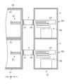
- the plasma processing block D3 is also provided in two stages, and wafers W can be transferred between the lower processing section E1 and the lower plasma processing block D3, and between the upper processing section E2 and the upper plasma processing block D3.
- transfer modules TRS and temperature adjustment modules SCPL are arranged at the respective heights of the lower processing section E1 and upper processing section E2 in the tower T1.
- FIG. 9 shows a plan view of a substrate processing apparatus 1D which is a fourth modification of the first embodiment.
- a plasma processing module 6 is also connected to the right side of the vacuum transfer module 5 via a gate valve G3. Therefore, the transfer mechanism 52 is shared by the three plasma processing modules 6.
- This configuration can increase the throughput of the apparatus.
- the substrate processing apparatus 1 is preferable from the viewpoint of further reducing the footprint.
- the substrate processing apparatus 1 may not be provided with the liquid processing unit F1, and the wafer W on which the chemical solution has been applied and the SOC film has been formed may be stored in the carrier C and transported to the substrate processing apparatus 1 by the above-mentioned factory carrier transport mechanism. Then, in the substrate processing apparatus 1, the process of step S1 described in FIG. 5 may not be performed, and the process from step S2 onwards may be performed.
- the substrate processing apparatus 1 may be configured such that only the heating module out of the heating module and liquid processing module is stacked, and the transport mechanism is shared with the heating module. Note that each of the modified examples described above can be applied not only to the substrate processing apparatus 1 of the first embodiment, but also to the substrate processing apparatuses of the other embodiments described below.
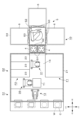
- the substrate processing apparatus 1E according to the second embodiment will be described with reference to the plan view of FIG. 10, focusing on the differences from the substrate processing apparatus 1.
- the plasma processing block D3 of the substrate processing apparatus 1E is provided with a vacuum transfer module 5A having a different shape from the vacuum transfer module 5. More specifically, the housing 51 of the vacuum transfer module 5A is longer in the front-rear direction than that of the vacuum transfer module 5.
- the front-rear width of the vacuum transfer module 5A is the same or approximately the same as the front-rear width of the carrier block D1 and the processing block D2.
- the positions of the front end and the rear end of the vacuum transfer module 5A in the front-rear direction are the same or approximately the same as the positions of the front end and the rear end of the carrier block D1 and the processing block D2, respectively.
- Three plasma processing modules 6 are connected to the right side of the vacuum transfer module 5A (the side opposite to the side to which the load lock module 4 is connected) via gate valve G3. These three plasma processing modules 6 are lined up in the front-to-rear direction with a small gap between them.
- the transfer mechanism 52 delivers wafers W to and from these three plasma processing modules 6.
- the vacuum transfer module 5A faces the processing block D2 with a gap between them.
- the load lock module 4 faces the space 85 formed between the processing block D2 and the vacuum transfer module 5.
- the space 85 corresponds to the space 19 of the substrate processing apparatus 1, and is a space where workers can enter to perform maintenance on the load lock module 4.
- This substrate processing apparatus 1E is provided with more plasma processing modules 6 than the substrate processing apparatus 1A, so that the throughput of the apparatus can be increased. Even if such a relatively large number of plasma processing modules 6 are provided, the transport mechanism 52 is shared by these plasma processing modules 6, so that the number of transport mechanisms 52 is also reduced in this substrate processing apparatus 1E, and an increase in the footprint is prevented.
- the vacuum transport modules 5 and plasma processing modules 6 of the substrate processing apparatus 1 of the first embodiment have the layout already described, the left-right width of the apparatus is smaller than that of the substrate processing apparatus 1E. Therefore, from the viewpoint of further reducing the footprint of the apparatus, the configuration of the substrate processing apparatus 1 is more advantageous.
- the substrate processing apparatus 1F of the third embodiment will be described with reference to the plan view of FIG. 11 and the vertical front view of FIG. 12, focusing on the differences from the substrate processing apparatus 1 of the first embodiment.
- an atmospheric transfer module 5B is provided on the right side of the processing block D2.
- a plasma processing module 6 is connected to a housing 81 constituting the atmospheric transfer module 5B from the front and rear via a gate valve G3.
- each plasma processing module 6 in the substrate processing apparatus 1F with respect to the processing block D2 in the front-rear direction is the same as the positional relationship of each plasma processing module 6 in the substrate processing apparatus 1 with respect to the processing block D2 in the front-rear direction.
- the plasma processing block D3 is composed of two plasma processing modules 6 and the atmospheric transfer module 5B.
- the housing 81 is connected to the right side of the processing block D2, and its interior is a transfer area for the wafer W, which is in an atmospheric atmosphere.
- the wafer W can be transferred between the processing block D2 and the atmospheric transfer module 5B through openings provided in each of the housings 81 and 36.
- the tower T2 and the transfer mechanism 82 are provided inside the housing 81.
- the tower T2 is composed of a plurality of temperature control modules SCPL and a plurality of transfer modules TRS stacked together, similar to the tower T1. In FIG. 12, the stage constituting these SCPL and TRS is indicated as 80.
- the tower T2 is located on the right side of the transfer area 14 so as to face the transfer area 14, so that the transfer mechanism 31 of the processing block D2 can transfer the wafer W to each module of the tower T2.
- Each module of the tower T2 corresponds to a placement unit, and the transfer mechanism 82 corresponds to a second transfer mechanism.
- the transfer mechanism 82 has a similar configuration to the transfer mechanism 35 provided for the tower T1, and is provided on the right side of the tower T2.
- a gate valve G3 and a plasma processing module 6 are provided on the front and rear sides of the transfer mechanism 82, respectively. Therefore, similar to the transfer mechanism 52 in the first embodiment, the transfer mechanism 82 is sandwiched between the plasma processing modules 6 from the front and rear.
- the transfer mechanism 82 can transfer wafers W to and from each module of the tower T2 and the plasma processing module 6.
- the gas supply mechanism 75 of the plasma processing module 6 of this substrate processing apparatus 1F can switch between a processing gas and the atmosphere and supply it into the processing vessel 61.
- the pressure inside the processing vessel 61 can be changed by supplying the atmosphere and exhausting the atmosphere inside the processing vessel 61, and this pressure change allows the transfer of the wafer W between the atmospheric transfer module 5B and the plasma processing module 6.
- the transfer of the wafer W between the processing block D2 and the plasma processing module 6 will be described in detail below.
- the wafer W that has been processed in the processing block D2 is transferred to the atmospheric transfer module 5B via the tower T2, and then transferred to the plasma processing module 6, where the processing vessel 61 is at atmospheric pressure.
- the processing vessel 61 is evacuated to a predetermined vacuum pressure, and plasma processing is performed on the wafer W. Then, when the pressure in the processing vessel 61 is restored to atmospheric pressure by supplying atmospheric air into the processing vessel 61, the wafer W is transferred from the plasma processing module 6 to the atmospheric transfer module 5B, and then returned to the processing block D2 via the tower T2.
- the wafer W is transported between each module for processing.
- a temperature adjustment module SCPL is also provided in the tower T2, so the wafer W may be transported to the temperature adjustment module SCPL of this tower T2 for temperature adjustment instead of the temperature adjustment module SCPL of the tower T1.
- the apparatus may be configured without the load lock module 4 and the vacuum transfer module 5.
- the substrate processing apparatus 1E is also configured to transfer the wafer W between the processing block D2 and the plasma processing module 6, and the transfer mechanism 82 is shared by the two plasma processing modules 6, so that, like the substrate processing apparatus 1, the apparatus throughput can be increased and the footprint can be reduced.
- the inside of the processing vessel 61 of the plasma processing module 6 may be relatively large since it contains structures necessary for processing the wafer W, and the time required for changing the pressure may be long depending on the volume.
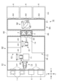
- the substrate processing apparatus 1G according to the fourth embodiment will be described with reference to the plan view of FIG. 13, focusing on the differences from the substrate processing apparatus 1F according to the third embodiment.
- the substrate processing apparatus 1G does not have the load lock module 4 and the vacuum transfer module 5 as in the substrate processing apparatus 1F, and instead has an atmospheric transfer module 5C on the right side of the processing block D2.
- the atmospheric transfer module 5C has an atmospheric atmosphere inside as in the atmospheric transfer module 5B of the substrate processing apparatus 1F.
- the atmospheric transfer module 5C is different from the atmospheric transfer module 5B in terms of the shape of the housing constituting the atmospheric transfer module 5C, the transfer mechanism provided in the housing, and the position to which the plasma processing module 6 is connected.
- the plasma processing block D3 is composed of the plasma processing module 6 and the atmospheric transfer module 5C.
- the front-rear width of the housing 88 of the atmospheric transfer module 5C is longer than the front-rear width of the housing 81 of the atmospheric transfer module 5B.
- the front-rear width of the atmospheric transfer module 5C is the same as or approximately the same as the front-rear width of the carrier block D1 and the processing block D2.
- the tower T2 and the transfer mechanism 86 are provided in this housing 88, and the transfer mechanism 86 is located on the right side of the tower T2.
- the transfer mechanism 86 has a similar configuration to the transfer mechanism 35 of the processing block D2, except that it moves linearly in the front-rear direction instead of the left-right direction by the moving mechanism 34.
- three plasma processing modules 6 are connected to the right side of the housing 88 via gate valves G3, and the plasma processing modules 6 are arranged in a front-rear direction as in the second embodiment.
- the transfer mechanism 86 can transfer wafers W to each module of the tower T2 and each plasma processing module 6.
- the wafer W is transferred along a route similar to that of the substrate processing apparatus 1F, and the pressure in the processing vessel 61 of the plasma processing module 6 is changed to transfer the wafer W between the plasma processing module 6 and the atmospheric transfer module 5C.
- the wafer W is transferred between the processing block D2 and the plasma processing module 6, and the transfer mechanism 86 is shared by the three plasma processing modules 6, so that the throughput of the apparatus can be increased and the footprint can be reduced, similar to the substrate processing apparatus 1.
- the configuration of the substrate processing apparatus 1G is preferable in consideration of the throughput of the apparatus, and the configuration of the substrate processing apparatus 1F is preferable in consideration of the footprint of the apparatus.
- the substrate processing apparatus 1G may be provided with a transport mechanism 52 which is a multi-joint arm as in the second embodiment.
- the transport mechanism 86 is configured so that the base 32 moves linearly in the forward and backward directions.
- the linear movement distance is relatively long so that the three plasma processing modules 6 can be accessed.
- the movement mechanism 34 is configured to include a drive mechanism such as a motor or a belt, and a cover that prevents particles from scattering from the drive mechanism, and the drive mechanism and the base 32 are connected via a connection part. As described above, if the linear movement distance of the base 32 is long, an opening for passing the connection part is opened in the cover by the length of the movement distance.
- the transport mechanism 52 which is a multi-joint arm rather than the transport mechanism 86.
- the transfer mechanism 52 when the transfer mechanism 52 is provided, it is necessary to secure a rotation area for the first to third arms 52B to 52D. Therefore, when the transfer mechanism 52 is provided, there is a risk that the transfer area for the wafer W in the housing 88 will be larger than when the transfer mechanism 86 is provided. Therefore, from the viewpoint of more reliably reducing the footprint of the device, it is preferable to provide the transfer mechanism 86.
- the lower processing unit E1 and upper processing unit E2 each including the liquid processing unit F1, the heating processing unit F2, and the transport mechanism 31, may be configured in a stacked configuration, and the plasma processing module 6 may also be stacked accordingly.
- This configuration may also be applied to a substrate processing apparatus 1G equipped with an atmospheric transport module 5C.
- the transfer mechanism 52 that transfers the wafer W between the transfer mechanism 31 and the plasma processing module 6 does not move up and down, so the transfer mechanism 52 is provided in two stages.
- the transfer mechanism 99 of the substrate processing apparatus 1G is configured to be able to move up and down, so it does not need to be provided in two stages as shown in FIG. 14.
- the transfer of the wafer W between the lower processing unit E1 and the lower plasma processing module 6, and the transfer of the wafer W between the upper processing unit E2 and the upper plasma processing module 6 can be performed by the same transfer mechanism 99.
- the lower processing unit E1 and the upper processing unit E2 can be stacked, and the same transfer mechanism 82 can be used to transfer the wafer W at the upper stage and the lower stage.
- the inside of the housing 36 of the carrier block D1 and the processing block D2 has been described as being an atmospheric atmosphere, it is not limited to being an atmospheric atmosphere.
- the inside of the housing 36 may be an inert gas atmosphere by providing a supply port for an inert gas such as N2 gas in each part of the housing 36.
- the atmospheric transfer modules 5B and 5C in the third and fourth embodiments may be an inert gas atmosphere instead of an atmospheric atmosphere.
- the pressure of the load lock module 4 has been described as being changed by supplying an inert gas, the pressure may be changed by supplying the atmosphere.
- the plasma processing module 6 is not limited to being configured to perform processing using capacitively coupled plasma, and may be configured to perform processing using, for example, inductively coupled plasma. In addition, processing may be performed using so-called remote plasma, in which plasma formed outside the processing vessel 61 is supplied into the processing vessel 61 for processing.
- two load lock modules 4 are provided to improve throughput.
- these two load lock modules 4 one may be used for transport from the processing block D2 to the vacuum transfer module 5, and the other may be used for transport from the vacuum transfer module 5 to the processing block D2. Also, only one load lock module 4 may be provided.
- the carrier block D1, processing block D2, and plasma processing block D3 may be arranged in order from right to left. Therefore, the processing block D2 is provided on one of the left and right sides of the carrier block D1, and the plasma processing block D3 is provided on one of the left and right sides of the processing block D2.
- the plasma processing module 6 is provided on one of the left and right sides of the housing (transport area) in which the second transport mechanism is provided.
- the number and layout of the transport mechanisms provided in each block are not limited to those described above and can be changed as appropriate.
- the configuration of the transport mechanisms is also arbitrary, and the transport mechanism 31 of processing block D2, for example, may be configured as a multi-joint arm similar to the transport mechanism 52 of vacuum transport module 5.
- the third arm 52D constituting the transfer mechanism 52 in the first embodiment is a support for the wafer W.
- a plurality of third arms 52D are provided on the second arm 52C, and the wafer W is transferred to one of the two plasma processing modules 6 by one third arm 52D, and to the other of the two plasma processing modules 6 by the other third arm 52D.
- the third arm 52D which is a support for the wafer W, is used differently depending on the plasma processing module 6.
- the first arm 52B and the second arm 52C are also shared by the plasma processing modules 6 as the support for the wafer W, so that the transfer mechanism 52 is shared by the two plasma processing modules 6.
- the transfer mechanism being shared by a plurality of plasma processing modules 6 includes a case where some moving members of the transfer mechanism are shared by each plasma processing module 6, and is not limited to a case where the entire transfer mechanism is shared by each plasma processing module 6.
- the number and layout of the modules to be arranged are not limited to the above-mentioned examples.
- FIG. 15 another example of the layout of modules in the processing block D2 will be shown in comparison with the example of FIG. 2.
- the total number of heating modules (23 or 24) arranged in the vertical direction is six as described above in the vertical cross-sectional side view.
- the region in which the heating modules are arranged is divided into partitioned regions divided by the height of the liquid treatment module, and two heating modules (23 or 24) are stacked in each partitioned region in the vertical cross-sectional side view.
- the total number of heating modules arranged in the vertical direction in the vertical cross-sectional side view is four.
- partitioned regions in which heating modules are arranged are formed for each height of the liquid treatment module, but the number of heating modules installed in one partitioned region is one or two in the vertical cross-sectional side view. As described above, the number of heating modules installed in the partitioned regions in the vertical cross-sectional side view may be the same or different.
- the number of heating modules installed in the partitioned areas may be different in the vertical cross-sectional view as shown in FIG. 15. Specifically, for a heating module that processes the wafer W at a temperature higher than X°C, the number of heating modules installed in the partitioned area that includes this heating module is made greater than the number of heating modules installed in the partitioned area that includes a heating module that processes the wafer W at a temperature of X°C or lower so that heat radiation from another heating module in the partitioned area can be effectively utilized. In the example of FIG.
- one heating module 23 that performs heat processing at X°C or lower (X is a natural number) is provided in the partitioned area in the vertical side view, and two heating modules 24 that perform heat processing at a temperature higher than X°C are provided in the partitioned area in the vertical side view.
- inspection modules 25 and 26 are shown as being provided in the carrier block D1, they may also be provided in the processing block D2. For example, they may be placed in place of some of the heating modules in the heating processing unit F2.
- FIG. 17 shows a cross section of a processing block D2, which, like the processing block D2 of the substrate processing apparatus 1F, is provided with a liquid processing section F1 and a heating processing section F2 on the front side (-Y side) and rear side (+Y side) of the transport region 14, respectively.
- the processing block D2 of the substrate processing apparatus 1H is composed of four stories that are stacked on top of each other and partitioned, and each story includes a liquid processing section F1, a heating processing section F2, a transport region 14, and a transport mechanism 31.
- a liquid processing module is provided in the liquid processing section F1 of one story without being stacked with other liquid processing modules.
- the story where the outward transport is performed has a processing module for processing the wafer W before plasma processing
- the story where the return transport is performed has a processing module for processing the wafer W after plasma processing.
- the lower two are stories for the outward transport and are provided with the SOC film formation module 21 and the pre-plasma processing heating module 23
- the upper two are stories for the return transport and are provided with the back surface cleaning module 22 and the post-plasma processing heating module 24.
- the wafer W passes through either of the stories for the outward transport and either of the stories for the return transport.
- the wafer W is transported and processed in parallel on each story.
- a housing 81 constituting the atmospheric transfer module 5B is connected from the right to the central portion of the front and rear of the processing block D2.
- the housing 81 is formed so that the long side extends in the left-right direction (X direction) in a plan view, and the front-rear width is smaller than the front-rear width of the processing block D2.
- the tower T2 is provided at the left end of the housing 81 and includes a transfer module TRS and a buffer module BM.
- the buffer module BM has multiple placement sections on the top and bottom, and a wafer W can be placed on each placement section. Therefore, a large number of wafers W can be placed and retained in the buffer module BM.
- the transfer module TRS is provided at a height that allows the transfer mechanism 31 on each level and the transfer mechanism 82 provided in the atmospheric transfer module 5B to transfer the wafer W.
- the transport mechanism 82 of this substrate processing apparatus 1H is configured similarly to the transport mechanism 31 of processing block D2, and in addition to the various operations performed by the transport mechanism 82 of substrate processing apparatus 1F, it is capable of moving the base 32 left and right. Therefore, in addition to transferring wafers W to each module of tower T2, the transport mechanism 82 of substrate processing apparatus 1H can also transfer wafers W to load lock modules 40 located to the left and right, as described below.
- the housing 81 is provided with an air supply unit, for example, constituted by an FFU (fan filter unit), which supplies a desired amount of air into the housing 81.
- An exhaust path is also opened into the housing 81, and the amount of exhaust from the housing 81 can be set as desired, for example, by adjusting the opening of a valve provided in this exhaust path.
- the pressure inside the housing 81 can be adjusted to atmospheric pressure or a desired pressure close to atmospheric pressure.
- Gate valves G1 are provided on both the front and rear side walls of the housing 81. The left and right positions of these gate valves G1 are different; the gate valve G1 on the front side of the housing 81 is located on the right side of the tower T2 near the left end of the housing 81, and the gate valve G1 on the rear side of the housing 81 is located at the right end of the housing 81.
- Load lock modules 40 are provided on both the front and rear sides of the housing 81 and the transport mechanism 82 inside the housing 81, and are connected to the housing 81 via the gate valve G1.
- a vacuum transfer module 50 is connected to the right side of the load lock module 40 on the front side of the housing 81 via gate valve G2, and a plasma processing module 6 is connected to the right side of this vacuum transfer module 50 via gate valve G3.
- a vacuum transfer module 50 is connected to the left side of the load lock module 40 on the rear side of the housing 81 via gate valve G2, and a plasma processing module 6 is connected to the left side of this vacuum transfer module 50 via gate valve G3.
- the load lock module 40, vacuum transfer module 50, and plasma processing module 6 are arranged in a row on each of the front and rear sides of the housing 81, and the arrangement direction of these modules is reversed on the front side and rear side of the housing 81.
- the load lock module 40 and the vacuum transfer module 50 have the same configuration as the load lock module 4 and the vacuum transfer module 5, except for the differences described below. Therefore, the interior of the housing 41 of the load lock module 40 can be switched between air and vacuum atmosphere when the gate valves G1 and G2 connected to the housing 41 are closed.
- the interior of the housing 51 of the vacuum transfer module 50 forms a transfer area for the wafer W that is maintained in a vacuum atmosphere while the substrate processing apparatus 1H is in operation.
- the wafer W is transferred between the load lock module 40, the vacuum transfer module 50, and the plasma processing module 6. Specifically, the wafer W is transferred from the atmospheric transfer module 5B, which is in an atmospheric atmosphere, to the load lock module 40, which is in an atmospheric atmosphere, and then transferred from the load lock module 40, which is in a vacuum atmosphere, to the plasma processing module 6 via the vacuum transfer module 50, where it is subjected to plasma processing. Then, a transfer operation in the reverse direction to the transfer operation from the atmospheric transfer module 5B to the plasma processing module 6 is performed, and the plasma-processed wafer W is returned to the atmospheric transfer module 5B. Since the wafer W is transferred between the vacuum transfer module 50 and the processing chamber 61 of the plasma processing module 6 is maintained in a vacuum atmosphere during operation of the substrate processing apparatus 1H, as in the first embodiment.
- the set of the load lock module 40, the vacuum transfer module 50, the plasma processing module 6, and the gate valves G1 to G3 located on the front and rear sides of the housing 81 may be referred to as the vacuum unit 80. Therefore, the two vacuum units 80 form a first set in which the load lock module 40 is provided on one side, either front or rear, of the transport area of the wafer W in the housing 81, and a second set in which the load lock module 40 is provided on the other side, either front or rear, of the transport area of the wafer W in the housing 81, and the left and right positions of the load lock module 40 differ between these sets.
- the load lock module 40, the vacuum transfer module 50, and the plasma processing module 6 constituting the first set are arranged in order from one side to the other, and the load lock module 40, the vacuum transfer module 50, and the plasma processing module 6 constituting the second set are arranged in order from the other side to one.
- these vacuum units 80 are configured in the same way, except that the modules constituting the vacuum unit 80 are arranged in the opposite directions, and the direction in which the gate valve G1 is connected to the load lock module 4 is reversed, and they are located at the same height.
- the above-mentioned two vacuum units 80 and the atmospheric transfer module 5B constitute the plasma processing block D3.
- the load lock module 40, the vacuum transfer module 50, and the plasma processing module 6 are arranged in a row to form the vacuum unit 80, with the front vacuum unit 80 facing the front portion of the processing block D2 and the rear vacuum unit 80 facing the rear portion of the processing block D2.
- This configuration and arrangement of the vacuum unit 80 prevents the front-to-rear width of the substrate processing apparatus 1H from increasing due to the installation of the vacuum unit 80.
- a space 87 is formed between the load lock module 40 at the front side and the processing block D2.
- an operator can enter the space 87 from the area in front of the processing block D2.
- the rear side of the tower T2 faces the plasma processing module 6 of the vacuum unit 80 arranged at the rear side of the two vacuum units 80, and the distance between them is relatively short. If the plasma processing module 6 were not to face the tower T2 but to be located to the right of the tower T2, the horizontal length of the atmospheric transfer module 5B would be large, and the horizontal length of the substrate processing apparatus 1H would also be large. Therefore, arranging the plasma processing module 6 and the tower T2 to face each other as described above contributes to preventing an increase in the footprint of the substrate processing apparatus 1H.
- the load lock module 40 has two stages 42 arranged vertically in a housing 41. A wafer W can be placed on each of these two stages 42.
- the vacuum transfer module 50 has a transfer mechanism 52 similar to the vacuum transfer module 5, but the base 52A of the transfer mechanism 52 has a platform 52E that can rotate around a vertical axis and can be raised and lowered. Two articulated arms 52F are provided on the platform 52E.
- Each articulated arm 52F is composed of the first arm 52B, the second arm 52C, and the third arm 52D described in the first embodiment, and the third arm 52D that supports the wafer W can be moved forward and backward relative to the load lock module 40 and the vacuum transfer module 5, respectively, to transfer the wafer W to these modules.
- the tip of each third arm 52D faces the same direction as shown in FIG. 15, for convenience of illustration, it is shown facing in the opposite direction in FIG. 17.
- This transfer mechanism 52 constitutes a third transfer mechanism that transfers the wafer W between the load lock module 40 and the vacuum transfer module 5.
- the wafer W is transported to the return level of processing block D2 via tower T2 of atmospheric transfer module 5B, and is transported in order to the back surface cleaning module 22 and heating module 24 for processing, and then returned to carrier C. Note that processing in the back surface cleaning module 22 and/or heating module 24 does not necessarily have to be performed. Therefore, the wafer W may simply pass through the return level (without being transported to a processing module).
- the transfer mechanism 82 When the transfer mechanism 82 receives a processed wafer W from the transfer module TRS of the tower T2 on the outbound level and the wafer W cannot be transferred to the vacuum unit 80, the transfer mechanism 82 transfers the wafer W to the buffer module BM and holds the wafer W there. Then, when the wafer W can be transferred to the vacuum unit 80, the transfer mechanism 82 transfers the wafer W from the buffer module BM to the vacuum unit 80. Note that the transfer of the wafer W to the buffer module BM may be performed only when the wafer W cannot be transferred to the vacuum unit 80 as described above, or may be performed uniformly for each wafer W regardless of the transfer status of the wafer W in the vacuum unit 80.
- the pressure inside the load lock module 40 varies between the pressure ( ⁇ Pa) when the wafer W is transferred to the atmospheric transfer module 5B and the pressure ( ⁇ Pa) when the wafer W is transferred to the vacuum transfer module 50, but is set, for example, so that ⁇ Pa > ⁇ Pa > the pressure inside the plasma processing module 6. Because a pressure difference is thus formed between the load lock module 40 and the plasma processing module 6, particles generated by the processing of the wafer W in the plasma processing module 6 are unlikely to flow into the atmospheric transfer module 5B.
- the load lock modules 4 are positioned differently on the left and right sides in the front vacuum unit 80 and the rear vacuum unit 80, so that the load lock modules 4 do not face each other. Therefore, even if particles flow out of the load lock module 4 of one vacuum unit 80 into the atmospheric transfer module 5B, they are prevented from entering the load lock module 4 of the other vacuum unit 80. As a result, particles generated in one vacuum unit 80 are prevented from contaminating each module of the other vacuum unit 80.
- the pressure in the atmospheric transfer module 5B and the pressure in the load lock module 40 may be adjusted so that the pressure in the processing block D2 > the pressure in the atmospheric transfer module 5B > the pressure in the load lock module 40 when transferring the wafer W between the atmospheric transfer module 5B (the above-mentioned ⁇ Pa).
- the reason for this is that the pressure in the atmospheric transfer module 5B (pressure in the housing 81) is greater than the pressure in the load-lock module 40 (pressure in the housing 41) in order to prevent particles from flowing out from the housing 41 into the housing 81.
- the reason for setting the pressure in the processing block D2 greater than the pressure in the atmospheric transfer module 5B (pressure in the housing 36) in this manner is that, by creating a pressure difference such that the atmospheric transfer module 5B is greater than the load-lock module 40, the pressure ⁇ Pa in the load-lock module 40 is set to a relatively small pressure. Note that ⁇ Pa is the pressure in the load-lock module 40 when the wafer W is transferred to the atmospheric transfer module 5B, as described above.
- ⁇ Pa is the pressure inside the load lock module 40 when the wafer W is transported to the vacuum transfer module 50, as described above.
- ⁇ Pa - ⁇ Pa is the pressure inside the load lock module 40 when the wafer W is transported to the vacuum transfer module 50, as described above.
- ⁇ Pa - ⁇ Pa is small in this way, the pressure inside the load lock module 40 can be quickly changed between ⁇ Pa and ⁇ Pa, and the throughput of the substrate processing apparatus 1H can be increased.
- the pressure inside the processing block D2 > pressure inside the atmospheric transfer module 5B > pressure inside the load lock module 40 when transferring the wafer W between the atmospheric transfer module 5B ( ⁇ Pa) is set in order to improve the throughput of the apparatus.
- the inside of the housing 81 of the atmospheric transfer module 5B is made negative relative to the pressure inside the processing block D2
- the inside of the housing 81 is made to have an atmospheric atmosphere.
- the inside of the housing 81 is not made to have a vacuum atmosphere, but is made to have a pressure between atmospheric pressure (standard pressure) and atmospheric pressure.
- a pressure close to atmospheric pressure is, for example, atmospheric pressure -10 kPa to atmospheric pressure +10 kPa.
- the load lock module 40 is provided with two stages 63, each of which carries a wafer W.
- the vacuum transfer module 50 is provided with two articulated arms 52F, each of which has a third arm 52D for supporting the wafer W.
- one of the two stages 63 is used to carry a wafer W before plasma processing that is to be transferred to the vacuum transfer module 50, and the other is used to carry a plasma-processed wafer W that is to be transferred to the atmospheric transfer module 5B.
- one of the two third arms 52D may be used to support a wafer W before plasma processing that is to be transferred to the plasma processing module 6, and the other may be used to support a plasma-processed wafer W that is to be transferred to the vacuum transfer module 50.
- the stage 63 and the third arm 52D are used separately for handling a wafer W before plasma processing and for handling a wafer W that has been plasma processed.
- the stage 63 and the third arm 52D may be used as described above to suppress the range in which foreign matter is transferred from the back surface of the wafer W in the vacuum unit 80, and to suppress the adhesion of foreign matter to the wafer W before plasma processing. It is also possible to use any one of the two stages 63 and any one of the two third arms 52D to transport the wafer W without using the stage 63 and the third arm 52D as described above. It is also possible to use a different configuration from the transport mechanism 52 provided in the first embodiment for the transport mechanism 52 of the vacuum transport module 50, but there is no particular limitation on the configuration. For example, a transport mechanism 52 having one multi-joint arm may be provided as described in the first embodiment.
- the tower T2 may also include a temperature adjustment module SCPL.
- the transfer mechanism 82 of the atmospheric transfer module 5B which receives the wafer W from the transfer module TRS or the buffer module BM of the tower T2, transfers the wafer W to the temperature adjustment module SCPL, where the temperature is adjusted, and then transfers it to the load lock module 40.
- the time required for the temperature adjustment unit 66 of the stage 63 to adjust the temperature to a predetermined temperature before the start of plasma processing can be shortened. Therefore, by adjusting the temperature of the wafer W before plasma processing in the temperature adjustment module SCPL as described above, the throughput of the plasma processing module 6 and therefore the throughput of the substrate processing apparatus 1H can be increased.
- the wafer W whose temperature has been adjusted in the temperature adjustment module SCPL is transported, for example, to the load lock module 40 after the temperature adjustment module SCPL.
- the wafer W after being unloaded from the temperature adjustment module SCPL is transported to the load lock module 40 without passing through any other modules.
- the air supply unit that supplies air into the housing 81 may have a mechanism for adjusting the amount of moisture contained in the air, or may be configured to be capable of cooling the flow path through which the air flows before being released into the housing 81, so that the temperature inside the housing 81 can be controlled to be lower than the temperature outside the housing 81, for example, to 20°C.
- the temperature of the wafer W during plasma processing is preferably 20°C or close to 20°C. Therefore, the temperature of the stage 63 of the plasma processing module 6 is also set to, for example, 20°C or close to 20°C.
- the time required for temperature adjustment after the wafer W is placed on the stage 63 of the plasma processing module 6 is prevented from being extended.
- the arrangement of the modules in the front and rear vacuum units 80 may be reversed from that shown in the example.
- the front vacuum unit 80 may be arranged from left to right in the order of plasma processing module 6, vacuum transfer module 50, and load lock module 40
- the rear vacuum unit 80 may be arranged from left to right in the order of load lock module 40, vacuum transfer module 50, and plasma processing module 6.
- FIG. 19 A plan view of a modified example of the substrate processing apparatus 1H is shown in Fig. 19.
- Two plasma processing modules 6 are connected to each vacuum transfer module 50 of each vacuum unit 80 of the substrate processing apparatus 1H in Fig. 19 via a gate valve G3.
- the two plasma processing modules 6 connected to the vacuum transfer module 50 one is disposed at the position described in Fig. 15, and the other is connected to the vacuum transfer module 50 from the opposite side in the front-rear direction to the side where the atmospheric transfer module 5B is located.
- the plasma processing module 6 is connected to the vacuum transfer module 50 of the vacuum unit 80 located in front of the atmospheric transfer module 5B from the right side and front side, and to the vacuum transfer module 50 of the vacuum unit 80 located in the rear of the atmospheric transfer module 5B from the left side and rear side.
- processing in the plasma processing module 6 may take a relatively long time. Therefore, by configuring multiple plasma processing modules 6 connected to one vacuum transfer module 50 in this manner to enable parallel processing, the throughput of the substrate processing apparatus 1H can be increased. Note that two plasma processing modules 6 may be connected to only one of the two vacuum transfer modules 50 as shown in FIG. 19, and only one plasma processing module 6 may be connected to the other vacuum transfer module 50 as shown in FIG. 16.
- a substrate processing apparatus 1I according to the sixth embodiment will be described with reference to the plan view of Fig. 20 and the vertical cross-sectional side view of Fig. 21, focusing on the differences from the substrate processing apparatus 1H according to the fifth embodiment.
- the vacuum units 80 are arranged in front and behind the atmospheric transfer module 5B as in the fifth embodiment, but the rear vacuum unit 80 is configured with the load lock module 40, the vacuum transfer module 50, and the plasma processing module 6 arranged in order from left to right as in the front vacuum unit 80.
- the modules constituting the vacuum unit 80 are arranged in the same direction for the front vacuum unit 80 and the rear vacuum unit 80.
- each vacuum unit 80 The left and right positions of each vacuum unit 80 are the same, and the two load lock modules 40, the two vacuum transfer modules 50, and the two plasma processing modules 6 face each other in the front-to-rear direction, sandwiching the atmospheric transfer module 5B. Since the load lock module 40 is located on the right side of the tower T2, the maintenance space 87 is formed in front and behind the atmospheric transfer module 5B.
- the base 32 of the transport mechanism 82 does not move left or right, and the transport mechanism 82 is positioned between two load lock modules 40 in a plan view. Therefore, the transport mechanism 82 is located to the left of each vacuum transport module 50 (the other of the left and right sides). More specifically, the base 32 of the transport mechanism 82 is located to the left of the vacuum transport module 50, and remains located to the left of the vacuum transport module 50 even when transferring a wafer W to each module in the module placement area 89 described below.
- the area to the right of the transfer mechanism 82 inside the housing 81 is configured as a module placement area 89, in which many modules are stacked.
- the module placement area 89 is sandwiched between the vacuum transfer modules 50, and is therefore located to the left (the other of the left and right sides) of the plasma processing modules 6.
- the transfer mechanism 82 can transfer wafers W to and from each module in this module placement area 89, in addition to each module in the tower T2 and the load lock module 40.
- the transfer path can be set so that the wafer W before plasma processing transferred from the outward floor is transferred to one or more of the modules in this module placement area 89 and then transferred to the vacuum unit 80.
- the transfer path can be set so that the wafer W after plasma processing transferred from the vacuum unit 80 is transferred to one or more of the modules in this module placement area 89 and then transferred to the return floor.
- the modules included in the module placement area 89 are not limited to modules (processing modules) that process the wafer W, but may include modules that only place the wafer W without processing it.
- at least one of the inspection module 26, the transfer module TRS, the temperature adjustment module SCPL, and the back surface cleaning module 22 can be arranged in the module placement area 89, and FIG. 21 shows an example in which all of these modules are arranged.
- the inspection module 26 a wafer W that has been processed on the outbound floor but before plasma processing, or a wafer W that has been plasma processed but before transport to the return floor, is transported and images are taken for inspection. Note that, prior to the sixth embodiment, the inspection module 26 was described as taking images of a wafer W that has been processed in processing block D2, but from the sixth embodiment onwards, it will take images of a wafer W before or after plasma processing in this manner.
- the transfer module TRS temporarily holds the transferred wafer W.
- the temperature control module SCPL like the temperature control module SCPL of the tower T2, is provided to adjust the temperature of the wafer W before it is loaded into the plasma processing module 6.
- the back surface cleaning module 22 is, for example, a module for cleaning the back surface of the wafer W after plasma processing to remove foreign matter, as described above as being provided in the return floor.
- the wafer W after plasma processing is transported to this back surface cleaning module 22 after the load lock module 40, for example, and processed.
- the back surface cleaning module 22 is provided in this module placement area 89 in order to reduce the amount of foreign matter adhering to the module to which the wafer W is transported after back surface cleaning and the transport mechanism that transfers the wafer W to the module by performing back surface cleaning at a position closer to the plasma processing module 6 on the transport path of the wafer W than the return floor.
- the back surface cleaning module 22 does not need to be provided in the return floor. Note that the back surface cleaning module 22 has been described so far as being used to process the wafer W after plasma processing, but the back surface cleaning module 22 in this module placement area 89 may be set to transport the wafer W before plasma processing and process the wafer W.
- the back surface cleaning module 22, inspection module 26, and temperature adjustment module SCPL which are arranged in the module arrangement area 89 and set up to transfer the wafer W before plasma processing, are arranged so that the wafer W waiting in the atmospheric transfer module 5B can be processed by utilizing the time until it becomes possible to transfer it to the vacuum unit 80.
- the module to which the wafer W is transferred in the module arrangement area 89 is set in advance, this is not limited to the fact that the wafer W is set in advance.
- the transfer module TRS when the transfer mechanism 82 transfers the wafer W to the vacuum unit 80, if the wafer W can be transferred to the vacuum unit 80, the transfer to the transfer module TRS is not performed, and the wafer W may be transferred only if the wafer W cannot be transferred to the vacuum unit 80. In other words, if the wafer W cannot be transferred to the vacuum unit 80, the wafer W is transferred to the transfer module TRS or the buffer module BM and retained there.
- the wafer W may not be transferred to the processing module, and the wafer W may be transferred to the processing module only if the wafer W cannot be transferred to the vacuum unit 80.
- modules of the module arrangement area 89 and a buffer module BM are provided on the right side (one of the left and right sides) and left side (the other of the left and right sides) of each load lock module 40, in which wafers W are placed and retained before being transported to the vacuum unit 80.
- This is preferable because it prevents wafers W from being retained in the processing block D2 and causing a stagnation of processing in the processing block D2.
- Each module of the module arrangement area 89 corresponds to a first placement area on which multiple wafers W are placed
- the buffer module BM corresponds to a second placement area on which multiple wafers W are placed.
- the transport mechanism 82 is located to the left (the other side in the left and right direction) of the vacuum transport module 50 of each vacuum unit 80, and the module arrangement area 89 is located to the left (the other side in the left and right direction) of the plasma processing module 6 of each vacuum unit 80. Therefore, the distance in the left and right direction between the load lock module 4 accessed by the transport mechanism 82 and the module arrangement area 89 is prevented from becoming long. Therefore, the distance that the base 32 of the transport mechanism 82 must move in the left and right direction in order for the transport mechanism 82 to deliver the wafer W to the load lock module 40 and each module in the module arrangement area 89 can be shortened. In the above-mentioned example, this left and right movement is unnecessary.
- the transport mechanism 82 can quickly transport the wafer W between the load lock module 40 and each module in the module arrangement area 89, so that the throughput of the substrate processing apparatus 1I can be increased.
- the left and right positions of the base 32 of the transport mechanism 82 are not limited to being fixed, and may be configured to move slightly left and right.
- the rear vacuum unit 80 of this substrate processing apparatus 1I is different from the rear vacuum unit 80 of the substrate processing apparatus 1H described in FIG. 16 in that, from left to right, a load lock module 40, two vacuum transfer modules 50, and two plasma processing modules 6 are arranged. Even in the case of such an arrangement of modules, as shown in FIG. 22, the plasma processing module 6 may be connected to the vacuum transfer module 50 on the side opposite to the side on which the atmospheric transfer module 5B is located in the front-to-rear direction.
- a substrate processing apparatus 1J according to the seventh embodiment will be described with reference to the plan view of Fig. 23 and the front view of Fig. 24, focusing on the differences from the substrate processing apparatus 1I according to the sixth embodiment.
- the atmospheric transfer module 5B of this substrate processing apparatus 1J does not have a module arrangement area 89 in its housing 81, and the base 32 of the transfer mechanism 82 is movable left and right.
- a module arrangement area 90 is provided above each vacuum unit 80, and each module described as being disposed in the module arrangement area 89 can be disposed in the module arrangement area 90.
- the plasma processing block D3 of the substrate processing apparatus 1J is composed of the atmospheric transfer module 5B and the vacuum unit 80, as well as each module in the module arrangement area 90.
- the module placement area 90 multiple modules are stacked to form a stack, and multiple stacks are arranged side by side on the left and right.
- the load lock module 40, vacuum transfer module 50, and plasma processing module 6 that make up the vacuum unit 80 overlap with each module in the module placement area 90 in a planar view.
- the transfer mechanism 82 can access each module in the module placement area 90.
- the wafer W is transferred between modules in the same order as in the substrate processing apparatus 1I of the sixth embodiment and processed.
- This substrate processing apparatus 1J allows many modules to be provided in the module arrangement area 90, so that the processing can be improved by mounting multiple modules of the same type, and the processing that can be performed before and after plasma processing can be diversified by providing different types of modules.
- the positional relationship between the vacuum unit 80 and the module arrangement area 90 may be reversed on the front and/or rear side of the atmospheric transfer module 5B, so that the module arrangement area 90 is located below the vacuum unit 80.
- the module arrangement area 90 may be provided only on the front or rear side of the atmospheric transfer module 5B, so that the module arrangement area 90 overlaps only one of the two vacuum units 80 in a plan view.
- Fig. 27 is a cross-sectional view taken along the line A-A' in Fig. 25.
- an intermediate block D4 is interposed between the processing block D2 and the atmospheric transfer module 5B, and the intermediate block D4 has the same front-to-rear width and height as the processing block D2.
- the intermediate block D4 also has a housing 36 like the processing block D2, and the interior of the housing 36 is an atmospheric atmosphere.
- Tower T2 is provided in the housing 36 of intermediate block D4 instead of in the housing 81 of atmospheric transfer module 5B, and faces the transfer area 14 of processing block D2.
- a transfer mechanism 91 is provided on the rear side of tower T2 within the housing 36 of intermediate block D4. This transfer mechanism 91 is configured similarly to the transfer mechanism 35 provided for tower T1, and is capable of transferring wafers W between each module included in tower T2.
- Two transfer mechanisms 82 are provided in the atmospheric transfer module 5B in the substrate processing apparatus 1K.
- One of the two transfer mechanisms 82 (hereinafter referred to as transfer mechanism 82A) can move up and down in the lower region 92A in the atmospheric transfer module 5B, and the other (hereinafter referred to as transfer mechanism 82B) can move up and down in the upper region 92B in the atmospheric transfer module 5B.
- transfer mechanism 82A One of the two transfer mechanisms 82
- transfer mechanism 82B can move up and down in the upper region 92B in the atmospheric transfer module 5B.
- the two vacuum units 80 are located at different heights.
- the front vacuum unit 80 (-Y side) is located at a height at which the wafer W can be transferred between the load lock module 40 of the vacuum unit 80 and the transfer mechanism 82A, and the rear vacuum unit 80 (+Y side) is located at a height at which the wafer W can be transferred between the load lock module 40 of the vacuum unit 80 and the transfer mechanism 82B.
- the area above the front vacuum unit 80 is the module placement area 93B, and the areas above and below the rear vacuum unit 80 are the module placement areas 94B and 94A.
- These module placement areas 93B, 94A, and 94B are areas in which multiple modules are placed in the left-right direction, similar to the module placement area 90 of the substrate processing apparatus 1I. Therefore, the modules provided in the module placement area 93B overlap the load lock module 40, vacuum transfer module 50, or plasma processing module 6 of the front vacuum unit 80 in a planar view.
- the modules provided in the module placement areas 94B and 94A overlap the load lock module 40, vacuum transfer module 50, or plasma processing module 6 of the rear vacuum unit 80 in a planar view.
- the modules described as being able to be placed in the module placement area 89 in FIG. 21 can be placed in these module placement areas 93B, 94A, and 94B.
- each of the module placement areas 93B, 94B, and 94A multiple modules may be stacked as in the module placement area 90. However, in the illustrated example, the modules in the module placement area 94B are not stacked because the height is relatively small.
- the transport mechanism 82A accesses each module in the module placement area 94A, and the transport mechanism 82B accesses each module in the module placement areas 93B and 94B.
- the plasma processing block D3 is composed of the intermediate block D4, the atmospheric transport module 5B, the vacuum unit 80, and the modules in the module placement areas 93B, 94B, and 94A.
- each transfer module TRS provided in tower T2 will be numbered to distinguish them from each other. Some of the TRSs are shown in FIG. 28.
- the wafer W transferred from the outward floor to TRS1 of tower T2 is transferred to TRS2A at the height of the lower region 92A of the atmospheric transfer module 5B and to TRS2B at the height of the upper region 92B.
- the wafer W in TRS2A is transferred to the front vacuum unit 80 and returned to TRS3A of tower T2, and the wafer W in TRS2B is transferred to the rear vacuum unit 80 and returned to TRS3B of tower T2.
- the wafers W in TRS3A and TRS3B are transferred to the return floor via TRS4 provided at the height of the return floor.
- the wafer W can be transferred to a module in the module placement area 94A. While being transferred from TRS2B to the vacuum unit 80, and while being transferred from the vacuum unit 80 to TRS3B, the wafer W can be transferred to a module in the module placement area 93B and/or 94B. In this way, the wafer W can be transferred and processed between modules in the same order as in the substrate processing apparatuses 1J and 1I described above in the substrate processing apparatus 1K.
- transfer between the TRSs is performed by a transfer mechanism 91.
- This transfer mechanism 91 transfers the wafer W from the forward level to each vacuum unit 80, and also transfers the wafer W from each vacuum unit 80 to the return level, so that the transfer mechanism 91 is a transfer mechanism shared by each plasma processing module 6.
- the wafer W can be transported between each module in the module arrangement area and the load lock module 40 by each of the transport mechanisms 82A and 82B. Therefore, when the wafer W becomes available for removal from each module of the tower T2, each module in the module arrangement areas 93B, 94A, and 94B, and the load lock module 40 accessed by these transport mechanisms 82A and 82B, the wafer W can be quickly removed. This prevents the wafer W from being left in the module for a long time unnecessarily, thereby preventing a decrease in the throughput of the apparatus.
- the substrate processing apparatus 1K may be configured such that the vacuum units 80 are stacked on one side of the front and rear sides of the atmospheric transfer module 5B so that the transfer mechanisms 82A and 82B can each access the module arrangement area, and the module arrangement area accessible by the transfer mechanism 82A and the module arrangement area accessible by the transfer mechanism 82B are stacked on the other side.
- a transport mechanism 35A is provided at the front side of the tower T1.
- This transport mechanism 35A transports wafers W between each module constituting the tower T1, similar to the transport mechanism 35 provided at the rear side of the tower T1.
- the transport between each module of the tower T1 is shared by the transport mechanisms 35 and 35A, thereby improving throughput.
- the substrate processing apparatus 1K may be provided with only the transport mechanism 35 out of the transport mechanisms 35 and 35A, or only the transport mechanism 35A.
- substrate processing apparatuses other than the substrate processing apparatus 1K may be provided with the transport mechanism 35 in addition to the transport mechanism 35, or only the transport mechanism 35A out of the transport mechanisms 35 and 35A.
- the transport between the modules provided in the tower T2 may be shared by two transport mechanisms.
- a transport mechanism (91A) other than the transport mechanism 91 may be provided in the area 90 on the front side of the tower T2 surrounded by the two-dot chain line in FIG. 25, and each of the transport mechanisms 91 and 91A may transport the wafer W between the modules.
- 91A a transport mechanism other than the transport mechanism 91
- each of the transport mechanisms 91 and 91A may transport the wafer W between the modules.
- the processing block D2 of the substrate processing apparatuses 1H to 1K has been shown to have four stories, the number of stories to be provided is arbitrary, and for example, six stories may be provided as shown in the longitudinal front view of FIG. 29. Not only the total number of stories, but also the number of stories for the forward path and the return path may be arbitrary, and the number of stories for the forward path and the return path may be appropriately set according to the number and type of modules to be installed on each story.
- the lower four stories are the stories for the forward path
- the upper two stories are the stories for the upper path.
- the transport mechanism 31 may be shared among a plurality of stories for the forward path.
- the transport areas 14 of these stories may be connected to each other, and the transport mechanism 31 may be movable between each story.
- the transport mechanism 31 may be shared among a plurality of stories for the return path.
- the tower T2 may be provided in the processing block D2 instead of in the plasma processing block D3.
- this may result in a decrease in the number of modules to be installed due to the increase in the left-right length of the processing block D2 and the decrease in the left-right length of the liquid processing section F1 and the heating processing section F2. Therefore, it is preferable to provide the tower T2 in the plasma processing block D3 as in the examples shown so far.
- the substrate processing apparatus 1L in FIG. 29 has the same configuration as the substrate processing apparatus 1H described in FIG. 16 to FIG. 18, except that the number of floors is different as described above, and some of the modules mounted thereon are different. To go into detail about the differences in the modules mounted thereon, the substrate processing apparatus 1L does not have a back surface cleaning module 22 on the return floor, but instead has a cleaning module 102. Also, an inversion module 101 is provided in the tower T2.
- the inversion module 101 includes a holding section that suction-holds the wafer W received from the transfer mechanism 31, and a rotation mechanism that rotates the holding section around a horizontal axis. With this configuration, the inversion module 101 can switch the wafer W received from the transfer mechanism 31 between a state in which the front side (the surface on which the device is formed) faces upward and a state in which the back side faces upward, and the transfer mechanism 31 receives the wafer W again after the state has been switched in this way.
- the cleaning module 102 has a relatively high foreign matter removal performance by including a stage that supports the wafer W from below, a nozzle that supplies cleaning liquid to the wafer W from above, and a brush that is pressed against the stage from above and scrubs the wafer W while the cleaning liquid is being supplied to the wafer W.
- This cleaning module 102 is provided in the liquid processing section F1.
- the wafer W that has been subjected to plasma processing and transported to the inversion module 101 of the tower T2 is turned backside up and then transported to the cleaning module 102 on the return level, where the backside that is turned up is subjected to a cleaning process.
- foreign matter on the backside of the wafer W is removed by supplying a cleaning liquid and scrubbing with a brush.
- the wafer W is then transported to the inversion module 101, where the backside is turned down again.
- the wafer W is then either returned to the carrier C, or transported to the heating module 24 where it is subjected to a heating process after the plasma processing and then returned to the carrier C.
- the cleaning module 102 may be provided at a location other than the above-mentioned location, for example by incorporating the cleaning module 102 in the tower T2.
- the inversion module 101 may be provided in the tower T1. Therefore, the locations at which the inversion module 101 and cleaning module 102 are arranged are not limited to the locations described in FIG. 29.
- an example of application of the inversion module 101 and cleaning module 102 to the substrate processing apparatus 1H of the fifth embodiment has been shown as the substrate processing apparatus 1L, but the inversion module 101 and cleaning module 102 may also be applied to, for example, the substrate processing apparatuses 1I to 1K of the sixth to eighth embodiments, and examples of arrangement when applied to these apparatuses will be described below.
- the inversion module 101 and cleaning module 102 When providing the inversion module 101 and cleaning module 102 in the substrate processing apparatus 1I and 1J, they may be provided as modules arranged in the module arrangement areas 89 and 90. When providing the inversion module 101 and cleaning module 102 in the substrate processing apparatus 1K, they may be provided in at least one of the module arrangement areas 93B and 94B, and in the module arrangement area 94A. In other words, the inversion module 101 and cleaning module 102 may be provided in positions accessible to each of the transport mechanisms 82A and 82B, so that the wafers W transferred from each vacuum unit 80 can be inverted and cleaned.
- the plasma processing module 6 will also be described in more detail.
- a relatively high power from the second high frequency power supply 77 to the stage 63, which is the lower electrode, and for example, a power of 3000 W or more is supplied to the lower electrode.
- the power supply of 3000 W or more from the second high frequency power supply 77 may be performed together with the power supply from the first high frequency power supply 76, or may be performed with the first high frequency power supply 76 turned off.
- the second high frequency power supply 77 may supply a power of 3000 W or more as a bias application power, or may supply a power of 3000 W or more as a plasma formation power.
- the upper electrode is made of, for example, quartz so as to prevent etching of the upper electrode.
- the focus ring 65 is also preferably made of, for example, quartz.
- FIG. 4 illustrates an example of the baffle plate 73 that is horizontal and annular, surrounding the stage 63.
- the baffle plate 73 may not be horizontal, but may be configured as an annular member that descends toward the inner periphery. With this configuration, even if the inner periphery of the baffle plate 73 is close to the wafer W in a plan view, it is far away from the wafer W in a side view, thereby preventing the adhesion of the metal particles to the wafer W.
- the substrate to be processed is not limited to a wafer, and may be, for example, a substrate for manufacturing a flat panel display or a mask substrate for manufacturing a mask for exposure. Therefore, a rectangular substrate may be processed.
- an SOC film is exemplified, the formation of other coating films and plasma processing may be performed in the substrate processing apparatus of each embodiment.
- the gas used for plasma formation is not limited to He gas, and may be appropriately selected depending on the type of film.
- the plasma of He gas which is an inert gas and has a small molecular weight, easily penetrates into the film, it is preferable in that it is considered that the film can be sufficiently modified toward the bottom while suppressing unnecessary reactions of the film.
- evaluation test An evaluation test carried out in relation to the present invention will be described. In this evaluation test, a study was carried out to find a suitable wafer temperature during processing by the plasma processing module 6. Specifically, first, a plurality of wafers were prepared as test pieces having an SOC film formed by heating and baking at a relatively low temperature, and the wafers were irradiated with helium ions in the plasma processing module 6 while changing the wafer temperature. That is, a plasma of helium gas was generated, and the wafers W were exposed to the plasma. After that, RIE (Reactive Ion Etching) was performed on each wafer irradiated with helium ions under conditions for etching a silicon oxide film, and the etching rate of the SOC film was measured.
- RIE Reactive Ion Etching
- Figure 30 is a graph showing the etching rate of an SOC film by RIE when the wafer temperature during ion irradiation of the SOC film is changed.
- the conditions other than the wafer temperature during ion irradiation (when plasma is turned on) were as follows: the pressure inside the processing vessel 61 was 300 mTorr, the magnitude of the power from the first high frequency power supply 76 was 0 W, and the magnitude of the power from the second high frequency power supply 77 was 3000 W.
- the flow rate of the helium gas supplied to the processing space 60 was 900 sccm, and the ion irradiation time was 10 seconds.
- "conventional" refers to an SOC film that has not been exposed to helium gas plasma.
- the etch rate of the SOC film irradiated with helium ions is significantly lower than the etch rate of a conventional SOC film. Therefore, it was found that if the wafer temperature during ion irradiation is set to 60°C or less, the SOC film becomes more dense and has better etching resistance than a conventional SOC film. In particular, considering the recent demand for low-temperature processing in the manufacturing process of semiconductor devices, it was considered more preferable to set the wafer temperature to 20°C. Therefore, it is preferable to set the temperature of the wafer W during plasma processing to 20°C to 60°C.
Landscapes
- Physics & Mathematics (AREA)
- Engineering & Computer Science (AREA)
- Plasma & Fusion (AREA)
- Chemical & Material Sciences (AREA)
- Analytical Chemistry (AREA)
- Drying Of Semiconductors (AREA)
- Container, Conveyance, Adherence, Positioning, Of Wafer (AREA)
Abstract
Description
互いに積層されて設けられて前記基板を各々処理する複数の処理モジュールと、前記複数の処理モジュールに共用されて前記基板を搬送する第1搬送機構と、を備え、前記キャリアブロックに対して左右の一方に設けられる処理ブロックと、
前記複数の処理モジュールのうちの一の処理モジュールをなし、前記基板に塗布液を供給して塗布膜を形成する塗布膜形成モジュールと、
前記処理ブロックに対して左右の一方に設けられて当該処理ブロックとの間で前記基板が受け渡されるブロックであり、前記基板の塗布膜を各々プラズマ処理して前記塗布膜を改質する複数のプラズマ処理モジュールを備えるプラズマ処理ブロックと、
前記基板を前記各プラズマ処理モジュールに受け渡すために前記プラズマ処理ブロックに設けられ、当該各プラズマ処理モジュールに共用される第2搬送機構と、
を備える。
本開示の基板搬送装置の第1実施形態である基板処理装置1について、図1の平面図を参照して説明する。基板処理装置1は大気雰囲気に設けられており、ウエハWを装置内に設けられるモジュール間で搬送し、当該ウエハWに各種の処理を行う。この処理には、大気雰囲気でのウエハWへの塗布液の供給による塗布膜の形成と、大気雰囲気でのウエハWの加熱による塗布膜の焼成と、真空雰囲気での焼成後の塗布膜のプラズマ処理と、が含まれる。本例における塗布膜は、SOC(Spin on Carbon)膜と呼ばれる炭素を主成分とする有機膜である。
加熱モジュール23、24でも加熱後のウエハWの冷却がなされる。この加熱モジュール23及び/または加熱モジュール24での冷却が十分に行われるようにすることで、ステップS3及び/またはステップS7における温度調整モジュールSCPLへのウエハWの搬送が行われないようにしてもよい。
なお、ステップS4のプラズマ処理が行われた後は、ステップS5~S7の処理が行われずにウエハWがキャリアCに戻されてもよい。
図6には、第1実施形態の第1変形例である基板処理装置1Aの平面図を示している。基板処理装置1との差異点として、基板処理装置1AではキャリアブロックD1の搬送領域13の前方端部、後方端部の夫々に検査モジュール25、26が設けられており、搬送機構12がウエハWを受け渡すことができる。なお、キャリアCと搬送機構12とのウエハWの受け渡しを妨げないように、検査モジュール25、26の高さは、ドア37及びドア37によって開閉される開口部の高さとずれており、例えばドア37及び開口部の上方に検査モジュール25、26が位置する。
なお、処理前検査モジュール25、処理後検査モジュール26のうちの一方のみが設けられていてもよいし、処理前検査モジュール25と処理後検査モジュール26との配置が逆であってもよい。
図7には、第1実施形態の第2変形例である基板処理装置1Bの縦断正面図を示している。基板処理装置1Bでは筐体36の右方側の側壁について、ゲートバルブG1が設けられる位置よりも下方の領域が右方へと突出するように形成される。それによって搬送領域14の下部側は、上部側に対して右方に突出する突出領域83として形成されている。そして突出領域83には、ウエハWの仮置き用のステージ84が多段に設けられており、搬送機構31が、各ステージ84にウエハWを受け渡すことができる。このステージ84は、温度調整モジュールSCPLとして構成してもよいし、ウエハWの温度調整機能を備えていない受け渡しモジュールTRSとしてもよい。
図8には、第1実施形態の第3変形例である基板処理装置1Cの縦断正面図を示している。この基板処理装置1Cでは、基板処理装置1で説明した液処理部F1、加熱処理部F2及び搬送機構31からなる組が2段に積層されて設けられている。この2つの組について、下段側処理部E1、上段側処理部E2とする。ただし、図では各段の液処理部F1の表示は省略している。
図9には、第1実施形態の第4変形例である基板処理装置1Dの平面図を示している。この基板処理装置1Dでは、真空搬送モジュール5の右側にもゲートバルブG3を介してプラズマ処理モジュール6が接続されている。従って、搬送機構52は3つのプラズマ処理モジュール6に共用される。本構成によれば、装置のスループットをより高くすることができる。ただし、装置の左右幅が長くなるので、フットプリントをより抑える観点からは、基板処理装置1の方が好ましい。
続いて第2実施形態である基板処理装置1Eについて、図10の平面図を参照して、基板処理装置1との差違点を中心に説明する。この基板処理装置1Eのプラズマ処理ブロックD3には真空搬送モジュール5の代わりに、当該真空搬送モジュール5とは形状が異なる真空搬送モジュール5Aが設けられている。より詳しくは、真空搬送モジュール5Aでは真空搬送モジュール5よりも筐体51が前後に長い。それにより、真空搬送モジュール5Aの前後幅は、キャリアブロックD1及び処理ブロックD2の前後幅と同じ、ないしは概ね同じ大きさである。そして前後方向における真空搬送モジュール5Aの前端の位置、後端の位置は、キャリアブロックD1及び処理ブロックD2の前端の位置、後端の位置と夫々同じ、ないしは概ね同じ位置である。
第3実施形態の基板処理装置1Fについて、図11の平面図及び図12の縦断正面図を参照して、第1実施形態の基板処理装置1との差異点を中心に説明する。基板処理装置1Fでは、ロードロックモジュール4及び真空搬送モジュール5の代わりに、処理ブロックD2の右側に大気搬送モジュール5Bが設けられている。そしてプラズマ処理モジュール6が、ゲートバルブG3を介して大気搬送モジュール5Bを構成する筐体81に前後から接続されている。この基板処理装置1Fにおける各プラズマ処理モジュール6の処理ブロックD2に対する前後方向の位置関係は、基板処理装置1における各プラズマ処理モジュール6の処理ブロックD2に対する前後方向の位置関係と同じである。この基板処理装置1Fでは、プラズマ処理ブロックD3は2つのプラズマ処理モジュール6及び大気搬送モジュール5Bによって構成される。
第4実施形態に係る基板処理装置1Gについて、図13の平面図を参照して第3実施形態の基板処理装置1Fとの差異点を中心に説明する。基板処理装置1Gについては基板処理装置1Fと同様に、ロードロックモジュール4及び真空搬送モジュール5が設けられておらず、その代わりに処理ブロックD2の右側には大気搬送モジュール5Cが設けられている。この大気搬送モジュール5Cについては、基板処理装置1Fの大気搬送モジュール5Bと同様に、内部が大気雰囲気とされている。ただし、当該大気搬送モジュール5Cを構成する筐体の形状、筐体内に設けられる搬送機構、プラズマ処理モジュール6が接続される位置に関して、大気搬送モジュール5Bとは異なっている。基板処理装置1Gでは、プラズマ処理ブロックD3はプラズマ処理モジュール6及び大気搬送モジュール5Cによって構成される。
これまでキャリアブロックD1及び処理ブロックD2の筐体36内を大気雰囲気であるものとして説明してきたが、大気雰囲気であることには限られない。例えば筐体36内の各部にN2ガスなどの不活性ガスの供給口が設けられることで、筐体36内は不活性ガス雰囲気とされていてもよい。また、第3、第4実施形態での大気搬送モジュール5B、5Cについても大気雰囲気とされる代わりに不活性ガス雰囲気であってもよい。また、ロードロックモジュール4について不活性ガスの供給により圧力が変更されるとして述べたが、大気の供給によって圧力が変更されてもよい。
また、配置されるモジュールの数やレイアウトについても、既述した例に限られない。図15の縦断側面図を用いて、処理ブロックD2におけるモジュールのレイアウトの他の例について、図2の例と比較して示しておく。図2の処理ブロックD2では縦断側面視において、既述したように縦方向に並ぶ加熱モジュール(23または24)の合計数は6つである。加熱モジュールが配置される領域は、液処理モジュールの高さ毎に区画された区画領域をなし、各区画領域には縦断側面視で2つずつ加熱モジュール(23または24)が積層されている。図15に示した処理ブロックD2では、縦断側面視で縦方向に並ぶ加熱モジュールの合計数は4つである。この図15の処理ブロックD2でも液処理モジュールの高さ毎に加熱モジュールが配置される区画領域が形成されるが、1つの区画領域に設けられる加熱モジュールの設置数は、縦断側面視で1つまたは2つである。以上のように区画領域間での縦断側面視における加熱モジュールの設置数は、同じであってもよいし、異なっていてもよい。
第5実施形態に係る基板処理装置1Hについて、図16の平面図、図17の縦断側面図、及び図18の縦断正面図を参照して、図11の基板処理装置1Fとの差異点を中心に説明する。図17は処理ブロックD2の断面を示しており、当該処理ブロックD2は、基板処理装置1Fの処理ブロックD2と同じく、搬送領域14に対して前方側(-Y側)、後方側(+Y側)に夫々液処理部F1、加熱処理部F2が設けられる。ただし、この基板処理装置1Hの処理ブロックD2は、互いに積層されると共に区画された4つの階層によって構成され、階層の各々が液処理部F1、加熱処理部F2、搬送領域14及び搬送機構31を備えている。1つの階層の液処理部F1には液処理モジュールが、他の液処理モジュールとは積層されずに設けられている。
その理由を述べると、大気搬送モジュール5B内の圧力(筐体81内の圧力)>ロードロックモジュール40内の圧力(筐体41内の圧力)とするのは、筐体41内から筐体81内へのパーティクルの流出が防止されるようにするためである。そして、処理ブロックD2内の圧力>大気搬送モジュール5B内の圧力(筐体36内の圧力)とするのは、そのように圧力差を形成することによって大気搬送モジュール5B>ロードロックモジュール40とするにあたり、ロードロックモジュール40内の圧力αPaは比較的小さい圧力として設定されることになる。なおαPaは、上記したように大気搬送モジュール5Bに対するウエハWの搬送時のロードロックモジュール40内の圧力である。
基板処理装置1Hの変形例の平面図を図19に示している。この図19の基板処理装置1Hの各真空ユニット80の真空搬送モジュール50にはプラズマ処理モジュール6が2つずつ、ゲートバルブG3を介して接続されている。真空搬送モジュール50に接続される2つのプラズマ処理モジュール6について、1つは図15で説明した位置に配置されており、もう1つは真空搬送モジュール50に対して大気搬送モジュール5Bが位置する側とは前後方向において逆側から接続されている。従って、大気搬送モジュール5Bに対して前方に位置する真空ユニット80の真空搬送モジュール50には右側及び前方側から、大気搬送モジュール5Bに対して後方に位置する真空ユニット80の真空搬送モジュール50には左側及び後方側から、プラズマ処理モジュール6が夫々接続されている。
第6実施形態に係る基板処理装置1Iについて、図20の平面図、図21の縦断側面図を参照して、第5実施形態の基板処理装置1Hとの差異点を中心に説明する。基板処理装置1Iでは、真空ユニット80については第5実施形態と同様に大気搬送モジュール5Bに対して前後に配置されるが、後方側の真空ユニット80については前方側の真空ユニット80と同様に左方から右方に向けて、ロードロックモジュール40、真空搬送モジュール50、プラズマ処理モジュール6が順に並んで構成されている。つまり前方側の真空ユニット80と後方側の真空ユニット80とについて、当該真空ユニット80を構成する各モジュールは同じ方向に並ぶ。
第7実施形態に係る基板処理装置1Jについて、図23の平面図、図24の正面図を参照して、第6実施形態の基板処理装置1Iとの差異点を中心に説明する。この基板処理装置1Jの大気搬送モジュール5Bの筐体81内には、モジュール配置領域89が設けられておらず、搬送機構82の基台32は左右に移動可能とされる。基板処理装置1Jではモジュール配置領域89が設けられない代りに、各真空ユニット80の上方にモジュール配置領域90が設けられており、モジュール配置領域89に配置されるとして述べた各モジュールを、当該モジュール配置領域90に設けることができる。基板処理装置1Jのプラズマ処理ブロックD3は、大気搬送モジュール5B及び真空ユニット80の他に、このモジュール配置領域90の各モジュールによって構成されている。
第8実施形態に係る基板処理装置1Kについて、図25の平面図、図26の正面図、図27の縦断正面図及び図28の縦断側面図を参照して、第7実施形態の基板処理装置1Jとの差異点を中心に説明する。図27は、図25のA-A′矢視断面図である。基板処理装置1Kでは、処理ブロックD2と大気搬送モジュール5Bとの間に中間ブロックD4が介在しており、中間ブロックD4は処理ブロックD2と同じ前後幅及び高さを備える。そして、中間ブロックD4も処理ブロックD2と同様に筐体36を備えており、当該筐体36内は大気雰囲気とされる。
基板処理装置1H~1Kの処理ブロックD2は4つの階層を備えるように示してきたが、備えられる階層の数は任意であり、例えば図29の縦断正面図に示すように6つの階層が設けられてもよい。また、全ての階層の数だけではなく、往路用の階層の数、復路用の階層の数も任意であり、各階層に設置するモジュールの数や種類に応じて、これら往路用、復路用の各階層の数を適宜設定すればよい。なお、図29に示す基板処理装置1Lでは6つの階層のうち、下側4つの階層を往路用の階層、上側2つの階層としている。また、階層毎に搬送機構31が設けられるように述べたが、複数の往路用の階層間で搬送機構31は共通化されてもよい。つまり、往路用の階層を上下に複数並べて配置するにあたり、これらの階層における搬送領域14については互いに連通させ、各階層間で搬送機構31が移動可能であるようにしてもよい。同様に複数の復路用の階層間で搬送機構31は共通化されてもよい。また、タワーT2はプラズマ処理ブロックD3に設ける代わりに、処理ブロックD2に設けてもよい。ただし、処理ブロックD2における左右の長さが大きくなってしまったり、液処理部F1及び加熱処理部F2の左右の長さが小さくなってしまうことで設置されるモジュール数が少なくなってしまったりするおそれがある。従って、これまでに示した例のようにタワーT2はプラズマ処理ブロックD3に設けることが好ましい。
本発明に関連して行われた評価試験について説明する。この評価試験では、プラズマ処理モジュール6による処理時の好適なウエハの温度を見出す検討を行った。具体的には、まず、比較的低温の加熱焼成によって形成されたSOC膜を有する複数のテストピースとしてのウエハを準備し、プラズマ処理モジュール6において、ウエハの温度を変更してヘリウムイオンの照射を行った。つまりヘリウムガスのプラズマを生成して、当該プラズマにウエハWを曝した。その後、ヘリウムイオンが照射された各ウエハへ、シリコン酸化膜をエッチングする条件でRIE(Reactive Ion Etching)を施し、SOC膜のエッチレートを計測した。
C キャリア
D1 キャリアブロック
D2 処理ブロック
D3 プラズマ処理ブロック
11 ステージ
21 SOC膜形成モジュール
35 搬送機構
52 搬送機構
6 プラズマ処理モジュール
Claims (20)
- 基板を格納するキャリアが載置されるキャリア載置部を備えるキャリアブロックと、
互いに積層されて設けられて前記基板を各々処理する複数の処理モジュールと、前記複数の処理モジュールに共用されて前記基板を搬送する第1搬送機構と、を備え、前記キャリアブロックに対して左右の一方に設けられる処理ブロックと、
前記複数の処理モジュールのうちの一の処理モジュールをなし、前記基板に塗布液を供給して塗布膜を形成する塗布膜形成モジュールと、
前記処理ブロックに対して左右の一方に設けられて当該処理ブロックとの間で前記基板が受け渡されるブロックであり、前記基板の塗布膜を各々プラズマ処理して前記塗布膜を改質する複数のプラズマ処理モジュールを備えるプラズマ処理ブロックと、
前記基板を前記各プラズマ処理モジュールに受け渡すために前記プラズマ処理ブロックに設けられ、当該各プラズマ処理モジュールに共用される第2搬送機構と、
を備える基板処理装置。 - 前記プラズマ処理ブロックには、
前記第1搬送機構及び前記第2搬送機構の各々によって前記基板が受け渡され、前記処理ブロックと前記プラズマ処理ブロックとの間で前記基板を搬送するために当該基板が載置される載置部が設けられる請求項1記載の基板処理装置。 - 前記プラズマ処理ブロックは、
前記載置部が設けられ、大気雰囲気と真空雰囲気とが切り替えられるロードロックモジュールと、
前記ロードロックモジュールの外側で、前記第2搬送機構によって前記基板が搬送される真空搬送領域と、
を備える請求項2記載の基板処理装置。 - 前記プラズマ処理モジュールは、前記第2搬送機構の前方及び後方に設けられて当該第2搬送機構を挟む請求項1ないし3のいずれか一つに記載の基板処理装置。
- 前記プラズマ処理ブロックは、前記第2搬送機構が設けられる前記基板の搬送領域を備え、
前記搬送領域の左右の一方側に前記複数のプラズマ処理モジュールが設けられる請求項1ないし3のいずれか一つに記載の基板処理装置。 - 前記第1搬送機構及び前記第2搬送機構の各々によって前記基板が受け渡され、前記処理ブロックと前記プラズマ処理ブロックとの間で前記基板を搬送するために当該基板が載置される載置部が設けられ、
前記プラズマ処理ブロックは、前記第2搬送機構及び前記載置部が設けられる大気雰囲気の前記基板の搬送領域を備え、
前記プラズマ処理モジュール内が真空雰囲気とされる請求項1記載の基板処理装置。 - 前記プラズマ処理モジュールは、前記第2搬送機構の前方及び後方に当該第2搬送機構を挟んで設けられる請求項1、2または6記載の基板処理装置。
- 前記プラズマ処理ブロックは、前記第2搬送機構によって前記基板が搬送される前記基板の搬送領域を備え、
前記搬送領域の左右の一方側に前記複数のプラズマ処理モジュールが設けられる請求項1、2または6記載の基板処理装置。 - 前記処理モジュールは、前記基板に塗布液を供給して塗布膜を形成する塗布膜形成モジュールと、前記基板を加熱する加熱モジュールと、を含み、
前記塗布膜形成モジュール、前記加熱モジュールの各々が複数積層されて設けられ、
前記第1搬送機構及び前記第2搬送機構を含む搬送機構群が設けられ、
前記搬送機構群は、前記キャリア、前記塗布膜形成モジュール、前記加熱モジュール、前記プラズマ処理モジュール、前記キャリアの順で、前記基板を搬送する請求項1記載の基板処理装置。 - 前記搬送機構群は、前記プラズマ処理モジュールで処理された前記基板を前記キャリアに搬送する前に、前記加熱モジュールに搬送する請求項9記載の基板処理装置。
- 加熱された前記基板を冷却して温度調整するための温度調整モジュールが設けられ、
前記搬送機構群は、前記加熱モジュールで加熱された前記基板を前記プラズマ処理モジュールに搬送する前に、前記温度調整モジュールに搬送する請求項10記載の基板処理装置。 - 前記搬送機構は、前記加熱モジュールで加熱された前記プラズマ処理モジュールで処理後の前記基板を、前記キャリアに搬送する前に前記温度調整モジュールに搬送する請求項11記載の基板処理装置。
- 大気雰囲気と真空雰囲気とが切り替えられて前記プラズマ処理ブロックにおける大気雰囲気の前記基板の搬送領域に接続されるロードロックモジュールと、前記基板を搬送する真空雰囲気の搬送路を備えると共に前記ロードロックモジュールに接続される真空搬送モジュールと、前記真空搬送モジュールに接続される前記プラズマ処理モジュールと、を各々備える第1の組、第2の組が設けられ、
前記第1の組の前記ロードロックモジュールは前記搬送領域に対する前後の一方側に、前記第2の組の前記ロードロックモジュールは前記搬送領域に対する前後の他方側に夫々設けられ、
前記第1の組及び前記第2の組における前記真空雰囲気の搬送路には、前記ロードロックモジュールと前記プラズマ処理モジュールとの間で前記基板を搬送する第3搬送機構が設けられる請求項6記載の基板処理装置。 - 前記第1の組をなすロードロックモジュール、前記真空搬送モジュール、前記プラズマ処理モジュールが、左右の一方から他方に向けて順に並び、
前記第2の組をなすロードロックモジュール、前記真空搬送モジュール、前記プラズマ処理モジュールが、左右の他方から一方に向けて順に並び、
前記第1の組のロードロックモジュールと、前記第2の組のロードロックモジュールとの左右の位置が異なる請求項13記載の基板処理装置。 - 前記第1の組または前記第2の組の真空搬送モジュールには前記プラズマ処理モジュールが2つ接続され、
前記2つのプラズマ処理モジュールうちの1つは、前後方向において前記第2搬送機構が位置する側とは逆側から前記真空搬送モジュールに接続されている請求項14記載の基板処理装置。 - 前記第1の組及び前記第2の組のロードロックモジュールに対する左右の一方側、他方側の夫々に、複数の前記基板を各々載置する第1載置領域、第2載置領域が設けられる請求項13記載の基板処理装置。
- 前記第1載置領域は、前記基板を検査するための検査モジュール、前記基板の裏面を洗浄する裏面洗浄モジュール、前記基板の温度を調整する温度調整モジュールのいずれかを備える請求項16記載の基板処理装置。
- 前記第2搬送機構は、前記一の組及び前記他の組における各真空搬送モジュールよりも左右の他方側に設けられ、
前記第1載置領域は、前記一の組及び前記他の組における各前記処理モジュールよりも前記左右の他方側に設けられる請求項16または17記載の基板処理装置。 - 複数の前記基板を載置する載置領域が設けられ、
前記載置領域は前記一の組または前記他の組に対して平面視で重なる請求項13記載の基板処理装置。 - キャリアブロックのキャリア載置部に、基板を格納するキャリアを載置する工程と、
前記キャリアブロックに対して左右の一方に設けられる処理ブロックにおいて互いに積層されて設けられる複数の処理モジュールにおいて前記基板を各々処理する工程と、
前記複数の処理モジュールのうちの一の処理モジュールをなす塗布膜形成モジュールで、前記基板に塗布液を供給して塗布膜を形成する工程と、
前記処理ブロックに設けられ、前記複数の処理モジュールに共用される第1搬送機構により、前記基板を搬送する工程と、
前記処理ブロックに対して左右の一方に設けられるプラズマ処理ブロックと、当該処理ブロックとの間で前記基板を受け渡す工程と、
前記プラズマ処理ブロックに設けられる複数のプラズマ処理モジュールで前記基板の塗布膜を各々プラズマ処理して改質する工程と、
前記プラズマ処理ブロックに設けられて前記各プラズマ処理モジュールに共用される第2搬送機構によって、前記基板を当該各プラズマ処理モジュールに受け渡す工程と、
を備える基板処理方法。
Priority Applications (3)
| Application Number | Priority Date | Filing Date | Title |
|---|---|---|---|
| JP2025545591A JPWO2025057743A1 (ja) | 2023-09-11 | 2024-08-28 | |
| CN202480056602.0A CN121795143A (zh) | 2023-09-11 | 2024-08-28 | 基片处理装置和基片处理方法 |
| KR1020267010736A KR20260070464A (ko) | 2023-09-11 | 2024-08-28 | 기판 처리 장치 및 기판 처리 방법 |
Applications Claiming Priority (4)
| Application Number | Priority Date | Filing Date | Title |
|---|---|---|---|
| JP2023147048 | 2023-09-11 | ||
| JP2023-147048 | 2023-09-11 | ||
| JP2024-128098 | 2024-08-02 | ||
| JP2024128098 | 2024-08-02 |
Publications (1)
| Publication Number | Publication Date |
|---|---|
| WO2025057743A1 true WO2025057743A1 (ja) | 2025-03-20 |
Family
ID=95021208
Family Applications (1)
| Application Number | Title | Priority Date | Filing Date |
|---|---|---|---|
| PCT/JP2024/030817 Ceased WO2025057743A1 (ja) | 2023-09-11 | 2024-08-28 | 基板処理装置及び基板処理方法 |
Country Status (4)
| Country | Link |
|---|---|
| JP (1) | JPWO2025057743A1 (ja) |
| KR (1) | KR20260070464A (ja) |
| CN (1) | CN121795143A (ja) |
| WO (1) | WO2025057743A1 (ja) |
Citations (4)
| Publication number | Priority date | Publication date | Assignee | Title |
|---|---|---|---|---|
| JP2002033314A (ja) * | 2000-02-10 | 2002-01-31 | Applied Materials Inc | Pecvdキャッピングモジュールを含む低誘電率誘電体処理のための方法及び一体型装置 |
| WO2003001579A1 (en) * | 2001-06-25 | 2003-01-03 | Tokyo Electron Limited | Substrate treating device and substrate treating method |
| US20030045098A1 (en) * | 2001-08-31 | 2003-03-06 | Applied Materials, Inc. | Method and apparatus for processing a wafer |
| WO2020262039A1 (ja) * | 2019-06-26 | 2020-12-30 | 東京エレクトロン株式会社 | 基板処理方法及び基板処理システム |
Family Cites Families (1)
| Publication number | Priority date | Publication date | Assignee | Title |
|---|---|---|---|---|
| JP7524736B2 (ja) | 2020-11-25 | 2024-07-30 | 東京エレクトロン株式会社 | 基板処理装置、基板処理方法及び記憶媒体 |
-
2024
- 2024-08-28 JP JP2025545591A patent/JPWO2025057743A1/ja active Pending
- 2024-08-28 WO PCT/JP2024/030817 patent/WO2025057743A1/ja not_active Ceased
- 2024-08-28 KR KR1020267010736A patent/KR20260070464A/ko active Pending
- 2024-08-28 CN CN202480056602.0A patent/CN121795143A/zh active Pending
Patent Citations (4)
| Publication number | Priority date | Publication date | Assignee | Title |
|---|---|---|---|---|
| JP2002033314A (ja) * | 2000-02-10 | 2002-01-31 | Applied Materials Inc | Pecvdキャッピングモジュールを含む低誘電率誘電体処理のための方法及び一体型装置 |
| WO2003001579A1 (en) * | 2001-06-25 | 2003-01-03 | Tokyo Electron Limited | Substrate treating device and substrate treating method |
| US20030045098A1 (en) * | 2001-08-31 | 2003-03-06 | Applied Materials, Inc. | Method and apparatus for processing a wafer |
| WO2020262039A1 (ja) * | 2019-06-26 | 2020-12-30 | 東京エレクトロン株式会社 | 基板処理方法及び基板処理システム |
Also Published As
| Publication number | Publication date |
|---|---|
| JPWO2025057743A1 (ja) | 2025-03-20 |
| KR20260070464A (ko) | 2026-05-19 |
| CN121795143A (zh) | 2026-04-03 |
Similar Documents
| Publication | Publication Date | Title |
|---|---|---|
| US6911112B2 (en) | Method of and apparatus for performing sequential processes requiring different amounts of time in the manufacturing of semiconductor devices | |
| KR101176238B1 (ko) | 가열 처리 장치, 가열 처리 방법, 및 컴퓨터 판독 가능한기억 매체 | |
| JP6582676B2 (ja) | ロードロック装置、及び基板処理システム | |
| US11688619B2 (en) | Vacuum processing apparatus and substrate transfer method | |
| US10971382B2 (en) | Loadlock module and semiconductor manufacturing apparatus including the same | |
| JP2005039185A (ja) | 被処理体処理装置、その被処理体処理方法、圧力制御方法、被処理体搬送方法、及び搬送装置 | |
| JP4450784B2 (ja) | 塗布、現像装置及びその方法 | |
| KR100797666B1 (ko) | 기판처리장치 | |
| KR20090002933A (ko) | 공조 시스템을 갖는 기판 처리 장치 | |
| JP2007035874A (ja) | 真空処理システム | |
| JP6992156B2 (ja) | 処理装置、排気システム、半導体装置の製造方法 | |
| KR20210008549A (ko) | 버퍼 유닛, 그리고 이를 가지는 기판 처리 장치 및 방법 | |
| JP4005609B2 (ja) | 基板処理装置及び基板処理方法並びに基板の製造方法 | |
| JP2009164523A (ja) | 基板処理装置 | |
| JP2004339566A (ja) | 基板処理装置 | |
| TW202518652A (zh) | 基板處理裝置及基板處理方法 | |
| JP2010225957A (ja) | 基板処理装置およびそれを用いた基板処理方法 | |
| KR20260070464A (ko) | 기판 처리 장치 및 기판 처리 방법 | |
| US20250273445A1 (en) | Substrate processing apparatus | |
| KR20160149708A (ko) | 버퍼챔버를 이용한 건식 및 습식처리 시스템 및 이를 이용한 기판처리 방법 | |
| US20260016753A1 (en) | Substrate processing system, substrate processing method, and recording medium | |
| JP3966884B2 (ja) | 基板処理装置及び基板処理方法並びに基板の製造方法 | |
| US20240222156A1 (en) | Substrate treating apparatus and semiconductor manufacturing equipment including the same | |
| JP2008109158A (ja) | 基板処理装置、基板処理方法、基板の製造方法及び電子機器 | |
| US20230144896A1 (en) | Substrate treating apparatus and semiconductor manufacturing equipment including the same |
Legal Events
| Date | Code | Title | Description |
|---|---|---|---|
| 121 | Ep: the epo has been informed by wipo that ep was designated in this application |
Ref document number: 24865245 Country of ref document: EP Kind code of ref document: A1 |
|
| ENP | Entry into the national phase |
Ref document number: 2025545591 Country of ref document: JP Kind code of ref document: A |
|
| WWE | Wipo information: entry into national phase |
Ref document number: 2025545591 Country of ref document: JP |
|
| WWE | Wipo information: entry into national phase |
Ref document number: 1020267010736 Country of ref document: KR |
|
| NENP | Non-entry into the national phase |
Ref country code: DE |
|
| WWP | Wipo information: published in national office |
Ref document number: 1020267010736 Country of ref document: KR |