WO2025057727A1 - 半導体装置及び時間計測方法 - Google Patents
半導体装置及び時間計測方法 Download PDFInfo
- Publication number
- WO2025057727A1 WO2025057727A1 PCT/JP2024/030572 JP2024030572W WO2025057727A1 WO 2025057727 A1 WO2025057727 A1 WO 2025057727A1 JP 2024030572 W JP2024030572 W JP 2024030572W WO 2025057727 A1 WO2025057727 A1 WO 2025057727A1
- Authority
- WO
- WIPO (PCT)
- Prior art keywords
- memory cells
- value
- initial
- inversions
- bit values
- Prior art date
- Legal status (The legal status is an assumption and is not a legal conclusion. Google has not performed a legal analysis and makes no representation as to the accuracy of the status listed.)
- Pending
Links
Images


Classifications
-
- G—PHYSICS
- G04—HOROLOGY
- G04F—TIME-INTERVAL MEASURING
- G04F3/00—Apparatus which can be set and started to measure-off predetermined or adjustably-fixed time intervals with driving mechanisms, e.g. dosimeters with clockwork
-
- G—PHYSICS
- G11—INFORMATION STORAGE
- G11C—STATIC STORES
- G11C14/00—Digital stores characterised by arrangements of cells having volatile and non-volatile storage properties for back-up when the power is down
Definitions
- This disclosure relates to a semiconductor device and a time measurement method.
- Patent Document 1 discloses a technology for providing a backup battery in a semiconductor device equipped with an RTC circuit for providing a time measurement function, to supply power to the RTC circuit and keep it running even when the main power supply is off.
- One aspect of the present disclosure maintains the time measurement function regardless of the presence or absence of power.
- a semiconductor device includes a plurality of memory cells each including a magnetic tunnel junction element, and a determination unit that determines an inversion number, which is the number of memory cells among the plurality of memory cells whose bit values have been inverted from their initial values over time.
- a time measurement method includes determining an inversion number, which is the number of memory cells whose bit values have inverted from an initial value over time, among a plurality of memory cells each including a magnetic tunnel junction element.
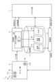
- FIG. 1 is a diagram showing an example of a schematic configuration of a semiconductor device according to an embodiment
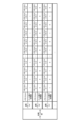
- FIG. 13 is a diagram illustrating an example of an initial pattern
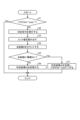
- 1A and 1B are diagrams illustrating an example of a process (time measurement method) executed in a semiconductor device.
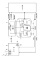
- FIG. 13 is a diagram showing an example of a schematic configuration of a semiconductor device according to a modified example.
- 1A and 1B are diagrams illustrating an example of a process (time measurement method) executed in a semiconductor device.
- FIG. 4 is a diagram illustrating an example of a circuit of a timer unit.
- FIG. 4 is a diagram illustrating an example of a circuit of a timer unit.
- FIG. 4 is a diagram illustrating an example of a circuit of a timer unit.
- the semiconductor device 1 is a diagram showing an example of a schematic configuration of a semiconductor device according to an embodiment of the present invention.
- the semiconductor device 1 includes a timer unit 2, a storage unit 4, a control unit 5, a determination unit 6, and a system unit 7.
- the timer unit 2 includes a plurality of memory cells 3.
- N memory cells 3 are exemplified as the plurality of memory cells 3. To distinguish between the memory cells 3, they are illustrated as memory cell 3-1, memory cell 3-2, memory cell 3-N, etc. When no particular distinction is made between them, they are simply referred to as memory cells 3.
- Each of the N memory cells 3 includes an MTJ element 30.
- the MTJ element 30 is a magnetic tunnel junction element. Examples of the MTJ element 30 include a spin transfer torque (STT) type MTJ element and a spin orbit torque (SOT) type MTJ element.
- STT spin transfer torque
- SOT spin orbit torque
- the resistance value of the MTJ element 30 changes between a low resistance value and a high resistance value.
- the memory cell 3 has a bit value of "1" or "0" depending on the resistance value of the MTJ element 30.
- a bit value is written to the memory cell 3 by setting the resistance value of the MTJ element 30 in the memory cell 3 to either a low resistance value or a high resistance value.
- the bit value written to the memory cell 3 can be read at any timing. Various known methods may be used for writing and reading.
- a memory cell 3 into which a bit value has been written will continue to maintain the same bit value for a certain amount of time (period), but after a longer period of time, the bit value may reverse from its original value (initial value). This phenomenon does not depend on whether the power supply to the semiconductor device 1 is on or off. In other words, regardless of whether there is a power supply or not, the bit value of the memory cell 3 may reverse from its initial value over time.
- the number of memory cells 3 whose bit values are inverted from the initial value is also referred to as the inversion number K.
- the time required for K memory cells 3 out of N memory cells 3 to be inverted is referred to as the timer time T.
- the timer time T depends on the retention characteristics of the MTJ element 30, and the retention characteristics are represented probabilistically by an exponential distribution.
- the average value of the timer time T (which can also be called an expected value, etc.) is referred to as the average value ⁇ T .
- the average value ⁇ T is expressed by the following formula (1).
- ⁇ can also be called a relaxation time or the like, and is determined by an index ⁇ of the thermal stability of the MTJ element 30. Specifically, ⁇ is expressed as in the following formula (2) using ⁇ and a constant ⁇ 0 .
- the number N of memory cells 3 can be designed and the number of inversions K can be set so that a desired average value ⁇ T can be obtained based on the thermal stability index ⁇ of the memory cells 3.
- the specific length of the average value ⁇ T is not particularly limited, but it can be, for example, one year, two years, or the like, or it can be shorter or longer.
- the memory unit 4 stores information used in the semiconductor device 1. Examples of information stored in the memory unit 4 include an initial pattern 41, a determination result 42, and a flag 43.
- the control unit 5 controls the timer unit 2.
- the control of the timer unit 2 by the control unit 5 includes initialization of the timer unit 2. Specifically, the control unit 5 writes an initial value to each of the N memory cells 3, thereby initializing the bit value of each of the N memory cells 3.
- control unit 5 initializes the timer unit 2 according to the initial pattern 41 stored in the memory unit 4.
- the initial pattern 41 describes the initial value of each bit value of the N memory cells 3. The explanation will be given with reference to FIG. 2 as well.
- FIG. 2 is a diagram showing examples of initial patterns.
- the initial pattern 41 describes, for each of the N memory cells 3, the memory cell 3 and the initial bit value in association with each other. Note that memory cell 3-N-5 in the diagram indicates the N-5th (N minus 5) memory cell 3. The same is true for memory cells 3-N-4 to 3-N-1.
- Three initial patterns are shown as examples in FIG. 2: initial pattern 41A, initial pattern 41B, and initial pattern 41C.
- Initial pattern 41A is a pattern that contains only the initial value "1". In initial pattern 41A, the initial values of all N memory cells 3 are "1".
- Initial pattern 41B is a pattern that includes only the initial value "0". In initial pattern 41B, the initial values of all N memory cells 3 are "0".
- Initial pattern 41C is a pattern that contains a mixture of initial values "1" and "0".
- the illustrated initial pattern 41C alternates between “1” and "0".
- the initial values "1" and “0” may be written so as to be mixed in various ways.
- an initial pattern 41 as described above is prepared in advance and stored in the memory unit 4.
- the control unit 5 initializes the timer unit 2 so that the bit value of each of the N memory cells 3 becomes the corresponding initial value in the initial pattern 41.
- the determination unit 6 determines the number of memory cells 3 whose bit values have been inverted from their initial values over time, that is, the inversion number K, out of the N memory cells 3.
- the determination unit 6 reads out the bit value of each of the N memory cells 3.
- the determination unit 6 counts the number of inversions K based on the result of comparing the bit value of each of the N memory cells 3 that have been read out with the corresponding initial value in the initial pattern 41.
- the determination unit 6 counts the number of memory cells 3 among the N memory cells 3 whose bit value is "0" as the inversion number K. Conversely, if all of the N memory cells 3 have an initial value of "0", the determination unit 6 counts the number of memory cells 3 among the N memory cells 3 whose bit value is "1" as the inversion number K.
- the function of the determination unit 6 may be realized by hardware such as a circuit, or by software.
- the determination unit 6 includes a count circuit 60 that counts the number of inversions K. Any circuit configuration capable of counting the number of inversions K may be adopted.
- the count circuit 60 includes an EXOR circuit that outputs the exclusive OR of the bit value of the read memory cell 3 and the corresponding initial value in the initial pattern 41. The total value of the exclusive OR of the bit values of each of the N memory cells 3 is counted as the number of inversions K.
- the determination of the number of inversions K by the determination unit 6 may be a threshold determination.
- the threshold set for the number of inversions K is referred to as the threshold Kth.
- the threshold Kth may be set to the same value as the number of inversions K determined by substituting a desired value for the average value ⁇ T in the above-mentioned formula (1).
- the determination unit 6 determines whether the inversion count K is greater than the threshold value Kth (whether K>Kth).
- the inversion count K being greater than the threshold value Kth indicates that the timer time T has elapsed since the initialization of the timer unit 2.
- the result of the judgment by the judgment unit 6 is stored in the memory unit 4 as the judgment result 42.
- the judgment result 42 includes information such as the bit value of each of the N memory cells 3 that were read, the number of inversions K that was counted, and whether or not the number of inversions K is greater than the threshold value Kth.
- Flag 43 may be updated according to judgment result 42.
- Flag 43 indicates whether or not the inversion count K is greater than threshold value Kth, i.e., whether or not timer time T has elapsed since initialization of timer unit 2.
- the specific configuration of the system unit 7 is not particularly limited, and it need only be designed to perform the above-mentioned operations.
- the design may be a hardware design, a software design, or a combination of hardware design and software design.
- the determination unit 6 determines the inversion number K, which is the number of memory cells 3 whose bit values have been inverted from their initial values over time, among the N memory cells 3. More specifically, the determination unit 6 determines whether the inversion number K is greater than a threshold value Kth.
- the fact that the inversion number K is greater than the threshold value Kth means that the timer time T has elapsed since the initialization of the timer unit 2. In other words, a time measurement function is provided.
- bit value may be inverted from the initial value over time, even if the power supply to the semiconductor device 1 is completely cut off. Therefore, the semiconductor device 1 can maintain the time measurement function regardless of the presence or absence of power.
- FIG. 3 is a diagram showing an example of processing (time measurement method) executed in a semiconductor device. Explanations of content that overlap with the above will be omitted as appropriate.
- the processing of this flowchart is executed when checking whether or not timer time T has elapsed since the initialization of timer section 2 of semiconductor device 1. There are no particular limitations on when the processing is executed, but the processing may be executed, for example, when the power supply of semiconductor device 1 is turned on.
- step S2 a judgment command is issued.
- the system unit 7 issues a judgment command to the judgment unit 6.
- step S3 the bit values are read.
- the determination unit 6 reads the bit values of each of the N memory cells 3.
- step S4 the number of inversions K is counted.
- the determination unit 6 counts the number of inversions K based on the result of comparing the bit values of each of the N memory cells 3 read in the previous step S3 with the corresponding initial values in the initial pattern 41.
- step S5 it is determined whether the number of inversions K is greater than the threshold value Kth.
- the determination unit 6 determines whether the number of inversions K counted in the previous step S4 is greater than the threshold value Kth. If the number of inversions K is greater than the threshold value Kth (step S5: Yes), processing proceeds to step S7. If not (step S5: No), processing proceeds to step S6.
- step S6 the judgment result 42 is stored.
- the judgment unit 6 stores the result of the judgment in the storage unit 4 as the judgment result 42.
- the judgment result 42 includes information such as the bit value of each of the N memory cells 3 that were read, the number of inversions K that was counted, and whether or not the number of inversions K is greater than the threshold value Kth.
- step S6 or step S7 After step S6 or step S7 is completed, the processing of the flowchart ends.
- the process of the above flowchart is called at any timing, and the above steps S1 to S7 are repeated the number of times it is called.
- the determination unit 6 repeatedly reads the bit values of each of the N memory cells 3, counts the number of inversions K, and determines whether the number of inversions K is greater than the threshold value Kth. When the number of inversions K becomes greater than the threshold value Kth and the flag 43 is activated, it indicates that the timer time T has elapsed since the initialization of the timer unit 2.
- FIG. 4 is a diagram showing an example of a schematic configuration of a semiconductor device according to a modified example.
- the judgment results 42 stored in the memory unit 4 include judgment results 42a and 42b.
- the judgment result 42a is the judgment result (current judgment result) obtained by the judgment unit 6 reading the current (latest) bit value.
- the judgment result 42a includes information such as the bit value of each of the N memory cells 3 read this time, the number of inversions K (the current number of inversions K), etc.
- the judgment result 42b is a judgment result (previous judgment result) obtained by the judgment unit 6 reading out past bit values, more specifically, by reading out the previous bit values.
- the judgment result 42b includes information such as the bit values of each of the N memory cells 3 previously read out, the number of inversions K (the previous number of inversions K), etc.
- the control unit 5 corrects the bit values of at least some of the N memory cells 3. This correction is also simply called the correction of the timer unit 2.
- the control unit 5 corrects the timer unit 2 so that the current reversal number K does not fall below the previous reversal number K. This makes it possible to eliminate (correct) the error of the reversal number K increasing over time.
- the determination unit 6 determines whether the current reversal number K is equal to or greater than the previous reversal number K. If this is not the case, i.e., if the current reversal number K is less than the previous reversal number K, the determination unit 6 sends a correction command to the control unit 5.
- the control unit 5 corrects the timer unit 2 in response to the correction command from the determination unit 6.
- the correction command may be sent to the control unit 5 from the system unit 7.
- the control unit 5 may correct the timer unit 2 by writing a value opposite to the initial value to the memory cell 3 to be corrected. For example, the control unit 5 writes a bit value of "0" to a memory cell 3 whose initial value is "1", or writes a bit value of "1" to a memory cell 3 whose initial value is "0".
- the control unit 5 may correct the timer unit 2 so that the bit value of each of the N memory cells 3 becomes the same as the bit value of each of the memory cells 3 that was previously read.
- the determination result 42b stored in the storage unit 4 may be referenced.
- the control unit 5 corrects the timer unit 2 so that the bit value of each of the N memory cells 3 becomes the corresponding bit value in the determination result 42b.
- the determination result 42a may be updated to reflect the correction result of the timer unit 2. Specifically, the determination result 42a is updated to include information such as the bit value of each of the N memory cells 3 after correction, the number of inversions K, etc. The update of the determination result 42a may be performed by the control unit 5 or by the determination unit 6.
- control unit 5 corrects the timer unit 2 as described above, it is possible to eliminate errors such as the inversion number K increasing over time. It is possible to suppress a decrease in the accuracy of time measurement that may occur due to an error.
- FIG. 5 is a diagram showing an example of the process (time measurement method) executed in a semiconductor device.
- the processes in steps S1 to S4 are as previously described with reference to FIG. 3. After the process in step S4 is completed, the process proceeds to step S11.
- step S11 it is determined whether the current reversal number K is equal to or greater than the previous reversal number K.
- the determination unit 6 determines whether the reversal number K counted in the previous step S4 (the current reversal number K) is equal to or greater than the reversal number K (the previous reversal number K) indicated in the determination result 42b stored in the memory unit 4. If the current reversal number K is equal to or greater than the previous reversal number K (step S11: Yes), processing proceeds to step S5. If not, i.e., if the current reversal number K is less than the previous reversal number K (step S11: No), processing proceeds to step S12.
- steps S5 to S7 is as previously described with reference to FIG. 3.
- step S12 the timer unit 2 is corrected.
- the determination unit 6 sends a correction command to the control unit 5.
- the control unit 5 corrects the timer unit 2.
- step S6 After step S6, step S7, or step S12 is completed, processing returns to step S2.
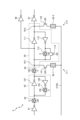
- 6 to 8 are diagrams showing examples of the timer circuit. Note that the specific operation of the circuit can be understood by those skilled in the art who have seen the circuit configurations shown in the drawings, so detailed explanations will be omitted.
- the timer unit 2 includes an NV-SRAM (non-volatile SRAM) circuit 8.
- the illustrated NV-SRAM circuit 8 is provided across two memory cells 3.
- the two memory cells 3 are illustrated as memory cells 3-1 and 3-2.
- the MTJ element 30 of memory cell 3-1 is illustrated as MTJ element 30-1.
- the MTJ element 30 of memory cell 3-2 is illustrated as MTJ element 30-2.
- NV-SRAM circuit 8 includes a latch circuit.
- the latch circuit is a flip-flop circuit, and its components are illustrated with reference numbers: transistor 81, inverter 82, inverter 83, and transistor 84.
- the transistors are assumed to be field effect transistors (FETs).
- FETs field effect transistors
- the drain and source of a transistor are also called current terminals. When an element is connected to the current terminal of a transistor, it is also simply said to be connected to the transistor.
- the gate of transistor 81 and the gate of transistor 84 are connected to the word line WL.
- Inverter 82 is connected between transistor 81 and transistor 84.
- Inverter 83 is connected in parallel to inverter 82 in the opposite direction to inverter 82.
- the connection point between transistor 81 and inverter 82 is called node N1 and illustrated.
- the connection point between inverter 82 and transistor 84 is called node N2 and illustrated.
- the control line CTRL is a voltage-controllable signal line. Between node N1 and the control line CTRL, a transistor 85 and an MTJ element 30-1 are connected in series. In addition, between node N2 and the control line CTRL, a transistor 86 and an MTJ element 30-2 are connected in series. A store/restore (write/read) signal SR is supplied to the gates of transistors 85 and 86.
- Bit values can be written and read by controlling the voltage level of the word line WL, the voltage level of the control line CTRL, and the store/restore signal SR, etc.
- a write current stores current
- a voltage corresponding to the resistance values of the MTJ elements 30-1 and 30-2 is detected.
- the timer unit 2 includes a NVDFF (non-volatile flip-flop) circuit 9.
- the illustrated NVDFF circuit 9 is provided across two memory cells 3, memory cell 3-1 and memory cell 3-2.
- the NVDFF circuit 9 includes a latch circuit.
- the latch circuit is a flip-flop circuit, and its components are illustrated with reference numbers: inverter 91, transmission gate 92, master latch 93, transmission gate 94, slave latch 95, inverter 96, and inverter 97.
- Master latch 93 includes inverter 101, inverter 102, and transmission gate 103.
- Inverter 102 and transmission gate 103 are connected in series, and they are connected in parallel to inverter 101 in the opposite direction to inverter 101.
- the slave latch 95 includes an inverter 111, an inverter 112, a transmission gate 113, and a transistor 114.
- the inverter 112 and the transmission gate 113 are connected in series, and they are connected in parallel to the inverter 111 in the opposite direction to the inverter 111.
- the transistor 114 is connected in parallel to the transmission gate 113.
- the slave latch 95 has a storage node N11 and a storage node N12.
- the storage node N11 is located on the input end side of the inverter 111.
- the storage node N12 is located on the output end side of the inverter 111.
- the input end of the inverter 96 is connected to the storage node N11.
- the input end of the inverter 97 is connected to the storage node N12.
- Transmission gate 92, transmission gate 94, transmission gate 103, and transmission gate 113 are supplied with clock signal C or its inverted signal, inverted clock signal CB.
- Transistor 121 and MTJ element 30-1 are connected in series between storage node N11 and control line CTRL.
- Transistor 122 and MTJ element 30-2 are connected in series between storage node N12 and control line CTRL.
- a store/restore signal SR is supplied to the gates of transistors 121 and 122.
- Bit values can be written and read by controlling the voltage level of the control line CTRL, the clock signal C, the inverted clock signal CB, and the store/restore signal SR.
- a write current stores current
- a voltage corresponding to the resistance values of the MTJ elements 30-1 and 30-2 is detected.
- an NV-SRAM circuit 8 or an NVDFF circuit 9 as described above is provided for two memory cells 3.
- the timer unit 2 may include multiple NV-SRAM circuits 8 or multiple NVDFF circuits 9, more specifically, N/2 NV-SRAM circuits 8 or N/2 NVDFF circuits 9.
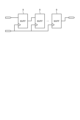
- the multiple NV-SRAM circuits 8 or multiple NVDFF circuits 9 may form a shift register.
- FIG. 8 shows an example of a shift register.
- multiple NVDFF circuits 9 are cascaded to form a shift register.
- the bit values of the memory cells 3 corresponding to each NVDFF circuit 9 are read out in sequence.
- the semiconductor device 1 described above may be mounted on an electronic device for use. Any electronic device can be the application target of the semiconductor device 1. By mounting the semiconductor device 1, a time measurement function is provided, and the time measurement function can be maintained regardless of the presence or absence of a power source.
- the semiconductor device 1 may be incorporated into a semiconductor memory device such as an NVSRAM or MRAM, or may be mounted in an electronic device together with such a semiconductor memory device. In this case, a part of the memory cell array of the semiconductor memory device may be used as the timer unit 2 of the semiconductor device 1.
- the semiconductor device 1 includes a plurality of memory cells 3 (N memory cells 3) each including an MTJ element 30 (magnetic tunnel junction element), and a determination unit 6 that determines an inversion number K, which is the number of memory cells 3 whose bit values have been inverted from their initial values over time, among the plurality of memory cells 3. For example, the determination unit 6 determines whether or not the inversion number K is greater than a threshold value Kth.
- the semiconductor device 1 includes a memory unit 4 that stores an initial pattern 41 that describes the initial value of each bit value of a plurality of memory cells 3, and the determination unit 6 may count the number of inversions K based on the result of comparing each bit value of the read out plurality of memory cells 3 with the corresponding initial value in the initial pattern 41.
- the initial pattern 41 may be an initial pattern 41A that includes only an initial value "1", an initial pattern 41B that includes only an initial value "0", or an initial pattern 41B that includes a mixture of initial values "1" and "0".
- the number of inversions K can be counted in this manner.
- the determination unit 6 may include a count circuit 60 that counts the number of inversions K.
- the number of inversions K can be counted by the function of the determination unit 6 realized by such hardware design.
- the function of the determination unit 6 may be software designed.
- the semiconductor device 1 may include a control unit 5 that initializes the bit values of each of the multiple memory cells 3 according to an initial pattern 41. By initializing the bit values of the multiple memory cells 3 according to a known pattern, it becomes possible to count the number of inversions K based on the comparison results in the determination unit 6 described above.
- the control unit 5 may correct the bit values of at least some of the memory cells 3.
- the determination unit 6 may repeatedly read out the bit values of the memory cells 3 and count the number of inversions K, and the control unit 5 may correct the bit values of at least some of the memory cells 3 so that the current number of inversions K is not lower than the previous number of inversions K.
- the control unit 5 may write a value opposite to the initial value to at least some of the memory cells 3.
- the control unit 5 may correct the bit values of at least some of the memory cells 3 so that the bit values of the memory cells 3 are the same as the bit values of the memory cells 3 previously read. By performing such a correction, it is possible to deal with an error in which the number of inversions K increases over time. It is possible to suppress a decrease in the accuracy of time measurement that may occur due to an error.
- the time measurement method described with reference to Figures 1 to 5 is also one of the disclosed technologies.
- the time measurement method includes determining an inversion number K, which is the number of memory cells 3 whose bit values have been inverted from their initial values over time, among a plurality of memory cells 3 each including an MTJ element 30 (steps S3 to S7). For example, the determination may involve determining whether or not the inversion number K is greater than a threshold value Kth (step S5).
- a time measurement method can also maintain the time measurement function regardless of the presence or absence of a power source.
- the determination may count the number of inversions K based on the comparison result between the bit value of each of the read memory cells 3 and the corresponding initial value in the initial pattern 41 that describes the initial value of each of the bit values of the multiple memory cells 3 (step S4).
- the initial pattern 41 may be an initial pattern 41A that includes only an initial value "1", an initial pattern 41B that includes only an initial value "0", or an initial pattern 41B that includes a mixture of initial values "1" and "0".
- the number of inversions K can be counted in this way.
- the count circuit 60 may count the number of inversions K by making the determination (step S4). For example, the number of inversions K can be counted in this manner.
- the time measurement method may include initializing the bit value of each of the plurality of memory cells 3 according to the initial pattern 41.
- initializing the bit values of the plurality of memory cells 3 according to a known pattern it becomes possible to count the number of inversions K based on the comparison result of the above-mentioned determination.
- the time measurement method may include correcting the bit values of at least some of the memory cells 3 (step S12).
- the determination may involve repeatedly reading out the bit values of each of the memory cells 3 and counting the number of inversions K (step S4, step S5: No, step S4 when the process of the flowchart is called next), and the correction may involve correcting the bit values of at least some of the memory cells 3 so that the current number of inversions K is not lower than the previous number of inversions K (step S11: No, step S12).
- the correction may involve writing a value opposite to the initial value to at least some of the memory cells 3 among the multiple memory cells 3 (step S12).
- the correction may involve correcting the bit values of at least some of the memory cells 3 among the multiple memory cells 3 so that the bit values of each of the multiple memory cells 3 are the same as the bit values of each of the multiple memory cells 3 read out previously (step S12).
- the present technology can also be configured as follows. (1) a plurality of memory cells each including a magnetic tunnel junction element; a determination unit that determines an inversion number, which is the number of memory cells whose bit values have been inverted from their initial values over time, among the plurality of memory cells; Equipped with Semiconductor device. (2) The determination unit determines whether the number of inversions is greater than a threshold value. A semiconductor device according to (1). (3) a memory unit that stores an initial pattern describing an initial value of each bit value of the plurality of memory cells; the determination unit counts the number of inversions based on a result of comparing the bit values of each of the plurality of memory cells read out with a corresponding initial value in the initial pattern; The semiconductor device according to (1) or (2).
- the initial pattern is A pattern that contains only the initial value "1", A pattern that contains only the initial value "0", Or, A pattern including a mixture of initial values "1" and "0".
- the determination unit includes a count circuit that counts the number of inversions.
- (6) a memory unit that stores an initial pattern describing an initial value of each bit value of the plurality of memory cells; a control unit that initializes a bit value of each of the plurality of memory cells according to the initial pattern; Equipped with A semiconductor device according to any one of (1) to (5).
- the determination unit repeatedly reads out the bit values of the plurality of memory cells and counts the number of inversions; the control unit corrects bit values of at least some of the memory cells among the plurality of memory cells so that the current number of inversions is not less than the previous number of inversions.
- the control unit writes a value opposite to an initial value into at least a portion of the memory cells among the plurality of memory cells;
- the control unit corrects bit values of at least some of the memory cells among the plurality of memory cells so that the bit values of the plurality of memory cells become the same as the bit values of the plurality of memory cells previously read.
- the determining step determines whether the number of inversions is greater than a threshold value.
- the number of inversions is counted based on a comparison result between the read bit value of each of the plurality of memory cells and a corresponding initial value in an initial pattern describing an initial value of each of the bit values of the plurality of memory cells.
- the initial pattern is A pattern that contains only the initial value "1", A pattern that contains only the initial value "0", Or, A pattern including a mixture of initial values "1" and "0".
- a counting circuit counts the number of inversions.
- the determining step includes repeatedly reading out the bit values of the plurality of memory cells and counting the number of inversions of the bit values of the plurality of memory cells; In the correction, the bit values of at least some of the memory cells are corrected so that the current number of inversions is not less than the previous number of inversions.
Landscapes
- Physics & Mathematics (AREA)
- General Physics & Mathematics (AREA)
- Static Random-Access Memory (AREA)
Abstract
半導体装置は、各々が磁気トンネル接合素子を含む複数のメモリセルと、複数のメモリセルのうち、時間経過によってビット値が初期値から反転したメモリセルの数である反転数を判定する判定部と、を備える。
Description
本開示は、半導体装置及び時間計測方法に関する。
例えば特許文献1には、時間計測機能を提供するためのRTC回路を備える半導体装置において、主電源がオフのときでもRTC回路に電力を供給して動作させるためのバックアップ電池を設ける技術が開示されている。
特許文献1の技術では、バックアップ電池が切れて電源が完全に遮断されると時間計測機能を維持できなくなる。
本開示の一側面は、電源の有無に関係なく時間計測機能を維持する。
本開示の一側面に係る半導体装置は、各々が磁気トンネル接合素子を含む複数のメモリセルと、複数のメモリセルのうち、時間経過によってビット値が初期値から反転したメモリセルの数である反転数を判定する判定部と、を備える。
本開示の一側面に係る時間計測方法は、各々が磁気トンネル接合素子を含む複数のメモリセルのうち、時間経過によってビット値が初期値から反転したメモリセルの数である反転数を判定すること、を含む。
以下に、本開示の実施形態について図面に基づいて詳細に説明する。なお、以下の実施形態において、同一の要素には同一の符号を付することにより重複する説明を省略する。
以下に示す項目順序に従って本開示を説明する。
1.実施形態
2.変形例
3.タイマー部の回路の例
4.適用例
5.まとめ
1.実施形態
2.変形例
3.タイマー部の回路の例
4.適用例
5.まとめ
1.実施形態
図1は、実施形態に係る半導体装置の概略構成の例を示す図である。半導体装置1は、タイマー部2と、記憶部4と、制御部5と、判定部6と、システム部7とを含む。
図1は、実施形態に係る半導体装置の概略構成の例を示す図である。半導体装置1は、タイマー部2と、記憶部4と、制御部5と、判定部6と、システム部7とを含む。
タイマー部2は、複数のメモリセル3を含む。複数のメモリセル3として、N個のメモリセル3が例示される。各メモリセル3を区別できるように、メモリセル3-1、メモリセル3-2、メモリセル3-N等と称し図示する。これらをとくに区別しない場合は、単にメモリセル3と呼ぶ。
N個のメモリセル3の各々は、MTJ素子30を含む。MTJ素子30は、磁気トンネル接合(Magnetic Tunnel Junction)素子である。MTJ素子30の例は、スピン注入磁化反転(STT:Spin Transfer Torque)型のMTJ素子、スピン軌道トルク(SOT:Spin Orbit Torque)型のMTJ素子等である。MTJ素子30の抵抗値は、低抵抗値と高抵抗値との間で変化する。
メモリセル3は、MTJ素子30の抵抗値に応じて、“1”又は“0”のビット値を有する。メモリセル3内のMTJ素子30の抵抗値を低抵抗値又は高抵抗値のいずれかにすることで、メモリセル3にビット値が書き込まれる。また、メモリセル3に書き込まれたビット値は、任意のタイミングで読み出される。書き込み及び読み出しには種々の公知の手法が用いられてよい。
ビット値が書き込まれたメモリセル3は、ある程度の時間(期間)は同じビット値を維持し続けるが、さらに長い時間が経過すると、そのビット値が当初の値(初期値)から反転し得る。この現象は、半導体装置1の電源のオン・オフに依存しない。すなわち、電源の有無に関係なく、時間経過によって、メモリセル3のビット値が初期値から反転し得る。
ビット値が初期値から反転したメモリセル3の数を、反転数Kとも称する。N個のメモリセル3のうち、K個のメモリセル3が反転するのに要する時間を、タイマー時間Tと称する。タイマー時間Tは、MTJ素子30の保持特性に依存し、その保持特性は指数分布で確率的に表される。タイマー時間Tの平均値(期待値等ともいえる)を、平均値μTと称する。平均値μTは、以下の式(1)で表される。

上記の式(1)中のτは、緩和時間等と呼ぶこともでき、MTJ素子30の熱安定性の指標Δによって決まる。具体的に、τは、Δ及び定数τ0を用いて、以下の式(2)のように表される。

メモリセル3の熱安定性の指標Δ等に基づいて、所望の平均値μTが得られるように、メモリセル3の数Nを設計したり、反転数Kを設定したりすることができる。平均値μTの具体的な長さはとくに限定されないが、例えば、1年、2年等であってもよいし、それよりも短くてもよく、また、それよりも長くてもよい。
記憶部4は、半導体装置1で用いられる情報を記憶する。記憶部4に記憶される情報として、初期パターン41、判定結果42及びフラグ43が例示される。
制御部5は、タイマー部2を制御する。制御部5によるタイマー部2の制御は、タイマー部2の初期化を含む。具体的に、制御部5は、N個のメモリセル3の各々に初期値を書き込むことにより、N個のメモリセル3の各々のビット値を初期化する。
図1に示される例では、制御部5は、記憶部4に記憶された初期パターン41に従って、タイマー部2を初期化する。初期パターン41は、N個のメモリセル3の各々のビット値の初期値を記述する。図2も参照して説明する。
図2は、初期パターンの例を示す図である。初期パターン41は、N個のメモリセル3の各々について、メモリセル3と、ビット値の初期値とを対応付けて記述する。なお、図中のメモリセル3-N-5は、N-5(Nマイナス5)番目のメモリセル3を示す。メモリセル3-N-4~メモリセル3-N-1についても同様である。図2には、初期パターン41A、初期パターン41B及び初期パターン41Cの3つの初期パターンが例示される。
初期パターン41Aは、初期値“1”だけを含むパターンである。初期パターン41Aでは、N個のメモリセル3のすべての初期値が“1”である。
初期パターン41Bは、初期値“0”だけを含むパターンである。初期パターン41Bでは、N個のメモリセル3のすべての初期値が“0”である。
初期パターン41Cは、初期値“1”及び初期値“0”を混在して含むパターンである。例示される初期パターン41Cは、“1”及び“0”を交互に記述する。これに限らず、初期値“1”及び初期値“0”がさまざまな態様で混在するようにそれらが記述されてよい。
図1に戻り、例えば上記のような初期パターン41が予め準備され、記憶部4に記憶される。制御部5は、N個のメモリセル3の各々のビット値が、初期パターン41中の対応する初期値になるように、タイマー部2を初期化する。各メモリセル3のビット値を既知のパターンに従って初期化することで、この後で説明する判定部6での比較が可能になる。
判定部6は、N個のメモリセル3のうち、時間経過によってビット値が初期値から反転したメモリセル3の数、すなわち反転数Kを判定する。
判定部6は、N個のメモリセル3の各々のビット値を読み出す。判定部6は、読み出したN個のメモリセル3の各々のビット値と、初期パターン41中の対応する初期値との比較結果に基づいて、反転数Kをカウントする。
例えば、N個のメモリセル3の初期値がいずれも“1”であれば、判定部6は、N個のメモリセル3のうち、ビット値が“0”になっているメモリセル3の数を、反転数Kとしてカウントする。反対に、N個のメモリセル3の初期値がいずれも“0”であれば、判定部6は、N個のメモリセル3のうち、ビット値が“1”になっているメモリセル3の数を、反転数Kとしてカウントする。
判定部6の機能は、回路等のハードウェアによって実現されてもよく、ソフトウェアによって実現されてもよい。図1に示される例では、判定部6は、反転数Kをカウントするカウント回路60を含む。反転数Kをカウントすることが可能なあらゆる回路構成が採用されてよい。一例として、カウント回路60は、読み出されたメモリセル3のビット値と、初期パターン41中の対応する初期値との排他的論理和を出力するEXOR回路等を含んで構成される。N個のメモリセル3の各々のビット値の排他的論理和の合計の値が、反転数Kとしてカウントされる。
判定部6による反転数Kの判定は、閾値判定であってよい。反転数Kに対して設定される閾値を、閾値Kthと称する。閾値Kthは、先に述べた式(1)において、平均値μTに所望の値を代入した場合に定まる反転数Kと同じ値に設定されてよい。
判定部6は、反転数Kが閾値Kthよりも大きいか否か(K>Kthであるか否か)を判定する。反転数Kが閾値Kthよりも大きいことは、タイマー部2の初期化時からタイマー時間Tが経過したことを示す。
判定部6による判定の結果は、判定結果42として記憶部4に記憶される。判定結果42は、読み出したN個のメモリセル3の各々のビット値、カウントした反転数K、反転数Kが閾値Kthよりも大きいか否か等の情報を含む。
判定結果42に応じて、フラグ43が更新され得る。フラグ43は、反転数Kが閾値Kthよりも大きいか否か、すなわちタイマー部2の初期化時からタイマー時間Tが経過したか否かを示す。フラグ43は、デフォルト状態では無効化されており(フラグ43=“Invalid”)、反転数Kが反転数K以下であることを示す。判定部6は、反転数Kが閾値Kthよりも大きいと判定すると、フラグ43を有効化する(フラグ43=“Valid”)。
システム部7は、制御部5を制御したり、判定部6を制御したりすることで、半導体装置1の全体を制御する。例えば、システム部7は、初期化命令を制御部5に送る。制御部5は、システム部7からの初期化命令に応じて、タイマー部2を初期化する。また、システム部7は、判定命令を判定部6に送る。判定部6は、システム部7からの判定命令に応じて、反転数Kを判定する。
また、システム部7は、判定部6の判定結果を取得する。この取得は、判定部6が判定結果をシステム部7に送ることによって行われてもよいし、システム部7が記憶部4に記憶された判定結果42を参照したり、フラグ43を参照したりすることによって行われてもよい。
システム部7の具体的な構成はとくに限定されず、上述の動作を行えるように設計されていればよい。設計は、ハードウェア設計であってもよいし、ソフトウェア設計であってもよいし、ハードウェア設計及びソフトウェア設計の組合せであってもよい。
以上で説明した半導体装置1によれば、判定部6が、N個のメモリセル3のうち、時間経過によってビット値が初期値から反転したメモリセル3の数である反転数Kを判定する。より具体的に、判定部6は、反転数Kが閾値Kthよりも大きいか否かを判定する。反転数Kが閾値Kthよりも大きいことは、タイマー部2の初期化時からタイマー時間Tが経過したことを意味する。すなわち、時間計測機能が提供される。
MTJ素子30を含むメモリセル3においては、例えば半導体装置1の電源が完全に遮断された場合でも、時間経過によってビット値が初期値から反転し得る。従って、半導体装置1によれば、電源の有無に関係なく時間計測機能を維持することができる。
図3は、半導体装置において実行される処理(時間計測方法)の例を示す図である。これまでと重複する内容については説明を適宜省略する。このフローチャートの処理は、半導体装置1のタイマー部2の初期化時からタイマー時間Tが経過したか否かを確認する際に実行される。処理の実行時期はとくに限定されないが、例えば半導体装置1の電源をオンにしたとき等に処理が実行されてよい。
ステップS1において、フラグ43が有効化されている(フラグ43=“Valid”)か否かが判定される。この処理は、例えばシステム部7によって実行される。フラグ43が有効化されている場合(ステップS1:Yes)、フローチャートの処理は終了する。先にも述べたように、有効化されたフラグ43はタイマー部2の初期化時からタイマー時間Tが経過していることを示し、従って時間計測機能が提供される。フラグ43が有効化されていない場合(ステップS1:No)、ステップS2に処理が進められる。
ステップS2において、判定命令が発行される。システム部7は、判定部6に対して判定命令を発行する。
ステップS3において、ビット値が読み出される。判定部6は、N個のメモリセル3の各々のビット値を読み出す。
ステップS4において、反転数Kがカウントされる。判定部6は、先のステップS3で読み出したN個のメモリセル3の各々のビット値と、初期パターン41中の対応する初期値との比較結果に基づいて、反転数Kをカウントする。
ステップS5において、反転数Kが閾値Kthよりも大きいか否かが判定される。判定部6は、先のステップS4でカウントした反転数Kが、閾値Kthよりも大きいか否かを判定する。反転数Kが閾値Kthよりも大きい場合(ステップS5:Yes)、ステップS7に処理が進められる。そうでない場合(ステップS5:No)、ステップS6に処理が進められる。
ステップS6において、判定結果42が記憶される。判定部6は、判定の結果を、判定結果42として記憶部4に記憶する。先にも述べたように、判定結果42は、読み出したN個のメモリセル3の各々のビット値、カウントした反転数K、反転数Kが閾値Kthよりも大きいか否か等の情報を含む。
ステップS7においては、判定結果42が記憶されるだけでなく、フラグ43が有効化される(フラグ43=“Valid”)。この処理は、判定部6によって実行される。
ステップS6又はステップS7の処理が完了した後は、フローチャートの処理は終了する。
上記のフローチャートの処理が任意のタイミングで呼び出され、呼び出された回数の分だけ、上記のステップS1~ステップS7の処理が繰り返し実行される。判定部6は、N個のメモリセル3の各々のビット値の読み出し、反転数Kのカウント、及び、反転数Kが閾値Kthよりも大きいか否かの判定等を繰り返し行う。反転数Kが閾値Kthよりも大きくなりフラグ43が有効化されると、タイマー部2の初期化時からタイマー時間Tが経過したことが示される。
2.変形例
反転数Kが時間経過によって増加するようなエラー(不整合)が生じることが考えられる。このようなエラーは、例えば、時間経過によってビット値が初期値から反転したメモリセル3のそのビット値が、何らかの理由でさらに反転した(初期値に戻った)場合等に生じ得る。エラーによって、時間計測の精度が低下し得る。この問題に対処するために、メモリセル3のビット値が補正されてよい。図4及び図5を参照して説明する。
反転数Kが時間経過によって増加するようなエラー(不整合)が生じることが考えられる。このようなエラーは、例えば、時間経過によってビット値が初期値から反転したメモリセル3のそのビット値が、何らかの理由でさらに反転した(初期値に戻った)場合等に生じ得る。エラーによって、時間計測の精度が低下し得る。この問題に対処するために、メモリセル3のビット値が補正されてよい。図4及び図5を参照して説明する。
図4は、変形例に係る半導体装置の概略構成の例を示す図である。記憶部4に記憶される判定結果42は、判定結果42a及び判定結果42bを含む。
判定結果42aは、判定部6による今回の(最新の)ビット値の読み出しによって得られた判定結果(今回の判定結果)である。例えば、判定結果42aは、今回読み出されたN個のメモリセル3の各々のビット値、反転数K(今回の反転数K)等の情報を含む。
判定結果42bは、判定部6による過去のビット値の読み出し、より具体的には前回のビット値の読み出しによって得られた判定結果(前回の判定結果)である。例えば、判定結果42bは、前回読み出されたN個のメモリセル3の各々のビット値、反転数K(前回の反転数K)等の情報を含む。
制御部5は、N個のメモリセル3のうちの少なくとも一部のメモリセル3のビット値を補正する。この補正のことを、単にタイマー部2の補正とも呼ぶ。
制御部5は、今回の反転数Kが前回の反転数Kを下回らないように、タイマー部2を補正する。これにより、反転数Kが時間経過によって増加するというエラーを解消(訂正)することができる。
例えば、判定部6は、今回の反転数Kが前回の反転数K以上であるか否かを判定する。該当しない場合、すなわち今回の反転数Kが前回の反転数Kを下回る場合、判定部6は、補正命令を制御部5に送る。制御部5は、判定部6からの補正命令に応じて、タイマー部2を補正する。なお、補正命令は、システム部7から制御部5に送られてもよい。
制御部5は、補正対象のメモリセル3に、初期値とは反対の値を書き込むことによってタイマー部2を補正してよい。例えば、制御部5は、初期値が“1”のメモリセル3に対してビット値“0”を書き込んだり、初期値が“0”のメモリセル3に対してビット値“1”を書き込んだりする。
制御部5は、N個のメモリセル3の各々のビット値が、前回読み出されたメモリセル3の各々のビット値と同じになるように、タイマー部2を補正してよい。記憶部4に記憶された判定結果42bが参照されてよい。制御部5は、N個のメモリセル3の各々のビット値が、判定結果42b中の対応するビット値になるように、タイマー部2を補正する。
タイマー部2の補正結果を反映するように、判定結果42aが更新されてよい。具体的に、補正後のN個のメモリセル3の各々のビット値、反転数K等の情報を含むように、判定結果42aが更新される。判定結果42aの更新は、制御部5によって行われてもよいし、判定部6によって行われてもよい。
上記のように制御部5がタイマー部2を補正することで、例えば反転数Kが時間経過によって増加するようなエラーを解消することができる。エラーに起因して生じ得る時間計測の精度の低下を抑制することができる。
図5は、半導体装置において実行される処理(時間計測方法)の例を示す図である。ステップS1~ステップS4の処理は、先に図3を参照して説明したとおりである。ステップS4の処理が完了した後、ステップS11に処理が進められる。
ステップS11において、今回の反転数Kが前回の反転数K以上であるか否かが判定される。判定部6は、先のステップS4でカウントした反転数K(今回の反転数K)が、記憶部4に記憶されている判定結果42bに示される反転数K(前回の反転数K)以上であるか否かを判定する。今回の反転数Kが前回の反転数K以上の場合(ステップS11:Yes)、ステップS5に処理が進められる。そうでない場合、すなわち今回の反転数Kが前回の反転数Kを下回る場合(ステップS11:No)、ステップS12に処理が進められる。
ステップS5~ステップS7の処理は、先に図3を参照して説明したとおりである。
ステップS12において、タイマー部2が補正される。判定部6は、補正命令を制御部5に送る。制御部5は、タイマー部2を補正する。
ステップS6、ステップS7又はステップS12の完了した後は、ステップS2に処理が戻される。
上記のようにタイマー部2を補正することで、例えば反転数Kが時間経過によって増加するようなエラーに起因して生じ得る時間計測の精度の低下を抑制することができる。
3.タイマー部の回路の例
図6~図8は、タイマー部の回路の例を示す図である。なお、具体的な回路の動作は、図示される回路構成に接した当業者であれば理解できるので、詳細な説明は省略する。
図6~図8は、タイマー部の回路の例を示す図である。なお、具体的な回路の動作は、図示される回路構成に接した当業者であれば理解できるので、詳細な説明は省略する。
図6に示される例では、タイマー部2は、NV-SRAM(不揮発性SRAM)回路8を含む。例示されるNV-SRAM回路8は、2つのメモリセル3にわたって設けられる。2つのメモリセル3として、メモリセル3-1及びメモリセル3-2が例示される。メモリセル3-1のMTJ素子30を、MTJ素子30-1と称し図示する。メモリセル3-2のMTJ素子30を、MTJ素子30-2と称し図示する。
NV-SRAM回路8は、ラッチ回路を含む。この例では、ラッチ回路は、フリップフロップ回路であり、その構成要素として、トランジスタ81、インバータ82、インバータ83及びトランジスタ84が符号を付して図示される。
トランジスタは、電界効果トランジスタ(FET)であるものとする。トランジスタのドレイン及びソースを、電流端子とも呼ぶ。ある要素がトランジスタの電流端子に接続されることを、単にトランジスタに接続されるともいう。
トランジスタ81のゲート及びトランジスタ84のゲートは、ワード線WLに接続される。インバータ82は、トランジスタ81とトランジスタ84との間に接続される。インバータ83は、インバータ82とは反対向きに、インバータ82に対して並列に接続される。トランジスタ81とインバータ82との接続点を、ノードN1と称し図示する。インバータ82とトランジスタ84との接続点を、ノードN2と称し図示する。
制御線CTRLは、電圧制御可能な信号線である。ノードN1と制御線CTRLとの間に、トランジスタ85及びMTJ素子30-1が直列に接続される。また、ノードN2と制御線CTRLとの間に、トランジスタ86及びMTJ素子30-2が直列に接続される。トランジスタ85のゲート及びトランジスタ86のゲートには、ストア/リストア(書き込み/読み出し)信号SRが供給される。
ワード線WLの電圧レベル、制御線CTRLの電圧レベル、及び、ストア/リストア信号SR等を制御することで、ビット値を書き込んだり読み出したりすることができる。ビット値を書き込む際は、MTJ素子30-1及びMTJ素子30-2の抵抗値が所望の抵抗値(低抵抗値又は高抵抗値)になるように、それらに書き込み電流(ストア電流)が流れる。ビット値を読み出す際は、MTJ素子30-1及びMTJ素子30-2が有する抵抗値に応じた電圧が検出される。具体的な動作及び原理は公知であるので説明は省略する。
図7に示される例では、タイマー部2は、NVDFF(不揮発性フリップフロップ)回路9を含む。例示されるNVDFF回路9は、メモリセル3-1及びメモリセル3-2の2つのメモリセル3にわたって設けられる。
NVDFF回路9は、ラッチ回路を含む。この例では、ラッチ回路は、フリップフロップ回路であり、その構成要素として、インバータ91、伝送ゲート92、マスターラッチ93、伝送ゲート94、スレーブラッチ95、インバータ96及びインバータ97が符号を付して図示される。
マスターラッチ93は、インバータ101、インバータ102及び伝送ゲート103を含む。インバータ102及び伝送ゲート103は直列に接続され、それらは、インバータ101とは反対向きに、インバータ101に対して並列に接続される。
スレーブラッチ95は、インバータ111、インバータ112、伝送ゲート113及びトランジスタ114を含む。インバータ112及び伝送ゲート113は直列に接続され、それらは、インバータ111とは反対向きに、インバータ111に対して並列に接続される。トランジスタ114は、伝送ゲート113に対して並列に接続される。
スレーブラッチ95は、記憶ノードN11及び記憶ノードN12を有する。記憶ノードN11は、インバータ111の入力端側に位置する。記憶ノードN12は、インバータ111の出力端側に位置する。記憶ノードN11に、インバータ96の入力端が接続される。記憶ノードN12に、インバータ97の入力端が接続される。
伝送ゲート92、伝送ゲート94、伝送ゲート103及び伝送ゲート113には、クロック信号C又はその反転信号である反転クロック信号CBが供給される。
記憶ノードN11と制御線CTRLとの間に、トランジスタ121及びMTJ素子30-1が直列に接続される。また、記憶ノードN12と制御線CTRLとの間に、トランジスタ122及びMTJ素子30-2が直列に接続される。トランジスタ121のゲート及びトランジスタ122のゲートには、ストア/リストア信号SRが供給される。
制御線CTRLの電圧レベル、クロック信号C、反転クロック信号CB、及び、ストア/リストア信号SR等を制御することで、ビット値を書き込んだり読み出したりすることができる。ビット値を書き込む際は、MTJ素子30-1及びMTJ素子30-2の抵抗値が所望の抵抗値(低抵抗値又は高抵抗値)になるように、それらに書き込み電流(ストア電流)が流れる。ビット値を読み出す際は、MTJ素子30-1及びMTJ素子30-2が有する抵抗値に応じた電圧が検出される。具体的な動作及び原理は公知であるので説明は省略する。
例えば上記のようなNV-SRAM回路8又はNVDFF回路9が、2つのメモリセル3に対して設けられる。タイマー部2は、複数のNV-SRAM回路8又は複数のNVDFF回路9、より具体的にはN/2個のNV-SRAM回路8又はN/2個のNVDFF回路9を含んでよい。一実施形態において、複数のNV-SRAM回路8又は複数のNVDFF回路9は、シフトレジスタを構成してよい。
図8には、シフトレジスタの例が示される。この例では、複数のNVDFF回路9がカスケード接続され、シフトレジスタを構成する。ビット値を読み出す際は、各NVDFF回路9に対応するメモリセル3のビット値が順に読み出される。
4.適用例
これまで説明した半導体装置1は、電子機器に搭載されて用いられてよい。あらゆる電子機器が半導体装置1の適用対象となり得る。半導体装置1が搭載されることで、時間計測機能が提供され、また、電源の有無に関係なく時間計測機能を維持することができる。
これまで説明した半導体装置1は、電子機器に搭載されて用いられてよい。あらゆる電子機器が半導体装置1の適用対象となり得る。半導体装置1が搭載されることで、時間計測機能が提供され、また、電源の有無に関係なく時間計測機能を維持することができる。
半導体装置1は、NVSRAM、MRAM等の半導体記憶装置に組み入れられてもよく、また、そのような半導体記憶装置と一緒に電子機器に搭載されてもよい。その場合、半導体記憶装置のメモリセルアレイの一部が、半導体装置1のタイマー部2として用いられてよい。
5.まとめ
以上で説明した技術は、例えば次のように特定される。開示される技術の1つは、半導体装置1である。図1~図5等を参照して説明したように、半導体装置1は、各々がMTJ素子30(磁気トンネル接合素子)を含む複数のメモリセル3(N個のメモリセル3)と、複数のメモリセル3のうち、時間経過によってビット値が初期値から反転したメモリセル3の数である反転数Kを判定する判定部6と、を備える。例えば、判定部6は、反転数Kが閾値Kthよりも大きいか否かを判定する。
以上で説明した技術は、例えば次のように特定される。開示される技術の1つは、半導体装置1である。図1~図5等を参照して説明したように、半導体装置1は、各々がMTJ素子30(磁気トンネル接合素子)を含む複数のメモリセル3(N個のメモリセル3)と、複数のメモリセル3のうち、時間経過によってビット値が初期値から反転したメモリセル3の数である反転数Kを判定する判定部6と、を備える。例えば、判定部6は、反転数Kが閾値Kthよりも大きいか否かを判定する。
上記の半導体装置1によれば、時間経過によってビット値が初期値から反転したメモリセル3の数である反転数Kが判定される。反転数Kの判定は、例えば反転数Kが閾値Kthよりも大きいか否かの判定であり、このことは、タイマー部2の初期化時からタイマー時間Tが経過したことを意味する。すなわち、時間計測機能が提供される。MTJ素子30を含むメモリセル3においては、例えば半導体装置1の電源が完全に遮断された場合でも、時間経過によってビット値が初期値から反転し得る。従って、電源の有無に関係なく時間計測機能を維持することができる。
図1及び図2等を参照して説明したように、半導体装置1は、複数のメモリセル3の各々のビット値の初期値を記述する初期パターン41を記憶する記憶部4を備え、判定部6は、読み出した複数のメモリセル3の各々のビット値と、初期パターン41中の対応する初期値との比較結果に基づいて、反転数Kをカウントしてよい。初期パターン41は、初期値“1”だけを含む初期パターン41A、初期値“0”だけを含む初期パターン41B、又は、初期値“1”及び初期値“0”を混在して含む初期パターン41Bであってよい。例えばこのようにして、反転数Kをカウントすることができる。
図1等を参照して説明したように、判定部6は、反転数Kをカウントするカウント回路60を含んでよい。例えばこのようなハードウェア設計によって実現された判定部6の機能により、反転数Kをカウントすることができる。なお、先にも述べたように、判定部6の機能はソフトウェア設計であってもよい。
図1等を参照して説明したように、半導体装置1は、初期パターン41に従って複数のメモリセル3の各々のビット値を初期化する制御部5を備えてよい。複数のメモリセル3のビット値を既知のパターンに従って初期化することで、上述の判定部6での比較結果に基づく反転数Kのカウントが可能になる。
図4及び図5等を参照して説明したように、制御部5は、複数のメモリセル3のうちの少なくとも一部のメモリセル3のビット値を補正してよい。例えば、判定部6は、複数のメモリセル3の各々のビット値の読み出し、及び、反転数Kのカウントを繰り返し行い、制御部5は、今回の反転数Kが前回の反転数Kを下回らないように、複数のメモリセル3のうちの少なくとも一部のメモリセルのビット値を補正してよい。制御部5は、複数のメモリセル3のうちの少なくとも一部のメモリセル3に、初期値とは反対の値を書き込んでよい。制御部5は、複数のメモリセル3の各々のビット値が、前回読み出された複数のメモリセル3の各々のビット値と同じになるように、複数のメモリセル3のうちの少なくとも一部のメモリセル3のビット値を補正してよい。このような補正を行うことにより、例えば反転数Kが時間経過によって増加するようなエラーに対処することができる。エラーに起因して生じ得る時間計測の精度の低下を抑制することができる。
図1~図5等を参照して説明した時間計測方法も、開示される技術の1つである。時間計測方法は、各々がMTJ素子30を含む複数のメモリセル3のうち、時間経過によってビット値が初期値から反転したメモリセル3の数である反転数Kを判定すること(ステップS3~ステップS7)、を含む。例えば、判定することでは、反転数Kが閾値Kthよりも大きいか否かを判定してよい(ステップS5)。このような時間計測方法によっても、これまで説明したように、電源の有無に関係なく時間計測機能を維持することができる。
図1~図3等を参照して説明したように、判定することでは、読み出した複数のメモリセル3の各々のビット値と、複数のメモリセル3の各々のビット値の初期値を記述する初期パターン41中の対応する初期値との比較結果に基づいて、反転数Kをカウントしてよい(ステップS4)。初期パターン41は、初期値“1”だけを含む初期パターン41A、初期値“0”だけを含む初期パターン41B、又は、初期値“1”及び初期値“0”を混在して含む初期パターン41Bであってよい。例えばこのようにして、反転数Kをカウントすることができる。
図1及び図3等を参照して説明したように、判定することでは、カウント回路60が反転数Kをカウントしてよい(ステップS4)。例えばこのようにして、反転数Kをカウントすることができる。
図1及び図3等を参照して説明したように、時間計測方法は、初期パターン41に従って、複数のメモリセル3の各々のビット値を初期化すること、を含んでよい。複数のメモリセル3のビット値を既知のパターンに従って初期化することで、上述の判定することでの比較結果に基づく反転数Kのカウントが可能になる。
図4及び図5等を参照して説明したように、時間計測方法は、複数のメモリセル3のうちの少なくとも一部のメモリセル3のビット値を補正すること(ステップS12)、を含んでよい。判定することでは、複数のメモリセル3の各々のビット値の読み出し、及び、反転数Kのカウントを繰り返し行い(ステップS4、ステップS5:No、次にフローチャートの処理が呼び出された場合のステップS4)、補正することでは、今回の反転数Kが前回の反転数Kを下回らないように、複数のメモリセル3のうちの少なくとも一部のメモリセル3のビット値を補正してよい(ステップS11:No、ステップS12)。補正することでは、複数のメモリセル3のうちの少なくとも一部のメモリセル3に、初期値とは反対の値を書き込んでよい(ステップS12)。補正することでは、複数のメモリセル3の各々のビット値が、前回読み出された複数のメモリセル3の各々のビット値と同じになるように、複数のメモリセル3のうちの少なくとも一部のメモリセル3のビット値を補正してよい(ステップS12)。このような補正を行うことにより、例えば反転数Kが時間経過によって増加するようなエラーに対処することができる。エラーに起因して生じ得る時間計測の精度の低下を抑制することができる。
なお、本開示に記載された効果は、あくまで例示であって、開示された内容に限定されない。他の効果があってもよい。
以上、本開示の実施形態について説明したが、本開示の技術的範囲は、上述の実施形態そのままに限定されるものではなく、本開示の要旨を逸脱しない範囲において種々の変更が可能である。また、異なる実施形態及び変形例にわたる構成要素を適宜組み合わせてもよい。
なお、本技術は以下のような構成も取ることができる。
(1)
各々が磁気トンネル接合素子を含む複数のメモリセルと、
前記複数のメモリセルのうち、時間経過によってビット値が初期値から反転したメモリセルの数である反転数を判定する判定部と、
を備える、
半導体装置。
(2)
前記判定部は、前記反転数が閾値よりも大きいか否かを判定する、
(1)に記載の半導体装置。
(3)
前記複数のメモリセルの各々のビット値の初期値を記述する初期パターンを記憶する記憶部を備え、
前記判定部は、読み出した前記複数のメモリセルの各々のビット値と、前記初期パターン中の対応する初期値との比較結果に基づいて、前記反転数をカウントする、
(1)又は(2)に記載の半導体装置。
(4)
前記初期パターンは、
初期値“1”だけを含むパターン、
初期値“0”だけを含むパターン、
又は、
初期値“1”及び初期値“0”を混在して含むパターン
である、
(3)に記載の半導体装置。
(5)
前記判定部は、前記反転数をカウントするカウント回路を含む、
(3)又は(4)に記載の半導体装置。
(6)
前記複数のメモリセルの各々のビット値の初期値を記述する初期パターンを記憶する記憶部と、
前記初期パターンに従って前記複数のメモリセルの各々のビット値を初期化する制御部と、
を備える、
(1)~(5)のいずれかに記載の半導体装置。
(7)
前記複数のメモリセルのうちの少なくとも一部のメモリセルのビット値を補正する制御部を備える、
(1)~(6)のいずれかに記載の半導体装置。
(8)
前記判定部は、前記複数のメモリセルの各々のビット値の読み出し、及び、反転数のカウントを繰り返し行い、
前記制御部は、今回の反転数が前回の反転数を下回らないように、前記複数のメモリセルのうちの少なくとも一部のメモリセルのビット値を補正する、
(7)に記載の半導体装置。
(9)
前記制御部は、前記複数のメモリセルのうちの少なくとも一部のメモリセルに、初期値とは反対の値を書き込む、
(7)又は(8)に記載の半導体装置。
(10)
前記制御部は、前記複数のメモリセルの各々のビット値が、前回読み出された前記複数のメモリセルの各々のビット値と同じになるように、前記複数のメモリセルのうちの少なくとも一部のメモリセルのビット値を補正する、
(7)~(9)のいずれかに記載の半導体装置。
(11)
各々が磁気トンネル接合素子を含む複数のメモリセルのうち、時間経過によってビット値が初期値から反転したメモリセルの数である反転数を判定すること、
を含む、
時間計測方法。
(12)
前記判定することでは、前記反転数が閾値よりも大きいか否かを判定する、
(11)に記載の時間計測方法。
(13)
前記判定することでは、読み出した前記複数のメモリセルの各々のビット値と、前記複数のメモリセルの各々のビット値の初期値を記述する初期パターン中の対応する初期値との比較結果に基づいて、前記反転数をカウントする、
(11)又は(12)に記載の時間計測方法。
(14)
前記初期パターンは、
初期値“1”だけを含むパターン、
初期値“0”だけを含むパターン、
又は、
初期値“1”及び初期値“0”を混在して含むパターン
である、
(13)に記載の時間計測方法。
(15)
前記判定することでは、カウント回路が前記反転数をカウントする、
(13)又は(14)に記載の時間計測方法。
(16)
前記複数のメモリセルの各々のビット値の初期値を記述する初期パターンに従って、前記複数のメモリセルの各々のビット値を初期化すること、
を含む、
(11)~(15)のいずれかに記載の時間計測方法。
(17)
前記複数のメモリセルのうちの少なくとも一部のメモリセルのビット値を補正すること、
を含む、
(11)~(16)のいずれかに記載の時間計測方法。
(18)
前記判定することでは、前記複数のメモリセルの各々のビット値の読み出し、及び、反転数のカウントを繰り返し行い、
前記補正することでは、今回の反転数が前回の反転数を下回らないように、前記複数のメモリセルのうちの少なくとも一部のメモリセルのビット値を補正する、
(17)に記載の時間計測方法。
(19)
前記補正することでは、前記複数のメモリセルのうちの少なくとも一部のメモリセルに、初期値とは反対の値を書き込む、
(17)又は(18)に記載の時間計測方法。
(20)
前記補正することでは、前記複数のメモリセルの各々のビット値が、前回読み出された前記複数のメモリセルの各々のビット値と同じになるように、前記複数のメモリセルのうちの少なくとも一部のメモリセルのビット値を補正する、
(17)~(19)のいずれかに記載の時間計測方法。
(1)
各々が磁気トンネル接合素子を含む複数のメモリセルと、
前記複数のメモリセルのうち、時間経過によってビット値が初期値から反転したメモリセルの数である反転数を判定する判定部と、
を備える、
半導体装置。
(2)
前記判定部は、前記反転数が閾値よりも大きいか否かを判定する、
(1)に記載の半導体装置。
(3)
前記複数のメモリセルの各々のビット値の初期値を記述する初期パターンを記憶する記憶部を備え、
前記判定部は、読み出した前記複数のメモリセルの各々のビット値と、前記初期パターン中の対応する初期値との比較結果に基づいて、前記反転数をカウントする、
(1)又は(2)に記載の半導体装置。
(4)
前記初期パターンは、
初期値“1”だけを含むパターン、
初期値“0”だけを含むパターン、
又は、
初期値“1”及び初期値“0”を混在して含むパターン
である、
(3)に記載の半導体装置。
(5)
前記判定部は、前記反転数をカウントするカウント回路を含む、
(3)又は(4)に記載の半導体装置。
(6)
前記複数のメモリセルの各々のビット値の初期値を記述する初期パターンを記憶する記憶部と、
前記初期パターンに従って前記複数のメモリセルの各々のビット値を初期化する制御部と、
を備える、
(1)~(5)のいずれかに記載の半導体装置。
(7)
前記複数のメモリセルのうちの少なくとも一部のメモリセルのビット値を補正する制御部を備える、
(1)~(6)のいずれかに記載の半導体装置。
(8)
前記判定部は、前記複数のメモリセルの各々のビット値の読み出し、及び、反転数のカウントを繰り返し行い、
前記制御部は、今回の反転数が前回の反転数を下回らないように、前記複数のメモリセルのうちの少なくとも一部のメモリセルのビット値を補正する、
(7)に記載の半導体装置。
(9)
前記制御部は、前記複数のメモリセルのうちの少なくとも一部のメモリセルに、初期値とは反対の値を書き込む、
(7)又は(8)に記載の半導体装置。
(10)
前記制御部は、前記複数のメモリセルの各々のビット値が、前回読み出された前記複数のメモリセルの各々のビット値と同じになるように、前記複数のメモリセルのうちの少なくとも一部のメモリセルのビット値を補正する、
(7)~(9)のいずれかに記載の半導体装置。
(11)
各々が磁気トンネル接合素子を含む複数のメモリセルのうち、時間経過によってビット値が初期値から反転したメモリセルの数である反転数を判定すること、
を含む、
時間計測方法。
(12)
前記判定することでは、前記反転数が閾値よりも大きいか否かを判定する、
(11)に記載の時間計測方法。
(13)
前記判定することでは、読み出した前記複数のメモリセルの各々のビット値と、前記複数のメモリセルの各々のビット値の初期値を記述する初期パターン中の対応する初期値との比較結果に基づいて、前記反転数をカウントする、
(11)又は(12)に記載の時間計測方法。
(14)
前記初期パターンは、
初期値“1”だけを含むパターン、
初期値“0”だけを含むパターン、
又は、
初期値“1”及び初期値“0”を混在して含むパターン
である、
(13)に記載の時間計測方法。
(15)
前記判定することでは、カウント回路が前記反転数をカウントする、
(13)又は(14)に記載の時間計測方法。
(16)
前記複数のメモリセルの各々のビット値の初期値を記述する初期パターンに従って、前記複数のメモリセルの各々のビット値を初期化すること、
を含む、
(11)~(15)のいずれかに記載の時間計測方法。
(17)
前記複数のメモリセルのうちの少なくとも一部のメモリセルのビット値を補正すること、
を含む、
(11)~(16)のいずれかに記載の時間計測方法。
(18)
前記判定することでは、前記複数のメモリセルの各々のビット値の読み出し、及び、反転数のカウントを繰り返し行い、
前記補正することでは、今回の反転数が前回の反転数を下回らないように、前記複数のメモリセルのうちの少なくとも一部のメモリセルのビット値を補正する、
(17)に記載の時間計測方法。
(19)
前記補正することでは、前記複数のメモリセルのうちの少なくとも一部のメモリセルに、初期値とは反対の値を書き込む、
(17)又は(18)に記載の時間計測方法。
(20)
前記補正することでは、前記複数のメモリセルの各々のビット値が、前回読み出された前記複数のメモリセルの各々のビット値と同じになるように、前記複数のメモリセルのうちの少なくとも一部のメモリセルのビット値を補正する、
(17)~(19)のいずれかに記載の時間計測方法。
1 半導体装置
2 タイマー部
3 メモリセル
3-1 メモリセル
3-2 メモリセル
30 MTJ素子
30-1 MTJ素子
30-2 MTJ素子
4 記憶部
41 初期パターン
41A 初期パターン
41B 初期パターン
41C 初期パターン
42 判定結果
42a 判定結果
42b 判定結果
43 フラグ
5 制御部
6 判定部
60 カウント回路
7 システム部
8 NV-SRAM回路
81 トランジスタ
82 インバータ
83 インバータ
84 トランジスタ
85 トランジスタ
86 トランジスタ
9 NVDFF回路
91 インバータ
92 伝送ゲート
93 マスターラッチ
94 伝送ゲート
95 スレーブラッチ
96 インバータ
97 インバータ
101 インバータ
102 インバータ
103 伝送ゲート
111 インバータ
112 インバータ
113 伝送ゲート
114 トランジスタ
121 トランジスタ
122 トランジスタ
C クロック信号
CB 反転クロック信号
CTRL 制御線
N1 ノード
N2 ノード
N11 記憶ノード
N12 記憶ノード
SR ストア/リストア信号
WL ワード線
2 タイマー部
3 メモリセル
3-1 メモリセル
3-2 メモリセル
30 MTJ素子
30-1 MTJ素子
30-2 MTJ素子
4 記憶部
41 初期パターン
41A 初期パターン
41B 初期パターン
41C 初期パターン
42 判定結果
42a 判定結果
42b 判定結果
43 フラグ
5 制御部
6 判定部
60 カウント回路
7 システム部
8 NV-SRAM回路
81 トランジスタ
82 インバータ
83 インバータ
84 トランジスタ
85 トランジスタ
86 トランジスタ
9 NVDFF回路
91 インバータ
92 伝送ゲート
93 マスターラッチ
94 伝送ゲート
95 スレーブラッチ
96 インバータ
97 インバータ
101 インバータ
102 インバータ
103 伝送ゲート
111 インバータ
112 インバータ
113 伝送ゲート
114 トランジスタ
121 トランジスタ
122 トランジスタ
C クロック信号
CB 反転クロック信号
CTRL 制御線
N1 ノード
N2 ノード
N11 記憶ノード
N12 記憶ノード
SR ストア/リストア信号
WL ワード線
Claims (20)
- 各々が磁気トンネル接合素子を含む複数のメモリセルと、
前記複数のメモリセルのうち、時間経過によってビット値が初期値から反転したメモリセルの数である反転数を判定する判定部と、
を備える、
半導体装置。 - 前記判定部は、前記反転数が閾値よりも大きいか否かを判定する、
請求項1に記載の半導体装置。 - 前記複数のメモリセルの各々のビット値の初期値を記述する初期パターンを記憶する記憶部を備え、
前記判定部は、読み出した前記複数のメモリセルの各々のビット値と、前記初期パターン中の対応する初期値との比較結果に基づいて、前記反転数をカウントする、
請求項1に記載の半導体装置。 - 前記初期パターンは、
初期値“1”だけを含むパターン、
初期値“0”だけを含むパターン、
又は、
初期値“1”及び初期値“0”を混在して含むパターン
である、
請求項3に記載の半導体装置。 - 前記判定部は、前記反転数をカウントするカウント回路を含む、
請求項3に記載の半導体装置。 - 前記複数のメモリセルの各々のビット値の初期値を記述する初期パターンを記憶する記憶部と、
前記初期パターンに従って前記複数のメモリセルの各々のビット値を初期化する制御部と、
を備える、
請求項1に記載の半導体装置。 - 前記複数のメモリセルのうちの少なくとも一部のメモリセルのビット値を補正する制御部を備える、
請求項1に記載の半導体装置。 - 前記判定部は、前記複数のメモリセルの各々のビット値の読み出し、及び、反転数のカウントを繰り返し行い、
前記制御部は、今回の反転数が前回の反転数を下回らないように、前記複数のメモリセルのうちの少なくとも一部のメモリセルのビット値を補正する、
請求項7に記載の半導体装置。 - 前記制御部は、前記複数のメモリセルのうちの少なくとも一部のメモリセルに、初期値とは反対の値を書き込む、
請求項7に記載の半導体装置。 - 前記制御部は、前記複数のメモリセルの各々のビット値が、前回読み出された前記複数のメモリセルの各々のビット値と同じになるように、前記複数のメモリセルのうちの少なくとも一部のメモリセルのビット値を補正する、
請求項7に記載の半導体装置。 - 各々が磁気トンネル接合素子を含む複数のメモリセルのうち、時間経過によってビット値が初期値から反転したメモリセルの数である反転数を判定すること、
を含む、
時間計測方法。 - 前記判定することでは、前記反転数が閾値よりも大きいか否かを判定する、
請求項11に記載の時間計測方法。 - 前記判定することでは、読み出した前記複数のメモリセルの各々のビット値と、前記複数のメモリセルの各々のビット値の初期値を記述する初期パターン中の対応する初期値との比較結果に基づいて、前記反転数をカウントする、
請求項11に記載の時間計測方法。 - 前記初期パターンは、
初期値“1”だけを含むパターン、
初期値“0”だけを含むパターン、
又は、
初期値“1”及び初期値“0”を混在して含むパターン
である、
請求項13に記載の時間計測方法。 - 前記判定することでは、カウント回路が前記反転数をカウントする、
請求項13に記載の時間計測方法。 - 前記複数のメモリセルの各々のビット値の初期値を記述する初期パターンに従って、前記複数のメモリセルの各々のビット値を初期化すること、
を含む、
請求項11に記載の時間計測方法。 - 前記複数のメモリセルのうちの少なくとも一部のメモリセルのビット値を補正すること、
を含む、
請求項11に記載の時間計測方法。 - 前記判定することでは、前記複数のメモリセルの各々のビット値の読み出し、及び、反転数のカウントを繰り返し行い、
前記補正することでは、今回の反転数が前回の反転数を下回らないように、前記複数のメモリセルのうちの少なくとも一部のメモリセルのビット値を補正する、
請求項17に記載の時間計測方法。 - 前記補正することでは、前記複数のメモリセルのうちの少なくとも一部のメモリセルに、初期値とは反対の値を書き込む、
請求項17に記載の時間計測方法。 - 前記補正することでは、前記複数のメモリセルの各々のビット値が、前回読み出された前記複数のメモリセルの各々のビット値と同じになるように、前記複数のメモリセルのうちの少なくとも一部のメモリセルのビット値を補正する、
請求項17に記載の時間計測方法。
Applications Claiming Priority (2)
| Application Number | Priority Date | Filing Date | Title |
|---|---|---|---|
| JP2023147640 | 2023-09-12 | ||
| JP2023-147640 | 2023-09-12 |
Publications (1)
| Publication Number | Publication Date |
|---|---|
| WO2025057727A1 true WO2025057727A1 (ja) | 2025-03-20 |
Family
ID=95022160
Family Applications (1)
| Application Number | Title | Priority Date | Filing Date |
|---|---|---|---|
| PCT/JP2024/030572 Pending WO2025057727A1 (ja) | 2023-09-12 | 2024-08-28 | 半導体装置及び時間計測方法 |
Country Status (1)
| Country | Link |
|---|---|
| WO (1) | WO2025057727A1 (ja) |
Cited By (1)
| Publication number | Priority date | Publication date | Assignee | Title |
|---|---|---|---|---|
| WO2025253914A1 (ja) * | 2024-06-05 | 2025-12-11 | ソニーセミコンダクタソリューションズ株式会社 | 検出回路及びセンサ装置 |
Citations (3)
| Publication number | Priority date | Publication date | Assignee | Title |
|---|---|---|---|---|
| JPS5382234A (en) * | 1976-12-28 | 1978-07-20 | Toshiba Corp | Sequence circuit with non-voltile storafe function |
| JPH0290309A (ja) * | 1988-09-28 | 1990-03-29 | Fujitsu Ltd | 実時間タイマレジスタ更新制御方式 |
| JP2003091987A (ja) * | 2001-09-18 | 2003-03-28 | Sony Corp | 磁気メモリ装置及びその記録制御方法 |
-
2024
- 2024-08-28 WO PCT/JP2024/030572 patent/WO2025057727A1/ja active Pending
Patent Citations (3)
| Publication number | Priority date | Publication date | Assignee | Title |
|---|---|---|---|---|
| JPS5382234A (en) * | 1976-12-28 | 1978-07-20 | Toshiba Corp | Sequence circuit with non-voltile storafe function |
| JPH0290309A (ja) * | 1988-09-28 | 1990-03-29 | Fujitsu Ltd | 実時間タイマレジスタ更新制御方式 |
| JP2003091987A (ja) * | 2001-09-18 | 2003-03-28 | Sony Corp | 磁気メモリ装置及びその記録制御方法 |
Non-Patent Citations (1)
| Title |
|---|
| KAMEI, AIKA: "A Variation-Aware MTJ Store Energy Estimation Model for Design Exploration of CGRA with Nonvolatile Flip-Flops", IPSJ SIG TECHNICAL REPORT, vol. 2022-ARC-248, no. 26, 4 March 2022 (2022-03-04), pages 1 - 7, XP009562188 * |
Cited By (1)
| Publication number | Priority date | Publication date | Assignee | Title |
|---|---|---|---|---|
| WO2025253914A1 (ja) * | 2024-06-05 | 2025-12-11 | ソニーセミコンダクタソリューションズ株式会社 | 検出回路及びセンサ装置 |
Similar Documents
| Publication | Publication Date | Title |
|---|---|---|
| TWI409640B (zh) | 記憶體系統 | |
| US10522222B2 (en) | Semiconductor device and error correction method | |
| US8194438B2 (en) | nvSRAM having variable magnetic resistors | |
| US10481965B2 (en) | Method and apparatus for determining status element total with sequentially coupled counting status circuits | |
| TWI790497B (zh) | 半導體記憶裝置 | |
| KR101666537B1 (ko) | 기억 회로 | |
| US11037643B2 (en) | Memory system for controlling magnetic memory | |
| TWI299870B (en) | Method and circuitry for identifying weak bits in an mram | |
| US20060007755A1 (en) | Nonvolatile memory device efficiently changing functions of field programmable gate array at high speed | |
| WO2025057727A1 (ja) | 半導体装置及び時間計測方法 | |
| US7170814B2 (en) | Multi-port semiconductor memory | |
| CN110222006B (zh) | 基于rram的处理器架构及控制方法 | |
| US8891326B1 (en) | Method of sensing data in magnetic random access memory with overlap of high and low resistance distributions | |
| WO2021075539A1 (ja) | 不揮発性記憶回路 | |
| EP3249654A2 (en) | Systems and methods for non-volatile flip flops | |
| JP7282749B2 (ja) | 不揮発性記憶回路 | |
| CN115410623A (zh) | 半导体装置 | |
| US7561485B2 (en) | Sense architecture | |
| TWI779715B (zh) | 半導體記憶裝置及其控制方法 | |
| US12494264B2 (en) | Memory device and error correction method thereof | |
| TWI908077B (zh) | 記憶體裝置及其錯誤修正方法 | |
| CN119296611A (zh) | 命令传输电路以及存储装置 | |
| US5687124A (en) | Circuit for identifying a memory cell having erroneous data stored therein | |
| JP2003007080A (ja) | ヒューズ回路ブロック |
Legal Events
| Date | Code | Title | Description |
|---|---|---|---|
| 121 | Ep: the epo has been informed by wipo that ep was designated in this application |
Ref document number: 24865230 Country of ref document: EP Kind code of ref document: A1 |