WO2025057592A1 - アンテナモジュール、および電子機器 - Google Patents
アンテナモジュール、および電子機器 Download PDFInfo
- Publication number
- WO2025057592A1 WO2025057592A1 PCT/JP2024/027072 JP2024027072W WO2025057592A1 WO 2025057592 A1 WO2025057592 A1 WO 2025057592A1 JP 2024027072 W JP2024027072 W JP 2024027072W WO 2025057592 A1 WO2025057592 A1 WO 2025057592A1
- Authority
- WO
- WIPO (PCT)
- Prior art keywords
- antenna
- circuit
- filter
- band
- radiating element
- Prior art date
- Legal status (The legal status is an assumption and is not a legal conclusion. Google has not performed a legal analysis and makes no representation as to the accuracy of the status listed.)
- Pending
Links
Images




Classifications
-
- H—ELECTRICITY
- H01—ELECTRIC ELEMENTS
- H01Q—ANTENNAS, i.e. RADIO AERIALS
- H01Q1/00—Details of, or arrangements associated with, antennas
- H01Q1/52—Means for reducing coupling between antennas; Means for reducing coupling between an antenna and another structure
-
- H—ELECTRICITY
- H01—ELECTRIC ELEMENTS
- H01Q—ANTENNAS, i.e. RADIO AERIALS
- H01Q5/00—Arrangements for simultaneous operation of antennas on two or more different wavebands, e.g. dual-band or multi-band arrangements
- H01Q5/30—Arrangements for providing operation on different wavebands
- H01Q5/378—Combination of fed elements with parasitic elements
Definitions
- This disclosure relates to an antenna module and electronic device that does not degrade radiation efficiency even when multiple antennas are placed in a small area.
- Patent Document 1 An antenna module equipped with multiple antennas to widen the available frequency band is disclosed in Japanese Patent No. 7176667 (Patent Document 1).
- this antenna module one of the multiple antennas is provided with a series resonant circuit, which is essentially grounded, thereby maintaining high radiation efficiency of one antenna without interference from the other antenna.
- Patent Document 1 Although there may be no interference in the high frequency range, one antenna can be considered to be GND from the other antenna, and the electromagnetic waves radiated from the other antenna will be absorbed by one antenna, which may degrade the radiation efficiency of the other antenna.
- This disclosure has been made to solve these problems, and its purpose is to provide an antenna module and electronic device that do not degrade radiation efficiency even when multiple antennas are placed in a small area.
- the antenna module includes a first antenna having a first resonant frequency, a second antenna having a second resonant frequency, and a first bandstop filter connected to the second antenna.
- the first antenna includes a first feed circuit and a first radiating element connected to the first feed circuit.
- the second antenna includes a second feed circuit and a second radiating element connected to the second feed circuit.
- the first bandstop filter blocks the first resonant frequency, and the first radiating element and the second radiating element are coupled in at least one of an electric field and a magnetic field, so that a first path from ground through the first bandstop filter and the second radiating element operates as a non-powered antenna having a third resonant frequency.
- the electronic device includes the antenna module described above and a substrate on which the antenna module is mounted.
- the first band-stop filter blocks the first resonant frequency
- the first radiating element and the second radiating element are coupled in at least one of an electric field and a magnetic field, so that the first path from ground through the first band-stop filter and the second radiating element operates as a parasitic antenna having a third resonant frequency, and therefore radiation efficiency is not degraded even when multiple antennas are placed in a small area.
- FIG. 1 is a diagram showing a configuration of an antenna module according to a first embodiment
- FIG. 2 is a diagram showing a circuit diagram of a band-stop filter in the antenna module according to the first embodiment.
- FIG. 13 is a circuit diagram of a band-stop filter in a modified example.
- FIG. 13 is a diagram showing a circuit diagram of a band-stop filter in an antenna module according to another modified example.
- FIG. 11 is a diagram illustrating an example of the characteristics of a band-stop filter.
- 13 is a diagram showing a configuration of an antenna module in which a reactor is provided in a first path.
- FIG. 5 is a diagram showing an example of radiation efficiency of the first antenna in the first embodiment.
- FIG. 5 is a diagram showing an example of radiation efficiency of a second antenna in the first embodiment.
- FIG. 1 is a diagram showing a configuration of an electronic device in a first embodiment.
- 13 is a diagram showing a configuration of an antenna module in a modified example of the first embodiment.
- FIG. 13 is a diagram showing a configuration of a modified example of a band-stop filter.
- 13 is a diagram showing a configuration of an antenna module in a second embodiment.
- the radiation efficiency in this disclosure indicates the ratio of the output radiated from the antenna to the power supplied from the power feed circuit. In other words, it is the efficiency including losses in the circuit and losses due to matching mismatch with respect to the power supplied from the power feed circuit, and the smaller the negative value at the top of the graph, the better the radiation efficiency.
- the antenna module 1 includes a first antenna 100, a second antenna 200, and a band-stop filter 10 (first band-stop filter) connected to the second antenna 200.
- the first antenna 100 includes a feed circuit RF1 (first feed circuit) and a first radiating element 101.
- the second antenna 200 includes a feed circuit RF2 (second feed circuit) and a second radiating element 201.
- the antenna module 1 is mounted on, for example, a mobile terminal such as a mobile phone, smartphone, or tablet, or a communication device such as a smart watch or personal computer with a communication function.
- the first antenna 100 is, for example, a monopole antenna.
- the second antenna 200 is, for example, a monopole antenna.
- the power supply circuit RF1 supplies a high-frequency signal in the f1 frequency band (first resonant frequency) to the first radiating element 101.
- the first radiating element 101 can radiate the f1 frequency signal supplied from the power supply circuit RF1 into the air as radio waves.
- the f1 frequency band is, for example, a band that includes n77 (3.3-4.2 GHz).
- the power supply circuit RF2 supplies a high-frequency signal in the f2 frequency band (second resonant frequency) to the second radiating element 201.
- the second radiating element 201 can radiate the high-frequency signal in the f2 frequency band supplied from the power supply circuit RF2 into the air as radio waves.
- the f2 frequency band is, for example, a band that includes the WiFi (registered trademark) 5 GHz band.
- a band-stop filter 10 is connected between the second radiating element 201 and ground.
- the band-stop filter 10 blocks or attenuates high-frequency signals in the f1 frequency band.
- the band-stop filter 10 is configured to pass high-frequency signals in the f2 frequency band.
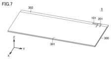
- the first radiating element 101 and the second radiating element 201 are mounted on the same board, as described below.
- the first radiating element 101 and the second radiating element 201 are provided on the same board, but they may be provided on different boards as long as they are provided within the same antenna module 1. By providing them on the same board in this way, the distance between the antennas is constant, so the coupling state between the first radiating element 101 and the second radiating element 201 can always be kept constant.
- the first radiating element 101 and the second radiating element 201 are coupled by at least one of an electric field and a magnetic field.
- the band-stop filter 10 is disposed between the second radiating element 201 and the ground.
- the path from the ground through the band-stop filter 10 and the second radiating element 201 functions as a parasitic antenna in the f3 frequency band (third resonant frequency).
- the f3 frequency band (third resonant frequency) may be the same communication band as the f1 frequency band (first resonant frequency).
- FIG. 2A is a diagram showing a circuit diagram of the bandstop filter 10 in the antenna module 1 in the first embodiment.
- the bandstop filter 10 includes a first filter circuit connected between the ground and the second radiating element 201 and resonating in series, and a second filter circuit connected to the second radiating element 201 and resonating in parallel.
- a second capacitor C2 and a second coil L2 are connected in parallel between the second radiating element 201 and the power feed circuit RF2.
- a first capacitor C1 and a first coil L1 are connected in series between one end of the second filter circuit and the ground.
- the second filter circuit is connected closer to the power feed circuit RF2 than the first filter circuit.
- the bandstop filter 10 is configured to block or attenuate high-frequency signals in the f1 frequency band and pass high-frequency signals in the f2 frequency band.
- Figure 3 is a diagram showing an example of the characteristics of the bandstop filter 10.
- the horizontal axis of Figure 3 is frequency [GHz]
- the vertical axis on the right side is return loss (S11) [dB]
- the vertical axis on the left side is insertion loss (S21) [dB].
- the solid line indicates return loss and the dashed line indicates insertion loss
- the characteristics of the bandstop filter 10 are high return loss (S11) and low insertion loss (S21) at frequencies of 3.3-4.2 GHz.
- the antenna module 1 provides the second antenna 200 with a band-stop filter 10 that blocks or attenuates high-frequency signals in the f1 band frequency band, thereby blocking or attenuating the passage of high-frequency signals in the f1 band frequency band from the first antenna 100, thereby maintaining a high radiation efficiency of the first antenna 100. Furthermore, the antenna module 1 operates as a parasitic antenna with a frequency band of f3 band through the first path T1 shown in FIG. 2A, which runs from the ground through the band-stop filter 10 to the second radiating element 201.
- the electromagnetic waves radiated from the first antenna 100 are not absorbed by the second antenna 200, and deterioration of the radiation efficiency of the first antenna 100 can be suppressed.
- the band-stop filter 10 By using the band-stop filter 10 in this way, the radiation efficiency can be maintained even when the two antennas are placed close to each other.
- the first path T1 In order for the first path T1 to operate as a parasitic antenna having a frequency band of the f3 band, for example, the first path T1 is made to resonate at 1/4 wavelength of the f3 band frequency band.
- the first path T1 includes a first filter circuit (first capacitor C1 and first coil L1), but if it does not resonate at 1/4 wavelength of the f3 band frequency band, it may be adjusted by providing at least one element of a reactor and a capacitor.
- FIG. 2B is a diagram showing a circuit diagram of a bandstop filter in the modified example.
- the bandstop filter 10 shown in FIG. 2B includes a first filter circuit connected between the ground and the second radiating element 201, in which a series resonant circuit and an inductor circuit are connected in parallel, and a second filter circuit connected to the second radiating element 201 and resonating in parallel.
- the first filter circuit includes a series resonant circuit in which a first capacitor C1 and a first coil L1 are connected in series between one end of the second filter circuit and the ground, and an inductor circuit including a third coil L3, which are connected in parallel.
- the first filter circuit shown in FIG. 2B can reduce the signal of the second resonant frequency flowing to ground while maintaining the pass characteristics of the third resonant frequency, thereby improving the radiation efficiency of the second resonant frequency.
- FIG. 2C is a diagram showing a circuit diagram of a bandstop filter in another modified example.
- the bandstop filter 10 shown in FIG. 2C includes a first filter circuit connected between the ground and the second radiating element 201, in which a series resonant circuit and a capacitance circuit are connected in parallel, and a second filter circuit connected to the second radiating element 201 and resonating in parallel.
- the first filter circuit includes a series resonant circuit in which a first capacitor C1 and a first coil L1 are connected in series between one end of the second filter circuit and the ground, and a capacitance circuit including a third capacitor C3, which are connected in parallel.
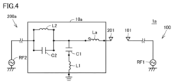
- FIG. 4 is a diagram showing the configuration of an antenna module 1a in which an inductor is provided in the first path T1.
- a coil La is provided so that the first path T1 of the bandstop filter 10a provided in the first antenna 100a resonates at 1/4 wavelength of the f3 frequency band.
- the coil La is provided between the first filter circuit and the second radiating element 201.
- the bandstop filter 10a may be provided with at least one of an inductor and a capacitor so that the first path T1 resonates at 1/4 wavelength of the f3 frequency band.
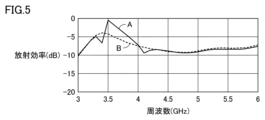
- FIG. 5 is a diagram showing an example of the radiation efficiency of the first antenna 100 in the first embodiment.
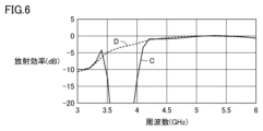
- FIG. 6 is a diagram showing an example of the radiation efficiency of the second antenna 200 in the first embodiment.
- the horizontal axis is frequency [GHz]
- the vertical axis is radiation efficiency [dB].
- the radiation efficiency of the first antenna 100 and the second antenna 200 in the first embodiment is shown by solid waveforms A and C
- the radiation efficiency of the first antenna 100 and the second antenna 200 without the band-stop filter 10 is shown by dashed waveforms B and D.
- the radiation efficiency of the solid line waveform A is higher than the radiation efficiency of the dashed line waveform B. Therefore, it can be seen that the radiation efficiency of the first antenna 100 of the antenna module 1 is improved by providing the bandstop filter 10.
- the radiation efficiency of the solid waveform C is not degraded, just like the radiation efficiency of the dashed waveform D.
- the second antenna 200 of the antenna module 1 blocks the band including n77 (3.3-4.2 GHz) by providing the bandstop filter 10.
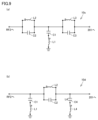
- FIG. 9 is a diagram showing the configuration of a modified example of a bandstop filter.
- Bandstop filter 10c shown in Figure 9(a) is configured with a three-stage filter circuit in which a third filter circuit that resonates in parallel with the first filter circuit and the second filter circuit is added.
- a third capacitor C3 and a third coil L3 are connected in parallel to the second radiating element 201.
- Fig. 10 is a diagram showing a configuration of an antenna module 2 in embodiment 2.
- the same components as those in the antenna module 1 shown in Fig. 2A are denoted by the same reference characters and detailed description thereof will not be repeated.
- the antenna module 2 includes a first antenna 100a, a second antenna 200, a bandstop filter 10 (first bandstop filter) connected to the second antenna 200, and a bandstop filter 20 (second bandstop filter) connected to the first antenna 100a.
- the first antenna 100a includes a power feed circuit RF1 (first power feed circuit) and a first radiating element 101.
- the second antenna 200 includes a power feed circuit RF2 (second power feed circuit) and a second radiating element 201.
- a band-stop filter 20 is connected to the first radiating element 101, and the band-stop filter 20 is also connected to ground.
- the band-stop filter 20 passes high-frequency signals in the f1 frequency band.
- the band-stop filter 20 is configured to block or attenuate high-frequency signals in the f2 frequency band.
- a band-stop filter 10 is connected between the second radiating element 201 and ground.
- the band-stop filter 10 blocks or attenuates high-frequency signals in the f1 frequency band.
- the band-stop filter 10 is configured to pass high-frequency signals in the f2 frequency band.
- the bandstop filter 20 includes a fifth filter circuit that is connected between ground and the first radiating element 101 and resonates in series, and a sixth filter circuit that is connected to the first radiating element 101 and resonates in parallel.
- a capacitor CA and a coil LA are connected in series between the first radiating element 101 and ground.
- a capacitor CB and a coil LB are connected in parallel between the first radiating element 101 and the power feed circuit RF1.
- the sixth filter circuit is arranged on the power feed circuit RF1 side
- the fifth filter circuit is arranged on the first radiating element 101 side.
- the antenna module 2 operates as a parasitic antenna with a frequency band of f4 (fourth resonant frequency) on the second path T2 that runs from the ground of the first antenna 100a through the bandstop filter 20 and the first radiating element 101.
- f4 fourth resonant frequency
- the second path T2 In order for the second path T2 to operate as a parasitic antenna having a frequency band of f4, for example, the second path T2 is set to resonate at 1/4 wavelength of the f4 frequency band.
- the second path T2 includes a fifth filter circuit (capacitor CA and coil LA), but if it does not resonate at 1/4 wavelength of the f4 frequency band, it may be adjusted by providing at least one element of a reactor and a capacitor.
- the circuit configuration of the bandstop filter 20 may be that of the bandstop filter 10b shown in FIG. 8, the bandstop filter 10c shown in FIG. 9(a), or the bandstop filter 10d shown in FIG. 9(b).
- the frequency band of the f4 band may be the same as the frequency band of the f2 band, or a different frequency band.
- the frequency band of the f4 band is the same as the frequency band of the f2 band, the radiation of the first antenna 100a is added to the second antenna 200, improving the radiation efficiency.
- the frequency band of the f4 band is different from the frequency band of the f2 band, resonance of a frequency band different from the frequency band of the f2 band is added to the second antenna 200, enabling a wider band.
- the antenna device is described as a monopole antenna, but the antenna device may be another type of antenna, such as an inverted F antenna.
- the antenna module includes: a first antenna having a first resonant frequency; a second antenna having a second resonant frequency; a first band-stop filter connected to the second antenna;
- the first antenna includes a first feeding circuit and a first radiating element connected to the first feeding circuit;
- the second antenna includes a second feeding circuit and a second radiating element connected to the second feeding circuit;
- the first band-stop filter blocks a first resonant frequency;
- the antenna module according to (1) The first path resonates at a quarter wavelength of the third resonant frequency and operates as a parasitic antenna having the third resonant frequency.
- the antenna module according to (2), The first path includes at least one of a reactor and a capacitor for resonating at a quarter wavelength of the third resonant frequency.
- the antenna module according to any one of (1) to (4),
- the first band-stop filter is a first filter circuit connected between the ground and the second radiating element and resonating in series; and a second filter circuit connected between the second radiating element and the feed circuit and resonating in parallel.
- the antenna module according to any one of (1) to (4),
- the first band-stop filter is a first filter circuit connected between the ground and the second radiating element, the first filter circuit including a series resonant circuit and an inductor circuit connected in parallel; and a second filter circuit connected between the second radiating element and the feed circuit and resonating in parallel.
- the antenna module is a first filter circuit connected between the ground and the second radiating element, the first filter circuit including a series resonant circuit and a capacitance circuit connected in parallel; and a second filter circuit connected between the second radiating element and the feed circuit and resonating in parallel.
- the antenna module according to any one of (5) to (7),
- the first band-stop filter is connected such that the second filter circuit is closer to the second feed circuit than the first filter circuit.
- the antenna module according to any one of (5) to (7),
- the first band-stop filter is connected such that the first filter circuit is closer to the second feed circuit than the second filter circuit.
- the antenna module according to any one of (5) to (9),
- the first band-stop filter further includes at least one of a series-resonating filter circuit and a parallel-resonating filter circuit in the first filter circuit and the second filter circuit.
- the antenna module according to any one of (1) to (10), a second bandstop filter coupled to the first antenna; The second bandstop filter blocks a fourth resonant frequency.
- the antenna module according to (11) or (12), The fourth resonant frequency is in the same communication band as the second resonant frequency.
- An electronic device according to the present disclosure, The antenna module according to any one of (1) to (13), and a substrate on which the antenna module is mounted.
Landscapes
- Details Of Aerials (AREA)
- Variable-Direction Aerials And Aerial Arrays (AREA)
Priority Applications (2)
| Application Number | Priority Date | Filing Date | Title |
|---|---|---|---|
| JP2025545521A JPWO2025057592A1 (https=) | 2023-09-13 | 2024-07-30 | |
| CN202480049494.4A CN121586971A (zh) | 2023-09-13 | 2024-07-30 | 天线模块和电子设备 |
Applications Claiming Priority (2)
| Application Number | Priority Date | Filing Date | Title |
|---|---|---|---|
| JP2023148309 | 2023-09-13 | ||
| JP2023-148309 | 2023-09-13 |
Publications (1)
| Publication Number | Publication Date |
|---|---|
| WO2025057592A1 true WO2025057592A1 (ja) | 2025-03-20 |
Family
ID=95022049
Family Applications (1)
| Application Number | Title | Priority Date | Filing Date |
|---|---|---|---|
| PCT/JP2024/027072 Pending WO2025057592A1 (ja) | 2023-09-13 | 2024-07-30 | アンテナモジュール、および電子機器 |
Country Status (3)
| Country | Link |
|---|---|
| JP (1) | JPWO2025057592A1 (https=) |
| CN (1) | CN121586971A (https=) |
| WO (1) | WO2025057592A1 (https=) |
Citations (2)
| Publication number | Priority date | Publication date | Assignee | Title |
|---|---|---|---|---|
| JP7176667B2 (ja) * | 2020-07-20 | 2022-11-22 | 株式会社村田製作所 | アンテナ装置、アンテナシステム及び通信端末装置 |
| WO2023120075A1 (ja) * | 2021-12-22 | 2023-06-29 | 株式会社村田製作所 | アンテナモジュール |
-
2024
- 2024-07-30 WO PCT/JP2024/027072 patent/WO2025057592A1/ja active Pending
- 2024-07-30 CN CN202480049494.4A patent/CN121586971A/zh active Pending
- 2024-07-30 JP JP2025545521A patent/JPWO2025057592A1/ja active Pending
Patent Citations (2)
| Publication number | Priority date | Publication date | Assignee | Title |
|---|---|---|---|---|
| JP7176667B2 (ja) * | 2020-07-20 | 2022-11-22 | 株式会社村田製作所 | アンテナ装置、アンテナシステム及び通信端末装置 |
| WO2023120075A1 (ja) * | 2021-12-22 | 2023-06-29 | 株式会社村田製作所 | アンテナモジュール |
Non-Patent Citations (1)
| Title |
|---|
| 小西 良弘 他, 通信用フィルタ回路の設計とその応用, 第2版, 総合電子出版社, 05 April 1997, non-official translation (KONISHI, Yoshihiro et al., Design of communication filter circuit and its application, 2nd edition, SOGO DENSHI SHUPPANSHA) pp. 11-15, 24-28, 49-51, fig. 2.23, 2.43 * |
Also Published As
| Publication number | Publication date |
|---|---|
| JPWO2025057592A1 (https=) | 2025-03-20 |
| CN121586971A (zh) | 2026-02-27 |
Similar Documents
| Publication | Publication Date | Title |
|---|---|---|
| CN114258612B (zh) | 天线及电子设备 | |
| CN107959117B (zh) | 用于减少天线间互耦的天线组件和自愈式的去耦合方法 | |
| JP4017852B2 (ja) | 小型マイクロ波アンテナ | |
| TWI425713B (zh) | 諧振產生之三頻段天線 | |
| JP6282653B2 (ja) | 印刷回路基板アンテナ及び端末 | |
| EP1553659B1 (en) | Small multimode antenna and high frequency module using it | |
| US10263336B1 (en) | Multi-band multi-antenna array | |
| WO2014098024A1 (ja) | アンテナ装置および電子機器 | |
| JPH11136025A (ja) | 周波数切換型表面実装型アンテナおよびそれを用いたアンテナ装置およびそれを用いた通信機 | |
| US9258019B2 (en) | Communication device | |
| US7999746B2 (en) | Printed circuit board having built-in antenna | |
| US7982682B2 (en) | Antenna apparatus | |
| KR20100042704A (ko) | 미모 안테나 장치 | |
| JPWO2020137375A1 (ja) | アンテナ装置 | |
| US20240347903A1 (en) | Antenna Structure and Electronic Device | |
| US20190252786A1 (en) | Devices and methods for implementing mimo in metal ring structures using tunable electrically small antennas | |
| US20240235516A1 (en) | Filter device, antenna device, and antenna module | |
| US12494760B2 (en) | Filter device, antenna device, and antenna module | |
| JP7582516B2 (ja) | アンテナモジュール | |
| KR101554695B1 (ko) | 통신 단말 장치 | |
| WO2025057592A1 (ja) | アンテナモジュール、および電子機器 | |
| CN117638505A (zh) | 天线模组及电子设备 | |
| TWI753595B (zh) | 通訊模組及具有其之穿戴式裝置 | |
| JP2013172281A (ja) | アンテナ装置および無線通信装置 | |
| KR101670256B1 (ko) | 다중 대역 안테나 장치 |
Legal Events
| Date | Code | Title | Description |
|---|---|---|---|
| 121 | Ep: the epo has been informed by wipo that ep was designated in this application |
Ref document number: 24865099 Country of ref document: EP Kind code of ref document: A1 |
|
| ENP | Entry into the national phase |
Ref document number: 2025545521 Country of ref document: JP Kind code of ref document: A |