WO2025052761A1 - フィルタ装置、アンテナ装置、およびアンテナモジュール - Google Patents
フィルタ装置、アンテナ装置、およびアンテナモジュール Download PDFInfo
- Publication number
- WO2025052761A1 WO2025052761A1 PCT/JP2024/022810 JP2024022810W WO2025052761A1 WO 2025052761 A1 WO2025052761 A1 WO 2025052761A1 JP 2024022810 W JP2024022810 W JP 2024022810W WO 2025052761 A1 WO2025052761 A1 WO 2025052761A1
- Authority
- WO
- WIPO (PCT)
- Prior art keywords
- inductor
- inductors
- pattern
- filter device
- external electrode
- Prior art date
- Legal status (The legal status is an assumption and is not a legal conclusion. Google has not performed a legal analysis and makes no representation as to the accuracy of the status listed.)
- Pending
Links
Images







Classifications
-
- H—ELECTRICITY
- H01—ELECTRIC ELEMENTS
- H01F—MAGNETS; INDUCTANCES; TRANSFORMERS; SELECTION OF MATERIALS FOR THEIR MAGNETIC PROPERTIES
- H01F17/00—Fixed inductances of the signal type
-
- H—ELECTRICITY
- H01—ELECTRIC ELEMENTS
- H01F—MAGNETS; INDUCTANCES; TRANSFORMERS; SELECTION OF MATERIALS FOR THEIR MAGNETIC PROPERTIES
- H01F27/00—Details of transformers or inductances, in general
- H01F27/28—Coils; Windings; Conductive connections
- H01F27/29—Terminals; Tapping arrangements for signal inductances
-
- H—ELECTRICITY
- H01—ELECTRIC ELEMENTS
- H01F—MAGNETS; INDUCTANCES; TRANSFORMERS; SELECTION OF MATERIALS FOR THEIR MAGNETIC PROPERTIES
- H01F38/00—Adaptations of transformers or inductances for specific applications or functions
- H01F38/14—Inductive couplings
-
- H—ELECTRICITY
- H01—ELECTRIC ELEMENTS
- H01Q—ANTENNAS, i.e. RADIO AERIALS
- H01Q1/00—Details of, or arrangements associated with, antennas
- H01Q1/52—Means for reducing coupling between antennas; Means for reducing coupling between an antenna and another structure
-
- H—ELECTRICITY
- H01—ELECTRIC ELEMENTS
- H01Q—ANTENNAS, i.e. RADIO AERIALS
- H01Q21/00—Antenna arrays or systems
- H01Q21/30—Combinations of separate antenna units operating in different wavebands and connected to a common feeder system
-
- H—ELECTRICITY
- H03—ELECTRONIC CIRCUITRY
- H03H—IMPEDANCE NETWORKS, e.g. RESONANT CIRCUITS; RESONATORS
- H03H7/00—Multiple-port networks comprising only passive electrical elements as network components
- H03H7/01—Frequency selective two-port networks
- H03H7/09—Filters comprising mutual inductance
Definitions
- This disclosure relates to a filter device, an antenna device, and an antenna module.
- the present disclosure has been made to solve these problems, and its purpose is to provide a filter device that is small and can obtain good attenuation and transmission characteristics.
- a filter device includes an insulator including a first external electrode and a second external electrode, a first inductor connected to the first external electrode, and a resonant circuit including a second inductor and a capacitor.
- the first inductor is connected to the second external electrode and is also connected to the resonant circuit.
- the first inductor and the second inductor are stacked within the insulator. At least one of the first inductor and the second inductor includes a plurality of inductor patterns. The first inductor and the second inductor are arranged alternately in the stacking direction and are magnetically coupled.
- An antenna device includes a radiating element that radiates a high-frequency signal in a first frequency band as radio waves, a power supply circuit that supplies the high-frequency signal in the first frequency band to the radiating element, and the above-mentioned filter device provided between the radiating element and the power supply circuit.
- An antenna module includes a first antenna device that radiates a high-frequency signal in a first frequency band as radio waves, and a second antenna device that radiates a high-frequency signal in a second frequency band as radio waves.
- the first antenna device is the antenna device described above.
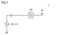
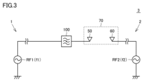
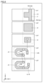
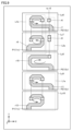
- 1 is a diagram showing a configuration of an antenna device according to a first embodiment; 4 is a graph for explaining frequency characteristics of reactance of the filter device according to the first embodiment; 1 is a diagram showing a configuration of an antenna module according to a first embodiment; 1 is a basic circuit diagram of a filter device according to a first embodiment; 1 is a detailed circuit diagram of a filter device according to a first embodiment; 1 is an external view of a filter device according to a first embodiment; 1 is a perspective view showing a layered structure of a filter device according to a first embodiment; 1 is an exploded plan view showing a layered structure of a filter device according to a first embodiment.
- FIG. 1 is an exploded plan view showing a layered structure of a filter device according to a first embodiment.
- FIG. 1 is an exploded plan view showing a layered structure of a filter device according to a first embodiment.
- FIG. 4 is a detailed circuit diagram for explaining a parasitic capacitance generated in the filter device according to the first embodiment.
- FIG. 4 is a detailed circuit diagram for explaining a parasitic capacitance generated in the filter device according to the first embodiment.
- FIG. 4 is a detailed circuit diagram for explaining a parasitic capacitance generated in the filter device according to the first embodiment.
- FIG. 5 is a graph showing an example of an insertion loss of the filter device according to the first embodiment.
- FIG. 11 is a detailed circuit diagram of a filter device according to a second embodiment.
- FIG. 11 is a perspective view showing a layered structure of a filter device according to a second embodiment.
- 11 is an exploded plan view showing a layered structure of a filter device according to a second embodiment.
- FIG. 11 is an exploded plan view showing a layered structure of a filter device according to a second embodiment.
- FIG. 11 is an exploded plan view showing a layered structure of a filter device according to a second embodiment.
- FIG. 10 is a graph showing an example of an insertion loss of a filter device according to a second embodiment.
- FIG. 1 is a diagram showing a configuration of an antenna device 1 according to embodiment 1.
- the antenna device 1 can be mounted on a communication device capable of transmitting and receiving radio waves, such as a mobile terminal such as a mobile phone, a smartphone, a tablet terminal, or a smart watch, or a PC (Personal Computer) equipped with a communication function.
- a mobile terminal such as a mobile phone, a smartphone, a tablet terminal, or a smart watch
- PC Personal Computer
- the antenna device 1 is an example of a "first antenna device” and includes a power feed circuit RF1, a radiating element 50, and a filter device 100.
- the power feed circuit RF1 supplies a high-frequency signal in a specific first frequency band to the radiating element 50.
- the first frequency band is referred to as the f1 band.
- the radiating element 50 is, for example, a monopole antenna, and radiates the high-frequency signal in the f1 band supplied from the power feed circuit RF1 into the air as radio waves.
- the radiating element 50 is not limited to a monopole antenna, and may be a dipole antenna, an inverted F-type antenna, a loop antenna, or the like.
- the filter device 100 is provided between the radiating element 50 and the power supply circuit RF1.
- the filter device 100 is configured to attenuate high-frequency signals in the second frequency band while passing high-frequency signals in the first frequency band (f1 band).
- the second frequency band is referred to as the f2 band.
- the f2 band is a frequency band lower than the first frequency band (f1 band) and close to the f1 band.
- the f1 band is the 5 GHz band (5.15-5.85 GHz) used by Wi-Fi (registered trademark)
- the f2 band is n79 (4.4-5.0 GHz).
- Such a filter device 100 is particularly useful when the antenna device 1 is used in the vicinity of an antenna that transmits and receives radio waves in the f2 band.
- FIG. 2 is a graph for explaining the frequency characteristics of the reactance of the filter device 100 according to the first embodiment.
- the frequency characteristics of the reactance of the filter device 100 are shown in a graph with frequency on the horizontal axis and reactance on the vertical axis.
- the attenuation band due to parallel resonance is the f2 band
- the pass band due to series resonance is the f1 band.
- FIG. 3 is a diagram showing a configuration of the antenna module 3 according to the embodiment 1.
- the antenna module 3 can be mounted on a communication device capable of transmitting and receiving radio waves, such as a mobile phone, a smartphone, a tablet terminal, a smart watch, or the like, or a PC equipped with a communication function.
- the antenna module 3 includes the antenna device 1 according to the first embodiment described above, and an antenna device 2.
- the antenna device 2 is an example of a "second antenna device” and includes a feed circuit RF2 and a radiating element 60.
- the feed circuit RF2 supplies a high-frequency signal in a specific second frequency band (f2 band) to the radiating element 60.
- the radiating element 60 is, for example, a monopole antenna, and radiates the high-frequency signal in the f2 band supplied from the feed circuit RF2 into the air as radio waves.
- the radiating element 60 is not limited to a monopole antenna, and may be a dipole antenna, an inverted F-shaped antenna, a loop antenna, or the like.
- the radiating element 60 is provided on the same substrate 70 as the radiating element 50 of the antenna device 1. Note that in the example of FIG. 3, the radiating element 50 and the radiating element 60 are provided on the same substrate 70, but they may be provided on different substrates as long as they are provided within the same antenna module 3.
- the high-frequency signal in the f2 band radiated from the antenna device 2 is absorbed by the antenna device 1 located near the antenna device 2, degrading the radiation efficiency of the antenna device 2.
- the filter device 100 is configured to attenuate the high-frequency signal in the f2 band radiated from the antenna device 2. That is, the filter device 100 is configured to pass the high-frequency signal in the f1 band supplied from the power supply circuit RF1 to the radiating element 50, while not passing the high-frequency signal in the f2 band radiated from the antenna device 2, thereby suppressing degradation of the radiation efficiency of the antenna device 2. This makes it possible to miniaturize the antenna module by placing multiple antennas close to each other, while suppressing degradation of the antenna characteristics.
- Fig. 4 is a basic circuit diagram of the filter device 100 according to the first embodiment.
- the filter device 100 is a trap filter that attenuates high-frequency signals in a specific frequency band (f2 band) by preventing their passage, and may be a band elimination filter.
- the filter device 100 includes a first terminal P1, a second terminal P2, an inductor L1, and a resonant circuit RS including the inductor L2 and a capacitor C1.
- the filter device 100 can be connected to a transmission line on the power feed circuit RF1 side via the first terminal P1.
- the filter device 100 can be connected to a transmission line on the radiating element 50 side via the second terminal P2.
- the first terminal P1 becomes an input terminal and the second terminal P2 becomes an output terminal.
- a high-frequency signal received by the radiating element 50 is supplied to a circuit on the power feed circuit RF1 side via the filter device 100, the first terminal P1 becomes an output terminal and the second terminal P2 becomes an input terminal.
- the power feed circuit RF1 is connected to the first terminal P1 and the radiating element 50 is connected to the second terminal P2, but the radiating element 50 may be connected to the first terminal P1 and the power feed circuit RF1 may be connected to the second terminal P2. The same effect can be obtained with either connection.
- Inductor L1 is an example of a "first inductor.”
- Inductor L2 is an example of a "second inductor.”
- One end of inductor L1 is connected to first terminal P1.
- the other end of inductor L1 is connected to second terminal P2 via second path TL2, which is a short-circuit path, and is also connected to second terminal P2 via resonant circuit RS provided in first path TL1.
- first path TL1 and second path TL2 are connected in parallel between inductor L1 and second terminal P2, resonant circuit RS is provided in first path TL1, and second path TL2 is short-circuited.
- the resonant circuit RS forms a series resonator by connecting an inductor L2 and a capacitor C1 in series between the inductor L1 and the second terminal P2.
- the inductor L1 and the inductor L2 are connected in series and are magnetically coupled to each other.
- a mutual inductance M is generated between the inductor L1 and the inductor L2.
- the generated mutual inductance M generates a mutual inductance in each of the first path TL1 and the second path TL2, forming a parallel resonator.
- the polarity relationship between the inductor L1 and the inductor L2 may be depolarized or additive.
- inductor L1 and the inductor L2 are magnetically coupled with depolarization (hereinafter also referred to as “depolarized coupling”)
- depolarized coupling a magnetic field is generated in a direction in which the magnetic fluxes passing through the inductor L1 and the inductor L2 weaken each other, and magnetic coupling is performed.
- additive coupling additive polarization
- inductors L1 and L2 are additively coupled.
- inductors L1 and L2 are additively coupled, a mutual inductance +M occurs in the first path TL1, and a mutual inductance -M occurs in the second path TL2.
- inductors L1 and L2 are depolarized.
- inductors L1 and L2 are depolarized, a mutual inductance -M occurs in the first path TL1, and a mutual inductance +M occurs in the second path TL2.
- the filter device 100 functions as a parallel resonator with mutual inductance +M and mutual inductance -M.
- the resonant frequency of such a parallel resonator matches the series resonant frequency f0 of the resonant circuit RS, and becomes the parallel resonant frequency of the attenuation band (f2 band) of the filter device 100.
- the designer can design the parallel resonant frequency of the attenuation band simply by determining the values of the inductor L2 and the capacitor C1 that constitute the resonant circuit RS. In this way, the filter device 100 has a configuration that is extremely advantageous in terms of structural design.
- the designer can change the series resonance frequency of the pass band (f1 band) and bring the pass band (f1 band) due to series resonance closer to the attenuation band (f2 band) due to parallel resonance.
- the designer can configure a filter device 100 having a narrow band in which the attenuation characteristics change sharply near the parallel resonance frequency of the attenuation band (f2 band).
- the coupling coefficient k between inductor L1 and inductor L2 also affects the amount and width of attenuation of high-frequency signals in the attenuation band (f2 band).
- the larger the coupling coefficient k the larger the mutual inductance that is generated, so that high-frequency signals are attenuated more steeply in the attenuation band (f2 band), resulting in good attenuation characteristics.
- inductor L1 affects the pass characteristics of high-frequency signals in the pass band (f1 band)
- the entire filter device 100 becomes larger, making it difficult to miniaturize the filter device 100. Therefore, it is difficult to increase the inductance of inductor L1 or inductor L2 while miniaturizing the filter device 100.
- parasitic capacitance may occur between inductors L1 and L2. Such parasitic capacitance may cause self-resonance in inductor L1 or inductor L2, making it difficult to obtain good pass characteristics.
- the filter device 100 is configured to achieve good attenuation and pass characteristics by attenuating high-frequency signals to a greater extent through parallel resonance while being compact.
- FIG. 5 is a detailed circuit diagram of the filter device 100 according to the first embodiment.
- the filter device 100 includes a plurality of inductors as the inductor L1.
- the inductor L1 includes an inductor L1a and an inductor L1b connected in parallel between the first terminal P1 and the resonant circuit RS.
- the inductor L1a and the inductor L1b are an example of a "first sub-inductor.”
- the filter device 100 includes a plurality of inductors as the inductor L2.
- the inductor L2 includes an inductor L2a and an inductor L2b connected in series between the inductor L1 and the second terminal P2.
- the inductor L2a and the inductor L2b are an example of a "second sub-inductor.”
- each of the parallel-connected inductors L1a and L1b is connected to the first terminal P1, and the other end of each of the inductors L1a and L1b is connected to the inductor L2a.
- inductor L2a is connected to inductor L1a and inductor L1b
- inductor L2b is connected to the capacitor C1. That is, inductor L1a and inductor L1b are each connected in series to inductor L2a at the same potential.
- inductor L1 and inductor L2 are depolarized coupled, generating a coupling coefficient k.
- FIG. 6 is an external view of the filter device 100 according to the first embodiment.
- the filter device 100 is formed as an integrated chip component, for example, and an inductor and a capacitor are provided within an insulator 10 (housing) in which multiple dielectric layers are stacked.
- the longitudinal direction of the filter device 100 (insulator 10) is the X direction
- the lateral direction is the Y direction
- the height direction is the Z direction
- the bottom surface (X-Y plane) of the filter device 100 is the mounting surface that is placed on the mounting board, and when the filter device 100 is mounted on the mounting board, the bottom surface faces the mounting board.
- the filter device 100 includes a first external electrode 11 and a second external electrode 12 that are electrically connected to an inductor pattern or an electrode pattern provided inside the insulator 10.
- the first external electrode 11 corresponds to the first terminal P1 described above.
- the second external electrode 12 corresponds to the second terminal P2 described above.
- the first external electrode 11 has a U-shape and includes an external electrode 11a provided on the bottom surface (X-Y plane) of the insulator 10, an external electrode 11b provided on one side surface (X-Z plane) of the insulator 10, and an external electrode 11c provided on the other side surface (X-Z plane) of the insulator 10.
- the external electrode 11b faces the external electrode 11c, and the ends of the external electrodes 11b and 11c are connected to the ends of the external electrode 11a.
- the second external electrode 12 is disposed at a predetermined distance from the first external electrode 11 along the longitudinal direction (X direction) of the filter device 100 (insulator 10).
- the second external electrode 12 has a U-shape and includes an external electrode 12a provided on the bottom surface (X-Y plane) of the insulator 10, an external electrode 12b provided on one side surface (X-Z plane) of the insulator 10, and an external electrode 12c provided on the other side surface (X-Z plane) of the insulator 10.
- the external electrode 12b faces the external electrode 12c, and the ends of the external electrodes 12b and 12c are connected to the ends of the external electrode 12a.
- FIG. 7 is a perspective view showing the layered structure of the filter device 100 according to the first embodiment. Note that in FIG. 7, the outline of the insulator 10 is omitted in order to easily explain the filter device 100.
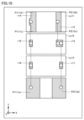
- FIGS. 8 to 10 are exploded plan views showing the layered structure of the filter device 100 according to the first embodiment.
- the filter device 100 is formed by stacking multiple dielectric layers Ly1 to Ly13 in the stacking direction (Z direction) through a stacking process.
- Each dielectric layer Ly1 to Ly13 is a ceramic green sheet, and each electrode pattern and each inductor pattern are formed by printing a conductive paste (for example, Ni paste) using a screen printing method.
- Capacitor C1 is composed of electrode patterns r1 to r3 formed on dielectric layers Ly1 to Ly3, respectively.
- An electrode pattern r1 that constitutes part of the capacitor C1 is formed on the dielectric layer Ly1.
- One end of the electrode pattern r1 is electrically connected to the second terminal P2 (external electrode 12b of the second external electrode 12).
- the other end of the electrode pattern r1 is electrically connected to the second terminal P2 (external electrode 12c of the second external electrode 12).
- An electrode pattern r2 that constitutes part of the capacitor C1 is formed on the dielectric layer Ly2.
- the electrode pattern r2 is not electrically connected to either the first terminal P1 or the second terminal P2, and is also not electrically connected to other electrode patterns.
- An electrode pattern r3 that constitutes part of the capacitor C1 is formed on the dielectric layer Ly3.
- the electrode pattern r3 is electrically connected to the end of the inductor pattern r4 on the dielectric layer Ly4 through a via conductor.
- the capacitor C1 is constructed by utilizing the space formed between the electrode pattern r1 formed on the dielectric layer Ly1 and the electrode pattern r2 formed on the dielectric layer Ly2, and the space formed between the electrode pattern r2 formed on the dielectric layer Ly2 and the electrode pattern r3 formed on the dielectric layer Ly3.
- Inductor L2b is composed of inductor patterns r4 and r5 formed on dielectric layers Ly4 and Ly5, respectively.
- An inductor pattern r4 constituting part of the inductor L2b is formed on the dielectric layer Ly4.
- the inductor pattern r4 is wound around the lamination direction as the winding axis, and is formed on the dielectric layer Ly4 so as to make approximately one full turn clockwise in the figure.
- One end of the inductor pattern r4 is electrically connected to the electrode pattern r3 of the dielectric layer Ly3 through a via conductor.
- the other end of the inductor pattern r4 is electrically connected to the intermediate path portion of the inductor pattern r5 of the dielectric layer Ly5 through a via conductor.
- the intermediate path portion of the inductor pattern r4 is electrically connected to the end of the inductor pattern r5 of the dielectric layer Ly5 through a via conductor.
- An inductor pattern r5 constituting part of the inductor L2b is formed on the dielectric layer Ly5.
- the inductor pattern r5 is wound around the lamination direction as the winding axis, and is formed on the dielectric layer Ly5 so as to make approximately one full turn clockwise in the figure.
- One end of the inductor pattern r5 is electrically connected to the mid-path portion of the inductor pattern r4 on the dielectric layer Ly4 through a via conductor.
- the other end of the inductor pattern r5 is electrically connected to the inductor pattern r6 on the dielectric layer Ly6 through a via conductor.
- the mid-path portion of the inductor pattern r5 is electrically connected to the end of the inductor pattern r4 on the dielectric layer Ly4 through a via conductor.
- inductor L2b when the insulator 10 is viewed from the stacking direction, the inductor pattern r4 of the dielectric layer Ly4 and the inductor pattern r5 of the dielectric layer Ly5 are each configured to have a winding shape wound around the stacking direction as the winding axis.
- Inductor L2a is composed of inductor patterns r6, r8, and r10 formed on dielectric layers Ly6 to Ly8, respectively.
- Inductor L1b is composed of inductor patterns r7 and r9 formed on dielectric layers Ly6 and Ly7, respectively.
- An inductor pattern r6 that constitutes part of the inductor L2a is formed on the dielectric layer Ly6.
- the inductor pattern r6 is electrically connected to an end of the inductor pattern r5 on the dielectric layer Ly5 through a via conductor.
- the inductor pattern r6 is electrically connected to an end of the inductor pattern r8 on the dielectric layer Ly7 through a via conductor.
- an inductor pattern r7 constituting part of the inductor L1b is formed on the dielectric layer Ly6.
- the inductor pattern r7 is wound around the lamination direction as the winding axis, and is formed on the dielectric layer Ly6 so as to make approximately one revolution counterclockwise in the figure.
- One end of the inductor pattern r7 is electrically connected to the second terminal P2 (external electrode 12c of the second external electrode 12).
- the other end of the inductor pattern r7 is electrically connected to the intermediate path portion of the inductor pattern r9 on the dielectric layer Ly7 through a via conductor.
- the intermediate path portion of the inductor pattern r7 is electrically connected to the end of the inductor pattern r9 on the dielectric layer Ly7 through a via conductor.
- An inductor pattern r8 constituting part of the inductor L2a is formed on the dielectric layer Ly7.
- One end of the inductor pattern r8 is electrically connected to the inductor pattern r6 on the dielectric layer Ly6 through a via conductor.
- the other end of the inductor pattern r8 is electrically connected to an end of the inductor pattern r10 on the dielectric layer Ly8 through a via conductor.
- an inductor pattern r9 constituting part of the inductor L1b is formed on the dielectric layer Ly7.
- the inductor pattern r9 is wound around the lamination direction as the winding axis, and is formed on the dielectric layer Ly7 so as to make approximately one revolution counterclockwise in the figure.
- One end of the inductor pattern r9 is electrically connected to the intermediate path portion of the inductor pattern r7 on the dielectric layer Ly6 through a via conductor.
- the other end of the inductor pattern r9 is electrically connected to the first terminal P1 (external electrode 11c of the first external electrode 11).
- the intermediate path portion of the inductor pattern r9 is electrically connected to the end of the inductor pattern r7 on the dielectric layer Ly6 through a via conductor.
- inductor L1b when the insulator 10 is viewed from the stacking direction, the inductor pattern r7 of the dielectric layer Ly6 and the inductor pattern r9 of the dielectric layer Ly7 are each configured to have a winding shape wound around the stacking direction as the winding axis.
- An inductor pattern r10 constituting part of the inductor L2a is formed on the dielectric layer Ly8.
- the inductor pattern r10 is wound around the stacking direction as the winding axis, and is formed on the dielectric layer Ly8 so as to make approximately one full turn clockwise in the figure.
- One end of the inductor pattern r10 is electrically connected to the end of the inductor pattern r8 on the dielectric layer Ly7 through a via conductor.
- the other end of the inductor pattern r10 is electrically connected to the second terminal P2 (external electrode 12c of the second external electrode 12).
- the inductor pattern r10 of the dielectric layer Ly8 is configured to have a winding shape wound around the stacking direction as the winding axis.
- the inductor L1a is composed of inductor patterns r11 and r12 formed on the dielectric layers Ly9 and Ly10, respectively.
- the dielectric layer Ly9 is provided with an inductor pattern r11 that constitutes part of the inductor L1a.
- the inductor pattern r11 is wound around the lamination direction as the winding axis, and is formed on the dielectric layer Ly9 so as to make approximately one full turn counterclockwise in the figure.
- One end of the inductor pattern r11 is electrically connected to the second terminal P2 (external electrode 12c of the second external electrode 12).
- the other end of the inductor pattern r11 is electrically connected to the intermediate path portion of the inductor pattern r12 on the dielectric layer Ly10 through a via conductor.
- the intermediate path portion of the inductor pattern r11 is electrically connected to the end of the inductor pattern r12 on the dielectric layer Ly10 through a via conductor.
- the dielectric layer Ly10 is provided with an inductor pattern r12 that constitutes part of the inductor L1a.
- the inductor pattern r12 is wound around the lamination direction as the winding axis, and is formed on the dielectric layer Ly10 so as to make approximately one full turn counterclockwise in the figure.
- One end of the inductor pattern r12 is electrically connected to the intermediate path portion of the inductor pattern r11 on the dielectric layer Ly9 through a via conductor.
- the other end of the inductor pattern r12 is electrically connected to the first terminal P1 (external electrode 11c of the first external electrode 11).
- the intermediate path portion of the inductor pattern r12 is electrically connected to the end of the inductor pattern r11 on the dielectric layer Ly9 through a via conductor.
- the inductor pattern r11 of the dielectric layer Ly9 and the inductor pattern r12 of the dielectric layer Ly10 are each configured to have a winding shape wound around the stacking direction as the winding axis.
- one end of the inductor pattern r7 of the dielectric layer Ly6 constituting part of the inductor L1b, one end of the inductor pattern r10 of the dielectric layer Ly8 constituting part of the inductor L2a, and one end of the inductor pattern r11 of the dielectric layer Ly9 constituting part of the inductor L1a are electrically connected via the first terminal P1 (external electrode 11c of the first external electrode 11).
- the inductor L1a, inductor L1b, and inductor L2a are connected at the same potential.
- An electrode pattern r13 is formed on the dielectric layer Ly11. One end of the electrode pattern r13 is electrically connected to the second terminal P2 (external electrode 12b of the second external electrode 12), and the other end of the electrode pattern r13 is electrically connected to the second terminal P2 (external electrode 12c of the second external electrode 12). An intermediate path portion of the electrode pattern r13 is electrically connected to the electrode pattern r15 of the dielectric layer Ly12 through a via conductor.
- an electrode pattern r14 is formed on the dielectric layer Ly11. One end of the electrode pattern r14 is electrically connected to the first terminal P1 (external electrode 11b of the first external electrode 11), and the other end of the electrode pattern r14 is electrically connected to the first terminal P1 (external electrode 11c of the first external electrode 11). An intermediate path portion of the electrode pattern r14 is electrically connected to the electrode pattern r16 of the dielectric layer Ly12 through a via conductor.
- An electrode pattern r15 is formed on the dielectric layer Ly12.
- the electrode pattern r15 is electrically connected to an intermediate path portion of the electrode pattern r13 on the dielectric layer Ly11 through a via conductor.
- the electrode pattern r15 is also electrically connected to the electrode pattern r17 on the dielectric layer Ly13 through a via conductor.
- an electrode pattern r16 is formed on the dielectric layer Ly12.
- the electrode pattern r16 is electrically connected to an intermediate path portion of the electrode pattern r14 on the dielectric layer Ly11 through a via conductor.
- the electrode pattern r16 is also electrically connected to the electrode pattern r18 on the dielectric layer Ly13 through a via conductor.
- An electrode pattern r17 is formed on the dielectric layer Ly13.
- the electrode pattern r17 is electrically connected to the electrode pattern r15 of the dielectric layer Ly12 through a via conductor.
- the electrode pattern r17 is also electrically connected to the second terminal P2 (external electrode 12a of the second external electrode 12) through a via conductor.
- an electrode pattern r18 is formed on the dielectric layer Ly13.
- the electrode pattern r18 is electrically connected to the electrode pattern r16 of the dielectric layer Ly12 through a via conductor.
- the electrode pattern r18 is also electrically connected to the first terminal P1 (the external electrode 11a of the first external electrode 11) through a via conductor.
- the inductors L1a, L1b, L2a, and L2b are arranged to face each other in the stacking direction, and when the insulator 10 is viewed from the stacking direction, at least a portion of each of the openings of the inductors L1a and L1b overlaps with each of the openings of the inductors L2a and L2b.
- the inductors L1 and L2 are arranged alternately in the stacking direction and are magnetically coupled. Specifically, as shown in Figures 7 to 9, the inductors L1a and L1b included in the inductor L1 and the inductors L2a and L2b included in the inductor L2 are arranged alternately in the stacking direction.
- inductor patterns r11 and r12 constituting inductor L1a (inductor L1), inductor pattern r10 constituting inductor L2a (inductor L2), inductor patterns r7 and r9 constituting inductor L1b (inductor L1), and inductor patterns r4 and r5 constituting inductor L2b (inductor L2) are arranged in this order along the stacking direction from the bottom surface on which the external electrodes 11a and 12a are provided to the top surface.
- the inductor pattern r10 constituting the inductor L2a is arranged so as to be sandwiched in the stacking direction between the inductor patterns r11 and r12 constituting the inductor L1a (inductor L1) and the inductor patterns r7 and r9 constituting the inductor L1b (inductor L1).
- the inductor patterns r7 and r9 constituting the inductor L1b (inductor L1) are arranged so as to be sandwiched in the stacking direction between the inductor pattern r10 constituting the inductor L2a (inductor L2) and the inductor patterns r4 and r5 constituting the inductor L2b (inductor L2).
- the filter device 100 configured as described above can increase the coupling coefficient k between the inductor L1 (inductors L1a, L1b) and the inductor L2 (inductors L2a, L2b) by placing the multiple inductors L1a, L1b constituting the inductor L1 and the multiple inductors L2a, L2b constituting the inductor L2 close to each other without increasing the number of turns of the inductor L2 or increasing the opening area of the inductor L2. This allows the filter device 100 to attenuate high-frequency signals more significantly through parallel resonance while being compact, and to obtain good attenuation and passing characteristics.
- Figs. 11 to 13 are detailed circuit diagrams for explaining the parasitic capacitance that occurs in filter device 100 according to embodiment 1. Note that Fig. 13 shows a circuit diagram that has been modified from the circuit diagram shown in Fig. 12 for easier viewing.
- a parasitic capacitance Cp may be generated between inductors L1a and L2a. Also, when inductors L1b and L2a are close to each other, a parasitic capacitance Cp may be generated between inductors L1a and L2a.
- inductor L1a and inductor L1b are each connected in series with inductor L2a at the same potential, and further, the second path TL2 (short-circuit path) is connected in parallel to the above-mentioned parasitic capacitance Cp. Therefore, the presence of the second path TL2 (short-circuit path) makes the filter device 100 less susceptible to the effects of the parasitic capacitance Cp. In this way, the filter device 100 can ignore the parasitic capacitance Cp between inductor L1a and inductor L2a.
- the proximity of inductor L1a and inductor L2b may cause parasitic capacitance Cp to occur between inductor L1a and inductor L2b.
- inductors L1b and L2a are provided between inductors L1a and L2b, the proximity between inductors L1a and L2b is not high, but some parasitic capacitance Cp may occur.
- the proximity of inductors L1b and L2b may cause parasitic capacitance Cp to occur between inductors L1b and L2b.
- the above-mentioned parasitic capacitance Cp is connected in parallel with the capacitor C1 of the resonant circuit RS. Therefore, in the filter device 100, the parasitic capacitance Cp can be used in place of the capacitor C1, or the parasitic capacitance Cp can be used as part of the capacitor C1. In this way, the filter device 100 can use the parasitic capacitance Cp between the inductors L1a and L2b and the parasitic capacitance Cp between the inductors L1b and L2b as the capacitor C1, so that the capacitor C1 can be made smaller.
- the designer can arrange the electrode patterns constituting the capacitor C1 so as to avoid the openings of the inductors L1a, L1b, L2a, and L2b, so that the effect of the capacitor C1 on the inductors L1a, L1b, L2a, and L2b can be minimized.
- the filter device 100 can avoid self-resonance in inductor L1 or inductor L2 due to the parasitic capacitance that occurs when inductor L1 and inductor L2 are placed close to each other, thereby achieving good pass characteristics.
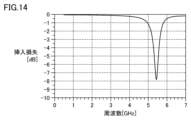
- FIG. 14 is a graph showing an example of the insertion loss of the filter device 100 according to the first embodiment.
- the frequency characteristics of the insertion loss of the filter device 100 are shown in a graph with frequency on the horizontal axis and insertion loss on the vertical axis.
- the filter device 100 can use parallel resonance to steeply and largely attenuate high-frequency signals in the attenuation band, while using series resonance to pass high-frequency signals in the pass band with minimal attenuation.
- the filter device 100 can achieve good attenuation and transmission characteristics while being compact.
- a filter device 200 according to the second embodiment will be described with reference to Fig. 15 to Fig. 20. Only the parts of the filter device 200 according to the second embodiment that are different from the filter device 100 according to the first embodiment will be described below.
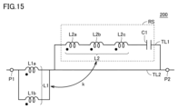
- FIG. 15 is a detailed circuit diagram of a filter device 200 according to embodiment 2.
- the number of inductors (inductors L1a, L1b) included in inductor L1 is the same as the number of inductors (inductors L2a, L2b) included in inductor L2.
- the number of inductors included in inductor L2 is greater than the number of inductors included in inductor L1.
- the filter device 200 according to the second embodiment is not limited to a configuration in which the inductors included in inductor L1 and the inductors included in inductor L2 are stacked alternately one by one, but also includes a configuration in which the inductors included in inductor L1 and the inductors included in inductor L2 are stacked alternately in groups of multiple inductors.
- the filter device 200 includes, as the inductor L1, inductors L1a and L1b connected in parallel between the first terminal P1 and the resonant circuit RS, and, as the inductor L2, inductors L2a, L2b, and L2c connected in series between the inductor L1 and the second terminal P2.
- Inductors L1a and L1b are examples of a "first sub-inductor”
- inductors L2a, L2b, and L2c are examples of a "second sub-inductor”.
- inductor L2a is connected to inductors L1a and L1b, and inductor L2c is connected to capacitor C1.
- inductors L1 and L2 are additively coupled, generating a coupling coefficient k. Note that inductors L1 and L2 may also be depolarized.
- FIG. 16 is a perspective view showing the layered structure of the filter device 200 according to the second embodiment. Note that in FIG. 16, the outline of the insulator 10 is omitted in order to easily explain the filter device 200.
- FIGS. 17 to 19 are exploded plan views showing the layered structure of the filter device 200 according to the second embodiment.
- the filter device 200 is formed by stacking multiple dielectric layers Ly21 to Ly33 in the stacking direction (Z direction) using a stacking process.
- Each dielectric layer Ly21 to Ly33 is a ceramic green sheet, and each electrode pattern and each inductor pattern are formed by printing a conductive paste (for example, Ni paste) using a screen printing method.
- Inductor L2a is composed of inductor patterns r21, r22, r24, and r26 formed on dielectric layers Ly21 to Ly24, respectively.
- Inductor L1b is composed of inductor patterns r23 and r25 formed on dielectric layers Ly22 and Ly23, respectively.
- An inductor pattern r21 that constitutes part of the inductor L2a is formed on the dielectric layer Ly21.
- the inductor pattern r21 is wound around the stacking direction as the winding axis, and is formed on the dielectric layer Ly21 so as to make approximately one full turn clockwise in the figure.
- One end of the inductor pattern r21 is electrically connected to the inductor pattern r22 of the dielectric layer Ly22 through a via conductor.
- the other end of the inductor pattern r21 is electrically connected to the second terminal P2 (external electrode 12c of the second external electrode 12).
- An inductor pattern r22 that constitutes part of the inductor L2a is formed on the dielectric layer Ly22.
- the inductor pattern r22 is electrically connected to an end of the inductor pattern r21 on the dielectric layer Ly21 through a via conductor.
- the inductor pattern r22 is electrically connected to the inductor pattern r24 on the dielectric layer Ly23 through a via conductor.
- an inductor pattern r23 constituting a part of the inductor L1b is formed on the dielectric layer Ly22.
- the inductor pattern r23 is wound around the lamination direction as the winding axis, and is formed on the dielectric layer Ly22 so as to make approximately one full turn clockwise in the figure.
- One end of the inductor pattern r23 is electrically connected to the intermediate path portion of the inductor pattern r25 on the dielectric layer Ly23 through a via conductor.
- the other end of the inductor pattern r23 is electrically connected to the first terminal P1 (external electrode 11b of the first external electrode 11).
- the intermediate path portion of the inductor pattern r23 is electrically connected to the end of the inductor pattern r25 on the dielectric layer Ly23 through a via conductor.
- An inductor pattern r24 that constitutes part of the inductor L2a is formed on the dielectric layer Ly23.
- the inductor pattern r24 is electrically connected to the inductor pattern r22 on the dielectric layer Ly22 through a via conductor. Furthermore, the inductor pattern r24 is electrically connected to an end of the inductor pattern r26 on the dielectric layer Ly24 through a via conductor.
- an inductor pattern r25 constituting a part of the inductor L1b is formed on the dielectric layer Ly23.
- the inductor pattern r25 is wound around the lamination direction as the winding axis, and is formed on the dielectric layer Ly23 so as to make approximately one full turn clockwise in the figure.
- One end of the inductor pattern r25 is electrically connected to the second terminal P2 (external electrode 12b of the second external electrode 12).
- the other end of the inductor pattern r25 is electrically connected to the intermediate path portion of the inductor pattern r23 on the dielectric layer Ly22 through a via conductor.
- the intermediate path portion of the inductor pattern r25 is electrically connected to the end of the inductor pattern r23 on the dielectric layer Ly22 through a via conductor.
- An inductor pattern r26 that constitutes part of the inductor L2a is formed on the dielectric layer Ly24.
- the inductor pattern r26 is wound around the lamination direction as the winding axis, and is formed on the dielectric layer Ly24 so as to make approximately half a turn clockwise in the figure.
- One end of the inductor pattern r26 is electrically connected to an end of the inductor pattern r27 of the dielectric layer Ly25 through a via conductor.
- the other end of the inductor pattern r26 is electrically connected to the inductor pattern r24 of the dielectric layer Ly23 through a via conductor.
- inductor L2a when the insulator 10 is viewed from the stacking direction, the inductor pattern r21 of the dielectric layer Ly21 and the inductor pattern r26 of the dielectric layer Ly24 are each configured to have a winding shape wound around the stacking direction as the winding axis.
- inductor L1b when the insulator 10 is viewed from the stacking direction, the inductor pattern r23 of the dielectric layer Ly22 and the inductor pattern r25 of the dielectric layer Ly23 are each configured to have a winding shape wound around the stacking direction as the winding axis.
- Inductor L2b is composed of inductor patterns r27 and r28 formed on dielectric layers Ly25 and Ly26, respectively.
- An inductor pattern r27 that constitutes part of the inductor L2b is formed on the dielectric layer Ly25.
- the inductor pattern r27 is wound around the lamination direction as the winding axis, and is formed on the dielectric layer Ly25 so as to make approximately one full turn clockwise in the figure.
- One end of the inductor pattern r27 is electrically connected to an end of the inductor pattern r28 on the dielectric layer Ly26 via a via conductor.
- the other end of the inductor pattern r27 is electrically connected to an end of the inductor pattern r26 on the dielectric layer Ly24 via a via conductor.
- An inductor pattern r28 that constitutes part of the inductor L2b is formed on the dielectric layer Ly26.
- the inductor pattern r28 is wound around the lamination direction as the winding axis, and is formed on the dielectric layer Ly26 so as to make approximately half a turn clockwise in the figure.
- One end of the inductor pattern r28 is electrically connected to an end of the inductor pattern r27 of the dielectric layer Ly25 through a via conductor.
- the other end of the inductor pattern r28 is electrically connected to the inductor pattern r29 of the dielectric layer Ly27 through a via conductor.
- inductor L2b when the insulator 10 is viewed from the stacking direction, the inductor pattern r27 of the dielectric layer Ly25 and the inductor pattern r28 of the dielectric layer Ly26 are each configured to have a winding shape wound around the stacking direction as the winding axis.
- Inductor L1a is composed of inductor patterns r30 and r32 formed on dielectric layers Ly27 and Ly28, respectively.
- An inductor pattern r29 that constitutes part of the inductor L2b is formed on the dielectric layer Ly27.
- One end of the inductor pattern r29 is electrically connected to an end of the inductor pattern r28 on the dielectric layer Ly26 through a via conductor.
- the other end of the inductor pattern r29 is electrically connected to an end of the inductor pattern r31 on the dielectric layer Ly28 through a via conductor.
- an inductor pattern r30 constituting a part of the inductor L1a is formed on the dielectric layer Ly27.
- the inductor pattern r30 is wound around the lamination direction as the winding axis, and is formed on the dielectric layer Ly27 so as to make approximately one full turn clockwise in the figure.
- One end of the inductor pattern r30 is electrically connected to the intermediate path portion of the inductor pattern r32 on the dielectric layer Ly28 through a via conductor.
- the other end of the inductor pattern r30 is electrically connected to the first terminal P1 (external electrode 11b of the first external electrode 11).
- the intermediate path portion of the inductor pattern r30 is electrically connected to the end of the inductor pattern r32 on the dielectric layer Ly28 through a via conductor.
- An inductor pattern r31 that constitutes part of the inductor L2c is formed on the dielectric layer Ly28.
- One end of the inductor pattern r31 is electrically connected to an end of the inductor pattern r29 on the dielectric layer Ly27 through a via conductor.
- the other end of the inductor pattern r31 is electrically connected to an end of the inductor pattern r33 on the dielectric layer Ly29 through a via conductor.
- an inductor pattern r32 constituting a part of the inductor L1a is formed on the dielectric layer Ly28.
- the inductor pattern r32 is wound around the lamination direction as the winding axis, and is formed on the dielectric layer Ly28 so as to make approximately one full turn clockwise in the figure.
- One end of the inductor pattern r32 is electrically connected to the second terminal P2 (external electrode 12b of the second external electrode 12).
- the other end of the inductor pattern r32 is electrically connected to the intermediate path portion of the inductor pattern r30 on the dielectric layer Ly27 through a via conductor.
- the intermediate path portion of the inductor pattern r32 is electrically connected to the end of the inductor pattern r30 on the dielectric layer Ly27 through a via conductor.
- the inductor pattern r30 of the dielectric layer Ly27 and the inductor pattern r32 of the dielectric layer Ly28 are each configured to have a winding shape wound around the stacking direction as the winding axis.
- Inductor L2c is composed of an inductor pattern r33 formed on the dielectric layer Ly29.
- the inductor pattern r33 constituting the inductor L2c is formed on the dielectric layer Ly29.
- the inductor pattern r33 is wound around the lamination direction as the winding axis, and is formed on the dielectric layer Ly29 so as to make approximately one full turn clockwise in the figure.
- One end of the inductor pattern r33 is electrically connected to the inductor pattern r34 of the dielectric layer Ly30 through a via conductor.
- the other end of the inductor pattern r33 is electrically connected to the inductor pattern r31 of the dielectric layer Ly28 through a via conductor.
- inductor L2c when the insulator 10 is viewed from the stacking direction, the inductor pattern r33 of the dielectric layer Ly29 is configured to have a winding shape wound around the stacking direction as the winding axis.
- Capacitor C1 is composed of electrode patterns r34 and r35 formed on dielectric layers Ly30 and Ly31, respectively.
- An electrode pattern r34 that constitutes part of the capacitor C1 is formed on the dielectric layer Ly30.
- the electrode pattern r34 is electrically connected to the end of the inductor pattern r33 of the dielectric layer Ly29 through a via conductor.
- An electrode pattern r35 constituting a part of the capacitor C1 is formed on the dielectric layer Ly31.
- One end of the electrode pattern r35 is electrically connected to the second terminal P2 (external electrode 12b of the second external electrode 12).
- the other end of the electrode pattern r35 is electrically connected to the second terminal P2 (external electrode 12c of the second external electrode 12).
- the intermediate path portion of the inductor pattern r35 is electrically connected to the electrode pattern r37 of the dielectric layer Ly32 through a via conductor.
- an electrode pattern r36 is formed on the dielectric layer Ly31.
- One end of the electrode pattern r36 is electrically connected to the first terminal P1 (external electrode 11b of the first external electrode 11).
- the other end of the electrode pattern r36 is electrically connected to the first terminal P1 (external electrode 11c of the first external electrode 11).
- An intermediate path portion of the inductor pattern r36 is electrically connected to the electrode pattern r38 of the dielectric layer Ly32 through a via conductor.
- the capacitor C1 is constructed by utilizing the space formed between the electrode pattern r34 formed on the dielectric layer Ly30 and the electrode pattern r35 formed on the dielectric layer Ly31.
- An electrode pattern r37 is formed on the dielectric layer Ly32.
- the electrode pattern r37 is electrically connected to an intermediate path portion of the electrode pattern r35 of the dielectric layer Ly31 through a via conductor.
- the electrode pattern r37 is also electrically connected to the electrode pattern r39 of the dielectric layer Ly33 through a via conductor.
- an electrode pattern r38 is formed on the dielectric layer Ly32.
- the electrode pattern r38 is electrically connected to an intermediate path portion of the electrode pattern r36 of the dielectric layer Ly31 through a via conductor.
- the electrode pattern r38 is also electrically connected to the electrode pattern r40 of the dielectric layer Ly33 through a via conductor.
- An electrode pattern r39 is formed on the dielectric layer Ly33.
- the electrode pattern r39 is electrically connected to the electrode pattern r37 of the dielectric layer Ly32 through a via conductor.
- the electrode pattern r39 is also electrically connected to the second terminal P2 (external electrode 12a of the second external electrode 12) through a via conductor.
- an electrode pattern r40 is formed on the dielectric layer Ly33.
- the electrode pattern r40 is electrically connected to the electrode pattern r38 of the dielectric layer Ly32 through a via conductor.
- the electrode pattern r40 is also electrically connected to the first terminal P1 (the external electrode 11a of the first external electrode 11) through a via conductor.
- inductors L1a, L1b, L2a, L2b, and L2c are arranged to face each other in the stacking direction, and when the insulator 10 is viewed from the stacking direction, at least a portion of each of the openings of inductors L1a and L1b overlaps with each of the openings of inductors L2a, L2b, and L2c.
- the inductors L1 and L2 are arranged alternately in the stacking direction and are magnetically coupled. Specifically, as shown in Figures 16 to 19, the inductors L1a and L1b included in the inductor L1 and the inductors L2a, L2b, and L2c included in the inductor L2 are arranged alternately in the stacking direction.
- inductor pattern r33 constituting inductor L2c (inductor L2)
- inductor patterns r30 and r32 constituting inductor L1a (inductor L1)
- inductor patterns r27 and r28 constituting inductor L2b (inductor L2)
- inductor pattern r26 constituting inductor L2a (inductor L2)
- inductor patterns r23 and r25 constituting inductor L1b (inductor L1)
- inductor pattern r21 constituting inductor L2a (inductor L2).
- the inductor patterns r23 and r25 constituting the inductor L1b are arranged so as to be sandwiched between the inductor pattern r21 constituting the inductor L2a (inductor L2) and the inductor pattern r26 constituting the inductor L2a (inductor L2) in the stacking direction.
- the inductor pattern r26 constituting the inductor L2a (inductor L2) and the inductor patterns r27 and r28 constituting the inductor L2b (inductor L2) are arranged so as to be sandwiched between the inductor patterns r23 and r25 constituting the inductor L1b (inductor L1) and the inductor patterns r30 and r32 constituting the inductor L1a (inductor L1) in the stacking direction.
- the inductor patterns r30 and r32 constituting the inductor L1a are arranged so as to be sandwiched between the inductor patterns r27 and r28 constituting the inductor L2b (inductor L2) and the inductor pattern r33 constituting the inductor L2c (inductor L2).
- the number of inductors included in the inductor L2 is greater than the number of inductors included in the inductor L1. Furthermore, in the filter device 200, the multiple inductors L2 (inductors L2a, L2b) are arranged so as to be sandwiched between the two inductors L1 (inductors L1b, L1a) in the stacking direction.
- the filter device 200 configured as described above can increase the coupling coefficient k between the inductor L1 (inductors L1a, L1b) and the inductor L2 (inductors L2a, L2b, L2c) by placing the multiple inductors L1a, L1b constituting the inductor L1 close to the multiple inductors L2a, L2b, L2c constituting the inductor L2, without increasing the number of turns of the inductor L2 or increasing the opening area of the inductor L2.
- This allows the filter device 200 to attenuate high-frequency signals more significantly through parallel resonance while being compact, and to obtain good attenuation and passing characteristics.
- the filter device 200 can ignore the parasitic capacitance Cp between the inductor L1a and the inductor L2a, and can utilize the parasitic capacitance Cp between the inductor L1a and each of the inductors L2b and L2c as the capacitor C1. Therefore, the filter device 200 can avoid the occurrence of self-resonance in the inductor L1 or the inductor L2 due to the parasitic capacitance that occurs when the inductor L1 and the inductor L2 are placed close to each other, and can obtain good pass characteristics.
- the number of inductors included in inductor L1 may be one or more, and the number of inductors included in inductor L2 may be one or more.
- at least one of inductor L1 and inductor L2 may include multiple inductors, and inductor L1 and inductor L2 may be arranged alternately in the stacking direction and magnetically coupled.
- the filter device may include one inductor L1 and multiple inductors L2, and the inductors may be arranged in the stacking direction such that the multiple inductors L2 sandwich the single inductor L1.
- the filter device may include multiple inductors L1 and one inductor L2, and the inductors may be arranged in the stacking direction such that the multiple inductors L1 sandwich the one inductor L2.
- the filter device may include multiple inductors L1 and multiple inductors L2, with one inductor L1 and one inductor L2 arranged alternately in the stacking direction.
- the inductors may be arranged such that multiple inductors L1 sandwich multiple inductors L2 in the stacking direction.
- the inductors may be arranged such that multiple inductors L2 sandwich multiple inductors L1 in the stacking direction.
- a filter device (100, 200) includes an insulator (10) including a first external electrode (11) and a second external electrode (12), a first inductor (L1) connected to the first external electrode, and a resonant circuit (RS) including a second inductor (L2) and a capacitor (C1).
- the first inductor is connected to the second external electrode and is also connected to the resonant circuit.
- the first inductor and the second inductor are laminated in the insulator. At least one of the first inductor and the second inductor includes a plurality of inductor patterns. The first inductor and the second inductor are alternately arranged in the lamination direction and are magnetically coupled.
- the filter device described in 1 is a two-terminal filter consisting of a first external electrode and a second external electrode, which passes high-frequency signals in a first frequency band and attenuates high-frequency signals in a second frequency band that is lower than the first frequency band.
- a second inductor and a capacitor are connected in series between the first inductor and the second external electrode.
- a first inductor and a second inductor are connected in series between the first external electrode and the second external electrode.
- the first inductor includes a plurality of first sub-inductors (L1a, L1b) connected in parallel between the first external electrode and the resonant circuit.
- the second inductor includes a plurality of second sub-inductors (L2a, L2b, L2c) connected in series between the first inductor and the second external electrode.
- the first inductor includes a plurality of first sub-inductors (L1a, L1b).
- the second inductor includes at least one second sub-inductor (L2a). The at least one second sub-inductor is sandwiched between the plurality of first sub-inductors in the stacking direction.
- the first inductor includes a plurality of first sub-inductors (L1a, L1b).
- the second inductor includes a plurality of second sub-inductors (L2a, L2b).
- the plurality of first sub-inductors and the plurality of second sub-inductors are arranged alternately in the stacking direction.
- the multiple first sub-inductors are connected in parallel between the first external electrode and the resonant circuit.
- the multiple second sub-inductors are connected in series between the first inductor and the second external electrode.
- Each of the multiple first sub-inductors and one of the multiple second sub-inductors are connected in series at the same potential.
- the first inductor is wound around the stacking direction as its winding axis.
- the second inductor is wound around the stacking direction as its winding axis.
- the number of second sub-inductors (L2a, L2b, L2c) included in the second inductor is greater than the number of first sub-inductors (L1a, L1b) included in the first inductor.
- An antenna device (1) includes a radiating element (50) that radiates a high-frequency signal in a first frequency band as radio waves, a power supply circuit (RF1) that supplies the high-frequency signal in the first frequency band to the radiating element, and a filter device (100, 200) that is provided between the radiating element and the power supply circuit.
- An antenna module (3) includes a first antenna device (1) that radiates a high-frequency signal in a first frequency band as radio waves, and a second antenna device (2) that radiates a high-frequency signal in a second frequency band as radio waves.
- the first antenna device is the antenna device (1) described in Item 12.
- Antenna device 1, 2 Antenna device, 3 Antenna module, 10 Insulator, 11 First external electrode, 11a, 11b, 11c, 12a, 12b, 12c External electrodes, 12 Second external electrode, 50, 60 Radiating element, 70 Substrate, 100, 200 Filter device, C1 Capacitor, Cp Parasitic capacitance, L1a, L1b, L1, L2a, L2b, L2c, L2 Inductor, P1 First terminal, P2 Second terminal, RF1, RF2 Power supply circuit, RS Resonant circuit, TL1 First path, TL2 Second path.
Landscapes
- Engineering & Computer Science (AREA)
- Power Engineering (AREA)
- Microelectronics & Electronic Packaging (AREA)
- Filters And Equalizers (AREA)
Priority Applications (2)
| Application Number | Priority Date | Filing Date | Title |
|---|---|---|---|
| CN202480052807.1A CN121693857A (zh) | 2023-09-07 | 2024-06-24 | 滤波器装置、天线装置以及天线模块 |
| JP2025544152A JPWO2025052761A1 (https=) | 2023-09-07 | 2024-06-24 |
Applications Claiming Priority (2)
| Application Number | Priority Date | Filing Date | Title |
|---|---|---|---|
| JP2023-144923 | 2023-09-07 | ||
| JP2023144923 | 2023-09-07 |
Publications (1)
| Publication Number | Publication Date |
|---|---|
| WO2025052761A1 true WO2025052761A1 (ja) | 2025-03-13 |
Family
ID=94923124
Family Applications (1)
| Application Number | Title | Priority Date | Filing Date |
|---|---|---|---|
| PCT/JP2024/022810 Pending WO2025052761A1 (ja) | 2023-09-07 | 2024-06-24 | フィルタ装置、アンテナ装置、およびアンテナモジュール |
Country Status (3)
| Country | Link |
|---|---|
| JP (1) | JPWO2025052761A1 (https=) |
| CN (1) | CN121693857A (https=) |
| WO (1) | WO2025052761A1 (https=) |
Citations (5)
| Publication number | Priority date | Publication date | Assignee | Title |
|---|---|---|---|---|
| JPH04199804A (ja) * | 1990-11-29 | 1992-07-21 | Murata Mfg Co Ltd | 積層チップ型コイル部品及びその製造方法 |
| WO2012153690A1 (ja) * | 2011-05-09 | 2012-11-15 | 株式会社村田製作所 | 結合度調整回路、アンテナ装置および通信端末装置 |
| WO2014050482A1 (ja) * | 2012-09-28 | 2014-04-03 | 株式会社村田製作所 | インピーダンス変換回路の設計方法 |
| WO2018012400A1 (ja) * | 2016-07-15 | 2018-01-18 | 株式会社村田製作所 | 高周波トランスおよび移相器 |
| WO2023080009A1 (ja) * | 2021-11-02 | 2023-05-11 | 株式会社村田製作所 | フィルタ装置、アンテナ装置、およびアンテナモジュール |
-
2024
- 2024-06-24 JP JP2025544152A patent/JPWO2025052761A1/ja active Pending
- 2024-06-24 CN CN202480052807.1A patent/CN121693857A/zh active Pending
- 2024-06-24 WO PCT/JP2024/022810 patent/WO2025052761A1/ja active Pending
Patent Citations (5)
| Publication number | Priority date | Publication date | Assignee | Title |
|---|---|---|---|---|
| JPH04199804A (ja) * | 1990-11-29 | 1992-07-21 | Murata Mfg Co Ltd | 積層チップ型コイル部品及びその製造方法 |
| WO2012153690A1 (ja) * | 2011-05-09 | 2012-11-15 | 株式会社村田製作所 | 結合度調整回路、アンテナ装置および通信端末装置 |
| WO2014050482A1 (ja) * | 2012-09-28 | 2014-04-03 | 株式会社村田製作所 | インピーダンス変換回路の設計方法 |
| WO2018012400A1 (ja) * | 2016-07-15 | 2018-01-18 | 株式会社村田製作所 | 高周波トランスおよび移相器 |
| WO2023080009A1 (ja) * | 2021-11-02 | 2023-05-11 | 株式会社村田製作所 | フィルタ装置、アンテナ装置、およびアンテナモジュール |
Also Published As
| Publication number | Publication date |
|---|---|
| JPWO2025052761A1 (https=) | 2025-03-13 |
| CN121693857A (zh) | 2026-03-17 |
Similar Documents
| Publication | Publication Date | Title |
|---|---|---|
| JP4900515B1 (ja) | アンテナ装置および通信端末装置 | |
| JP5655962B2 (ja) | アンテナ装置および無線通信装置 | |
| JP4962629B2 (ja) | 高周波トランス、電子回路および電子機器 | |
| CN102474005B (zh) | 稳频电路、稳频器件、天线装置、及通信终端设备 | |
| JP5910779B2 (ja) | インピーダンス整合切替回路、アンテナ装置および通信端末装置 | |
| JP4935955B2 (ja) | アンテナ装置および通信端末装置 | |
| JP5234084B2 (ja) | アンテナ装置および通信端末装置 | |
| JP5477512B2 (ja) | インピーダンス変換回路および通信端末装置 | |
| WO2017035726A1 (zh) | 一种用于多频天线双极化的天线振子 | |
| JP5957816B2 (ja) | インピーダンス変換デバイス、アンテナ装置および通信端末装置 | |
| JP6269902B2 (ja) | アンテナ装置および電子機器 | |
| WO2013114978A1 (ja) | 無線通信モジュール、及びそれを用いた通信端末装置 | |
| US8797225B2 (en) | Antenna device and communication terminal apparatus | |
| US20240235516A1 (en) | Filter device, antenna device, and antenna module | |
| WO2025052761A1 (ja) | フィルタ装置、アンテナ装置、およびアンテナモジュール | |
| JP2019192951A (ja) | アンテナ装置および電子機器 | |
| JP2013168780A (ja) | 表面実装型アンテナ | |
| WO2025052762A1 (ja) | フィルタ装置、アンテナ装置、およびアンテナモジュール | |
| JP7593496B2 (ja) | フィルタ装置、アンテナ装置、およびアンテナモジュール | |
| JPWO2023276879A5 (https=) | ||
| JP5736949B2 (ja) | 高周波回路モジュール | |
| JP6566181B1 (ja) | 複合アンテナ素子 |
Legal Events
| Date | Code | Title | Description |
|---|---|---|---|
| 121 | Ep: the epo has been informed by wipo that ep was designated in this application |
Ref document number: 24862418 Country of ref document: EP Kind code of ref document: A1 |
|
| ENP | Entry into the national phase |
Ref document number: 2025544152 Country of ref document: JP Kind code of ref document: A |