WO2025047414A1 - 蓄電モジュール - Google Patents
蓄電モジュール Download PDFInfo
- Publication number
- WO2025047414A1 WO2025047414A1 PCT/JP2024/028900 JP2024028900W WO2025047414A1 WO 2025047414 A1 WO2025047414 A1 WO 2025047414A1 JP 2024028900 W JP2024028900 W JP 2024028900W WO 2025047414 A1 WO2025047414 A1 WO 2025047414A1
- Authority
- WO
- WIPO (PCT)
- Prior art keywords
- resin layer
- layer
- sealing
- current collector
- resin
- Prior art date
- Legal status (The legal status is an assumption and is not a legal conclusion. Google has not performed a legal analysis and makes no representation as to the accuracy of the status listed.)
- Pending
Links
Images




Classifications
-
- H—ELECTRICITY
- H01—ELECTRIC ELEMENTS
- H01G—CAPACITORS; CAPACITORS, RECTIFIERS, DETECTORS, SWITCHING DEVICES, LIGHT-SENSITIVE OR TEMPERATURE-SENSITIVE DEVICES OF THE ELECTROLYTIC TYPE
- H01G11/00—Hybrid capacitors, i.e. capacitors having different positive and negative electrodes; Electric double-layer [EDL] capacitors; Processes for the manufacture thereof or of parts thereof
- H01G11/78—Cases; Housings; Encapsulations; Mountings
- H01G11/80—Gaskets; Sealings
-
- H—ELECTRICITY
- H01—ELECTRIC ELEMENTS
- H01M—PROCESSES OR MEANS, e.g. BATTERIES, FOR THE DIRECT CONVERSION OF CHEMICAL ENERGY INTO ELECTRICAL ENERGY
- H01M10/00—Secondary cells; Manufacture thereof
- H01M10/04—Construction or manufacture in general
-
- H—ELECTRICITY
- H01—ELECTRIC ELEMENTS
- H01M—PROCESSES OR MEANS, e.g. BATTERIES, FOR THE DIRECT CONVERSION OF CHEMICAL ENERGY INTO ELECTRICAL ENERGY
- H01M10/00—Secondary cells; Manufacture thereof
- H01M10/05—Accumulators with non-aqueous electrolyte
- H01M10/052—Li-accumulators
-
- H—ELECTRICITY
- H01—ELECTRIC ELEMENTS
- H01M—PROCESSES OR MEANS, e.g. BATTERIES, FOR THE DIRECT CONVERSION OF CHEMICAL ENERGY INTO ELECTRICAL ENERGY
- H01M10/00—Secondary cells; Manufacture thereof
- H01M10/05—Accumulators with non-aqueous electrolyte
- H01M10/056—Accumulators with non-aqueous electrolyte characterised by the materials used as electrolytes, e.g. mixed inorganic/organic electrolytes
- H01M10/0564—Accumulators with non-aqueous electrolyte characterised by the materials used as electrolytes, e.g. mixed inorganic/organic electrolytes the electrolyte being constituted of organic materials only
- H01M10/0565—Polymeric materials, e.g. gel-type or solid-type
-
- H—ELECTRICITY
- H01—ELECTRIC ELEMENTS
- H01M—PROCESSES OR MEANS, e.g. BATTERIES, FOR THE DIRECT CONVERSION OF CHEMICAL ENERGY INTO ELECTRICAL ENERGY
- H01M10/00—Secondary cells; Manufacture thereof
- H01M10/05—Accumulators with non-aqueous electrolyte
- H01M10/056—Accumulators with non-aqueous electrolyte characterised by the materials used as electrolytes, e.g. mixed inorganic/organic electrolytes
- H01M10/0564—Accumulators with non-aqueous electrolyte characterised by the materials used as electrolytes, e.g. mixed inorganic/organic electrolytes the electrolyte being constituted of organic materials only
- H01M10/0566—Liquid materials
-
- H—ELECTRICITY
- H01—ELECTRIC ELEMENTS
- H01M—PROCESSES OR MEANS, e.g. BATTERIES, FOR THE DIRECT CONVERSION OF CHEMICAL ENERGY INTO ELECTRICAL ENERGY
- H01M10/00—Secondary cells; Manufacture thereof
- H01M10/05—Accumulators with non-aqueous electrolyte
- H01M10/058—Construction or manufacture
- H01M10/0585—Construction or manufacture of accumulators having only flat construction elements, i.e. flat positive electrodes, flat negative electrodes and flat separators
-
- H—ELECTRICITY
- H01—ELECTRIC ELEMENTS
- H01M—PROCESSES OR MEANS, e.g. BATTERIES, FOR THE DIRECT CONVERSION OF CHEMICAL ENERGY INTO ELECTRICAL ENERGY
- H01M50/00—Constructional details or processes of manufacture of the non-active parts of electrochemical cells other than fuel cells, e.g. hybrid cells
- H01M50/10—Primary casings; Jackets or wrappings
- H01M50/102—Primary casings; Jackets or wrappings characterised by their shape or physical structure
- H01M50/103—Primary casings; Jackets or wrappings characterised by their shape or physical structure prismatic or rectangular
-
- H—ELECTRICITY
- H01—ELECTRIC ELEMENTS
- H01M—PROCESSES OR MEANS, e.g. BATTERIES, FOR THE DIRECT CONVERSION OF CHEMICAL ENERGY INTO ELECTRICAL ENERGY
- H01M50/00—Constructional details or processes of manufacture of the non-active parts of electrochemical cells other than fuel cells, e.g. hybrid cells
- H01M50/10—Primary casings; Jackets or wrappings
- H01M50/116—Primary casings; Jackets or wrappings characterised by the material
- H01M50/121—Organic material
-
- H—ELECTRICITY
- H01—ELECTRIC ELEMENTS
- H01M—PROCESSES OR MEANS, e.g. BATTERIES, FOR THE DIRECT CONVERSION OF CHEMICAL ENERGY INTO ELECTRICAL ENERGY
- H01M50/00—Constructional details or processes of manufacture of the non-active parts of electrochemical cells other than fuel cells, e.g. hybrid cells
- H01M50/10—Primary casings; Jackets or wrappings
- H01M50/183—Sealing members
- H01M50/184—Sealing members characterised by their shape or structure
-
- H—ELECTRICITY
- H01—ELECTRIC ELEMENTS
- H01M—PROCESSES OR MEANS, e.g. BATTERIES, FOR THE DIRECT CONVERSION OF CHEMICAL ENERGY INTO ELECTRICAL ENERGY
- H01M50/00—Constructional details or processes of manufacture of the non-active parts of electrochemical cells other than fuel cells, e.g. hybrid cells
- H01M50/10—Primary casings; Jackets or wrappings
- H01M50/183—Sealing members
- H01M50/19—Sealing members characterised by the material
- H01M50/193—Organic material
-
- H—ELECTRICITY
- H01—ELECTRIC ELEMENTS
- H01M—PROCESSES OR MEANS, e.g. BATTERIES, FOR THE DIRECT CONVERSION OF CHEMICAL ENERGY INTO ELECTRICAL ENERGY
- H01M50/00—Constructional details or processes of manufacture of the non-active parts of electrochemical cells other than fuel cells, e.g. hybrid cells
- H01M50/10—Primary casings; Jackets or wrappings
- H01M50/183—Sealing members
- H01M50/19—Sealing members characterised by the material
- H01M50/197—Sealing members characterised by the material having a layered structure
-
- Y—GENERAL TAGGING OF NEW TECHNOLOGICAL DEVELOPMENTS; GENERAL TAGGING OF CROSS-SECTIONAL TECHNOLOGIES SPANNING OVER SEVERAL SECTIONS OF THE IPC; TECHNICAL SUBJECTS COVERED BY FORMER USPC CROSS-REFERENCE ART COLLECTIONS [XRACs] AND DIGESTS
- Y02—TECHNOLOGIES OR APPLICATIONS FOR MITIGATION OR ADAPTATION AGAINST CLIMATE CHANGE
- Y02E—REDUCTION OF GREENHOUSE GAS [GHG] EMISSIONS, RELATED TO ENERGY GENERATION, TRANSMISSION OR DISTRIBUTION
- Y02E60/00—Enabling technologies; Technologies with a potential or indirect contribution to GHG emissions mitigation
- Y02E60/10—Energy storage using batteries
-
- Y—GENERAL TAGGING OF NEW TECHNOLOGICAL DEVELOPMENTS; GENERAL TAGGING OF CROSS-SECTIONAL TECHNOLOGIES SPANNING OVER SEVERAL SECTIONS OF THE IPC; TECHNICAL SUBJECTS COVERED BY FORMER USPC CROSS-REFERENCE ART COLLECTIONS [XRACs] AND DIGESTS
- Y02—TECHNOLOGIES OR APPLICATIONS FOR MITIGATION OR ADAPTATION AGAINST CLIMATE CHANGE
- Y02P—CLIMATE CHANGE MITIGATION TECHNOLOGIES IN THE PRODUCTION OR PROCESSING OF GOODS
- Y02P70/00—Climate change mitigation technologies in the production process for final industrial or consumer products
- Y02P70/50—Manufacturing or production processes characterised by the final manufactured product
Definitions
- This disclosure relates to an energy storage module.
- Patent Document 1 discloses a bipolar battery. This bipolar battery is constructed by stacking bipolar plates, each of which has a positive electrode active material coating layer on one side of a conductive plate and a negative electrode active material coating layer on the other side. An electrically insulating frame is attached to the periphery of the conductive plate.
- an electrically insulating frame (sealing layer) is provided so as to extend beyond the outer edge of the conductive plate.
- the sealing layer extending beyond the outer edge of the conductive plate in this manner may form a resin sealing portion that seals the internal space between the electrodes. It is known that gases with small molecular diameters can pass through the gaps between the molecular bonds of resins with wide spaces between molecular chains. For this reason, in the case of large batteries, there is a risk that air may enter the cell or the electrolyte in the cell may escape to the outside through the thin sealing layer located at the end of the stack exposed to the atmosphere.
- the purpose of this disclosure is to provide an energy storage module that can suppress gas permeation through the sealing portion.
- the energy storage module comprises a laminate in which multiple electrodes, each having a current collector, are stacked, and a resin sealing portion provided on the peripheral portion of the current collector so as to surround the laminate when viewed in the stacking direction of the multiple electrodes.
- the multiple electrodes include a pair of terminal electrodes and a bipolar electrode disposed between the pair of terminal electrodes in the stacking direction.
- the current collector has an inner surface facing the bipolar electrode and an outer surface facing the opposite side to the inner surface.
- the first sealing layer which is the outermost sealing layer, contains a gas barrier resin layer with low gas permeability. This makes it possible to suppress gas permeation through the sealing portion.
- the first sealing layer may be formed by connecting a plurality of sheet materials and may include a connecting portion in which the first resin layer and the second resin layer of two sheet materials are overlapped and connected by welding.
- the first resin layer and the second resin layer may be made of a polyolefin resin.
- the outer edge welded portion When viewed from the stacking direction, the outer edge welded portion may be positioned away from the end surface welded portion. When viewed from the stacking direction, the gas barrier resin layer may be provided at least between the outer edge welded portion and the end surface welded portion.
- the second sealing layer may further include a core resin layer disposed on the third resin layer and having higher crystallinity than the third resin layer.
- This disclosure provides an energy storage module that can suppress gas permeation through the sealing portion.
- FIG. 1 is a schematic plan view showing an electricity storage module according to a first embodiment.
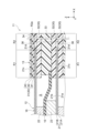
- FIG. 2 is a cross-sectional view taken along line II-II of FIG.
- FIG. 3 is an enlarged cross-sectional view of a portion of FIG.
- FIG. 4 is a cross-sectional view for explaining a method of forming the outer edge welded portion.
- FIG. 5 is an enlarged cross-sectional view showing a part of the power storage module according to the second embodiment.
- FIG. 6 is an enlarged cross-sectional view showing a part of the electricity storage module according to the third embodiment.
- FIG. 7 is a plan view showing a first sealing layer according to a modified example.
- First Embodiment Fig. 1 is a schematic plan view of a power storage module according to a first embodiment.
- the power storage module 11 according to the first embodiment shown in Fig. 1 can be used as a battery for various vehicles such as a forklift, a hybrid vehicle, and an electric vehicle.
- the power storage module 11 is a secondary battery such as a nickel-metal hydride secondary battery or a lithium-ion secondary battery.
- the power storage module 11 may be an electric double layer capacitor or an all-solid-state battery.
- a bipolar lithium-ion secondary battery is exemplified as the power storage module 11.
- FIG. 2 is a cross-sectional view taken along line II-II in FIG. 1, and shows a schematic diagram of the layer structure of the energy storage module 11.
- FIG. 3 is a cross-sectional view showing an enlarged portion of FIG. 2.
- the energy storage module 11 shown in FIGS. 1 to 3 is a single cell having a flattened rectangular parallelepiped shape in the Z-axis direction.
- the energy storage module 11 has a length (length in the X-axis direction) and width (length in the Y-axis direction) of, for example, 100 cm or more. As an example, the length is 150 cm and the width is 120 cm.
- the multiple bipolar electrodes 14 are arranged between the positive electrode terminal electrode 16 and the negative electrode terminal electrode 17 in the stacking direction.
- the bipolar electrodes 14 include a current collector 21, a positive electrode active material layer 22, and a negative electrode active material layer 23.
- the current collector 21 is a chemically inactive electrical conductor that continues to pass current to the positive electrode active material layer 22 and the negative electrode active material layer 23 during discharging or charging of the lithium ion secondary battery.
- the current collector 21 is formed by bonding an aluminum foil 21A and a copper foil 21B together so that the first surface 21a is an aluminum layer and the second surface 21b is a copper layer.
- the current collector 21 may be, for example, a clad foil formed by stacking and rolling-bonding an aluminum foil 21A and a copper foil 21B together.
- the current collector 21 may be a laminated foil. That is, the current collector 21 may be formed by bonding and integrating an aluminum foil 21A and a copper foil 21B together with a conductive adhesive resin (adhesive layer) so that the first surface 21a is an aluminum layer and the second surface 21b is a copper layer.
- the current collector 21 may be formed by copper vapor deposition or copper plating on one side of the aluminum foil so that the first surface 21a is an aluminum layer and the second surface 21b is a copper layer.
- the aluminum layer on the first surface 21a of the current collector 21 may be chromated.
- the copper layer on the second surface 21b of the current collector 21 may be nickel-plated.
- the nickel-plated layer may be a roughened surface that is a protruding plated surface with fine protrusions on the surface.
- the roughened surface may be rougher than the unprocessed metal foil, and may be formed by roughening processing such as etching or electrolytic plating.
- the thickness of the current collector 21 may be about 30 ⁇ m to 150 ⁇ m, but is not limited to this.
- the positive electrode active material layer 22 is provided on the first surface 21a of the current collector 21.
- the current collector 21 and the positive electrode active material layer 22 provided on the first surface 21a of the current collector 21 constitute the positive electrode of the bipolar electrode 14.
- the positive electrode active material layer 22 is formed in a rectangular shape in the center of the first surface 21a so that the peripheral portion 21c of the current collector 21 is exposed.
- the positive electrode active material layer 22 is a layered member including a positive electrode active material, a conductive additive, and a binder.
- the positive electrode active material include a composite oxide, metallic lithium, and sulfur.
- the composition of the composite oxide includes at least one of iron, manganese, titanium, nickel, cobalt, and aluminum, and lithium.
- the composite oxide include olivine-type lithium iron phosphate (LiFePO 4 ), LiCoO 2 , and LiNiMnCoO 2 .
- the positive electrode active material layer 22 may contain a viscosity adjusting solvent such as N-methyl-2-pyrrolidone (NMP).
- NMP N-methyl-2-pyrrolidone
- the negative electrode active material layer 23 is provided on the second surface 21b of the current collector 21.
- the current collector 21 and the negative electrode active material layer 23 provided on the second surface 21b of the current collector 21 constitute the negative electrode of the bipolar electrode 14.
- the negative electrode active material layer 23 is formed in a rectangular shape in the center of the second surface 21b so that the peripheral portion 21c of the current collector 21 is exposed.
- the positive electrode active material layer 22 is contained within the area of the negative electrode active material layer 23 when viewed from the stacking direction. In other words, the outer edge of the positive electrode active material layer 22 is slightly smaller than the outer edge of the negative electrode active material layer 23.
- the negative electrode active material layer 23 is a layered member containing a negative electrode active material, a conductive assistant, and a binder.
- the negative electrode active material include graphite, artificial graphite, highly oriented graphite, mesocarbon microbeads, hard carbon, soft carbon, and other carbon, metal compounds, elements that can be alloyed with lithium or compounds of such elements, boron-added carbon, and the like.
- elements that can be alloyed with lithium include silicon and tin.
- the conductive assistant and binder may be the same as those used in the positive electrode active material layer 22.
- a conventionally known method such as roll coating, die coating, dip coating, doctor blade, spray coating, curtain coating, etc. is used.
- an active material, a solvent, and, if necessary, a binder and a conductive assistant are mixed to produce a slurry-like active material layer forming composition, which is then applied to the first surface 21a and the second surface 21b and then dried.
- the solvent include N-methyl-2-pyrrolidone, methanol, methyl isobutyl ketone, and water. The dried product may be compressed to increase the electrode density.
- the bipolar electrodes 14, 14 adjacent in the stacking direction are arranged so that the positive electrode active material layer 22 of one bipolar electrode 14 faces the negative electrode active material layer 23 of the other bipolar electrode 14.
- a separator 15 is arranged between the bipolar electrodes 14, 14 adjacent in the stacking direction.
- the separator 15 is a sheet-like member having a rectangular shape in a plan view, and prevents short circuits between the bipolar electrodes 14, 14 adjacent in the stacking direction.
- the separator 15 has a rectangular shape that is larger than the positive electrode active material layer 22 and the negative electrode active material layer 23 and smaller than the current collector 21 when viewed from the stacking direction.
- the end 15a of the separator 15 is located outside the positive electrode active material layer 22 and the negative electrode active material layer 23 when viewed from the stacking direction. In other words, the end 15a of the separator 15 does not overlap with either the positive electrode active material layer 22 or the negative electrode active material layer 23 when viewed from the stacking direction.
- Separator 15 is formed by stretching molten resin using a dry process or a wet process.
- separator 15 has a direction in which it shrinks more and a direction in which it shrinks less, depending on the stretching process.
- Separator 15 may be rectangular, with the direction in which it shrinks more along the short sides and the direction in which it shrinks less along the long sides.
- One example of separator 15 is formed by a wet process, with the TD (Transverse Direction) direction in which it shrinks more along the short sides and the MD (Machine Direction) direction in which it shrinks less along the long sides.
- the positive terminal electrode 16 is composed of a current collector 21 and a positive electrode active material layer 22 provided on a first surface 21a of the current collector 21.
- the positive terminal electrode 16 is arranged at one end side in the stacking direction of the electrode laminate 12 so that the positive electrode active material layer 22 on the first surface 21a faces the negative electrode active material layer 23 of the terminal bipolar electrode 14.
- the positive electrode active material layer 22 and the negative electrode active material layer 23 are not provided on the second surface 21b of the current collector 21, and the second surface 21b is electrically connected to an adjacent conductive plate (not shown).
- the current collector 21 used in the positive terminal electrode 16 may be composed of aluminum foil.
- the negative terminal electrode 17 is composed of a current collector 21 and a negative active material layer 23 provided on the second surface 21b of the current collector 21.
- the negative terminal electrode 17 is arranged on the other end side of the electrode laminate 12 in the stacking direction so that the negative active material layer 23 on the second surface 21b faces the positive active material layer 22 of the terminal bipolar electrode 14.
- the positive active material layer 22 and the negative active material layer 23 are not provided on the first surface 21a of the current collector 21, and the first surface 21a is electrically connected to an adjacent conductive plate (not shown).
- the current collector 21 used in the negative terminal electrode 17 may be made of copper foil or a composite material including a copper layer.
- the current collector 21 has an inner surface facing the bipolar electrode 14 and an outer surface facing the opposite side to the inner surface. That is, in the positive terminal electrode 16, the inner surface of the current collector 21 is the first surface 21a, and the outer surface of the current collector 21 is the second surface 21b. On the other hand, in the negative terminal electrode 17, the inner surface of the current collector 21 is the second surface 21b, and the outer surface of the current collector 21 is the first surface 21a.
- the separators 15 described above are arranged between the bipolar electrodes 14, 14 adjacent to each other in the stacking direction, as well as between the bipolar electrodes 14 and the positive terminal electrode 16, and between the bipolar electrodes 14 and the negative terminal electrode 17.
- the arrangement of the separators 15 prevents short circuits between the bipolar electrodes 14 and the positive terminal electrode 16, and between the bipolar electrodes 14 and the negative terminal electrode 17.
- the sealing portion 13 is a member that seals an electrolyte solution (not shown) containing an electrolyte in the internal space S between the collectors 21, 21 adjacent to each other in the stacking direction.
- the sealing portion 13 has electrical insulation properties.
- the sealing portion 13 is provided on the peripheral portion 21c of the collector 21 so as to surround the electrode stack 12 when viewed from the stacking direction.
- the sealing portion 13 is bonded (joined) to the peripheral portion of the collector 21. When viewed from the stacking direction, the sealing portion 13 is spaced apart from the positive electrode active material layer 22 and the negative electrode active material layer 23.
- the sealing portion 13 in one example has a plurality of sealing layers 30, a plurality of spacer layers 33, an end surface welding portion 34, and a plurality of outer edge welding portions 36.
- the plurality of sealing layers 30 and the plurality of spacer layers 33 each have a rectangular frame shape when viewed from the stacking direction.
- the sealing layer 30 and the spacer layer 33 may be formed into a rectangular frame shape by punching or cutting a long sheet material unwound from an original roll.
- the sealing layer 30 and the spacer layer 33 may be formed into a rectangular frame shape by connecting a plurality of sheet materials formed into a rectangular, L-shaped, U-shaped, or other shape.
- the thickness of the sealing layer 30 (length in the stacking direction) may be, for example, 100 ⁇ m or more and 200 ⁇ m or less.
- the thicknesses of the multiple sealing layers 30 may be the same.
- the thickness of the sealing layer 30 adhered to the first surface 21a of the current collector 21 and the thickness of the sealing layer 30 adhered to the second surface 21b may be different from each other.
- the outer edge 21d of the current collector 21 is larger than the inner edge 30a of the seal layer 30 and surrounds the inner edge 30a of the seal layer 30.
- the seal layer 30 and the current collector 21 are joined to each other in the overlapping region when viewed from the stacking direction. That is, the seal layer 30 and the current collector 21 are joined to each other in the region from the inner edge 30a of the seal layer 30 to the outer edge 21d of the current collector 21.
- the inner edge 30a of the seal layer 30 is separated from the positive electrode active material layer 22 and the negative electrode active material layer 23.
- the multiple sealing layers 30 include a pair of first sealing layers 31 and second sealing layers 32.
- the pair of first sealing layers 31 are sealing layers 30 provided on the outer surfaces of the current collectors 21 of the pair of terminal electrodes. That is, one first sealing layer 31 is adhered to the second surface 21b of the positive terminal electrode 16, and the other first sealing layer 31 is adhered to the first surface 21a of the negative terminal electrode 17.
- the pair of first sealing layers 31 are the outermost sealing layers of the multiple sealing layers 30 that are disposed at the stacking ends.
- the second sealing layer 32 is a sealing layer 30 other than the pair of first sealing layers 31, and is disposed between the pair of first sealing layers 31.
- the second sealing layer 32 is provided on the inner surfaces of the current collectors 21 of the pair of terminal electrodes (i.e., the first surface 21a of the current collector 21 of the positive terminal electrode 16 and the second surface 21b of the current collector 21 of the negative terminal electrode 17), and on the first surface 21a and the second surface 21b of the current collector 21 of the bipolar electrode 14.
- the first sealing layer 31 has a multi-layer structure.
- the first sealing layer 31 includes a first resin layer 41, a gas barrier resin layer 42, and a second resin layer 43.
- the first resin layer 41 is welded to the outer surfaces of the current collectors 21 of a pair of terminal electrodes (i.e., the second surface 21b of the positive terminal electrode 16 and the first surface 21a of the negative terminal electrode 17).
- the gas barrier resin layer 42 is provided on the first resin layer 41.
- the second resin layer 43 is provided on the gas barrier resin layer 42 so as to sandwich the gas barrier resin layer 42 between the first resin layer 41 and the second resin layer 43.
- the second resin layer 43 is provided on the gas barrier resin layer 42 and sandwiches the gas barrier resin layer 42 between the second resin layer 43 and the first resin layer 41.
- the first resin layer 41 ensures adhesion between the first sealing layer 31 and the current collector 21, and suppresses peeling of the first sealing layer 31 from the current collector 21.
- the second resin layer 43 covers the gas barrier resin layer 42 and protects the gas barrier resin layer 42 from damage caused by contact with external components.
- the gas barrier resin layer 42 is welded to the first resin layer 41 and the second resin layer 43 so as to overlap the second region R2 when viewed from the stacking direction.
- the gas barrier resin layer 42 is provided at least from the outer edge welded portion 36 to the end face welded portion 34.
- the gas barrier resin layer 42 covers at least the area between the outer edge welded portion 36 and the end face welded portion 34.
- the gas barrier resin layer 42 is provided at least between the outer edge welded portion 36 and the end face welded portion 34.
- the gas barrier resin layer 42 has a lower gas permeability than the first resin layer 41 and the second resin layer 43.
- the gas barrier resin layer 42 is made of a resin material containing vinyl alcohol as a monomer.
- the gas barrier resin layer 42 is made of, for example, ethylene vinyl alcohol copolymer (EVOH) resin or polyvinyl alcohol (PVA) resin.
- EVOH ethylene vinyl alcohol copolymer
- PVA polyvinyl alcohol
- the first resin layer 41, the gas barrier resin layer 42, and the second resin layer 43 may have the same thickness or different thicknesses.
- the second sealing layer 32 (third resin layer) has a single-layer structure and is composed of one resin layer.
- the second sealing layer 32 is welded to the inner surfaces of the current collectors 21 of the pair of terminal electrodes (i.e., the first surface 21a of the current collector 21 of the positive terminal electrode 16 and the second surface 21b of the current collector 21 of the negative terminal electrode 17) and the first surface 21a and the second surface 21b of the current collector 21 of the bipolar electrode 14.
- the second sealing layer 32 is composed of a resin material that is polyolefin resin or modified polyolefin resin and has electrolyte resistance, such as acid-modified PE, acid-modified PP, polyethylene, or polypropylene.
- the second sealing layer 32 is composed of, for example, the same resin material as the first resin layer 41.
- the spacer layer 33 is provided between two sealing layers 30, 30 adjacent to each other in the stacking direction.
- the inner edge 33a of the spacer layer 33 is located in the internal space S formed between the current collectors 21, 21 adjacent to each other in the stacking direction.
- the outer edge 33b of the spacer layer 33 may be in the same position as the outer edge 30b of the sealing layer 30 when viewed from the stacking direction.
- the thickness (length in the stacking direction) of the spacer layer 33 may be thicker than the thickness (length in the stacking direction) of the sealing layer 30, and may be, for example, 200 ⁇ m or more and 500 ⁇ m or less.
- the spacer layer 33 is made of a polyolefin resin or modified polyolefin resin, for example, an electrolyte-resistant resin material such as acid-modified PE, acid-modified PP, polyethylene, or polypropylene.
- the spacer layer 33 has higher crystallinity than the first resin layer 41, the second resin layer 43, and the second seal layer 32. This makes it possible to suppress moisture permeation through the sealing portion 13.
- the first resin layer 41, the second resin layer 43, and the second sealing layer 32 are made of acid-modified PE or acid-modified PP.
- the gas barrier resin layer 42 is made of EVOH resin.
- the spacer layer 33 is made of polyethylene or polypropylene.
- the end surface welded portion 34 is formed by integrating the end portions (outer edge portions) of the plurality of sealing layers 30 and the plurality of spacer layers 33 on the opposite side to the internal space S with each other.
- the sealing layer 30 and the spacer layer 33 are not welded to each other in any part other than the end surface welded portion 34, and are only in contact with each other.
- the end face welded portion 34 is formed by melting the outer edge of the sealing layer 30 and the outer edge of the spacer layer 33 by a heating device such as an infrared heater.
- the thickness of the end surface welded portion 34 is thicker than the first seal layer 31, which is the outermost seal layer, so the end surface welded portion 34 is unlikely to become a permeation path for gas or moisture.
- the outer edge welded portion 36 is provided so as to cover the outer edge 21d of the current collector 21.
- the outer edge welded portion 36 provided on the terminal electrode is formed by integrating the adjacent first resin layers 41 and second seal layers 32 with each other by welding so as to cover the outer edge 21d of the current collector 21 of the terminal electrode.
- the outer edge welded portion 36 provided on the bipolar electrode 14 is formed by integrating the adjacent first resin layers 41, 41 with each other by welding so as to cover the outer edge 21d of the current collector 21 of the bipolar electrode 14.
- the outer edge welded portion 36 When viewed from the stacking direction, the outer edge welded portion 36 is located inside the end face welded portion 34, away from the end face welded portion 34.
- the outer edge welded portion 36 When viewed from the stacking direction, the outer edge welded portion 36 is located outside the outer edge 21d. The outer edge welded portion 36 may or may not be in contact with the outer edge 21d. When viewed from the stacking direction, the outer edge welded portion 36 has a rectangular frame shape that surrounds the electrode stack 12.
- the outer edge welded portion 36 is formed in a similar manner when the current collector 21 is disposed between two second seal layers 32.
- the heating area R by the heating device is limited to the area of the seal layer 30 that overlaps with the current collector 21 and its vicinity. This limits the thickness of the outer edge welded portion 36, thereby making it possible to suppress warping of the current collector 21.
- the sealing portion 13 shown in Figs. 1 to 3 has a communication hole 35 that communicates with each of the multiple internal spaces S.
- the communication hole 35 is formed by partially cutting out the spacer layer 33, and penetrates the spacer layer 33 and the end face welding portion 34.
- the communication hole 35 has one opening in the internal space S and the other opening on the outer surface of the sealing portion 13.
- a cell including one internal space S is formed between adjacent current collectors 21, 21.
- one communication hole 35 is formed for one cell.
- the communication hole 35 can be used as a liquid injection port for injecting electrolyte into the internal space S. That is, a liquid injection port (opening of the communication hole 35) is provided on the outer surface of the sealing portion 13.
- the side on which the communication hole 35 is provided is called the liquid injection port side.
- the inner edge 33a of the spacer layer 33 at the inlet edge is located inside (towards the internal space S) of the inner edge 30a of the seal layer 30.
- the inner edge 33a of the spacer layer 33 at the inlet edge is located, for example, 1 mm or more inside the inner edge 30a and is exposed from the seal layer 30 so as to face the internal space S.
- the inner edge 33a of the spacer layer 33 at a part other than the inlet edge may be located outside the inner edge 30a of the seal layer 30 or may be located inside the inner edge 30a of the seal layer 30.
- the end 15a of the separator 15 is fixed to the seal layer 30 between the seal layer 30 bonded to the second surface 21b of the current collector 21 and the spacer layer 33. It is sufficient that the end 15a of the separator 15 is fixed near the inner edge 30a of the seal layer 30 when viewed from the stacking direction.
- the end 15a may be partially bonded (welded) to the seal layer 30 by, for example, spot welding.
- the sealing layer 30 When viewed from the stacking direction, the sealing layer 30 is spaced apart from the positive electrode active material layer 22 and the negative electrode active material layer 23. When viewed from the stacking direction, the inner edge 30a is located outside the positive electrode active material layer 22 and the negative electrode active material layer 23. When viewed from the stacking direction, the sealing layer 30 adhered to the first surface 21a may overlap with the negative electrode active material layer 23 as long as it is spaced apart from the positive electrode active material layer 22.
- the energy storage module 11 includes an electrode stack 12 and a resin sealing portion 13.
- the sealing portion 13 has a plurality of sealing layers 30 provided on the peripheral portion 21c of the current collector 21, a spacer layer 33 provided between adjacent sealing layers 30, 30 in the stacking direction, and an end face welding portion 34 in which the outer edges of the plurality of sealing layers 30 and the outer edges of the spacer layer 33 are integrated with each other by welding.
- the sealing portion 13 seals the internal space S of the energy storage module 11.
- the thickness of the end face welded portion 34 when viewed from the stacking direction is 1 mm to 5 mm, whereas the thickness in the stacking direction of the outermost sealing layer (first sealing layer 31) located at the end of the stack is thin, at 100 ⁇ m to 200 ⁇ m. Therefore, there is a risk that air may enter the internal space S or the electrolyte in the internal space S may escape to the outside through the first sealing layer 31.
- the energy storage module 11 When manufacturing the energy storage module 11, electrolyte is injected into the internal space S through the communication hole 35 at room temperature (20-25°C), temporarily sealed, and then an activation process is performed. Next, the energy storage module 11 is subjected to an aging process, and then it is vacuum sealed. Finally, the entire energy storage module 11 is laminate-packed with aluminum, which suppresses gas permeation. However, if the energy storage module 11 becomes larger, the first sealing layer 31, which serves as a gas permeation path, also becomes larger, and there is a risk that the amount of gas permeation that occurs before the laminate pack is applied cannot be ignored. In particular, since the aging process is performed at a high temperature of 60°C for a long period of time, such as 80 hours, the amount of gas permeation is likely to increase.
- the first sealing layer 31 includes a first resin layer 41 bonded to the current collector 21, a gas barrier resin layer 42 provided on the first resin layer 41, and a second resin layer 43 provided on the gas barrier resin layer 42.
- the gas barrier resin layer 42 is welded to the first resin layer 41 and the second resin layer 43, and has a lower gas permeability than the first resin layer 41 and the second resin layer 43.
- the gas barrier resin layer 42 can suppress gas permeation through the sealing portion 13. This suppresses a decrease in battery performance.
- the gas barrier resin layer 42 is made of a resin material and has a smaller specific heat than a metal foil such as aluminum, so that the end face welding portion 34 is less likely to be formed poorly. Therefore, it is possible to suppress the deterioration of the sealing property of the sealing portion 13.
- the gas barrier resin layer 42 has a larger number of surface functional groups that contribute to welding with the first resin layer 41 and the second resin layer 43 than a metal foil such as aluminum, so that delamination is less likely to occur than when a metal foil is used.
- the gas barrier resin layer 42 is composed of a resin material containing vinyl alcohol as a monomer.
- Resin materials containing vinyl alcohol as a monomer are capable of compact aggregation between molecules, and are materials with high barrier properties due to the formation of hydrogen bonds between hydrogen groups.
- Resin materials containing vinyl alcohol as a monomer have low gas permeability, so they can reliably suppress gas permeation.
- the first resin layer 41 and the second resin layer 43 are made of the same resin material. Using a common resin material can facilitate the manufacture of the first sealing layer 31.
- the first sealing layer 31 has the same configuration even when inverted in the thickness direction, so the first sealing layer 31 can be used without distinguishing between the front and back. This can further facilitate the manufacture of the energy storage module 11.
- the second sealing layer 32 (third resin layer) bonded to the inner surface of the current collector 21 of the terminal electrode (i.e., the first surface 21a of the current collector 21 of the positive terminal electrode 16 and the second surface 21b of the current collector 21 of the negative terminal electrode 17) is made of the same resin material as the first resin layer 41.
- the first sealing layer 31 and the second sealing layer 32 can be manufactured more easily.
- the sealing portion 13 has an outer edge welded portion 36 in which the first resin layer 41 and the second seal layer 32 are integrated with each other by welding so as to cover the outer edge 21d of the current collector 21.
- the outer edge welded portion 36 can prevent the first resin layer 41 and the second seal layer 32 from peeling off from the current collector 21.
- the first resin layer 41 and the second seal layer 32 are made of the same resin material, and therefore are easily compatible with each other. Therefore, the outer edge welded portion 36 is easy to form.
- the outer edge welded portion 36 When viewed from the stacking direction, the outer edge welded portion 36 is disposed at a distance from the end surface welded portion 34. Between the outer edge welded portion 36 and the end surface welded portion 34, the first seal layer 31 and the second seal layer 32 are not welded to each other. As such, the first seal layer 31 and the second seal layer 32 have portions that are not welded to each other, so warping of the current collector 21 can be suppressed.
- Second Embodiment 5 is a cross-sectional view showing an enlarged portion of the storage module according to the second embodiment.
- the storage module 11A according to the second embodiment shown in FIG. 5 differs from the storage module 11 in that the second seal layer 32 has a multi-layer structure.
- the second seal layer 32 includes a third resin layer 44, a core resin layer 45, and a fourth resin layer 46.
- the third resin layer 44 is bonded to the inner surfaces of the current collectors 21 of the pair of terminal electrodes (i.e., the first surface 21a of the current collector 21 of the positive terminal electrode 16 and the second surface 21b of the current collector 21 of the negative terminal electrode 17), and the first surface 21a and the second surface 21b of the current collector 21 of the bipolar electrode 14.
- the core resin layer 45 is provided on the third resin layer 44.
- the fourth resin layer 46 is provided on the core resin layer 45 so as to sandwich the core resin layer 45 between the third resin layer 44 and the fourth resin layer 46.
- the fourth resin layer 46 is in contact with the spacer layer 33.
- the third resin layer 44 and the fourth resin layer 46 ensure adhesion between the second seal layer 32 and the current collector 21 , and thus peeling of the second seal layer 32 from the current collector 21 is suppressed.
- the third resin layer 44 and the fourth resin layer 46 are, for example, made of the same resin material.
- the third resin layer 44 and the fourth resin layer 46 may be made of the same resin material as the second seal layer 32 of the energy storage module 11.
- the third resin layer 44 and the fourth resin layer 46 are made of a polyolefin resin or a modified polyolefin resin, for example, an electrolyte-resistant resin material such as acid-modified PE, acid-modified PP, polyethylene, or polypropylene.
- the resin materials making up the third resin layer 44 and the fourth resin layer 46 may be different from each other.
- the first resin layer 41, the second resin layer 43, the third resin layer 44, and the fourth resin layer 46 may be, for example, made of the same resin material.
- the core resin layer 45 is welded to the third resin layer 44 and the fourth resin layer 46.
- the core resin layer 45 is made of a polyolefin resin or modified polyolefin resin, for example, an electrolyte-resistant resin material such as acid-modified PE, acid-modified PP, polyethylene, or polypropylene.
- the core resin layer 45 has higher crystallinity than the third resin layer 44 and the fourth resin layer 46.
- the core resin layer 45 is made of, for example, the same material as the spacer layer 33.
- the first resin layer 41, the second resin layer 43, the third resin layer 44, and the fourth resin layer 46 are formed from acid-modified PE or acid-modified PP.
- the gas barrier resin layer 42 is formed from EVOH resin.
- the spacer layer 33 and the core resin layer 45 are formed from polyethylene or polypropylene.
- the first sealing layer 31 includes a gas barrier resin layer 42, so that gas permeation through the sealing portion 13 can be suppressed in the same manner as in the energy storage module 11.
- the second sealing layer 32 includes a third resin layer 44 that is made of the same resin material as the first resin layer 41 and is bonded to the inner surface of the terminal electrode (i.e., the first surface 21a of the current collector 21 of the positive terminal electrode 16 and the second surface 21b of the current collector 21 of the negative terminal electrode 17).
- the outer edge welded portion 36 is formed by integrating the first resin layer 41 of the first sealing layer 31 and the third resin layer 44 of the second sealing layer 32 by welding.
- the second sealing layer 32 includes a core resin layer 45 that has higher crystallinity than the first resin layer 41.
- the core resin layer 45 together with the spacer layer 33, suppresses moisture permeation through the sealing portion 13 and improves gas barrier properties.
- Third Embodiment Fig. 6 is an enlarged cross-sectional view showing a part of the power storage module according to the third embodiment.
- the gas barrier resin layer 42 is thicker than the first resin layer 41 and the second resin layer 43.
- the thickness of the gas barrier resin layer 42 may be 50% or more, 60% or more, or 70% or more of the total thickness of the seal layer 30.
- the gas barrier resin layer 42 is thick, so that in the airtightness test between the cell and the outside that is performed during manufacturing, the test gas injected into the internal space S from the communication hole 35 is prevented from permeating the first seal layer 31 and leaking to the outside.
- the test gas may be a rare gas such as argon, an inert gas such as nitrogen, or hydrogen, ammonia, or a halogen gas.
- a detection sensor disposed outside the energy storage module 11B detects whether or not the detection gas is leaking. If the detection sensor does not detect the test gas, it is determined that there is no problem with the airtightness between the cell and the outside.
- the thickness of the first sealing layer 31, which is the outermost sealing layer, is thinner than the thickness of the end face welding portion 34, so there is a risk that the test gas will leak from the internal space S through the first sealing layer 31.
- the gas barrier resin layer 42 suppresses the permeation of the test gas, so it is possible to reliably detect any problem with the airtightness between the cell and the outside, i.e., any leakage of the test gas through the end face welding portion 34.
- EVOH resin which is an example of a resin used in the gas barrier resin layer 42, has higher resin strength than acid-modified PE, which is an example of a resin used in the first resin layer 41 and the second resin layer 43. This makes it possible to improve the pressure resistance strength of the energy storage module 11B.
- the gas barrier resin layer 42 is, for example, an EVOH resin with an ethylene ratio of 30% or less.
- One example of the gas barrier resin layer 42 is an EVOH resin with an ethylene ratio of 27%.
- the first resin layer 41 and the second resin layer 43 have, for example, the same thickness.
- the thickness of the first resin layer 41 and the second resin layer 43 is, for example, 20 ⁇ m or more. This ensures adhesion.
- An example of the thickness of the first resin layer 41 and the second resin layer 43 is 30 ⁇ m.
- FIG. 7 is a plan view showing a first sealing layer according to a modified example.
- the first sealing layer 31A according to the modified example is formed by connecting a plurality of sheet materials 60.
- four rectangular sheet materials 60 are connected to form the first sealing layer 31A.
- the first sealing layer 31A includes a connecting portion 61 in which two sheet materials 60 are overlapped and connected.
- the connecting portion 61 at least a portion of the ends of the two sheet materials 60 are arranged overlapping each other.
- the first resin layer 41 and the second resin layer 43 are made of polyolefin resin or modified polyolefin resin. This makes it easier for the sheet materials 60 to be welded together at the connecting portion 61.
- At least one first sealing layer 31 may include a gas barrier resin layer 42, and the other first sealing layer 31 may have the same configuration as the second sealing layer 32.
- the above embodiments and modifications may be combined as appropriate.
- the gas barrier resin layer is composed of a resin material containing vinyl alcohol as a monomer.
- the first seal layer is formed by connecting a plurality of sheet materials and includes a connecting portion in which the first resin layer and the second resin layer of two of the sheet materials are overlapped and welded to each other, In the connecting portion, the first resin layer and the second resin layer are made of a polyolefin resin.
- the storage module according to [1] or [2].
- the first resin layer is a polyolefin resin
- the plurality of sealing layers further includes a second sealing layer provided on the inner surface, the second seal layer includes a third resin layer made of a polyolefin resin and welded to the inner surface;
- the sealing portion further includes an outer edge welded portion in which the first resin layer and the third resin layer are integrated with each other by welding so as to cover an outer edge of the current collector.
- the storage module according to any one of [1] to [3].
- the outer edge welded portion is disposed at a distance from the end surface welded portion, the gas barrier resin layer is provided at least between the outer edge welded portion and the end surface welded portion when viewed from the stacking direction.
- the second seal layer is provided on the third resin layer and further includes a core resin layer having higher crystallinity than the third resin layer.
Landscapes
- Chemical & Material Sciences (AREA)
- Chemical Kinetics & Catalysis (AREA)
- Electrochemistry (AREA)
- General Chemical & Material Sciences (AREA)
- Engineering & Computer Science (AREA)
- Manufacturing & Machinery (AREA)
- Power Engineering (AREA)
- Physics & Mathematics (AREA)
- Condensed Matter Physics & Semiconductors (AREA)
- General Physics & Mathematics (AREA)
- Inorganic Chemistry (AREA)
- Microelectronics & Electronic Packaging (AREA)
- Dispersion Chemistry (AREA)
- Sealing Battery Cases Or Jackets (AREA)
- Electric Double-Layer Capacitors Or The Like (AREA)
Priority Applications (4)
| Application Number | Priority Date | Filing Date | Title |
|---|---|---|---|
| JP2025542901A JPWO2025047414A1 (https=) | 2023-09-01 | 2024-08-13 | |
| EP24859450.9A EP4734249A1 (en) | 2023-09-01 | 2024-08-13 | Power storage module |
| CN202480055135.XA CN121729788A (zh) | 2023-09-01 | 2024-08-13 | 蓄电模块 |
| KR1020267005064A KR20260040637A (ko) | 2023-09-01 | 2024-08-13 | 축전 모듈 |
Applications Claiming Priority (2)
| Application Number | Priority Date | Filing Date | Title |
|---|---|---|---|
| JP2023142123 | 2023-09-01 | ||
| JP2023-142123 | 2023-09-01 |
Publications (1)
| Publication Number | Publication Date |
|---|---|
| WO2025047414A1 true WO2025047414A1 (ja) | 2025-03-06 |
Family
ID=94819290
Family Applications (1)
| Application Number | Title | Priority Date | Filing Date |
|---|---|---|---|
| PCT/JP2024/028900 Pending WO2025047414A1 (ja) | 2023-09-01 | 2024-08-13 | 蓄電モジュール |
Country Status (5)
| Country | Link |
|---|---|
| EP (1) | EP4734249A1 (https=) |
| JP (1) | JPWO2025047414A1 (https=) |
| KR (1) | KR20260040637A (https=) |
| CN (1) | CN121729788A (https=) |
| WO (1) | WO2025047414A1 (https=) |
Citations (4)
| Publication number | Priority date | Publication date | Assignee | Title |
|---|---|---|---|---|
| JP2623311B2 (ja) | 1988-09-01 | 1997-06-25 | 古河電池株式会社 | バイポーラ電池用極板の製造法 |
| JP2020135935A (ja) * | 2019-02-13 | 2020-08-31 | 株式会社豊田自動織機 | 電極ユニット及び蓄電モジュール |
| WO2022244853A1 (ja) * | 2021-05-19 | 2022-11-24 | 大日本印刷株式会社 | 蓄電デバイスの非透水性ガス抜きフィルム |
| WO2023120171A1 (ja) * | 2021-12-21 | 2023-06-29 | 株式会社豊田自動織機 | 蓄電装置 |
-
2024
- 2024-08-13 JP JP2025542901A patent/JPWO2025047414A1/ja active Pending
- 2024-08-13 WO PCT/JP2024/028900 patent/WO2025047414A1/ja active Pending
- 2024-08-13 CN CN202480055135.XA patent/CN121729788A/zh active Pending
- 2024-08-13 EP EP24859450.9A patent/EP4734249A1/en active Pending
- 2024-08-13 KR KR1020267005064A patent/KR20260040637A/ko active Pending
Patent Citations (4)
| Publication number | Priority date | Publication date | Assignee | Title |
|---|---|---|---|---|
| JP2623311B2 (ja) | 1988-09-01 | 1997-06-25 | 古河電池株式会社 | バイポーラ電池用極板の製造法 |
| JP2020135935A (ja) * | 2019-02-13 | 2020-08-31 | 株式会社豊田自動織機 | 電極ユニット及び蓄電モジュール |
| WO2022244853A1 (ja) * | 2021-05-19 | 2022-11-24 | 大日本印刷株式会社 | 蓄電デバイスの非透水性ガス抜きフィルム |
| WO2023120171A1 (ja) * | 2021-12-21 | 2023-06-29 | 株式会社豊田自動織機 | 蓄電装置 |
Also Published As
| Publication number | Publication date |
|---|---|
| EP4734249A1 (en) | 2026-04-29 |
| JPWO2025047414A1 (https=) | 2025-03-06 |
| CN121729788A (zh) | 2026-03-24 |
| KR20260040637A (ko) | 2026-03-25 |
Similar Documents
| Publication | Publication Date | Title |
|---|---|---|
| CN101320823B (zh) | 二次电池及其制造方法 | |
| JP7334693B2 (ja) | 蓄電装置 | |
| JP2023087348A (ja) | 蓄電装置の製造方法及び蓄電装置 | |
| KR20140012601A (ko) | 이차전지 및 이를 포함하는 전기화학소자 | |
| JP7468233B2 (ja) | 蓄電モジュール | |
| KR20160141654A (ko) | 리튬 이온 2차 전지 | |
| JP7559840B2 (ja) | 蓄電セル及び蓄電装置 | |
| WO2023145294A1 (ja) | 蓄電モジュール | |
| JP7459758B2 (ja) | 蓄電セル | |
| JP7722249B2 (ja) | 蓄電装置 | |
| WO2024062824A1 (ja) | 蓄電モジュール及び蓄電装置 | |
| WO2023120171A1 (ja) | 蓄電装置 | |
| WO2025047414A1 (ja) | 蓄電モジュール | |
| US20250219206A1 (en) | Power storage module and manufacturing method of power storage module | |
| US20040224226A1 (en) | Electrochemical cell and production method therefor | |
| CN114914518B (zh) | 非水电解液二次电池 | |
| KR20140000489A (ko) | 이차전지 및 그 제조방법, 이를 포함하는 중대형 전지모듈 | |
| JP7489004B2 (ja) | 蓄電セル及び蓄電装置 | |
| JP7444029B2 (ja) | 蓄電セル及び蓄電装置 | |
| WO2025115754A1 (ja) | 蓄電モジュールの製造方法及び蓄電モジュール | |
| JP2025051097A (ja) | 蓄電装置の製造方法 | |
| WO2024034403A1 (ja) | 蓄電モジュール | |
| JP2024162813A (ja) | 蓄電モジュール | |
| JP2024080295A (ja) | 蓄電装置 | |
| KR20240151800A (ko) | 축전 장치 |
Legal Events
| Date | Code | Title | Description |
|---|---|---|---|
| 121 | Ep: the epo has been informed by wipo that ep was designated in this application |
Ref document number: 24859450 Country of ref document: EP Kind code of ref document: A1 |
|
| ENP | Entry into the national phase |
Ref document number: 2025542901 Country of ref document: JP Kind code of ref document: A |
|
| WWE | Wipo information: entry into national phase |
Ref document number: 2025542901 Country of ref document: JP |
|
| WWE | Wipo information: entry into national phase |
Ref document number: 2024859450 Country of ref document: EP |
|
| ENP | Entry into the national phase |
Ref document number: 2024859450 Country of ref document: EP Effective date: 20260122 |
|
| ENP | Entry into the national phase |
Ref document number: 2024859450 Country of ref document: EP Effective date: 20260122 |
|
| ENP | Entry into the national phase |
Ref document number: 1020267005064 Country of ref document: KR Free format text: ST27 STATUS EVENT CODE: A-0-1-A10-A15-NAP-PA0105 (AS PROVIDED BY THE NATIONAL OFFICE) |
|
| WWE | Wipo information: entry into national phase |
Ref document number: 1020267005064 Country of ref document: KR |
|
| WWP | Wipo information: published in national office |
Ref document number: 1020267005064 Country of ref document: KR |