WO2025041274A1 - マイクロ波反応炉 - Google Patents
マイクロ波反応炉 Download PDFInfo
- Publication number
- WO2025041274A1 WO2025041274A1 PCT/JP2023/030188 JP2023030188W WO2025041274A1 WO 2025041274 A1 WO2025041274 A1 WO 2025041274A1 JP 2023030188 W JP2023030188 W JP 2023030188W WO 2025041274 A1 WO2025041274 A1 WO 2025041274A1
- Authority
- WO
- WIPO (PCT)
- Prior art keywords
- microwave
- reactor
- opening
- microwaves
- reflected wave
- Prior art date
- Legal status (The legal status is an assumption and is not a legal conclusion. Google has not performed a legal analysis and makes no representation as to the accuracy of the status listed.)
- Pending
Links
Images


Classifications
-
- B—PERFORMING OPERATIONS; TRANSPORTING
- B01—PHYSICAL OR CHEMICAL PROCESSES OR APPARATUS IN GENERAL
- B01J—CHEMICAL OR PHYSICAL PROCESSES, e.g. CATALYSIS OR COLLOID CHEMISTRY; THEIR RELEVANT APPARATUS
- B01J19/00—Chemical, physical or physico-chemical processes in general; Their relevant apparatus
- B01J19/08—Processes employing the direct application of electric or wave energy, or particle radiation; Apparatus therefor
- B01J19/12—Processes employing the direct application of electric or wave energy, or particle radiation; Apparatus therefor employing electromagnetic waves
Definitions
- This disclosure relates to microwave reactors.
- microwaves are supplied to the inside of the reactor through a waveguide. Because the opening area of the waveguide is small, few microwaves are reflected back to the waveguide. The current flowing through the conductor in the tube wall heats the waveguide, and losses also occur in the waveguide. However, if the reactor is not large-scale, microwaves of a few kW level are sufficient, so the heat and loss generated in the waveguide are at an acceptable level. On the other hand, in large-scale plants, microwaves of high power, such as hundreds of kW to tens of MW, must be supplied, so the heat and loss generated in the waveguide cannot be ignored.
- the waveguide WRI-26 is a narrow tube with a cross-section of 8.4 cm x 4.2 cm. As a result, the wall currents generated when 1 MW microwaves propagate through the tube are concentrated in an extremely small area of no more than 8 cm, resulting in a large amount of heat and loss.
- microwaves were generated by an oscillator using a magnetron.
- magnetrons have poor frequency purity and phase stability, making it difficult to synthesize microwaves from multiple magnetrons.
- the microwaves that can be generated by a single magnetron are limited to 10 kW or less at 2.45 GHz, for example, making it difficult to generate high-power microwaves exceeding 10 kW.
- the efficiency drops to 60% or less at high powers such as 10 kW, making it impossible to generate high-power, highly efficient microwaves.
- a device has been proposed in which an antenna is installed inside a reactor without using a waveguide (see, for example, Patent Document 1).
- microwaves reflected by the inner wall of the reactor may return directly to the antenna, destroying equipment such as the amplifier that supplies the microwaves to the antenna. For this reason, an isolator is provided between the amplifier output and the antenna to prevent reflected waves.
- the isolator becomes large and difficult to place, and isolators are expensive. For example, when irradiating high-power microwaves of more than 10 kW at 2.45 GHz, the reflected waves can destroy equipment, which can be a problem.
- This disclosure has been made to solve the problems described above, and its purpose is to obtain a microwave reactor that can suppress damage to equipment caused by reflected waves even when high-power microwaves are irradiated.
- the microwave reactor comprises a reactor for storing reactants and a microwave generator for generating a microwave beam, the reactor being provided with an opening, the microwave generator concentrating the microwave beam at the center of the opening and directing the microwave beam into the interior of the reactor, the inner wall of the reactor reflecting the microwave beam, the dimension of the opening being longer than half the wavelength of the microwave beam, and the area of the opening being 1/10 or less of the area of the portion of the inner wall of the reactor that is not covered by the reactants.
- the area of the reactor opening is set to 1/10 or less of the area of the portion of the reactor's inner wall that is not covered by the reactant. This makes it possible to prevent damage to equipment caused by reflected waves even when high-power microwaves are irradiated.
- FIG. 1 is a cross-sectional view showing a microwave reactor according to a first embodiment.
- FIG. 11 is a cross-sectional view showing a microwave reactor according to a second embodiment.
- FIG. 13 is a diagram showing the calculation results of spatially combining microwaves from a rectangular array antenna.
- FIG. 13 is a diagram showing the calculation results of spatially combining microwaves from a rectangular array antenna.
- FIG. 1 illustrates a circular array antenna.
- FIG. 13 is a diagram showing the calculation results of spatially combining microwaves from a circular array antenna.
- FIG. 13 is a diagram showing the calculation results of spatially combining microwaves from a circular array antenna.
- FIG. 11 is a circuit diagram of an oscillator of a microwave reactor according to a third embodiment.
- FIG. 11 is a circuit diagram of an oscillator according to a comparative example.
- FIG. 11 is a cross-sectional view showing a microwave reactor according to a fourth embodiment.
- FIG. 13 is a cross-sectional view showing a microwave reactor according to a fifth embodiment.
- FIG. 13 is a cross-sectional view showing a microwave reactor according to a sixth embodiment.
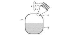
- Embodiment 1. 1 is a cross-sectional view showing a microwave reactor according to the first embodiment.
- the reactor 1 contains a reactant 2.
- the inner wall of the lower part of the reactor 1 is covered with the reactant 2.
- An opening 3 is provided in the upper part of the reactor 1 that is not covered with the reactant 2.
- a microwave generator 4 generates a microwave beam 5 that is an electromagnetic microwave wave.
- the microwave has a frequency of 0.9 GHz to 30 GHz and a wavelength of 33 cm to 1 cm.
- the microwave generator 4 is, for example, a horn antenna, and emits a microwave beam 5 into the inside of the reactor 1 through the opening 3.
- the microwaves that enter the inside of the reactor 1 are absorbed by the reactant 2, and the microwaves cause reactions such as chemical reactions, sintering, and drying of the reactant 2.
- microwaves are injected into a reactor through a waveguide, and because higher modes increase loss, the diameter of the waveguide is set to half the wavelength or less.
- the microwave generator 4 directly injects the microwave beam 5 into the inside of the reactor 1 without using a waveguide, so the dimensions of the opening 3 can be made larger than half the wavelength of the microwave beam 5.
- the microwave generator 4 focuses the microwave beam 5 on the center of the opening 3 and causes the microwave beam to enter the inside of the reactor 1. As a result, almost no microwaves are irradiated onto the end of the opening 3, so no current flows at the edge of the opening 3, suppressing the heat generation and microwave loss in the power supply area that were problems when using a waveguide.
- the reactor 1 is made of a metal such as stainless steel, the upper inner wall of the reactor 1 that is not covered by the reactant 2 reflects the microwave beam 5. Inside the reactor 1, the microwave beam 5 is multiple-reflected, and is repeatedly absorbed and reflected by the reactant 2. As a result, the reactant 2 inside the reactor 1 can be irradiated with the microwave beam 5 relatively uniformly.
- the microwave beam 5 is almost totally reflected by the inner wall of the reactor 1, and the inside of the reactor 1 has an electromagnetic field distribution resonating due to multiple reflections. If a small opening 3 is opened in the reactor 1 in this state, it becomes a state similar to so-called blackbody radiation. Of such microwaves, the reflected waves that go out from the opening 3 are a weak amount proportional to the ratio of the area of the upper inner wall of the reactor 1 that is not covered by the reactant 2 to the surface area of the opening 3. If there are many reflected waves, the amount of microwaves that reach the reactant 2 decreases, and the efficiency of the furnace decreases. In addition, there is a risk that the reflected waves will destroy the microwave generator 4.
- the amount of reflected waves needs to be suppressed to a very small amount, less than one-tenth of the microwaves inside the reactor 1.
- Embodiment 2. 2 is a cross-sectional view showing a microwave reactor according to embodiment 2.
- the microwave generator 4 has a chamber 6, a plurality of antennas 7, and a plurality of oscillators 8.
- the chamber 6 is connected to the opening 3 of the reactor 1, and surrounds a space for forming the microwave beam 5.
- the chamber 6 is made of a conductor such as a metal so as to prevent microwaves due to unnecessary side lobes generated by the microwave beam from leaking to the outside.
- the multiple antennas 7 are provided on the walls of the chamber 6, and spatially combine the microwave beams 5 inside the chamber 6.
- the multiple oscillators 8 supply phase-controlled microwave electrical signals to the multiple antennas 7, respectively.
- Each oscillator 8 has an oscillation source and a semiconductor amplifier such as GaN.
- Magnetrons generally have unstable phases and a wide frequency bandwidth. For this reason, when microwaves supplied from two or more magnetrons are combined, the combined power and efficiency drop significantly due to combination losses.
- the spacing between the antennas 7 is approximately half the wavelength, so at 2.45 GHz it is approximately 6 cm. Therefore, the size of the array antenna is approximately 60 cm x 60 cm, which is a size that is easily feasible.
- the microwave power can be increased by spatially combining the number of array antennas, so even microwaves of 30 kW or more can be easily realized. For example, if an output of 1 MW is required at 2.45 GHz, 3,333 300 W oscillators can be spatially combined. If the antennas 7 are arranged in a square, there will be approximately 58 x 58, and if they are spaced ⁇ /2 apart, each side will be approximately 3.4 m, which is easily feasible in a large furnace.
- Figure 5 shows a circular array antenna. Multiple antennas 7 are arranged in a circular area at intervals of approximately half a wavelength. The number of antennas is 363, which is almost the same as the number of antennas in the rectangular array described above. The circular array can concentrate microwaves more in the center of the aperture 3 than the rectangular array.
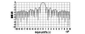
- Figures 6 and 7 show the calculation results of spatially combining microwaves from a circular array antenna.
- the diameter of the circular array is about 64 cm, which is equivalent to that of a square array.
- Figure 6 shows the microwave amplitude in dB on a plane 4.5 ⁇ away from the antenna.
- Figure 7 shows the cumulative power ratio accumulated according to the distance d from the center in units of 10%.
- the amplitude of the side lobe of the circular array is reduced compared to the square array in Figure 3.
- the proportion of microwaves passing through the aperture 3 with a radius of 10 ⁇ has increased to 86%. This shows that the circular array is superior to the square array in radiating more power to the aperture 3. Note that this calculation does not include the component reflected by the side wall of the chamber 6 and reaching the aperture 3, so in reality it is possible to pass an even greater proportion of the microwaves through the aperture 3.
- Embodiment 3. 8 is a circuit diagram of an oscillator of a microwave reactor according to the third embodiment.
- the oscillator 8 has an oscillation source 9, an amplifier 10 including at least one stage of a transistor, and a reflected wave monitor circuit 12 connected between a final stage transistor 11 of the amplifier 10 and an antenna 7.
- the oscillation source 9 generates a microwave electric signal.
- the amplifier 10 amplifies the microwave electric signal from the oscillation source 9.
- the final stage transistor 11 of the amplifier 10 is a GaN transistor.
- the electric signal amplified by the GaN transistor is supplied to the antenna 7.
- the antenna 7 radiates microwaves.
- the drain voltage control circuit 13 controls the drain voltage of the final stage transistor 11.
- the gate voltage control circuit 14 controls the gate voltage of the final stage transistor 11.
- the reflected wave monitor circuit 12 monitors the intensity of the reflected wave returning from the antenna 7.
- the reflected wave monitor circuit 12 is configured, for example, by a circuit such as a directional coupler connected to a detection diode.
- the reflected wave monitor circuit 12 controls the drain voltage control circuit 13 to quickly lower the drain voltage of the final stage transistor 11 to 0 V or a low voltage, or controls the gate voltage control circuit 14 to lower the operating current of the final stage transistor 11.
- the threshold of the strength of the reflected wave for performing such control is, for example, 1/2 to several times the strength of the output signal of the oscillator 8.
- FIG. 9 is a circuit diagram of an oscillator according to the comparative example.
- an isolator 15 is connected between an LDMOS transistor 16, which is the final stage transistor of the amplifier 10, and an antenna 7.
- the area of the opening 3 of the reactor 1 is set to 1/10 or less of the area of the part of the inner wall of the reactor 1 that is not covered by the reactant 2, so that the reflected wave from the reactor 1 is suppressed.
- a large reflected wave may enter the antenna 7 due to an unexpected sudden event such as not filling the reactant 2.
- Such an excessive signal may damage the final stage transistor 11 of the oscillator 8.
- an isolator 15 is provided in the comparative example.
- the isolator 15 is a magnetic circuit, and if the output is increased to 300 W, it becomes large and expensive.
- the isolator 15 has a built-in resistor that converts the reflected wave into heat.
- the resistor is also large in size to handle large power.
- the reflected power is large, the resistor may burn out. Therefore, the isolator 15 must be replaced to restore operation, which takes a lot of time and costs.
- a reflected wave monitor circuit 12 is provided between the final stage transistor 11 of the amplifier 10 and the antenna 7.
- the reflected wave monitor circuit 12 controls the drain voltage or operating current of the final stage transistor 11 to be lowered. This makes it possible to prevent the amplifier 10 connected to the antenna 7 from being destroyed even if a large reflected wave occurs. Also, because only the drain voltage or operating current of the final stage transistor 11 is changed, recovery can be achieved by simply restoring both voltages to their original state. Therefore, recovery can be achieved in a short time without the need to replace parts.
- a reflected wave monitor circuit 12 is provided for each antenna 7.
- one reflected wave monitor circuit 12 may be provided for multiple antennas 7, and when a reflected wave arrives from an antenna 7, the drain voltage or operating current of all the final stage transistors 11 of multiple oscillators 8 may be controlled to be lowered.
- a reflected wave monitor circuit 12 may be provided for one oscillator 8 in a block of 10 or 25 antennas 7, and all the final stage transistors 11 in the same block may be controlled collectively to be lowered in drain voltage or operating current. By controlling multiple antennas collectively, the number of control devices can be reduced, thereby reducing costs.
- a microwave reactor is not a free space but a closed space, and the direction of the microwave beam is fixed. For this reason, unlike array antennas such as those used in general radars, there is no possibility of a reflection from the outside hitting just one specific unit, and the reflected wave hits the entire reactor. Therefore, even a protection circuit for each block like this is effective.
- the final stage transistor 11 of the amplifier 10 is a GaN transistor.
- GaN transistors are more efficient than conventional LDMOS transistors, and therefore can improve the energy efficiency of the microwave reactor. Furthermore, GaN transistors have a higher voltage resistance than LDMOS transistors and are less likely to be damaged even when high voltages are applied, and therefore have a high resistance to reflected waves.
- Embodiment 4. 10 is a cross-sectional view showing a microwave reactor according to embodiment 4.
- a plurality of openings 3 are provided in the reactor 1.
- a plurality of microwave generators 4 focus microwave beams 5 on the centers of the plurality of openings 3, respectively, and cause the microwave beams 5 to enter the inside of the reactor 1. Note that, although the figure shows two openings 3 and two microwave generators 4, the number is not limited thereto, and three or more may be used.
- each opening 3 are longer than half the wavelength of the microwave beam 5, and the area of each opening 3 is 1/10 or less of the area of the portion of the inner wall of the reactor 1 that is not covered by the reactant 2.
- Multiple openings 3 are arranged so that the microwaves incident from each opening 3 do not enter directly into other openings 3 without being reflected by the inner wall of the reactor 1.
- the reactor 1 When the reactor 1 is large or the microwave power is very high, multiple microwaves are supplied into the reactor 1 from multiple openings 3 as described above. However, because the reactor 1 is large, the electromagnetic field distribution becomes uneven due to multiple reflections inside the reactor. As a result, the microwaves irradiated to the reactant 2 are not homogeneous, and the reaction does not proceed uniformly, resulting in a decrease in yield or deterioration of reaction efficiency.
- Microwaves entering the closed space inside the reactor 1 from each opening 3 are reflected multiple times, generating standing electromagnetic waves with peaks and valleys.
- the peaks and valleys of the standing waves can be changed by changing the phase of the microwaves.
- the oscillator 8 is an oscillator that uses semiconductors such as GaN, it is possible to precisely control the phase of the microwaves.
- the oscillators 8 of the multiple microwave generators 4 each control the phase of the microwaves incident from the multiple openings 3 so that the microwave distribution (electromagnetic field distribution) inside the reactor 1 is uniform. This allows the microwaves to be uniformly irradiated onto the reactants 2 inside the reactor, making the reaction of the reactants 2 uniform.
- the optimal phase control can be determined by performing a simulation in advance, or the phase can be changed to set conditions that provide good yields.
- Embodiment 5. 11 is a cross-sectional view showing a microwave reactor according to embodiment 5.
- the reactor 1 is surrounded by an explosion-proof wall 17 to contain gas generated from the reactor 1. Since the oscillator 8 is provided outside the explosion-proof wall 17, the oscillator 8 does not need to be explosion-proof and can be manufactured at low cost.
- a shielding plate 18 is provided at the opening 3 of the reactor 1.
- the shielding plate 18 prevents the material inside the reactor 1 from escaping from the opening 3 to the outside of the reactor 1. Therefore, the material generated inside the reactor 1 does not adhere to the antenna 7 of the microwave generator 4, preventing deterioration of the antenna 7.
- the microwave beam 5 can pass through the shielding plate 18.
- the shielding plate 18 is a quartz plate with a thickness of half the wavelength of the microwave beam 5.
- the microwaves passing through the shielding plate 18 are reflected by the upper and lower surfaces of the shielding plate 18, but the reflected waves from the upper and lower surfaces of the shielding plate 18 cancel each other out. This makes it possible to suppress a decrease in the amount of microwave power supply due to unnecessary reflections.
- the shielding plate 18 is not limited to a quartz plate, but may be any dielectric plate such as glass or resin that allows microwaves to pass through, or may be a dielectric plate made of a fibrous material. Also, the shielding plate 18 is not limited to a single dielectric plate, but may be multiple dielectric plates.
- the dielectric loss of the quartz plate Since this heat generation is caused by the dielectric loss of the quartz plate, the dielectric loss can be reduced by making the plate thickness of the quartz plate sufficiently thinner than the half wavelength. However, there is a risk that the quartz thin film may be damaged due to the pressure difference between the inside and outside of the reactor.
- the shielding plate 18 has two dielectric thin films 19, 20 and a honeycomb material 21 sandwiched between the two dielectric thin films 19, 20 and having a thickness of 1/4 wavelength of the microwave beam 5.
- the dielectric thin films 19, 20 are quartz thin films with a plate thickness that is sufficiently thinner than half the wavelength. Therefore, unnecessary heat generation can be suppressed.
- the honeycomb material 21 is a dielectric with a relative dielectric constant close to 1 that has little effect on microwaves, such as glass fiber reinforced plastic.
- the honeycomb material 21 By arranging the two dielectric thin films 19, 20 1/4 wavelength apart, the reflected waves can be cancelled out. This makes it possible to suppress a decrease in the amount of microwave power supply due to unnecessary reflections.
- the quartz thin film can be strengthened to support the pressure received from the reactor 1.
- the dielectric thin films 19 and 20 are not limited to quartz thin films, but may be made of glass, resin, or other dielectric thin films that are permeable to microwaves, and may also be made of a fibrous material. Also, the dielectric thin films 19 and 20 do not have to consist of two thin films, but may consist of multiple thin films.
Landscapes
- Chemical & Material Sciences (AREA)
- Physics & Mathematics (AREA)
- Electromagnetism (AREA)
- Health & Medical Sciences (AREA)
- General Health & Medical Sciences (AREA)
- Toxicology (AREA)
- Organic Chemistry (AREA)
- Chemical Kinetics & Catalysis (AREA)
- Constitution Of High-Frequency Heating (AREA)
Abstract
反応炉(1)は反応物質(2)を収納する。マイクロ波発生器(4)はマイクロ波ビーム(5)を発生させる。反応炉(1)に開口(3)が設けられている。マイクロ波発生器(4)は、マイクロ波ビーム(5)を開口(3)の中心部に集中させて反応炉(1)の内部にマイクロ波ビーム(5)を入射させる。反応炉(1)の内壁はマイクロ波ビーム(5)を反射する。開口(3)の寸法は、マイクロ波ビーム(5)の半波長より長い。開口(3)の面積は、反応炉(1)の内壁のうち反応物質(2)に覆われていない部分の面積の1/10以下である。
Description
本開示は、マイクロ波反応炉に関する。
従来のマイクロ波反応炉では、導波管を通して反応炉の内部にマイクロ波を供給していた。導波管の開口面積は小さいため、導波管に戻るマイクロ波の反射波は少ない。管壁の導体を流れる電流により導波管が発熱し、導波管で損失も発生する。ただし、反応炉が大規模なものでない場合には数kWレベルのマイクロ波を供給すればよいため、導波管で発生する熱と損失は許容されるレベルであった。一方、大規模なプラントでは数百kwから数十MWといった大電力のマイクロ波を供給する必要があるため、導波管で発生する熱と損失は無視できない。例えば2.45GHzで1MWの電力を導波管WRI-26に通すと、1m毎に3.7kWの発熱を生じ、マイクロ波の0.016dBの損失、即ち3.7kWの損失が発生する。高次モードを発生させないように導波管の断面寸法を半波長以下にする必要があるため、導波管WRI-26は断面8.4cm×4.2cmの狭い管となる。このため1MWのマイクロ波が伝搬するときに発生する管の壁面電流が高々8cm以下の極小領域に集中して流れるため、多大な熱と損失が発生することになる。
また、一般に化学反応炉では防爆の必要性から反応炉が防爆壁内部に設置され、発振器が防爆壁外部に設置される。このため、実際の導波管の長さは2~5m以上になる。導波管の長さが5mの場合、発熱と損失は18.5kWにもなり、エネルギー効率の観点からも、排熱設計の観点からも問題となっていた。
また、従来はマグネトロンを用いた発振器でマイクロ波を発生させていた。しかし、マグネトロンは周波数純度と位相安定性が悪く、複数のマグネトロンからのマイクロ波の合成が困難である。また、1個のマグネトロンで発生できるマイクロ波は、例えば2.45GHzで10kW以下のように限界があり、10kWを超える大電力マイクロ波の発生は困難であった。また、マグネトロンでは10kWといった大電力では効率が60%以下に低下してしまい、大電力で且つ高効率なマイクロ波を発生させることができなかった。これに対して、導波管を用いずに反応炉の内部にアンテナを設ける装置が提案されている(例えば、特許文献1参照)。
しかし、反応炉の内壁で反射したマイクロ波が直接アンテナに戻ってきて、アンテナにマイクロ波を供給する増幅器等の機器が破壊してしまう場合がある。そこで、増幅器の出力とアンテナの間に反射波を防ぐアイソレータが設けられる。しかし、数百W以上の大電力のマイクロ波を照射する場合はアイソレータが大型化して配置が困難であり、アイソレータが高コストとなってしまう。例えば2.45GHzで10kWを超えるような大電力のマイクロ波を照射すると、反射波による機器の破壊が問題となる。
本開示は、上述のような課題を解決するためになされたもので、その目的は大電力のマイクロ波を照射しても反射波による機器の破壊を抑制できるマイクロ波反応炉を得るものである。
本開示に係るマイクロ波反応炉は、反応物質を収納する反応炉と、マイクロ波ビームを発生させるマイクロ波発生器とを備え、前記反応炉に開口が設けられ、前記マイクロ波発生器は、前記マイクロ波ビームを前記開口の中心部に集中させて前記反応炉の内部に前記マイクロ波ビームを入射させ、前記反応炉の内壁は前記マイクロ波ビームを反射し、前記開口の寸法は、前記マイクロ波ビームの半波長より長く、前記開口の面積は、前記反応炉の内壁のうち前記反応物質に覆われていない部分の面積の1/10以下であることを特徴とする。
本開示では、導波路を用いずに反応炉の内部にマイクロ波ビームを入射させる構成において、反応炉の開口の面積を、反応炉の内壁のうち反応物質に覆われていない部分の面積の1/10以下にする。これにより、大電力のマイクロ波を照射しても反射波による機器の破壊を抑制できる。
実施の形態に係るマイクロ波反応炉について図面を参照して説明する。同じ又は対応する構成要素には同じ符号を付し、説明の繰り返しを省略する場合がある。
実施の形態1.
図1は、実施の形態1に係るマイクロ波反応炉を示す断面図である。反応炉1は反応物質2を収納する。反応炉1の下部の内壁は反応物質2に覆われている。反応物質2に覆われていない反応炉1の上部に開口3が設けられている。マイクロ波発生器4は、マイクロ波の電磁波であるマイクロ波ビーム5を発生させる。マイクロ波の周波数は0.9GHzから30GHzであり、波長は33cmから1cmである。
図1は、実施の形態1に係るマイクロ波反応炉を示す断面図である。反応炉1は反応物質2を収納する。反応炉1の下部の内壁は反応物質2に覆われている。反応物質2に覆われていない反応炉1の上部に開口3が設けられている。マイクロ波発生器4は、マイクロ波の電磁波であるマイクロ波ビーム5を発生させる。マイクロ波の周波数は0.9GHzから30GHzであり、波長は33cmから1cmである。
マイクロ波発生器4は例えばホーンアンテナ等であり、開口3を介して反応炉1の内部にマイクロ波ビーム5を入射させる。反応炉1の内部に入射されたマイクロ波は反応物質2により吸収されマイクロ波により反応物質2の化学反応、焼結、乾燥等の反応が生じる。
従来は導波管を介して反応炉にマイクロ波を入射させており、高次モードが発生すると損失が増えるので導波管の直径を半波長以下にしていた。これに対して、本実施の形態では、マイクロ波発生器4は導波路を用いずに反応炉1の内部にマイクロ波ビーム5を直接的に入射させるため、開口3の寸法をマイクロ波ビーム5の半波長より大きくすることができる。
ただし、開口3の寸法が半波長より大きくなると、導波管で用いる基本モードであるTE01モードに加えて高次モードが発生し、伝播効率を妨げる。そこで、マイクロ波発生器4は、マイクロ波ビーム5を開口3の中心部に集中させて反応炉1の内部にマイクロ波ビームを入射させる。従って、開口3の端部にはマイクロ波がほとんど照射されないため、開口3の縁では電流が流れず、導波管を用いた場合に問題となっていた給電部分の発熱とマイクロ波の損失を抑制することができる。
反応炉1はステンレス等の金属からなるため、反応物質2に覆われていない反応炉1の上部の内壁はマイクロ波ビーム5を反射する。反応炉1の内部でマイクロ波ビーム5が多重反射して反応物質2への吸収と反射を繰り返す。このため、反応炉1内の反応物質2に比較的均一にマイクロ波ビーム5を照射することができる。
マイクロ波ビーム5は反応炉1の内壁でほぼ全反射され、反応炉1の内部は多重反射により共鳴したような電磁界分布となる。この状態で反応炉1に小型の開口3を開けると、いわゆる黒体輻射と類似の状態となる。このようなマイクロ波のうち開口3から外部に出る反射波は、反応物質2に覆われていない反応炉1の上部の内壁の面積と開口3の面識の比に比例した微弱な量となる。反射波が多いと反応物質2に到達するマイクロ波の量が減って炉の効率が落ちる。また、反射波によりマイクロ波発生器4を破壊する恐れがある。従って、反射波の量は、反応炉1の内部のマイクロ波の10分の1以下の微小量に抑制する必要がある。開口3の面積が小さいほど反射波の量は多くなる。そこで、本実施の形態では、反応炉1の開口3の面積を、反応炉1の内壁のうち反応物質2に覆われていない部分の面積の1/10以下にする。これにより、10kWを超える100kWから数十MWの大電力のマイクロ波を照射しても反射波による機器の破壊を抑制できる。
実施の形態2.
図2は、実施の形態2に係るマイクロ波反応炉を示す断面図である。本実施の形態では、マイクロ波発生器4は、チャンバ6と複数のアンテナ7と複数の発振器8を有する。チャンバ6は、反応炉1の開口3に接続され、マイクロ波ビーム5を形成するための空間を囲む。チャンバ6は、マイクロ波ビームにより発生する不要なサイドローブによるマイクロ波を外部に漏洩させないよう金属等の導体により構成されている。
図2は、実施の形態2に係るマイクロ波反応炉を示す断面図である。本実施の形態では、マイクロ波発生器4は、チャンバ6と複数のアンテナ7と複数の発振器8を有する。チャンバ6は、反応炉1の開口3に接続され、マイクロ波ビーム5を形成するための空間を囲む。チャンバ6は、マイクロ波ビームにより発生する不要なサイドローブによるマイクロ波を外部に漏洩させないよう金属等の導体により構成されている。
複数のアンテナ7は、チャンバ6の壁面に設けられ、チャンバ6の内部でマイクロ波ビーム5を空間合成する。複数の発振器8は、位相制御したマイクロ波の電気信号を複数のアンテナ7にそれぞれ供給する。各発振器8は、発振源とGaN等の半導体増幅器を有する。複数のアンテナ7から出射されるマイクロ波の位相を合わせることにより、外部に広がる電波の強度を少なくして、マイクロ波ビーム5を開口3の中心部に集中させる。
一般にマグネトロンは位相が不安定且つ周波数帯域幅が広い。このため、2個以上のマグネトロンから給電されるマイクロ波を合成すると合成損失により合成電力と効率を著しく落としてしまう。
これに対して、マイクロ波発生器4は、マグネトロンとは異なり、位相の制御されたマイクロ波をアンテナ7から出すことができる。従って、位相、周波数帯域幅共に制御されたマイクロ波を各アンテナ7から放射して空間合成を行うことができる。これにより、少ない損失で大きな出力電力のマイクロ波ビーム5を得ることができる。例えば10×10の100個のアンテナを有するアレイアンテナに300Wの発振器でマイクロ波を供給すると、30kWのマイクロ波ビーム5を得ることができる。マイクロ波の効率は各アンテナ7の効率で定まるため、GaN増幅器を用いた発振器では70%程度の高効率が達成でき、10kW以上の大出力を得ながら高い効率を実現できる。
アンテナ7の間隔は、半波長前後であることから、2.45GHzで6cm程度である。従って、アレイアンテナの大きさは60cm×60cm程度となり、十分実現可能な大きさである。本方式ではアレイアンテナの数を増やせば空間合成によりマイクロ波の電力を増やせることから、30kW以上のマイクロ波であっても容易に実現できる。例えば2.45GHzで1MWの出力が必要な場合、300Wの発振器を3333個空間合成すればよい。アンテナ7を方形に配置すると、58個×58個位になり、λ/2間隔で並べると一辺3.4m程度となるため、大型炉で十分実現可能である。
図3及び図4は方形アレイアンテナからのマイクロ波を空間合成した計算結果を示す図である。方形アレイアンテナは21個×21個のアンテナ7を方形に配置したものである。方形アレイアンテナの大きさは約61cm×61cmである。図3はアンテナから8λ離れた面でのマイクロ波の振幅をdBで示している。図4は中心からの距離dに応じて累積した累積電力比を10%の単位で示している。横軸は中心からの距離を波長λの単位で示している。電力累積比を見れば中心からの半径dの円内に放射されるマイクロ波電力の割合が分かる。このため、例えば半径10λの開口を通るマイクロ波の割合が57%であることが図4より分かる。
図5は、円形アレイアンテナを示す図である。複数のアンテナ7をおおよそ半波長の間隔で円形のエリア内に配置している。アンテナ数は363個であり、上記の方形アレイのアンテナ数とほぼ同等である。円形アレイは方形アレイよりも開口3の中心部にマイクロ波を集中させることができる。
図6及び図7は、円形アレイアンテナからのマイクロ波を空間合成した計算結果を示す図である。円形アレイの直径は約64cmであり、方形アレイと同等である。図6はアンテナから4.5λ離れた面でのマイクロ波の振幅をdBで示している。図7は中心からの距離dに応じて累積した累積電力比を10%の単位で示している。図6に示すように、円形アレイのサイドローブの振幅は図3の方形アレイに比べて減っている。図7に示すように、半径10λの開口3を通るマイクロ波の割合が86%に増加している。このため、開口3により多くの電力を放射するには方形アレイより円形アレイの方が優れていることがわかる。なお、本計算ではチャンバ6の側壁で反射されて開口3に至る成分については計算されていないため、実際には更に多くの割合のマイクロ波を開口3に通すことが可能である。
実施の形態3.
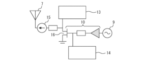
図8は、実施の形態3に係るマイクロ波反応炉の発振器の回路図である。発振器8は、発振源9と、少なくとも1段のトランジスタを含む増幅器10と、増幅器10の最終段トランジスタ11とアンテナ7との間に接続された反射波モニタ回路12とを有する。発振源9は、マイクロ波の電気信号を発生させる。増幅器10は、発振源9からのマイクロ波の電気信号を増幅する。増幅器10の最終段トランジスタ11はGaNトランジスタである。GaNトランジスタが増幅した電気信号はアンテナ7に供給される。アンテナ7はマイクロ波を放射する。
図8は、実施の形態3に係るマイクロ波反応炉の発振器の回路図である。発振器8は、発振源9と、少なくとも1段のトランジスタを含む増幅器10と、増幅器10の最終段トランジスタ11とアンテナ7との間に接続された反射波モニタ回路12とを有する。発振源9は、マイクロ波の電気信号を発生させる。増幅器10は、発振源9からのマイクロ波の電気信号を増幅する。増幅器10の最終段トランジスタ11はGaNトランジスタである。GaNトランジスタが増幅した電気信号はアンテナ7に供給される。アンテナ7はマイクロ波を放射する。
ドレイン電圧制御回路13は最終段トランジスタ11のドレイン電圧を制御する。ゲート電圧制御回路14は最終段トランジスタ11のゲート電圧を制御する。反射波モニタ回路12は、アンテナ7から戻ってくる反射波の強度をモニタする。反射波モニタ回路12は、例えば、方向性結合器に検波ダイオードを接続する等の回路により構成される。
反射波の強度が閾値を超えると、反射波モニタ回路12は、最終段トランジスタ11のドレイン電圧を速やかに0V又は低電圧に下げるようにドレイン電圧制御回路13を制御するか、又は、最終段トランジスタ11の動作電流を下げるようにゲート電圧制御回路14を制御する。このような制御を行う反射波の強度の閾値は、例えば、発振器8の出力信号の1/2倍から数倍の強度である。
続いて、本実施の形態の効果を比較例と比較して説明する。図9は、比較例に係る発振器の回路図である。比較例では、アイソレータ15が、増幅器10の最終段トランジスタであるLDMOSトランジスタ16とアンテナ7の間に接続されている。
実施の形態1と同様に反応炉1の開口3の面積を反応炉1の内壁のうち反応物質2に覆われていない部分の面積の1/10以下にしているため、反応炉1からの反射波は抑制されている。しかし、反応物質2を充填していない等の予期せぬ突発的な事象によりアンテナ7に大きな反射波が入る場合がある。このような過大な信号により発振器8の最終段トランジスタ11等が破損する場合がある。これを防ぐために、比較例ではアイソレータ15を設けている。しかし、アイソレータ15は磁気回路であって、出力が300Wと大きくなると大型化すると共に高コストとなる。また、アイソレータ15には反射波を熱に変える抵抗が内蔵されている。しかし、大電力に対応するためには抵抗も大型化される。さらに、反射電力が大きい場合に抵抗が焼損してしまう場合もある。従って、復旧にはアイソレータ15の交換を要して時間とコストが多大になる。
これに対して、本実施の形態では、増幅器10の最終段トランジスタ11とアンテナ7との間に反射波モニタ回路12を設けている。大きな反射波がくると、反射波モニタ回路12は、最終段トランジスタ11のドレイン電圧又は動作電流を下げるように制御する。これにより、大きな反射波が発生しても、アンテナ7に接続された増幅器10が破壊されるのを防ぐことができる。また、最終段トランジスタ11のドレイン電圧又は動作電流を変えるだけなので、復旧する場合にも単に両電圧を元に戻すだけでよい。従って、部品交換することなく短時間で復旧することができる。
本実施の形態ではアンテナ7毎に反射波モニタ回路12を設けている。これに限らず、複数のアンテナ7に対して1つの反射波モニタ回路12を設け、アンテナ7から反射波がくると複数の発振器8の全ての最終段トランジスタ11のドレイン電圧又は動作電流を下げるように制御してもよい。例えば10×10のアレイアンテナの場合に10個又は25個のアンテナ7のブロックの一つの発振器8に反射波モニタ回路12を設け、同一ブロックの全ての最終段トランジスタ11のドレイン電圧又は動作電流を下げるように一括で制御してもよい。複数のアンテナについて一括制御することにより制御機器の個数が減ってコストを下げることができる。
マイクロ波反応炉は自由空間でなく閉空間であり、マイクロ波ビームの方向が固定されている。このため、一般のレーダ等のアレイアンテナと異なり外部から特定の1個のみに反射が入る可能性は無く、全体的に反射波が入る。従って、このようなブロック毎の保護回路であっても有効である。
また、本実施の形態では、増幅器10の最終段トランジスタ11はGaNトランジスタである。GaNトランジスタは従来のLDMOSより効率が良いため、マイクロ波反応炉のエネルギー効率を改善できる。さらに、GaNトランジスタはLDMOSより耐圧が高く、高電圧が印加されても破損し難いため、反射波に対して大きな耐性を有する。
実施の形態4.
図10は実施の形態4に係るマイクロ波反応炉を示す断面図である。反応炉1に複数の開口3が設けられている。複数のマイクロ波発生器4がマイクロ波ビーム5を複数の開口3の中心部にそれぞれ集中させて反応炉1の内部にマイクロ波ビーム5を入射させる。なお、図面では開口3とマイクロ波発生器4が2つであるが、これに限らず3つ以上でもよい。
図10は実施の形態4に係るマイクロ波反応炉を示す断面図である。反応炉1に複数の開口3が設けられている。複数のマイクロ波発生器4がマイクロ波ビーム5を複数の開口3の中心部にそれぞれ集中させて反応炉1の内部にマイクロ波ビーム5を入射させる。なお、図面では開口3とマイクロ波発生器4が2つであるが、これに限らず3つ以上でもよい。
各開口3の寸法はマイクロ波ビーム5の半波長より長く、各開口3の面積は反応炉1の内壁のうち反応物質2に覆われていない部分の面積の1/10以下である。各開口3から入射されたマイクロ波が反応炉1の内壁で反射することなく他の開口3に直接的に入ることがないように複数の開口3が配置されている。
反応炉1が大きい場合又はマイクロ波の電力が非常に大きい場合には、上記のように複数の開口3から複数のマイクロ波を反応炉1内に供給することになる。しかし、反応炉1が大きいために炉内の多重反射による電磁界の分布が不均一になってしまう。この結果、反応物質2に照射されるマイクロ波が均質にならず、反応が一様に進まないことにより収率の減少又は反応効率の劣化が生じる。
各開口3から閉空間である反応炉1の内部に入射されたマイクロ波は多重反射して山谷を有する電磁波の定在波が生じる。マイクロ波の位相を変えることで定在波の山谷を変えることができる。また、従来のマグネトロンではマイクロ波の位相制御は困難であったが、発振器8はGaN等の半導体を用いた発振器であるため、マイクロ波の位相を精密に制御することができる。
そこで、複数のマイクロ波発生器4の発振器8は、反応炉1の内部のマイクロ波分布(電磁界分布)が均一になるように、複数の開口3から入射されるマイクロ波の位相をそれぞれ制御する。これにより、炉内の反応物質2にマイクロ波を均一に照射できるため、反応物質2の反応を均一にすることができる。予めシミュレーションして最適な位相制御を求めてもよいし、位相を変えながら収率の良い条件にセットしてもよい。
実施の形態5.
図11は、実施の形態5に係るマイクロ波反応炉を示す断面図である。反応炉1から生じるガスを封じ込めるために反応炉1を防爆壁17が囲んでいる。発振器8は防爆壁17の外側に設けられるため、発振器8は防爆仕様とする必要はなく、安価に製造できる。
図11は、実施の形態5に係るマイクロ波反応炉を示す断面図である。反応炉1から生じるガスを封じ込めるために反応炉1を防爆壁17が囲んでいる。発振器8は防爆壁17の外側に設けられるため、発振器8は防爆仕様とする必要はなく、安価に製造できる。
反応炉1内の反応物質2が飛散又はガス化してマイクロ波発生器4のアンテナ7を損傷する可能性がある。そこで、遮蔽板18を反応炉1の開口3に設ける。遮蔽板18は反応炉1の内部の物質が開口3から反応炉1の外に出るのを防ぐ。従って、反応炉1の内部で発生する物質がマイクロ波発生器4のアンテナ7に付着しないため、アンテナ7の劣化を防止することができる。マイクロ波ビーム5は遮蔽板18を透過できる。
遮蔽板18は、マイクロ波ビーム5の半波長の厚さを持つ石英板である。遮蔽板18を通るマイクロ波は遮蔽板18の上面と下面で反射するが、遮蔽板18の上面からの反射波と下面からの反射波が打ち消し合う。従って、不要な反射によるマイクロ波の給電量の減少を抑制できる。
なお、遮蔽板18は石英板に限らず、マイクロ波が透過できるガラス、樹脂等の誘電体板であればよく、繊維状材料を用いた誘電体板でもよい。また、遮蔽板18は一枚の誘電体板に限らず、複数枚の誘電体板でもよい。
実施の形態6.
図12は、実施の形態6に係るマイクロ波反応炉を示す断面図である。実施の形態5の遮蔽板18は石英板であるため、マイクロ波が通過することにより石英のtanδにより発熱する。石英のtanδ=0.00025で2.45GHzの誘電損による発熱量を計算すると100kWで78W、温度上昇は200℃程度である。従って、100kW程度までは使用可能であるが1MW以上の大電力では発熱が780W以上、温度上昇が2000℃以上となり損傷する可能性がある。この発熱は石英板の誘電損が原因であるため石英板の板厚を半波長より十分薄くすれば誘電体損を下げることができる。しかし、反応炉内外の圧力差により石英薄膜が破損する危険性がある。
図12は、実施の形態6に係るマイクロ波反応炉を示す断面図である。実施の形態5の遮蔽板18は石英板であるため、マイクロ波が通過することにより石英のtanδにより発熱する。石英のtanδ=0.00025で2.45GHzの誘電損による発熱量を計算すると100kWで78W、温度上昇は200℃程度である。従って、100kW程度までは使用可能であるが1MW以上の大電力では発熱が780W以上、温度上昇が2000℃以上となり損傷する可能性がある。この発熱は石英板の誘電損が原因であるため石英板の板厚を半波長より十分薄くすれば誘電体損を下げることができる。しかし、反応炉内外の圧力差により石英薄膜が破損する危険性がある。
そこで、本実施の形態では、遮蔽板18は、2枚の誘電体薄膜19,20と、2枚の誘電体薄膜19,20の間に挟まれマイクロ波ビーム5の1/4波長の厚さを持つハニカム材21とを有する。誘電体薄膜19,20は、板厚が半波長より十分薄い石英薄膜である。従って、不要な発熱を抑制することができる。
ハニカム材21は、マイクロ波への影響が少ない比誘電率が1に近い誘電体であり、例えばガラス繊維強化プラスチック等である。2枚の誘電体薄膜19,20を1/4波長離して設けることで反射波を相殺することができる。従って、不要な反射によるマイクロ波の給電量の減少を抑制できる。また、2枚の誘電体薄膜19,20の間にハニカム材21を挟むことにより、反応炉1から受ける圧力に対して石英薄膜を強度的に支えることができる。
なお、誘電体薄膜19,20は石英薄膜に限らず、マイクロ波が透過できるガラス、樹脂等の誘電体薄膜であればよく、繊維状材料を用いた誘電体薄膜でもよい。また、誘電体薄膜19,20は2枚の薄膜でなくても複数枚の薄膜でもよい。
1 反応炉、2 反応物質、3 開口、4 マイクロ波発生器、5 マイクロ波ビーム、6 チャンバ、7 アンテナ、8 発振器、10 増幅器、11 最終段トランジスタ、12 反射波モニタ回路、18 遮蔽板、19,20 誘電体薄膜、21 ハニカム材
Claims (11)
- 反応物質を収納する反応炉と、
マイクロ波ビームを発生させるマイクロ波発生器とを備え、
前記反応炉に開口が設けられ、
前記マイクロ波発生器は、前記マイクロ波ビームを前記開口の中心部に集中させて前記反応炉の内部に前記マイクロ波ビームを入射させ、
前記反応炉の内壁は前記マイクロ波ビームを反射し、
前記開口の寸法は、前記マイクロ波ビームの半波長より長く、
前記開口の面積は、前記反応炉の内壁のうち前記反応物質に覆われていない部分の面積の1/10以下であることを特徴とするマイクロ波反応炉。 - 前記マイクロ波発生器は、導波路を用いずに前記反応炉の内部に前記マイクロ波ビームを直接的に入射させることを特徴とする請求項1に記載のマイクロ波反応炉。
- 前記マイクロ波発生器は、
前記開口に接続され、導体により構成され、前記マイクロ波ビームを形成するための空間を囲むチャンバと、
前記チャンバの壁面に設けられ、前記チャンバの内部で前記マイクロ波ビームを空間合成する複数のアンテナと、
位相制御したマイクロ波の電気信号を前記複数のアンテナにそれぞれ供給する複数の発振器とを有することを特徴とする請求項1又は2に記載のマイクロ波反応炉。 - 前記複数のアンテナは円形アレイアンテナであることを特徴とする請求項3に記載のマイクロ波反応炉。
- 前記発振器は、少なくとも1段のトランジスタを含み前記マイクロ波の電気信号を増幅させる増幅器と、前記増幅器の最終段トランジスタと前記アンテナとの間に接続された反射波モニタ回路とを有し、
前記反射波モニタ回路は、前記アンテナから戻ってくる反射波の強度をモニタし、前記反射波の強度が閾値を超えると前記最終段トランジスタのドレイン電圧又は動作電流を下げるように制御することを特徴とする請求項3又は4に記載のマイクロ波反応炉。 - 前記反射波モニタ回路は、前記反射波の強度が閾値を超えると前記複数の発振器の全ての前記最終段トランジスタのドレイン電圧又は動作電流を下げるように制御することを特徴とする請求項5に記載のマイクロ波反応炉。
- 前記最終段トランジスタはGaNトランジスタであることを特徴とする請求項5又は6に記載のマイクロ波反応炉。
- 前記反応炉に複数の前記開口が設けられ、
各開口から入射された前記マイクロ波ビームが前記反応炉の内壁で反射することなく他の開口に直接的に入ることがないように複数の前記開口は配置され、
前記複数の発振器は、前記反応炉の内部のマイクロ波分布が均一になるように、複数の前記開口から入射される前記マイクロ波ビームの位相をそれぞれ制御することを特徴とする請求項3~7の何れか1項に記載のマイクロ波反応炉。 - 前記反応炉の前記開口に設けられ、前記反応炉の内部の物質が前記開口から前記反応炉の外に出るのを防ぐ遮蔽板を更に備えることを特徴とする請求項1~8の何れか1項に記載のマイクロ波反応炉。
- 前記遮蔽板は、前記マイクロ波ビームの半波長の厚さを持つ誘電体板であることを特徴とする請求項9に記載のマイクロ波反応炉。
- 前記遮蔽板は、2枚の誘電体薄膜と、前記2枚の誘電体薄膜の間に挟まれ前記マイクロ波ビームの1/4波長の厚さを持つハニカム材とを有することを特徴とする請求項9に記載のマイクロ波反応炉。
Priority Applications (3)
| Application Number | Priority Date | Filing Date | Title |
|---|---|---|---|
| PCT/JP2023/030188 WO2025041274A1 (ja) | 2023-08-22 | 2023-08-22 | マイクロ波反応炉 |
| JP2025541225A JPWO2025041274A1 (ja) | 2023-08-22 | 2023-08-22 | |
| CN202380100440.1A CN121712584A (zh) | 2023-08-22 | 2023-08-22 | 微波反应炉 |
Applications Claiming Priority (1)
| Application Number | Priority Date | Filing Date | Title |
|---|---|---|---|
| PCT/JP2023/030188 WO2025041274A1 (ja) | 2023-08-22 | 2023-08-22 | マイクロ波反応炉 |
Publications (1)
| Publication Number | Publication Date |
|---|---|
| WO2025041274A1 true WO2025041274A1 (ja) | 2025-02-27 |
Family
ID=94731990
Family Applications (1)
| Application Number | Title | Priority Date | Filing Date |
|---|---|---|---|
| PCT/JP2023/030188 Pending WO2025041274A1 (ja) | 2023-08-22 | 2023-08-22 | マイクロ波反応炉 |
Country Status (3)
| Country | Link |
|---|---|
| JP (1) | JPWO2025041274A1 (ja) |
| CN (1) | CN121712584A (ja) |
| WO (1) | WO2025041274A1 (ja) |
Citations (6)
| Publication number | Priority date | Publication date | Assignee | Title |
|---|---|---|---|---|
| JP2008302281A (ja) * | 2007-06-06 | 2008-12-18 | Shikoku Instrumentation Co Ltd | マイクロ波化学反応装置および方法 |
| JP2016064318A (ja) * | 2014-02-27 | 2016-04-28 | マイクロ波化学株式会社 | 化学反応装置 |
| JP2018196876A (ja) * | 2017-05-23 | 2018-12-13 | マイクロ波化学株式会社 | 処理装置 |
| JP2019181449A (ja) * | 2018-07-26 | 2019-10-24 | マイクロ波化学株式会社 | カラム |
| JP2021125468A (ja) * | 2020-02-07 | 2021-08-30 | マイクロ波化学株式会社 | マイクロ波処理装置、マイクロ波導入装置、及びマイクロ波処理方法 |
| JP2022059529A (ja) * | 2020-10-01 | 2022-04-13 | マイクロ波化学株式会社 | マイクロ波処理装置、及びマイクロ波処理方法 |
-
2023
- 2023-08-22 CN CN202380100440.1A patent/CN121712584A/zh active Pending
- 2023-08-22 WO PCT/JP2023/030188 patent/WO2025041274A1/ja active Pending
- 2023-08-22 JP JP2025541225A patent/JPWO2025041274A1/ja active Pending
Patent Citations (7)
| Publication number | Priority date | Publication date | Assignee | Title |
|---|---|---|---|---|
| JP2008302281A (ja) * | 2007-06-06 | 2008-12-18 | Shikoku Instrumentation Co Ltd | マイクロ波化学反応装置および方法 |
| JP2016064318A (ja) * | 2014-02-27 | 2016-04-28 | マイクロ波化学株式会社 | 化学反応装置 |
| JP2018196876A (ja) * | 2017-05-23 | 2018-12-13 | マイクロ波化学株式会社 | 処理装置 |
| JP2018196879A (ja) * | 2017-05-23 | 2018-12-13 | マイクロ波化学株式会社 | 処理装置 |
| JP2019181449A (ja) * | 2018-07-26 | 2019-10-24 | マイクロ波化学株式会社 | カラム |
| JP2021125468A (ja) * | 2020-02-07 | 2021-08-30 | マイクロ波化学株式会社 | マイクロ波処理装置、マイクロ波導入装置、及びマイクロ波処理方法 |
| JP2022059529A (ja) * | 2020-10-01 | 2022-04-13 | マイクロ波化学株式会社 | マイクロ波処理装置、及びマイクロ波処理方法 |
Also Published As
| Publication number | Publication date |
|---|---|
| JPWO2025041274A1 (ja) | 2025-02-27 |
| CN121712584A (zh) | 2026-03-20 |
Similar Documents
| Publication | Publication Date | Title |
|---|---|---|
| Rostov et al. | Two-wave Ka-band nanosecond relativistic Cherenkov oscillator | |
| JP5208547B2 (ja) | 電力合成器およびマイクロ波導入機構 | |
| ES2273850T3 (es) | Adaptador de guia de ondas de transicion de modos para una red de rejilla cuasioptica. | |
| JP4183934B2 (ja) | マイクロ波プラズマ処理装置、マイクロ波プラズマ処理方法及びマイクロ波給電装置 | |
| Gardelle et al. | A compact THz source: 100/200 GHz operation of a cylindrical Smith–Purcell free-electron laser | |
| Wang et al. | Research on an overmoded $ Ka $-band RBWO operating in TM 02 mode with low-guiding magnetic field | |
| Kazantsev et al. | Laser Controlled Loop Antenna | |
| Guan et al. | A 0.4-THz second harmonic gyrotron with quasi-optical confocal cavity | |
| Wagner et al. | Extension of the multi-frequency ECRH system at ASDEX upgrade | |
| Zhang et al. | Suppression of the Higher-Order Azimuthal Mode Competition in an ${X} $-Band Triaxial Klystron Amplifier With a Slotted Coaxial Waveguide | |
| JP3751967B1 (ja) | マグネトロン発振装置 | |
| WO2025041274A1 (ja) | マイクロ波反応炉 | |
| Horikoshi et al. | Engineering of microwave heating | |
| Gallerano et al. | High power THz sources and applications at ENEA-Frascati | |
| Lukin et al. | THz Oscillators Based on Cherenkov, Smith—Purcell and Hybrid Radiation Effects | |
| Totmeninov et al. | Repetitive ${{X}} $-Band Relativistic Traveling Wave Oscillator | |
| US20150207226A1 (en) | Broadband Electromagnetic Radiators and Antennas | |
| Wu et al. | A Gaussian-like beam output system for high-power Ka-band gyro-TWT | |
| KR20240029457A (ko) | 소형 경량화된 고주파 플라즈마 응용장치 | |
| WO2019009174A1 (ja) | マイクロ波処理装置 | |
| JP3856153B1 (ja) | マグネトロン発振装置 | |
| Yao et al. | Initial investigation on diffractive-wave feedback mechanism of confocal gyro-TWAs | |
| Kumar et al. | Generation of microwave free-electron laser radiation using sheet electron beam and planar electromagnetic wiggler | |
| Brand | Development and applications of frequency tunable, submillimeter wave gyrotrons | |
| Gormezano | RF Systems for Heating and |
Legal Events
| Date | Code | Title | Description |
|---|---|---|---|
| 121 | Ep: the epo has been informed by wipo that ep was designated in this application |
Ref document number: 23949735 Country of ref document: EP Kind code of ref document: A1 |
|
| ENP | Entry into the national phase |
Ref document number: 2025541225 Country of ref document: JP Kind code of ref document: A |
|
| WWE | Wipo information: entry into national phase |
Ref document number: 2025541225 Country of ref document: JP |
|
| NENP | Non-entry into the national phase |
Ref country code: DE |