WO2025041274A1 - Réacteur à micro-ondes - Google Patents
Réacteur à micro-ondes Download PDFInfo
- Publication number
- WO2025041274A1 WO2025041274A1 PCT/JP2023/030188 JP2023030188W WO2025041274A1 WO 2025041274 A1 WO2025041274 A1 WO 2025041274A1 JP 2023030188 W JP2023030188 W JP 2023030188W WO 2025041274 A1 WO2025041274 A1 WO 2025041274A1
- Authority
- WO
- WIPO (PCT)
- Prior art keywords
- microwave
- reactor
- opening
- microwaves
- reflected wave
- Prior art date
- Legal status (The legal status is an assumption and is not a legal conclusion. Google has not performed a legal analysis and makes no representation as to the accuracy of the status listed.)
- Pending
Links
Images


Classifications
-
- B—PERFORMING OPERATIONS; TRANSPORTING
- B01—PHYSICAL OR CHEMICAL PROCESSES OR APPARATUS IN GENERAL
- B01J—CHEMICAL OR PHYSICAL PROCESSES, e.g. CATALYSIS OR COLLOID CHEMISTRY; THEIR RELEVANT APPARATUS
- B01J19/00—Chemical, physical or physico-chemical processes in general; Their relevant apparatus
- B01J19/08—Processes employing the direct application of electric or wave energy, or particle radiation; Apparatus therefor
- B01J19/12—Processes employing the direct application of electric or wave energy, or particle radiation; Apparatus therefor employing electromagnetic waves
Definitions
- This disclosure relates to microwave reactors.
- microwaves are supplied to the inside of the reactor through a waveguide. Because the opening area of the waveguide is small, few microwaves are reflected back to the waveguide. The current flowing through the conductor in the tube wall heats the waveguide, and losses also occur in the waveguide. However, if the reactor is not large-scale, microwaves of a few kW level are sufficient, so the heat and loss generated in the waveguide are at an acceptable level. On the other hand, in large-scale plants, microwaves of high power, such as hundreds of kW to tens of MW, must be supplied, so the heat and loss generated in the waveguide cannot be ignored.
- the waveguide WRI-26 is a narrow tube with a cross-section of 8.4 cm x 4.2 cm. As a result, the wall currents generated when 1 MW microwaves propagate through the tube are concentrated in an extremely small area of no more than 8 cm, resulting in a large amount of heat and loss.
- microwaves were generated by an oscillator using a magnetron.
- magnetrons have poor frequency purity and phase stability, making it difficult to synthesize microwaves from multiple magnetrons.
- the microwaves that can be generated by a single magnetron are limited to 10 kW or less at 2.45 GHz, for example, making it difficult to generate high-power microwaves exceeding 10 kW.
- the efficiency drops to 60% or less at high powers such as 10 kW, making it impossible to generate high-power, highly efficient microwaves.
- a device has been proposed in which an antenna is installed inside a reactor without using a waveguide (see, for example, Patent Document 1).
- microwaves reflected by the inner wall of the reactor may return directly to the antenna, destroying equipment such as the amplifier that supplies the microwaves to the antenna. For this reason, an isolator is provided between the amplifier output and the antenna to prevent reflected waves.
- the isolator becomes large and difficult to place, and isolators are expensive. For example, when irradiating high-power microwaves of more than 10 kW at 2.45 GHz, the reflected waves can destroy equipment, which can be a problem.
- This disclosure has been made to solve the problems described above, and its purpose is to obtain a microwave reactor that can suppress damage to equipment caused by reflected waves even when high-power microwaves are irradiated.
- the microwave reactor comprises a reactor for storing reactants and a microwave generator for generating a microwave beam, the reactor being provided with an opening, the microwave generator concentrating the microwave beam at the center of the opening and directing the microwave beam into the interior of the reactor, the inner wall of the reactor reflecting the microwave beam, the dimension of the opening being longer than half the wavelength of the microwave beam, and the area of the opening being 1/10 or less of the area of the portion of the inner wall of the reactor that is not covered by the reactants.
- the area of the reactor opening is set to 1/10 or less of the area of the portion of the reactor's inner wall that is not covered by the reactant. This makes it possible to prevent damage to equipment caused by reflected waves even when high-power microwaves are irradiated.
- FIG. 1 is a cross-sectional view showing a microwave reactor according to a first embodiment.
- FIG. 11 is a cross-sectional view showing a microwave reactor according to a second embodiment.
- FIG. 13 is a diagram showing the calculation results of spatially combining microwaves from a rectangular array antenna.
- FIG. 13 is a diagram showing the calculation results of spatially combining microwaves from a rectangular array antenna.
- FIG. 1 illustrates a circular array antenna.
- FIG. 13 is a diagram showing the calculation results of spatially combining microwaves from a circular array antenna.
- FIG. 13 is a diagram showing the calculation results of spatially combining microwaves from a circular array antenna.
- FIG. 11 is a circuit diagram of an oscillator of a microwave reactor according to a third embodiment.
- FIG. 11 is a circuit diagram of an oscillator according to a comparative example.
- FIG. 11 is a cross-sectional view showing a microwave reactor according to a fourth embodiment.
- FIG. 13 is a cross-sectional view showing a microwave reactor according to a fifth embodiment.
- FIG. 13 is a cross-sectional view showing a microwave reactor according to a sixth embodiment.
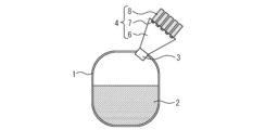
- Embodiment 1. 1 is a cross-sectional view showing a microwave reactor according to the first embodiment.
- the reactor 1 contains a reactant 2.
- the inner wall of the lower part of the reactor 1 is covered with the reactant 2.
- An opening 3 is provided in the upper part of the reactor 1 that is not covered with the reactant 2.
- a microwave generator 4 generates a microwave beam 5 that is an electromagnetic microwave wave.
- the microwave has a frequency of 0.9 GHz to 30 GHz and a wavelength of 33 cm to 1 cm.
- the microwave generator 4 is, for example, a horn antenna, and emits a microwave beam 5 into the inside of the reactor 1 through the opening 3.
- the microwaves that enter the inside of the reactor 1 are absorbed by the reactant 2, and the microwaves cause reactions such as chemical reactions, sintering, and drying of the reactant 2.
- microwaves are injected into a reactor through a waveguide, and because higher modes increase loss, the diameter of the waveguide is set to half the wavelength or less.
- the microwave generator 4 directly injects the microwave beam 5 into the inside of the reactor 1 without using a waveguide, so the dimensions of the opening 3 can be made larger than half the wavelength of the microwave beam 5.
- the microwave generator 4 focuses the microwave beam 5 on the center of the opening 3 and causes the microwave beam to enter the inside of the reactor 1. As a result, almost no microwaves are irradiated onto the end of the opening 3, so no current flows at the edge of the opening 3, suppressing the heat generation and microwave loss in the power supply area that were problems when using a waveguide.
- the reactor 1 is made of a metal such as stainless steel, the upper inner wall of the reactor 1 that is not covered by the reactant 2 reflects the microwave beam 5. Inside the reactor 1, the microwave beam 5 is multiple-reflected, and is repeatedly absorbed and reflected by the reactant 2. As a result, the reactant 2 inside the reactor 1 can be irradiated with the microwave beam 5 relatively uniformly.
- the microwave beam 5 is almost totally reflected by the inner wall of the reactor 1, and the inside of the reactor 1 has an electromagnetic field distribution resonating due to multiple reflections. If a small opening 3 is opened in the reactor 1 in this state, it becomes a state similar to so-called blackbody radiation. Of such microwaves, the reflected waves that go out from the opening 3 are a weak amount proportional to the ratio of the area of the upper inner wall of the reactor 1 that is not covered by the reactant 2 to the surface area of the opening 3. If there are many reflected waves, the amount of microwaves that reach the reactant 2 decreases, and the efficiency of the furnace decreases. In addition, there is a risk that the reflected waves will destroy the microwave generator 4.
- the amount of reflected waves needs to be suppressed to a very small amount, less than one-tenth of the microwaves inside the reactor 1.
- Embodiment 2. 2 is a cross-sectional view showing a microwave reactor according to embodiment 2.
- the microwave generator 4 has a chamber 6, a plurality of antennas 7, and a plurality of oscillators 8.
- the chamber 6 is connected to the opening 3 of the reactor 1, and surrounds a space for forming the microwave beam 5.
- the chamber 6 is made of a conductor such as a metal so as to prevent microwaves due to unnecessary side lobes generated by the microwave beam from leaking to the outside.
- the multiple antennas 7 are provided on the walls of the chamber 6, and spatially combine the microwave beams 5 inside the chamber 6.
- the multiple oscillators 8 supply phase-controlled microwave electrical signals to the multiple antennas 7, respectively.
- Each oscillator 8 has an oscillation source and a semiconductor amplifier such as GaN.
- Magnetrons generally have unstable phases and a wide frequency bandwidth. For this reason, when microwaves supplied from two or more magnetrons are combined, the combined power and efficiency drop significantly due to combination losses.
- the spacing between the antennas 7 is approximately half the wavelength, so at 2.45 GHz it is approximately 6 cm. Therefore, the size of the array antenna is approximately 60 cm x 60 cm, which is a size that is easily feasible.
- the microwave power can be increased by spatially combining the number of array antennas, so even microwaves of 30 kW or more can be easily realized. For example, if an output of 1 MW is required at 2.45 GHz, 3,333 300 W oscillators can be spatially combined. If the antennas 7 are arranged in a square, there will be approximately 58 x 58, and if they are spaced ⁇ /2 apart, each side will be approximately 3.4 m, which is easily feasible in a large furnace.
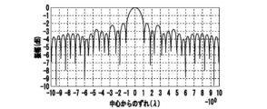
- Figure 5 shows a circular array antenna. Multiple antennas 7 are arranged in a circular area at intervals of approximately half a wavelength. The number of antennas is 363, which is almost the same as the number of antennas in the rectangular array described above. The circular array can concentrate microwaves more in the center of the aperture 3 than the rectangular array.
- Figures 6 and 7 show the calculation results of spatially combining microwaves from a circular array antenna.
- the diameter of the circular array is about 64 cm, which is equivalent to that of a square array.
- Figure 6 shows the microwave amplitude in dB on a plane 4.5 ⁇ away from the antenna.
- Figure 7 shows the cumulative power ratio accumulated according to the distance d from the center in units of 10%.
- the amplitude of the side lobe of the circular array is reduced compared to the square array in Figure 3.
- the proportion of microwaves passing through the aperture 3 with a radius of 10 ⁇ has increased to 86%. This shows that the circular array is superior to the square array in radiating more power to the aperture 3. Note that this calculation does not include the component reflected by the side wall of the chamber 6 and reaching the aperture 3, so in reality it is possible to pass an even greater proportion of the microwaves through the aperture 3.
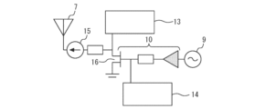
- Embodiment 3. 8 is a circuit diagram of an oscillator of a microwave reactor according to the third embodiment.
- the oscillator 8 has an oscillation source 9, an amplifier 10 including at least one stage of a transistor, and a reflected wave monitor circuit 12 connected between a final stage transistor 11 of the amplifier 10 and an antenna 7.
- the oscillation source 9 generates a microwave electric signal.
- the amplifier 10 amplifies the microwave electric signal from the oscillation source 9.
- the final stage transistor 11 of the amplifier 10 is a GaN transistor.
- the electric signal amplified by the GaN transistor is supplied to the antenna 7.
- the antenna 7 radiates microwaves.
- the drain voltage control circuit 13 controls the drain voltage of the final stage transistor 11.
- the gate voltage control circuit 14 controls the gate voltage of the final stage transistor 11.
- the reflected wave monitor circuit 12 monitors the intensity of the reflected wave returning from the antenna 7.
- the reflected wave monitor circuit 12 is configured, for example, by a circuit such as a directional coupler connected to a detection diode.
- the reflected wave monitor circuit 12 controls the drain voltage control circuit 13 to quickly lower the drain voltage of the final stage transistor 11 to 0 V or a low voltage, or controls the gate voltage control circuit 14 to lower the operating current of the final stage transistor 11.
- the threshold of the strength of the reflected wave for performing such control is, for example, 1/2 to several times the strength of the output signal of the oscillator 8.
- FIG. 9 is a circuit diagram of an oscillator according to the comparative example.
- an isolator 15 is connected between an LDMOS transistor 16, which is the final stage transistor of the amplifier 10, and an antenna 7.
- the area of the opening 3 of the reactor 1 is set to 1/10 or less of the area of the part of the inner wall of the reactor 1 that is not covered by the reactant 2, so that the reflected wave from the reactor 1 is suppressed.
- a large reflected wave may enter the antenna 7 due to an unexpected sudden event such as not filling the reactant 2.
- Such an excessive signal may damage the final stage transistor 11 of the oscillator 8.
- an isolator 15 is provided in the comparative example.
- the isolator 15 is a magnetic circuit, and if the output is increased to 300 W, it becomes large and expensive.
- the isolator 15 has a built-in resistor that converts the reflected wave into heat.
- the resistor is also large in size to handle large power.
- the reflected power is large, the resistor may burn out. Therefore, the isolator 15 must be replaced to restore operation, which takes a lot of time and costs.
- a reflected wave monitor circuit 12 is provided between the final stage transistor 11 of the amplifier 10 and the antenna 7.
- the reflected wave monitor circuit 12 controls the drain voltage or operating current of the final stage transistor 11 to be lowered. This makes it possible to prevent the amplifier 10 connected to the antenna 7 from being destroyed even if a large reflected wave occurs. Also, because only the drain voltage or operating current of the final stage transistor 11 is changed, recovery can be achieved by simply restoring both voltages to their original state. Therefore, recovery can be achieved in a short time without the need to replace parts.
- a reflected wave monitor circuit 12 is provided for each antenna 7.
- one reflected wave monitor circuit 12 may be provided for multiple antennas 7, and when a reflected wave arrives from an antenna 7, the drain voltage or operating current of all the final stage transistors 11 of multiple oscillators 8 may be controlled to be lowered.
- a reflected wave monitor circuit 12 may be provided for one oscillator 8 in a block of 10 or 25 antennas 7, and all the final stage transistors 11 in the same block may be controlled collectively to be lowered in drain voltage or operating current. By controlling multiple antennas collectively, the number of control devices can be reduced, thereby reducing costs.
- a microwave reactor is not a free space but a closed space, and the direction of the microwave beam is fixed. For this reason, unlike array antennas such as those used in general radars, there is no possibility of a reflection from the outside hitting just one specific unit, and the reflected wave hits the entire reactor. Therefore, even a protection circuit for each block like this is effective.
- the final stage transistor 11 of the amplifier 10 is a GaN transistor.
- GaN transistors are more efficient than conventional LDMOS transistors, and therefore can improve the energy efficiency of the microwave reactor. Furthermore, GaN transistors have a higher voltage resistance than LDMOS transistors and are less likely to be damaged even when high voltages are applied, and therefore have a high resistance to reflected waves.
- Embodiment 4. 10 is a cross-sectional view showing a microwave reactor according to embodiment 4.
- a plurality of openings 3 are provided in the reactor 1.
- a plurality of microwave generators 4 focus microwave beams 5 on the centers of the plurality of openings 3, respectively, and cause the microwave beams 5 to enter the inside of the reactor 1. Note that, although the figure shows two openings 3 and two microwave generators 4, the number is not limited thereto, and three or more may be used.
- each opening 3 are longer than half the wavelength of the microwave beam 5, and the area of each opening 3 is 1/10 or less of the area of the portion of the inner wall of the reactor 1 that is not covered by the reactant 2.
- Multiple openings 3 are arranged so that the microwaves incident from each opening 3 do not enter directly into other openings 3 without being reflected by the inner wall of the reactor 1.
- the reactor 1 When the reactor 1 is large or the microwave power is very high, multiple microwaves are supplied into the reactor 1 from multiple openings 3 as described above. However, because the reactor 1 is large, the electromagnetic field distribution becomes uneven due to multiple reflections inside the reactor. As a result, the microwaves irradiated to the reactant 2 are not homogeneous, and the reaction does not proceed uniformly, resulting in a decrease in yield or deterioration of reaction efficiency.
- Microwaves entering the closed space inside the reactor 1 from each opening 3 are reflected multiple times, generating standing electromagnetic waves with peaks and valleys.
- the peaks and valleys of the standing waves can be changed by changing the phase of the microwaves.
- the oscillator 8 is an oscillator that uses semiconductors such as GaN, it is possible to precisely control the phase of the microwaves.
- the oscillators 8 of the multiple microwave generators 4 each control the phase of the microwaves incident from the multiple openings 3 so that the microwave distribution (electromagnetic field distribution) inside the reactor 1 is uniform. This allows the microwaves to be uniformly irradiated onto the reactants 2 inside the reactor, making the reaction of the reactants 2 uniform.
- the optimal phase control can be determined by performing a simulation in advance, or the phase can be changed to set conditions that provide good yields.
- Embodiment 5. 11 is a cross-sectional view showing a microwave reactor according to embodiment 5.
- the reactor 1 is surrounded by an explosion-proof wall 17 to contain gas generated from the reactor 1. Since the oscillator 8 is provided outside the explosion-proof wall 17, the oscillator 8 does not need to be explosion-proof and can be manufactured at low cost.
- a shielding plate 18 is provided at the opening 3 of the reactor 1.
- the shielding plate 18 prevents the material inside the reactor 1 from escaping from the opening 3 to the outside of the reactor 1. Therefore, the material generated inside the reactor 1 does not adhere to the antenna 7 of the microwave generator 4, preventing deterioration of the antenna 7.
- the microwave beam 5 can pass through the shielding plate 18.
- the shielding plate 18 is a quartz plate with a thickness of half the wavelength of the microwave beam 5.
- the microwaves passing through the shielding plate 18 are reflected by the upper and lower surfaces of the shielding plate 18, but the reflected waves from the upper and lower surfaces of the shielding plate 18 cancel each other out. This makes it possible to suppress a decrease in the amount of microwave power supply due to unnecessary reflections.
- the shielding plate 18 is not limited to a quartz plate, but may be any dielectric plate such as glass or resin that allows microwaves to pass through, or may be a dielectric plate made of a fibrous material. Also, the shielding plate 18 is not limited to a single dielectric plate, but may be multiple dielectric plates.
- the dielectric loss of the quartz plate Since this heat generation is caused by the dielectric loss of the quartz plate, the dielectric loss can be reduced by making the plate thickness of the quartz plate sufficiently thinner than the half wavelength. However, there is a risk that the quartz thin film may be damaged due to the pressure difference between the inside and outside of the reactor.
- the shielding plate 18 has two dielectric thin films 19, 20 and a honeycomb material 21 sandwiched between the two dielectric thin films 19, 20 and having a thickness of 1/4 wavelength of the microwave beam 5.
- the dielectric thin films 19, 20 are quartz thin films with a plate thickness that is sufficiently thinner than half the wavelength. Therefore, unnecessary heat generation can be suppressed.
- the honeycomb material 21 is a dielectric with a relative dielectric constant close to 1 that has little effect on microwaves, such as glass fiber reinforced plastic.
- the honeycomb material 21 By arranging the two dielectric thin films 19, 20 1/4 wavelength apart, the reflected waves can be cancelled out. This makes it possible to suppress a decrease in the amount of microwave power supply due to unnecessary reflections.
- the quartz thin film can be strengthened to support the pressure received from the reactor 1.
- the dielectric thin films 19 and 20 are not limited to quartz thin films, but may be made of glass, resin, or other dielectric thin films that are permeable to microwaves, and may also be made of a fibrous material. Also, the dielectric thin films 19 and 20 do not have to consist of two thin films, but may consist of multiple thin films.
Landscapes
- Chemical & Material Sciences (AREA)
- Physics & Mathematics (AREA)
- Electromagnetism (AREA)
- Health & Medical Sciences (AREA)
- General Health & Medical Sciences (AREA)
- Toxicology (AREA)
- Organic Chemistry (AREA)
- Chemical Kinetics & Catalysis (AREA)
- Constitution Of High-Frequency Heating (AREA)
Abstract
La présente invention concerne un réacteur (1) qui reçoit un réactif (2). L'invention concerne également un générateur de micro-ondes (4) qui génère un faisceau de micro-ondes (5). Une ouverture (3) est aménagée sur le réacteur (1). Le générateur de micro-ondes (4) concentre le faisceau de micro-ondes (5) sur la partie centrale de l'ouverture (3), et amène le faisceau de micro-ondes (5) à entrer à l'intérieur du réacteur (1). La paroi interne du réacteur (1) réfléchit le faisceau de micro-ondes (5). La taille de l'ouverture (3) est plus longue que la demi-longueur d'onde du faisceau de micro-ondes (5). La surface de l'ouverture (3) est égale ou inférieure à 1/10 de la surface d'une portion, de la paroi interne du réacteur (1), non recouverte par le réactif (2).
Priority Applications (3)
| Application Number | Priority Date | Filing Date | Title |
|---|---|---|---|
| PCT/JP2023/030188 WO2025041274A1 (fr) | 2023-08-22 | 2023-08-22 | Réacteur à micro-ondes |
| JP2025541225A JPWO2025041274A1 (fr) | 2023-08-22 | 2023-08-22 | |
| CN202380100440.1A CN121712584A (zh) | 2023-08-22 | 2023-08-22 | 微波反应炉 |
Applications Claiming Priority (1)
| Application Number | Priority Date | Filing Date | Title |
|---|---|---|---|
| PCT/JP2023/030188 WO2025041274A1 (fr) | 2023-08-22 | 2023-08-22 | Réacteur à micro-ondes |
Publications (1)
| Publication Number | Publication Date |
|---|---|
| WO2025041274A1 true WO2025041274A1 (fr) | 2025-02-27 |
Family
ID=94731990
Family Applications (1)
| Application Number | Title | Priority Date | Filing Date |
|---|---|---|---|
| PCT/JP2023/030188 Pending WO2025041274A1 (fr) | 2023-08-22 | 2023-08-22 | Réacteur à micro-ondes |
Country Status (3)
| Country | Link |
|---|---|
| JP (1) | JPWO2025041274A1 (fr) |
| CN (1) | CN121712584A (fr) |
| WO (1) | WO2025041274A1 (fr) |
Citations (6)
| Publication number | Priority date | Publication date | Assignee | Title |
|---|---|---|---|---|
| JP2008302281A (ja) * | 2007-06-06 | 2008-12-18 | Shikoku Instrumentation Co Ltd | マイクロ波化学反応装置および方法 |
| JP2016064318A (ja) * | 2014-02-27 | 2016-04-28 | マイクロ波化学株式会社 | 化学反応装置 |
| JP2018196876A (ja) * | 2017-05-23 | 2018-12-13 | マイクロ波化学株式会社 | 処理装置 |
| JP2019181449A (ja) * | 2018-07-26 | 2019-10-24 | マイクロ波化学株式会社 | カラム |
| JP2021125468A (ja) * | 2020-02-07 | 2021-08-30 | マイクロ波化学株式会社 | マイクロ波処理装置、マイクロ波導入装置、及びマイクロ波処理方法 |
| JP2022059529A (ja) * | 2020-10-01 | 2022-04-13 | マイクロ波化学株式会社 | マイクロ波処理装置、及びマイクロ波処理方法 |
-
2023
- 2023-08-22 CN CN202380100440.1A patent/CN121712584A/zh active Pending
- 2023-08-22 WO PCT/JP2023/030188 patent/WO2025041274A1/fr active Pending
- 2023-08-22 JP JP2025541225A patent/JPWO2025041274A1/ja active Pending
Patent Citations (7)
| Publication number | Priority date | Publication date | Assignee | Title |
|---|---|---|---|---|
| JP2008302281A (ja) * | 2007-06-06 | 2008-12-18 | Shikoku Instrumentation Co Ltd | マイクロ波化学反応装置および方法 |
| JP2016064318A (ja) * | 2014-02-27 | 2016-04-28 | マイクロ波化学株式会社 | 化学反応装置 |
| JP2018196876A (ja) * | 2017-05-23 | 2018-12-13 | マイクロ波化学株式会社 | 処理装置 |
| JP2018196879A (ja) * | 2017-05-23 | 2018-12-13 | マイクロ波化学株式会社 | 処理装置 |
| JP2019181449A (ja) * | 2018-07-26 | 2019-10-24 | マイクロ波化学株式会社 | カラム |
| JP2021125468A (ja) * | 2020-02-07 | 2021-08-30 | マイクロ波化学株式会社 | マイクロ波処理装置、マイクロ波導入装置、及びマイクロ波処理方法 |
| JP2022059529A (ja) * | 2020-10-01 | 2022-04-13 | マイクロ波化学株式会社 | マイクロ波処理装置、及びマイクロ波処理方法 |
Also Published As
| Publication number | Publication date |
|---|---|
| JPWO2025041274A1 (fr) | 2025-02-27 |
| CN121712584A (zh) | 2026-03-20 |
Similar Documents
| Publication | Publication Date | Title |
|---|---|---|
| Rostov et al. | Two-wave Ka-band nanosecond relativistic Cherenkov oscillator | |
| JP5208547B2 (ja) | 電力合成器およびマイクロ波導入機構 | |
| ES2273850T3 (es) | Adaptador de guia de ondas de transicion de modos para una red de rejilla cuasioptica. | |
| JP4183934B2 (ja) | マイクロ波プラズマ処理装置、マイクロ波プラズマ処理方法及びマイクロ波給電装置 | |
| Gardelle et al. | A compact THz source: 100/200 GHz operation of a cylindrical Smith–Purcell free-electron laser | |
| Wang et al. | Research on an overmoded $ Ka $-band RBWO operating in TM 02 mode with low-guiding magnetic field | |
| Kazantsev et al. | Laser Controlled Loop Antenna | |
| Guan et al. | A 0.4-THz second harmonic gyrotron with quasi-optical confocal cavity | |
| Wagner et al. | Extension of the multi-frequency ECRH system at ASDEX upgrade | |
| Zhang et al. | Suppression of the Higher-Order Azimuthal Mode Competition in an ${X} $-Band Triaxial Klystron Amplifier With a Slotted Coaxial Waveguide | |
| JP3751967B1 (ja) | マグネトロン発振装置 | |
| WO2025041274A1 (fr) | Réacteur à micro-ondes | |
| Horikoshi et al. | Engineering of microwave heating | |
| Gallerano et al. | High power THz sources and applications at ENEA-Frascati | |
| Lukin et al. | THz Oscillators Based on Cherenkov, Smith—Purcell and Hybrid Radiation Effects | |
| Totmeninov et al. | Repetitive ${{X}} $-Band Relativistic Traveling Wave Oscillator | |
| US20150207226A1 (en) | Broadband Electromagnetic Radiators and Antennas | |
| Wu et al. | A Gaussian-like beam output system for high-power Ka-band gyro-TWT | |
| KR20240029457A (ko) | 소형 경량화된 고주파 플라즈마 응용장치 | |
| WO2019009174A1 (fr) | Dispositif de traitement à micro-ondes | |
| JP3856153B1 (ja) | マグネトロン発振装置 | |
| Yao et al. | Initial investigation on diffractive-wave feedback mechanism of confocal gyro-TWAs | |
| Kumar et al. | Generation of microwave free-electron laser radiation using sheet electron beam and planar electromagnetic wiggler | |
| Brand | Development and applications of frequency tunable, submillimeter wave gyrotrons | |
| Gormezano | RF Systems for Heating and |
Legal Events
| Date | Code | Title | Description |
|---|---|---|---|
| 121 | Ep: the epo has been informed by wipo that ep was designated in this application |
Ref document number: 23949735 Country of ref document: EP Kind code of ref document: A1 |
|
| ENP | Entry into the national phase |
Ref document number: 2025541225 Country of ref document: JP Kind code of ref document: A |
|
| WWE | Wipo information: entry into national phase |
Ref document number: 2025541225 Country of ref document: JP |
|
| NENP | Non-entry into the national phase |
Ref country code: DE |