WO2025041201A1 - Dispositif de mesure optique - Google Patents
Dispositif de mesure optique Download PDFInfo
- Publication number
- WO2025041201A1 WO2025041201A1 PCT/JP2023/029888 JP2023029888W WO2025041201A1 WO 2025041201 A1 WO2025041201 A1 WO 2025041201A1 JP 2023029888 W JP2023029888 W JP 2023029888W WO 2025041201 A1 WO2025041201 A1 WO 2025041201A1
- Authority
- WO
- WIPO (PCT)
- Prior art keywords
- light
- optical
- probe
- output
- measurement device
- Prior art date
- Legal status (The legal status is an assumption and is not a legal conclusion. Google has not performed a legal analysis and makes no representation as to the accuracy of the status listed.)
- Pending
Links
Images


Classifications
-
- G—PHYSICS
- G01—MEASURING; TESTING
- G01M—TESTING STATIC OR DYNAMIC BALANCE OF MACHINES OR STRUCTURES; TESTING OF STRUCTURES OR APPARATUS, NOT OTHERWISE PROVIDED FOR
- G01M11/00—Testing of optical apparatus; Testing structures by optical methods not otherwise provided for
Definitions
- the present invention relates to the measurement of incident light provided to the light receiving end of an optical element and emitted light emitted from the light emitting end of the optical element.
- test devices that test optical elements that input and output light are known (for example, Patent Documents 1 to 3).
- Such test devices have an optical probe that is in close proximity to the optical element, and an optical measurement unit.
- the optical measurement unit has an optical waveguide that provides light to the optical probe or receives light from the optical probe, and a measuring device that measures the light traveling through the optical waveguide.
- the optical probe and the optical measurement unit are separated, so the loss of light between them is not negligible.
- the present invention aims to reduce the loss of light between the optical probe and the optical measurement unit.
- the first optical measurement device is an optical measurement device that measures the output light emitted from the output end of an optical element, and is equipped with an output light probe that is close to the output end and receives the output light, an output light waveguide that receives the output light from the output light probe, and an output light meter that measures the output light traveling through the output light waveguide, and is configured such that the output light probe and the optical measurement unit are arranged on the same substrate, and the output light probe and the output light waveguide are directly connected.
- the output light emitted from the output end of the optical element is measured.
- An output light probe is located close to the output end and receives the output light.
- An optical measurement unit has an output light waveguide that receives the output light from the output light probe, and an output light meter that measures the output light traveling through the output light waveguide.
- the output light probe and the optical measurement unit are arranged on the same substrate. The output light probe and the output light waveguide are directly connected.
- the third optical measurement device is an optical measurement device that measures incident light given to a light receiving end of an optical element and emitted light emitted from the emission end of the optical element, and includes an incident optical probe that is close to the light receiving end and emits the incident light, an emission optical probe that is close to the emission end and receives the emission light, an incident optical waveguide that gives the incident light to the incident optical probe, an emission optical waveguide that receives the emission light from the emission optical probe, an incident optical meter that measures the incident light traveling through the incident optical waveguide, and an emission optical meter that measures the emission light traveling through the emission optical waveguide, and the incident optical probe, the emission optical probe, and the optical measurement unit are arranged on the same substrate, the incident optical probe and the incident optical waveguide are directly connected, and the emission optical probe and the emission optical waveguide are directly connected.
- incident light given to the light receiving end of an optical element and outgoing light emitted from the outgoing end of the optical element are measured.
- An incident light probe is close to the light receiving end and emits the incident light.
- An outgoing light probe is close to the outgoing end and receives the outgoing light.
- An optical measurement unit has an incident light waveguide that gives the incident light to the incident light probe, an outgoing light waveguide that receives the outgoing light from the outgoing light probe, an incident light meter that measures the incident light traveling through the incident light waveguide, and an outgoing light meter that measures the outgoing light traveling through the outgoing light waveguide.
- the incident light probe, the outgoing light probe, and the optical measurement unit are arranged on the same substrate.
- the incident light probe and the incident light waveguide are directly connected.
- the outgoing light probe and the outgoing light waveguide are directly connected.
- the third optical measurement device may be configured so that the output light traveling through the output optical waveguide is provided to the input optical waveguide.
- the third optical measurement device may be configured so that the emitted light is provided to the incident optical waveguide via an optical attenuator.
- the third optical measurement device may also include a tunable light source, an optical modulator that modulates the output of the tunable light source and provides it to the input optical waveguide, and an optical receiver that receives the output light traveling through the output optical waveguide.
- the third light measurement device may also be equipped with a multi-wavelength light source that provides the incident light to the light receiving end.
- the third optical measurement device may include an actuator that moves the input optical probe and the output optical probe, and the actuator may be disposed on the substrate.
- the third light measurement device may be configured so that the actuator moves the emitted light probe so that the measurement result of the emitted light meter becomes a predetermined value.
- the optical element may have a photodetector connected to the light receiving end and a light source connected to the light emitting end.
- the optical element may have a connection portion that connects the light receiving end and the light emitting end.
- the optical element may have a light detector connected to the light receiving end, and the incident light meter may be calibrated based on the detection result of the light detector.
- the optical element may have a light source connected to the output end, and the output light meter may be calibrated based on the results of measuring the output of the light source by the output light meter and the results of measuring the output of the light source by the input light meter.
- the third optical measurement device may include an optical connector connected to the incident optical waveguide, and the connection state of the optical connector may be determined based on the result of measuring the input from the optical connector by the incident light meter.
- the third optical measurement device may include an optical connector connected to the input optical waveguide and the output optical waveguide via an optical switch, and the input from the optical connector may be output from the optical connector via the optical switch, and the connection state of the optical connector may be determined based on the measurement result of the output from the optical connector.
- the substrate may be a silicon substrate.
- the optical element may be arranged on a wafer.
- the input light probe or the output light probe may be curved.
- the input optical probe or the output optical probe may be arranged to the side or above the optical element.
- the input optical probe or the output optical probe may be linear.
- the input optical probe or the output optical probe may be arranged above the optical element.
- the incident light probe or the outgoing light probe may receive or emit light via a reflecting member.
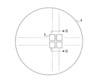
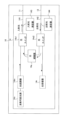
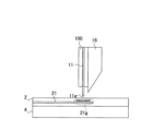
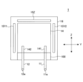
- FIG. 1 is a plan view of an optical element 2 that is an object to be measured by a light measurement device 1 according to a first embodiment of the present invention.
- FIG. 1 is a side view of a light measurement device 1 according to a first embodiment. 1 is a plan view seen through an optical element 2 that is a measurement target of a light measurement device 1 according to a first embodiment.
- FIG. 1 is a front view of a light measurement device 1 according to a first embodiment.
- 2 is a plan view of a light measurement unit 14 of the light measurement device 1 according to the first embodiment.
- FIG. 4 is a plan view of a light measurement unit 14 of the light measurement device 1 according to a first modified example of the first embodiment.
- FIG. 1 is a front view of a light measurement device 1
- FIG. 10 is a plan view of a light measurement unit 14 of a light measurement device 1 according to a second modified example of the first embodiment.
- FIG. FIG. 4 is a side view of a light measurement device 1 according to a second embodiment of the present invention.
- FIG. 11 is a side view of the light measurement device 1 according to a first modified example of the second embodiment.
- FIG. 11 is a side view of the light measurement device 1 according to a second modified example of the second embodiment.
- 11 is a transparent plan view of an optical element 2 that is a measurement target of a light measurement device 1 according to a third embodiment of the present invention.
- FIG. 13 is a plan view seen through an optical element 2 that is a measurement target of a light measurement device 1 according to a modified example of the third embodiment.
- FIG. 11 is a front view of a light measurement device 1 according to a fourth embodiment of the present invention.
- FIG. 11 is a side view of a light measurement device 1 according to a fourth embodiment of the present invention.
- FIG. 13 is a plan view of the light measurement device 1 according to a first modified example of the fourth embodiment of the present invention.
- 13 is a plan view of a light measurement unit 14 of a light measurement device 1 according to a third modified example of the first embodiment of the present invention.
- FIG. FIG. 13 is a plan view of a light measurement device 1 according to a sixth embodiment of the present invention.
- FIG. 13 is a plan view of the light measurement device 1 according to a modified example of the sixth embodiment of the present invention.
- FIG. 1 is a plan view of an optical element 2 that is an object to be measured by a light measurement device 1 according to a first embodiment of the present invention.
- multiple optical elements 2 are arranged on a wafer 4 at a predetermined interval.
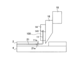
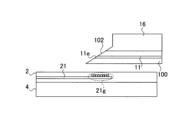
- FIG. 2 is a side view of the light measurement device 1 according to the first embodiment. However, FIG. 2 is also a cross-sectional view taken along line II-II in FIG. 1.
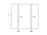
- FIG. 3 is a plan view seen through the optical element 2 that is the measurement target of the light measurement device 1 according to the first embodiment.
- FIG. 4 is a front view of the light measurement device 1 according to the first embodiment.
- the optical measurement device 1 includes an input optical probe 11, an output optical probe 12, a holding layer 100, an optical measurement unit 14, a substrate 16, and a stage 18. However, in FIG. 4, the stage 18 is omitted, and the holding layer 100 and the optical measurement unit 14 are shown in perspective.
- the optical measurement device 1 measures the incident light provided to the light receiving end 21e of the optical element 2 and the emitted light emitted from the emission end 22e of the optical element 2.
- the incident light probe 11 has an end 11e.
- the incident light probe 11 emits incident light at the end 11e, which is close to the light receiving end 21e.
- the emitting light probe 12 has an end 12e.
- the emitting light probe 12 receives the emitted light at end 12e, which is adjacent to the emitting end 22e. Note that in FIG. 2, the emitting light probe 12 is not shown because it has the same shape as the incident light probe 11 and is hidden by the incident light probe 11.
- the retention layer 100 retains the incident light probe 11 and the outgoing light probe 12.
- the incident light probe 11 and the outgoing light probe 12 penetrate the retention layer 100.
- the incident light probe 11 is bent.
- the incident light probe 11 is disposed to the side of the optical element 2. More specifically, in FIG. 2, the incident light probe 11 extends in the vertical direction and extends out from the retaining layer 100, but then bends at a right angle and extends to the left, with the end 11e of the incident light probe 11 disposed immediately adjacent to the light receiving end 21e of the optical element 2.
- the optical element 2 has optical waveguides 21 and 22.
- the optical waveguide 21 has a light receiving end 21e, which is exposed on the side of the optical element 2.
- the optical waveguide 22 has an emission end 22e, which is exposed on the side of the optical element 2.
- the optical waveguides 21 and 22 in the optical element 2 are shown as if they were cutting through the optical element 2 for the sake of convenience. However, the optical waveguides 21 and 22 do not necessarily cut through the optical element 2.
- the optical waveguides 21 and 22 in the optical element 2 are shown as if they cross the optical element 2 for convenience of illustration. However, the optical waveguides 21 and 22 do not need to cross the optical element 2 (this is also true for the other figures).
- FIG. 2 of the components in the optical measurement unit 14 only the input optical waveguide 141 is shown for convenience of illustration.
- FIG. 4 of the components in the optical measurement unit 14, only the input optical waveguide 141 and the output optical waveguide 142 are shown for convenience of illustration.
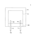
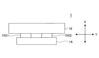
- FIG. 5 is a plan view of the light measurement unit 14 of the light measurement device 1 according to the first embodiment.
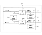
- the optical measurement unit 14 has an input optical waveguide 141, an output optical waveguide 142, an input optical meter 143, an output optical meter 144, an optical attenuator 14a, and optical switches 14s1 and 14s2.
- the incident light waveguide 141 provides incident light to the incident light probe 11.
- the output light waveguide 142 receives output light from the output light probe 12.
- the incident light meter 143 measures the incident light traveling through the incident light waveguide 141.
- the incident light meter 143 is, for example, an optical power monitor.
- the output light meter 144 measures the output light traveling through the output light waveguide 142.
- the output light meter 144 is, for example, an optical power monitor.
- Optical switch 14s1 is an optical switch that connects either the input from outside the optical measurement unit 14 or the output of optical attenuator 14a to the incident optical waveguide 141.
- Optical switch 14s2 is an optical switch that connects either the output to outside the optical measurement unit 14 or the input to the optical attenuator 14a to the output optical waveguide 142.
- the optical attenuator 14a receives the outgoing light traveling through the outgoing optical waveguide 142 via the optical switch 14s2, attenuates it, and provides it to the incoming optical waveguide 141 via the optical switch 14s1. As a result, the outgoing light is provided to the incoming optical waveguide 141 via the optical attenuator 14a.
- the input light probe 11, the output light probe 12, and the light measurement unit 14 are arranged on the same substrate 16.
- the substrate 16 is, for example, a silicon substrate.
- the input light probe 11 and the input light waveguide 141 are directly connected, and the output light probe 12 and the output light waveguide 142 are directly connected.
- the substrate 16 is fixed to the stage 18.
- the stage 18 can be moved in two orthogonal directions within the plane of FIG. 2 and in a direction orthogonal to the plane of FIG. 2 (e.g., the XYZ directions), thereby allowing the input light probe 11 and output light probe 12 to be moved together with the substrate 16.
- the end 11e of the input optical probe 11 is placed immediately adjacent to the light receiving end 21e of the optical element 2. Then, the end 12e of the output optical probe 12 is placed immediately adjacent to the output end 22e of the optical element 2.
- an input (incident light) from outside the light measurement unit 14 is provided to the incident light waveguide 141 via the optical switch 14s1.
- the incident light is measured by the incident light measuring device 143.
- the incident light is provided from the incident light waveguide 141 to the incident light probe 11, is emitted from the end 11e of the incident light probe 11, and is received by the light receiving end 21e of the optical element 2.
- the optical element 2 emits the emitted light from the emission end 22e.
- the emitted light emitted from the emission end 22e of the optical element 2 is received by the end 12e of the emitting light probe 12.
- the output light received by the end 12e of the output light probe 12 passes through the output light probe 12 and is provided to the output light waveguide 142.
- the output light traveling through the output light waveguide 142 is measured by the output light measuring device 144.
- the output light traveling through the output light waveguide 142 is output to the outside of the light measuring unit 14.
- the output light traveling through the output light waveguide 142 is provided as input light to the input light waveguide 141 via the optical switch 14s2, the optical attenuator 14a, and the optical switch 14s1.
- the incident optical probe 11, the output optical probe 12, and the optical measurement unit 14 are arranged on the same substrate 16. Therefore, the incident optical probe 11 and the input optical waveguide 141 can be directly connected, and the output optical probe 12 and the output optical waveguide 142 can be directly connected. This makes it possible to reduce the loss of light between the incident optical probe 11 and the output optical probe 12 and the optical measurement unit 14.
- FIG. 6 is a plan view of the light measurement unit 14 of the light measurement device 1 according to a first modification of the first embodiment.
- the optical measurement unit 14 of the optical measurement device 1 according to the first modification of the first embodiment further includes a wavelength-tunable light source 14v, an optical modulator 14m, and an optical receiver 14r in addition to the components described in the first embodiment.
- the optical modulator 14m modulates the output of the tunable light source 14v and provides it to the input optical waveguide 141 via the optical switch 14s1.
- the optical receiver 14r receives the emitted light traveling through the output optical waveguide 142 via the optical switch 14s2.
- FIG. 7 is a plan view of the light measurement section 14 of the light measurement device 1 according to a second modification of the first embodiment.
- the light measurement unit 14 of the light measurement device 1 according to the second modification of the first embodiment further includes a multi-wavelength light source 14mw and a light source light measurement device 146 in addition to the components described in the first embodiment.
- the light measurement unit 14 of the light measurement device 1 according to the second modified example of the first embodiment has a multi-wavelength light source 14mw.
- the multi-wavelength light source 14mw provides incident light to the light receiving end (not shown, but separate from the light receiving end 21e) via the incident light waveguide 145 and the incident light probe 13.
- the light source optical meter 146 measures the incident light emitted from the multi-wavelength light source 14mw and traveling through the incident light waveguide 145.
- the light source optical meter 146 is, for example, an optical power monitor.
- FIG. 16 is a plan view of the light measurement unit 14 of the light measurement device 1 according to a third modification of the first embodiment.
- the optical measurement unit 14 of the optical measurement device 1 according to the third modified example of the first embodiment is obtained by removing the optical attenuator 14a and the optical switches 14s1 and 14s2 from the optical measurement unit 14 of the first embodiment. As a result, the output light traveling through the output optical waveguide 142 is provided to the input optical waveguide 141.
- the optical measurement device 1 according to the second embodiment differs from the first embodiment in that the input optical probe 11 or the output optical probe 12 is arranged above the optical element 2, in that the input optical probe 11 or the output optical probe 12 is arranged to the side of the optical element 2.
- FIG. 8 is a side view of the light measurement device 1 according to the second embodiment of the present invention.
- parts similar to those in the first embodiment are given the same reference numerals and will not be described.
- the incident light probe 11 is bent.
- the incident light probe 11 is disposed above the optical element 2. More specifically, in FIG. 8, the incident light probe 11 extends in the left-right direction and protrudes outside the retention layer 100, but then bends at a right angle and extends straight down, with the end 11e of the incident light probe 11 being disposed immediately above the grating coupler 21g of the optical element 2.
- the operation of the second embodiment is similar to that of the first embodiment, and a description thereof will be omitted.
- the second embodiment also provides the same effects as the first embodiment.
- FIG. 9 is a side view of the light measurement device 1 according to a first modification of the second embodiment.
- the incident optical probe 11 is linear.
- the incident optical probe 11 is disposed above the optical element 2, as in the second embodiment.
- the incident optical probe 11 extends in the vertical direction and extends outside the retention layer 100, with the end 11e of the incident optical probe 11 being disposed immediately above the grating coupler 21g of the optical element 2.
- FIG. 10 is a side view of the light measurement device 1 according to a second modification of the second embodiment.
- the incident light probe 11 is linear.
- the incident light probe 11 is disposed above the optical element 2, as in the second embodiment.
- the end 11e of the incident light probe 11 is disposed on the reflecting member 102 without going outside the holding layer 100.
- the incident light emitted from the end 11e is reflected by the reflecting member 102 and provided to the grating coupler 21g.
- the incident light probe 11 emits light via the reflecting member 102.
- the emitting light probe 12 also receives light via the reflecting member 102.
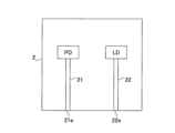
- a light measurement device 1 according to a third embodiment differs from the first embodiment in that the optical element 2 has a photodetector PD and a light source LD.
- FIG. 11 is a plan view showing the optical element 2 that is the measurement target of the optical measurement device 1 according to the third embodiment of the present invention.
- parts similar to those in the first embodiment are given the same reference numerals and will not be described.
- the optical element 2 has a photodetector PD and a light source LD.
- the photodetector PD is, for example, an optical power monitor, and is connected to the light receiving end 21e via the optical waveguide 21.
- the light source LD is connected to the light emitting end 22e via the optical waveguide 22. It is assumed that the power of the light output by the light source LD is known.
- the end 11e of the input optical probe 11 is placed immediately adjacent to the light receiving end 21e of the optical element 2. Then, the end 12e of the output optical probe 12 is placed immediately adjacent to the output end 22e of the optical element 2.
- an input (incident light) from outside the light measurement unit 14 is provided to the incident light waveguide 141 via the optical switch 14s1.
- the incident light is measured by the incident light meter 143.
- the incident light is provided from the incident light waveguide 141 to the incident light probe 11, radiated from the end 11e of the incident light probe 11, and received by the light receiving end 21e of the optical element 2.
- the received light is provided to the photodetector PD via the optical waveguide 21, and measured by the photodetector PD.
- the optical element 2 emits the emitted light from the emission end 22e.
- the emitted light emitted from the emission end 22e of the optical element 2 is received by the end 12e of the emitting light probe 12.
- the output light received by the end 12e of the output light probe 12 passes through the output light probe 12 and is provided to the output light waveguide 142.
- the output light traveling through the output light waveguide 142 is measured by the output light measuring device 144.
- the output light traveling through the output light waveguide 142 is output to the outside of the light measuring unit 14.
- the output light traveling through the output light waveguide 142 is provided as input light to the input light waveguide 141 via the optical switch 14s2, the optical attenuator 14a, and the optical switch 14s1.
- the third embodiment also provides the same effects as the first embodiment.
- the third embodiment it is possible to know whether the input light waveguide 141, the output light waveguide 142, the input light probe 11, and the output light probe 12 are operating normally. This adds a diagnostic function to the light probe.
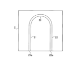
- FIG. 12 is a transparent plan view of the optical element 2 that is the measurement target of the light measurement device 1 according to a modification of the third embodiment.
- the optical element 2 in the modified example of the third embodiment has a connection portion 23 that connects the light receiving end 21e and the light emitting end 22e.
- the end 11e of the input optical probe 11 is placed immediately adjacent to the light receiving end 21e of the optical element 2. Then, the end 12e of the output optical probe 12 is placed immediately adjacent to the output end 22e of the optical element 2.
- an input (incident light) from outside the light measurement unit 14 is provided to the incident light waveguide 141 via the optical switch 14s1.
- the incident light is measured by the incident light meter 143.
- the incident light is provided from the incident light waveguide 141 to the incident light probe 11, emitted from the end 11e of the incident light probe 11, and received by the light receiving end 21e of the optical element 2.
- the received light passes through the optical waveguide 21, the connection portion 23, and the optical waveguide 22, and is emitted from the emission end 22e.
- the emitted light from the emission end 22e of the optical element 2 is received by the end 12e of the emission light probe 12.
- the output light received by the end 12e of the output light probe 12 passes through the output light probe 12 and is provided to the output light waveguide 142.
- the output light traveling through the output light waveguide 142 is measured by the output light measuring device 144.
- the output light traveling through the output light waveguide 142 is output to the outside of the light measuring unit 14.
- the output light traveling through the output light waveguide 142 is provided as input light to the input light waveguide 141 via the optical switch 14s2, the optical attenuator 14a, and the optical switch 14s1.
- the light measurement device 1 may also have both the photodetector PD and the light source LD (third embodiment: FIG. 11) and the connection portion 23 (variant of the third embodiment: FIG. 12).
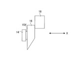
- the light measurement device 1 according to the fourth embodiment differs from the first embodiment in that it includes actuators 15Y1, 15Y2, 15Z, 15X, 15X1, and 15X2 that move the input light probe 11 and the output light probe 12.
- FIG. 13 is a front view of the optical measurement device 1 according to the fourth embodiment of the present invention.
- FIG. 14 is a side view of the optical measurement device 1 according to the fourth embodiment of the present invention.
- the optical measurement device 1 includes actuators 15Y1, 15Y2, 15Z, and 15X that move the input optical probe 11 and the output optical probe 12.
- Actuators 15Y1, 15Y2, 15Z, and 15X are arranged on a substrate 16.
- actuators 15Y1 and 15Y2 are disposed on the left and right of light measurement unit 14.
- Actuators 15Y1 and 15Y2 are, for example, well-known comb actuators. Actuators 15Y1 and 15Y2 can move light measurement unit 14 in the Y-axis direction.
- Actuator 15Z is disposed above light measurement unit 14. Actuator 15Z is, for example, a well-known comb actuator. Actuator 15Z can move light measurement unit 14 in the Z-axis direction.
- the actuator 15X is disposed between the light measurement unit 14 and the substrate 16.
- the actuator 15X is, for example, a well-known piezoelectric actuator. When a voltage is applied to the actuator 15X, it contracts or expands in the X-axis direction. This allows the light measurement unit 14 to move in the X-axis direction.
- the fourth embodiment also provides the same effects as the first embodiment.
- the light measurement unit 14 can be moved more minutely than the stage 18.
- the light measurement device 1 is a plan view of a light measurement device 1 according to a first modification of the fourth embodiment of the present invention.
- the light measurement device 1 according to the modification of the fourth embodiment includes actuators 15X1 and 15X2 instead of the actuator 15X.
- actuators 15X1 and 15X2 are disposed between light measurement unit 14 and substrate 16, spaced apart from each other in the Y-axis direction.
- Actuators 15X1 and 15X2 are, for example, well-known piezoelectric actuators.
- the light measurement unit 14 can be rotated around the direction perpendicular to the paper surface of FIG. 15 (Z direction) as the rotation axis. Note that by appropriately arranging two actuators in this way, and contracting one and expanding the other, the light measurement unit 14 can be rotated around any axis.
- Second Modification By moving the end 12e of the emitted light probe 12 by the actuators 15X (or 15X1, 15X2), 15Y1, 15Y2 and 15Z so that the measurement result (optical power) of the emitted light measuring instrument 144 becomes a predetermined value (e.g., maximum), the emission end 22e can be aligned with the end 12e.
- a predetermined value e.g., maximum
- this adds a centering function for the optical probe.
- the fifth embodiment describes various calibrations using the light measurement device 1 according to the third embodiment.
- the photodetector PD is calibrated (valued) so that the measurement results of the photodetector PD match the measurement results of the optical power monitor, which can measure accurately. However, there must be no loss at the light receiving end 21e.
- the incident light is measured by the photodetector PD, as in the third embodiment.
- the photodetector PD is assumed to be calibrated as described in (1) above. Furthermore, there is no loss at the light receiving end 21e.
- the incident light meter 143 is calibrated so that the measurement results of the incident light meter 143 match the measurement results of the photodetector PD.
- the optical element 2 emits emitted light from the emission end 22e.
- the emitted light emitted from the emission end 22e of the optical element 2 is received by the end 12e of the emitted light probe 12.
- the emitted light is measured by the emitted light measuring instrument 144, as in the third embodiment.
- loss due to the optical attenuator 14a is kept to a minimum.
- the emitted light is provided as incident light to the incident light waveguide 141. This incident light is measured by the incident light measuring device 143.
- the exit light meter 144 is calibrated so that the measurement results of the exit light meter 144 match the measurement results of the incident light meter 143.
- the incident light meter 143 has been calibrated as described in (2) above.
- the loss due to optical switches 14s1, 14s2 and optical attenuator 14a can be found by taking the difference between the measurement result of the above incident light meter 143 and the measurement result of the incident light meter 143 when the optical switches 14s1, 14s2 and optical attenuator 14a are removed and the incident light waveguide 141 and the output light waveguide 142 are directly connected.
- the output light meter 144 may be calibrated so that the value obtained by subtracting this loss (which may be replaced with the loss due to a typical optical switch and optical attenuator) from the measurement result of the output light meter 144 matches the measurement result of the incident light meter 143.
- the light source LD of a certain optical element 2 is calibrated based on the measurement results of the photodetector PD of another optical element 2. Note that once the calibration of the light source LD and the calibration of the emitted light measuring instrument 144 have been completed, the coupling loss of the emitted light probe 12 can be obtained.
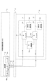
- the optical measurement device 1 according to the sixth embodiment differs from the first embodiment in that the connection state of the optical connector 19 is determined.
- FIG. 17 is a plan view of the optical measurement device 1 according to the sixth embodiment of the present invention.
- the optical measurement device 1 according to the sixth embodiment is obtained by adding a probe card 17 and an optical connector 19 to the optical measurement device 1 according to the first embodiment.
- a substrate 16 is disposed on the probe card 17.
- An optical connector 19 is disposed on the probe card 17 and is connected to the input optical waveguide 141 via an optical switch 14s1.
- semiconductor test equipment (ATE: Automated Test Equipment) 4 is connected to the optical connector 19.
- the semiconductor test device 4 has a measuring device 42 and an optical connector 44.
- the measuring device 42 has a laser 42a that emits laser light and an optical power meter 42b that measures the power of the received light.
- the optical connector 44 is connected to the measuring device 42 and the optical connector 19.
- Laser light of known optical power emitted from laser 42a is provided to the optical measurement device 1 via optical connector 44 and optical connector 19. This laser light is further provided as incident light to the incident light waveguide 141 via optical switch 14s1. This incident light (i.e., the input from optical connector 19) is measured by the incident light meter 143.
- connection state of the optical connector 19 can be determined.
- FIG. 18 is a plan view of the light measurement device 1 according to a modification of the sixth embodiment of the present invention.
- the optical connector 19 is disposed on the probe card 17 and is connected to the input optical waveguide 141 via the optical switch 14s1. Furthermore, the optical connector 19 is connected to the output optical waveguide 142 via the optical switch 14s2.
- optical connector 19 The input from optical connector 19 is output from optical connector 19 via optical switches 14s1 and 14s2.
- the output from the optical connector 19 is measured by the optical power meter 42b. Based on the measurement results, it is determined whether the connection state of the optical connector 19 is good or not.
Landscapes
- Chemical & Material Sciences (AREA)
- Analytical Chemistry (AREA)
- Physics & Mathematics (AREA)
- General Physics & Mathematics (AREA)
- Photometry And Measurement Of Optical Pulse Characteristics (AREA)
- Testing Of Optical Devices Or Fibers (AREA)
Abstract
La présente invention réduit la perte de lumière entre une sonde optique et une partie de mesure optique. Un dispositif de mesure optique (1) mesure la lumière incidente appliquée à l'extrémité de réception de lumière (21e) d'un élément optique (2) et la lumière émise émise par l'extrémité d'émission (22e) de l'élément optique (2). Le dispositif de mesure optique (1) comprend une sonde optique incidente (11) qui est proche de l'extrémité de réception de lumière (21e) et émet une lumière incidente, une sonde optique d'émission (12) qui est proche de l'extrémité d'émission (22e) et reçoit la lumière émise, un guide d'ondes optique incident (141) qui applique une lumière incidente à la sonde optique incidente (11), un guide d'ondes optique d'émission (142) qui reçoit la lumière émise par la sonde optique d'émission (12), un instrument de mesure de lumière incidente (143) qui mesure la lumière incidente se déplaçant à travers le guide d'ondes optique incident (141), et une partie de mesure optique (14) qui présente un instrument de mesure de lumière émis (144) qui mesure la lumière émise se déplaçant à travers le guide d'ondes optique d'émission (142). La sonde optique incidente (11), la sonde optique d'émission (12) et la partie de mesure optique (14) sont disposées sur le même substrat (16). La sonde optique incidente (11) et le guide d'ondes optique incident (141) sont directement connectés. La sonde optique d'émission (12) et le guide d'ondes optique d'émission (142) sont directement connectés.
Priority Applications (3)
| Application Number | Priority Date | Filing Date | Title |
|---|---|---|---|
| PCT/JP2023/029888 WO2025041201A1 (fr) | 2023-08-18 | 2023-08-18 | Dispositif de mesure optique |
| CN202380100324.XA CN121488145A (zh) | 2023-08-18 | 2023-08-18 | 光测量装置 |
| TW113112531A TW202509484A (zh) | 2023-08-18 | 2024-04-02 | 光測定裝置 |
Applications Claiming Priority (1)
| Application Number | Priority Date | Filing Date | Title |
|---|---|---|---|
| PCT/JP2023/029888 WO2025041201A1 (fr) | 2023-08-18 | 2023-08-18 | Dispositif de mesure optique |
Publications (1)
| Publication Number | Publication Date |
|---|---|
| WO2025041201A1 true WO2025041201A1 (fr) | 2025-02-27 |
Family
ID=94731703
Family Applications (1)
| Application Number | Title | Priority Date | Filing Date |
|---|---|---|---|
| PCT/JP2023/029888 Pending WO2025041201A1 (fr) | 2023-08-18 | 2023-08-18 | Dispositif de mesure optique |
Country Status (3)
| Country | Link |
|---|---|
| CN (1) | CN121488145A (fr) |
| TW (1) | TW202509484A (fr) |
| WO (1) | WO2025041201A1 (fr) |
Citations (7)
| Publication number | Priority date | Publication date | Assignee | Title |
|---|---|---|---|---|
| JP2006324588A (ja) * | 2005-05-20 | 2006-11-30 | Sharp Corp | 受光素子検査方法及び受光素子検査装置 |
| JP2011242208A (ja) * | 2010-05-17 | 2011-12-01 | Advantest Corp | 試験装置及び試験方法 |
| WO2014034655A1 (fr) * | 2012-08-31 | 2014-03-06 | 日本電気株式会社 | Sonde optique, dispositif et procédé d'inspection |
| JP2020106736A (ja) * | 2018-12-28 | 2020-07-09 | 日本電信電話株式会社 | 光検査回路 |
| JP2020530121A (ja) * | 2017-08-07 | 2020-10-15 | イエーノプティーク オプティカル システムズ ゲーエムベーハー | 光電子チップを接触させるための位置公差に無感応な接触モジュール |
| US20210199691A1 (en) * | 2019-12-30 | 2021-07-01 | Juniper Networks, Inc. | Compact opto-electric probe |
| JP2023520159A (ja) * | 2020-03-26 | 2023-05-16 | 株式会社アドバンテスト | 高周波コンポーネント、とくには検査対象シリコンフォトニクスデバイスを検査するための検査装置 |
-
2023
- 2023-08-18 WO PCT/JP2023/029888 patent/WO2025041201A1/fr active Pending
- 2023-08-18 CN CN202380100324.XA patent/CN121488145A/zh active Pending
-
2024
- 2024-04-02 TW TW113112531A patent/TW202509484A/zh unknown
Patent Citations (7)
| Publication number | Priority date | Publication date | Assignee | Title |
|---|---|---|---|---|
| JP2006324588A (ja) * | 2005-05-20 | 2006-11-30 | Sharp Corp | 受光素子検査方法及び受光素子検査装置 |
| JP2011242208A (ja) * | 2010-05-17 | 2011-12-01 | Advantest Corp | 試験装置及び試験方法 |
| WO2014034655A1 (fr) * | 2012-08-31 | 2014-03-06 | 日本電気株式会社 | Sonde optique, dispositif et procédé d'inspection |
| JP2020530121A (ja) * | 2017-08-07 | 2020-10-15 | イエーノプティーク オプティカル システムズ ゲーエムベーハー | 光電子チップを接触させるための位置公差に無感応な接触モジュール |
| JP2020106736A (ja) * | 2018-12-28 | 2020-07-09 | 日本電信電話株式会社 | 光検査回路 |
| US20210199691A1 (en) * | 2019-12-30 | 2021-07-01 | Juniper Networks, Inc. | Compact opto-electric probe |
| JP2023520159A (ja) * | 2020-03-26 | 2023-05-16 | 株式会社アドバンテスト | 高周波コンポーネント、とくには検査対象シリコンフォトニクスデバイスを検査するための検査装置 |
Also Published As
| Publication number | Publication date |
|---|---|
| CN121488145A (zh) | 2026-02-06 |
| TW202509484A (zh) | 2025-03-01 |
Similar Documents
| Publication | Publication Date | Title |
|---|---|---|
| US10345233B2 (en) | Optical measuring device having photonic chip with interferometer and phase adjuster set for minimizing signal from interference region | |
| US5341205A (en) | Method for characterization of optical waveguide devices using partial coherence interferometry | |
| JP6358092B2 (ja) | 光プローブ、検査装置、検査方法 | |
| JP5778078B2 (ja) | 物体をモニタする干渉計システム | |
| US8335411B2 (en) | Fiber optic bi-directional coupling lens | |
| JP6204272B2 (ja) | 距離計測装置 | |
| CN114222929A (zh) | 供lidar芯片使用的lidar适配器 | |
| JP5621837B2 (ja) | 電界/磁界プローブ | |
| WO2009099090A1 (fr) | Dispositif de mesure de champ électromagnétique | |
| JP2023553579A (ja) | Lidarシステムにおける信号対ノイズ比の向上 | |
| EP2718666A1 (fr) | Systèmes confocaux à multiples longueurs d'onde couplées pour mesurer des distances | |
| CN111201427B (zh) | 反射光测定装置 | |
| WO2025041201A1 (fr) | Dispositif de mesure optique | |
| EP4575445A1 (fr) | Sonde optique et procédés associés | |
| US10209278B2 (en) | Sensor unit | |
| US20210026017A1 (en) | Apparatus for ascertaining a distance to an object | |
| US20120316830A1 (en) | Coupled multi-wavelength confocal systems for distance measurements | |
| JP4027352B2 (ja) | 光ファイバプローブ装置 | |
| US20120314200A1 (en) | Coupled multi-wavelength confocal systems for distance measurements | |
| JP2002250675A (ja) | 低コヒーレントリフレクトメータ | |
| JP4802916B2 (ja) | 双方向光モジュールおよびこれを用いた光パルス試験器 | |
| KR100343813B1 (ko) | 광섬유나 광도파로 표면의 굴절률구조 측정장치 및 방법 | |
| JP3455615B2 (ja) | 反射波長測定方法及び装置、光線路識別方法及びシステム | |
| US20240118167A1 (en) | Circuit, Device and Method for Optical Characteristic Inspection | |
| WO2025135086A1 (fr) | Procédé d'inspection de puce de circuit optique à l'aide d'une machine de test de plc, et puce de circuit optique |
Legal Events
| Date | Code | Title | Description |
|---|---|---|---|
| 121 | Ep: the epo has been informed by wipo that ep was designated in this application |
Ref document number: 23949663 Country of ref document: EP Kind code of ref document: A1 |
|
| NENP | Non-entry into the national phase |
Ref country code: DE |