WO2025028381A1 - アルミニウム配線材及びその製造方法 - Google Patents
アルミニウム配線材及びその製造方法 Download PDFInfo
- Publication number
- WO2025028381A1 WO2025028381A1 PCT/JP2024/026568 JP2024026568W WO2025028381A1 WO 2025028381 A1 WO2025028381 A1 WO 2025028381A1 JP 2024026568 W JP2024026568 W JP 2024026568W WO 2025028381 A1 WO2025028381 A1 WO 2025028381A1
- Authority
- WO
- WIPO (PCT)
- Prior art keywords
- wiring material
- less
- aluminum wiring
- ratio
- aluminum
- Prior art date
- Legal status (The legal status is an assumption and is not a legal conclusion. Google has not performed a legal analysis and makes no representation as to the accuracy of the status listed.)
- Pending
Links
Images


Classifications
-
- C—CHEMISTRY; METALLURGY
- C22—METALLURGY; FERROUS OR NON-FERROUS ALLOYS; TREATMENT OF ALLOYS OR NON-FERROUS METALS
- C22C—ALLOYS
- C22C21/00—Alloys based on aluminium
-
- C—CHEMISTRY; METALLURGY
- C22—METALLURGY; FERROUS OR NON-FERROUS ALLOYS; TREATMENT OF ALLOYS OR NON-FERROUS METALS
- C22F—CHANGING THE PHYSICAL STRUCTURE OF NON-FERROUS METALS AND NON-FERROUS ALLOYS
- C22F1/00—Changing the physical structure of non-ferrous metals or alloys by heat treatment or by hot or cold working
-
- C—CHEMISTRY; METALLURGY
- C22—METALLURGY; FERROUS OR NON-FERROUS ALLOYS; TREATMENT OF ALLOYS OR NON-FERROUS METALS
- C22F—CHANGING THE PHYSICAL STRUCTURE OF NON-FERROUS METALS AND NON-FERROUS ALLOYS
- C22F1/00—Changing the physical structure of non-ferrous metals or alloys by heat treatment or by hot or cold working
- C22F1/04—Changing the physical structure of non-ferrous metals or alloys by heat treatment or by hot or cold working of aluminium or alloys based thereon
-
- H—ELECTRICITY
- H01—ELECTRIC ELEMENTS
- H01B—CABLES; CONDUCTORS; INSULATORS; SELECTION OF MATERIALS FOR THEIR CONDUCTIVE, INSULATING OR DIELECTRIC PROPERTIES
- H01B1/00—Conductors or conductive bodies characterised by the conductive materials; Selection of materials as conductors
- H01B1/02—Conductors or conductive bodies characterised by the conductive materials; Selection of materials as conductors mainly consisting of metals or alloys
-
- H—ELECTRICITY
- H01—ELECTRIC ELEMENTS
- H01B—CABLES; CONDUCTORS; INSULATORS; SELECTION OF MATERIALS FOR THEIR CONDUCTIVE, INSULATING OR DIELECTRIC PROPERTIES
- H01B5/00—Non-insulated conductors or conductive bodies characterised by their form
- H01B5/02—Single bars, rods, wires, or strips
-
- H—ELECTRICITY
- H10—SEMICONDUCTOR DEVICES; ELECTRIC SOLID-STATE DEVICES NOT OTHERWISE PROVIDED FOR
- H10W—GENERIC PACKAGES, INTERCONNECTIONS, CONNECTORS OR OTHER CONSTRUCTIONAL DETAILS OF DEVICES COVERED BY CLASS H10
- H10W72/00—Interconnections or connectors in packages
- H10W72/071—Connecting or disconnecting
Definitions
- the present invention relates to aluminum wiring material, particularly conductive aluminum wiring material that has excellent bonding reliability at high temperatures, excellent followability during bonding, and high strength against vibration, and a method for manufacturing the same.
- aluminum wiring materials have been used as wiring materials to connect the electrodes and bus bars of lithium-ion batteries and as bonding wiring materials for power semiconductors.
- Lithium-ion batteries are used as drive batteries (power sources) in hybrid vehicles (HVs), plug-in hybrid vehicles (PHVs, PHEVs), and electric vehicles.
- Hybrid vehicles and plug-in hybrid vehicles are driven by a gasoline engine and an electric motor. Electric vehicles are driven only by an electric motor.
- Hybrid vehicles and electric vehicles run by driving an electric motor with electricity stored in the lithium-ion battery.
- drive batteries other than lithium-ion batteries include lead-acid batteries and nickel-metal hydride batteries, but because lithium-ion batteries are light, small, high-output, and have a long lifespan, they are increasingly being used in electric vehicles that prioritize fuel efficiency.
- Cylindrical batteries are often used as lithium batteries for the drive batteries of electric vehicles because they are small, have a stable shape, and are easy to replace. Cylindrical batteries have a structure in which an electrolyte solution is sealed in a cylindrical metal case.
- a battery pack using cylindrical batteries consists, for example, of an outer case to which lead members (bus bars) are connected, multiple cylindrical batteries housed in the outer case, and wiring material that connects the electrodes of the cylindrical batteries to the lead members.
- Aluminum wiring material made of an aluminum alloy is widely used as the wiring material for these cylindrical batteries because it is advantageous in terms of conductivity and cost.
- Power semiconductors are also called power chips, power semiconductors, power devices, power elements, and power semiconductor elements. Power semiconductors are composed of power chips and bonding wiring materials that connect the power chips to each other and to external electrodes. Power semiconductors are responsible for driving motors, charging batteries, and supplying power to operate microcontrollers and large-scale integrated circuits (LSIs).
- the main power chips used in the transportation field, such as automobiles, are insulated gate bipolar transistors (IGBTs) and metal oxide semiconductor field effect transistors (MOSFETs), which are suitable for high power.
- IGBTs insulated gate bipolar transistors
- MOSFETs metal oxide semiconductor field effect transistors
- bonding wiring materials for power semiconductors relatively thick aluminum wiring materials with wire diameters of 40 ⁇ m to 700 ⁇ m are often used to pass large currents.
- a power supply circuit that combines multiple power semiconductors and is integrated into one package is called a "power module.”
- a common method is to hold the tip of the wiring material with a gripping device called a wedge tool (sometimes simply called a "tool"), and while applying ultrasonic waves to the wiring material, press the wiring material together with the wedge tool against a lead material or electrode, crushing and deforming it, thereby joining the lead material or electrode to the wiring material.
- a wedge tool sometimes simply called a "tool”
- Electric vehicles are used in a variety of external environments, including cold regions, tropical regions, and regions with high humidity and salt. For example, when an electric vehicle is driven in cold or tropical regions, it is exposed to low and high temperatures and these temperature changes for long periods of time.
- the power modules and drive batteries installed in electric vehicles, as well as the aluminum wiring materials connected to them are required to be compatible with all possible environments in which electric vehicles will be used, such as those mentioned above.
- the power module and drive battery of an electric vehicle are also subject to temperature changes due to heating and cooling caused by electric current.
- An electric vehicle repeats a cycle of stopping the current when it is stopped and starting the current when it starts driving.
- the power chip heats up and becomes hot due to the current, and cools down rapidly when the current is stopped.
- the aluminum wiring material bonded to the power chip and drive battery is also exposed to a temperature cycle of heating and cooling.
- the accelerator and brake are frequently repeated, and this temperature cycle of heating and cooling is also frequently repeated.
- thermal stress is generated due to the difference in the thermal expansion coefficient between the power chip and the aluminum wiring material, which can cause metal fatigue in the joint between the power chip and the aluminum wiring material and in the aluminum wiring material.
- the possibility of peeling or breaking of the joint and the possibility of cracks occurring in the aluminum wiring material increase. Therefore, there has been a demand for an aluminum wiring material that can demonstrate long-term reliability of the joint even when such a temperature cycle of heating and cooling is repeated.
- power transistors a type of power semiconductor
- Inverters are installed in energy-saving (hereafter also referred to as "energy-saving") home appliances such as air conditioners, refrigerators, and washing machines.
- the power transistor switches the current on and off, and the inverter controls the rotation speed of the motor that drives the home appliance.
- energy-saving energy-saving
- By using an inverter it is possible to reduce unnecessary motor movement and achieve energy savings, while, for example, in an air conditioner, it is possible to maintain a stable room temperature.
- a temperature cycle of heating and cooling of the wiring material is repeated by turning on and off the current.
- Patent Document 1 is "an aluminum alloy thin wire for ultrasonic bonding of semiconductor devices, which consists of 0.2 to 2.0 mass % iron (Fe) and the remainder being aluminum (Al) with a purity of 99.99 mass % or more, characterized in that iron (Fe) is dissolved in the aluminum (Al) matrix of the aluminum alloy thin wire at 0.01 to 0.05%, and the wiredrawing matrix structure in the cross section of the aluminum alloy thin wire is a homogeneous fine recrystallized structure on the order of several ⁇ m, with iron (Fe)-aluminum (Al) intermetallic compound particles uniformly crystallized at the interface and inner surface of the structure.”
- Patent Document 1 describes how, by adding a solution treatment and rapid cooling process before the thermal refining treatment, the amount of iron (Fe) dissolved in the aluminum (Al) matrix is increased to 0.052%, which is the solid solubility limit at 650°C, and then normal continuous cold wire drawing and thermal refining treatment are performed to refine the crystal grain size of
- Patent Document 2 is "an aluminum alloy wire for ultrasonic bonding with an aluminum pad of a semiconductor element, the wire being made of 0.01-0.2 mass% iron (Fe), 1-20 mass ppm silicon (Si), and the remainder being a high-purity aluminum (Al) alloy, the aluminum alloy wire being an alloy made of 0.01-0.2 mass% iron (Fe), 1-20 mass ppm silicon (Si), and the remainder being aluminum (Al) with a purity of 99.997 mass% or more, the amount of Fe in solid solution being 0.01-0.06%, the amount of Fe precipitated being 7 times or less the amount of Fe in solid solution, and the wire has a fine structure with an average crystal grain size of 6-12 ⁇ m.”
- Patent Document 2 describes how the recrystallization temperature is stabilized by maintaining the ratio of the amount of Fe precipitated to the amount of Fe in solid solution within a certain range, and how the strength is improved by adding a small amount of Si, resulting in stabilization of the thermal shock test results (see paragraph 0012 of the thermal
- Patent Document 3 is characterized in that "it is made of Al or an Al alloy, has an average crystal grain size of 0.01 to 50 ⁇ m in a cross section perpendicular to the axis of the wiring, and is characterized in that, when the crystal orientation is measured on the cross section perpendicular to the axis of the wiring, the orientation ratio of the crystal orientation ⁇ 111>, which has an angle difference of 15° or less with respect to the longitudinal direction of the wiring, among the crystal orientations in the longitudinal direction of the wiring, is 30 to 90%.”
- Patent Document 3 also describes that the reliability of the joints in the semiconductor device after long-term operation at high temperatures can be ensured even when the semiconductor device is used continuously for long periods of time in a high-temperature environment (see paragraph 0012 of the specification).
- Patent Document 4 The invention described in Patent Document 4 is characterized by "containing, by mass%, 0.02-1% Fe, 0.05-0.5% total of at least one of Mn and Cr, the remainder being Al and unavoidable impurities, and the total of the dissolved amounts of Fe, Mn, and Cr being 0.01-1%.”
- Patent Document 4 describes that by containing a predetermined amount of one or both of Mn and Cr in addition to Fe, and by setting the total of the dissolved amounts of Fe, Mn, and Cr to 0.01-1% in the solution heat treatment and subsequent quenching treatment, the recrystallization temperature of the wire is increased, and the progress of recrystallization of the bonding wire can be sufficiently suppressed and a decrease in the strength of the wire can be prevented even when the semiconductor device is used continuously for a long period of time in a high-temperature environment (see paragraph 0014 of the specification).
- the area ratio of crystals in which the angle difference between the crystal ⁇ 111> orientation and the longitudinal direction of the wire is within 15° is preferably 30 to 90%, and that this allows recrystallization to proceed appropriately due to the thermal refining treatment during wire drawing, softening the wire, and preventing chip cracking during bonding and reduced bondability of the joint (see paragraph 0026 of the same specification).
- Patent Document 5 is "an aluminum wire made of an aluminum alloy with an aluminum purity of 99% by mass or more, containing a total of 0.01% by mass or more and 1% by mass or less of iron and silicon relative to the total amount of the aluminum alloy, and characterized in that the (111) orientation index is 1 or more and the (200) orientation index is 1 or less in a cross section perpendicular to the wire axis of the aluminum wire, and the area ratio of precipitated particles is 0.02% to 2% or less.”
- Patent Document 5 describes that by containing a predetermined amount of iron and silicon and making the (111) orientation index 1 or more and the (200) orientation index 1 or less in a cross section perpendicular to the wire axis, a long life is achieved in a power cycle test (see paragraph 0044 of the specification), and further, by making the area ratio of precipitated particles 0.02% to 2% or less, it is possible to prevent the wire from coming off the wedge tool during bonding wire bonding for power semiconductors (see paragraph 0050 of the
- Reducing the wiring resistance in semiconductor packages is also important in terms of energy conservation in electric vehicles and home appliances.
- the wiring resistance i.e. the power consumed by the electrical resistance of aluminum wiring material
- it is effective to reduce the length of the wiring material by joining the loop with a low height (low loop) and short loop length (short loop).
- the loop height here refers to the height from the lowest point of the wiring material joint to the highest point of the loop
- the loop length refers to the straight-line distance between both ends of the first joint and the second joint.
- the conventional wiring materials aimed at long-term reliability tend to have higher strength, while the stronger the wiring material, the poorer the vibration resistance. This is because the vibration resistance is improved by increasing the elongation rate of the wiring material by reducing the alloy components of the aluminum wiring material, but the breaking strength is lowered and the long-term reliability of the joint is reduced.
- the strength of aluminum wiring materials has increased, making it more difficult to achieve both vibration resistance and high reliability.
- Figure 1 shows enlarged photographs of the first and second joints of a bonding example (bonding example 1) in which tool removal occurred due to wiring material with insufficient followability to the wedge tool, and a bonding example (bonding example 2) in which tool removal did not occur.
- the upper and lower photographs on the left side of Figure 1 are the first and second joints made of wiring material that has come off the wedge tool.
- the upper and lower photographs on the right side of Figure 1 are normal first and second joints made of wiring material that has not come off the wedge tool.
- the bonding material in bonding example 1 does not have sufficient conformability, and non-adhesion occurs at the first joint due to tool coming off.
- Electric vehicles are used in a variety of environments, including areas with poorly maintained roads and low flatness. For example, when an electric vehicle runs on low flatness areas, not only the vehicle body but also the various parts and devices installed in the electric vehicle are constantly exposed to vibrations due to the unevenness of the road surface. Therefore, there is a concern that power semiconductors using aluminum wiring material that does not have sufficient vibration resistance may break down while the electric vehicle is running. Furthermore, while the electric vehicle is running, the power semiconductors are also subjected to temperature cycles. Therefore, to ensure safety, aluminum wiring material installed in electric vehicles is required to have a high degree of vibration resistance and long-term reliability of the joints.
- the inventors have been working hard to develop aluminum wiring material that is small, thin, has high driving force, and saves energy, aiming to apply it to products with higher performance and functionality. As a result, they have discovered that when aluminum wiring material is bonded to a power chip in a small bonding space, bending stress at the neck part of the aluminum wiring material (the rising part of the wiring material bonded to the semiconductor) increases as the thickness of the wiring material increases.
- the temperature cycles can cause breakage of the joints, particularly cracks on the lower side of the neck (the side that is bonded to the chip), and cracks on the upper side due to bending stress in the neck. They also found that, depending on how these cracks occur, they can cause the wiring material to break.
- FIG. 5 is a diagram showing the observation area R of the aluminum wiring material when observing upper cracks.
- aluminum wiring material 51 is second bonded (wedge bonded) onto aluminum pad 53 on the surface of TEG (Test Element Group) chip 52.
- Figure 6 shows a photograph of the part corresponding to observation area R in a photograph taken with SEM-BEI (scanning electron microscope backscattered electron image) of the neck rise part of the aluminum wiring material after wedge bonding to the TEG chip with a low loop and then sealing with resin, heating and cooling by electric current, and application of vibrations are repeated a certain number of times.
- Figure 7 is a photograph of an enlarged part of Figure 6.
- Figures 6 and 7 show that small cracks exist in region P shown above the wiring material at the neck rise.
- Figure 8 is a photograph of aluminum wiring material in which no cracks were observed in observation region R.
- fine cracks such as those shown in Figures 6 and 7 can occur on the upper side of the neck. Cracks can also occur on the lower side of the neck. If cracks progress on both the upper and lower sides of the neck, the combined effect of the two cracks can accelerate the progression of the cracks, potentially increasing the risk of the neck breaking.
- the present invention has been made to solve the above problems, and aims to provide an aluminum wiring material that has excellent long-term reliability of bonding under temperature cycles, excellent compliance with wedge tools, and excellent vibration resistance.
- the present invention also aims to provide a manufacturing method for aluminum wiring material that has excellent long-term reliability of bonding, excellent compliance with bending, and excellent vibration resistance.
- the embodiments of the present invention are as follows.
- the aluminum wiring material is characterized in that it contains, relative to its total amount, at least one of the elements iron (Fe) and silicon (Si) in a total amount of 0.01 mass% or more and
- Mg magnesium
- Cu copper
- Ni nickel
- Zn zinc
- Cr chromium
- Mn manganese
- titanium (Ti) titanium
- zirconium (Zr) zirconium
- Sc scandium
- a method for producing an aluminum wiring material comprising: A step of preparing an aluminum alloy having a purity of less than 99.9 mass%, which contains at least one element of iron (Fe) and silicon (Si) in a total amount of 0.01 mass% or more and 1 mass% or less, and at least one element of gallium (Ga) and vanadium (V) in a total amount of 50 mass ppm or more and 800 mass ppm or less; and drawing the aluminum alloy.
- the ratio of the crystal orientation ⁇ 112> which has an angle difference of 10° or less with respect to the longitudinal direction of the aluminum wiring material, is 45% or less; the ratio of the number of precipitated particles having an aspect ratio of 4 or more to the total number of precipitated particles in the aluminum wiring material is 0.5% or more and 16% or less;
- a method for producing an aluminum wiring material comprising: A step of preparing an aluminum alloy having a purity of less than 99.9 mass%, which contains at least one element of iron (Fe) and silicon (Si) in a total amount of 0.01 mass% or more and 1 mass% or less, and at least one element of gallium (Ga) and vanadium (V) in a total amount of 50 mass ppm or more and 800 mass ppm or less; and drawing the aluminum alloy under the condition that the reduction in area (working rate) per die is 5% or more and 40% or less, In a cross section perpendicular to the longitudinal direction of the aluminum wiring material, The orientation ratio of the crystal orientation ⁇ 112>, which has an angle difference of 10° or less with respect to the longitudinal direction, is 45% or less; the ratio of the number of precipitated particles having an aspect ratio of 4 or more to the total number of precipitated particles is 0.5% or more and 16% or less;
- the load stress ratio defined in the following (1) is 0.4 or more and 0.9 or less, Lo
- an aluminum wiring material that has excellent long-term reliability of bonding under temperature cycles, excellent compliance with wedge tools, and excellent vibration resistance.
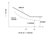
- FIG. 1 is a graph of an S-N curve.
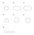
- FIG. 2 is a diagram illustrating an example of a cross-sectional shape of an aluminum wiring material.
- FIG. 1 is a schematic diagram showing a simulated power semiconductor device for evaluation in a resin-encapsulated state for evaluating power cycle life and vibration fatigue.
- 1 is a diagram showing an observation region R of an aluminum wiring material when observing an upper crack. This is a photograph of an aluminum wiring material with a crack occurring on the upper side.
- FIG. 7 is an enlarged photograph of a part of FIG. This is a photograph of an aluminum wiring material with no cracks on the upper side.
- the aluminum wiring material of the embodiment is an aluminum wiring material made of aluminum with a purity of less than 99.9 mass%, and in a cross section perpendicular to the longitudinal direction of the aluminum wiring material, the orientation ratio of the crystal orientation ⁇ 112>, which has an angle difference of 10° or less with respect to the longitudinal direction, is 45% or less.
- the inventors produced multiple wiring material samples using aluminum of different compositions and manufacturing conditions, and evaluated the long-term reliability of the junctions (hereinafter also referred to as "power cycle life") for each sample, as described below, while also carefully observing the cross-sectional structure perpendicular to the longitudinal direction of the wiring material samples.
- power cycle life the long-term reliability of the junctions
- the ratio of crystal orientation ⁇ 111> is widely controlled.
- the ratio of crystal orientation ⁇ 111> it has become possible to put into practical use wire products that are easy to process and soft.
- controlling the ratio of crystal orientation ⁇ 111> alone is not enough to solve the problems of improving the long-term reliability of the joint under temperature cycles, improving the ability to follow the wedge tool, and improving vibration resistance as described above. Therefore, the inventors of the present invention thought that it is important to mix specific orientations that have higher deformation resistance due to the nature of the metal structure than the ⁇ 111> orientation and optimize their ratio in order to solve the problems described above.
- the abundance ratio of the crystal orientation ⁇ 112> which has an angle difference with the longitudinal direction of 10° or less, is 45% or less, thereby achieving an excellent power cycle life and also achieving high vibration resistance, which will be described later.
- the abundance ratio of the crystal orientation ⁇ 112> is preferably 10% or more and 40% or less, and more preferably 15% or more and 35% or less.
- the power cycle test is a test in which a current is passed through the aluminum wiring material so that the surface temperature of the power chip bonded to the aluminum wiring material reaches 150° C., and then the current is stopped and the power chip is cooled down to a surface temperature of 25° C. This test repeats cycles of rapid cooling and rapid heating with a temperature difference of 125° C., and evaluates the number of cycles until a problem occurs in the operation of the power chip. The number of cycles at which current can no longer be passed is determined as the sample life (power cycle life) of the power cycle test. The longer the power cycle life, the better the long-term reliability of the bond.
- the inventors then carefully observed the metal structure of cross sections perpendicular to the longitudinal direction of wiring material samples fabricated in the same manner as above. As a result, they discovered that the precipitated particles on the aluminum-based matrix differ in shape (aspect ratio of the long and short axes when approximated as an ellipse) and in the distribution of the aspect ratios of the precipitated particles, depending on the composition of the wiring material sample and the manufacturing conditions.
- the ratio of the number of precipitate particles having an aspect ratio of 4 or more to the total number of precipitate particles in a cross section perpendicular to the longitudinal direction is 0.5% or more and 16% or less.
- the ratio of the number of precipitate particles having an aspect ratio of 4 or more is preferably 0.7% or more and 12% or less, and more preferably 1% or more and 8% or less.
- the precipitated particles are particles with a size (maximum particle length) of approximately 30 ⁇ m or less, and are shaped like lumps, rings, plates, needles, roughly spherical particles, irregular shapes, etc. These are thought to include particles that crystallize or precipitate during the manufacturing process, as well as particles contained in the aluminum raw materials.
- the precipitated particles are also thought to include any one or more of the following: alloys of aluminum and iron, intermetallic compounds, alloys of aluminum, iron, and silicon, intermetallic compounds, and precipitates of silicon alone.
- the number of precipitated particles and the distribution of the aspect ratios of the precipitated particles can be controlled by the composition of the wiring material (the proportion of iron and silicon), the heat treatment temperature, time, timing of the heat treatment, wire drawing conditions, etc.
- the measurement points it is preferable to ensure the objectivity of the measurement data.
- shorter intervals may be used as long as the objectivity of the measurement data can be ensured.
- the number of precipitated particles and the distribution of the aspect ratios of the precipitated particles can be observed as follows.
- the observation surface of the observation sample is exposed by embedding polishing, and then buffing and milling are performed to remove any irregularities and contamination on the sample surface (to make the surface extremely clean).
- the precipitated particles are identified at 1,000x magnification using an FE-SEM (field emission scanning electron microscope, Hitachi High-Tech SU8220), and then the accelerating voltage is set to 5 kV and the working distance (WD) to 10 mm, and the particles are observed using a backscattered electron image (BED-C).
- the precipitated particles are observed over a wide range of the cross section at 400x magnification, and one to three average locations of the particle distribution are observed at 1,000x magnification. If it is difficult to identify the average location at 1,000x magnification, it is advisable to observe around three locations at 1,000x magnification. In this way, when observing a plurality of locations, the average value of the observed locations should be taken as the aspect ratio value. In addition, if it is desired to observe the entire sample, observation may be performed at 400x magnification, but for samples with fine particles, observation at 1,000x magnification is more preferable than observation at 400x magnification.
- the observer may select the observation magnification appropriately depending on the wire diameter and particle size, but from the viewpoint of measurement accuracy, observation at 1,000x magnification can obtain a more accurate value.
- the observation of precipitated particles is preferably performed at a magnification of 400x or more and 1,000x or less, and within this range, a higher magnification is more preferable.
- the image obtained is adjusted so that the precipitated particles and the aluminum base are clearly visible.
- the composition of the aluminum wiring material differs from that of other areas, so precipitate particles with smaller atomic weight (density) than aluminum, for example, are displayed as pixels with high brightness values.
- areas other than the precipitate particles (in the aluminum matrix) are displayed with low brightness values.
- the brightness values of this FE-SEM image are normalized to a range of 0 to 1 to make it easier to distinguish precipitate particles.
- a luminance value threshold value e.g., 0.95 capable of separating precipitate particles from other regions is determined using a histogram or the like, and binarized to 1 and 0 at the threshold value. As a result, regions with a luminance value of 0 are shown as black, and regions with a luminance value of 1 are shown as white.
- the number of regions (regions with a luminance value of 1) observed as precipitate particles in the processed image binarized to 1 and 0, and the aspect ratio of each region are measured using an image analysis program (e.g., an image analysis program using MATLAB language). From the calculated number of precipitate particles and the aspect ratio (distribution of aspect ratio) of each precipitate particle, the ratio of the number of precipitate particles with an aspect ratio of 4 or more to the total number of precipitate particles is calculated.
- the region observed as precipitate particles is approximated to an ellipse, and the value of the major axis/minor axis of the ellipse is calculated as the aspect ratio of the precipitate particle.
- the elliptical approximation of the precipitate particle can be performed by the least squares method using the center coordinates of the precipitate particle and the coordinates of each point on the periphery of the precipitate particle region. If it is difficult to identify precipitated particles using FE-SEM, the EDX mapping image may be used for binarization, but it is preferable to identify precipitated particles using FE-SEM.
- the fine crystal grains in the crystal structure of the aluminum wiring material of this embodiment increase the elasticity of the crystal structure, which, in combination with the presence rate of the above-mentioned ⁇ 112> orientation ratio, further improves wedge tool followability.
- the average crystal grain size in a cross section perpendicular to the longitudinal direction is preferably 40 ⁇ m or less, in which case wedge tool followability is more easily obtained.
- the average crystal grain size is preferably 30 ⁇ m or less, and more preferably 20 ⁇ m or less.
- the average crystal grain size is usually 1 ⁇ m or more.
- the electron backscatter diffraction pattern (EBSP) method can be used to measure and analyze the cross-sectional crystal structure of aluminum wiring material.
- the EBSP method makes it possible to measure the cross-sectional crystal structure of even thin wires, such as wiring material used in semiconductor bonding, with high precision and sufficient reproducibility.
- the EBSP method can be used to measure and analyze the crystal orientation of the cross section of the wiring material with high precision. By measuring the crystal orientation at at least three different locations, and preferably at least ten different locations, it is possible to obtain an average value that takes variability into account.
- the aluminum wiring material of this embodiment has a load stress ratio defined by the following (1) of 0.4 or more and 0.9 or less.
- Load stress ratio fatigue limit / tensile strength ... (1)
- vibrations caused by a car running or a person walking occur randomly in three directions, X, Y, and Z, and that the vibration frequency is often 40 Hz or less.
- aluminum wiring materials installed in electric vehicles are pulled, compressed, and bent in three directions over a long period of time due to the above-mentioned stresses.
- the inventors have investigated methods for evaluating the performance against such vibration loads with complex directionality. As a result, they have found that the above-mentioned vibration resistance correlates with the load stress ratio shown in the above formula (1).
- the S-N curve shown in Figure 2 is a two-axis graph with the magnitude of this repeated stress on the Y axis and the number of repetitions on the X axis.
- the S-N curve becomes horizontal around 10 to the power of 6 to 10 to the power of 7, and it may not break even if it is subjected to an infinite number of repeated stresses.
- the value of the repeated stress at this time is called the fatigue limit.
- the S-N curve of non-ferrous metals such as aluminum does not become horizontal as shown in Figure 2, and there is no fatigue limit.
- the strength at a certain number of repetitions is considered to be the fatigue limit.
- a repeated stress that does not break up until 10 to the power of 7 is called the 10 to the power of 7 time strength.
- the 10 to the power of 7 time strength is used as the fatigue limit.
- the fatigue limit is usually expressed as the maximum load stress (MPa).
- MPa maximum load stress
- the fatigue limit of the present invention can be measured as follows by performing a tensile fatigue test at room temperature (e.g., 25°C) in accordance with the spirit of JIS Z 2273:1978 using a dedicated tensile fatigue tester (ElectroPlusE3000 manufactured by Instron, hereinafter referred to as the "measurement device"): The aluminum wiring material to be evaluated is cut to a length slightly longer than 100 mm to obtain an evaluation sample with a measurement length of 100 mm. In addition, in order to calculate the value of the maximum load stress described later, the 0.2% proof stress value of the aluminum wiring material to be evaluated is obtained in advance by a tensile test.
- the maximum load stress here is 90% of the 0.2% yield strength and any value less than 90%, and the minimum load stress is 10 MPa (fixed value).
- the 90% value of the 0.2% yield strength is set as the maximum value, and any value less than 90% is set in ascending order, and the above loading and unloading are repeated at three or more different load cycles.
- results are plotted on a semi-logarithmic graph with the x-axis representing the load cycle and the y-axis representing the maximum load stress ⁇ , and the x-axis representing logarithmic (logarithmic base is 10) to create an S-N curve.
- the test conditions are adjusted so that the interval between the load cycles plotted on the graph is 1 or more in the logarithmic display and 10 to the power of 1 in the real display in the x-axis direction.
- An approximate straight line is obtained from the plotted points by the least squares method, and the maximum load stress at which the load cycle does not lead to breakage at 10 to the power of 7 is obtained from the approximate straight line.
- the maximum load stress at which the repeated load count of 107 does not result in fracture is the fatigue limit (MPa).
- MPa the fatigue limit
- the maximum load stress at a repeated load count that does not lead to fracture and is between 103 and 106 may be plotted at three or more points on a semi-logarithmic graph of an S-N curve, an approximation line is found from the plotted points by the least squares method, and the fatigue limit at a repeated load count of 107 may be estimated using the approximation line.
- the test conditions are adjusted so that the interval between the plotted points in the x-axis direction is 1 or more in logarithmic display and 101 or more in real number display.
- the test conditions are adjusted so that the interval between the plotted points in the x-axis direction is 1 or more in logarithmic display and 101 or more in real number display.
- it is important to satisfy the following three conditions. (i) Both ends of the measuring length (the part being pulled) are fixed and do not move during the test. (ii) Both ends of the measuring length are pulled straight toward each other in one axial direction. (iii) The point of fracture during the tensile test is not the chuck part.
- Tensile strength is obtained by dividing the maximum load (kgf) when both ends of an evaluation sample are pulled by a tensile testing device by the cross-sectional area of the wiring material. This maximum load is automatically calculated by converting the tensile force into an electrical signal in the tensile testing device. Note that the load stress ratio is calculated as the value of fatigue limit/tensile strength as shown in the above formula (1), but it may also be calculated as the value of maximum load in tensile fatigue test/maximum load in tensile test.
- the aluminum wiring material of this embodiment has a load stress ratio of 0.4 or more and 0.9 or less, which significantly suppresses damage caused by vibration at the neck portion of the wiring material bonded to the semiconductor chip, thereby improving vibration resistance.
- the load stress ratio is preferably 0.5 or more and 0.9 or less, more preferably 0.6 or more and 0.9 or less, and even more preferably 0.7 or more and 0.9 or less. If the load stress ratio is in this range, the vibration resistance effect can be improved.
- the strength ratio is preferably 1.2 or more and 2.1 or less, and more preferably 1.4 or more and 1.9 or less.
- the yield strength ratio is a value obtained by dividing the maximum stress (MPa) by the 0.2% yield strength (stress) (MPa).
- MPa maximum stress
- 0.2% strain load 0.2% strain load
- the yield strength ratio can be calculated by applying these to the above formula (2). Also, the yield strength ratio may be calculated as the value of the maximum load of the tensile test / 0.2% strain load.
- the wiring material sample is bonded to two aluminum plates at the first and second bonding portions using an ultrasonic bonding device (REBO7 wire bonder manufactured by Ultrasonic Industries) so that the loop height is 1 mm and the length is 7 mm, to obtain an evaluation sample.
- an ultrasonic bonding device REBO7 wire bonder manufactured by Ultrasonic Industries
- a vibration fatigue test is performed using a dedicated vibration fatigue tester manufactured based on JIS standards (e.g., CV-101M manufactured by AS ONE Corporation) to evaluate vibration resistance.
- JIS standards e.g., CV-101M manufactured by AS ONE Corporation
- the aluminum wiring material of this embodiment has excellent vibration resistance due to the above-mentioned configuration, and can suppress failures when exposed to vibration for long periods of time. Furthermore, power semiconductors are subjected to the above-mentioned vibrations under temperature cycles caused by electric currents, but the aluminum wiring material of this embodiment, due to the above-mentioned configuration, is extremely unlikely to break or break even when subjected to a combination of temperature cycles and vibrations. Therefore, a high level of safety can be achieved when used in electric vehicles.
- Ultrasonic bonding a method for bonding aluminum wiring materials, applies ultrasonic waves while applying a load to the aluminum wiring materials, destroying oxide films on the bonding surfaces and deforming the wiring materials while bonding them. Therefore, the thicker the oxide films on the surfaces of the bus bars and electrodes to be bonded, the higher the load and energy of the ultrasonic waves applied to the aluminum wiring materials to remove them.
- the vibrations can cause a decrease in the strength of the wiring materials, especially near the bonding boundary, which can result in a decrease in the long-term reliability of the bond.
- the aluminum wiring materials of this embodiment can achieve excellent vibration resistance and power cycle life as described above, so that even aluminum wiring materials ultrasonically bonded at high loads and high energy can maintain the long-term reliability of the bond.
- the aluminum wiring material of this embodiment has excellent vibration resistance, so it can be joined with a lower loop height, which contributes to the miniaturization of power semiconductors.
- IGBTs, MOSFETs, etc. wiring materials and semiconductor chips are generally sealed with resin.
- the sealing resin is not completely in contact with the wiring material or semiconductor chip, and gaps are generally generated between the resin and the wiring material or semiconductor chip. Due to these gaps, vibration resistance is required even in resin-sealed power semiconductors, just like those not sealed with resin.
- the aluminum wiring material of this embodiment has a long power cycle life and excellent vibration resistance, so that even in resin-sealed power semiconductors, breakage due to temperature cycles and vibration can be suppressed.
- the aluminum constituting the aluminum wiring material of this embodiment contains, relative to its total weight, at least one of the elements iron (Fe) and silicon (Si) in a total amount of 0.01% by weight to 1% by weight, and at least one of the elements gallium (Ga) and vanadium (V) in a total amount of 50 ppm by weight to 800 ppm by weight.
- the aluminum wiring material of this embodiment contains these elements, and the above-mentioned distribution of precipitated particles can be obtained by adjusting the manufacturing conditions. Therefore, the aluminum wiring material of this embodiment can provide excellent vibration resistance and long-term reliability of the joint. Iron, silicon, gallium, and vanadium may be contained in the raw materials of the aluminum wiring material beforehand, or may be added during the manufacturing process of the aluminum wiring material.
- a longer power cycle life can be obtained by having the total amount of at least one of the elements iron and silicon be 0.01 mass% or more. Since a long life is easily achieved, the total amount of iron and silicon is preferably 0.02 mass% or more, more preferably 0.05 mass% or more, even more preferably 0.1 mass% or more, and even more preferably 0.13 mass% or more. In order to achieve a long power cycle life while maintaining conductivity, the total amount of iron and silicon is more preferably 0.9 mass% or less, and even more preferably 0.8 mass% or less.
- the amount of iron is preferably 0.01 mass% or more, more preferably 0.03 mass% or more, even more preferably 0.05 mass% or more, particularly preferably 0.1 mass% or more, and even more particularly preferably 0.13 mass% or more, relative to the total amount of the aluminum alloy.
- the amount of iron is preferably 0.95 mass% or less, more preferably 0.9 mass% or less, relative to the total amount of the wiring material.
- the amount of silicon is preferably 0.01 mass% or more, more preferably 0.05 mass% or more, relative to the total amount of the aluminum alloy.
- the amount of silicon is preferably 0.5 mass% or less, and more preferably 0.4 mass% or less.
- the upper limit of the content of at least one of gallium and vanadium is not particularly limited, but is about 1000 ppm by mass.
- the total amount of gallium and vanadium is preferably 800 ppm by mass or less, which makes it easier to suppress the maximum temperature reached by the aluminum wiring material when current is applied.
- the content of gallium and vanadium may be 100 ppm by mass or more, or 150 ppm by mass or more, relative to the total amount of the wiring material.
- the content of gallium and vanadium may be 700 ppm by mass or less, or 600 ppm by mass or less, relative to the total amount of the wiring material.
- the maximum temperature reached when electricity is applied using aluminum wiring material with a purity of 99.99% by mass is 150°C
- the gallium and vanadium content is 1000 ppm by mass or less
- the maximum temperature reached can be kept below 160°C.
- the temperature rise caused by heat generated when electricity is applied can be kept within about 10°C.
- the aluminum wiring material of this embodiment may contain one or more of the following trace elements in addition to iron, silicon, gallium, and vanadium: magnesium (Mg), copper (Cu), nickel (Ni), zinc (Zn), chromium (Cr), manganese (Mn), titanium (Ti), zirconium (Zr), tungsten (W), and scandium (Sc).
- the aluminum wiring material of this embodiment may contain inevitable impurities other than the above-mentioned trace elements.
- the content of the trace elements is an amount that is 0.1 mass% or less in total with respect to the entire wiring material. In addition, the content of the trace elements is, for example, 0.0001 mass% or more with respect to the total amount of the aluminum alloy.
- trace elements may be contained in advance in the raw material of the aluminum wiring material, may be inevitable impurities in the aluminum raw material, or may be added during the manufacturing process of the aluminum wiring material.
- the above trace elements are preferably 0.005 mass% or more, more preferably 0.01 mass% or more, and even more preferably 0.015 mass% or more.
- the content ratio of elements contained in the aluminum wiring material of this embodiment is generally measured by chemical analysis such as inductively coupled plasma (ICP) optical emission spectroscopy, but is not limited to this. For example, it can also be measured similarly by secondary ion mass spectrometry (SIMS), glow discharge mass spectrometry (GDMS), or energy dispersive X-ray spectroscopy (EDX).
- ICP inductively coupled plasma
- SIMS secondary ion mass spectrometry
- GDMS glow discharge mass spectrometry
- EDX energy dispersive X-ray spectroscopy
- the aluminum wiring material of this embodiment is preferably made of an aluminum alloy with an aluminum purity (amount of aluminum relative to the total amount of the aluminum wiring material) of 99% by mass or more. This provides sufficient electrical conductivity and can achieve even better vibration resistance and long-term reliability of the joint.
- the aluminum purity of the aluminum wiring material is preferably 99.9% by mass or less. By having an aluminum purity of 99.9% by mass or less, sufficient amounts of iron, silicon, gallium, vanadium, and trace elements can be contained, which contributes to improving long-term reliability.
- the purity of the aluminum alloy is more preferably less than 99.9% by mass, and even more preferably 99.8% by mass or less.
- the wire diameter of the aluminum wiring material of this embodiment is usually 15 ⁇ m to 700 ⁇ m, preferably 70 ⁇ m to 600 ⁇ m, and more preferably 100 ⁇ m to 500 ⁇ m.
- the wire diameter of the aluminum wiring material is the diameter if the cross-sectional shape is a perfect circle, and the length of the major axis is the diameter if the cross-sectional shape is other than that (the cross-section is circular, elliptical, oval, polygonal, or polygon-like shape as shown below). However, if the cross-section is polygonal or polygon-like, the length may be measured as the width or thickness.
- Figure 2 shows a schematic example of the cross-sectional shape of the aluminum wiring material.
- the cross-sectional shape of the aluminum wiring material may be a circle (a in Figure 3), an ellipse (e.g., b in Figure 3), an oval (e.g., c in Figure 3), a square (e.g., e in Figure 3), a triangle (e.g., d in Figure 3), or a polygon-like shape (e.g., f and g in Figure 3).
- the length of the long axis is preferably 0.3 mm to 4 mm, more preferably 0.5 mm to 3 mm, and the length of the short axis is preferably 0.05 mm to 0.5 mm, and more preferably 0.1 mm to 0.5 mm.
- the length of the long side is preferably 0.3 mm to 4 mm, more preferably 0.5 mm to 3 mm, and the length of the short side is usually preferably 0.05 mm to 0.5 mm, and more preferably 0.1 mm to 0.5 mm.
- wiring material with a cross section of a polygon, polygon-like, or flat ellipse (a shape obtained by compressing an ellipse in a uniaxial direction) is called a ribbon, and wiring material with a cross section of a circle, ellipse, or ellipse is called a wire.
- the method for manufacturing an aluminum wiring material is not limited to the manufacturing method shown below. It is preferable to adjust the conditions appropriately in consideration of the weight of the aluminum wiring material to be manufactured and the processing capacity of the heat treatment furnace.
- Molten aluminum is prepared by dissolving iron and silicon together in high-purity aluminum of 99% by mass or more.
- the purity of the high-purity aluminum used as a raw material may be 99.9% by mass or more, or may be 99.99% by mass or more.
- a heating furnace such as an arc heating furnace, a high-frequency heating furnace, a resistance heating furnace, or a continuous casting furnace is used.
- the molten aluminum in the heating furnace may be melted while being held in a vacuum or in an inert gas atmosphere such as argon or nitrogen in order to prevent the inclusion of oxygen or hydrogen from the air.
- an inclusion removal process in which an inert gas such as argon (Ar) gas or nitrogen gas is bubbled into the molten aluminum, and then a filtration process is performed using a filter.
- an inert gas such as argon (Ar) gas or nitrogen gas
- a filtration process is performed using a filter.
- inclusions such as silicon dioxide (SiO 2 ) and aluminum oxide (Al 2 O 3 ) are coagulated on the surface of the molten aluminum by bubbling the inert gas, and the inclusions can be removed from the molten aluminum by a subsequent filtration process.
- argon (Ar) gas is used in the inclusion removal process, it becomes easier to adjust the proof stress ratio and the ⁇ 112> orientation ratio to an upper range while increasing the load stress ratio, and it is possible to further improve the long-term reliability and vibration resistance of the joint under temperature cycles.
- the gas flow rate is too high or the bubbling time is too long, once the inclusion removal effect has reached its limit, no further effect is obtained and it is a waste.
- a bubbling method in order to prevent impurities from leaching into the molten aluminum, it is preferable to use a steel pipe, which has excellent corrosion resistance at high temperatures, and bubble an inert gas through the pipe.
- a filtration method there is a method in which the molten aluminum is passed through a ceramic foam filter with a porosity of about 0.8 to 0.9.
- Table 1 shows the difference in the load stress ratio, yield strength ratio, and ⁇ 112> orientation ratio of aluminum wiring material of the final wire diameter when an inclusion removal process was performed (with bubbling) and when it was not performed (without bubbling), with other manufacturing conditions being the same.
- the effects of the presence or absence of bubbling were compared for composition A of 0.15 mass% iron (Fe), 0.03 mass% Si (silicon), 0.009 mass% Ga (gallium), 0.012 mass% vanadium (V), with the remainder being aluminum and unavoidable impurities, and composition B of 0.8 mass% iron (Fe), 0.2 mass% Si (silicon), 0.03 mass% Ga (gallium), 0.03 mass% vanadium (V), with the remainder being aluminum and unavoidable impurities.
- Table 1 when an inclusion removal process is performed on molten aluminum, it is easier to adjust the load stress ratio, yield strength ratio, and ⁇ 112> orientation ratio to the ranges of this embodiment compared to when the process is not performed.
- the melted aluminum material is solidified by continuous casting from a heating furnace to a predetermined diameter to produce an ingot, which can then be set in an extruder and extruded to a predetermined wire diameter.
- it is preferable to perform a scratch prevention treatment process in which the original wire material extruded to a predetermined wire diameter is subjected to a scratch prevention treatment. By undergoing the scratch prevention treatment process, it becomes easier to adjust the yield strength ratio to more than 1.0 and 2.3 or less.
- the scratch prevention treatment can be performed by applying a treatment liquid containing a surfactant as a main component to the surface of the original wire material.
- surfactants contained in the treatment liquid for the scratch prevention treatment process include alcohol-based solvents such as ethanol, methanol, butanol, n-propyl alcohol, phenol, ethylene glycol, tridecanol, and glycerin.
- alcohol-based solvents such as ethanol, methanol, butanol, n-propyl alcohol, phenol, ethylene glycol, tridecanol, and glycerin.
- the concentration of the surfactant used in the scratch prevention treatment process is not particularly limited, but in terms of making it easier to adjust the proof stress ratio to more than 1.0 and not more than 2.3, when a surfactant is used in the subsequent wire drawing process, it is preferable to use the same concentration as the surfactant in the wire drawing process.
- the wire obtained in the above process is drawn into an intermediate wire having a diameter of 5.0 mm, which is usually about 7 to 330 times the final wire diameter.
- the wiring material (intermediate wire material) after the wire drawing process may be subjected to a homogenization treatment (homogenization treatment process).
- the intermediate wire material is subjected to a heat treatment in an atmospheric furnace at 400°C to 500°C for about 30 minutes to 240 minutes, and then quenched.
- the quenching in the homogenization treatment process is not particularly limited, and can be performed by a method of immersing the intermediate wire material after heating in cold water stored in an immersion tank or the like, or a method of pouring cold water over the intermediate wire material after heating with a shower or the like.
- a method of immersing the intermediate wire material after heating in cold water stored in an immersion tank or the like or a method of pouring cold water over the intermediate wire material after heating with a shower or the like.
- a solution treatment may be performed to dissolve elements other than aluminum in the aluminum matrix.
- the intermediate wire after the homogenization treatment may be subjected to an intermediate heat treatment before wire drawing.
- the intermediate heat treatment for example, the intermediate wire after the homogenization treatment is heated at 240 to 300°C for about 30 to 140 minutes, and then air-cooled.
- the intermediate heat treatment can finely adjust the ⁇ 112> orientation ratio, the load stress ratio, and the proof stress ratio.
- the intermediate heat treatment can be performed by passing the intermediate wire through a heating atmosphere heated to a predetermined temperature, or by a batch-type heat treatment in which the wire is heated in a closed furnace.
- the intermediate wire is subjected to homogenization treatment, solution treatment, and intermediate heat treatment as necessary, and then drawn to the final wire diameter.
- the wire is passed through a number of carbide or diamond dies in order to reduce the wire diameter stepwise.
- the reduction in area (processing rate) per die is 5% to 40%.
- the temperature of the wiring material is suppressed from increasing due to friction between the die and the wiring material, and this makes it easier to adjust the ⁇ 112> orientation ratio of the aluminum wiring material to 45% or less, and also makes it possible to obtain a homogeneous ⁇ 112> orientation ratio for the entire aluminum wiring material.
- a die cooling method a method of spraying a cooling liquid containing cold water at the die inlet is effective.
- a lubricant mainly composed of a surfactant may be flowed into the die at the same time as cooling the die, which makes it easier to adjust the load stress ratio to the above range.
- the lubricant can be mixed and supplied into the cooling liquid, so that the lubricant can be efficiently flowed into the die.
- the temperature of the cooling liquid is 20° C. or less and the flow rate of the sprayed cooling liquid is large, the cooling effect is high and the orientation ratio of ⁇ 112> is likely to be homogeneous.
- the flow rate of the cooling liquid is too high, the cooling effect is limited and the liquid is likely to be wasted.
- the wiring material is drawn to the final wire diameter and then subjected to a final heat treatment.
- the final heat treatment mainly removes any distortion in the metal structure remaining inside the wiring material, which allows the mechanical properties of the wiring material to be adjusted.
- the final heat treatment method includes a running heat treatment in which the wiring material is passed through a heated atmosphere heated to a predetermined temperature, and a batch type heat treatment in which the wiring material is heated in a closed furnace.
- the final heat treatment is preferably performed as a batch type heat treatment at 150°C to 400°C for 30 minutes to 60 minutes.
- the higher the final heat treatment temperature and the longer the final heat treatment time the larger the ratio of the number of precipitated particles with an aspect ratio of 4 or more is likely to be, and the lower the final heat treatment temperature and the shorter the final heat treatment time, the smaller the ratio of the number of precipitated particles with an aspect ratio of 4 or more is likely to be.
- the wiring material that has been subjected to the final heat treatment is preferably subsequently air-cooled.
- Air-cooling makes it easier to adjust the ⁇ 112> orientation ratio of the aluminum wiring material uniformly to 45% or less. This is because, although water-cooling has a higher cooling effect than air-cooling, air-cooling does not cause contamination or defects on the surface of the aluminum wiring material, and is easier to uniformly and precisely control the ⁇ 112> orientation ratio to 45% or less while achieving the above-mentioned yield strength ratio and load stress ratio, compared to water-cooling.
- Air-cooling methods include, for example, a method of slowly cooling the aluminum wiring material after the final heat treatment by leaving it at room temperature, and a method of spraying cold air on the surface of the aluminum wiring material.
- the method of spraying air or cold air on the surface of the aluminum wiring material is preferable because it makes it easier to adjust the ⁇ 112> orientation ratio to the desired range uniformly and stably.
- air-cooling is performed by spraying air or cold air on the surface of the aluminum wiring material, the lower the temperature of the air or cold air and the higher the wind speed of the spray, the higher the cooling effect and the easier it is to stably obtain the ⁇ 112> orientation ratio in the above range.
- the manufacturing method for aluminum wiring material of the embodiment described above by adjusting the conditions for the inclusion removal process in the molten metal, the homogenization process in the original wire, the die cooling in the wire drawing process, the final heat treatment, and the air cooling after the final heat treatment using the above-mentioned methods depending on the amount and type of elements other than aluminum in the aluminum wiring material, it is possible to adjust the ⁇ 112> orientation ratio, average crystal grain size, load stress ratio, yield strength ratio, and the ratio of the number of precipitated particles with an aspect ratio of 4 or more within preferred ranges.
- the aluminum wiring material of this embodiment can be used in all applications where wiring materials made of iron-based materials, copper-based materials, and aluminum-based materials have been used in the past.
- the aluminum wiring material of this embodiment can be suitably used as a conductive member for power semiconductors, a conductive member such as an electric wire or cable, a battery member, a winding used in a generator or a motor, etc.
- the conductive member for power semiconductors is a bonding wire or a bonding ribbon for semiconductors, etc.
- the battery member is a mesh or net for a current collector, a bonding wiring material for connecting a bus bar to a battery, etc.
- the aluminum wiring materials of the examples were prepared as follows. High-purity aluminum ingots with a purity of 99.9% by mass or more were prepared, and iron, silicon, gallium, and vanadium were added to the wiring materials of each example so that the composition shown in Table 2 was obtained to prepare aluminum alloys.
- the aluminum alloys of each composition were melted under air. In melting the aluminum alloys, argon (Ar) gas was bubbled into the molten aluminum alloy through a steel pipe, and then the inclusions precipitated on the surface of the molten aluminum alloy were filtered using a ceramic foam filter with a porosity of 0.85.
- the flow rate of the argon (Ar) gas at this time was 7 L/min, and the molten metal flux during filtration was 22 kg/min.
- the surface of the wire obtained by extrusion molding was coated with an aqueous solution of ethanol, which is a surfactant, to perform scratch prevention treatment.
- the wire obtained in this way was drawn to an intermediate wire diameter of 5 mm.
- the intermediate wire in the middle of the wire drawing was subjected to intermediate heat treatment at 240°C to 300°C for about 30 to 140 minutes.
- the intermediate wire after the intermediate heat treatment was cooled in air.
- the intermediate wire before and after the intermediate heat treatment was subjected to wire drawing by cold die drawing. In the wire drawing, the area reduction rate (processing rate) per diamond die was set to 5% to 40%.
- a lubricating liquid containing the same type of surfactant as the above-mentioned surfactant at the same concentration as the treatment liquid during the scratch prevention treatment was poured into the diamond die to cool the diamond die.
- the total processing rate until processing to the final wire diameter was set to 99.36%, and the wire drawing was performed to the final wire diameter (400 ⁇ m).
- the aluminum wiring material processed to the final wire diameter was subjected to a final heat treatment in a batch furnace or salt bath at between 150°C and 400°C for 30 to 60 minutes.
- the air-cooled aluminum wiring material was rewound on a spool by a rewinding machine every 300 m. This resulted in an aluminum wiring material with a circular cross section.
- the aluminum wiring materials of the comparative examples were produced as follows. In the same manner as in the examples, aluminum ingot with a purity of 99.9% by mass or more was prepared, and Fe, Si, Ga, V, etc. were added so as to obtain the composition shown in Table 2.
- the aluminum wiring materials of the comparative examples were produced by changing the manufacturing conditions, such as the heat treatment temperature and time at the intermediate wire diameter and final wire diameter, the processing rate from each wire diameter to the next wire diameter, the cooling rate after the intermediate heat treatment, and the area reduction rate of each die, outside the range of the above examples.
- the crystal orientation of the cross section of the aluminum wiring material in the examples and comparative examples was measured as follows.
- the aluminum wiring material was cut into a length of several centimeters to prepare a number of evaluation samples.
- the evaluation samples were attached straight and flat on a metal (Ag-plated frame) plate, taking care not to stretch or sag.
- the evaluation sample was then placed in a cylindrical mold together with the metal plate so that the metal plate was the bottom of the cylinder, and then an embedding resin was poured into the mold, and then a hardener was added to harden the resin.
- the cylindrical resin containing the hardened evaluation sample was then roughly polished with a polisher so that the vertical cross section (hereinafter also referred to as the transverse cross section) in the longitudinal direction of the wiring material was exposed.
- the cut surface was then finished by final polishing, and the residual strain on the polished surface was then removed by ion milling to obtain a smooth surface.
- the ion milling device was finely adjusted so that the cut surface of the wiring material was perpendicular to the longitudinal direction of the wiring material.
- the cross section of the wiring material of the evaluation sample (i.e., the polished surface of the evaluation sample) was attached to the sample stage of a field emission scanning electron microscope (FE-SEM, JEOL JSM-7800F) so that it was parallel to the sample stage, and the crystal orientation and average crystal grain size of the cross section were measured using the FE-SEM at a magnification of 200x, an acceleration voltage of 15 keV, a measurement area of approximately 420 x 420 ⁇ m, and a measurement interval (Step Size) of 1.2 ⁇ m.
- the crystal orientation thus obtained was analyzed using dedicated software for crystal orientation analysis (OIM analysis, manufactured by TSL, hereafter referred to as the dedicated software).
- the conditions for determining crystal grains in the dedicated software were set, and the crystal orientation ratio of the measured sample, i.e., the proportion of each crystal orientation, was analyzed.
- the conditions for determining crystal grains in the dedicated software can usually be set depending on the purpose of the analysis, but since this has almost no effect on the analysis results of the crystal orientation ratio, in this embodiment and comparative example, they were set to recognize two or more pixels connected with an orientation difference of 10° or less as one crystal grain, and the proportion of crystal grains with the ⁇ 112> orientation was calculated.
- CI value Confidential Index
- IQ value Image Quality
- the SEM photographing conditions were set to an acceleration voltage of 5 kV and a working distance (WD) of 10 mm, and a backscattered electron image (BED-C) was selected.
- BED-C backscattered electron image
- the brightness value of the photographed SEM image was normalized to a range of 0 to 1, and the image was binarized with a threshold value of 0.95, and the area with a brightness value higher than the threshold value was determined to be a precipitated particle.
- adjacent pixels in eight neighborhoods of an area on an image recognized as a particle were determined to be one particle.
- Eight neighborhoods refers to eight directions, up, down, left, right, and a 45° rotation of a specific area recognized as a particle, with the specific area being the center, and an area that is in contact in any of these eight directions is defined as one particle. Note that if only the specific area is recognized as a particle and there is no area that is in contact in any of the eight directions, it is not determined to be a particle.
- the aspect ratio (the ratio of the major axis to the minor axis when the shape of the precipitate particle is approximated as an ellipse circumscribing the precipitate particle (major axis/minor axis)) and the number of precipitate particles in the entire cross section perpendicular to the wire axis direction were measured, and the ratio of the number of precipitate particles with an aspect ratio of 4 or more to the total number of precipitate particles was expressed as a percentage. This ratio was almost the same at the tip, rear end, and middle part of the wire.
- the ratio of the numbers in each example is shown in Table 2.
- the ratio of the total number of precipitate particles to the number of precipitate particles with an aspect ratio of 4 or more in Example 3 and Comparative Example 9 is shown in Table 4.
- the load stress ratio was obtained by the following method. Each aluminum wiring material of the examples and comparative examples was used to obtain an evaluation sample with a measurement length of 100 mm. Using this evaluation sample, a tensile fatigue test was performed using a dedicated testing machine for tensile fatigue tests (ElectroPlusE3000 manufactured by Instron) at room temperature of 15 to 28 ° C. to measure the fatigue limit (MPa).
- Each aluminum wiring material of the examples and comparative examples was cut to a length slightly longer than 100 mm to obtain an evaluation sample separately.
- the tensile strength i.e., the maximum load (Kgf)
- Kgf the maximum load
- the maximum load in the tensile test can be measured using a tensile testing device.
- the maximum load is calculated as the maximum value until the aluminum wiring material of the evaluation sample is broken by continuously pulling it at a speed of 20 mm/min and a load cell rating of 100 N with a measurement length of 100 mm using a tensile testing device (e.g., Shimadzu Corporation Autograph, Model: AGS-5kNX).
- the maximum load is the force applied to the wiring material pulled at the above speed, and is usually calculated automatically by converting the pulling force into an electrical signal using a load cell.
- the maximum load was calculated as the average value of three pieces, taking into account the variation in the measurement results.
- the maximum load was divided by the cross-sectional area of the wiring material to obtain the tensile strength (MPa).
- the yield strength ratio was measured by cutting each of the aluminum wiring materials of the examples and comparative examples to a length slightly longer than 100 mm to obtain an evaluation sample for measuring the yield strength ratio.
- the maximum load (Kgf) and 0.2% strain load (Kgf) of each sample were determined by a tensile test under the same conditions as described above, and each was divided by the cross-sectional area of each sample to calculate the yield strength ratio according to the following formula.
- Yield strength ratio maximum stress / 0.2% yield strength (stress)
- Table 2 The yield strength ratios of the aluminum wiring materials of the Examples and Comparative Examples obtained as described above are shown in Table 2 below.
- the concentration of elements in each aluminum wiring material in the examples and comparative examples was measured as follows. About 0.5 g of the manufactured wiring material was dissolved. The concentration of each element in the solution was determined by high-frequency inductively coupled plasma emission spectroscopy (Shimadzu Corporation, ICPE-9000).
- the elements other than aluminum measured here were iron (Fe), silicon (Si), gallium (Ga), vanadium (V), magnesium (Mg), copper (Cu), nickel (Ni), zinc (Zn), chromium (Cr), manganese (Mn), titanium (Ti), zirconium (Zr), tungsten (W), and scandium (Sc), and the contents of these are shown in Table 2 below. In the table below, the abbreviation "mass" means mass.
- compositions of the aluminum wiring materials of the examples and comparative examples obtained above are shown in Table 2. Next, the following performance evaluations were performed on the aluminum wiring materials obtained above.
- the aluminum wiring materials of the examples and the comparative examples were bonded to the aluminum alloy electrodes of the power chip using an ultrasonic bonding device (REBO7 wire bonder manufactured by Ultrasonic Industries).
- the ultrasonic energy and pressure during bonding were set so that the longitudinal length of the wiring material at the bonding portion was 500 ⁇ m.
- the current, current flow time, and cooling time were set to the power chip so that the maximum temperature (Tjmax) of the power chip was 150° C. and the minimum temperature (Tjmin) was 25° C., that is, the temperature difference between the maximum temperature and the minimum temperature ( ⁇ Tj) was 125° C., and a power cycle test was performed.
- the current flow time was about 7 seconds
- the current stop time was about 13 seconds
- one cycle was about 20 seconds.
- the number of cycles when electricity could no longer be passed was defined as the life in the power cycle test (power cycle life). Samples with a power cycle life of 60,000 cycles or more were judged to be above the target life and were rated as "S” (excellent). A power cycle life of 40,000 to less than 60,000 cycles was judged to be at the target level and were rated as "A” (good). Samples with a power cycle life of 20,000 to less than 40,000 cycles were judged to be a passing grade and were rated as "B" (passable). Samples with a power cycle life of less than 20,000 cycles were rated as "C” (failed). The power cycle test (thermal cycle) evaluations of the aluminum wiring materials in each of the examples and comparative examples are shown in Table 3.
- Each aluminum wiring material of the examples and comparative examples was bonded to two aluminum plates at the first and second joints using an ultrasonic bonding device (REBO7 wire bonder manufactured by Ultrasonic Industries) so that the loop height was 1 mm and the length was 7 mm, and an evaluation sample was obtained.
- the length of the loop is the linear distance between both ends of the first and second joints.
- a vibration fatigue test was performed using a vibration fatigue dedicated tester (CV-101M manufactured by AS ONE Co., Ltd.) manufactured based on the JIS standard, and the vibration resistance was evaluated. In the vibration fatigue test, vibration was applied to each evaluation sample until it broke at a frequency of 50 Hz, an acceleration of 1 G, and an amplitude of 0.099 mm.
- Example 1 and Comparative Example 11 were subjected to corrosion resistance tests in a high humidity environment as follows. Using an ultra-accelerated life test device, the test was performed for up to 1000 hours under conditions of 121°C and 100% RH (saturation). To measure the thickness of the corrosion layer, a cross-section of the wire was prepared using a cross-section milling device, and then the corrosion layer was observed using an FE-SEM. As a result, it was confirmed that the corrosion layer thickness was about 5 ⁇ m in all cases, which was at a level that did not pose any problems when using the wiring materials.
- FIG. 4 shows a schematic diagram of the simulated power semiconductor device 200 for evaluation.
- two stepped aluminum terminals 202 and 203 and an IGBT chip 204 were fixed by die bonding to a metal plate 201 made of tungsten carbide, which was 45 mm long, 40 mm wide, and 2 mm thick.
- a metal spacer was placed on the back surface of one of the aluminum terminals 203 so that it was raised appropriately.
- the IGBT chip 204 and the terminal 203 were bonded by using the aluminum wiring material of the example and the comparative example, and a loop was formed so that the height from the top of the loop to the surface of the terminal 203 was 1 mm, the height from the surface of the IGBT chip 204 to the top of the loop was 10 mm, and the distance between both end faces of the wiring material joint portion, i.e., the length of the wiring material, was 7 mm at the shortest and 20 mm at the longest.
- a wall was formed around the IGBT chip using a commercially available resin dam material, and the inside of the wall, the area surrounding the IGBT chip and the bonding area for the wiring material, was filled with a silicone gel-based sealing resin.
- the number of cycles at which electricity could no longer be passed was defined as the lifespan in this test, and samples with a lifespan of 12 cycles or more were rated "excellent” as they exceeded the target lifespan, samples with 8 to 12 cycles were rated “good” as they met the target level, samples with 4 to 8 cycles were rated “passable” as they passed the test, and samples with less than 4 cycles were rated "fail” as they failed the test.
- Table 5 shows the evaluation of the thermal vibration fatigue test of the aluminum wiring material in each example and comparative example. Comparative examples 9, 10, and 11 were not evaluated because they failed the tool removal evaluation. The results are shown in Table 5. Note that some of the compositions of the wiring material have been omitted in Table 5.
- an aluminum wiring material having the composition shown in Table 7 was prepared in the same manner as in Example 1, and the obtained sample was rolled into a ribbon shape with a long side length of 2 mm and a short side length of 0.2 mm.
- the obtained ribbon-shaped wiring material was used to perform the above-mentioned "thermal vibration fatigue test of resin-encapsulated chip". The results are shown in Table 7.
- the aluminum wiring material of the embodiment was able to simultaneously achieve improved vibration resistance, improved heat resistance, and improved conformability.
- the aluminum wiring material for power semiconductors according to the embodiment can greatly contribute to the development of the power electronics industry, the automobile industry, the electric railway industry, the electric power industry, and the like.
Landscapes
- Chemical & Material Sciences (AREA)
- Engineering & Computer Science (AREA)
- Materials Engineering (AREA)
- Mechanical Engineering (AREA)
- Metallurgy (AREA)
- Organic Chemistry (AREA)
- Physics & Mathematics (AREA)
- Thermal Sciences (AREA)
- Crystallography & Structural Chemistry (AREA)
- Conductive Materials (AREA)
Priority Applications (3)
| Application Number | Priority Date | Filing Date | Title |
|---|---|---|---|
| CN202480050007.6A CN121605207A (zh) | 2023-07-31 | 2024-07-25 | 铝配线材料及其制造方法 |
| JP2025537367A JPWO2025028381A1 (https=) | 2023-07-31 | 2024-07-25 | |
| KR1020267003821A KR20260035248A (ko) | 2023-07-31 | 2024-07-25 | 알루미늄 배선재 및 그 제조방법 |
Applications Claiming Priority (2)
| Application Number | Priority Date | Filing Date | Title |
|---|---|---|---|
| JP2023-124294 | 2023-07-31 | ||
| JP2023124294 | 2023-07-31 |
Publications (1)
| Publication Number | Publication Date |
|---|---|
| WO2025028381A1 true WO2025028381A1 (ja) | 2025-02-06 |
Family
ID=94394593
Family Applications (1)
| Application Number | Title | Priority Date | Filing Date |
|---|---|---|---|
| PCT/JP2024/026568 Pending WO2025028381A1 (ja) | 2023-07-31 | 2024-07-25 | アルミニウム配線材及びその製造方法 |
Country Status (5)
| Country | Link |
|---|---|
| JP (1) | JPWO2025028381A1 (https=) |
| KR (1) | KR20260035248A (https=) |
| CN (1) | CN121605207A (https=) |
| TW (1) | TW202526049A (https=) |
| WO (1) | WO2025028381A1 (https=) |
Citations (8)
| Publication number | Priority date | Publication date | Assignee | Title |
|---|---|---|---|---|
| JPH01255637A (ja) * | 1988-04-05 | 1989-10-12 | Sky Alum Co Ltd | 導電用アルミニウム合金 |
| JP2013258324A (ja) | 2012-06-13 | 2013-12-26 | Tanaka Electronics Ind Co Ltd | 半導体装置接続用アルミニウム合金細線 |
| JP2014129578A (ja) | 2012-12-28 | 2014-07-10 | Tanaka Electronics Ind Co Ltd | パワ−半導体装置用アルミニウム合金細線 |
| WO2019188452A1 (ja) * | 2018-03-27 | 2019-10-03 | 古河電気工業株式会社 | アルミニウム合金材ならびにこれを用いた導電部材、電池用部材、締結部品、バネ用部品および構造用部品 |
| JP2020059886A (ja) | 2018-10-10 | 2020-04-16 | 日鉄マイクロメタル株式会社 | Alボンディングワイヤ |
| WO2020184655A1 (ja) | 2019-03-13 | 2020-09-17 | 日鉄マイクロメタル株式会社 | Alボンディングワイヤ |
| WO2022030620A1 (ja) * | 2020-08-06 | 2022-02-10 | 古河電気工業株式会社 | アルミニウム線材、アルミニウム撚線、被覆電線、圧着端子付き被覆電線、およびcvtケーブルもしくは圧着端子付きcvtケーブル |
| WO2022163606A1 (ja) | 2021-01-28 | 2022-08-04 | 田中電子工業株式会社 | パワー半導体用アルミニウムボンディングワイヤ |
-
2024
- 2024-07-25 JP JP2025537367A patent/JPWO2025028381A1/ja active Pending
- 2024-07-25 WO PCT/JP2024/026568 patent/WO2025028381A1/ja active Pending
- 2024-07-25 CN CN202480050007.6A patent/CN121605207A/zh active Pending
- 2024-07-25 KR KR1020267003821A patent/KR20260035248A/ko active Pending
- 2024-07-31 TW TW113128494A patent/TW202526049A/zh unknown
Patent Citations (8)
| Publication number | Priority date | Publication date | Assignee | Title |
|---|---|---|---|---|
| JPH01255637A (ja) * | 1988-04-05 | 1989-10-12 | Sky Alum Co Ltd | 導電用アルミニウム合金 |
| JP2013258324A (ja) | 2012-06-13 | 2013-12-26 | Tanaka Electronics Ind Co Ltd | 半導体装置接続用アルミニウム合金細線 |
| JP2014129578A (ja) | 2012-12-28 | 2014-07-10 | Tanaka Electronics Ind Co Ltd | パワ−半導体装置用アルミニウム合金細線 |
| WO2019188452A1 (ja) * | 2018-03-27 | 2019-10-03 | 古河電気工業株式会社 | アルミニウム合金材ならびにこれを用いた導電部材、電池用部材、締結部品、バネ用部品および構造用部品 |
| JP2020059886A (ja) | 2018-10-10 | 2020-04-16 | 日鉄マイクロメタル株式会社 | Alボンディングワイヤ |
| WO2020184655A1 (ja) | 2019-03-13 | 2020-09-17 | 日鉄マイクロメタル株式会社 | Alボンディングワイヤ |
| WO2022030620A1 (ja) * | 2020-08-06 | 2022-02-10 | 古河電気工業株式会社 | アルミニウム線材、アルミニウム撚線、被覆電線、圧着端子付き被覆電線、およびcvtケーブルもしくは圧着端子付きcvtケーブル |
| WO2022163606A1 (ja) | 2021-01-28 | 2022-08-04 | 田中電子工業株式会社 | パワー半導体用アルミニウムボンディングワイヤ |
Also Published As
| Publication number | Publication date |
|---|---|
| TW202526049A (zh) | 2025-07-01 |
| KR20260035248A (ko) | 2026-03-12 |
| CN121605207A (zh) | 2026-03-03 |
| JPWO2025028381A1 (https=) | 2025-02-06 |
Similar Documents
| Publication | Publication Date | Title |
|---|---|---|
| KR101474145B1 (ko) | 파워 반도체 장치용 알루미늄 합금 세선 | |
| JP7573051B2 (ja) | パワー半導体用アルミニウムボンディングワイヤ | |
| JP7626905B2 (ja) | Al接続材 | |
| WO2025028381A1 (ja) | アルミニウム配線材及びその製造方法 | |
| WO2025028382A1 (ja) | アルミニウム配線材及びその製造方法 | |
| JP5755892B2 (ja) | 銅合金板の製造方法 | |
| TWI922861B (zh) | Al連接材料 | |
| JP7802189B2 (ja) | 銅ボンディングワイヤ、銅ボンディングワイヤの製造方法及び半導体装置 | |
| TWI922860B (zh) | Al連接材料 | |
| JP7733278B1 (ja) | Alボンディングワイヤ又はAlボンディングリボン | |
| JP7600474B1 (ja) | Al接続材 | |
| TW202548041A (zh) | Al連接材料 | |
| TW202534705A (zh) | 銅接合帶、銅接合帶之製造方法及半導體裝置 |
Legal Events
| Date | Code | Title | Description |
|---|---|---|---|
| 121 | Ep: the epo has been informed by wipo that ep was designated in this application |
Ref document number: 24849036 Country of ref document: EP Kind code of ref document: A1 |
|
| ENP | Entry into the national phase |
Ref document number: 2025537367 Country of ref document: JP Kind code of ref document: A |
|
| WWE | Wipo information: entry into national phase |
Ref document number: 2025537367 Country of ref document: JP |
|
| ENP | Entry into the national phase |
Ref document number: 1020267003821 Country of ref document: KR Free format text: ST27 STATUS EVENT CODE: A-0-1-A10-A15-NAP-PA0105 (AS PROVIDED BY THE NATIONAL OFFICE) |
|
| WWE | Wipo information: entry into national phase |
Ref document number: 1020267003821 Country of ref document: KR |
|
| WWE | Wipo information: entry into national phase |
Ref document number: 202617018335 Country of ref document: IN |
|
| WWE | Wipo information: entry into national phase |
Ref document number: 2024849036 Country of ref document: EP |
|
| NENP | Non-entry into the national phase |
Ref country code: DE |
|
| WWP | Wipo information: published in national office |
Ref document number: 1020267003821 Country of ref document: KR |