WO2025022775A1 - コンデンサモジュール - Google Patents
コンデンサモジュール Download PDFInfo
- Publication number
- WO2025022775A1 WO2025022775A1 PCT/JP2024/018522 JP2024018522W WO2025022775A1 WO 2025022775 A1 WO2025022775 A1 WO 2025022775A1 JP 2024018522 W JP2024018522 W JP 2024018522W WO 2025022775 A1 WO2025022775 A1 WO 2025022775A1
- Authority
- WO
- WIPO (PCT)
- Prior art keywords
- electrode
- bus bar
- extension portion
- capacitor
- insulating
- Prior art date
- Legal status (The legal status is an assumption and is not a legal conclusion. Google has not performed a legal analysis and makes no representation as to the accuracy of the status listed.)
- Pending
Links
Images




Classifications
-
- H—ELECTRICITY
- H01—ELECTRIC ELEMENTS
- H01G—CAPACITORS; CAPACITORS, RECTIFIERS, DETECTORS, SWITCHING DEVICES, LIGHT-SENSITIVE OR TEMPERATURE-SENSITIVE DEVICES OF THE ELECTROLYTIC TYPE
- H01G2/00—Details of capacitors not covered by a single one of groups H01G4/00-H01G11/00
- H01G2/10—Housing; Encapsulation
-
- H—ELECTRICITY
- H01—ELECTRIC ELEMENTS
- H01G—CAPACITORS; CAPACITORS, RECTIFIERS, DETECTORS, SWITCHING DEVICES, LIGHT-SENSITIVE OR TEMPERATURE-SENSITIVE DEVICES OF THE ELECTROLYTIC TYPE
- H01G4/00—Fixed capacitors; Processes of their manufacture
- H01G4/002—Details
- H01G4/228—Terminals
-
- H—ELECTRICITY
- H01—ELECTRIC ELEMENTS
- H01G—CAPACITORS; CAPACITORS, RECTIFIERS, DETECTORS, SWITCHING DEVICES, LIGHT-SENSITIVE OR TEMPERATURE-SENSITIVE DEVICES OF THE ELECTROLYTIC TYPE
- H01G4/00—Fixed capacitors; Processes of their manufacture
- H01G4/40—Structural combinations of fixed capacitors with other electric elements, the structure mainly consisting of a capacitor, e.g. RC combinations
Definitions
- This disclosure relates to a capacitor module.
- a capacitor module is known that has a capacitor element housed in a case and a bus bar connected to the capacitor element.
- Patent Document 1 discloses a film capacitor that includes a capacitor element, a first bus bar, a second bus bar, a case, and a filling resin.
- the film capacitor described in Patent Document 1 has the problem that it is difficult to reduce inductance.
- This disclosure provides a capacitor module that can reduce inductance.
- a capacitor module includes: one or more capacitor elements each having a first electrode, a second electrode, and a side surface connecting the first electrode and the second electrode; A first bus bar electrically connected to the first electrode; A second bus bar electrically connected to the second electrode; an insulating member that insulates the first bus bar from the second bus bar; a case that houses at least the one or more capacitor elements; A sealing resin filled in the case; Equipped with the insulating member has a first insulating portion extending along the side surface in a direction from the second electrode toward the first electrode, and a second insulating portion extending along the second bus bar, the first bus bar has a first contact portion in contact with the first electrode, a first extension portion extending along the side surface, a second extension portion extending along the first insulating portion, and a third extension portion extending along the second insulating portion, the second bus bar has a second contact portion in contact with the second electrode and a fourth extension portion extending along the second insulating portion,
- the first bus bar electrically connected
- FIG. 1 is a cross-sectional view showing a schematic diagram of a capacitor module 100 according to a first embodiment.
- FIG. 2 is a perspective view showing a capacitor element 10 included in the capacitor module 100 of FIG. 1 .
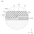
- FIG. 2 is an enlarged view of region R1 in FIG. 1 .
- FIG. 1 is a cross-sectional view illustrating a capacitor module 100A according to a first modified example of the first embodiment.
- FIG. 5 is an enlarged view of region R2 in FIG.
- a first bus bar and a second bus bar each include a first overlapping portion and a second overlapping portion that overlap each other with an insulating plate interposed therebetween.
- the electric field generated by the current flowing through the capacitor element and the electric field generated by the current flowing through the bus bar can be cancelled out, further reducing the inductance of the capacitor module.
- the first bus bar and the second bus bar overlap with an insulating plate interposed between them.
- the insulating plate has a rear plate portion arranged along the side of the capacitor element to ensure a creepage distance between the first bus bar and the second bus bar. Due to the arrangement of the rear plate portion, in the film capacitor of Patent Document 1, it is difficult to make the distance between the side of the capacitor element and the second bus bar smaller than the thickness of the insulating plate. This makes it difficult to further reduce inductance.
- the inventors investigated a capacitor module that allows the busbar to be placed even closer to the side of the capacitor element, and came up with the following invention.
- FIG. 1 is a cross-sectional view showing a capacitor module 100 according to a first embodiment.
- Fig. 2 is a perspective view showing a capacitor element 10 included in the capacitor module 100 of Fig. 1. Note that the X, Y, and Z directions in the figure respectively indicate the horizontal, vertical, and height directions of the capacitor module 100.
- the capacitor module 100 includes a capacitor element 10, a first bus bar 20, a second bus bar 30, an insulating member 40, a case 50, and a sealing resin 60.
- the capacitor module 100 is formed by housing the capacitor element 10, a portion of the first bus bar 20 and the second bus bar 30, and a portion of the insulating member 40 in the case 50, and sealing the case 50 with the sealing resin 60 filled in the case 50.
- Capacitor element 10 is a film capacitor composed of a laminate of dielectric films. More specifically, capacitor element 10 is formed by stacking dielectric films having metal deposition films formed on their surfaces, and then rolling or laminating them. In this embodiment, the roll of dielectric films is pressed into a flat shape, so that capacitor element 10 is formed into a columnar shape having an oval cross section.
- the dielectric film for example, a dielectric film formed from a mixed resin solution containing phenoxy resin and MDI (diphenylmethane diisocyanate) can be used.
- a dielectric film formed from a mixed resin solution containing polyvinyl acetoacetal (PVAA) and tolylene diisocyanate (TDI) can be used.
- PVAA polyvinyl acetoacetal
- TDI tolylene diisocyanate
- the glass transition point of the dielectric film can be made 120°C or higher, and the heat resistance temperature of the capacitor element 10 can be made 120°C or higher. This makes it possible to improve the heat resistance of the capacitor module.
- the metal vapor deposition film formed on the surface of the dielectric film for example, metals such as Al and Zn can be used.
- a first electrode 11 and a second electrode 12 for electrically connecting the bus bar 20 are formed on both ends of the dielectric film laminate of the capacitor element 10.
- the first electrode 11 and the second electrode 12 can be formed by spraying a metal (conductive material) such as Al or Zn.
- the capacitor element 10 has a side surface 13 that connects the first electrode 11 and the second electrode 12.
- the capacitor element 10 is formed in a columnar shape having an oval cross section, so that the side surface 13 of the capacitor element 10 includes a pair of flat portions 13a and a pair of curved portions 13b that connect the pair of flat portions 13a.
- the case 50 is a case for housing the capacitor element 10.
- the case 50 has, for example, a substantially rectangular parallelepiped shape and has an opening 51 through which a portion of the bus bar 20 is exposed.
- the capacitor element 10 is housed in the case 50.
- the capacitor element 10 is disposed inside the case 50 such that the electrodes 11, 12 face a side wall 52 of the case 50 and the flat portion 13a of the side surface 13 faces a bottom wall 53 and the opening 51 of the case.
- portions of the first bus bar 20 and the second bus bar 30 and a portion of the insulating member 40 are housed in the case 50.
- the case 50 is formed from a synthetic resin such as polyphenylene sulfide (PPS resin) or polybutylene terephthalate (PBT resin).
- a synthetic resin such as polyphenylene sulfide (PPS resin) or polybutylene terephthalate (PBT resin).
- sealing resin 60 is filled into case 50 to seal capacitor element 10 housed in case 50, parts of first bus bar 20 and second bus bar 30, and part of insulating member 40.
- Sealing resin 60 is made of a thermosetting resin such as epoxy resin or urethane resin. A material with high fluidity and adhesiveness may be used as the material for sealing resin 60.
- the first bus bar 20 is electrically connected to the first electrodes 11 of the capacitor elements 10, and functions as an external terminal of the capacitor module 100.
- the second bus bar 30 is electrically connected to the second electrodes 12 of the capacitor elements 10, and functions as an external terminal of the capacitor module 100.
- the first bus bar 20 and the second bus bar 30 can be formed, for example, from a conductive metal plate.
- the first busbar 20 has a first contact portion 21, a first extension portion 22, a second extension portion 23, and a third extension portion 24.
- the first contact portion 21 is a portion that contacts the first electrode 11 of the capacitor element 10.
- the first extension portion 22 is arranged to extend from the end portion 21a of the first contact portion 21 along the flat portion 13a of the side surface 13 of the capacitor element 10.
- the second extension portion 23 is arranged to extend along the first insulating portion 41 of the insulating member 40 described later.
- the third extension portion 24 is arranged to extend from the end portion 23a of the second extension portion 23 along the second insulating portion 42 of the insulating member 40 described later.
- the first extension portion 22 and the second extension portion 23 are arranged at different positions in the height direction. More specifically, the first extension portion 22 is arranged at a position closer to the side surface 13 of the capacitor element 10 than the second extension portion 23.
- the second busbar 30 has a second contact portion 31 and a fourth extension portion 32.
- the second contact portion 31 is a portion that contacts the second electrode 12 of the capacitor element 10.
- the fourth extension portion 32 is arranged to extend along the second insulating portion 42 of the insulating member 40.
- the third extension portion 24 of the first busbar 20 and the fourth extension portion 32 of the second busbar 30 are arranged to overlap in the horizontal direction (X direction) of the capacitor module 100 via the insulating member 40. Since the first busbar 20 and the second busbar 30 have overlapping portions, the electric field generated by the current flowing through the third extension portion 24 of the first busbar 20 and the electric field generated by the current flowing through the fourth extension portion 32 of the second busbar 30 cancel each other out, thereby reducing the inductance of the capacitor module 100.
- the insulating member 40 is a member that electrically insulates the first bus bar 20 and the second bus bar 30.
- the insulating member 40 is, for example, a plate-shaped member (insulating plate) formed of a non-conductive material such as resin.
- a high-grade resin that can withstand high voltage for example, PPS (polyphenylene sulfide) material, can be adopted.
- the insulating member 40 has a thickness of, for example, 0.8 mm or more and 1.6 mm or less. By the insulating member 40 having a thickness of 0.8 mm or more and 1.6 mm or less, it is possible to ensure a creepage distance between the first bus bar 20 and the second bus bar 30, or between the first bus bar 20 and the second electrode 12.
- the insulating member 40 has a first insulating portion 41 that extends along the flat portion 13a of the side surface 13 of the capacitor element 10 in the direction from the second electrode 12 to the first electrode 11 of the capacitor element 10 (X direction), and a second insulating portion 42 that extends along the second bus bar 30. As shown in FIG. 1, in this embodiment, the insulating member 40 is bent in an L-shape when viewed from the vertical direction (Y direction) of the capacitor module 100.
- the first insulating portion 41 insulates the first busbar 20 from the second electrode 12.
- the first insulating portion 41 is arranged to extend along the side surface 13, thereby more reliably insulating the first busbar 20 from the second electrode 12.
- the first insulating portion may be arranged to at least partially overlap the second electrode 12 of the capacitor element 10 when viewed from the height direction (Z direction). By arranging the first insulating portion 41 in this manner, it is possible to more reliably insulate the first busbar 20 from the second electrode 12.
- the second insulating portion 42 insulates the first busbar 20 from the second busbar 30, particularly the third extension portion 24 of the first busbar 20 from the fourth extension portion 32 of the second busbar 30.
- FIG. 3 is an enlarged view of region R1 in FIG. 1. The arrangement of the first bus bar 20 and the insulating member 40 will be described with reference to FIG. 3.
- the first extension portion 22 of the first busbar 20 is arranged along the flat portion 13a of the side surface 13 of the capacitor element 10.
- the second extension portion 23 of the first busbar 20 is arranged along the first insulating portion 41 of the insulating member 40. Due to the thickness of the first insulating portion 41, the first extension portion 22 and the second extension portion 23 are arranged at different positions in the height direction (Z direction).
- the first busbar 20 has a connection portion 25 that connects the first extension portion 22 and the second extension portion 23.
- the connection portion 25 is arranged to extend in a direction intersecting the side surface 13 of the capacitor element 10.
- connection portion 25 is arranged to extend approximately perpendicular to the side surface of the capacitor element 10 and is arranged along the end face 41a of the first insulating portion 41. Therefore, the first bus bar 20 is formed in a shape having a step S1 from the first extension portion 22 through the connection portion 25 toward the second extension portion 23. By forming the first bus bar 20 in a shape having a step, the first extension portion 22 and the side surface 13 of the capacitor element 10 can be brought close to each other.
- connection portion 25 is illustrated as extending in a straight line, but the connection portion 25 may be partially or entirely curved due to the convenience of the processing for bending the first bus bar 20, which is a metal plate. Due to the curvature of the connection portion 25, the connection portion 25 may have a portion separated from the first insulating portion 41.
- the first extension 22 is arranged so as to contact the flat portion 13a of the side surface 13 of the capacitor element 10. The closer the distance between the first extension 22 and the capacitor element 10, the greater the effect of reducing inductance.
- the capacitor module 100 includes a capacitor element 10, a first bus bar 20, a second bus bar 30, an insulating member 40, a case 50, and a sealing resin 60.
- the capacitor element 10 has a first electrode 11, a second electrode 12, and a side surface 13 connecting the first electrode 11 and the second electrode 12.
- the first bus bar 20 is electrically connected to the first electrode 11.
- the second bus bar 30 is electrically connected to the second electrode 12.
- the insulating member 40 insulates the first bus bar 20 and the second bus bar 30.
- the case 50 houses at least the capacitor element 10.
- the sealing resin 60 is filled into the case 50.
- the insulating member 40 has a first insulating portion 41 and a second insulating portion 42.
- the first insulating portion 41 extends along the side surface 13 in a direction from the second electrode 12 toward the first electrode 11.
- the second insulating portion 42 extends along the second busbar 30.
- the first busbar 20 has a first contact portion 21, a first extension portion 22, a second extension portion 23, and a third extension portion 24.
- the first contact portion 21 contacts the first electrode 11.
- the first extension portion 22 extends along the side surface 13.
- the second extension portion 23 extends along the first insulating portion 41.
- the third extension portion 24 extends along the second insulating portion 42.
- the second busbar 30 has a second contact portion 31 and a fourth extension portion 32.
- the second contact portion 31 contacts the second electrode 12.
- the fourth extension portion 32 extends along the second insulating portion 42.
- the first extension portion 22 is disposed closer to the side surface 13 than the second extension portion 23.
- This configuration makes it possible to provide a capacitor module that can reduce inductance. Since the first extension portion 22 of the first busbar 20 can be brought close to the side surface 13 of the capacitor element 10, the electric fields between the first busbar 20 and the capacitor element 10 are cancelled out, thereby reducing the inductance of the capacitor module 100.
- the first busbar 20 has a connection portion 25 that extends in a direction intersecting the side surface 13 to connect the first extension portion 22 and the second extension portion 23.
- This configuration allows the first extension portion 22 and the second extension portion 23 to be arranged with a step, and allows the first extension portion 22 to be closer to the side surface 13 of the capacitor element 10. This further reduces the inductance of the capacitor module 100.
- the first extension portion 22 is in contact with the side surface 13.
- the first extension portion 22 of the first bus bar 20 comes into contact with the side surface 13 of the capacitor element 10, thereby further reducing the inductance of the capacitor module 100.
- the first insulating portion 41 at least partially overlaps the second electrode 12.
- This configuration ensures more reliable insulation between the first bus bar 20 and the second electrode 12.
- the heat resistance temperature of the capacitor element 10 is 120°C or higher.
- This configuration makes it possible to suppress damage to the capacitor element 10 due to heat even if heat is transferred from the first bus bar 20 and the second bus bar 30 to the capacitor element 10. This makes it possible to provide a highly heat-resistant capacitor module 100.
- the insulating member 40 is made of a plate-shaped resin.
- This configuration makes it possible to provide a capacitor module 100 that can withstand high voltages.
- connection portion 25 is disposed along the end surface 41a of the first insulating portion 41, but the present invention is not limited to this.
- FIG. 4 is a cross-sectional view showing a capacitor module 100A according to a first variation of the first embodiment.
- FIG. 5 is an enlarged view of region R2 in FIG. 4.
- the shape of the first bus bar 120 differs from that of the capacitor module 100 according to the first embodiment.
- connection portion 125 that connects the first extension portion 122 and the second extension portion 123 of the first bus bar 120 is arranged so as to be inclined with respect to the flat portion 13a of the side surface 13 of the capacitor element 10. With this configuration, the first extension portion 22 and the side surface 13 of the capacitor element 10 can be brought closer together and easily contacted.
- the capacitor module 100 includes one capacitor element 10 has been described, but this is not limiting.
- the capacitor module 100 may include multiple capacitor elements 10.
- the second bus bar 30 is a flat plate, but this is not limiting.
- the second bus bar 30 may have a curved shape similar to the first bus bar 20.
- a capacitor module includes one or more capacitor elements each having a first electrode, a second electrode, and a side surface connecting the first electrode and the second electrode, a first bus bar electrically connected to the first electrode, a second bus bar electrically connected to the second electrode, an insulating member that insulates the first bus bar from the second bus bar, a case that houses at least one or more capacitor elements, and a sealing resin that fills the case, wherein the insulating member extends from the second electrode to the first electrode.
- the first busbar has a first contact portion in contact with the first electrode, a first extension portion extending along the side surface, a second extension portion extending along the first insulating portion, and a third extension portion extending along the second insulating portion
- the second busbar has a second contact portion in contact with the second electrode and a fourth extension portion extending along the second insulating portion, and the first extension portion is positioned closer to the side surface than the second extension portion.
- the first bus bar may have a connection portion extending in a direction intersecting the side surface to connect the first extension portion and the second extension portion.
- the first extension portion may be in contact with the side surface.
- the first insulating portion may at least partially overlap the second electrode.
- the heat resistance temperature of the capacitor element may be 120°C or higher.
- the insulating member may be formed from a plate-shaped resin.
- This disclosure is useful for capacitor modules used in various electronic devices, electrical devices, industrial equipment, vehicle devices, etc.
Landscapes
- Engineering & Computer Science (AREA)
- Power Engineering (AREA)
- Microelectronics & Electronic Packaging (AREA)
- Manufacturing & Machinery (AREA)
- Fixed Capacitors And Capacitor Manufacturing Machines (AREA)
Priority Applications (1)
| Application Number | Priority Date | Filing Date | Title |
|---|---|---|---|
| JP2025535588A JPWO2025022775A1 (https=) | 2023-07-25 | 2024-05-20 |
Applications Claiming Priority (2)
| Application Number | Priority Date | Filing Date | Title |
|---|---|---|---|
| JP2023120590 | 2023-07-25 | ||
| JP2023-120590 | 2023-07-25 |
Publications (1)
| Publication Number | Publication Date |
|---|---|
| WO2025022775A1 true WO2025022775A1 (ja) | 2025-01-30 |
Family
ID=94374754
Family Applications (1)
| Application Number | Title | Priority Date | Filing Date |
|---|---|---|---|
| PCT/JP2024/018522 Pending WO2025022775A1 (ja) | 2023-07-25 | 2024-05-20 | コンデンサモジュール |
Country Status (2)
| Country | Link |
|---|---|
| JP (1) | JPWO2025022775A1 (https=) |
| WO (1) | WO2025022775A1 (https=) |
Citations (5)
| Publication number | Priority date | Publication date | Assignee | Title |
|---|---|---|---|---|
| JP2015095627A (ja) * | 2013-11-14 | 2015-05-18 | ニチコン株式会社 | ケースモールド型コンデンサおよびその製造方法 |
| JP2020182004A (ja) * | 2020-08-03 | 2020-11-05 | パナソニックIpマネジメント株式会社 | コンデンサ |
| JP2020202304A (ja) * | 2019-06-11 | 2020-12-17 | ニチコン株式会社 | ケースモールド型コンデンサ |
| JP2021153120A (ja) * | 2020-03-24 | 2021-09-30 | ニチコン株式会社 | コンデンサのバスバー構造 |
| JP2023008579A (ja) * | 2021-07-06 | 2023-01-19 | 株式会社指月電機製作所 | コンデンサ |
-
2024
- 2024-05-20 JP JP2025535588A patent/JPWO2025022775A1/ja active Pending
- 2024-05-20 WO PCT/JP2024/018522 patent/WO2025022775A1/ja active Pending
Patent Citations (5)
| Publication number | Priority date | Publication date | Assignee | Title |
|---|---|---|---|---|
| JP2015095627A (ja) * | 2013-11-14 | 2015-05-18 | ニチコン株式会社 | ケースモールド型コンデンサおよびその製造方法 |
| JP2020202304A (ja) * | 2019-06-11 | 2020-12-17 | ニチコン株式会社 | ケースモールド型コンデンサ |
| JP2021153120A (ja) * | 2020-03-24 | 2021-09-30 | ニチコン株式会社 | コンデンサのバスバー構造 |
| JP2020182004A (ja) * | 2020-08-03 | 2020-11-05 | パナソニックIpマネジメント株式会社 | コンデンサ |
| JP2023008579A (ja) * | 2021-07-06 | 2023-01-19 | 株式会社指月電機製作所 | コンデンサ |
Also Published As
| Publication number | Publication date |
|---|---|
| JPWO2025022775A1 (https=) | 2025-01-30 |
Similar Documents
| Publication | Publication Date | Title |
|---|---|---|
| JP5391797B2 (ja) | ケースモールド型コンデンサ | |
| CN107710448B (zh) | 电池组 | |
| US10811189B2 (en) | Film capacitor including bus bars having overlapping portions with an insulating part disposed therebetween | |
| US12381337B2 (en) | Busbar connector | |
| US12387881B2 (en) | Capacitor module having a metal sheet between adjacent capacitors | |
| CN109037506B (zh) | 电池组 | |
| JP6305731B2 (ja) | ケースモールド型コンデンサおよびその製造方法 | |
| JPWO2018198527A1 (ja) | コンデンサ | |
| US10984952B2 (en) | Capacitor | |
| KR20150016699A (ko) | 탄탈륨 캐패시터 및 그 제조 방법 | |
| US8906524B2 (en) | Secondary battery having a modular frame to support a protection circuit module | |
| KR20100132467A (ko) | 전력 반도체 모듈의 제조방법, 및 접속장치를 포함하는 전력 반도체 모듈 | |
| WO2025022775A1 (ja) | コンデンサモジュール | |
| KR20160054811A (ko) | 탄탈륨 캐패시터 및 그 제조 방법 | |
| KR20110030762A (ko) | 커패시터용 부스바 조립방법 및 그 제품 | |
| KR102827885B1 (ko) | 복합 콘덴서 | |
| US20200135399A1 (en) | Capacitor | |
| WO2025022776A1 (ja) | コンデンサモジュール | |
| WO2024005012A1 (ja) | コンデンサモジュール | |
| JP2024056186A (ja) | コンデンサ | |
| JP2024080235A (ja) | 収納ケース付きフィルムコンデンサ | |
| JP2012043578A (ja) | 電池 | |
| WO2026058674A1 (ja) | コンデンサモジュール | |
| JP2008147541A (ja) | コンデンサ | |
| WO2026063027A1 (ja) | コンデンサモジュール |
Legal Events
| Date | Code | Title | Description |
|---|---|---|---|
| 121 | Ep: the epo has been informed by wipo that ep was designated in this application |
Ref document number: 24845159 Country of ref document: EP Kind code of ref document: A1 |
|
| ENP | Entry into the national phase |
Ref document number: 2025535588 Country of ref document: JP Kind code of ref document: A |
|
| WWE | Wipo information: entry into national phase |
Ref document number: 2025535588 Country of ref document: JP |
|
| NENP | Non-entry into the national phase |
Ref country code: DE |