WO2025018148A1 - 積層体の製造方法 - Google Patents
積層体の製造方法 Download PDFInfo
- Publication number
- WO2025018148A1 WO2025018148A1 PCT/JP2024/024049 JP2024024049W WO2025018148A1 WO 2025018148 A1 WO2025018148 A1 WO 2025018148A1 JP 2024024049 W JP2024024049 W JP 2024024049W WO 2025018148 A1 WO2025018148 A1 WO 2025018148A1
- Authority
- WO
- WIPO (PCT)
- Prior art keywords
- workpiece
- substrate
- manufacturing
- layer
- laminate according
- Prior art date
- Legal status (The legal status is an assumption and is not a legal conclusion. Google has not performed a legal analysis and makes no representation as to the accuracy of the status listed.)
- Pending
Links
Images


Classifications
-
- G—PHYSICS
- G02—OPTICS
- G02B—OPTICAL ELEMENTS, SYSTEMS OR APPARATUS
- G02B6/00—Light guides; Structural details of arrangements comprising light guides and other optical elements, e.g. couplings
- G02B6/10—Light guides; Structural details of arrangements comprising light guides and other optical elements, e.g. couplings of the optical waveguide type
- G02B6/12—Light guides; Structural details of arrangements comprising light guides and other optical elements, e.g. couplings of the optical waveguide type of the integrated circuit kind
- G02B6/13—Integrated optical circuits characterised by the manufacturing method
- G02B6/138—Integrated optical circuits characterised by the manufacturing method by using polymerisation
Definitions
- the present invention relates to a method for manufacturing a laminate.
- optical/electrical composite substrate is one in which an optical waveguide is provided on a substrate.
- Techniques relating to the optical/electrical composite substrate include those described in, for example, Patent Documents 1 and 2.
- Patent Document 1 describes an opto-electrical hybrid board comprising a flexible circuit board in which electrical wiring having mounting pads is formed on the surface of an insulating layer, an element mounted on the mounting pad, and an optical waveguide laminated on the back surface side of the insulating layer, wherein the flexible circuit board is a flexible double-sided circuit board in which electrical wiring is also formed on the back surface of the insulating layer, and a metallic reinforcing layer is plated on at least the portion of the electrical wiring on the back surface side that corresponds to the mounting pad, and the optical waveguide is in contact with the metallic reinforcing layer.
- a metallic reinforcing layer is adhered to an insulating layer of a flexible circuit board without an adhesive layer, and it is described that an optical-electrical hybrid board can be provided in which elements are properly mounted while suppressing deformation due to a pressure load when the elements are mounted by the metallic reinforcing layer.
- Patent Document 1 describes a method of preparing a substrate having an insulating layer 1 made of a resin such as polyimide and copper foil 21 formed on both sides thereof, and forming through holes 1a and via holes 1b for an optical path in the substrate (see paragraph 0023 of Patent Document 1).
- Patent Document 1 also describes a flexible double-sided circuit board E on which a metallic reinforcing layer M is formed (see paragraph 0028 of Patent Document 1).
- the flexible double-sided circuit board E includes the substrate.
- Patent Document 1 describes that an undercladding layer 6 is formed on the back side of a flexible double-sided circuit board E in contact with a metal reinforcing layer M that covers the electrical wiring 2B on the back side, and describes that examples of a molding material for the undercladding layer 6 include a photosensitive resin and a thermosetting resin (see paragraph 0029 of Patent Document 1). According to Figures 4 to 6 of Patent Document 1, it can be seen that the molding material for the undercladding layer 6 is filled into a recess formed in the flexible double-sided circuit board E on which the metal reinforcing layer M is formed.
- Patent Document 2 describes an optoelectronic wiring board that is formed by integrating a rigid section in which conductor circuits and insulating layers are laminated on both sides of a substrate with one or more bendable flex sections, wherein the rigid section is formed with external connection terminals for mounting optical elements and/or package substrates on which optical elements are mounted, and at least one of the flex sections is formed with optical wiring. It is stated that the optoelectronic wiring board in Patent Document 2 can suitably process large amounts of information and high speed information processing without increasing the size of the wiring board.
- Patent Document 2 describes that the rigid section has an optical signal transmitting region formed therein, and that the optical signal transmitting region is filled with a resin composition (see claims 4 and 5 of Patent Document 2). It also describes that the optical signal transmitting region is formed so as to penetrate all of the substrates and insulating layers that make up the rigid section (see claim 6 of Patent Document 2).
- Patent Document 2 describes a substrate 221 consisting of an optical waveguide film 250 and a surrounding resin layer (insulating layer) 221a, and describes that the resin layer 221a constitutes part of the optical signal transmitting regions 242a, 242b (see paragraph 0033 of Patent Document 2).
- An example of an optoelectronic composite substrate is one that has a laminate including a substrate having a through hole and a first clad layer of an optical waveguide, and the through hole formed in the substrate is filled with a resin composition for forming the first clad layer. According to the studies of the present inventors, it has been found that in such an optoelectronic composite substrate, depressions may occur at the top and/or bottom of the resin composition filled in the through hole.
- the present invention has been developed in consideration of the above circumstances, and aims to provide a method for manufacturing a laminate that can reduce the amount of recession.
- the present invention provides the following method for producing a laminate.
- a method for manufacturing a laminate including a substrate having a through hole and a first clad layer of an optical waveguide comprising the steps of: A step (A) of preparing a workpiece in which the substrate and a layer made of a resin composition for forming the first clad layer are laminated; A method for manufacturing a laminate, comprising: a step (B) of exposing both sides of the workpiece to light.
- a step (B) of exposing both sides of the workpiece to light comprising: a step (B) of exposing both sides of the workpiece to light.
- the step (B) includes a step (B-1) of exposing one surface of the workpiece to light;
- [5] The method for producing a laminate described in [4], wherein in the step (C), the temperature to which the workpiece is heated is 80° C. or higher and 200° C. or lower.
- the workpiece further includes a base film, The method for producing a laminate according to any one of the above [1] to [6], wherein the substrate, a layer made of a resin composition for forming the first clad layer, and the base film are laminated in this order.
- the base film is a resin film, The method for producing a laminate according to [7] above, wherein the resin constituting the resin film includes at least one selected from the group consisting of polyethylene terephthalate, polybutylene terephthalate, and polyethylene naphthalate.
- the present invention provides a method for manufacturing a laminate that can reduce the amount of recession.
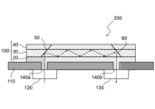
- FIG. 1 is a cross-sectional view showing a schematic example of a structure of an optical/electrical composite substrate according to an embodiment of the present invention.
- FIG. 13 is a diagram for explaining the amount of depression.
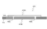
- FIG. 2 is a cross-sectional view showing a schematic example of a structure of a workpiece.
- 1 is a cross-sectional view showing a schematic example of a structure of a workpiece further including a base film.
- FIG. 1 is a cross-sectional view showing a schematic example of the structure of an optical/electrical composite substrate according to this embodiment.
- the optical/electrical composite substrate 200 has an optical waveguide 100 provided on a substrate 110.
- the optical waveguide 100 has a first clad layer 20, a core layer 30, and a second clad layer 40 laminated in this order.
- a mirror 50 on the light-emitting element side and a mirror 60 on the light-receiving element side are formed in the optical waveguide 100.
- the substrate 110 has through holes 140 (140a, 140b) (note that the through holes 140 shown in Fig. 1 are filled with the first clad layer 20).
- a light-emitting element 120 and a light-receiving element 130 are provided on the side of the substrate 110 opposite to the optical waveguide 100 side.
- the light propagation path in the photoelectric composite substrate 200 will be specifically described using Figure 1.
- the light emitted from the light-emitting portion of the light-emitting element 120 passes through the through-hole 140a formed in the substrate 110, enters the mirror 50 on the light-emitting element side, and is transmitted through the core layer 30. After that, it enters the mirror 60 on the light-receiving element side, passes through the through-hole 140b formed in the substrate 110, and enters the light-receiving element 130.
- the arrows in Figure 1 are a schematic representation of the propagation of light.
- a heating process or the like may be performed after filling the through-hole 140 with a resin composition for forming the first cladding layer 20, resulting in depressions on the upper and/or lower sides of the resin composition filled in the through-hole 140.
- FIG. 2 is a diagram for explaining the amount of recess.
- the amount of recess on the upper side refers to the depth of the recess when the surface of the first cladding layer 20 opposite the substrate 110 side is used as a reference.
- the amount of recess on the upper side refers to the depth shown as 10a in FIG. 2.
- the amount of recess on the lower side refers to the depth of the recess when the surface of the substrate 110 opposite the first cladding layer 20 side is used as a reference.
- the amount of recess on the lower side refers to the depth shown as 10b in FIG. 2.
- the present invention has been made in consideration of the above circumstances, and provides a method for producing a laminate that can suppress the amount of recession.
- the method for manufacturing a laminate of this embodiment is a method for manufacturing a laminate comprising a substrate having a through hole and a first clad layer of an optical waveguide, and comprises a step (A) of preparing a workpiece in which the substrate and a layer made of a resin composition for forming the first clad layer are laminated, and a step (B) of exposing both sides of the workpiece to light.
- the "layer made of a resin composition for forming a first cladding layer” may be referred to as the "resin layer (a)".
- the method for producing a laminate of this embodiment includes a step (A) of preparing a workpiece in which a substrate and a layer made of a resin composition for forming a first cladding layer are laminated.
- FIG. 3 is a cross-sectional view showing a schematic example of the structure of a workpiece.
- the workpiece 410 is formed by laminating a substrate 110 and a layer (resin layer (a)) 310 made of a resin composition for forming a first clad layer.
- the substrate 110 has a through hole 140.
- the substrate 110 is not particularly limited as long as it is a substrate having a through hole.
- Examples of the substrate 110 include a printed circuit board and a flexible substrate, and the like.
- a flexible substrate is preferable, and a flexible double-sided copper-clad laminate is more preferable.
- the substrate 110 is preferably a substrate for mounting an optical waveguide.
- the thickness of the substrate 110 is preferably 10 ⁇ m or more, more preferably 30 ⁇ m or more, even more preferably 40 ⁇ m or more, and even more preferably 45 ⁇ m or more, and from the viewpoint of miniaturizing the optoelectronic composite substrate, it is preferably 1000 ⁇ m or less, more preferably 800 ⁇ m or less, even more preferably 500 ⁇ m or less, even more preferably 300 ⁇ m or less, even more preferably 200 ⁇ m or less, even more preferably 100 ⁇ m or less, and even more preferably 80 ⁇ m or less.
- the substrate 110 has at least one through-hole 140 , and may have one through-hole 140 or may have two or more through-holes 140 . 3, the substrate 110 has a through hole 140a on the light emitting element side and a through hole 140b on the light receiving element side. In such a substrate 110, the through hole 140 can be a light propagation path.
- the hole diameter of the through hole 140 is preferably 10 ⁇ m or more, more preferably 30 ⁇ m or more, even more preferably 50 ⁇ m or more, even more preferably 70 ⁇ m or more, even more preferably 90 ⁇ m or more, and preferably 1000 ⁇ m or less, more preferably 800 ⁇ m or less, even more preferably 500 ⁇ m or less, even more preferably 400 ⁇ m or less, even more preferably 350 ⁇ m or less, even more preferably 300 ⁇ m or less, even more preferably 250 ⁇ m or less, even more preferably 220 ⁇ m or less.
- the substrate 110 has a plurality of through holes 140, it is sufficient that the hole diameter of at least one of the through holes 140 is within the above range.
- T/R is preferably 0.10 or more, more preferably 0.13 or more, even more preferably 0.15 or more, even more preferably 0.20 or more, even more preferably 0.25 or more, even more preferably 0.30 or more, even more preferably 0.35 or more, even more preferably 0.40 or more, even more preferably 0.45 or more, and even more preferably 0.60 or more, and the upper limit is not particularly limited, but may be, for example, 2.00 or less, 1.50 or less, or 1.00 or less.
- the substrate 110 has a plurality of through holes 140, it is sufficient that the T/R of at least one of the through holes 140 falls within the above range.
- the thickness of the resin layer (a) 310 is preferably 10 ⁇ m or more, more preferably 12 ⁇ m or more, even more preferably 15 ⁇ m or more, and even more preferably 18 ⁇ m or more, and from the viewpoint of further improving the optical propagation efficiency of the optical waveguide, it is preferably 300 ⁇ m or less, even more preferably 250 ⁇ m or less, even more preferably 200 ⁇ m or less, even more preferably 100 ⁇ m or less, even more preferably 80 ⁇ m or less, even more preferably 60 ⁇ m or less, even more preferably 40 ⁇ m or less, and even more preferably 30 ⁇ m or less.
- the method for filling the through-holes with the resin composition for forming the first clad layer is not particularly limited, but an example of such a method is to overlap a substrate having a through-hole with a film having a resin layer (a), and use a vacuum laminator to laminate the substrate having a through-hole with the film having the resin layer (a), thereby filling the through-holes with the resin composition for forming the first clad layer.
- the work of this embodiment preferably further comprises a base film, and the substrate, a layer (resin layer (a)) made of a resin composition for forming the first cladding layer, and the base film are laminated in this order, and more preferably the substrate, resin layer (a), and base film are laminated in this order so as to be in direct contact with each other.
- the substrate is preferably positioned as the outermost layer of the work. 4 is a cross-sectional view showing an example of a structure of a workpiece further including a base film.
- the workpiece 420 includes a substrate 110, a resin layer (a) 310, and a base film 320 laminated in this order so that they are in direct contact with each other.
- the resin composition for forming the first clad layer of this embodiment may contain a low molecular weight compound (for example, a compound having a cyclic ether structure, which will be described later).
- the low molecular weight compound contained in the resin composition may be easily thermally decomposed.
- the present inventors believe that one of the factors that increases the amount of recession is that the low molecular weight compound contained in the resin composition is thermally decomposed and volatilized. Therefore, it is speculated that by further providing a base film on the resin layer (a) of the workpiece, it is possible to suppress the volatilization of the low molecular weight compound, and the amount of recession can be further suppressed.
- the base film 320 may be, for example, a resin film.
- the resin constituting the base film 320 is not particularly limited, but includes, for example, at least one selected from the group consisting of polyethylene terephthalate, polybutylene terephthalate, polyethylene naphthalate, cycloolefin polymer, polycarbonate, and polyimide, more preferably at least one selected from the group consisting of polyethylene terephthalate, polybutylene terephthalate, and polyethylene naphthalate, and even more preferably polyethylene terephthalate.
- the thickness of the base film 320 is preferably 10 ⁇ m or more, more preferably 15 ⁇ m or more, even more preferably 20 ⁇ m or more, preferably 30 ⁇ m or more, and is preferably 100 ⁇ m or less, more preferably 80 ⁇ m or less, even more preferably 60 ⁇ m or less, even more preferably 40 ⁇ m or less.
- the method for manufacturing a workpiece having a base film is not particularly limited, but examples thereof include the following methods. First, a film in which the resin layer (a) and the base film are laminated is prepared. Next, a substrate having a through hole and the film in which the resin layer (a) and the base film are laminated are superposed, and laminated using a vacuum laminator to obtain a workpiece.
- Step (B) of exposing both sides of the workpiece The method for manufacturing a laminate in this embodiment includes a step (B) of exposing both sides of a workpiece to light. Step (B) is carried out after step (A). An optional step may be further included between step (A) and step (B).
- the workpiece in this embodiment is a laminate in which a substrate and a resin layer (a) are stacked. Therefore, exposing both sides of the workpiece means exposing one side of the laminate and the side opposite to the one side.
- the two surfaces of the workpiece 410 shown in FIG. 3 are a surface 410A of the resin layer (a) 310 opposite the substrate 110 side, and a surface 410B of the substrate 110 opposite the resin layer (a) 310 side.
- the two surfaces of the workpiece 420 shown in FIG. 4 are a surface 420A of the base film 320 opposite the resin layer (a) 310 side, and a surface 420B of the substrate 110 opposite the resin layer (a) 310 side.
- the surface (410A, 420A) on which the resin layer (a) 310 of the workpiece is located may be referred to as surface A
- the surface (410B, 420B) on which the substrate 110 is located may be referred to as surface B.
- the amount of depression can be suppressed by including the step (B) in the method for producing the laminate.
- the present inventors speculate as follows. The present inventors believe that one of the reasons for the increase in the amount of depression is that the resin layer (a) is softened and the resin composition flows as a result of the heating step or the like. It is believed that the inclusion of step (B) in the manufacturing method of the laminate promotes the curing reaction on both sides of the resin layer (a), which hardens both sides of the resin layer (a) and suppresses the flow of the resin composition, thereby suppressing the amount of dents.
- the present inventors believe that one of the factors that causes the amount of depression to increase is that the low molecular weight compound contained in the resin composition for forming the first cladding layer is thermally decomposed and volatilized.
- Examples of such low molecular weight compounds include those that harden.
- the laminate manufacturing method further accelerates the curing reaction of the resin composition by including the step (B). Therefore, it is presumed that the low molecular weight compound is cured before it volatilizes, thereby suppressing the volatilization of the low molecular weight compound, and thus suppressing the amount of dents.
- the integrated amount of light when exposing the workpiece is not particularly limited, but the preferred range is as follows.
- the integrated amount of light when exposing at least one surface of the workpiece is, from the viewpoint of further promoting the curing of the resin composition for forming the first cladding layer, preferably 50 mJ/ cm2 or more, more preferably 100 mJ/cm2 or more , even more preferably 150 mJ/cm2 or more , even more preferably 180 mJ/cm2 or more , and is preferably 1500 mJ/cm2 or less , more preferably 1300 mJ/cm2 or less , even more preferably 1100 mJ/ cm2 or less.
- the integrated light amount when exposing one side of the workpiece is within the above numerical range, and the integrated light amount when exposing the side opposite to the one side is also within the above numerical range.
- the integrated amount of light when exposing one side of the workpiece and the integrated amount of light when exposing the side opposite to the one side may be the same value or may be different values.
- the wavelength of light used to expose the workpiece is not particularly limited, but may be, for example, in the range of 300 nm to 450 nm, or in the range of 300 nm to 420 nm. More specifically, i-lines (365 nm), h-lines (405 nm), g-lines (436 nm), etc. may be irradiated.
- step (B) the device for exposing the workpiece is not particularly limited, and for example, a known exposure machine may be used.
- Step (C) of heating the workpiece The method for producing a laminate of the present embodiment preferably further includes a step (C) of heating the workpiece after the step (B). An optional step may be provided between step (B) and step (C).
- step (C) preferably includes step (C-1) of increasing the temperature of the workpiece and step (C-2) of heating the workpiece while maintaining it at a constant temperature, and more preferably includes step (C-3) of decreasing the temperature of the workpiece in addition to steps (C-1) and (C-2).
- the temperature to which the workpiece is heated is, from the viewpoint of further promoting the curing of the resin composition for forming the first clad layer, preferably 80°C or higher, more preferably 90°C or higher, even more preferably 100°C or higher, even more preferably 110°C or higher, even more preferably 120°C or higher, even more preferably 130°C or higher, even more preferably 140°C or higher, even more preferably 150°C or higher, and is preferably 200°C or lower, more preferably 190°C or lower, even more preferably 180°C or lower, even more preferably 170°C or lower.
- the above-mentioned temperature to which the workpiece is heated means the temperature at which the workpiece is heated while being held at a constant temperature.
- the step (C) includes a step (C-1) of increasing the temperature of the workpiece and a step (C-2) of heating the workpiece while holding it at a constant temperature
- the above-mentioned temperature to which the workpiece is heated means the temperature to which the workpiece is heated in the step (C-2).
- step (C) includes step (C-1) of heating the workpiece
- the heating rate in step (C-1) is preferably 1°C/min or more, more preferably 2°C/min or more, from the viewpoint of further improving production efficiency, and is preferably 10°C/min or less, more preferably 8°C/min or less, even more preferably 5°C/min or less, and even more preferably 4°C/min or less, from the viewpoint of further suppressing the amount of recession.
- the method for heating the workpiece is not particularly limited, but preferred examples include a method for heating the workpiece using an oven and a method for heating the workpiece while pressing it using a press.
- the workpiece may be pressed under normal pressure, or may be pressed under a vacuum (reduced pressure) atmosphere using a vacuum press.
- Step (D) of removing the base film from the workpiece The method for producing a laminate of the present embodiment preferably further includes a step (D) of removing the base film from the workpiece after the step (B).
- An arbitrary step may be provided between step (B) and step (D), and preferably includes step (C). That is, in the method for producing a laminate according to the present embodiment, the steps are preferably carried out in the order of step (B), step (C), and step (D).
- the method for removing the base film from the workpiece is not particularly limited, and examples include a method in which the base film is peeled off manually, a method in which the base film is peeled off using a film peeling device, etc.
- the method for producing a laminate according to the present embodiment may include other steps in addition to the steps described above. Examples of such other steps include a step of further laminating another layer.
- the laminate obtained by the method for producing a laminate of the present embodiment includes a substrate having a through hole and a first clad layer of an optical waveguide.
- the laminate of the present embodiment may further include other layers, and may be, for example, a laminate including a substrate, a first clad layer, and a base film in this order.
- the first clad layer is a concept that includes a layer made of a resin composition for forming the first clad layer.
- the laminate of the present embodiment is preferably an optoelectronic composite substrate further including a core layer and a second clad layer on the first clad layer in this order, i.e., the optoelectronic composite substrate includes a substrate, a first clad layer, a core layer, and a second clad layer in this order.
- the optical/electrical composite substrate of this embodiment may further include a polyimide base material on the surface of the second cladding layer opposite to the core layer side.
- the optoelectronic composite substrate of this embodiment can be produced, for example, as follows. First, steps (A) and (B) of the present embodiment are performed to obtain a laminate including a substrate and a first clad layer. When obtaining the laminate, steps (C) and (D) may be further included. Thereafter, a film for forming a core layer is laminated onto the laminate to form a core layer, and then a film for forming a second clad layer is laminated onto the laminate to form a second clad layer.
- the method for producing the optical/electrical composite substrate may appropriately include a step of forming a waveguide pattern in the core layer, a step of forming a mirror on the optical waveguide, and the like.
- the resin contained in the resin composition for forming the first cladding layer is not particularly limited as long as it is a resin that can be used to form a cladding layer of an optical waveguide, but preferably contains at least one type selected from the group consisting of polyimide resins, compounds having a cyclic ether structure, and copolymers of styrene-based monomers and diene-based monomers.
- the resin composition for forming the first clad layer preferably contains a polyimide resin.
- the polyimide resin preferably contains an imide ring structure in the molecule.
- the polyimide resin preferably contains a fluorinated polyimide, which means a polyimide containing a fluorine atom.
- the polyimide resin in the resin composition for forming the first clad layer may be a single type of polyimide resin, or may contain two or more types of polyimide resins.
- the resin composition for forming the first clad layer preferably contains a compound having a cyclic ether structure.
- the compound having a cyclic ether structure preferably contains at least one or more types selected from the group consisting of epoxy compounds and oxetane compounds, and more preferably contains one or more types of epoxy compounds.
- the compound having a cyclic ether structure preferably contains an alicyclic structure in the molecule.
- the compound having a cyclic ether structure contains an alicyclic structure in the molecule means that the compound contains an alicyclic structure in addition to the cyclic ether structure.
- the alicyclic structure in this embodiment includes a condensed ring structure in which a cyclic ether and an aliphatic ring are condensed, and a spiro ring structure in which a cyclic ether and an aliphatic ring are bonded by a spiro bond atom.
- the number of ring members in the alicyclic structure is not particularly limited, but is preferably a 4- to 10-membered ring, more preferably a 4- to 8-membered ring, even more preferably a 5- or 6-membered ring, and still more preferably a 6-membered ring.
- the compound having a cyclic ether structure preferably contains two or more cyclic ether structures in the molecule, and more preferably contains two or three cyclic ether structures in the molecule.
- the compound having a cyclic ether structure is preferably a low molecular weight compound.
- the molecular weight of the compound having a cyclic ether structure is preferably 50 or more and 1,000 or less, and more preferably 100 or more and 500 or less.
- the compound having a cyclic ether structure in the resin composition for forming the first cladding layer may be a compound having one type of cyclic ether structure, or may contain compounds having two or more types of cyclic ether structures.
- the resin composition for forming the first clad layer preferably contains a polymerization initiator.
- the polymerization initiator include a thermal polymerization initiator and a photopolymerization initiator. From the viewpoint of further promoting the curing of the resin composition for forming the first cladding layer, a photopolymerization initiator is preferably included.
- the photopolymerization initiator is not particularly limited, and a photocationic polymerization initiator, a photoradical polymerization initiator, or the like can be used, and preferably includes a photocationic polymerization initiator.
- the photocationic polymerization initiator includes, for example, a sulfonium salt type polymerization initiator and an iodonium salt type polymerization initiator, preferably a sulfonium salt type polymerization initiator, more preferably a triarylsulfonium salt type polymerization initiator, and further preferably a triphenylsulfonium salt type polymerization initiator.
- the polymerization initiator in the resin composition for forming the first clad layer may be a single type of polymerization initiator, or may contain two or more types of polymerization initiators.
- the resin composition for forming the first clad layer may contain components such as a surfactant as appropriate.
- the resin composition for forming the first clad layer preferably contains a polyimide resin and a compound having a cyclic ether structure, and more preferably contains a polyimide resin, a compound having a cyclic ether structure, and a polymerization initiator.
- the content of the polyimide resin contained in the resin composition for forming the first clad layer is preferably 20 parts by mass or more, more preferably 23 parts by mass or more, even more preferably 25 parts by mass or more, even more preferably 28 parts by mass or more, and is preferably 80 parts by mass or less, more preferably 75 parts by mass or less, even more preferably 70 parts by mass or less, even more preferably 65 parts by mass or less, when the total content of the resin components in the resin composition for forming the first clad layer is 100 parts by mass.
- the content of the compound having a cyclic ether structure contained in the resin composition for forming the first clad layer is preferably 20 parts by mass or more, more preferably 25 parts by mass or more, even more preferably 30 parts by mass or more, even more preferably 35 parts by mass or more, and is preferably 80 parts by mass or less, more preferably 75 parts by mass or less, when the total content of the resin components in the resin composition for forming the first clad layer is 100 parts by mass.
- the total content of the polyimide resin and the compound having a cyclic ether structure contained in the resin composition for forming the first clad layer of this embodiment is preferably 80% by mass or more, more preferably 90% by mass or more, even more preferably 95% by mass or more, even more preferably 97% by mass or more, even more preferably 98% by mass or more, and is, for example, less than 100% by mass, when the total content of the non-volatile components in the resin composition for forming the first clad layer is taken as 100% by mass.
- the content of the polymerization initiator contained in the resin composition for forming the first clad layer is preferably 0.01 parts by mass or more, more preferably 0.03 parts by mass or more, even more preferably 0.05 parts by mass or more, and even more preferably 0.07 parts by mass or more, when the total content of the resin components in the resin composition for forming the first clad layer is taken as 100 parts by mass, from the viewpoint of further promoting the curing of the resin composition for forming the first clad layer, and is preferably 5.00 parts by mass or less, more preferably 3.00 parts by mass or less, even more preferably 1.00 parts by mass or less, even more preferably 0.50 parts by mass or less, even more preferably 0.30 parts by mass or less, even more preferably 0.20 parts by mass or less, and even more preferably 0.17 parts by mass or less.
- the resin composition for forming the first clad layer can be obtained, for example, by mixing the components.
- the layer made of the resin composition for forming the first clad layer can be obtained, for example, by applying a varnish-like resin composition for forming the first clad layer to a substrate film and drying it.
- the obtained polyimide solution was poured into 1,000 g of methanol while stirring in a 5 L volume container to precipitate a polyimide resin. Thereafter, the solid polyimide resin was filtered using a suction filtration device and further washed with 1,000 g of methanol. Then, the solid polyimide resin was dried at 100° C. for 24 hours using a vacuum dryer and further dried at 200° C. for 3 hours to obtain a powdered polyimide resin (A-1). The weight average molecular weight (Mw) of the polyimide resin (A-1) measured by GPC was 51,000.
- the polyimide resin (A-1) was measured by 1 H-NMR, and the imidization rate was calculated from the quantitative value of the amide peak relative to the peak of the aromatic ring of the polyimide, and the imidization rate was found to be 99% or more.
- Polyimide resin (A-1) was dissolved in propylene glycol monomethyl ether acetate to a solid content of 25%, and then coated using an applicator to a film thickness of 30 ⁇ m, followed by drying in an oven for 10 minutes at 100° C. A polyimide coating film was obtained.
- the refractive index of the coating film obtained was measured using an Abbe refractometer (manufactured by Atago Co., Ltd., product name: NAR-1T SOLID) under conditions of 23° C. and 589 nm, and the refractive index of polyimide resin (A-1) was 1.54.
- C Photopolymerization initiator (C)> (C-1) CPI-310B (manufactured by San-Apro Co., Ltd., photocationic polymerization initiator, triarylsulfonium salt)
- ⁇ Preparation of resin composition for forming first clad layer 50 parts by mass of polyimide resin (A-1), 50 parts by mass of compound (B-1) having a cyclic ether structure, 0.10 parts by mass of photopolymerization initiator (C-1), 0.10 parts by mass of surfactant (D-1), 80 parts by mass of organic solvent (E-1), and 40 parts by mass of organic solvent (E-2) were stirred at room temperature until each raw material was completely dissolved to obtain a solution. The solution was then filtered through a PTFE filter having a pore size of 0.2 ⁇ m to obtain a resin composition for forming a varnish-like first clad layer.
- a through hole having a diameter of 100 ⁇ m was formed in a double-sided copper-clad laminate (CCL) having a thickness of 50 ⁇ m.
- the layer structure of the workpiece is "substrate/resin layer (a)/PET base material".
- the resin composition for forming the first clad layer was filled into the through holes formed in the substrate.
- the PET base material in the workpiece is a PET base material derived from a film having a resin layer (a).
- Step (C) of heating the workpiece> After step (B), the workpieces were each heated in an oven under the conditions shown in Table 1.
- Example 3 A laminate of Example 3 was obtained in the same manner as in Examples 1 and 2, except that, instead of step (C) of heating the workpiece in Examples 1 and 2, step (C) was carried out in the following manner.
- Step (C) of heating the workpiece> After step (B), the workpiece was heated under the conditions of Table 1 using a press machine (Kitagawa Seiki Co., Ltd., product name: KVHC). Specifically, the workpiece was heated from room temperature (about 25°C) to the heating temperature shown in Table 1 at the heating rate shown in Table 1 (heating step: step (C-1)), the workpiece was held at the heating temperature shown in Table 1 and heated for the heating time shown in Table 1 (holding step: step (C-2)), and the workpiece was cooled from the heating temperature shown in Table 1 to room temperature at a temperature-lowering rate of 5°C/min (temperature-lowering step: step (C-3)). In all steps of the heating step, holding step, and temperature-lowering step, the workpiece was pressed under a pressure of 0.2 MPa. In addition, in step (C), the workpiece was pressed under a vacuum (reduced pressure) atmosphere.
- a press machine Karlawa Seiki Co., Ltd., product name: KVHC
- Comparative Examples 1 to 3 The laminates of Comparative Examples 1 to 3 were obtained in the same manner as in Examples 1 and 2, except that the step (B-2) of exposing the surface opposite to the one surface of the workpiece in Examples 1 and 2 was not performed.
- step (C) the workpiece was heated from room temperature to the heating temperature shown in Table 1 at the heating rate shown in Table 1 using an oven, and then the workpiece was held at the heating temperature shown in Table 1 and heated for the heating time shown in Table 1.
- Comparative Examples 1 to 3 are experimental examples in which only one side of the workpiece was exposed, and both sides of the workpiece were not exposed.
- Examples 1-3 and Comparative Examples 1-3 the PET substrate was peeled off from the laminate obtained after lamination, and used as the workpiece. Laminates of Examples 1'-3' and Comparative Examples 1'-3' were produced in the same manner, except that step (D) was not carried out. In other words, this is an experimental example in which the layer structure of the workpiece was "substrate/resin layer (a)". When the amount of recess was evaluated for the laminates of Examples 1'-3' and Comparative Examples 1'-3', the same evaluation results as those of Examples 1-3 and Comparative Examples 1-3 were obtained.
Landscapes
- Physics & Mathematics (AREA)
- Engineering & Computer Science (AREA)
- Microelectronics & Electronic Packaging (AREA)
- General Physics & Mathematics (AREA)
- Optics & Photonics (AREA)
- Optical Integrated Circuits (AREA)
Priority Applications (1)
| Application Number | Priority Date | Filing Date | Title |
|---|---|---|---|
| JP2024565243A JP7722604B2 (ja) | 2023-07-20 | 2024-07-03 | 積層体の製造方法 |
Applications Claiming Priority (2)
| Application Number | Priority Date | Filing Date | Title |
|---|---|---|---|
| JP2023-118086 | 2023-07-20 | ||
| JP2023118086 | 2023-07-20 |
Publications (1)
| Publication Number | Publication Date |
|---|---|
| WO2025018148A1 true WO2025018148A1 (ja) | 2025-01-23 |
Family
ID=94281519
Family Applications (1)
| Application Number | Title | Priority Date | Filing Date |
|---|---|---|---|
| PCT/JP2024/024049 Pending WO2025018148A1 (ja) | 2023-07-20 | 2024-07-03 | 積層体の製造方法 |
Country Status (3)
| Country | Link |
|---|---|
| JP (1) | JP7722604B2 (https=) |
| TW (1) | TW202526397A (https=) |
| WO (1) | WO2025018148A1 (https=) |
Citations (2)
| Publication number | Priority date | Publication date | Assignee | Title |
|---|---|---|---|---|
| WO2013105471A1 (ja) * | 2012-01-11 | 2013-07-18 | 日立化成株式会社 | 光導波路及びその製造方法 |
| JP2015114390A (ja) * | 2013-12-09 | 2015-06-22 | 住友ベークライト株式会社 | 接着シート、接着シート付き光導波路、光電気混載基板、光電気混載基板の製造方法、光モジュールおよび電子機器 |
-
2024
- 2024-07-03 JP JP2024565243A patent/JP7722604B2/ja active Active
- 2024-07-03 WO PCT/JP2024/024049 patent/WO2025018148A1/ja active Pending
- 2024-07-09 TW TW113125648A patent/TW202526397A/zh unknown
Patent Citations (2)
| Publication number | Priority date | Publication date | Assignee | Title |
|---|---|---|---|---|
| WO2013105471A1 (ja) * | 2012-01-11 | 2013-07-18 | 日立化成株式会社 | 光導波路及びその製造方法 |
| JP2015114390A (ja) * | 2013-12-09 | 2015-06-22 | 住友ベークライト株式会社 | 接着シート、接着シート付き光導波路、光電気混載基板、光電気混載基板の製造方法、光モジュールおよび電子機器 |
Also Published As
| Publication number | Publication date |
|---|---|
| TW202526397A (zh) | 2025-07-01 |
| JPWO2025018148A1 (https=) | 2025-01-23 |
| JP7722604B2 (ja) | 2025-08-13 |
Similar Documents
| Publication | Publication Date | Title |
|---|---|---|
| CN102365330B (zh) | 用于形成光波导的环氧树脂、用于形成光波导的可固化薄膜、光传输软性印刷电路、以及电子信息装置 | |
| CN101982028A (zh) | 配线板的制造方法、光电复合部件的制造方法以及光电复合基板的制造方法 | |
| WO2007102431A1 (ja) | フレキシブル光導波路およびその製造方法ならびに光モジュール | |
| JP5293503B2 (ja) | 光電気フレキシブル配線板の製造方法 | |
| JP7722604B2 (ja) | 積層体の製造方法 | |
| JP2025015030A (ja) | 積層体の製造方法 | |
| JP5338410B2 (ja) | 配線板の製造方法 | |
| JP5182227B2 (ja) | 光信号伝送用基板および電子機器 | |
| JP7652349B1 (ja) | 積層体の製造方法 | |
| JP5446543B2 (ja) | 配線板の製造方法 | |
| JP5685926B2 (ja) | 光電気複合基板及びその製造方法 | |
| JP7616495B1 (ja) | 積層体の製造方法 | |
| WO2024204317A1 (ja) | 樹脂組成物、フィルム、フィルムセット、光導波路、光電気複合基板、および電子部品 | |
| JP7700974B1 (ja) | 樹脂組成物、樹脂膜、フィルム、フィルムセット、光導波路、光電気複合基板および電子部品 | |
| WO2024204324A1 (ja) | 積層体の製造方法 | |
| JP5685925B2 (ja) | 光電気複合基板の製造方法、及びそれにより得られる光電気複合基板 | |
| JP2024145148A (ja) | 樹脂組成物、フィルム、フィルムセット、光導波路、光電気複合基板、および電子部品 | |
| JP2024145147A (ja) | 樹脂組成物、樹脂膜、フィルム、フィルムセット、光導波路、光電気複合基板、および電子部品 | |
| JP2025150687A (ja) | 樹脂組成物、樹脂膜、フィルム、フィルムセット、光導波路、光電気複合基板および電子部品 | |
| JP2024145149A (ja) | 樹脂組成物、フィルム、フィルムセット、光導波路、光電気複合基板、および電子部品 | |
| JP2026059297A (ja) | 樹脂組成物、ドライフィルム、光導波路、光電気複合基板および電子部品 | |
| JP2026059268A (ja) | 樹脂組成物、ドライフィルム、光導波路、光電気複合基板および電子部品 | |
| JP2026059314A (ja) | 樹脂組成物、ドライフィルム、光導波路、光電気複合基板および電子部品 | |
| JP2025066983A (ja) | 光電気複合基板およびフィルム | |
| JP2026059283A (ja) | 樹脂組成物、ドライフィルム、光導波路、光電気複合基板および電子部品 |
Legal Events
| Date | Code | Title | Description |
|---|---|---|---|
| WWE | Wipo information: entry into national phase |
Ref document number: 2024565243 Country of ref document: JP |
|
| 121 | Ep: the epo has been informed by wipo that ep was designated in this application |
Ref document number: 24842942 Country of ref document: EP Kind code of ref document: A1 |
|
| NENP | Non-entry into the national phase |
Ref country code: DE |