WO2025018064A1 - 半導体装置 - Google Patents
半導体装置 Download PDFInfo
- Publication number
- WO2025018064A1 WO2025018064A1 PCT/JP2024/021287 JP2024021287W WO2025018064A1 WO 2025018064 A1 WO2025018064 A1 WO 2025018064A1 JP 2024021287 W JP2024021287 W JP 2024021287W WO 2025018064 A1 WO2025018064 A1 WO 2025018064A1
- Authority
- WO
- WIPO (PCT)
- Prior art keywords
- electric field
- trench
- field relaxation
- region
- impurity region
- Prior art date
- Legal status (The legal status is an assumption and is not a legal conclusion. Google has not performed a legal analysis and makes no representation as to the accuracy of the status listed.)
- Pending
Links
Images













Definitions
- This disclosure relates to a semiconductor device.
- Patent document 1 discloses an electronic device having an impurity region introduced into a silicon carbide layer by channeling injection.
- An embodiment of the present disclosure provides a semiconductor device capable of improving the effect of reducing electric field concentration in a trench insulating film.
- a semiconductor device includes a chip having a first main surface and a second main surface on the opposite side thereof, a first impurity region of a first conductivity type formed in a surface layer of the first main surface, a second impurity region of a second conductivity type formed in a surface layer of the first impurity region, a third impurity region of a first conductivity type formed in a surface layer of the second impurity region, a plurality of trenches arranged at intervals in a first direction, each of which is formed so as to reach the first impurity region from the first main surface through the third impurity region and the second impurity region, and extends in a second direction intersecting the first direction, a first electric field relaxation structure of a second conductivity type formed integrally with the second impurity region in contact with a first trench among the plurality of trenches and formed on one side of the first direction with respect to the first trench, and a second electric field relaxation structure of a second conductivity type formed integral
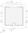
- FIG. 1 is a plan view showing a semiconductor device according to an embodiment of the present disclosure.
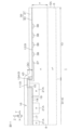
- FIG. 2 is a cross-sectional view taken along the line II-II shown in FIG.
- FIG. 3 is a plan view showing an example of a chip layout.
- FIG. 4 is a perspective view showing an example of a chip layout.
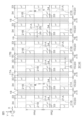
- FIG. 5 is a plan view showing the active area and trench structure.
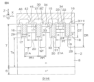
- FIG. 6 is a cross-sectional view taken along the line VI-VI shown in FIG.
- FIG. 7 is a cross-sectional perspective view corresponding to FIG.
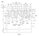
- FIG. 8 is a cross-sectional view taken along line VIII-VIII shown in FIG.
- FIG. 9 is a cross-sectional perspective view corresponding to FIG.
- FIG. 10 is a perspective view showing the configuration of the outer circumferential area.
- FIG. 11 is a cross-sectional view showing a main part of the outer circumferential region.
- FIG. 12 is a schematic diagram showing a wafer used in the manufacture of semiconductor devices.
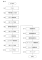
- FIG. 13 is a flowchart showing an example of a method for manufacturing a semiconductor device.
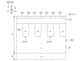
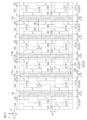
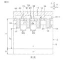
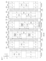
- FIG. 14A is a diagram showing an example of a method for manufacturing a semiconductor device.
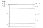
- FIG. 14B is a diagram showing a step subsequent to that of FIG. 14A.
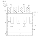
- FIG. 14C is a diagram showing a step subsequent to FIG. 14B.
- FIG. 14D is a diagram showing a step subsequent to FIG. 14C.
- FIG. 14E is a diagram showing a step subsequent to FIG. 14D.
- FIG. 14F is a diagram showing a step subsequent to FIG. 14E.
- FIG. 14A is a diagram showing an example of a method for manufacturing a semiconductor device.
- FIG. 14B is a diagram showing a step subsequent to that of FIG. 14A.
- FIG. 14G is a diagram showing a step subsequent to FIG. 14F.
- FIG. 14H is a diagram showing a step subsequent to FIG. 14G.
- FIG. 15 is a diagram showing a first modification of the semiconductor device.
- 16 is a cross-sectional view taken along the line XVI-XVI shown in FIG. 15.
- FIG. 17 is a diagram showing a second modification of the semiconductor device.
- 18 is a cross-sectional view taken along line XVIII-XVIII shown in FIG. 17.
- FIG. 19 is a diagram showing a third modification of the semiconductor device.
- FIG. 20 is a diagram showing a fourth modification of the semiconductor device.
- FIG. 21 is a diagram showing a fifth modification of the semiconductor device.
- FIG. 22 is a diagram showing a sixth modification of the semiconductor device.
- this term includes a numerical value (shape) that is equal to the numerical value (shape) of the comparison target, as well as a numerical error (shape error) within a range of ⁇ 10% based on the numerical value (shape) of the comparison target.
- shape a numerical value that is equal to the numerical value (shape) of the comparison target
- error a numerical error within a range of ⁇ 10% based on the numerical value (shape) of the comparison target.
- the conductivity type of a semiconductor is indicated using “p-type” or “n-type”, but “p-type” may also be referred to as the “first conductivity type” and “n-type” as the “second conductivity type”. Of course, “n-type” may also be referred to as the “first conductivity type” and “p-type” as the “second conductivity type”.
- p-type is a conductivity type resulting from a trivalent element
- n-type is a conductivity type resulting from a pentavalent element.
- the trivalent element is at least one of boron, aluminum, gallium, and indium.
- the pentavalent element is at least one of nitrogen, phosphorus, arsenic, antimony, and bismuth.
- FIG. 1 is a plan view showing a semiconductor device 1 according to an embodiment.
- FIG. 2 is a cross-sectional view taken along line II-II shown in FIG. 1.
- FIG. 3 is a plan view showing an example layout of a chip 2.
- FIG. 4 is a perspective view showing an example layout of a chip 2.
- FIG. 5 is a plan view showing a trench structure 16 together with an active region 9.
- FIG. 6 is a cross-sectional view taken along line VI-VI shown in FIG. 5.
- FIG. 7 is a cross-sectional perspective view corresponding to FIG. 6.
- FIG. 8 is a cross-sectional view taken along line VIII-VIII shown in FIG. 5.
- FIG. 9 is a cross-sectional perspective view corresponding to FIG. 8.
- the chip 2 has a first main surface 3 on one side, a second main surface 4 on the other side, and first to fourth side surfaces 5A to 5D connecting the first main surface 3 and the second main surface 4.
- the first main surface 3 and the second main surface 4 are formed in a quadrangular shape in a plan view seen from the vertical direction Z (hereinafter simply referred to as "plan view").
- the vertical direction Z is also the thickness direction of the chip 2 and the normal direction of the first main surface 3 (second main surface 4).
- the first main surface 3 and the second main surface 4 may be formed in a square or rectangular shape in a plan view.
- the chip 2 (first main surface 3 and second main surface 4) has an off angle ⁇ o that is inclined at a predetermined angle in a predetermined off direction Do with respect to the c-plane of the SiC single crystal.
- the c-axis ((0001) axis) of the SiC single crystal is inclined by the off angle ⁇ o from the vertical axis toward the off direction Do.
- the c-plane of the SiC single crystal is inclined by the off angle ⁇ o with respect to the horizontal plane.
- the off-direction Do is preferably the a-axis direction of the SiC single crystal (i.e., the second direction Y).
- the off-angle ⁇ o may be greater than 0° and less than or equal to 10°.
- the off-angle ⁇ o may have a value that falls within any one of the following ranges: greater than 0° and less than or equal to 1°, 1° or more and less than or equal to 2.5°, 2.5° or more and less than or equal to 5°, 5° or more and less than or equal to 7.5°, and 7.5° or more and less than or equal to 10°.
- the chip 2 includes an n-type base layer 6 made of SiC single crystal.
- the base layer 6 may also be referred to as a "drain region,” a “base SiC layer,” a “base region,” etc.
- the base layer 6 extends in a layered manner in the horizontal direction and forms part of the second main surface 4 and the first to fourth side surfaces 5A to 5D.
- the base layer 6 is made of a substrate made of SiC single crystal (i.e., a SiC substrate).
- the base layer 6 has the off-direction Do and off-angle ⁇ o described above.
- the base layer 6 may have a peak n-type impurity concentration of 1 ⁇ 10 18 cm ⁇ 3 or more and 1 ⁇ 10 21 cm ⁇ 3 or less.
- the base layer 6 preferably has an almost constant n-type impurity concentration in the thickness direction.
- the n-type impurity concentration of the base layer 6 is preferably adjusted by a single type of pentavalent element. It is particularly preferable that the n-type impurity concentration of the base layer 6 is adjusted by a pentavalent element other than phosphorus. In this embodiment, the n-type impurity concentration of the base layer 6 is adjusted by nitrogen.
- the base layer 6 has a first thickness T1.
- the first thickness T1 may be 5 ⁇ m or more and 300 ⁇ m or less.
- the first thickness T1 may have a value belonging to any one of the following ranges: 5 ⁇ m or more and 50 ⁇ m or less, 50 ⁇ m or more and 100 ⁇ m or less, 100 ⁇ m or more and 150 ⁇ m or less, 150 ⁇ m or more and 200 ⁇ m or less, 200 ⁇ m or more and 250 ⁇ m or less, and 250 ⁇ m or more and 300 ⁇ m or less.
- the first thickness T1 is preferably 50 ⁇ m or more and 250 ⁇ m or less.
- the semiconductor layer 7 has a lower end and an upper end.
- the lower end of the semiconductor layer 7 is the starting point of crystal growth, and the upper end of the semiconductor layer 7 is the end point of crystal growth.
- the lower end of the semiconductor layer 7 is also the bottom of the semiconductor layer 7. Since the semiconductor layer 7 is grown continuously from the base layer 6, the lower end of the semiconductor layer 7 coincides with the upper end of the base layer 6.
- the semiconductor layer 7 includes an n-type drift region 8.
- the drift region 8 is formed by a portion (n-type portion) of the semiconductor layer 7. More specifically, the drift region 8 is formed by a portion of the semiconductor layer 7 on the second main surface 4 side relative to the body region 15 (described below) and the electric field relaxation structures 21A, 21B (described below) in the vertical direction Z.
- the boundary between the base layer 6 and the semiconductor layer 7 is not necessarily visible, but can be indirectly evaluated and/or determined from other configurations and elements.
- the semiconductor layer 7 has an off-direction Do and an off-angle ⁇ o that are approximately the same as the off-direction Do and off-angle ⁇ o of the base layer 6.
- the n-type impurity concentration of the semiconductor layer 7 (drift region 8) is preferably lower than the n-type impurity concentration of the base layer 6.
- the semiconductor layer 7 may have a peak n-type impurity concentration of 1 ⁇ 10 15 cm -3 or more and 1 ⁇ 10 18 cm -3 or less.
- the n-type impurity concentration of the semiconductor layer 7 may be approximately constant in the thickness direction.
- the n-type impurity concentration of the semiconductor layer 7 may have a concentration gradient that gradually increases and/or gradually decreases in the stacking direction (crystal growth direction).
- the n-type impurity concentration of the semiconductor layer 7 is adjusted by nitrogen.
- the semiconductor layer 7 may have an n-type impurity concentration adjusted by at least one pentavalent element.
- the n-type impurity concentration of the semiconductor layer 7 may be adjusted by at least one of nitrogen, phosphorus, arsenic, antimony, and bismuth. It is preferable that the semiconductor layer 7 contains a pentavalent element other than phosphorus.
- the semiconductor layer 7 has a second thickness T2 that is less than the first thickness T1.
- the second thickness T2 may be 1 ⁇ m or more and 10 ⁇ m or less.
- the second thickness T2 may have a value that belongs to any one of the following ranges: 1 ⁇ m or more and 2 ⁇ m or less, 2 ⁇ m or more and 4 ⁇ m or less, 4 ⁇ m or more and 6 ⁇ m or less, 6 ⁇ m or more and 8 ⁇ m or less, and 8 ⁇ m or more and 10 ⁇ m or less.
- the second thickness T2 is preferably 2 ⁇ m or more and 8 ⁇ m or less.
- the semiconductor device 1 includes an active region 9 set in the chip 2.
- the active region 9 is set in the inner part of the chip 2 at a distance from the periphery of the chip 2 (first to fourth side faces 5A to 5D) in a plan view.
- the active region 9 is set in a polygonal shape (a square shape in this embodiment) having four sides parallel to the periphery of the chip 2 in a plan view.
- the planar area of the active region 9 is preferably 50% to 90% of the planar area of the first main surface 3.
- the semiconductor device 1 includes a peripheral region 10 that is set outside the active region 9 in the chip 2.
- the peripheral region 10 is provided in a region between the periphery of the chip 2 and the active region 9 in a planar view.
- the peripheral region 10 extends in a band shape along the active region 9 in a planar view, and is set in a polygonal ring shape (a square ring in this embodiment) that surrounds the active region 9.
- the semiconductor device 1 includes an active surface 11 formed on the first main surface 3, an outer surface 12, and first to fourth connecting surfaces 13A to 13D.
- the active surface 11, outer surface 12, and first to fourth connecting surfaces 13A to 13D define an active plateau 14 on the first main surface 3.
- the active surface 11 may be referred to as the "first surface portion,” the outer peripheral surface 12 as the “second surface portion,” the first to fourth connection surfaces 13A to 13D as the “connection surface portion,” and the active plateau 14 as the “active mesa portion.”
- the active surface 11, the outer peripheral surface 12, and the first to fourth connection surfaces 13A to 13D may be considered to be components of the chip 2 (first main surface 3).
- the active surface 11 is formed in the active region 9. That is, the active surface 11 is formed at a distance inward from the periphery (first to fourth side surfaces 5A to 5D) of the first main surface 3.
- the active surface 11 has a flat surface extending in the first direction X and the second direction Y.
- the active surface 11 is formed by a c-plane (Si-plane).
- the active surface 11 is formed in a quadrangle shape having four sides parallel to the first to fourth side surfaces 5A to 5D in a plan view.
- the outer peripheral surface 12 is formed in the outer peripheral region 10. That is, the outer peripheral surface 12 is formed outside the active surface 11.
- the outer peripheral surface 12 is recessed in the thickness direction of the chip 2 (towards the second main surface 4) relative to the active surface 11. Specifically, in this embodiment, the outer peripheral surface 12 is recessed to a depth less than the thickness of the semiconductor layer 7 so as to expose the semiconductor layer 7. That is, the outer peripheral surface 12 faces the base layer 6 with a portion of the semiconductor layer 7 in between, exposing the semiconductor layer 7.
- the outer peripheral surface 12 extends in a band shape along the active surface 11 in a plan view, and is formed in a ring shape (specifically, a square ring shape) surrounding the active surface 11.
- the outer peripheral surface 12 has a flat surface extending in the first direction X and the second direction Y, and is formed approximately parallel to the active surface 11.
- the outer peripheral surface 12 is formed by a c-plane (Si-plane).
- the outer peripheral surface 12 is connected to the first to fourth side surfaces 5A to 5D.
- the outer peripheral surface 12 has an outer peripheral depth DO.
- the outer peripheral depth DO may be 0.1 ⁇ m or more and 2 ⁇ m or less.
- the outer peripheral depth DO may have a value that falls within any one of the following ranges: 0.1 ⁇ m or more and 0.25 ⁇ m or less, 0.25 ⁇ m or more and 0.5 ⁇ m or less, 0.5 ⁇ m or more and 0.75 ⁇ m or less, 0.75 ⁇ m or more and 1 ⁇ m or less, 1 ⁇ m or more and 1.5 ⁇ m or less, and 1.5 ⁇ m or more and 2 ⁇ m or less.
- the outer peripheral depth DO is preferably 0.1 ⁇ m or more and 1.5 ⁇ m or less.
- the first to fourth connection surfaces 13A to 13D extend in the vertical direction Z and connect the active surface 11 and the outer peripheral surface 12.
- the first connection surface 13A is located on the first side surface 5A side
- the second connection surface 13B is located on the second side surface 5B side
- the third connection surface 13C is located on the third side surface 5C side
- the fourth connection surface 13D is located on the fourth side surface 5D side.
- the first connection surface 13A and the third connection surface 13C extend in the first direction X and face the second direction Y.
- the second connection surface 13B and the fourth connection surface 13D extend in the second direction Y and face the first direction X.
- the first to fourth connection faces 13A to 13D may extend substantially perpendicularly between the active surface 11 and the outer peripheral surface 12 so as to define a quadrangular prism-shaped active plateau 14.
- the first to fourth connection faces 13A to 13D may be inclined obliquely downward from the active surface 11 toward the outer peripheral surface 12 so as to define a quadrangular pyramid-shaped active plateau 14.
- the active plateau 14 is defined in a protruding shape on the semiconductor layer 7 at the first main surface 3.
- the active plateau 14 is formed only on the semiconductor layer 7, and is not formed on the base layer 6.
- the semiconductor device 1 includes a p-type body region 15 formed in a surface layer portion of the first main surface 3 (active surface 11).
- the body region 15, which is an example of a second impurity region, is formed in a layer extending along the active surface 11.
- the body region 15 may be formed over the entire active surface 11 and exposed from the first to fourth connection surfaces 13A to 13D.
- the body region 15 is formed at a distance from the lower end of the semiconductor layer 7 toward the active surface 11. It is preferable that the body region 15 is formed at a distance from the depth position of the outer peripheral surface 12 toward the active surface 11 and exposed from the active surface 11.
- the body region 15 may have a peak p-type impurity concentration of 1 ⁇ 10 15 cm ⁇ 3 or more and 1 ⁇ 10 18 cm ⁇ 3 or less.
- the p-type impurity concentration of the body region 15 is preferably adjusted by at least one trivalent element.
- the trivalent element of the body region 15 may be at least one of boron, aluminum, gallium, and indium.
- the semiconductor device 1 includes a plurality of trench electrode type trench structures 16 formed on the first main surface 3 (active surface 11) in the active region 9.
- the trench structures 16 may be referred to as "gate structures", “trench gate structures”, etc.
- a gate potential is applied to the plurality of trench structures 16 as a control potential.
- the plurality of trench structures 16 control the inversion and non-inversion of the channel (current path) in the body region 15 in response to the gate potential.
- the multiple trench structures 16 are arranged at intervals inward from the periphery (first to fourth connection surfaces 13A to 13D) of the active surface 11 in the active region 9.
- the multiple trench structures 16 are arranged at intervals in the first direction X, and are each formed in a strip shape extending in the second direction Y.
- the multiple trench structures 16 are arranged at intervals in the m-axis direction and each extends in the a-axis direction.
- the multiple trench structures 16 are arranged in stripes extending in the a-axis direction (second direction Y).
- the extension direction of the multiple trench structures 16 coincides with the off-direction Do of the semiconductor layer 7.
- the multiple trench structures 16 are formed at intervals from the lower end (base layer 6) of the semiconductor layer 7 toward the first main surface 3 (active surface 11), and face the base layer 6 with a portion of the semiconductor layer 7 in between.
- the multiple trench structures 16 define a lower region 7a in the region between the bottom walls of the multiple trench structures 16 and the lower end (base layer 6) of the semiconductor layer 7.
- Each trench structure 16 has a trench width WT in the arrangement direction and a trench depth DT in the vertical direction Z.
- the trench width WT is preferably less than the second thickness T2 of the semiconductor layer 7.
- the trench width WT may be 0.1 ⁇ m or more and 5 ⁇ m or less.
- the insulating film 18 covers the wall surface of the trench 17.
- the insulating film 18 may include at least one of a silicon oxide film, a silicon nitride film, and a silicon oxynitride film.
- the insulating film 18 has a single-layer structure made of a silicon oxide film. It is particularly preferable that the insulating film 18 includes a silicon oxide film made of an oxide of the chip 2.
- the buried electrode 19 is buried in the trench 17 and faces the channel across the insulating film 18. In this embodiment, the buried electrode 19 faces the body region 15 across the insulating film 18.
- the buried electrode 19 may include p-type or n-type conductive polysilicon.
- the multiple first electric field relaxation structures 21A are arranged at intervals in the first direction X in the lower region 7a, and are also arranged at intervals in the second direction Y.
- Each first electric field relaxation structure 21A may be formed in a rectangular shape in a plan view.
- the multiple first electric field relaxation structures 21A are arranged at intervals in the m-axis direction, and are also arranged at intervals in the a-axis direction of the SiC single crystal.
- the first relaxation pitch PR1 and the second relaxation pitch PR2 may have a value that falls within any one of the ranges of 0.25 ⁇ m to 0.5 ⁇ m, 0.5 ⁇ m to 0.75 ⁇ m, 0.75 ⁇ m to 1 ⁇ m, 1 ⁇ m to 1.5 ⁇ m, 1.5 ⁇ m to 2 ⁇ m, 2 ⁇ m to 2.5 ⁇ m, 2.5 ⁇ m to 3 ⁇ m, 3 ⁇ m to 3.5 ⁇ m, 3.5 ⁇ m to 4 ⁇ m, 4 ⁇ m to 4.5 ⁇ m, and 4.5 ⁇ m to 5 ⁇ m.
- the first relaxation pitch PR1 and the second relaxation pitch PR2 are preferably 0.5 ⁇ m to 3.0 ⁇ m.
- Each first electric field relaxation structure 21A is formed integrally with the body region 15 and is formed on one side of the trench 17 in the first direction X.
- each first electric field relaxation structure 21A extends from a part of the body region 15 between two adjacent trenches 17 downward in the vertical direction Z below the bottom wall of the trench 17, and spreads in the horizontal direction along the first main surface 3, overlapping the bottom wall of the trench 17.
- Each first electric field relaxation structure 21A covers the bottom wall of the trench 17.
- each first electric field relaxation structure 21A forms at least a portion of one of the side walls and bottom wall of a pair of opposing trenches 17, and is in contact with the insulating film 18.
- Each first electric field relaxation structure 21A has a substantially L-shaped exposed surface that is exposed within each trench 17 as the lower part of the side wall of the trench 17 and the bottom wall of the trench 17 that is continuous with the lower part of the side wall.
- the second electric field relaxation structures 21B are arranged at intervals in the first direction X in the lower region 7a, and are also arranged at intervals in the second direction Y.
- Each second electric field relaxation structure 21B may be formed in a rectangular shape in a plan view.
- the second electric field relaxation structures 21B are arranged at intervals in the m-axis direction, and are also arranged at intervals in the a-axis direction of the SiC single crystal.
- the second electric field relaxation structures 21B are arranged in the first direction X at intervals of a third relaxation pitch PR3.
- the third relaxation pitch PR3 may be the same as the first relaxation pitch PR1 and the trench pitch PT.
- the second electric field relaxation structures 21B are arranged in the second direction Y at intervals of a fourth relaxation pitch PR4.
- the fourth relaxation pitch PR4 may be the same as the second relaxation pitch PR2 and the third relaxation pitch PR3.
- the third relaxation pitch PR3 and the fourth relaxation pitch PR4 may have a value that falls within any one of the ranges of 0.25 ⁇ m to 0.5 ⁇ m, 0.5 ⁇ m to 0.75 ⁇ m, 0.75 ⁇ m to 1 ⁇ m, 1 ⁇ m to 1.5 ⁇ m, 1.5 ⁇ m to 2 ⁇ m, 2 ⁇ m to 2.5 ⁇ m, 2.5 ⁇ m to 3 ⁇ m, 3 ⁇ m to 3.5 ⁇ m, 3.5 ⁇ m to 4 ⁇ m, 4 ⁇ m to 4.5 ⁇ m, and 4.5 ⁇ m to 5 ⁇ m.
- the third relaxation pitch PR3 and the fourth relaxation pitch PR4 are preferably 0.5 ⁇ m to 3.0 ⁇ m.
- Each second electric field relaxation structure 21B is formed integrally with the body region 15 and is formed on the other side of the trench 17 in the first direction X.
- each second electric field relaxation structure 21B extends from a part of the body region 15 between two adjacent trenches 17 downward in the vertical direction Z below the bottom wall of the trench 17, and spreads in the horizontal direction along the first main surface 3, overlapping the bottom wall of the trench 17.
- Each second electric field relaxation structure 21B covers the bottom wall of the trench 17.
- each second electric field relaxation structure 21B forms at least a portion of the other sidewall (the sidewall opposite the first electric field relaxation structure 21A) and bottom wall of a pair of opposing trenches 17, and is in contact with the insulating film 18.
- Each second electric field relaxation structure 21B has a substantially L-shaped exposed surface that is exposed within each trench 17 as the lower part of the sidewall of the trench 17 and the bottom wall of the trench 17 that is continuous with the lower part of the sidewall.
- first electric field relaxation structures 21A and a plurality of second electric field relaxation structures 21B are alternately arranged along the second direction Y.
- first electric field relaxation structures 21A protruding from each trench 17 to one side in the first direction X and the second electric field relaxation structures 21B protruding to the other side of the first direction X (the opposite side to the first electric field relaxation structures 21A) are alternately arranged along the second direction Y.
- first trench 17A For convenience, in FIG. 5, a pair of adjacent trenches 17 from among the multiple trenches 17 is selectively picked out, and one trench 17 is shown as a first trench 17A, and the other trench 17 is shown as a first trench 17B.
- first trench 17A For convenience, in FIG. 5, a pair of adjacent trenches 17 from among the multiple trenches 17 is selectively picked out, and one trench 17 is shown as a first trench 17A, and the other trench 17 is shown as a first trench 17B.
- first trench 17A, 17B may also be defined as first trenches 17A, 17B.
- the second electric field relief structure 21B of the first trench 17B is disposed adjacent in the first direction X to the region between the multiple first electric field relief structures 21A of the first trench 17A.
- the first electric field relief structure 21A of the first trench 17B is disposed adjacent in the first direction X to the region between the multiple second electric field relief structures 21B of the first trench 17B.
- the multiple first electric field relief structures 21A of the first trench 17A and the multiple second electric field relief structures 21B of the first trench 17B are arranged alternately along the second direction Y.
- the multiple first electric field relief structures 21A of the first trench 17A and the multiple second electric field relief structures 21B of the first trench 17B may not overlap in the second direction Y as shown in FIG. 5, or may partially overlap each other.
- each of the first trenches 17A and 17B the multiple first electric field relaxation structures 21A and the multiple second electric field relaxation structures 21B are arranged without any gaps along the second direction Y.
- the multiple first electric field relaxation structures 21A of the first trench 17A and the multiple second electric field relaxation structures 21B of the first trench 17B are arranged without any gaps along the second direction Y.
- the end of each first electric field relaxation structure 21A of the first trench 17A in the second direction Y may be aligned in a straight line along the first direction X with the end of each second electric field relaxation structure 21B of the first trench 17B in the second direction Y.
- each first electric field relaxation structure 21A of the first trench 17A may partially overlap with each second electric field relaxation structure 21B of the first trench 17B in the first direction X.
- the first electric field relief structures 21A of the multiple trenches 17 are linearly arranged along the first direction X.
- the second electric field relief structures 21B of the multiple trenches 17 are linearly arranged along the first direction X.
- the multiple first electric field relief structures 21A and the multiple second electric field relief structures 21B are arranged overall in a staggered pattern in a planar view.
- the body region 15 includes a channel portion 22 and a non-channel portion 23.
- the channel portion 22 is physically separated from the first electric field relaxation structure 21A and the second electric field relaxation structure 21B.
- a channel is formed along the wall surface of the trench 17 adjacent to the channel portion 22.
- the non-channel portion 23 is physically integrated with the first electric field relaxation structure 21A and the second electric field relaxation structure 21B.
- the non-channel portion 23 has a bottom wall covered from below by the first electric field relaxation structure 21A and the second electric field relaxation structure 21B.
- the multiple first electric field relaxation structures 21A of the first trench 17A and the multiple second electric field relaxation structures 21B of the first trench 17B are arranged without any gaps in the second direction Y.
- the multiple channel portions 22 are arranged in a zigzag pattern in the second direction Y.
- the channel portion 22 along the first trench 17A is sandwiched between a pair of first electric field relaxation structures 21A in the second direction Y, and is sandwiched between the first trench 17A and the second electric field relaxation structure 21B of the first trench 17B in the first direction X.
- the channel portion 22 along the first trench 17B is sandwiched between a pair of second electric field relaxation structures 21B in the second direction Y, and is sandwiched between the first trench 17B and the first electric field relaxation structure 21A of the first trench 17A in the first direction X.
- each channel portion 22 is surrounded on three sides by a plurality of electric field relaxation structures 21A, 21B formed as diffusion regions that are physically independent of each other, and is adjacent to the trench 17 on the remaining side.
- the first electric field relaxation structure 21A and the second electric field relaxation structure 21B form a boundary portion 24 between the bottom of the non-channel portion 23 between adjacent trenches 17.
- the boundary portion 24 divides the mesa portion 20 into the body region 15 (non-channel portion 23) on the first main surface 3 side and the electric field relaxation structures 21A and 21B on the second main surface 4 side.
- the boundary portion 24 does not need to be clearly defined by image analysis (e.g., SEM image analysis, etc.) because both the body region 15 (non-channel portion 23) and the electric field relaxation structures 21A, 21B are p-type.
- image analysis e.g., SEM image analysis, etc.
- the fact that the body region 15 and the electric field relaxation structures 21A, 21B are continuous in the vertical direction Z may be confirmed, for example, by obtaining a profile of the p-type impurity concentration in the vertical direction Z from the first main surface 3 to the second main surface 4.
- each electric field relaxation structure 21A, 21B may integrally have a base portion 28 on the second main surface 4 side of the bottom wall of the trench 17, and a protrusion portion 29 sandwiched between two adjacent trenches 17.
- the base portion 28 overlaps each trench 17 and crosses the sidewall of each trench 17 in the first direction X.
- the base portion 28 has an end that protrudes horizontally outward beyond the area directly below the mesa portion 20.
- the protrusions 29 extend from the base 28 along the side walls of each trench 17 to the inside of the mesa portion 20 and are connected to the bottom of the body region 15.
- the protrusions 29 are formed from the bottom wall of the trench 17 in the vertical direction Z to the body region 15.
- each of the electric field relaxation structures 21A and 21B may have an end 30 at the center of the bottom wall of the trench 17 in the width direction of the trench 17.
- the bottom wall of the trench 17 may have a first portion 31 formed on the non-channel portion 23 side in the width direction of the trench 17 and covered by the electric field relaxation structures 21A and 21B.
- the bottom wall of the trench 17 may also have a second portion 32 formed on the channel portion 22 side with respect to the first portion 31 and covered by the semiconductor layer 7 (drift region 8). Since the portion of the bottom wall of the trench 17 on the channel portion 22 side is covered by the drift region 8, a current path can be sufficiently secured along the wall surface (side wall and bottom wall) of the trench 17 on the channel portion 22 side. As a result, the on-resistance can be reduced.
- the p-type impurity concentration of the electric field relaxation structures 21A, 21B is preferably higher than the p-type impurity concentration of the body region 15.
- the electric field relaxation structures 21A, 21B may have a peak p-type impurity concentration of 1 ⁇ 10 18 cm ⁇ 3 or more and 1 ⁇ 10 20 cm ⁇ 3 or less.
- the p-type impurity concentration of the electric field relaxation structures 21A, 21B may be approximately constant in the thickness direction.
- the p-type impurity concentration of the electric field relaxation structures 21A, 21B may have a concentration gradient that gradually increases and/or gradually decreases in the stacking direction (crystal growth direction).
- the first mask 60 is removed (step S6 in FIG. 13).
- a process for forming a plurality of source regions 33 is carried out (step S7 in FIG. 13).
- the plurality of source regions 33 are formed by introducing n-type impurities into the surface layer of the semiconductor layer 7 by ion implantation through a mask (not shown) having a predetermined layout.
- the multiple first electric field relaxation structures 21A of the first trench 17A and the multiple second electric field relaxation structures 21B of the first trench 17B are arranged without any gaps in the second direction Y. This allows the multiple first electric field relaxation structures 21A and the multiple second electric field relaxation structures 21B to be densely arranged close to each other, further improving the electric field relaxation effect.
- the portion of the body region 15 that is physically integrated with the electric field relaxation structures 21A, 21B is covered with the second conductivity type portion (body region 15 and electric field relaxation structures 21A, 21B) from the sidewall to the bottom wall of the trench 17. Since the range in which an inversion layer should be formed along the inner wall of the trench 17 is long, the voltage (threshold voltage) required to form a channel tends to be selectively higher than that of the channel portion 22. Therefore, by making the portion of the body region 15 that is physically integrated with the electric field relaxation structures 21A, 21B into a non-channel portion 23, it is possible to suppress variation in the threshold voltage of the semiconductor device 1.
- FIGS. 15 to 22 are diagrams showing first to sixth modified examples of the semiconductor device 1. Next, the modified examples of the semiconductor device 1 will be described with reference to FIGS. 15 to 22.
- each of the first trenches 17A, 17B the multiple first electric field relaxation structures 21A and the multiple second electric field relaxation structures 21B are arranged at intervals along the second direction Y.
- the multiple first electric field relaxation structures 21A of the first trench 17A and the multiple second electric field relaxation structures 21B of the first trench 17B are arranged at intervals in the second direction Y.
- each first electric field relaxation structure 21A of the first trench 17A does not overlap with each second electric field relaxation structure 21B of the first trench 17B in the first direction X.
- a channel section 27 is formed in which neither the first electric field relaxation structure 21A nor the second electric field relaxation structure 21B is formed.
- the channel section 27 is a region having a constant width in the second direction Y.
- a source region 33 is formed on the sidewall of the trench 17 on both sides of the mesa portion 20 in the first direction X.
- the contact region 34 (first portion 25) is sandwiched between a pair of source regions 33 in the first direction X.
- a plurality of source regions 33 are arranged at intervals in the extension direction of the trench structure 16 on both sides of the first direction X.
- the source region 33 on one side and the source region 33 on the other side each have an end in the channel section 27 and partially overlap in the first direction X.
- the source region 33 on one side and the source region 33 on the other side are formed so as not to overlap in the first direction X.
- a channel section 27 is formed by arranging a plurality of first electric field relaxation structures 21A and a plurality of second electric field relaxation structures 21B at intervals along the second direction Y.
- a channel can be formed on the side walls of the trench 17 on both sides of the mesa portion 20 in the first direction X.
- the channel density in each mesa portion 20 can be improved.
- electric field concentration on the insulating film 18 of the trench 17 can be effectively alleviated, and the channel density can be improved.
- the first electric field relaxation structure 21A of the first trench 17A and the second electric field relaxation structure 21B of the first trench 17B are integrated to form a single electric field relaxation structure 35 spanning the first trench 17A and the first trench 17B.
- the electric field relaxation structures 35 are arranged in a staggered pattern in plan view.
- the multiple mesa portions 20 are defined as alternating first mesa portions 20A and second mesa portions 20B in the first direction X.
- first electric field relaxation structures are arranged at intervals in the extension direction of the trench structure 16.
- second electric field relaxation structures are arranged at intervals in the extension direction of the trench structure 16.
- the multiple electric field relaxation structures 35A and the multiple electric field relaxation structures 35B are arranged so as not to overlap each other in the first direction X.
- the multiple electric field relaxation structures 35A and the multiple electric field relaxation structures 35B are arranged in a staggered pattern as a whole.
- each mesa portion 20A, 20B the region where the multiple electric field relaxation structures 35A, 35B are not formed is the channel section 36.
- the channel section 36 is a region having a constant width in the second direction Y.
- the region where the multiple electric field relaxation structures 35A, 35B are formed is the non-channel section 48.
- the non-channel section 48 is a region having a constant width in the second direction Y.
- the channel sections 36 and non-channel sections 48 are arranged alternately in the extension direction of the trench structure 16.
- the source region 33 is formed on the sidewall of the trench 17 on both sides of the mesa portions 20A and 20B in the first direction X.
- the contact region 34 (first portion 25) is sandwiched between a pair of source regions 33 in the first direction X.
- the contact region 34 is formed over the entire first main surface 3 between the trench structure 16 on one side of the mesa portions 20A and 20B and the trench structure 16 on the other side. In other words, in the non-channel section 48, the contact region 34 crosses the mesa portions 20A and 20B from the trench structure 16 on one side of the mesa portions 20A and 20B to the trench structure 16 on the other side.
- electric field relaxation structures 35A, 35B are formed around the channel section 36 on the top, bottom, left and right sides of the page.
- the electric field can be relaxed from the top, bottom, left and right of each channel section 36, improving the effect of relaxing the electric field concentration in the insulating film 18 of the trench 17.
- the channel sections 36 and non-channel sections 48 are arranged alternately along the extension direction of the trench structure 16, and are clearly partitioned. This allows the function of the channel sections 36, which form a current path, to be separated from the function of the non-channel sections 48, which ensure electrical contact with the body region 15. As a result, an efficient ON operation can be achieved.
- each electric field relaxation structure 21A, 21B may have an end 30 at the position of the wall surface (sidewall) of trench 17 in the width direction of trench 17.
- the wall surface (sidewall) of trench 17 and the end 30 of electric field relaxation structure 21A, 21B may be linearly continuous in the vertical direction Z.
- each electric field relaxation structure 21A, 21B may be a curved surface that bulges in the horizontal direction (at least one of the first direction X and the second direction Y) rather than being a flat surface that is parallel or approximately parallel to the vertical direction Z from the bottom wall of the trench 17.
- the element structure of the semiconductor device 1 may be an IGBT (Insulated Gate Bipolar Transistor) structure, unlike the MISFET structure of FIGS. 6 to 9.
- a p-type collector region 71 may be formed instead of the base layer 6.
- a p-type base region 72 may be formed by the body region 15, and an n-type emitter region 73 may be formed by the source region 33.
- each channel portion 22 is sandwiched between electric field relaxation structures 21A, 21B on both sides in the first direction X and the second direction Y, and is surrounded by the electric field relaxation structures 21A, 21B.
- the electric field can be relaxed from above, below, left and right of each channel portion 22, improving the effect of relaxing the electric field concentration in the insulating film 18 of the trench 17 of the trench gate structure related to the IGBT.
- the trench 17 may include a second trench 17C in which the electric field relaxation structures 21A, 21B are not formed.
- the electric field relaxation structures 21A, 21B it is not necessary for the electric field relaxation structures 21A, 21B to be formed in all of the multiple trenches 17 formed in the chip 2, and the electric field relaxation structures 21A, 21B may not be formed in some of the trenches 17 (second trenches 17C).
- the base layer 6 and the semiconductor layer 7 each contain a SiC single crystal.
- at least one or all of the base layer 6 and the semiconductor layer 7 may contain a single crystal of a wide band gap semiconductor other than a SiC single crystal.
- a wide band gap semiconductor is a semiconductor having a band gap larger than that of silicon.
- Examples of single crystals of wide band gap semiconductors include silicon carbide (SiC), gallium nitride (GaN), diamond (C), and gallium oxide (Ga 2 O 3 ).
- the base layer 6 and the semiconductor layer 7 may be made of the same type of single crystal, or may be made of different types of single crystal. At least one or all of the base layer 6 and the semiconductor layer 7 may be made of silicon (Si).
- semiconductor device in the following items may be replaced with "SiC semiconductor device,” “wide band gap semiconductor device,” “semiconductor switching device,” “semiconductor rectifier device,” “MISFET device,” “IGBT device,” “diode device,” etc., as necessary.
- the first electric field relaxation structure (21A) and the second electric field relaxation structure (21B) are formed on the bottom wall of the first trench (17A, 17B), so that the electric field concentration on the bottom wall of the trench (17A, 17B) can be relaxed.
- the multiple first electric field relaxation structures (21A) and the multiple second electric field relaxation structures (21B) are arranged alternately along the second direction (Y). This allows the electric field in the area adjacent to the first electric field relaxation structure (21A) and the second electric field relaxation structure (21B) to be relaxed from above, below, left, and right, so that the electric field concentration on the trench (17A, 17B) can be effectively relaxed.
- Appendix 1-2 A pair of the first trenches (17A, 17B) are adjacent to each other in the first direction (X), The semiconductor device (1) described in Appendix 1-1, wherein the second electric field relaxation structure (21B) of the other first trench (17B) is disposed at a position adjacent in the first direction (X) to a region between the plurality of first electric field relaxation structures (21A) of one of the pair of first trenches (17A, 17B).
- Appendix 1-3 The semiconductor device (1) described in Appendix 1-2, wherein the first electric field relaxation structure (21A) of the one first trench (17A) and the first electric field relaxation structure (21A) of the other first trench (17B) are linearly arranged along the first direction (X).
- Appendix 1-4 The semiconductor device (1) described in Appendix 1-2 or Appendix 1-3, wherein in each of the first trenches (17A, 17B), the plurality of first electric field relaxation structures (21A) and the plurality of second electric field relaxation structures (21B) are arranged without any gaps along the second direction (Y).
- the multiple first electric field relaxation structures (21A) and the multiple second electric field relaxation structures (21B) can be densely arranged close to each other, further improving the electric field relaxation effect.
- This configuration effectively reduces electric field concentration in the trenches (17A, 17B) and improves channel density.
- Appendix 1-6 A pair of the first trenches (17A, 17B) are adjacent to each other in the first direction (X), The semiconductor device (1) described in Appendix 1-1, wherein the first electric field relaxation structure (21A) of one of the pair of first trenches (17A, 17B) and the second electric field relaxation structure (21B) of the other of the pair of first trenches (17A, 17B) are integrated to form a single electric field relaxation structure (35) spanning the one first trench (17A) and the other first trench (17B).
- the semiconductor device (1) according to any one of Appendices 1-1 to 1-6, wherein the second impurity region (15, 72) includes a channel portion (22) physically separated from the first electric field relaxation structure (21A) and the second electric field relaxation structure (21B), in which a channel is formed along the first trench (17A, 17B), and a non-channel portion (23) that is physically integrated with the first electric field relaxation structure (21A) and the second electric field relaxation structure (21B) and has a bottom wall covered by the first electric field relaxation structure (21A) and the second electric field relaxation structure (21B).
- the second impurity region (15, 72) includes a channel portion (22) physically separated from the first electric field relaxation structure (21A) and the second electric field relaxation structure (21B), in which a channel is formed along the first trench (17A, 17B), and a non-channel portion (23) that is physically integrated with the first electric field relaxation structure (21A) and the second electric field relaxation structure (21B) and has a bottom wall covered by the first electric field relaxation structure (21
- the portion of the second impurity region (15, 72) that is physically integrated with the first electric field relaxation structure (21A) and the second electric field relaxation structure (21B) is covered with the second conductivity type portion (the second impurity region (15, 72), and the first electric field relaxation structure (21A) and the second electric field relaxation structure (21B)) from the side wall to the bottom wall of the trench (17). Since the range in which the inversion layer should be formed along the inner wall of the trench (17) is long, the voltage (threshold voltage) required for channel formation tends to be selectively high in that portion.
- the third impurity region (33, 73) is selectively formed in the channel portion (22) of the channel portion (22) and the non-channel portion (23); a fourth impurity region (34) of a second conductivity type formed in a surface layer portion of the second impurity region (15, 72) and having a higher impurity concentration than the second impurity region (15, 72);
- Appendix 1-11 a drain region (6) of a first conductivity type formed on the second main surface (4) side of the first impurity region (7); a body region (15) formed by the second impurity region (15, 72); a source region (33) formed by the third impurity region (33, 73);
- the semiconductor device (1) according to any one of Appendices 1-1 to 1-10, comprising a trench gate structure (16) formed by the trench (17), an insulating film (18) covering a wall surface of the trench (17), and a buried electrode (19) buried in the trench (17).
Landscapes
- Electrodes Of Semiconductors (AREA)
Priority Applications (1)
| Application Number | Priority Date | Filing Date | Title |
|---|---|---|---|
| JP2025533908A JPWO2025018064A1 (https=) | 2023-07-20 | 2024-06-12 |
Applications Claiming Priority (2)
| Application Number | Priority Date | Filing Date | Title |
|---|---|---|---|
| JP2023118661 | 2023-07-20 | ||
| JP2023-118661 | 2023-07-20 |
Publications (1)
| Publication Number | Publication Date |
|---|---|
| WO2025018064A1 true WO2025018064A1 (ja) | 2025-01-23 |
Family
ID=94281371
Family Applications (1)
| Application Number | Title | Priority Date | Filing Date |
|---|---|---|---|
| PCT/JP2024/021287 Pending WO2025018064A1 (ja) | 2023-07-20 | 2024-06-12 | 半導体装置 |
Country Status (2)
| Country | Link |
|---|---|
| JP (1) | JPWO2025018064A1 (https=) |
| WO (1) | WO2025018064A1 (https=) |
Citations (3)
| Publication number | Priority date | Publication date | Assignee | Title |
|---|---|---|---|---|
| WO2018225600A1 (ja) * | 2017-06-06 | 2018-12-13 | 三菱電機株式会社 | 半導体装置および電力変換装置 |
| JP2019096711A (ja) * | 2017-11-22 | 2019-06-20 | 株式会社東芝 | 半導体装置、半導体装置の製造方法、インバータ回路、駆動装置、車両、及び、昇降機 |
| JP2020017641A (ja) * | 2018-07-26 | 2020-01-30 | 株式会社東芝 | 半導体装置、インバータ回路、駆動装置、車両、及び、昇降機 |
-
2024
- 2024-06-12 WO PCT/JP2024/021287 patent/WO2025018064A1/ja active Pending
- 2024-06-12 JP JP2025533908A patent/JPWO2025018064A1/ja active Pending
Patent Citations (3)
| Publication number | Priority date | Publication date | Assignee | Title |
|---|---|---|---|---|
| WO2018225600A1 (ja) * | 2017-06-06 | 2018-12-13 | 三菱電機株式会社 | 半導体装置および電力変換装置 |
| JP2019096711A (ja) * | 2017-11-22 | 2019-06-20 | 株式会社東芝 | 半導体装置、半導体装置の製造方法、インバータ回路、駆動装置、車両、及び、昇降機 |
| JP2020017641A (ja) * | 2018-07-26 | 2020-01-30 | 株式会社東芝 | 半導体装置、インバータ回路、駆動装置、車両、及び、昇降機 |
Also Published As
| Publication number | Publication date |
|---|---|
| JPWO2025018064A1 (https=) | 2025-01-23 |
Similar Documents
| Publication | Publication Date | Title |
|---|---|---|
| US11004936B2 (en) | Silicon carbide insulated-gate power field effect transistor | |
| WO2025143233A1 (ja) | 半導体装置 | |
| WO2025018064A1 (ja) | 半導体装置 | |
| WO2024143378A1 (ja) | SiC半導体装置 | |
| WO2024101131A1 (ja) | SiC半導体装置 | |
| WO2025004543A1 (ja) | 半導体装置 | |
| WO2025018065A1 (ja) | 半導体装置 | |
| WO2023189054A1 (ja) | 半導体装置 | |
| US20260020325A1 (en) | Semiconductor device | |
| US20260090057A1 (en) | Semiconductor device and method for manufacturing same | |
| US20260032949A1 (en) | Semiconductor device and manufacturing method for semiconductor device | |
| US20260020303A1 (en) | Semiconductor device | |
| US20260090037A1 (en) | Sic semiconductor device | |
| WO2025023129A1 (ja) | 半導体装置 | |
| WO2025177996A1 (ja) | 半導体装置 | |
| WO2025023128A1 (ja) | 半導体装置 | |
| WO2024195461A1 (ja) | 半導体装置および半導体装置の製造方法 | |
| WO2025074763A1 (ja) | 半導体装置 | |
| WO2025177995A1 (ja) | 半導体装置 | |
| WO2025197728A1 (ja) | 半導体装置 | |
| WO2025013769A1 (ja) | 半導体装置 | |
| WO2026058816A1 (ja) | 半導体装置 | |
| WO2025225306A1 (ja) | 半導体装置 | |
| WO2024203339A1 (ja) | 半導体装置 | |
| WO2026018786A1 (ja) | 半導体装置 |
Legal Events
| Date | Code | Title | Description |
|---|---|---|---|
| ENP | Entry into the national phase |
Ref document number: 2025533908 Country of ref document: JP Kind code of ref document: A |
|
| WWE | Wipo information: entry into national phase |
Ref document number: 2025533908 Country of ref document: JP |
|
| NENP | Non-entry into the national phase |
Ref country code: DE |