WO2025017976A1 - 圧電振動素子 - Google Patents
圧電振動素子 Download PDFInfo
- Publication number
- WO2025017976A1 WO2025017976A1 PCT/JP2024/013407 JP2024013407W WO2025017976A1 WO 2025017976 A1 WO2025017976 A1 WO 2025017976A1 JP 2024013407 W JP2024013407 W JP 2024013407W WO 2025017976 A1 WO2025017976 A1 WO 2025017976A1
- Authority
- WO
- WIPO (PCT)
- Prior art keywords
- excitation electrode
- outer edge
- edge portion
- velocity region
- region
- Prior art date
- Legal status (The legal status is an assumption and is not a legal conclusion. Google has not performed a legal analysis and makes no representation as to the accuracy of the status listed.)
- Pending
Links
Images


Classifications
-
- H—ELECTRICITY
- H03—ELECTRONIC CIRCUITRY
- H03H—IMPEDANCE NETWORKS, e.g. RESONANT CIRCUITS; RESONATORS
- H03H9/00—Networks comprising electromechanical or electro-acoustic elements; Electromechanical resonators
- H03H9/15—Constructional features of resonators consisting of piezoelectric or electrostrictive material
- H03H9/17—Constructional features of resonators consisting of piezoelectric or electrostrictive material having a single resonator
- H03H9/19—Constructional features of resonators consisting of piezoelectric or electrostrictive material having a single resonator consisting of quartz
-
- H—ELECTRICITY
- H03—ELECTRONIC CIRCUITRY
- H03H—IMPEDANCE NETWORKS, e.g. RESONANT CIRCUITS; RESONATORS
- H03H9/00—Networks comprising electromechanical or electro-acoustic elements; Electromechanical resonators
- H03H9/02—Details
- H03H9/02007—Details of bulk acoustic wave devices
- H03H9/02157—Dimensional parameters, e.g. ratio between two dimension parameters, length, width or thickness
-
- H—ELECTRICITY
- H03—ELECTRONIC CIRCUITRY
- H03H—IMPEDANCE NETWORKS, e.g. RESONANT CIRCUITS; RESONATORS
- H03H9/00—Networks comprising electromechanical or electro-acoustic elements; Electromechanical resonators
- H03H9/02—Details
- H03H9/125—Driving means, e.g. electrodes, coils
- H03H9/13—Driving means, e.g. electrodes, coils for networks consisting of piezoelectric or electrostrictive materials
- H03H9/132—Driving means, e.g. electrodes, coils for networks consisting of piezoelectric or electrostrictive materials characterized by a particular shape
-
- H—ELECTRICITY
- H10—SEMICONDUCTOR DEVICES; ELECTRIC SOLID-STATE DEVICES NOT OTHERWISE PROVIDED FOR
- H10N—ELECTRIC SOLID-STATE DEVICES NOT OTHERWISE PROVIDED FOR
- H10N30/00—Piezoelectric or electrostrictive devices
- H10N30/20—Piezoelectric or electrostrictive devices with electrical input and mechanical output, e.g. functioning as actuators or vibrators
-
- H—ELECTRICITY
- H10—SEMICONDUCTOR DEVICES; ELECTRIC SOLID-STATE DEVICES NOT OTHERWISE PROVIDED FOR
- H10N—ELECTRIC SOLID-STATE DEVICES NOT OTHERWISE PROVIDED FOR
- H10N30/00—Piezoelectric or electrostrictive devices
- H10N30/80—Constructional details
- H10N30/87—Electrodes or interconnections, e.g. leads or terminals
Definitions
- the present invention relates to a piezoelectric vibration element.
- Piezoelectric vibration elements are used as timing devices, sensors, oscillators, etc. in various electronic devices such as mobile communication terminals, communication base stations, and home appliances.
- a piezoelectric vibration element comprises a piezoelectric piece having a pair of main surfaces, and a pair of excitation electrodes provided on the pair of main surfaces of the piezoelectric piece.
- Patent Document 1 discloses a quartz crystal vibration element that includes a quartz crystal piece having a first principal surface and a second principal surface, a first excitation electrode provided on the first principal surface, and a second excitation electrode provided on the second principal surface, the first excitation electrode and the second excitation electrode having a film thickness portion at the electrode end that is thicker than other portions.
- the present invention was made in consideration of these circumstances, and aims to provide a piezoelectric vibration element that can suppress deterioration of the electromechanical coupling coefficient.
- a piezoelectric vibration element comprises a piezoelectric piece having a first main surface extending in a first direction and a second direction intersecting the first direction, and a second main surface facing the first main surface, a first excitation electrode provided on the first main surface of the piezoelectric piece, a second excitation electrode provided on the second main surface of the piezoelectric piece, and a mass-adding film at least a portion of which overlaps with the first excitation electrode, the mass-adding film including a first portion and a second portion provided to avoid a central portion of the first excitation electrode, the first excitation electrode having a first outer edge portion located on one side of the central portion in the first direction in a plan view, and a second outer edge portion located on the other side of the central portion in the first direction, and the second excitation electrode having a first outer edge portion located on the other side of the central portion in the first direction in a plan view.
- the piezoelectric element has a third outer edge portion located on one side of the piezoelectric strip and a fourth outer edge portion located on the other side in the first direction with respect to the central portion, the first portion being provided along the first outer edge portion, and the second portion being provided along the second outer edge portion, and when a region where the piezoelectric strip, the first excitation electrode, and the second excitation electrode overlap is defined as a high acoustic velocity region, a region where the piezoelectric strip, the first excitation electrode, and the second excitation electrode are further overlapped by a first portion of the mass-adding film is defined as a first low acoustic velocity region, and a region where the piezoelectric strip, the first excitation electrode, and the second excitation electrode are further overlapped by a second portion of the mass-adding film is defined as a second low acoustic velocity region, in a plan view, the third outer edge portion is farther from the central portion than the first low acoustic velocity region, and in a
- a piezoelectric vibration element comprises a piezoelectric piece having a first main surface extending in a first direction and a second direction intersecting the first direction, and a second main surface facing the first main surface, a first excitation electrode provided on the first main surface of the piezoelectric piece, a second excitation electrode provided on the second main surface of the piezoelectric piece, and a mass-adding film at least partially overlapping the first excitation electrode, the mass-adding film including a first portion and a second portion provided to avoid a central portion of the first excitation electrode, the first excitation electrode having a first outer edge portion located on one side of the central portion in the first direction and a second outer edge portion located on the other side of the central portion in the first direction, the second excitation electrode having a third outer edge portion located on one side of the central portion in the first direction and a fourth outer edge portion located on the other side of the central portion in the first direction, the first portion being provided along the first outer edge portion, and the second portion being
- a region where the piezoelectric piece, the first excitation electrode, and the second excitation electrode overlap is a high sound velocity region
- a region where the piezoelectric piece, the first excitation electrode, and the second excitation electrode further overlap a first portion of the mass addition film is a first low sound velocity region
- a region where the piezoelectric piece, the first excitation electrode, and the second excitation electrode further overlap a second portion of the mass addition film is a second low sound velocity region
- the dimension along the first direction is A
- the dimension along the first direction of the first excitation electrode is B
- the dimension along the first direction of the second excitation electrode is C
- the present invention provides a piezoelectric vibration element that can suppress deterioration of the electromechanical coupling coefficient.
- FIG. 1 is a cross-sectional view of a crystal oscillator according to a first embodiment.
- FIG. 2 is an exploded perspective view of the crystal resonator according to the first embodiment.
- 1 is a cross-sectional view of a quartz crystal resonator according to a first embodiment.
- 1 is a cross-sectional view of a quartz crystal vibrating element according to a first embodiment.
- FIG. 1 is a plan view of a quartz crystal vibration element according to a first embodiment.
- 4 is a table showing conditions of a simulation based on the first embodiment.
- 6 is a graph showing a simulation result based on the first embodiment. 6 is a graph showing a simulation result based on the first embodiment. 6 is a graph showing a simulation result based on the first embodiment. 6 is a graph showing a simulation result based on the first embodiment.
- FIG. 6 is a graph showing a simulation result based on the first embodiment.
- 6 is a graph showing a simulation result based on the first embodiment.
- 6 is a graph showing a simulation result based on the first embodiment.
- 6 is a graph showing a simulation result based on the first embodiment.
- 6 is a graph showing a simulation result based on the first embodiment.
- 6 is a graph showing a simulation result based on the first embodiment.
- 6 is a graph showing a simulation result based on the first embodiment.
- 6 is a graph showing a simulation result based on the first embodiment.
- 5A to 5C are diagrams for explaining the influence of positional deviation in the first embodiment.
- 5A to 5C are diagrams for explaining the influence of positional deviation in the first embodiment.
- FIG. 11 is a cross-sectional view of a quartz crystal vibrating element according to a second embodiment.
- FIG. 11 is a cross-sectional view of a quartz crystal vibrating element according to a third embodiment.
- FIG. 13 is a cross-sectional view of a quartz crystal vibrating element according to a fourth embodiment.
- 13A to 13C are diagrams for explaining the influence of misalignment in the fourth embodiment.
- 13A to 13C are diagrams for explaining the influence of misalignment in the fourth embodiment.
- FIG. 13 is a cross-sectional view of a quartz crystal vibrating element according to a fifth embodiment.
- 13A to 13C are diagrams for explaining the influence of positional deviation in the fifth embodiment.
- 13A to 13C are diagrams for explaining the influence of positional deviation in the fifth embodiment.
- FIG. 13 is a cross-sectional view of a quartz crystal vibrating element according to a sixth embodiment.
- FIG. 13 is a cross-sectional view of a quartz crystal vibrating element according to a seventh embodiment.
- FIG. 13 is a cross-sectional view of a quartz crystal vibrating element according to an eighth embodiment.
- 13 is a table showing simulation results of a comparative example and examples based on the first to eighth embodiments.
- 13 is a table showing simulation conditions for comparative examples and examples based on the first to eighth embodiments.
- FIG. 13 is a cross-sectional view of a quartz crystal vibrating element according to a ninth embodiment.
- FIG. 23 is a plan view of a quartz crystal vibration element according to a tenth embodiment.
- FIG. 23 is a plan view of a quartz crystal vibration element according to an eleventh embodiment.
- an orthogonal coordinate system consisting of the X-axis, Y'-axis, and Z'-axis may be conveniently attached to each drawing.
- the X-axis, Y'-axis, and Z'-axis correspond to each other in each drawing.
- the X-axis, Y'-axis, and Z'-axis each correspond to the crystallographic axes of the quartz piece 11, which will be described later.
- the X-axis corresponds to the electrical axis (polarity axis) of the quartz
- the Y-axis corresponds to the mechanical axis of the quartz
- the Z-axis corresponds to the optical axis of the quartz.
- the Y'-axis and Z'-axis are respectively axes obtained by rotating the Y-axis and Z-axis around the X-axis by 35 degrees 15 minutes ⁇ 1 minute 30 seconds in the direction from the Y-axis to the Z-axis.
- the direction parallel to the X-axis is referred to as the "X-axis direction”
- the direction parallel to the Y'-axis is referred to as the "Y'-axis direction”
- the direction parallel to the Z'-axis is referred to as the "Z'-axis direction”.
- the directions of the tips of the arrows on the X-axis, Y'-axis, and Z'-axis are referred to as "positive” or "+ (plus)”, and the directions opposite the arrows are referred to as "negative” or "- (minus)".
- the +Y'-axis direction is described as the upward direction
- the -Y'-axis direction is described as the downward direction
- the up-down orientation of the quartz resonator element 10, the quartz resonator 1, and the quartz oscillator 100 is not limited to this.
- the plane specified by the X-axis and Z'-axis is referred to as the Z'X plane, and the same applies to the planes specified by the other axes.
- FIG. 1 This is a cross-sectional view of a crystal oscillator according to the first embodiment.
- a crystal oscillator (XO: Crystal Oscillator) equipped with a crystal resonator (Quartz Crystal Resonator Unit) is used as an example of a piezoelectric oscillator.
- a crystal resonator (Quartz Crystal Resonator Unit) equipped with a crystal vibration element (Quartz Crystal Resonator) is used as an example of a piezoelectric vibrator.
- a crystal vibration element equipped with a crystal piece (Quartz Crystal Element) is used as an example of a piezoelectric vibration element.
- a crystal piece is a type of piezoelectric material (piezoelectric piece) that vibrates in response to an applied voltage.
- the piezoelectric oscillator is not limited to a crystal resonator, and may use other piezoelectric materials such as ceramics.
- the piezoelectric vibrator is not limited to a quartz crystal vibrator, but may use other piezoelectric materials such as ceramics.
- the piezoelectric vibrator element is not limited to a quartz crystal vibrator, but may use other piezoelectric materials such as ceramics.
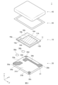
- the crystal oscillator 100 includes a crystal resonator 1, a mounting substrate 130, a cover 140, and electronic components 156.
- the quartz crystal unit 1 and electronic components 156 are housed in a space formed between the mounting substrate 130 and the lid 140.
- the space formed by the mounting substrate 130 and the lid 140 is, for example, hermetically sealed. This space may be hermetically sealed in a vacuum state, or may be hermetically sealed when filled with a gas such as an inert gas.
- the mounting board 130 is a flat circuit board.
- the mounting board 130 is configured to include, for example, a glass epoxy board and a wiring layer patterned on the glass epoxy board.
- the quartz crystal oscillator 1 is provided on one surface (the upper surface in FIG. 1) of the mounting substrate 130. More specifically, the quartz crystal oscillator 1 is electrically connected to the wiring layer of the mounting substrate 130 by solder 153.
- the lid 140 includes a bottomed opening that is open on one side (the lower side in FIG. 1).
- the lid 140 includes a flat top wall portion, a side wall portion that extends from the outer edge of the top wall portion toward the mounting substrate 130, and a flange portion that extends outward from the tip of the side wall portion.
- the flange portion is bonded to one surface of the mounting substrate 130 (the upper surface in FIG. 1). This allows the crystal unit 1 bonded to the mounting substrate 130 to be housed inside the lid 140.
- the lid 140 is made of a metal material and is formed, for example, by drawing a metal plate.
- the electronic component 156 is provided on one surface (the upper surface in FIG. 1 ) of the mounting board 130. More specifically, the wiring layer of the mounting board 130 and the electronic component 156 are joined by solder 153. In this way, the electronic component 156 is mounted on the mounting board 130.
- the electronic component 156 is electrically connected to the crystal oscillator 1 through the wiring layer of the mounting substrate 130.
- the electronic component 156 includes, for example, a capacitor and an IC chip.
- the electronic component 156 is, for example, part of an oscillation circuit that causes the crystal oscillator 1 to oscillate, or part of a temperature compensation circuit that compensates for the temperature characteristics of the crystal oscillator 1.
- the crystal oscillator 100 corresponds to an example of a temperature compensated crystal oscillator (TCXO: Temperature Compensated Crystal Oscillator).
- the crystal oscillator 100 may correspond to an example of a voltage controlled crystal oscillator (VCXO) or an example of an oven controlled crystal oscillator (OCXO).
- Figure 2 is an exploded perspective view of the quartz crystal resonator according to the first embodiment.
- Figure 3 is a cross-sectional view of the quartz crystal resonator according to the first embodiment.
- the Z'-axis direction corresponds to an example of a "first direction”
- the X-axis direction corresponds to an example of a "second direction”
- the Y'-axis direction corresponds to an example of a "third direction”.
- the Y'-axis direction corresponds to an example of a "thickness direction”.
- the first direction, second direction, and third direction are not limited to the above.
- the X-axis direction may be the first direction
- the Z'-axis direction may be the second direction.
- the quartz crystal oscillator 1 comprises a quartz crystal oscillator element 10, a base member 30, a cover member 40, and a joint portion 50.
- the quartz crystal element 10 is an electromechanical energy conversion element that converts electrical energy into mechanical energy and vice versa by the piezoelectric effect.
- the main mode frequency of the quartz crystal element 10 is, for example, about 0.8 GHz to about 2.0 GHz, for example, about 0.95 GHz.
- the inharmonic mode frequency of the quartz crystal element 10 is, for example, within a range of about 1% of the main mode frequency.
- the quartz crystal element 10 includes a thin quartz crystal piece (Quartz Crystal Element) 11, a first excitation electrode 14a and a second excitation electrode 14b that constitute a pair of excitation electrodes, a first extraction electrode 15a and a second extraction electrode 15b that constitute a pair of extraction electrodes, a first connection electrode 16a and a second connection electrode 16b that constitute a pair of connection electrodes, and a mass addition film 20.
- the quartz crystal piece 11 has an upper surface 11A and a lower surface 11B that face each other.
- the upper surface 11A is located on the side that faces the top wall portion 41 of the cover member 40.
- the lower surface 11B is located on the side that faces the base member 30.
- the upper surface 11A and the lower surface 11B correspond to a pair of main surfaces of the quartz crystal piece 11.
- the quartz piece 11 is, for example, an AT-cut quartz crystal.
- An AT-cut quartz crystal is formed so that the XZ' plane is the main surface and the thickness is in the direction parallel to the Y' axis.
- the shape of the quartz piece 11 (hereinafter referred to as the "planar shape") is a square having a pair of sides extending in the Z' axis direction and a pair of sides extending in the X axis direction.
- the quartz piece 11 also has a thickness in the Y' axis direction.
- the shape of the quartz piece 11 is a flat plate with a uniform thickness.
- the planar shape of the quartz piece is not limited to the above.
- the planar shape of the quartz piece may be a rectangle having a long side extending in the Z'-axis direction and a short side extending in the X-axis direction, or a rectangle having a short side extending in the Z'-axis direction and a long side extending in the X-axis direction.
- the planar shape of the quartz piece may be a polygon, a circle, an ellipse, or a combination of these.
- the quartz piece is not limited to being flat.
- the quartz piece may have a mesa structure or an inverted mesa structure with unevenness on at least one of the upper surface 11A and the lower surface 11B.
- the quartz piece may have a convex structure in which the amount of change in thickness changes continuously, or a bevel structure in which the amount of change in thickness changes discontinuously.
- the AT-cut quartz piece 11 is cut out with the XZ' plane as the main surface, with the Y' axis and Z' axis being the axes obtained by rotating the Y and Z axes around the X axis by 35 degrees 15 minutes ⁇ 1 minute 30 seconds from the Y axis in the direction of the Z axis, out of the X, Y, and Z axes that are the crystal axes of synthetic quartz crystal.
- the quartz crystal vibration element 10 using the AT-cut quartz crystal piece 11 has high frequency stability over a wide temperature range.
- the AT-cut quartz crystal vibration element has excellent aging characteristics and can be manufactured at low cost.
- the AT-cut quartz crystal vibration element uses the thickness shear vibration mode as the main vibration.
- the cut angle of the quartz crystal piece is not limited to the above.
- the rotation angle of the Y'-axis and Z'-axis in the AT-cut quartz crystal piece 11 may be tilted in the range of -5 degrees or more or +15 degrees or less from 35 degrees 15 minutes.
- the cut angle of the quartz crystal piece may be a different cut other than the AT cut, such as a BT cut, a GT cut, or an SC cut.
- the main vibration mode of the quartz crystal vibrating element is not limited to the thickness-shear vibration mode, and may be, for example, thickness-extensional vibration, splay vibration, length vibration, or bending vibration.
- the first excitation electrode 14a and the second excitation electrode 14b apply an alternating voltage to the crystal blank 11 to excite the crystal blank 11.
- the first excitation electrode 14a and the second excitation electrode 14b are provided in the center of the crystal blank 11 in a plan view.
- the first excitation electrode 14a is provided on the upper surface 11A
- the second excitation electrode 14b is provided on the lower surface 11B.
- the first excitation electrode 14a and the second excitation electrode 14b face each other in the Y'-axis direction, sandwiching the crystal blank 11 therebetween.
- the first excitation electrode 14a corresponds to an example of an "excitation electrode.”
- the planar shape of the first excitation electrode 14 is a rectangle with a short side extending in the Z'-axis direction and a long side extending in the X-axis direction.
- the first excitation electrode 14a also has a thickness in the Y'-axis direction.
- the second excitation electrode 14b has a similar shape.
- the planar shape of the first excitation electrode and the second excitation electrode is not limited to the above.
- the planar shape of the first excitation electrode and the second excitation electrode may be a rectangle having a short side extending in the X-axis direction.
- the planar shape of the first excitation electrode and the second excitation electrode may be a square, polygonal, circular, elliptical, or a combination of these.
- the first extraction electrode 15a electrically connects the first excitation electrode 14a and the first connection electrode 16a
- the second extraction electrode 15b electrically connects the second excitation electrode 14b and the second connection electrode 16b.
- the first extraction electrode 15a is provided across the upper surface 11A and the lower surface 11B of the crystal piece 11, and the second extraction electrode 15b is provided on the lower surface 11B of the crystal piece 11.
- the first connection electrode 16a and the second connection electrode 16b electrically connect the quartz crystal vibration element 10 to the base member 30.
- the first connection electrode 16a and the second connection electrode 16b are provided on the lower surface 11B of the quartz crystal piece 11.
- the first excitation electrode 14a, the first extraction electrode 15a, and the first connection electrode 16a are integrally provided.
- These electrodes of the quartz crystal vibration element 10 have a multi-layer structure in which, for example, a base layer and a surface layer are laminated in this order.
- the base layer is a chromium (Cr) layer that has good adhesion to the quartz crystal blank 11
- the surface layer is a gold (Au) layer that has good chemical stability.
- the electrodes of the quartz crystal vibration element 10 may contain titanium (Ti), aluminum (Al), molybdenum (Mo), or an aluminum-copper alloy (AlCu) mainly composed of aluminum (Al).
- the electrodes of the quartz crystal vibration element 10 may have a single-layer structure.
- the mass-adding film 20 reduces the sound velocity in a portion of the region where the first excitation electrode 14a and the second excitation electrode 14b face each other through the mass-adding effect.
- the mass-adding film 20 is provided on the side of the first excitation electrode 14a opposite the crystal blank 11. At least a portion of the mass-adding film 20 overlaps the first excitation electrode 14a.
- the material of the mass-adding film 20 is an electrical conductor, and is, for example, the same as the material of the first excitation electrode 14a.
- the mass-adding film may be provided on the opposite side of the second excitation electrode to the crystal piece 11, rather than on the opposite side of the first excitation electrode to the crystal piece.
- the material of the mass-adding film 20 may be a metal different from that of the first excitation electrode, or may be an insulator.
- the base member 30 holds the quartz crystal vibration element 10 so that it can vibrate.
- the base member 30 includes a substrate 31, connection electrodes 33a and 33b, extraction electrodes 34a and 34b, external electrodes 35a, 35b, 35c, and 35d, and conductive holding members 36a and 36b.
- the base 31 is a plate-shaped insulator having an upper surface 31A and a lower surface 31B that face each other in the thickness direction.
- the upper surface 31A and the lower surface 31B correspond to a pair of main surfaces of the base 31.
- the upper surface 31A is located on the side facing the quartz vibration element 10 and the lid member 40, and corresponds to the mounting surface on which the quartz vibration element 10 is mounted.
- the base 31 is preferably made of a heat-resistant material.
- the base 31 may be made of a material having a thermal expansion coefficient close to that of the quartz piece 11.
- the base 31 is made of, for example, a ceramic substrate, a glass substrate, or a quartz substrate.
- the corner portion of the base 31 has a cutout side surface formed in a cylindrical curved shape (also called a castellation shape). Note that the shape of the corner portion of the base 31 is not limited to this.
- the corner portion of the base may have a cutout side surface formed in a rectangular column shape, or may be a substantially right-angled corner portion without a cutout.
- connection electrodes 33a and 33b are electrically connected to the quartz crystal vibration element 10.
- the connection electrode 33a is electrically connected to the connection electrode 16a of the quartz crystal vibration element 10
- the connection electrode 33b is connected to the connection electrode 16b of the quartz crystal vibration element 10.
- the extraction electrode 34a electrically connects the connection electrode 33a to the external electrode 35a
- the extraction electrode 34b electrically connects the connection electrode 33b to the external electrode 35b.
- the extraction electrodes 34a and 34b are provided on the upper surface 31A of the base 31.
- the external electrodes 35a and 35b are external terminals for electrically connecting the quartz crystal vibration element 10 to an external substrate.
- the external electrode 35a electrically connects the first excitation electrode 14a of the quartz crystal vibration element 10 to the mounting substrate 130
- the external electrode 35b electrically connects the second excitation electrode 14b of the quartz crystal vibration element 10 to the mounting substrate 130.
- One of the external electrodes 35c and 35d is a ground electrode that grounds the cover member 40, and the other is a dummy electrode that is not electrically connected to the quartz crystal vibration element 10 and the cover member 40.
- Each of the external electrodes 35a, 35b, 35c, and 35d is continuously provided from the cutout side surface provided at the four corners of the base 31 to the lower surface 31B. In the example shown in FIG.
- the external electrodes 35a and 35b are located at diagonal corners on the upper surface 31A of the base 31, and the external electrodes 35c and 35d are located at different diagonal corners on the upper surface 31A of the base 31.
- the external electrodes 35a, 35b, 35c, and 35d are not limited to the above. Both the external electrodes 35c and 35d may be ground electrodes, or both may be dummy electrodes. The external electrodes 35c and 35d may be omitted.
- the external electrode 35c may be electrically connected to one of the external electrodes 35a and 35b, and the external electrode 35d may be electrically connected to the other of the external electrodes 35a and 35b.
- the conductive holding members 36a and 36b electrically connect the base member 30 and the quartz vibration element 10, and mechanically hold the quartz vibration element 10.
- the conductive holding member 36a electrically connects the first connection electrode 16a of the quartz vibration element 10 to the connection electrode 33a of the base member 30.
- the conductive holding member 36b electrically connects the second connection electrode 16b of the quartz vibration element 10 to the connection electrode 33b of the base member 30.
- the conductive holding members 36a and 36b are hardened conductive adhesives containing thermosetting resins, photocurable resins, etc.
- the main component of the conductive holding members 36a and 36b is, for example, silicone resin.
- the conductive holding members 36a and 36b contain conductive particles, and the conductive particles are, for example, metal particles containing silver (Ag).
- the main component of the conductive holding members 36a, 36b is not limited to silicone resin, but may be, for example, epoxy resin or acrylic resin.
- the conductive particles contained in the conductive holding members 36a, 36b are not limited to silver particles, but may be formed from other metals, conductive ceramics, conductive organic materials, etc.
- the conductive holding members 36a, 36b may contain a conductive polymer.
- the cover member 40 has a top wall portion 41, a side wall portion 42 extending from the outer edge of the top wall portion 41 toward the base member 30, and a flange portion 43 extending outward from the tip of the mounting substrate 130.
- the top wall portion 41 faces the base member 30 in the Y'-axis direction, sandwiching the crystal vibration element 10 therebetween.
- the side wall portion 42 surrounds the crystal vibration element 10 at a distance in the XZ'-plane direction.
- the flange portion 43 is provided in a frame shape in a plan view, and is provided closest to the base member 30 among the cover member 40.
- the material of the cover member 40 is preferably a conductive material, and more preferably a metal material with high airtightness. By making the cover member 40 out of a conductive material, an electromagnetic shielding function that reduces the entry and exit of electromagnetic waves into the internal space 39 is imparted to the cover member 40. From the viewpoint of suppressing the occurrence of thermal stress, it is desirable that the material of the lid member 40 has a thermal expansion coefficient close to that of the base member 30, for example, an Fe-Ni-Co alloy whose thermal expansion coefficient at room temperature matches that of glass or ceramic over a wide temperature range.
- the lid member 40 is electrically connected to at least one of the external electrodes 35c, 35d by a grounding member (not shown).
- the joint 50 joins the base member 30 and the lid member 40 and seals the internal space 39.
- the joint 50 is provided in a frame shape around the entire circumference of the flange portion 43 of the base member 30 and is sandwiched between the lower surface of the flange portion 43 of the lid member 40 and the upper surface 31A of the base member 30.
- the joint 50 is provided by an insulating material.
- the joint 50 is provided by an organic adhesive containing, for example, an epoxy-based, vinyl-based, acrylic-based, urethane-based, or silicone-based resin.
- the material of the joint 50 is not limited to organic adhesives, and may be inorganic adhesives such as silicon-based adhesives containing water glass, calcium-based adhesives containing cement, etc.
- the material of the joint 50 may be low-melting point glass (for example, lead borate-based or tin phosphate-based).
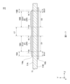
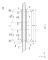
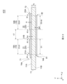
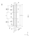
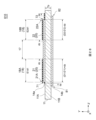
- FIG. 4 is a cross-sectional view of the quartz crystal vibration element according to the first embodiment.
- Figure 5 is a plan view of the quartz crystal vibration element according to the first embodiment. Note that, to simplify the description, the first extraction electrode 15a, the second extraction electrode 15b, the first connection electrode 16a, and the second connection electrode 16b are omitted from illustration in Figures 4 and 5.
- the high acoustic velocity region 17 is provided in a region that overlaps with the center of the first excitation electrode 14a.
- the planar shape of the high acoustic velocity region 17 is a rectangle having a long side extending along the X-axis direction and a short side extending along the Z'-axis direction.
- the low acoustic velocity region 18 is provided along the outer edge of the first excitation electrode 14a in the region inside the outer edge of the first excitation electrode 14a.
- the low acoustic velocity region 18 is provided in a frame shape surrounding the center of the first excitation electrode 14a.
- the low acoustic velocity region 18 has a first low acoustic velocity region 18A, a second low acoustic velocity region 18B, a third low acoustic velocity region 18C, and a fourth low acoustic velocity region 18D.
- the first low sound speed region 18A is adjacent to the high sound speed region 17 on the negative side of the Z' axis and extends along the X-axis direction.
- the second low sound speed region 18B is adjacent to the high sound speed region 17 on the positive side of the Z' axis and extends along the X-axis direction.
- the third low sound speed region 18C is adjacent to the high sound speed region 17 on the positive side of the X-axis and extends along the Z' axis.
- the fourth low sound speed region 18D is adjacent to the high sound speed region 17 on the negative side of the X-axis and extends along the Z' axis.
- the end of the first low sound speed region 18A on the positive side of the X-axis is connected to the end of the third low sound speed region 18C on the negative side of the Z' axis, and the end of the first low sound speed region 18A on the positive side of the X-axis is connected to the end of the fourth low sound speed region 18D on the negative side of the Z' axis.
- the end of the second low sound speed region 18B on the positive side of the X-axis is connected to the end of the third low sound speed region 18C on the positive side of the Z'-axis, and the end of the second low sound speed region 18B on the negative side of the X-axis is connected to the end of the fourth low sound speed region 18D on the positive side of the Z'-axis.
- the end of the first low sound speed region 18A on the positive X-axis side overlaps with the end of the third low sound speed region 18C on the negative Z'-axis side
- the end of the first low sound speed region 18A on the negative X-axis side overlaps with the end of the fourth low sound speed region 18D on the negative Z'-axis side
- the end of the second low sound speed region 18B on the positive X-axis side overlaps with the end of the third low sound speed region 18C on the positive Z'-axis side
- the end of the second low sound speed region 18B on the negative X-axis side overlaps with the end of the fourth low sound speed region 18D on the positive Z'-axis side.
- the outer edge portion located on the opposite side to the center of the first excitation electrode 14a in the first low acoustic velocity region 18A overlaps with the outer edge portion (outer edge portion 21A described later) located on the opposite side to the center of the first excitation electrode 14a in the first part 21 described later of the mass addition film 20.
- the outer edge portion located on the opposite side to the center of the first excitation electrode 14a in the second low acoustic velocity region 18B overlaps with the outer edge portion (outer edge portion 22A described later) located on the opposite side to the center of the first excitation electrode 14a in the second part 22 described later of the mass addition film 20.
- the outer edge portion located on the opposite side to the center of the first excitation electrode 14a in the third low acoustic velocity region 18C overlaps with the outer edge portion (outer edge portion 23A described later) located on the opposite side to the center of the first excitation electrode 14a in the third part 23 described later of the mass addition film 20.
- the outer edge portion located on the opposite side to the center of the first excitation electrode 14a in the fourth low sound velocity region 18D overlaps with the outer edge portion (outer edge portion 24A described later) located on the opposite side to the center of the first excitation electrode 14a in the fourth portion 24 described later of the mass addition film 20.
- the inner edge portion located on the central side of the first excitation electrode 14a in the first low acoustic velocity region 18A overlaps with the inner edge portion (inner edge portion 21B described later) located on the central side of the first excitation electrode 14a in the first part 21 of the mass addition film 20 described later.
- the inner edge portion located on the central side of the first excitation electrode 14a in the second low acoustic velocity region 18B overlaps with the inner edge portion (inner edge portion 22B described later) located on the central side of the first excitation electrode 14a in the second part 22 of the mass addition film 20 described later.
- both the outer edge portion 71 of the first excitation electrode 14a, which will be described later, and the outer edge portion 81 of the second excitation electrode 14b, which will be described later, are further away from the center of the first excitation electrode 14a than the outer edge portion of the first low sonic velocity region 18A.
- the outer edge portion 81 is further away from the center of the first excitation electrode 14a than the outer edge portion 71.
- Both the outer edge portion 72 of the first excitation electrode 14a, which will be described later, and the outer edge portion 82 of the second excitation electrode 14b, which will be described later, are further away from the center of the first excitation electrode 14a than the outer edge portion of the second low sonic velocity region 18B.
- Both the outer edge portion 74 of the first excitation electrode 14a, which will be described later, and the outer edge portion 84 of the second excitation electrode 14b, which will be described later, are farther from the center of the first excitation electrode 14a than the outer edge portion of the fourth low sound velocity region 18D.
- the outer edge portion 84 is farther from the center of the first excitation electrode 14a than the outer edge portion 73.
- the shape of the low sound velocity region is not limited to the above.
- the third low sound velocity region and the fourth low sound velocity region may be omitted. That is, the high sound velocity region, the first low sound velocity region, and the second low sound velocity region may be arranged in a band shape extending parallel to each other along the X-axis direction. Also, the first low sound velocity region and the second low sound velocity region may be omitted, and the high sound velocity region, the third low sound velocity region, and the fourth low sound velocity region may be arranged in a band shape extending parallel to each other along the Z'-axis direction.
- the end of the first low sound velocity region on the positive side of the X-axis may be separated from the third low sound velocity region, and the end of the first low sound velocity region on the negative side of the X-axis may be separated from the fourth low sound velocity region.
- the end of the second low sound velocity region on the positive side of the X-axis may be separated from the third low sound velocity region, and the end of the second low sound velocity region on the negative side of the X-axis may be separated from the fourth low sound velocity region.
- the first low sound velocity region may be adjacent to the high sound velocity region on the positive side of the Z' axis
- the second low sound velocity region may be adjacent to the high sound velocity region on the negative side of the Z' axis.
- the third low sound velocity region may be adjacent to the high sound velocity region on the negative side of the X axis
- the fourth low sound velocity region may be adjacent to the high sound velocity region on the positive side of the X axis.
- the outer high acoustic velocity region 19 is provided along the outer edge of the first excitation electrode 14a in the region between the outer edge of the mass-adding film 20 and the outer edge of the first excitation electrode 14a.
- the outer high acoustic velocity region 19 is provided in a frame shape surrounding the low acoustic velocity region 18.
- the outer high acoustic velocity region 19 has a first outer high acoustic velocity region 19A, a second outer high acoustic velocity region 19B, a third outer high acoustic velocity region 19C, and a fourth outer high acoustic velocity region 19D.
- the first outer high sound velocity region 19A is adjacent to the negative side of the Z' axis of the first low sound velocity region 18A and extends along the X-axis direction.
- the second outer high sound velocity region 19B is adjacent to the positive side of the Z' axis of the second low sound velocity region 18B and extends along the X-axis direction.
- the third outer high sound velocity region 19C is adjacent to the positive side of the X-axis of the third low sound velocity region 18C and extends along the Z' axis direction.
- the fourth outer high sound velocity region 19D is adjacent to the negative side of the X-axis of the fourth low sound velocity region 18D and extends along the Z' axis direction.
- the end of the first outer high sound velocity region 19A on the positive side of the X-axis is connected to the end of the third outer high sound velocity region 19C on the negative side of the Z' axis, and the end of the first outer high sound velocity region 19A on the negative side of the X-axis is connected to the end of the fourth outer high sound velocity region 19D on the negative side of the Z' axis.
- the end of the second outer high sound velocity region 19B on the positive side of the X-axis is connected to the end of the third outer high sound velocity region 19C on the positive side of the Z'-axis, and the end of the second outer high sound velocity region 19B on the negative side of the X-axis is connected to the end of the fourth outer high sound velocity region 19D on the positive side of the Z'-axis.
- the end of the first outer high sound velocity region 19A on the positive X-axis side overlaps with the end of the third outer high sound velocity region 19C on the negative Z'-axis side, and the end of the first outer high sound velocity region 19A on the negative X-axis side overlaps with the end of the fourth outer high sound velocity region 19D on the negative Z'-axis side.
- the end of the second outer high sound velocity region 19B on the positive X-axis side overlaps with the end of the third outer high sound velocity region 19C on the positive Z'-axis side, and the end of the second outer high sound velocity region 19B on the negative X-axis side overlaps with the end of the fourth outer high sound velocity region 19D on the positive Z'-axis side.
- the shape of the outer high sound velocity region is not limited to the above.
- the third outer high sound velocity region and the fourth outer high sound velocity region may be omitted. That is, the first outer high sound velocity region and the second outer high sound velocity region may be provided in a band shape extending parallel to each other along the X-axis direction. In this case, the first outer high sound velocity region and the second outer high sound velocity region may be provided from the end of the first excitation electrode on the negative side of the X-axis to the end on the positive side of the X-axis in a planar view.
- first outer high sound velocity region and the second outer high sound velocity region may be omitted, and the third outer high sound velocity region and the fourth outer high sound velocity region may be provided in a band shape extending parallel to each other along the Z'-axis direction.
- the third outer high sound velocity region and the fourth outer high sound velocity region may be provided from the end of the first excitation electrode on the negative side of the Z'-axis to the end on the positive side of the Z'-axis in a planar view.
- the first outer high sound velocity region may be spaced apart from the third outer high sound velocity region and may be spaced apart from the fourth outer high sound velocity region.
- the second outer high sound velocity region may be spaced apart from the third outer high sound velocity region and may be spaced apart from the fourth outer high sound velocity region.
- the high sound velocity region 17, the low sound velocity region 18, and the outer high sound velocity region 19 are provided with a quartz crystal piece 11, a first excitation electrode 14a, and a second excitation electrode 14b.
- the low sound velocity region 18 is further provided with a mass addition film 20.
- the mass addition film 20 is provided so as to avoid the high sound velocity region 17 and the outer high sound velocity region 19.
- the planar shape of the mass addition film 20 is a frame shape that overlaps with the low sound velocity region 18.
- the first excitation electrode 14a has outer edges 71, 72, 73, and 74.
- Outer edge 71 is the edge of one side that extends along the X-axis on the negative Z'-axis side among the four edges of the first excitation electrode 14a when viewed in a plane.
- Outer edge 72 is the edge of one side that extends along the X-axis on the positive Z'-axis side
- outer edge 73 is the edge of one side that extends along the Z'-axis on the positive X-axis side
- outer edge 74 is the edge of one side that extends along the Z'-axis on the negative X-axis side.
- the second excitation electrode 14b has outer edges 81, 82, 83, and 84.
- Outer edge 81 is the edge of one side that extends along the X-axis on the negative Z'-axis side among the four edges of the first excitation electrode 14a when viewed in a plane.
- Outer edge 82 is the edge of one side that extends along the X-axis on the positive Z'-axis side
- outer edge 83 is the edge of one side that extends along the Z'-axis on the positive X-axis side
- outer edge 84 is the edge of one side that extends along the Z'-axis on the negative X-axis side.
- the fourth portion 24 is provided along the outer edge 74 of the first excitation electrode 14a located on the negative side of the X-axis, avoiding the high acoustic velocity region 17.
- the first portion 21 is spaced apart from the outer edge 71
- the second portion 22 is spaced apart from the outer edge 72
- the third portion 23 is spaced apart from the outer edge 73
- the fourth portion 24 is spaced apart from the outer edge 74.
- the first portion 21 has an outer edge 21A located on the side of the outer high sound velocity region 19 and an inner edge 21B located on the side of the high sound velocity region 17.
- the second portion 22 has an outer edge 22A located on the side of the outer high sound velocity region 19 and an inner edge 22B located on the side of the high sound velocity region 17.
- the third portion 23 has an outer edge 23A located on the side of the outer high sound velocity region 19 and an inner edge 23B located on the side of the high sound velocity region 17.
- the fourth portion 24 has an outer edge 24A located on the side of the outer high sound velocity region 19 and an inner edge 24B located on the side of the high sound velocity region 17.
- Outer edge portions 21A, 22A, 23A, and 24A are located at the boundary between low sound velocity region 18 and outer high sound velocity region 19.
- Inner edge portions 21B, 22B, 23B, and 24B are located at the boundary between high sound velocity region 17 and low sound velocity region 18.
- the end portion on the positive X-axis side of outer edge portion 21A is connected to the end portion on the negative Z'-axis side of outer edge portion 23A, and the end portion on the negative X-axis side of outer edge portion 21A is connected to the end portion on the negative Z'-axis side of outer edge portion 24A.
- the end of inner edge 22B on the positive X-axis side is connected to the end of inner edge 23B on the positive Z'-axis side, and the end of inner edge 22B on the negative X-axis side is connected to the end of inner edge 24B on the positive Z'-axis side.
- the outer edge portions 71 and 72 of the first excitation electrode 14a overlap the second excitation electrode 14b.
- the outer edge portions 71 and 72 of the first excitation electrode 14a are located between the outer edge portions 81 and 82 of the second excitation electrode 14b.
- the outer edge portion 71 of the first excitation electrode 14a is located between the outer edge portion 81 of the second excitation electrode 14b and the outer edge portion 21A of the first part 21 of the mass addition film 20.
- the outer edge portion 72 of the first excitation electrode 14a is located between the outer edge portion 82 of the second excitation electrode 14b and the outer edge portion 22A of the second part 22 of the mass addition film 20.
- the outer edge portions 73 and 74 of the first excitation electrode 14a overlap the second excitation electrode 14b.
- the outer edges 73 and 74 of the first excitation electrode 14a are located between the outer edges 83 and 84 of the second excitation electrode 14b.
- the outer edge 73 of the first excitation electrode 14a is located between the outer edge 83 of the second excitation electrode 14b and the outer edge 23A of the third portion 23 of the mass addition film 20.
- the outer edge 74 of the first excitation electrode 14a is located between the outer edge 84 of the second excitation electrode 14b and the outer edge 24A of the fourth portion 24 of the mass addition film 20.
- the distance along the Z'-axis direction between the outer edge 21A of the first part 21 of the mass addition film 20 and the outer edge 22A of the second part 22 is defined as length A.
- the distance along the Z'-axis direction between the inner edge 21B of the first part 21 of the mass addition film 20 and the inner edge 22B of the second part 22 is defined as length A'.
- the distance along the Z'-axis direction between the outer edge 71 and the outer edge 72 of the first excitation electrode 14a is defined as length B.
- the distance along the Z'-axis direction between the outer edge 21A of the first part 21 of the mass addition film 20 and the outer edge 71 of the first excitation electrode 14a is defined as length B1.
- the distance along the Z'-axis direction between the outer edge 22A of the second part 22 of the mass addition film 20 and the outer edge 72 of the first excitation electrode 14a is defined as length B2.
- the distance along the Z'-axis direction between the outer edge 81 and the outer edge 82 of the second excitation electrode 14b is defined as length C.
- the distance along the Z'-axis direction between the outer edge 71 of the first excitation electrode 14a and the outer edge 81 of the second excitation electrode 14b is defined as length C1.
- the distance along the Z'-axis direction between the outer edge 72 of the first excitation electrode 14a and the outer edge 82 of the second excitation electrode 14b is defined as length C2.
- the distance along the Z'-axis direction between the outer edge 21A and the inner edge 21B of the first part 21 of the mass addition film 20 is defined as length D1
- the distance along the Z'-axis direction between the outer edge 22A and the inner edge 22B of the second part 22 of the mass addition film 20 is defined as length D2.
- the distance along the Z'-axis direction between the outer edge of the first low sound velocity region 18A on the opposite side to the second low sound velocity region 18B and the outer edge of the second low sound velocity region 18B on the opposite side to the first low sound velocity region 18A is defined as length E.
- the distance along the Z'-axis direction between the outer edge of the first low sonic speed region 18A on the opposite side to the second low sonic speed region 18B and the outer edge of the second low sonic speed region 18B side is defined as length E1.
- the distance along the Z'-axis direction between the outer edge of the second low sonic speed region 18B on the opposite side to the first low sonic speed region 18A and the outer edge of the first low sonic speed region 18A side is defined as length E2.
- Length A corresponds to the dimension of the mass-added film 20 along the Z'-axis direction.
- Length A' corresponds to the dimension of the high acoustic velocity region 17 along the Z'-axis direction.
- Length B corresponds to the dimension of the first excitation electrode 14a along the Z'-axis direction, and corresponds to the sum of the dimensions of the high acoustic velocity region 17, the first low acoustic velocity region 18A, the second low acoustic velocity region 18B, the first outer high acoustic velocity region 19A, and the second outer high acoustic velocity region 19B along the Z'-axis direction.
- Length B1 corresponds to the dimension of the first outer high acoustic velocity region 19A along the Z'-axis direction
- length B2 corresponds to the dimension of the second outer high acoustic velocity region 19B along the Z'-axis direction
- Length C corresponds to the dimension of the second excitation electrode 14b along the Z'-axis direction
- Length C1 corresponds to the dimension of the portion of the second excitation electrode 14b extending from the first excitation electrode 14a to the negative Z'-axis direction in a plan view along the Z'-axis direction.
- the length C2 corresponds to the dimension along the Z'-axis direction of the portion of the second excitation electrode 14b that extends from the first excitation electrode 14a toward the positive side of the Z'-axis direction in a plan view.
- the length D1 corresponds to the dimension along the Z'-axis direction of the first portion 21 of the mass addition film 20, and the length D2 corresponds to the dimension along the Z'-axis direction of the second portion 22 of the mass addition film 20.
- the length E corresponds to the sum of the dimensions along the Z'-axis direction of the high sound velocity region 17 and the low sound velocity region 18.
- the length E' corresponds to the dimension along the Z'-axis direction of the high sound velocity region 17.
- the length E1 corresponds to the dimension along the Z'-axis direction of the first low sound velocity region 18A.
- the length E2 corresponds to the dimension along the Z'-axis direction of the second low sound velocity region 18B.
- the length A is determined by measuring the distance in the Z'-axis direction between the outer edges 21A and 22A.
- the length A' is determined by measuring the distance in the Z'-axis direction between the inner edges 21B and 22B.
- the length B is determined by measuring the distance in the Z'-axis direction between the outer edges 71 and 72.
- the length B1 is determined by measuring the distance in the Z'-axis direction between the outer edges 21A and 71
- the length B2 is determined by measuring the distance in the Z'-axis direction between the outer edges 22A and 72.
- the length C is determined by measuring the distance in the Z'-axis direction between the outer edges 81 and 82.
- the length C1 is determined by measuring the distance in the Z'-axis direction between the outer edges 71 and 81
- the length C2 is determined by measuring the distance in the Z'-axis direction between the outer edges 72 and 82.
- the length D1 is determined by measuring the distance in the Z'-axis direction between the outer edge portion 21A and the inner edge portion 21B
- the length D2 is determined by measuring the distance in the Z'-axis direction between the outer edge portion 22A and the inner edge portion 22B.
- the length E is determined by measuring the distance in the Z'-axis direction between the outer edge portion 21A and the outer edge portion 22A. Also, the length E' is determined by measuring the distance in the Z'-axis direction between the inner edge portion 21B and the inner edge portion 22B, the length E1 is determined by measuring the distance in the Z'-axis direction between the outer edge portion 21A and the inner edge portion 21B, and the length E2 is determined by measuring the distance in the Z'-axis direction between the outer edge portion 22A and the inner edge portion 22B.
- the length A is determined by a method other than the above.
- the length A may be determined as the maximum value of the distance between the outer edges 21A and 22A.
- the length A may be determined as the average or minimum value of the distance between the outer edges 21A and 22A.
- the length A may also be determined by dividing the area of the region surrounded by the outer edges 21A, 22A, 23A, and 24A of the mass-adding film 20 by the distance in the X-axis direction between the outer edges 23A and 24A.
- the length A may also be determined by measuring the distance between the outer edges 21A and 22A on the inner edges 23B of the mass-adding film 20 or on a tangent line that is in contact with the inner edges 23B and extends in the Z'-axis direction in planar view. Lengths A', B, B1, B2, C, C1, C2, D1, D2, E, E', E1, and E2 may also be specified in the same manner as length A.
- length A is smaller than length B
- length B is smaller than length C (A ⁇ B ⁇ C).
- length C1 is larger than length B1 (B1 ⁇ C1)
- length C2 is larger than length B2 (B2 ⁇ C2).
- length D1 is equal to or greater than length A' (A' ⁇ D1)
- length D2 is equal to or greater than length A' (A' ⁇ D2).
- the ratio A'/B of length A' to length B is, for example, equal to or greater than 0.02 (0.02 ⁇ A'/B).
- the relationship 0.05 ⁇ A'/B ⁇ 0.5 holds. More preferably, the relationship 0.20 ⁇ A'/B ⁇ 0.47 holds.
- the magnitude relationship between the lengths A, A', B, B1, B2, C, C1, C2, D1, and D2 is not limited to the above.
- the relationship B1 ⁇ B2 or B2 ⁇ B1 may hold, or the relationship C1 ⁇ C2 or C2 ⁇ C1 may hold.
- the relationship C1 ⁇ B1 may hold, or the relationship C2 ⁇ B2 may hold.
- the relationship D1 ⁇ D2 or D2 ⁇ D1 may hold.
- the relationship D1 ⁇ A' may hold, or the relationship D2 ⁇ A' may hold.
- the thickness of the crystal blank 11 is Tp
- the thickness of the first excitation electrode 14a is Te1
- the thickness of the second excitation electrode 14b is Te2
- the thickness of the mass addition film 20 is Tf.
- the thickness Tf of the mass addition film 20 may be specified as the distance along the Y'-axis direction between the surface of the first excitation electrode 14a in the high sound velocity region 17 and the surface of the mass addition film 20 in the low sound velocity region 18.
- the thickness Tf of the mass addition film 20 may also be specified as the height of the step at the outer edge portions 21A, 22A, 23A, and 24A of the mass addition film 20, or as the height of the step at the inner edge portions 21B, 22B, 23B, and 24B of the mass addition film 20. However, if the height of the steps at the outer edges 21A, 22A, 23A, and 24A is different from the height of the steps at the inner edges 21B, 22B, 23B, and 24B, the thickness Tf of the mass-adding film 20 is specified as the height of the steps at the inner edges 21B, 22B, 23B, and 24B.
- the thickness Tp is approximately constant throughout the high sound velocity region 17, the low sound velocity region 18, and the outer high sound velocity region 19.
- the thicknesses Te1 and Te2 are approximately constant throughout the high sound velocity region 17, the low sound velocity region 18, and the outer high sound velocity region 19.
- the thickness Tf is approximately constant throughout the entire low sound velocity region 18.
- the first portion 21, the second portion 22, the third portion 23, and the fourth portion 24 are approximately equal in thickness.
- the thicknesses Te1 and Te2 are approximately 0.05 ⁇ m, and the thickness Tf is approximately 0.02 ⁇ m.
- thickness Tf may be equal to or greater than thickness Te1 (Te1 ⁇ Tf).
- Thickness Te1 may be smaller than thickness Te2 (Te1 ⁇ Te2), and thickness Te1 may be larger than thickness Te2 (Te2 ⁇ Te1).
- the dimension of the crystal blank 11 along the X-axis direction is defined as length Px
- the dimension of the crystal blank 11 along the Z'-axis direction is defined as length Pz.
- the dimension of the first excitation electrode 14a along the X-axis direction is defined as length Xe1
- the dimension of the first excitation electrode 14a along the Z'-axis direction is defined as length Ze1.
- the dimension of the second excitation electrode 14b along the X-axis direction is defined as length Xe2
- the dimension of the second excitation electrode 14b along the Z'-axis direction is defined as length Ze2.
- the distance along the Z'-axis direction between the outer edge 21A of the first part 21 of the mass addition film 20 and the outer edge 71 of the first excitation electrode 14a is defined as length Wgz.
- the distance along the Z'-axis direction between the outer edge 22A of the second part 22 of the mass addition film 20 and the outer edge 72 of the first excitation electrode 14a is defined as length Wgz.
- the distance along the Z'-axis direction between the inner edge 21B of the first portion 21 of the mass addition film 20 and the outer edge 71 of the first excitation electrode 14a is defined as the length Wz.
- the distance along the Z'-axis direction between the inner edge 22B of the second portion 22 of the mass addition film 20 and the outer edge 72 of the first excitation electrode 14a is defined as the length Wz.
- the distance along the X-axis direction between the outer edge 23A of the third portion 23 of the mass addition film 20 and the outer edge 73 of the first excitation electrode 14a is defined as the length Wgx.
- the distance along the X-axis direction between the outer edge 24A of the fourth portion 24 of the mass addition film 20 and the outer edge 74 of the first excitation electrode 14a is defined as the length Wgx.
- the distance along the X-axis direction between the inner edge 23B of the third portion 23 of the mass addition film 20 and the outer edge 73 of the first excitation electrode 14a is defined as the length Wx.
- the distance along the X-axis direction between the inner edge 24B of the fourth portion 24 of the mass addition film 20 and the outer edge 74 of the first excitation electrode 14a is defined as length Wx.
- the distance along the Z'-axis direction between the first portion 21 and the second portion 22 of the mass addition film 20 is defined as length Zf
- the distance along the X-axis direction between the third portion 23 and the fourth portion 24 of the mass addition film 20 is defined as length Xf.
- the dimension of the mass addition film 20 along the Z' axis direction can be expressed as 2 x Wz + Zf - 2 x Wgz, which is less than or equal to dimension Ze2 along the Z' axis direction of the second excitation electrode 14b (2 x Wz + Zf - 2 x Wgz ⁇ Ze2).
- the dimension of the mass addition film 20 along the X-axis direction can be expressed as 2 ⁇ Wx+Xf-2 ⁇ Wgx, which is equal to or smaller than the dimension Xe2 along the X-axis direction of the second excitation electrode 14b (2 ⁇ Wx+Xf-2 ⁇ Wgx ⁇ Xe2).
- Fig. 6 is a table showing the conditions of the simulation based on the first embodiment.
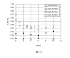
- Figs. 7 to 16 are graphs showing the simulation results based on the first embodiment.
- Figure 7 shows the simulation results based on the first embodiment.
- k_S0 is about 6.8%.
- FIG. 8 shows the simulation results based on the first embodiment.
- FIG. 9 shows the simulation results based on the second embodiment.
- the vertical axis shows the electromechanical coupling coefficient k (hereinafter also referred to as "k_A0") of the spurious A0 mode
- the simulation results of k_A0Z in a configuration in which there is no misalignment of the mass addition film 20 and the second excitation electrode 14b, and the simulation results of k_A0Z in a configuration in which there is a misalignment are plotted.
- k_A0Z in the configuration with misalignment is approximately equal to k_A0Z in the configuration without misalignment.
- the increase in k_A0Z is suppressed regardless of the dimensions and misalignment of the first excitation electrode 14a, the second excitation electrode 14b, and the mass addition film 20.
- FIG. 10 shows the simulation results based on the first embodiment.
- the vertical axis shows the Q value
- the graph plots the simulation results of the Q value in a configuration without misalignment of the mass addition film 20 and the second excitation electrode 14b, and the simulation results of the Q value in a configuration with misalignment.
- the direction and amount of misalignment in the configuration with misalignment in FIG. 10 are the same as the direction and amount of misalignment in the configuration with misalignment in FIG. 8 and FIG. 9.
- FIG. 11 shows the simulation results based on the first' embodiment.
- the graph plots the simulation results of k_S0 in a configuration where there is no misalignment of the mass addition film 20 and the second excitation electrode 14b, and the simulation results of k_S0 in a configuration where there is a misalignment.
- the direction and amount of misalignment in the configuration with misalignment in FIG. 11 is the same as the direction and amount of misalignment in the configuration with misalignment in FIG. 8 and FIG. 9.
- k_S0 does not change substantially in the range of 0 ⁇ x ⁇ 10 ⁇ m. Also, in the range of 0 ⁇ x ⁇ 10 ⁇ m, k_S0 in a configuration with misalignment is substantially equal to k_S0 in a configuration without misalignment. In other words, k_S0 is substantially constant regardless of the magnitude of x and the presence or absence of misalignment.
- FIG. 12 shows the simulation results based on the first' embodiment
- FIG. 13 shows the simulation results based on the second' embodiment
- FIG. 14 shows the simulation results based on the third' embodiment.
- the vertical axis indicates k_A0
- the graphs in FIGS. 12 to 14 plot the simulation results of k_A0X and k_A0Z in a configuration in which there is no misalignment of the mass addition film 20 and the second excitation electrode 14b, and the simulation results of k_A0X and k_A0Z in a configuration in which there is a misalignment.
- the direction and amount of misalignment in the configuration with misalignment in FIGS. 12 to 14 is the same as the direction and amount of misalignment in the configuration with misalignment in FIGS. 8 and 9.
- both k_A0X and k_A0Z are sufficiently reduced and are substantially constant in the range of 3 ⁇ m ⁇ x ⁇ 10 ⁇ m.
- the excitation suppression effect of the A0 mode is stable in the range of 3 ⁇ m ⁇ x ⁇ 10 ⁇ m.
- k_A0X and k_A0Z in the configuration with misalignment are substantially equal to k_A0X and k_A0Z in the configuration without misalignment.
- k_A0X and k_A0Z are substantially constant regardless of the size of x and the presence or absence of misalignment.
- k_A0X and k_A0Z show the same tendency. In other words, the increase in k_A0 is suppressed regardless of the dimensions and misalignment of the first excitation electrode 14a, the second excitation electrode 14b, and the mass addition film 20.
- FIG. 15 and 16 show the simulation results based on the first' embodiment.
- the vertical axis indicates the Q value
- the simulation results of the Q value in a configuration without misalignment of the mass addition film 20 and the second excitation electrode 14b, and the simulation results of the Q value in a configuration with misalignment are plotted.
- the direction and amount of misalignment in the configuration with misalignment in Fig. 15 are the same as the direction and amount of misalignment in the configuration with misalignment in Fig. 8 and Fig. 9.
- the Q value in the configuration with misalignment shows a similar trend to the Q value in the configuration without misalignment, and is approximately equal to the Q value in the configuration without misalignment. In other words, in the range of 0 ⁇ x ⁇ 8 ⁇ m, the decrease in the Q value is suppressed regardless of the presence or absence of misalignment.
- the Q value shows a similar tendency.
- the decrease in the Q value is suppressed regardless of the dimensions of the first excitation electrode 14a, the second excitation electrode 14b, and the mass addition film 20.
- Figure 17 is a diagram for explaining the effect of misalignment in the first embodiment.
- Figure 18 is a diagram for explaining the effect of misalignment in the first embodiment.
- Figure 17 is a cross-sectional view of the quartz crystal vibration element 10 when the mass addition film 20 is misaligned by dz in the positive direction of the Z' axis.
- Figure 18 is a cross-sectional view of the quartz crystal vibration element 10 when the second excitation electrode 14b is misaligned by dz in the negative direction of the Z' axis.
- the second portion 22 of the mass-adding film 20 extends from the first excitation electrode 14a toward the positive side of the Z'-axis in plan view.
- the balance of the lengths of the first low sound velocity region 18A and the second low sound velocity region 18B along the Z'-axis direction changes.
- the positional deviation on the same surface is, for example, a maximum of about 0.3 ⁇ m, so it is desirable to satisfy 0.5 ⁇ m ⁇ B', more desirably 1 ⁇ m ⁇ B', and even more desirably 2 ⁇ m ⁇ B'.
- the second excitation electrode 14b extends from the first excitation electrode 14a in the positive direction of the Z' axis in a plan view.
- the first excitation electrode 14a has a portion that does not overlap with the second excitation electrode 14b, and the balance of the lengths of the first outer high sound velocity region 19A and the second outer high sound velocity region 19B along the Z' axis direction changes.
- the positional deviation between different surfaces is, for example, a maximum of about 0.7 ⁇ m, so it is desirable to satisfy 1 ⁇ m ⁇ C', more desirably 2 ⁇ m ⁇ C', and even more desirably 4 ⁇ m ⁇ C'.
- the mass-adding film 20 is provided on the first excitation electrode 14a.
- the mass-adding film 20 is provided along the outer edge of the first excitation electrode 14a, and when the dimension of the mass-adding film 20 along the Z'-axis direction is A and the dimension of the second excitation electrode 14b along the Z'-axis direction is C, the relationship A ⁇ C holds.
- the outer edge 21A of the first portion 21 and the outer edge 22A of the second portion 22 of the mass-adding film 20 overlap the second excitation electrode 14b.
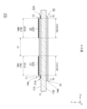
- Fig. 19 is a cross-sectional view of the quartz crystal vibrating element according to the second embodiment.
- the outer edge 71 of the first excitation electrode 14a overlaps the outer edge 81 of the second excitation electrode 14b, and the outer edge 72 of the first excitation electrode 14a overlaps the outer edge 82 of the second excitation electrode 14b.
- the outer edge 21A of the first part 21 and the outer edge 22A of the second part 22 of the mass addition film 20 are located between the outer edge 71 and the outer edge 72 of the first excitation electrode 14a.
- both the outer edge 71 of the first excitation electrode 14a and the outer edge 81 of the second excitation electrode 14b are farther from the center of the first excitation electrode 14a than the outer edge of the first low sound velocity region 18A.
- the outer edge 71 and the outer edge 81 are equally far from the center of the first excitation electrode 14a.
- Both the outer edge 71 of the first excitation electrode 14a and the outer edge 81 of the second excitation electrode 14b are farther from the center of the first excitation electrode 14a than the outer edge of the second low sound velocity region 18B.
- the outer edge 72 and the outer edge 82 are equally far from the center of the first excitation electrode 14a.
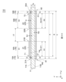
- Fig. 20 is a cross-sectional view of the quartz crystal vibrating element according to the third embodiment.
- the outer edge 81 of the second excitation electrode 14b is located between the outer edge 71 of the first excitation electrode 14a and the outer edge 21A of the first part 21 of the mass addition film 20.
- the outer edge 82 of the second excitation electrode 14b is located between the outer edge 72 of the first excitation electrode 14a and the outer edge 22A of the second part 22 of the mass addition film 20.
- the outer edge 21A of the first part 21 and the outer edge 22A of the second part 22 of the mass addition film 20 are located between the outer edge 81 and the outer edge 82 of the second excitation electrode 14b.
- the outer edge 81 and the outer edge 82 of the second excitation electrode 14b are located between the outer edge 71 and the outer edge 72 of the first excitation electrode 14a.
- Length B is greater than length C, and length C is greater than length A (A ⁇ C ⁇ B).
- both the outer edge 71 of the first excitation electrode 14a and the outer edge 81 of the second excitation electrode 14b are farther from the center of the first excitation electrode 14a than the outer edge of the first low sonic velocity region 18A.
- the outer edge 71 is farther from the center of the first excitation electrode 14a than the outer edge 81.
- Both the outer edge 71 of the first excitation electrode 14a and the outer edge 81 of the second excitation electrode 14b are farther from the center of the first excitation electrode 14a than the outer edge of the second low sonic velocity region 18B.
- the outer edge 72 is farther from the center of the first excitation electrode 14a than the outer edge 82.
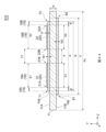
- Fig. 21 is a cross-sectional view of the quartz crystal vibrating element according to the fourth embodiment.
- the outer edge of the first low acoustic velocity region 18A overlaps not only the outer edge 21A of the first portion 21 of the mass-adding film 20, but also the outer edge 81 of the second excitation electrode 14b.
- the outer edge of the second low acoustic velocity region 18B overlaps not only the outer edge 22A of the second portion 22 of the mass-adding film 20, but also the outer edge 82 of the second excitation electrode 14b.
- one of the outer edge portions 71 of the first excitation electrode 14a and the outer edge portion 81 of the second excitation electrode 14b is farther from the center of the first excitation electrode 14a than the outer edge portion of the first low sonic velocity region 18A.
- One of the outer edge portions 72 of the first excitation electrode 14a and the outer edge portion 82 of the second excitation electrode 14b is farther from the center of the first excitation electrode 14a than the outer edge portion of the second low sonic velocity region 18B.
- Figs. 22 and 23 are diagrams for explaining the influence of misalignment in the fourth embodiment.
- Fig. 22 is a cross-sectional view of the quartz vibration element 410 when the mass addition film 20 is misaligned by dz in the positive direction of the Z' axis.
- Fig. 23 is a cross-sectional view of the quartz vibration element 410 when the second excitation electrode 14b is misaligned by dz in the negative direction of the Z' axis.
- the second portion 22 of the mass addition film 20 extends from the second excitation electrode 14b toward the positive side of the Z' axis by the amount of displacement dz. Therefore, the area where the first excitation electrode 14a, the second excitation electrode 14b, and the second portion 22 of the mass addition film 20 overlap is reduced by the amount of displacement dz.
- the length E1d1 and the length E2d2 do not change from the length E1.
- the second excitation electrode 14b when the second excitation electrode 14b is shifted in the Z'-axis positive direction by dz, the balance of the lengths of the first low sound velocity region 18A and the second low sound velocity region 18B along the Z'-axis direction changes, and the relationship E2d2 ⁇ E1d2 holds.
- the outer edge 22A of the second part 22 of the mass addition film 20 is located on the Z'-axis positive side of the second low sound velocity region 18B, and the outer edge 72 of the first excitation electrode 14a is located further on the Z'-axis positive side.
- the total thickness of the quartz vibration element 410 changes from Tp+Te1+Te2+Tf to Tp+Te1+Tf, then to Tp+Te1, and finally to Tp.
- the total thickness of the quartz vibration element 410 decreases stepwise, accelerating the phase change. This alleviates problems caused by a change in the balance of the lengths of the first low acoustic velocity region 18A and the second low acoustic velocity region 18B along the Z' axis direction.
- Fig. 24 is a cross-sectional view of the quartz crystal vibrating element according to the fifth embodiment.
- the outer edge 21A of the first portion 21 of the mass addition film 20 overlaps the outer edge 71 of the first excitation electrode 14a, and the outer edge 22A of the second portion 22 of the mass addition film 20 overlaps the outer edge 72 of the first excitation electrode 14a.
- the outer edge 21A of the first portion 21 and the outer edge 22A of the second portion 22 of the mass addition film 20 are located between the outer edge 81 and the outer edge 82 of the second excitation electrode 14b.
- the outer edge of the first low acoustic velocity region 18A overlaps not only the outer edge 21A of the first portion 21 of the mass-adding film 20, but also the outer edge 71 of the first excitation electrode 14a.
- the outer edge of the second low acoustic velocity region 18B overlaps not only the outer edge 22A of the second portion 22 of the mass-adding film 20, but also the outer edge 72 of the first excitation electrode 14a.
- one of the outer edge portions 71 of the first excitation electrode 14a and the outer edge portion 81 of the second excitation electrode 14b is farther from the center of the first excitation electrode 14a than the outer edge portion of the first low sonic velocity region 18A.
- One of the outer edge portions 72 of the first excitation electrode 14a and the outer edge portion 82 of the second excitation electrode 14b is farther from the center of the first excitation electrode 14a than the outer edge portion of the second low sonic velocity region 18B.
- Figs. 25 and 26 are diagrams for explaining the influence of misalignment in the fifth embodiment.
- Fig. 25 is a cross-sectional view of the quartz vibration element 510 when the mass addition film 20 is misaligned by dz in the positive direction of the Z' axis.
- Fig. 26 is a cross-sectional view of the quartz vibration element 510 when the second excitation electrode 14b is misaligned by dz in the negative direction of the Z' axis.
- the outer edge 22A of the second part 22 of the mass addition film 20 is located between the outer edge 72 of the first excitation electrode 14a and the outer edge 82 of the second excitation electrode 14b in a plan view.
- the outer edge 71 of the first excitation electrode 14a is located between the outer edge 21A of the first part 21 of the mass addition film 20 and the outer edge 81 of the second excitation electrode 14b.
- the second part 22 of the mass addition film 20 extends from the first excitation electrode 14a in the positive direction of the Z' axis by the shift amount dz.
- the difference in length along the Z'-axis direction between the first low sound velocity region and the second low sound velocity region when the mass addition film is shifted by dz in the positive direction of the Z'-axis in the comparative example is dz. Therefore, in this embodiment, the deterioration of the electromechanical coupling coefficient k when the mass addition film 20 is shifted is equivalent to the deterioration of the electromechanical coupling coefficient k when the mass addition film is shifted in the comparative example.
- the second excitation electrode when the second excitation electrode is shifted by dz in the negative direction of the Z' axis in the comparative example, the difference in the lengths of the first low sound velocity region and the second low sound velocity region along the Z' axis direction is dz. Therefore, in this embodiment, the deterioration of the electromechanical coupling coefficient k when the second excitation electrode is shifted in the negative direction of the Z' axis is suppressed more than the deterioration of the electromechanical coupling coefficient k when the second excitation electrode is shifted in the comparative example. In other words, even if the second excitation electrode 14b is shifted by dz in the negative direction of the Z' axis, the increase in k_A0 is suppressed and the decrease in k_S0 is suppressed.
- Fig. 27 is a cross-sectional view of the quartz crystal vibrating element according to the sixth embodiment.
- the mass-adding film 20 is made of an insulating material, such as silicon oxide or silicon nitride.
- the outer edge 21A of the first portion 21 of the mass-adding film 20 overlaps the outer edge 81 of the second excitation electrode 14b
- the outer edge 22A of the second portion 22 of the mass-adding film 20 overlaps the outer edge 82 of the second excitation electrode 14b.
- the outer edges 71 and 72 of the first excitation electrode 14a are located between the outer edges 21A and 22A of the first portion 21 of the mass-adding film 20.
- the length E1 is smaller than the length D1 (D1 ⁇ E1)
- the length E2 is smaller than the length D2 (D2 ⁇ E2)
- the outer edge of the first low sound velocity region 18A overlaps with the outer edge 71 of the first excitation electrode 14a.
- the outer edge of the second low sound velocity region 18B overlaps with the outer edge 72 of the first excitation electrode 14a.
- Figs. 28 and 29 are diagrams for explaining the influence of misalignment in the sixth embodiment.
- Fig. 28 is a cross-sectional view of the quartz vibration element 610 when the mass addition film 20 is misaligned by dz in the positive direction of the Z' axis.
- Fig. 29 is a cross-sectional view of the quartz vibration element 610 when the second excitation electrode 14b is misaligned by dz in the negative direction of the Z' axis.
- Fig. 30 is a cross-sectional view of the quartz crystal vibrating element according to the seventh embodiment.
- the material of the mass-adding film 20 is an electrical conductor, for example, the same material as the first excitation electrode 14a.
- the outer edge 21A of the first part 21 of the mass-adding film 20 overlaps the outer edge 81 of the second excitation electrode 14b
- the outer edge 22A of the second part 22 of the mass-adding film 20 overlaps the outer edge 82 of the second excitation electrode 14b.
- the outer edges 71, 72 of the first excitation electrode 14a are located between the outer edges 21A and 22A of the first part 21 of the mass-adding film 20.
- the outer edge of the first low sound velocity region 18A overlaps with the outer edge 71 of the first excitation electrode 14a.
- the outer edge of the second low sound velocity region 18B overlaps with the outer edge 72 of the first excitation electrode 14a.
- the outer edge 21A of the first portion 21 of the mass-adding film 20 and the outer edge 81 of the second excitation electrode 14b are both farther away from the center of the first excitation electrode 14a than the outer edge of the first low sound velocity region 18A.
- the outer edge 21A and the outer edge 81 are equally far from the center of the first excitation electrode 14a.
- the outer edge 22A of the second portion 22 of the mass-adding film 20 and the outer edge 82 of the second excitation electrode 14b are both farther away from the center of the first excitation electrode 14a than the outer edge of the second low sound velocity region 18B.
- the outer edge 22A and the outer edge 82 are equally far from the center of the first excitation electrode 14a.
- the first portion 21 of the mass addition film 2 extends from the first excitation electrode 14a in the negative Z' direction.
- the second portion 22 of the mass addition film 2 extends from the first excitation electrode 14a in the positive Z' direction. Since the mass addition film 20 has the same potential as the first excitation electrode 14a, the portion of the mass addition film 20 extending from the first excitation electrode 14a functions as an excitation electrode. Therefore, in a planar view, the area outside the first excitation electrode 14a where the first portion 21 of the mass addition film 20 and the second excitation electrode 14b overlap becomes the first outer high sound velocity area 191A, and the area outside the first excitation electrode 14a where the second portion 22 of the mass addition film 20 and the second excitation electrode 14b overlap becomes the second outer high sound velocity area 191B.
- the sum of the thicknesses in the high acoustic velocity region 17 is Tp+Te1+Te2, and the sum of the thicknesses in the first outer high acoustic velocity region 191A and the second outer high acoustic velocity region 191B is Tp+Tf+Te2. Therefore, when the material of the mass addition film 20 is the same as the material of the first excitation electrode 14a and the relationship Tf ⁇ Te1 is established, the sound velocity in the first outer high acoustic velocity region 191A and the second outer high acoustic velocity region 191B is greater than the sound velocity in the high acoustic velocity region 17.
- the sound velocity in the high acoustic velocity region 17 is smaller than the sound velocity in the outer high acoustic velocity region 191, and the sound velocity in the low acoustic velocity region 18 is smaller than the sound velocity in the high acoustic velocity region 17.
- the sound velocity in the first outer high sound velocity region 191A and the second outer high sound velocity region 191B is approximately equal to the sound velocity in the high sound velocity region 17.
- the sound velocity in the outer high sound velocity region 191 and the sound velocity in the high sound velocity region 17 are approximately equal and are greater than the sound velocity in the low sound velocity region 18.
- the sound velocity in the first outer high sound velocity region 191A and the second outer high sound velocity region 191B is smaller than the sound velocity in the high sound velocity region 17.
- the sound velocity in the outer high sound velocity region 191 is smaller than the sound velocity in the high sound velocity region 17
- the sound velocity in the low sound velocity region 18 is smaller than the sound velocity in the outer high sound velocity region 191.
- the sound velocity of the outer high sound velocity region 191 may be smaller than that of the high sound velocity region 17 even when the relationship Tf ⁇ Te1 is established.
- the sound velocity of the outer high sound velocity region 191 is smaller than that of the high sound velocity region 17.
- the mass per unit area of the mass-adding film 20 is equivalent to that of the first excitation electrode 14a
- the sound velocity of the outer high sound velocity region 191 is equivalent to that of the high sound velocity region 17.
- the mass per unit area of the mass-adding film 20 is smaller than that of the first excitation electrode 14a, the sound velocity of the outer high sound velocity region 191 is larger than that of the high sound velocity region 17.
- Fig. 31 is a cross-sectional view of the quartz crystal vibrating element according to the eighth embodiment.
- the outer edge 21A of the first part 21 and the outer edge 22A of the second part 22 of the mass addition film 20 are located between the outer edge 81 and the outer edge 82 of the second excitation electrode 14b.
- the outer edge 71 of the first excitation electrode 14a is located between the outer edge 21A of the first part 21 of the mass addition film 20 and the outer edge 81 of the second excitation electrode 14b.
- the outer edge 72 of the first excitation electrode 14a is located between the outer edge 22A of the second part 22 of the mass addition film 20 and the outer edge 82 of the second excitation electrode 14b.
- the length A is greater than the length B and less than the length C (B ⁇ A ⁇ C).
- the outer edge of the first low sound velocity region 18A overlaps with the outer edge 71 of the first excitation electrode 14a.
- the outer edge of the second low sound velocity region 18B overlaps with the outer edge 72 of the first excitation electrode 14a.
- the outer edge 21A of the first portion 21 of the mass-adding film 20 and the outer edge 81 of the second excitation electrode 14b are both farther from the center of the first excitation electrode 14a than the outer edge of the first low acoustic velocity region 18A.
- the outer edge 81 is farther from the center of the first excitation electrode 14a than the outer edge 21A.
- the outer edge 22A of the second portion 22 of the mass-adding film 20 and the outer edge 82 of the second excitation electrode 14b are both farther from the center of the first excitation electrode 14a than the outer edge of the second low acoustic velocity region 18B.
- the outer edge 82 is about the same distance from the center of the first excitation electrode 14a as the outer edge 22A.
- Fig. 32 is a table showing the simulation results of the comparative example and examples based on the first to eighth embodiments.
- Fig. 33 is a table showing the simulation conditions of the comparative example and examples based on the first to eighth embodiments.
- “Frame misalignment” means that the position of the mass adding film 20 is misaligned with respect to the positions of the first excitation electrode 14a and the second excitation electrode 14b.
- “Back surface misalignment” means that the position of the second excitation electrode 14b is misaligned with respect to the positions of the mass adding film 20 and the first excitation electrode 14a.
- “Both misalignments” means that the position of the mass adding film 20 is misaligned with respect to the position of the first excitation electrode 14a, and the position of the second excitation electrode 14b is misaligned with respect to the position of the first excitation electrode 14a in the opposite direction to the misalignment of the mass adding film 20.
- the change in k ⁇ k due to frame shift in S0 mode is -0.15%
- the change in k ⁇ k due to backside shift in S0 mode is -0.04%
- the change in k ⁇ k due to both shifts in S0 mode is -0.28%.
- the change in k ⁇ k due to frame shift in A0Z mode is 1.07%
- the change in k ⁇ k due to backside shift in A0Z mode is 0.69%
- the change in k ⁇ k due to both shifts in A0Z mode is 1.43%.
- the change in k ⁇ k due to frame misalignment in S0 mode is 0.00%
- the change in k ⁇ k due to back surface misalignment in S0 mode is 0.00%
- the change in k ⁇ k due to both misalignments in S0 mode is 0.00%.
- the ⁇ k in S0 mode in the example based on the first embodiment is smaller than the ⁇ k in S0 mode in the comparative example. That is, in the example based on the first embodiment, the decrease in k in S0 mode due to position misalignment is suppressed.
- the change in k ⁇ k due to frame misalignment in the A0Z mode is 0.02%
- the change in k ⁇ k due to backside misalignment in the A0Z mode is 0.05%
- the change in k ⁇ k due to both sides misalignment in the A0Z mode is 0.02%.
- the ⁇ k of the A0Z mode in the example based on the first embodiment is smaller than the ⁇ k of the A0Z mode in the comparative example. That is, in the example based on the first embodiment, the increase in k in the A0Z mode due to position misalignment is suppressed.
- the change in k ⁇ k due to frame shift in S0 mode is 0.00%
- the change in k ⁇ k due to backside shift in S0 mode is 0.01%
- the change in k ⁇ k due to both shifts in S0 mode is 0.01%.
- the change in k ⁇ k due to frame shift in A0Z mode is 0.03%
- the change in k ⁇ k due to backside shift in A0Z mode is 0.06%
- the change in k ⁇ k due to both shifts in A0Z mode is 0.05%.
- the change in k ⁇ k due to frame shift in S0 mode is -0.01%
- the change in k ⁇ k due to backside shift in S0 mode is -0.02%
- the change in k ⁇ k due to both shifts in S0 mode is -0.06%.
- the change in k ⁇ k due to frame shift in A0Z mode is 0.17%
- the change in k ⁇ k due to backside shift in A0Z mode is 0.19%
- the change in k ⁇ k due to both shifts in A0Z mode is 0.35%.
- the change in k ⁇ k due to frame shift in S0 mode is -0.01%
- the change in k ⁇ k due to backside shift in S0 mode is -0.02%
- the change in k ⁇ k due to both shifts in S0 mode is -0.06%.
- the change in k ⁇ k due to frame shift in A0Z mode is 0.34%
- the change in k ⁇ k due to backside shift in A0Z mode is 0.36%
- the change in k ⁇ k due to both shifts in A0Z mode is 0.51%.
- the decrease in k in the S0 mode caused by misalignment is suppressed.
- the increase in k in the A0Z mode caused by misalignment is suppressed.
- the change in k ⁇ k due to frame shift in S0 mode is -0.13%
- the change in k ⁇ k due to backside shift in S0 mode is 0.00%
- the change in k ⁇ k due to both shifts in S0 mode is -0.14%.
- the change in k ⁇ k due to frame shift in A0Z mode is 0.89%
- the change in k ⁇ k due to backside shift in A0Z mode is 0.02%
- the change in k ⁇ k due to both shifts in A0Z mode is 0.96%.
- the change in k ⁇ k due to frame shift in S0 mode is -0.13%
- the change in k ⁇ k due to backside shift in S0 mode is 0.00%
- the change in k ⁇ k due to both shifts in S0 mode is -0.15%.
- the change in k ⁇ k due to frame shift in A0Z mode is 1.01%
- the change in k ⁇ k due to backside shift in A0Z mode is 0.03%
- the change in k ⁇ k due to both shifts in A0Z mode is 1.06%.
- the ⁇ k of the S0 mode and the ⁇ k of the A0Z mode in frame shear are approximately equivalent to the ⁇ k of the S0 mode and the ⁇ k of the A0Z mode in the comparative example.
- the decrease in ⁇ k of the S0 mode in backside shear and both shear is suppressed, and the increase in ⁇ k of the A0Z mode in backside shear and both shear is suppressed.
- the change in k ⁇ k due to frame shift in S0 mode is -0.20%
- the change in k ⁇ k due to backside shift in S0 mode is 0.00%
- the change in k ⁇ k due to both shifts in S0 mode is -0.22%.
- the change in k ⁇ k due to frame shift in A0Z mode is 1.27%
- the change in k ⁇ k due to backside shift in A0Z mode is 0.11%
- the change in k ⁇ k due to both shifts in A0Z mode is 1.31%.
- the change in k ⁇ k due to frame shift in S0 mode is -0.18%
- the change in k ⁇ k due to backside shift in S0 mode is 0.00%
- the change in k ⁇ k due to both shifts in S0 mode is -0.19%.
- the change in k ⁇ k due to frame shift in A0Z mode is 1.29%
- the change in k ⁇ k due to backside shift in A0Z mode is 0.07%
- the change in k ⁇ k due to both shifts in A0Z mode is 1.31%.
- the ⁇ k of the S0 mode and the ⁇ k of the A0Z mode in frame misalignment are slightly worse than the ⁇ k of the S0 mode and the ⁇ k of the A0Z mode in the comparative example.
- the decrease in ⁇ k of the S0 mode in backside misalignment and both misalignments is suppressed, and the increase in ⁇ k of the A0Z mode in backside misalignment and both misalignments is suppressed.
- FIG. 34 is a cross-sectional view of the quartz crystal vibration element according to the ninth embodiment.
- the mass-adding film 20 is made of a metal different from that of the first excitation electrode 14a. From the viewpoint of efficiently adding mass and reducing the sound velocity in the low sound velocity region 18, it is desirable that the specific gravity of the mass-adding film 20 is greater than the specific gravity of the first excitation electrode 14a. This makes it possible to shorten the film formation process of the mass-adding film 20 and improve manufacturing efficiency.
- FIG. 35 is a plan view of the quartz crystal vibration element according to the tenth embodiment.
- the third portion 23 and the fourth portion 24 of the mass-adding film 20 are omitted.
- the first portion 21 and the second portion 22 of the mass-adding film 20 are spaced apart from each other and are arranged in a band shape extending along the X-axis direction.
- FIG. 36 is a plan view of the quartz crystal vibration element according to the 11th embodiment.
- the first portion 21 and the second portion 22 of the mass-adding film 20 are omitted.
- the third portion 23 and the fourth portion 24 of the mass-adding film 20 are spaced apart from each other and are arranged in a band shape extending along the Z'-axis direction.
- a piezoelectric piece having a first main surface extending in a first direction and a second direction intersecting the first direction, and a second main surface facing the first main surface; a first excitation electrode provided on a first main surface of the piezoelectric piece; a second excitation electrode provided on a second main surface of the piezoelectric piece; a mass-adding film at least partially overlapping the first excitation electrode; the mass addition film includes a first portion and a second portion provided to avoid a central portion of the first excitation electrode, the first excitation electrode has, in a plan view, a first outer edge portion located on one side in the first direction with respect to a central portion, and a second outer edge portion located on the other side in the first direction with respect to the central portion; the second excitation electrode has, in a plan view, a third outer edge portion located on one side in the first direction with respect to a central portion, and a fourth outer edge portion located on the other side in the first direction with respect to the central portion;
- the first portion is
- the material of the mass-added membrane is an electrical conductor.
- the material of the mass-added membrane is an insulator.
- ⁇ 15> In the mass addition film, a distance in a first direction between an end of the first portion opposite to the second portion side and an end of the second portion opposite to the first portion side is defined as A', and a dimension of the first excitation electrode in the first direction is defined as B. A'/B ⁇ 0.5
- the relationship is established as follows: ⁇ 1> The piezoelectric vibration element according to any one of ⁇ 1> to ⁇ 14>.
- a distance along a first direction between an outer edge portion located on one side of the first portion of the mass addition film and a first outer edge portion of the first excitation electrode, and a distance along the first direction between an outer edge portion located on the other side of the second portion of the mass addition film and a second outer edge portion of the first excitation electrode are 0.5 ⁇ m or more;
- a distance along a first direction between an outer edge portion located on one side of the first portion of the mass addition film and a first outer edge portion of the first excitation electrode, and a distance along the first direction between an outer edge portion located on the other side of the second portion of the mass addition film and a second outer edge portion of the first excitation electrode are 8 ⁇ m or less;
- the mass addition film includes a third portion and a fourth portion provided to avoid a central portion of the first excitation electrode
- the first excitation electrode has, in a plan view, a fifth outer edge portion located on one side in the second direction with respect to a central portion, and a sixth outer edge portion located on the other side in the second direction with respect to the central portion
- the second excitation electrode has, in a plan view, a seventh outer edge portion located on one side in the second direction with respect to the central portion, and an eighth outer edge portion located on the other side in the second direction with respect to the central portion
- the third portion is disposed along the fifth outer edge
- the fourth portion is disposed along the sixth outer edge
- the mass addition film includes a third portion and a fourth portion provided to avoid a central portion of the first excitation electrode
- the first excitation electrode has, in a plan view, a fifth outer edge portion located on one side in the second direction with respect to a central portion, and a sixth outer edge portion located on the other side in the second direction with respect to the central portion
- the second excitation electrode has, in a plan view, a seventh outer edge portion located on one side in the second direction with respect to the central portion, and an eighth outer edge portion located on the other side in the second direction with respect to the central portion
- the third portion is disposed along the fifth outer edge
- the fourth portion is disposed along the sixth outer edge, a region where the piezoelectric piece, the first excitation electrode, and the second excitation electrode are further overlapped by a third portion of the mass addition film is defined as a third low sound velocity region, and a region where the piezoelectric piece, the first excitation electrode, and the second excitation electrode are further overlapped by a fourth portion of the mass
- the first excitation electrode has, in a plan view, a fifth outer edge portion located on one side in the second direction with respect to a central portion, and a sixth outer edge portion located on the other side in the second direction with respect to the central portion; When viewed in a plan view, the fifth outer edge portion and the sixth outer edge portion overlap the second excitation electrode.
- the piezoelectric vibration element according to any one of ⁇ 1> to ⁇ 22>.
- the piezoelectric strip is a quartz crystal strip.
- the piezoelectric vibration element according to any one of ⁇ 1> to ⁇ 23>.
- the cut angle of the quartz crystal piece is AT cut, BT cut or ST cut.
- the main vibration mode is thickness-shear vibration.
- the piezoelectric vibration element according to any one of ⁇ 1> to ⁇ 25>.
- the embodiment of the present invention is not limited to quartz crystal resonators, but can also be applied to other piezoelectric resonators (Piezoelectric Resonator Units).
- piezoelectric pieces suitable for use in the piezoelectric resonator of this embodiment include piezoelectric ceramics such as lead zirconate titanate (PZT) and aluminum nitride, and piezoelectric single crystals such as lithium niobate and lithium tantalate, but the present invention is not limited to these and can be selected as appropriate.
- Embodiments of the present invention can be applied as appropriate to any device that performs electromechanical energy conversion using the piezoelectric effect, such as a timing device, sound generator, oscillator, or load sensor, without any particular limitations.
- one aspect of the present invention provides a piezoelectric vibration element that can suppress deterioration of the electromechanical coupling coefficient.
Landscapes
- Physics & Mathematics (AREA)
- Acoustics & Sound (AREA)
- Piezo-Electric Or Mechanical Vibrators, Or Delay Or Filter Circuits (AREA)
Priority Applications (3)
| Application Number | Priority Date | Filing Date | Title |
|---|---|---|---|
| JP2024555027A JP7718606B2 (ja) | 2023-07-19 | 2024-04-01 | 圧電振動素子 |
| CN202480003841.XA CN119836747A (zh) | 2023-07-19 | 2024-04-01 | 压电振动元件 |
| US19/044,813 US20250183873A1 (en) | 2023-07-19 | 2025-02-04 | Piezoelectric vibration element |
Applications Claiming Priority (2)
| Application Number | Priority Date | Filing Date | Title |
|---|---|---|---|
| JP2023117392 | 2023-07-19 | ||
| JP2023-117392 | 2023-07-19 |
Related Child Applications (1)
| Application Number | Title | Priority Date | Filing Date |
|---|---|---|---|
| US19/044,813 Continuation US20250183873A1 (en) | 2023-07-19 | 2025-02-04 | Piezoelectric vibration element |
Publications (1)
| Publication Number | Publication Date |
|---|---|
| WO2025017976A1 true WO2025017976A1 (ja) | 2025-01-23 |
Family
ID=94282028
Family Applications (1)
| Application Number | Title | Priority Date | Filing Date |
|---|---|---|---|
| PCT/JP2024/013407 Pending WO2025017976A1 (ja) | 2023-07-19 | 2024-04-01 | 圧電振動素子 |
Country Status (4)
| Country | Link |
|---|---|
| US (1) | US20250183873A1 (https=) |
| JP (1) | JP7718606B2 (https=) |
| CN (1) | CN119836747A (https=) |
| WO (1) | WO2025017976A1 (https=) |
Citations (5)
| Publication number | Priority date | Publication date | Assignee | Title |
|---|---|---|---|---|
| JPH031710A (ja) * | 1989-05-30 | 1991-01-08 | Kinseki Ltd | 圧電振動子 |
| US6111341A (en) * | 1997-02-26 | 2000-08-29 | Toyo Communication Equipment Co., Ltd. | Piezoelectric vibrator and method for manufacturing the same |
| WO2021112214A1 (ja) * | 2019-12-06 | 2021-06-10 | 株式会社村田製作所 | 弾性波装置 |
| WO2022080426A1 (ja) * | 2020-10-13 | 2022-04-21 | 株式会社村田製作所 | 水晶振動素子および水晶振動子 |
| JP2022153702A (ja) * | 2021-03-30 | 2022-10-13 | 株式会社大真空 | 圧電フィルタ |
-
2024
- 2024-04-01 JP JP2024555027A patent/JP7718606B2/ja active Active
- 2024-04-01 WO PCT/JP2024/013407 patent/WO2025017976A1/ja active Pending
- 2024-04-01 CN CN202480003841.XA patent/CN119836747A/zh active Pending
-
2025
- 2025-02-04 US US19/044,813 patent/US20250183873A1/en active Pending
Patent Citations (5)
| Publication number | Priority date | Publication date | Assignee | Title |
|---|---|---|---|---|
| JPH031710A (ja) * | 1989-05-30 | 1991-01-08 | Kinseki Ltd | 圧電振動子 |
| US6111341A (en) * | 1997-02-26 | 2000-08-29 | Toyo Communication Equipment Co., Ltd. | Piezoelectric vibrator and method for manufacturing the same |
| WO2021112214A1 (ja) * | 2019-12-06 | 2021-06-10 | 株式会社村田製作所 | 弾性波装置 |
| WO2022080426A1 (ja) * | 2020-10-13 | 2022-04-21 | 株式会社村田製作所 | 水晶振動素子および水晶振動子 |
| JP2022153702A (ja) * | 2021-03-30 | 2022-10-13 | 株式会社大真空 | 圧電フィルタ |
Also Published As
| Publication number | Publication date |
|---|---|
| JP7718606B2 (ja) | 2025-08-05 |
| CN119836747A (zh) | 2025-04-15 |
| JPWO2025017976A1 (https=) | 2025-01-23 |
| US20250183873A1 (en) | 2025-06-05 |
Similar Documents
| Publication | Publication Date | Title |
|---|---|---|
| JP5957997B2 (ja) | 振動素子、振動子、電子デバイス、発振器、及び電子機器 | |
| US12438517B2 (en) | Quartz vibration element and manufacturing method of quartz vibration element | |
| CN113765494A (zh) | 振子以及振荡器 | |
| JP2000278079A (ja) | 圧電デバイス | |
| JP7465454B2 (ja) | 圧電振動素子、圧電振動子及び電子装置 | |
| JP7517135B2 (ja) | 圧電振動デバイス | |
| JP7718606B2 (ja) | 圧電振動素子 | |
| JP7665133B2 (ja) | 圧電振動素子 | |
| JP7605025B2 (ja) | 圧電振動デバイス | |
| JP6278061B2 (ja) | 振動素子、振動子、電子デバイス、発振器、及び電子機器 | |
| JP7606679B2 (ja) | 圧電振動素子、圧電振動子及び圧電発振器 | |
| JP7773705B1 (ja) | 圧電振動素子 | |
| JP7691035B1 (ja) | 圧電振動素子 | |
| US20250141426A1 (en) | Piezoelectric resonator | |
| WO2025258357A1 (ja) | 基板及び圧電振動子 | |
| JP7626216B2 (ja) | 圧電振動板および圧電振動デバイス | |
| WO2025182135A1 (ja) | 圧電振動子 | |
| WO2026078949A1 (ja) | 圧電振動素子 | |
| WO2025150245A1 (ja) | 圧電振動子 | |
| WO2024176856A1 (ja) | 2回回転水晶振動板 | |
| WO2021220544A1 (ja) | 圧電振動子及びそれを備える圧電発振器 | |
| JP2025144332A (ja) | 発振器 | |
| WO2022158028A1 (ja) | 圧電振動子 | |
| WO2021215040A1 (ja) | 圧電振動子 | |
| JP2012160995A (ja) | 振動片、振動子、発振器及び電子機器 |
Legal Events
| Date | Code | Title | Description |
|---|---|---|---|
| WWE | Wipo information: entry into national phase |
Ref document number: 2024555027 Country of ref document: JP |
|
| WWE | Wipo information: entry into national phase |
Ref document number: 202480003841.X Country of ref document: CN |
|
| 121 | Ep: the epo has been informed by wipo that ep was designated in this application |
Ref document number: 24842777 Country of ref document: EP Kind code of ref document: A1 |
|
| WWP | Wipo information: published in national office |
Ref document number: 202480003841.X Country of ref document: CN |
|
| NENP | Non-entry into the national phase |
Ref country code: DE |