WO2025013681A1 - 半導体装置 - Google Patents
半導体装置 Download PDFInfo
- Publication number
- WO2025013681A1 WO2025013681A1 PCT/JP2024/023782 JP2024023782W WO2025013681A1 WO 2025013681 A1 WO2025013681 A1 WO 2025013681A1 JP 2024023782 W JP2024023782 W JP 2024023782W WO 2025013681 A1 WO2025013681 A1 WO 2025013681A1
- Authority
- WO
- WIPO (PCT)
- Prior art keywords
- gate
- shield
- wiring
- electrode
- pad portion
- Prior art date
- Legal status (The legal status is an assumption and is not a legal conclusion. Google has not performed a legal analysis and makes no representation as to the accuracy of the status listed.)
- Pending
Links
Images





Classifications
-
- H—ELECTRICITY
- H10—SEMICONDUCTOR DEVICES; ELECTRIC SOLID-STATE DEVICES NOT OTHERWISE PROVIDED FOR
- H10D—INORGANIC ELECTRIC SEMICONDUCTOR DEVICES
- H10D12/00—Bipolar devices controlled by the field effect, e.g. insulated-gate bipolar transistors [IGBT]
-
- H—ELECTRICITY
- H10—SEMICONDUCTOR DEVICES; ELECTRIC SOLID-STATE DEVICES NOT OTHERWISE PROVIDED FOR
- H10D—INORGANIC ELECTRIC SEMICONDUCTOR DEVICES
- H10D30/00—Field-effect transistors [FET]
- H10D30/01—Manufacture or treatment
-
- H—ELECTRICITY
- H10—SEMICONDUCTOR DEVICES; ELECTRIC SOLID-STATE DEVICES NOT OTHERWISE PROVIDED FOR
- H10D—INORGANIC ELECTRIC SEMICONDUCTOR DEVICES
- H10D30/00—Field-effect transistors [FET]
- H10D30/60—Insulated-gate field-effect transistors [IGFET]
- H10D30/64—Double-diffused metal-oxide semiconductor [DMOS] FETs
- H10D30/66—Vertical DMOS [VDMOS] FETs
-
- H—ELECTRICITY
- H10—SEMICONDUCTOR DEVICES; ELECTRIC SOLID-STATE DEVICES NOT OTHERWISE PROVIDED FOR
- H10D—INORGANIC ELECTRIC SEMICONDUCTOR DEVICES
- H10D62/00—Semiconductor bodies, or regions thereof, of devices having potential barriers
- H10D62/10—Shapes, relative sizes or dispositions of the regions of the semiconductor bodies; Shapes of the semiconductor bodies
Definitions
- This disclosure relates to a semiconductor device equipped with a semiconductor switching element having a double-gate trench gate structure.
- a semiconductor device including a power MOSFET having a double-gate trench gate structure as shown in, for example, Patent Document 1 is known.
- a double-gate trench gate structure is formed in a surface layer of a semiconductor substrate having an n- type drift layer formed on an n + type substrate.
- a shield electrode that is set to a source potential is disposed on the bottom side of the gate trench via a shield insulating film.
- a gate electrode layer is disposed on the upper side of the shield electrode in the trench via a gate insulating film to form a double gate.
- An interlayer insulating film (hereinafter referred to as an intermediate insulating film) is formed between the shield electrode and the gate electrode layer, and the intermediate insulating film insulates the shield electrode from the gate electrode layer.
- the shield electrode is designed to have the same potential as the source potential, that is, the upper electrode equivalent to the source electrode and the source region, and the shield wiring connected to the shield electrode is directly connected to the upper electrode.
- the purpose of this disclosure is to provide a structure that allows accurate screening of the insulating films of each part included in a trench gate structure in a semiconductor device equipped with a semiconductor switching element having a double-gate trench gate structure.
- One aspect of the present disclosure is a method for producing a cellular membrane comprising: A semiconductor device including a semiconductor switching element having a double-gate trench gate structure,
- the semiconductor switching element is A drift layer of a first conductivity type; a body region of a second conductivity type formed on the drift layer; an impurity region of a first conductivity type formed in a surface layer portion of the body region and having a higher impurity concentration than the drift layer; a plurality of trench gate structures each having a double gate formed by sequentially stacking a shield electrode, an intermediate insulating film, and a gate electrode layer in a plurality of gate trenches each having a longitudinal direction in one direction and arranged in a stripe shape extending from the impurity region through the body region to the drift layer, with an insulating film interposed therebetween; a first or second conductivity type high concentration layer formed on the opposite side of the drift layer from the body region and having a higher impurity concentration than the drift layer; an interlayer insulating film disposed on the
- the upper electrode is electrically isolated from the gate wiring and shield wiring.
- the upper electrode is electrically isolated from the gate electrode layer and shield electrode. This allows the potentials of the upper electrode, shield electrode and gate electrode layer to be individually controlled. Therefore, when screening the insulating film and intermediate insulating film disposed in the gate trench, it becomes possible to apply the desired voltage to the location to be inspected.
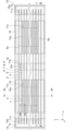
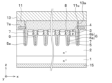
- FIG. 1 is a top view layout diagram of a semiconductor device according to a first embodiment of the present disclosure. This is a cross-sectional view taken along line IIA-IIA in FIG. This is a cross-sectional view taken along the line IIB-IIB in FIG.
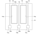
- FIG. 2 is a cross-sectional view taken along line III-III in FIG. 2 is a simplified top surface layout of the semiconductor device shown in FIG. 1 , showing a conductor portion on the top surface side in a see-through manner;
- FIG. 11 is a cross-sectional view of a semiconductor device according to a second embodiment of the present disclosure taken along the longitudinal direction of a trench gate structure. 6 is a top surface layout of the semiconductor device shown in FIG.
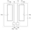
- FIG. 13 is a simplified top surface layout of a semiconductor device described in a modified example of the second embodiment, showing a conductor portion on the top surface side in a see-through manner.
- FIG. 11 is a top view layout diagram of a semiconductor device according to a third embodiment of the present disclosure.
- 9 is a simplified top surface layout of the semiconductor device shown in FIG. 8, showing a conductor portion on the top surface side in a see-through manner. This is a cross-sectional view taken along the line XX in Figure 8.
- FIG. 13 is a simplified top surface layout of a semiconductor device described in a modified example of the third embodiment, showing a conductor portion on the top surface side in a see-through manner.
- FIG. 13 is a simplified top surface layout of a semiconductor device described in a modified example of the third embodiment, showing a conductor portion on the top surface side in a see-through manner.
- FIG. 13 is a simplified top surface layout of a semiconductor device described in a modified example of the third embodiment, showing
- MOSFET n-channel vertical power MOSFET
- the width direction of the MOSFET is defined as the x direction
- the depth direction of the MOSFET that intersects with the x direction is defined as the y direction
- the thickness direction or depth direction of the MOSFET i.e., the normal direction to the xy plane, is defined as the z direction.
- the first pad portion 10b which will be described later, has been omitted in order to make the figure easier to understand.
- the semiconductor device according to this embodiment is formed using an n + type semiconductor substrate 1 made of a semiconductor material such as silicon having a high impurity concentration.
- An n- type drift layer 2 having a lower impurity concentration than the n + type semiconductor substrate 1 is formed on the surface of the n + type semiconductor substrate 1.
- a p-type body region 3 having a relatively low impurity concentration is formed at a desired position in the surface layer portion of the n - type drift layer 2.
- the p-type body region 3 is formed, for example, by ion implantation of p-type impurities into the n - type drift layer 2, and also functions as a channel layer that forms a channel region. As shown in FIG. 1, the p-type body region 3 is formed between a plurality of trench gate structures described later, with the y direction as the longitudinal direction.
- An n-type impurity region 4 corresponding to a source region having a higher impurity concentration than the n - type drift layer 2 is provided in a surface layer portion of the p-type body region 3.
- a contact trench 4a is formed in the n-type impurity region 4, and the p-type body region 3 is exposed at the bottom surface of the contact trench 4a.
- a p + type contact region 3a serving as a body contact is formed in the exposed portion of the p-type body region 3.
- an n + type contact region 4b serving as a source contact is formed on the side surface of the contact trench 4a in the n-type impurity region 4.
- a plurality of gate trenches 5 extending in one direction, the y direction here, are formed between the p-type body regions 3 and the n-type impurity regions 4 in the surface layer portion of the n ⁇ -type drift layer 2.
- These gate trenches 5 are trenches for forming a trench gate structure, and in this embodiment, the gate trenches 5 are arranged in parallel at equal intervals to form a striped layout.
- the gate trench 5 has a depth deeper than the p-type body region 3, that is, the depth of the gate trench 5 penetrates from the substrate surface side through the n-type impurity region 4 and the p-type body region 3 to the n ⁇ -type drift layer 2.
- the gate trench 5 is gradually narrowed toward the bottom, and the bottom is rounded.
- the inner wall surface of the gate trench 5 is covered with an insulating film 6.
- the insulating film 6 may be composed of a single film, but in this embodiment, it is composed of a shield insulating film 6a that covers the lower part of the gate trench 5 and a gate insulating film 6b that covers the upper part.
- the shield insulating film 6a covers the side surface of the gate trench 5 from the bottom to the lower part, and the gate insulating film 6b covers the side surface of the upper part of the gate trench 5.
- the shield insulating film 6a is formed thicker than the gate insulating film 6b.
- a shield electrode 7 and a gate electrode layer 8 made of doped poly-Si are stacked with an insulating film 6 interposed between them to form a double gate.
- the shield electrode 7 is fixed to the source potential, thereby reducing the capacitance between the gate and drain, and is formed to improve the electrical characteristics of the MOSFET. Furthermore, since the shield electrode 7 is provided, it is possible to two-dimensionally deplete the gap between a plurality of trench gate structures, and therefore, compared to a MOSFET having a single gate structure, a desired breakdown voltage can be obtained even if the thickness of the n - type drift layer 2 is thin. Furthermore, since the n - type drift layer 2 can be made thin, it is possible to realize a low on-resistance. However, in the semiconductor device described in this embodiment, the shield electrode 7 is separated from the source, and a voltage different from that of the source can be applied. Details of this structure will be described later.
- the gate electrode layer 8 performs the switching operation of the MOSFET, and forms a channel region in the p-type body region 3 on the side of the gate trench 5 when a gate voltage is applied.
- An intermediate insulating film 9 is formed between the shield electrode 7 and the gate electrode layer 8, and the shield electrode 7 and the gate electrode layer 8 are insulated by the intermediate insulating film 9.
- the gate trench 5, insulating film 6, shield electrode 7, gate electrode layer 8, and intermediate insulating film 9 form a trench gate structure.
- This trench gate structure is arranged in a striped layout, with the y direction, which is the left-right direction of the paper in FIG. 1, as the longitudinal direction, and the x direction, which is the up-down direction of the paper in FIG. 1, or the left-right direction of the paper in FIG. 2A and FIG. 2B.
- n-type impurity region 4 and the like are formed at a position inside both ends of the longitudinal direction of the trench gate structure, and a cell portion that functions as a MOSFET is formed in that portion.
- both end positions of the trench gate structure that are outside the cell portion are considered to be the outer periphery.
- the shield electrode 7 extends beyond the gate electrode layer 8 at both ends of the gate trench 5 in the longitudinal direction, i.e., at the outer periphery.
- the portion protruding outside the gate trench 5 is exposed as a shield liner 7a from the surface side of the p-type body region 3 and the n-type impurity region 4.
- the shield liner 7a is formed not only at both ends of the gate trench 5 in the longitudinal direction, but also along the gate trench 5 on both sides of the gate trenches 5 as shown in FIG. 1.
- FIG. 1 is not a cross-sectional view, the shield liner 7a is shown by dashed hatching for easy viewing. Specifically, as shown in FIG.
- the end trench 5a is filled with the shield electrode 7 and the gate electrode layer 8 is not disposed therein.
- the shield electrode 7 filling the end trench 5a extends beyond the end trench 5a toward the outside of the gate trenches 5, and this portion is also called the shield liner 7a. In other words, the shield liner 7a is laid out to surround the cell portion.
- a tip portion 9a of the intermediate insulating film 9 is disposed between the portion of the shield electrode 7 that extends outward from the gate electrode layer 8 and the tip of the gate electrode layer 8. This tip portion 9a insulates the shield electrode 7 from the gate electrode layer 8 even at both ends of the gate trench 5 in the longitudinal direction.
- an interlayer insulating film 11 made of an oxide film or the like is formed to cover the gate electrode layer 8, and an upper electrode 10 corresponding to a source electrode, a gate wiring 12, and a shield wiring 13 are formed on the interlayer insulating film 11.
- the upper electrode 10 is in contact with the p-type body region 3 and the n-type impurity region 4 through a connection part 10a such as a tungsten (W) plug embedded in a contact hole 11a formed in the interlayer insulating film 11.
- W tungsten
- the gate wiring 12 is also electrically connected to the gate electrode layer 8 through a connection portion 12a such as a W plug in a contact hole 11b formed in the interlayer insulating film 11.
- the shield wiring 13 is also electrically connected to the shield electrode 7 through a connection portion 13a such as a W plug in a contact hole 11c formed in the interlayer insulating film 11.
- the shield liner 7a is formed so as to surround a cell portion in which a plurality of trench gate structures are formed and which operates as a MOSFET.
- the shield wiring 13 is formed on the portions of the shield liner 7a located at both ends of the trench gate structure, and is not formed on the portions of the shield liner 7a extending along the longitudinal direction of the trench gate structure. With this structure, the upper electrode 10 and the shield wiring 13 are electrically isolated.
- a protective film 14 is formed so as to cover the upper electrode 10, the gate wiring 12, the shield wiring 13, and the interlayer insulating film 11.
- the upper electrode 10, the gate wiring 12, and the shield wiring 13 are electrically isolated from each other via the protective film 14.
- This is simplified and illustrated as the structure shown in FIG. 4. That is, the gate wiring 12 is extended between the two rectangular upper electrodes 10 separated from each other, and one shield wiring 13 is extended on each of the outer peripheries located on both sides of the two upper electrodes 10 and the gate wiring 12.
- the gate wiring 12 and the shield wiring 13 are extended along the x direction, and one end side is extended to the outside of the upper electrode 10 in the x direction.
- the gate wiring 12 is connected to the second pad portion 12b, and the shield wiring 13 is connected to the third pad portion 13b.
- the upper electrode 10 is connected to the first pad portion 10b.
- the first pad portion 10b is connected to almost the entire surface of the upper electrode 10 and is rectangular in shape, similar to the upper electrode 10, as shown in FIG. 4.
- the first pad portion 10b is electrically connected to the upper electrode 10 through the first opening 14a formed in the protective film 14.
- the second pad portion 12b is formed in the second opening 14b formed in the protective film 14, and the second pad portion 12b is electrically connected to the gate wiring 12.
- the third pad portion 13b is formed in the third opening 14c formed in the protective film 14, and the third pad portion 13b is electrically connected to the shield wiring 13.
- the upper electrode 10, the gate wiring 12, and the shield wiring 13 are insulated by the protective film 14, and the first pad portion 10b, the second pad portion 12b, and the third pad portion 13b are also formed in positions that are physically separated. Therefore, they are electrically isolated. In other words, the shield electrode 7 is separated from the source, and a voltage different from that of the source can be applied.
- the semiconductor device of this embodiment is used, for example, by being incorporated in an inverter circuit or the like, and in that case, the first pad portion 10b, the second pad portion 12b, and the third pad portion 13b are electrically connected to the outside of the semiconductor device. At this time, although not shown, the first pad portion 10b and the third pad portion 13b are electrically connected by being joined to the same conductor block via a joining material such as solder. For this reason, the semiconductor device of this embodiment is structured so that the shield electrode 7 is separated from the source and a voltage different from that of the source can be applied, but when incorporated into a circuit, the shield electrode 7 is fixed to the source potential.
- a lower electrode 15 equivalent to a drain electrode is formed on the surface of the n + type semiconductor substrate 1 opposite to the n - type drift layer 2.
- a cell portion is configured by gathering a plurality of MOSFET cells, and a semiconductor device including a MOSFET having the double-gate trench gate structure of this embodiment is configured.
- the manufacturing method of the semiconductor device according to this embodiment is basically the same as the manufacturing method of a semiconductor device equipped with a power MOSFET having a conventional double-gate trench gate structure.
- the top surface layout is designed so that the upper electrode 10 and the shield wiring 13 are electrically isolated, and the first pad portion 10b and the third pad portion 13b are also electrically isolated.
- the upper electrode 10 is electrically isolated from the gate wiring 12 and the shield wiring 13. In other words, the upper electrode 10 is electrically isolated from the shield electrode 7 and the gate electrode layer 8.
- the potentials of the upper electrode 10, shield electrode 7, and gate electrode layer 8 can be individually controlled. Therefore, when screening the insulating film 6 and intermediate insulating film 9 disposed in the gate trench 5, it is possible to apply the desired voltage to the location to be inspected.
- the three areas of the shield insulating film 6a, the gate insulating film 6b, and the intermediate insulating film 9 are the targets of screening.
- the shield insulating film 6a is screened to check whether its thickness, particularly the thickness of the portion located at the bottom of the gate trench 5, meets the voltage design.
- a desired voltage is applied to the lower electrode 15, and a desired voltage, for example, ground potential, is applied to the shield electrode 7 through the third pad portion 13b. This generates a potential difference between the shield electrode 7 and the lower electrode 15, applying a high electric field to the shield insulating film 6a, and checking whether the shield insulating film 6a is scratched or contaminated by foreign matter.
- the gate insulating film 6b is also screened to check whether its thickness meets the voltage resistance design.
- a desired voltage is applied to the gate electrode layer 8 through the second pad portion 12b, and a desired voltage, for example, a ground potential, is applied to the upper electrode 10 through the first pad portion 10b.
- a desired voltage for example, a ground potential
- the intermediate insulating film 9 is also screened to check whether its thickness meets the voltage resistance design.
- a desired voltage is applied to the gate electrode layer 8 through the second pad portion 12b, and a desired voltage, for example, ground potential, is applied to the shield electrode 7 through the third pad portion 13b. This generates a potential difference between the gate electrode layer 8 and the shield electrode 7, applying an electric field to the intermediate insulating film 9, and checking whether the intermediate insulating film 9 has any scratches or foreign matter.
- the gate insulating film 6b when screening the gate insulating film 6b, if the shield electrode 7 and the upper electrode 10 are electrically connected and have the same potential, screening may not be performed properly.
- screening the gate insulating film 6b a potential difference is generated between the n-type impurity region 4 or the upper electrode 10 and the gate electrode layer 8, and when the upper electrode 10 and the shield electrode 7 have the same potential, the same potential difference is also generated between the gate electrode layer 8 and the shield electrode 7.
- the intermediate insulating film 9 is scratched or has foreign matter mixed in, the thickness of the intermediate insulating film 9 will be thinner than the thickness of the gate insulating film 6b in that part, and the thinner part will be screened, making screening unable to be performed properly.
- the shield electrode 7 and the upper electrode 10 are electrically separated and can be at different potentials. Therefore, when screening the gate insulating film 6b, an electric field can be applied precisely only to the gate insulating film 6b. For example, by generating a potential difference between the n-type impurity region 4 or the upper electrode 10 and the gate electrode layer 8, and controlling the gate electrode layer 8 and the shield electrode 7 to the same potential, an electric field can be applied to the gate insulating film 6b, but not to the intermediate insulating film 9.
- the gate wiring 12 is disposed at the center position in the longitudinal direction of the trench gate structure.
- the gate wiring 12 is not connected to the gate electrode layer 8 only at one end in the longitudinal direction of the trench gate structure. Therefore, compared to this structure, the semiconductor device of this embodiment can shorten the distance from the gate wiring 12 to the gate electrode layer 8 located at both ends in the longitudinal direction of the trench gate structure. Therefore, when a gate voltage is applied to the gate electrode layer 8 during switching of the MOSFET, it is possible to suppress the occurrence of a time delay until the gate voltage is applied to the gate electrode layer 8 located at both ends in the longitudinal direction of the trench gate structure.
- Second Embodiment The second embodiment will be described. This embodiment is different from the first embodiment in the layout of the shield wiring 13 and the like, but is otherwise similar to the first embodiment, so only the differences from the first embodiment will be described.
- only one end of the trench gate structure in the longitudinal direction is provided with shield wiring 13 and is connected to the shield liner 7a through a connection portion 13a.
- the other end of the trench gate structure in the longitudinal direction here the right end of the paper in FIG. 5, does not have shield wiring 13 or a connection portion 13a.
- the gate wiring 12 is extended between two separated rectangular upper electrodes 10, and one shield wiring 13 is extended to the outer periphery on the opposite side of the gate wiring 12 sandwiching one of the upper electrodes 10.
- the shield wiring 13 is extended along the x direction, with one end extending further outward than the upper electrode 10 in the x direction, and the one end is connected to the third pad portion 13b.
- the shield wiring 13 and the third pad portion 13b are arranged on the left side of the upper electrode 10 when viewing the semiconductor device from above, and the shield electrode 7 is connected to them via the connection portion 13a, as shown in Figures 5 and 6.
- the shield wiring 13 and the third pad portion 13b may be arranged on the right side of the upper electrode 10 when viewing the semiconductor device from above, and the shield electrode 7 may be connected to them via the connection portion 13a, as shown in Figure 7.
- viewing the semiconductor device from above here refers to the state in which the second pad portion 12b, which is located on the outer side of the upper electrode 10, is positioned below the upper electrode 10.
- the shield wiring 13 is extended between the two separated rectangular upper electrodes 10.
- the shield wiring 13 is arranged on both sides of the gate wiring 12, and the structure is such that two shield wirings 13 and one gate wiring 12 are arranged between the two upper electrodes 10.
- the shield liner 7a is formed to surround the cell portion.
- the shield wiring 13 is arranged to intersect with each trench gate structure, for example, near the center position of the cell portion, and is arranged to overlap the portion of the shield liner 7a that extends along the end trench 5a. In this portion, as shown in FIG. 8 and FIG. 10, the shield wiring 13 and the shield liner 7a are connected via the connection portion 13a.
- the upper electrode 10 and the gate wiring 12 are arranged to partially overlap the portion of the shield liner 7a that extends along the end trench 5a, they are separated by the interlayer insulating film 11 shown in FIG. 2A etc. and are not connected.
- the shield wiring 13 is provided both between the gate wiring 12 and one of the upper electrodes 10 and between the gate wiring 12 and the other upper electrode 10. That is, the gate wiring 12 is sandwiched between two shield wirings 13, but only one of the shield wirings 13 may be provided.
- a structure may be used in which one shield wiring 13 is arranged along the gate wiring 12, and the one shield wiring 13 and the gate wiring 12 are sandwiched between two separated upper electrodes 10.
- the one shield wiring 13 and the third pad portion 13b may be arranged on the right side of the gate wiring 12 and the second pad portion 12b as shown in FIG. 11, or on the left side as shown in FIG. 12.
- a high-concentration layer which is a high-concentration n-type impurity layer, is formed using semiconductor substrate 1, and n -type drift layer 2 is epitaxially grown on top of the high-concentration layer, thereby forming a substrate in which a high-concentration layer and n -type drift layer 2 are formed.
- n -type drift layer 2 may be formed using a semiconductor substrate, and a high-concentration layer may be formed on one surface thereof by ion implantation or the like.
- the p-type body region 3 arranged between the multiple trench gate structures is formed along the y direction, and the n-type impurity region 4 is also formed along the y direction, but this is merely one example.
- the n-type impurity region 4 may be divided into multiple pieces in the y direction in a dashed line shape. In other words, it is sufficient that the n-type impurity region 4 is formed on a portion of the surface of the p-type body region 3.
- the p + type contact region 3a is formed at the center in the x direction of the p-type body region 3
- the n + type contact region 4b is formed at the center in the x direction of the n-type impurity region 4.
- this is described as a preferred embodiment, and the locations of the contact regions may be shifted due to the influence of a mask misalignment or the like, and these regions may not necessarily be formed.
- the second pad portion 12b and the third pad portion 13b are arranged on the outside in the same direction with respect to the upper electrode 10 and the first pad portion 10b.
- both the second pad portion 12b and the third pad portion 13b are arranged below the upper electrode 10 and the first pad portion 10b.
- the second pad portion 12b and the third pad portion 13b are arranged on the outside with respect to the upper electrode 10 and the first pad portion 10b.
- this is merely one example, and a structure in which the third pad portion 13b is arranged on the outside in the opposite direction to the second pad portion 12b with respect to the upper electrode 10 may also be used.
- the semiconductor device may be provided with a temperature detection element, or the cell portion may be divided into a main cell and a sense cell, and the current flowing to the sense cell side may be sensed.
- other pad portions may also be arranged, such as a pad portion connected to the temperature detection element and a pad portion for current sensing in the sense cell.
- each pad portion is connected to the outside of the semiconductor device via a bonding wire or a lead frame, but not all of them are necessarily connected in the same form.
- the second pad portion 12b may be electrically connected to the outside of the semiconductor device via a bonding wire
- the first pad portion 10b and the third pad portion 13b may be electrically connected to the outside of the semiconductor device via a conductor block.
- the second pad 12b on which wire bonding is performed is arranged in the opposite direction to the third pad 13b that is joined to the conductor block
- the first pad 10b and the third pad 13b can be joined to the conductor block without considering the second pad 12b.
- an n-channel type trench gate MOSFET with a first conductivity type of n-type and a second conductivity type of p-type has been described as an example of a semiconductor switching element.
- a semiconductor switching element of another structure such as a p-channel type trench gate MOSFET in which the conductivity type of each component is inverted from that of an n-channel type, may also be used.
- MOSFETs the present disclosure can also be applied to IGBTs of a similar structure. In the case of an IGBT, it is the same as the MOSFET described in the above embodiment, except that the conductivity type of the semiconductor substrate 1 is changed from n-type to p-type.
Landscapes
- Electrodes Of Semiconductors (AREA)
- Semiconductor Integrated Circuits (AREA)
Applications Claiming Priority (2)
| Application Number | Priority Date | Filing Date | Title |
|---|---|---|---|
| JP2023-112386 | 2023-07-07 | ||
| JP2023112386A JP2025009398A (ja) | 2023-07-07 | 2023-07-07 | 半導体装置 |
Publications (1)
| Publication Number | Publication Date |
|---|---|
| WO2025013681A1 true WO2025013681A1 (ja) | 2025-01-16 |
Family
ID=94215269
Family Applications (1)
| Application Number | Title | Priority Date | Filing Date |
|---|---|---|---|
| PCT/JP2024/023782 Pending WO2025013681A1 (ja) | 2023-07-07 | 2024-07-01 | 半導体装置 |
Country Status (2)
| Country | Link |
|---|---|
| JP (1) | JP2025009398A (https=) |
| WO (1) | WO2025013681A1 (https=) |
Citations (5)
| Publication number | Priority date | Publication date | Assignee | Title |
|---|---|---|---|---|
| JP2015009555A (ja) * | 2013-07-02 | 2015-01-19 | キヤノン株式会社 | 液体吐出装置および液体吐出方法 |
| JP2016152357A (ja) * | 2015-02-18 | 2016-08-22 | 株式会社東芝 | 半導体装置および半導体パッケージ |
| JP2016178314A (ja) * | 2009-03-25 | 2016-10-06 | ローム株式会社 | 半導体装置 |
| JP2018050048A (ja) * | 2017-09-27 | 2018-03-29 | ルネサスエレクトロニクス株式会社 | 半導体装置 |
| JP2019145646A (ja) * | 2018-02-20 | 2019-08-29 | 株式会社東芝 | 半導体装置 |
-
2023
- 2023-07-07 JP JP2023112386A patent/JP2025009398A/ja active Pending
-
2024
- 2024-07-01 WO PCT/JP2024/023782 patent/WO2025013681A1/ja active Pending
Patent Citations (5)
| Publication number | Priority date | Publication date | Assignee | Title |
|---|---|---|---|---|
| JP2016178314A (ja) * | 2009-03-25 | 2016-10-06 | ローム株式会社 | 半導体装置 |
| JP2015009555A (ja) * | 2013-07-02 | 2015-01-19 | キヤノン株式会社 | 液体吐出装置および液体吐出方法 |
| JP2016152357A (ja) * | 2015-02-18 | 2016-08-22 | 株式会社東芝 | 半導体装置および半導体パッケージ |
| JP2018050048A (ja) * | 2017-09-27 | 2018-03-29 | ルネサスエレクトロニクス株式会社 | 半導体装置 |
| JP2019145646A (ja) * | 2018-02-20 | 2019-08-29 | 株式会社東芝 | 半導体装置 |
Also Published As
| Publication number | Publication date |
|---|---|
| JP2025009398A (ja) | 2025-01-20 |
Similar Documents
| Publication | Publication Date | Title |
|---|---|---|
| JP3944461B2 (ja) | 電界効果型トランジスタおよびその応用装置 | |
| JP5511124B2 (ja) | 絶縁ゲート型半導体装置 | |
| KR100856299B1 (ko) | 절연 게이트형 반도체 장치 | |
| CN100576542C (zh) | 绝缘栅型半导体装置 | |
| CN113196500B (zh) | 半导体装置及其制造方法 | |
| US20030183858A1 (en) | Field effect transistor and application device thereof | |
| JP6515484B2 (ja) | 半導体装置 | |
| JP7461218B2 (ja) | 半導体装置 | |
| US10008561B2 (en) | Semiconductor device | |
| JP2008235788A (ja) | 絶縁ゲート型半導体装置 | |
| US10665713B2 (en) | Silicon carbide semiconductor device | |
| CN115989583B (zh) | 半导体装置 | |
| US20190296149A1 (en) | Semiconductor device | |
| WO2020095899A1 (ja) | 半導体装置 | |
| US12464768B2 (en) | Vertical semiconductor swiching elements with sense cell region | |
| WO2025013681A1 (ja) | 半導体装置 | |
| JP2017216482A (ja) | 半導体装置 | |
| WO2020149211A1 (ja) | 半導体装置 | |
| US7498658B2 (en) | Trench gate type insulated gate bipolar transistor | |
| US20230088792A1 (en) | Semiconductor device | |
| KR20160038692A (ko) | 반도체 장치 | |
| US20240154007A1 (en) | Semiconductor device | |
| JP4912841B2 (ja) | 電界効果型トランジスタおよびその応用装置 | |
| JP2024038697A (ja) | 半導体装置 | |
| CN117121213A (zh) | 半导体装置 |
Legal Events
| Date | Code | Title | Description |
|---|---|---|---|
| NENP | Non-entry into the national phase |
Ref country code: DE |