WO2025009525A1 - 導電性ペースト、電子部品、及び積層セラミックコンデンサ - Google Patents
導電性ペースト、電子部品、及び積層セラミックコンデンサ Download PDFInfo
- Publication number
- WO2025009525A1 WO2025009525A1 PCT/JP2024/023923 JP2024023923W WO2025009525A1 WO 2025009525 A1 WO2025009525 A1 WO 2025009525A1 JP 2024023923 W JP2024023923 W JP 2024023923W WO 2025009525 A1 WO2025009525 A1 WO 2025009525A1
- Authority
- WO
- WIPO (PCT)
- Prior art keywords
- conductive paste
- mass
- powder
- conductive
- group
- Prior art date
- Legal status (The legal status is an assumption and is not a legal conclusion. Google has not performed a legal analysis and makes no representation as to the accuracy of the status listed.)
- Ceased
Links
Images
Classifications
-
- H—ELECTRICITY
- H01—ELECTRIC ELEMENTS
- H01G—CAPACITORS; CAPACITORS, RECTIFIERS, DETECTORS, SWITCHING DEVICES, LIGHT-SENSITIVE OR TEMPERATURE-SENSITIVE DEVICES OF THE ELECTROLYTIC TYPE
- H01G4/00—Fixed capacitors; Processes of their manufacture
- H01G4/002—Details
- H01G4/005—Electrodes
- H01G4/008—Selection of materials
- H01G4/0085—Fried electrodes
-
- H—ELECTRICITY
- H01—ELECTRIC ELEMENTS
- H01B—CABLES; CONDUCTORS; INSULATORS; SELECTION OF MATERIALS FOR THEIR CONDUCTIVE, INSULATING OR DIELECTRIC PROPERTIES
- H01B1/00—Conductors or conductive bodies characterised by the conductive materials; Selection of materials as conductors
- H01B1/20—Conductive material dispersed in non-conductive organic material
- H01B1/22—Conductive material dispersed in non-conductive organic material the conductive material comprising metals or alloys
-
- H—ELECTRICITY
- H01—ELECTRIC ELEMENTS
- H01G—CAPACITORS; CAPACITORS, RECTIFIERS, DETECTORS, SWITCHING DEVICES, LIGHT-SENSITIVE OR TEMPERATURE-SENSITIVE DEVICES OF THE ELECTROLYTIC TYPE
- H01G4/00—Fixed capacitors; Processes of their manufacture
- H01G4/002—Details
- H01G4/018—Dielectrics
- H01G4/06—Solid dielectrics
- H01G4/08—Inorganic dielectrics
- H01G4/12—Ceramic dielectrics
-
- H—ELECTRICITY
- H01—ELECTRIC ELEMENTS
- H01G—CAPACITORS; CAPACITORS, RECTIFIERS, DETECTORS, SWITCHING DEVICES, LIGHT-SENSITIVE OR TEMPERATURE-SENSITIVE DEVICES OF THE ELECTROLYTIC TYPE
- H01G4/00—Fixed capacitors; Processes of their manufacture
- H01G4/30—Stacked capacitors
Definitions
- the present invention relates to a conductive paste, an electronic component, and a multilayer ceramic capacitor.
- Multilayer ceramic capacitors have a structure in which multiple dielectric layers and multiple internal electrode layers are alternately stacked, and by making these dielectric layers and internal electrode layers thinner, they can be made smaller and have higher capacity.
- a multilayer ceramic capacitor is manufactured as follows. First, a conductive paste for internal electrodes is printed in a predetermined electrode pattern on the surface of a green sheet (substrate) containing a dielectric powder such as barium titanate (BaTiO 3 ) and a binder resin, and then dried to form a dry film (conductive film).
- the conductive paste contains conductive powder such as nickel.
- the conductive film and the green sheet are alternately laminated to obtain a laminate.
- the laminate is integrated by heat and pressure bonding to form a pressure-bonded body. The pressure-bonded body is cut, and an organic binder removal process is performed in an oxidizing atmosphere or an inert atmosphere, and then sintered to obtain a sintered chip.
- a paste for external electrodes is applied to both ends of the sintered chip, and after sintering, nickel plating or the like is performed on the surface of the external electrodes to obtain a multilayer ceramic capacitor.
- the conductive film may delaminate from the green sheet, or cracks may occur in the laminate (conductive film or green sheet) that is pressed together. In this case, the resulting multilayer ceramic capacitor may not have the desired electrical characteristics.
- Patent Document 1 discloses a paste-like conductor-forming composition that includes core-shell particles having a particle size of 100 nm to 1000 nm based on SEM observation, which are composed of nickel particles that serve as core particles and a shell in which the surface of the nickel particles is coated with barium titanate, and a dispersion medium.
- Patent Document 1 claims that thermal shrinkage can be suppressed by using a shell in which the surface of the nickel particles that serve as core particles are coated with barium titanate.
- Patent Document 2 also discloses a nickel microparticle-containing composition that contains the following components A and B: A) first nickel microparticles having an average particle size in the range of 60 to 150 nm as observed with a scanning electron microscope and a coefficient of variation of the particle size of 0.2 or less, and B) second nickel microparticles having an average particle size in the range of 10 to 60 nm as observed with a scanning electron microscope and a coefficient of variation of the particle size of 0.2 or less, and a 5% heat shrinkage temperature that is 50°C or more higher than the 5% heat shrinkage temperature of the first nickel microparticles.
- Patent Document 2 aims to suppress heat shrinkage by mixing the first nickel particles with second nickel particles having a small particle size and a high heat shrinkage temperature, and further coating them with elemental sulfur or by including elemental phosphorus or nickel carbide.
- the process includes a step of coating the nickel particles with barium titanate, a step of adjusting the pH of the fine particles, and a step of evaporating the dispersion medium by heat treatment, so there is a risk that the nickel particles will link together or aggregate during the manufacturing process. If the nickel particles aggregate, the aggregates may penetrate the green sheet during compression and cause a short circuit. In addition, the barium titanate will not be evenly dispersed, lowering the dielectric constant. Furthermore, if customization is required, such as changing the amount of barium titanate to match the thermal shrinkage rate of the green sheet, the manufacturing costs will increase.
- the nickel particles coated with barium titanate have a thermal shrinkage behavior measured by thermomechanical analysis (TMA) that approximates the thermal shrinkage behavior of barium titanate particles (dielectric powder), thereby suppressing the occurrence of cracks that occur when the internal electrode layer is fired.
- TMA thermomechanical analysis
- Patent Document 2 two types of nickel particles are required, which increases the manufacturing cost.
- the particles are coated with elemental sulfur to increase the sintering start temperature, or when treatment is performed to include elemental phosphorus or nickel carbide, the surface condition changes, which causes a problem of altering the dispersion behavior.
- Patent Document 2 by reducing the thermal shrinkage of mixed particles made by mixing two types of nickel particles with different average particle sizes and increasing the sintering start temperature (5% thermal shrinkage temperature measured by TMA), it is possible to prevent defects such as delamination and cracks from occurring during sintering.
- the inventors came up with the idea that one of the causes of delamination and cracking during the sintering process is the sudden increase in thermal shrinkage of the conductive film during sintering, and as a result of extensive research, they discovered that by using a conductive paste with a specific composition, it is possible to reduce the difference between the thermal shrinkage behavior of the conductive film and the thermal shrinkage behavior of the dielectric layer, and to suppress the sudden thermal shrinkage of the conductive film during sintering; in other words, it is possible to reduce the difference in thermal shrinkage of the conductive film per temperature difference during sintering (e.g., the difference in thermal shrinkage rate), and to suppress the occurrence of delamination and cracking, thus completing the present invention.
- a conductive paste with a specific composition it is possible to reduce the difference between the thermal shrinkage behavior of the conductive film and the thermal shrinkage behavior of the dielectric layer, and to suppress the sudden thermal shrinkage of the conductive film during sintering; in other words, it is possible to reduce the
- the present invention aims to provide a conductive paste that can reduce the difference in thermal shrinkage (difference in dimensional change rate) during sintering of a conductive film containing conductive powder, without the need for special treatment of the conductive powder.
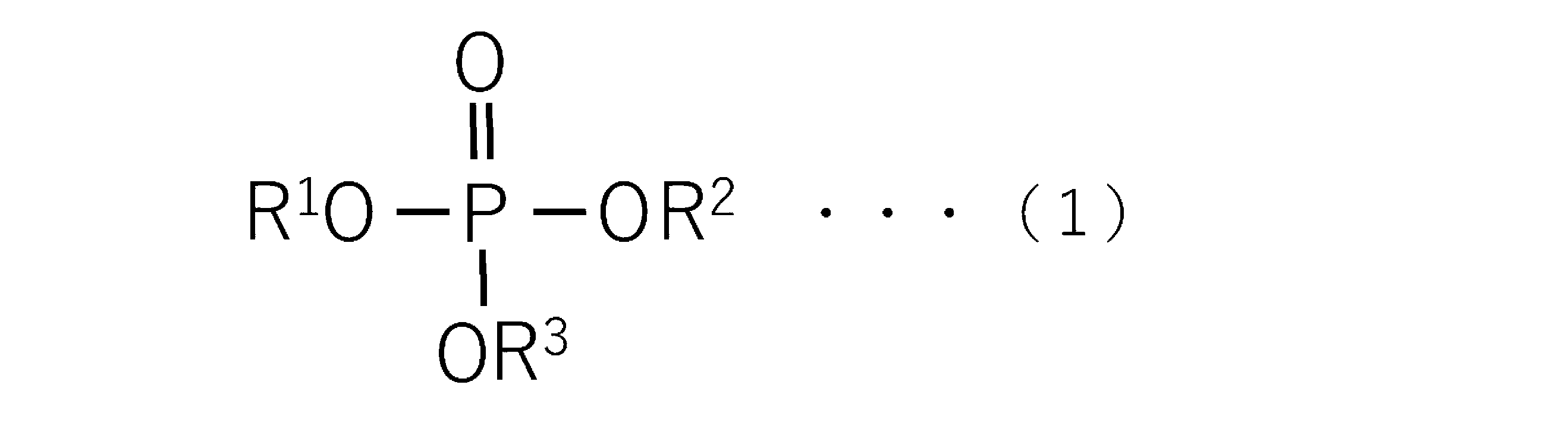
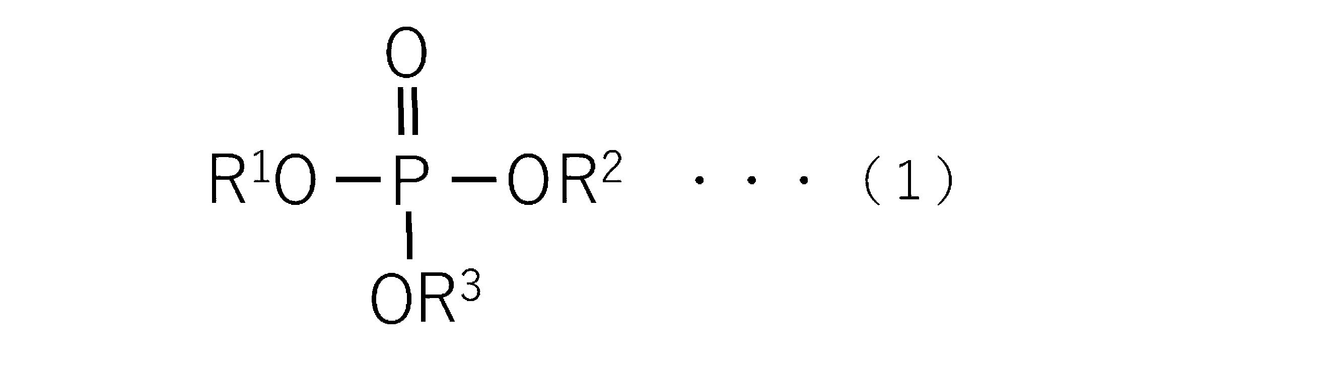
- a conductive paste in a first aspect of the present invention, includes a conductive powder, a ceramic powder, an additive, a resin, and an organic solvent, and contains, as the additive, a phosphoric acid-based additive having a structure shown in the following structural formula (1) in an amount of 0.05 mass% to 1.5 mass% based on the total amount of the conductive paste, the organic solvent includes a terpene-based solvent (a) and one or more solvents (b) selected from a hydrocarbon-based solvent, an acetate-based solvent, an ether-based solvent, and a ketone-based solvent, and the resin includes at least one of a cellulose-based resin and an acetal-based resin.
- the organic solvent includes a terpene-based solvent (a) and one or more solvents (b) selected from a hydrocarbon-based solvent, an acetate-based solvent, an ether-based solvent, and a ketone-based solvent
- the resin includes at least one of a cellulose-based resin and an
- R1 includes at least one of an alkyl group having 6 or more carbon atoms, an ether group having 6 or more carbon atoms, a polyether group, and a polyester group; and R2 and R3 each independently represent a hydrogen atom or an ammonium salt group, or include at least one of an alkyl group, an ether group, and an ester group.
- the conductive powder preferably has an average particle size of 0.05 ⁇ m or more and 1.0 ⁇ m or less.
- the conductive powder preferably contains at least one metal powder selected from Ni, Pd, Pt, Au, Ag, Cu, and alloys thereof.
- the ceramic powder is preferably contained in an amount of 1 mass% or more based on the total amount of the conductive paste.
- the ceramic powder preferably contains barium titanate.
- the ceramic powder preferably has an average particle size of 0.01 ⁇ m or more and 0.5 ⁇ m or less.
- the conductive paste preferably further contains an acid dispersant and/or a base dispersant.
- the conductive paste is preferably for use as an internal electrode of a multilayer ceramic component.
- an electronic component is provided that is formed using the conductive paste.
- the conductive paste of the present invention can reduce the difference in thermal shrinkage of a conductive film manufactured using the conductive paste during firing without requiring any special treatment of the conductive powder.
- the multilayer ceramic capacitor of the present invention can suppress the occurrence of delamination and cracks during firing by forming internal electrodes using the conductive paste.
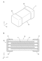
- FIG. 1 is a perspective view and a cross-sectional view showing a multilayer ceramic capacitor according to an embodiment.
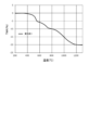
- FIG. 2 is a graph showing the thermal shrinkage curve obtained by thermomechanical analysis (TMA) measurement of Example 1.
- FIG. 3 is a drawing-substitute photograph showing an image of a cross section of the evaluation pellet of Example 1 at 800° C. when fired, taken with a SEM (scanning electron microscope).
- FIG. 4 is a drawing-substitute photograph showing an image of a cross section of the evaluation pellet of Comparative Example 1 when fired at 800° C., taken by SEM.
- the conductive paste according to the embodiment includes a conductive powder, a ceramic powder, an additive, a binder resin, and an organic solvent. Each component will be described in detail below.
- the conductive powder is not particularly limited, and a metal powder can be used, for example, one or more powders selected from Ni, Pd, Pt, Au, Ag, Cu, and alloys thereof.
- a metal powder can be used, for example, one or more powders selected from Ni, Pd, Pt, Au, Ag, Cu, and alloys thereof.
- Ni or its alloy powder (hereinafter, sometimes referred to as "nickel powder") is preferable.
- the Ni alloy for example, an alloy of Ni and at least one element selected from the group consisting of Mn, Cr, Co, Al, Fe, Cu, Zn, Ag, Au, Pt, and Pd can be used.
- the content of Ni in the Ni alloy is, for example, 50 mass% or more, preferably 80 mass% or more.
- the nickel powder may contain about several hundred ppm of element S in order to suppress rapid gas generation due to partial thermal decomposition of the binder resin during the binder removal treatment.
- the manufacturing method is not particularly limited, and it can be manufactured using a conventionally known wet method, dry method, or the like.
- the nickel powder may be nickel powder manufactured by a so-called dry method such as a CVD method, an evaporation quenching method, or a hydrogen reduction method using nickel salt or nickel hydroxide, or it may be nickel powder manufactured by a so-called wet method such as a wet reduction method using a reducing agent such as hydrazine for a nickel salt solution.
- a so-called wet method such as a wet reduction method.
- the nickel powder does not need to have a coating layer as in Patent Document 1.
- the average particle size of the conductive powder is preferably 0.01 ⁇ m or more and 1.0 ⁇ m or less, more preferably 0.01 ⁇ m or more and 0.5 ⁇ m or less, and even more preferably 0.05 ⁇ m or more and 0.4 ⁇ m or less.
- the average particle size of the conductive powder may be, for example, 0.3 ⁇ m or less, 0.25 ⁇ m or less, or 0.2 ⁇ m or less. In the conductive paste of this embodiment, even if the average particle size of the conductive powder is within the above range, the thermal contraction difference during firing can be sufficiently reduced.
- the average particle size is a value determined by observation with a scanning electron microscope (SEM), and is the average value (SEM average particle size, number average) obtained by measuring the particle size of each of multiple particles from an image observed with an SEM at 10,000x magnification.
- SEM scanning electron microscope
- the conductive powder content is preferably 30% by mass or more and less than 70% by mass, and more preferably 40% by mass or more and 60% by mass or less, based on the entire conductive paste.
- the conductive paste has excellent conductivity and dispersibility.
- the ceramic powder is not particularly limited, and for example, in the case of a paste for an internal electrode of a multilayer ceramic capacitor, a known ceramic powder is appropriately selected depending on the type of multilayer ceramic capacitor to be applied.
- a perovskite oxide containing Ba and Ti can be used, and preferably contains barium titanate ( BaTiO3 ).
- the ceramic powder may be a ceramic powder containing barium titanate as a main component and an oxide as a subcomponent.
- the oxide may be an oxide of Mn, Cr, Si, Ca, Ba, Mg, V, W, Ta, Nb, or one or more rare earth elements.
- the ceramic powder may be a perovskite-type oxide ferroelectric ceramic powder in which the Ba and Ti atoms of barium titanate (BaTiO 3 ) are replaced with other atoms, such as Sn, Pb, and Zr.
- the ceramic powder When used as a conductive paste for internal electrodes, the ceramic powder may be a powder of the same composition as the dielectric ceramic powder constituting the green sheet of the multilayer ceramic capacitor (electronic component). This further suppresses the occurrence of cracks due to the difference in thermal contraction at the interface between the dielectric layer and the conductive film in the sintering process.
- such ceramic powders include oxides such as ZnO, ferrite, PZT, BaO, Al 2 O 3 , Bi 2 O 3 , R (rare earth element) 2 O 3 , TiO 2 , and Nd 2 O 3. It is to be noted that one type of ceramic powder may be used, or two or more types may be used.
- the average particle size of the ceramic powder is, for example, 0.01 ⁇ m to 0.5 ⁇ m, and preferably 0.01 ⁇ m to 0.3 ⁇ m.
- the average particle size is a value determined by observation with a scanning electron microscope (SEM), and is the average value (SEM average particle size, number average) obtained by measuring the particle size of each of multiple particles from an image observed with an SEM at a magnification of 50,000 times.
- the content of the ceramic powder is, for example, 1 mass% or more with respect to the entire conductive paste.
- the upper limit of the content of the ceramic powder may be 20 mass% or less, 10 mass% or less, 6 mass% or less, 4 mass% or less, 3 mass% or less, or 2 mass% or less.
- the lower the content of the ceramic powder the better the continuity of the conductive film and the higher the capacitance of the capacitor can be. Even if the content of the ceramic powder is small, the conductive paste of this embodiment can reduce the difference in thermal shrinkage of the conductive film during sintering and reduce the difference in thermal shrinkage behavior with the green sheet.
- the content of the ceramic powder is preferably 2 parts by mass or more per 100 parts by mass of the conductive powder.
- the content of the ceramic powder may be 20 parts by mass or less, 12 parts by mass or less, 8 parts by mass or less, 6 parts by mass or less, or 4 parts by mass or less per 100 parts by mass of the conductive powder.
- the binder resin includes at least one of a cellulose-based resin and an acetal-based resin.
- the paste may include an acetal-based resin, or the acetal-based resin may be used alone.
- the acetal-based resin preferably includes a butyral-based resin, and more preferably includes polyvinyl butyral (PVB).
- PVB polyvinyl butyral
- the content of the acetal resin may be, for example, 20% by mass or more, 40% by mass or more, or 60% by mass or more, based on the total binder resin.
- the content of the acetal resin is within the above range, the adhesion is further improved, and the adhesive strength between the dried film and the green sheet (substrate) is improved.
- the upper limit of the amount of acetal resin is not particularly limited, but may be, for example, 90% by mass or less, 80% by mass or less, or 50% by mass or less of the total binder resin.
- the amount of acetal resin is within the above range, the conductive paste has an appropriate hardness, so that defects such as the printed film not peeling off from the support film and the electrodes being crushed during thermocompression bonding are less likely to occur.
- the weight average molecular weight (Mw) of the acetal resin may be 30,000 or more and 300,000 or less, 50,000 or more and 200,000 or less, or 100,000 or more and 150,000 or less.
- the glass transition point Tg of the acetal resin may be 50°C or more and 90°C or less, or 60°C or more and 80°C or less.
- Cellulose-based resins include, for example, methyl cellulose, ethyl cellulose, ethyl hydroxyethyl cellulose, and nitrocellulose. When a cellulose-based resin is included, it has good solubility in solvents and good decomposition properties when burned. Among cellulose-based resins, ethyl cellulose is preferred.
- the weight average molecular weight (Mw) may be from 10,000 to 300,000, from 30,000 to 250,000, or from 50,000 to 200,000.
- the hydroxyl value of the cellulose-based resin is not particularly limited, but is preferably from 0.1 mgKOH/g to 15 mgKOH/g, more preferably from 0.5 mgKOH/g to 7 mgKOH/g, and even more preferably from 1.5 mgKOH/g to 3 mgKOH/g.
- the cellulose-based resin may be included in one type alone or in two or more types.
- the content of the cellulose-based resin is not particularly limited, but may be, for example, 20% by mass or more, 40% by mass or more, or 60% by mass or more, based on the total content of the binder resin.
- the binder resin contains a cellulose-based resin and an acetal-based resin
- the cellulose-based resin may be contained in an amount of 20% by mass or more, 40% by mass or more, or 60% by mass or more, based on the total content (100% by mass) of the cellulose-based resin and the acetal-based resin.
- the contents of both resins are within the above range, the conductive paste can have a moderate hardness, and defects such as the printed film not peeling off from the support film and the electrodes being crushed during thermocompression are unlikely to occur.
- the thermal shrinkage of the conductive film during firing can be moderated, and the adhesiveness between the conductive film and the green sheet and the dispersibility of the conductive powder can be improved in a balanced manner.
- the upper limit of the content of the cellulose-based resin is not particularly limited, and may be less than 100% by mass, 90% by mass or less, or 80% by mass or less.
- the binder resin may also contain other resins such as acrylic-based resins.
- the binder resin content is preferably 0.5% by mass or more and 10% by mass or less, and more preferably 1% by mass or more and 7% by mass or less, based on the entire conductive paste.
- the binder resin content is within the above range, the conductive paste has excellent conductivity and dispersibility.
- the content of the binder resin is preferably 1 part by mass or more and 20 parts by mass or less, and more preferably 1 part by mass or more and 14 parts by mass or less, per 100 parts by mass of the conductive powder.
- organic solvent a known organic solvent capable of dissolving the binder resin can be used.
- the organic solvent preferably includes a terpene-based solvent (a) and one or more solvents (b) selected from a hydrocarbon-based solvent, an acetate-based solvent, an ether-based solvent, and a ketone-based solvent.
- solvents selected from a hydrocarbon-based solvent, an acetate-based solvent, an ether-based solvent, and a ketone-based solvent.
- Terpene-based solvents (a) include dihydroterpineol, terpineol, dihydroterpinyl acetate, etc., and among these, dihydroterpineol is preferred.
- hydrocarbon solvent (b1) examples include solvents containing tridecane, nonane, cyclohexane, etc., mineral spirits, naphthenic solvents, etc. Among these, it is preferable to contain mineral spirits.
- the content of the hydrocarbon solvent may be 10% by mass or more and 50% by mass or less, or 20% by mass or more and 40% by mass or less, based on the total organic solvent.
- Acetate-based solvents (b2) include isobornyl acetate, isobornyl propionate, isobornyl butyrate, isobornyl isobutyrate, etc.; glycol ether acetates such as ethylene glycol monobutyl ether acetate, diethylene glycol monobutyl ether acetate, diethylene glycol monoethyl ether acetate, dipropylene glycol methyl ether acetate, 3-methoxy-3-methylbutyl acetate, 1-methoxypropyl-2-acetate, etc.; glycol diacetates such as propylene glycol diacetate, 1,4-butanediol diacetate, 1,3-butylene glycol diacetate, 1,6-hexanediol diacetate, etc.; cyclohexanol acetate, etc.
- ether solvent (b3) examples include propylene glycol monoalkyl ethers such as propylene glycol monomethyl ether, propylene glycol monoethyl ether, propylene glycol monopropyl ether, and propylene glycol monobutyl ether; ethylene glycol ethers such as diethylene glycol mono-2-ethylhexyl ether, ethylene glycol mono-2-ethylhexyl ether, diethylene glycol monohexyl ether, and ethylene glycol monohexyl ether; dipropylene glycol methyl-n-propyl ether, dipropylene glycol methyl-n-butyl ether, and dipropylene glycol dimethyl ether.
- propylene glycol monoalkyl ethers such as propylene glycol monomethyl ether, propylene glycol monoethyl ether, propylene glycol monopropyl ether, and propylene glycol monobutyl ether
- Ketone-based solvents (b4) include methyl isobutyl ketone, diisobutyl ketone, etc. When a ketone-based solvent is included, it is possible to adjust the viscosity and improve the drying property without impairing the dispersibility.
- the content of organic solvent is preferably 20% by mass or more and 60% by mass or less, and more preferably 25% by mass or more and 45% by mass or less, based on the total amount of the conductive paste. When the content of organic solvent is within the above range, the conductivity and dispersibility are excellent.
- the content of ether-based solvent is preferably 30% by mass or less.
- the content of the organic solvent is preferably 50 parts by mass or more and 130 parts by mass or less, and more preferably 60 parts by mass or more and 90 parts by mass or less, relative to 100 parts by mass of the conductive powder.
- the conductivity and dispersibility are excellent.
- the organic solvent may include, for example, a terpene-based solvent (a) and a hydrocarbon-based solvent (b1), or may include dihydroterpineol (a) and mineral spirits (b1).
- a terpene-based solvent (a) and a hydrocarbon-based solvent (b1) it is preferable that the terpene-based solvent (a) is contained at 60% by mass to 80% by mass, and the hydrocarbon-based solvent (b1) is contained at 40% by mass to 20% by mass, based on the total amount of organic solvent.
- the organic solvent may contain at least three types of organic solvents, for example, a terpene-based solvent (a), a hydrocarbon-based solvent (b1), and an acetate-based solvent (b2).
- the organic solvent may contain dihydroterpineol (a), mineral spirits (b1), and diethylene glycol monobutyl ether acetate (b2), or may contain dihydroterpineol (a), mineral spirits (b1), and isobornyl acetate (b2).
- these organic solvents are contained, in addition to the above-mentioned effects, the surface smoothness of the dried film is further improved, and the dispersibility of the conductive paste is improved.
- terpene-based solvent (a) is included in an amount of 30% by mass to 70% by mass
- the hydrocarbon-based solvent (b1) is included in an amount of 40% by mass to 20% by mass
- the acetate-based solvent (b2) is included in an amount of 30% by mass to 10% by mass, based on the total amount of organic solvents (100% by mass).
- the conductive paste according to this embodiment contains, as an additive, a phosphate-based additive having a structure represented by the following formula (1).
- R 1 includes at least one of an alkyl group having 6 or more carbon atoms, an ether group having 6 or more carbon atoms, a polyether group, and a polyester group
- R 2 and R 3 each independently represent a hydrogen atom or an ammonium salt group, or include at least one of an alkyl group, an ester group, and an ether group.
- R 1 includes at least one of an alkyl group having 6 or more carbon atoms, an ether group having 6 or more carbon atoms, a polyether group, and a polyester group.
- R 1 preferably includes a polyether group and a polyester group.
- the polyether group include those having an oxyalkylene repeating unit such as oxymethylene, oxyethylene, and oxypropylene.
- the polyether group and the polyester group may have a polyether structure and a polyester structure, and may include other structures.
- the alkyl group and the ether group may each have one or more methylenes substituted with oxygen, and a part of the hydrogen constituting the alkyl group and the ether group may each be substituted with a substituent.
- the polyether group and the polyester group may also have a carbon number of 6 or more.
- R 2 and R 3 are each independently hydrogen or an ammonium base, or contain at least one of an alkyl group, an ester group, and an ether group.
- R 2 and R 3 may be hydrogen.
- the ammonium base may be an alkyl ammonium base.
- the alkyl group, the ester group, and the ether group may have one or more methylenes substituted with oxygen, and a portion of the hydrogen atoms constituting the alkyl group, the ester group, and the ether group may be substituted with a substituent.
- a portion of the hydrogen atoms constituting the alkyl group may be substituted with a phosphate ester group.
- R 2 and R 3 may each independently be hydrogen, an alkyl group, an ammonium base, or an alkyl phosphate ester group.
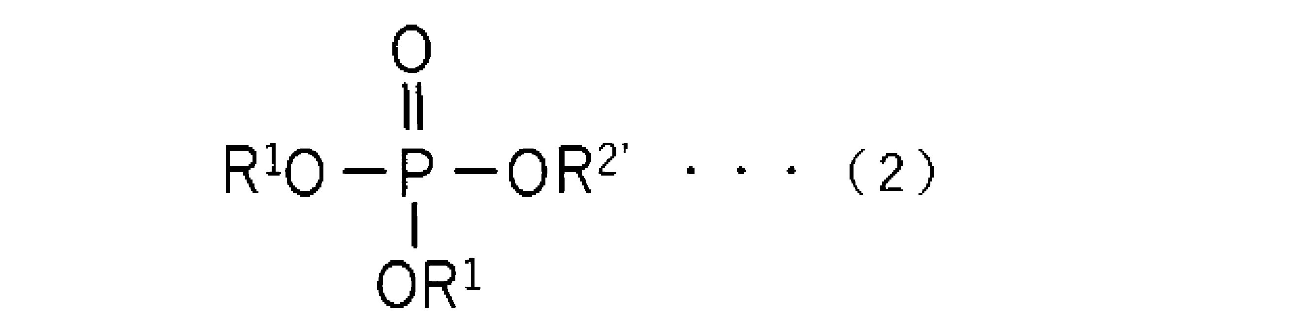
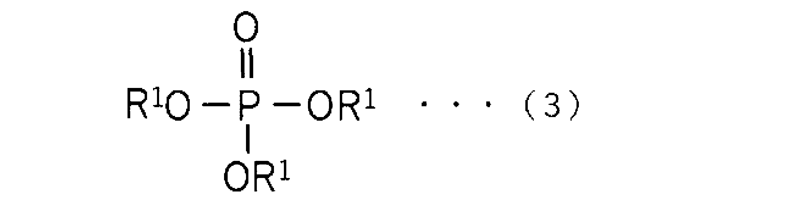
- the additive may also include a phosphoric acid-based additive having one or more structures selected from the following formulas (2) and (3):
- R1 each independently includes at least one of an alkyl group having 6 or more carbon atoms, an ether group having 6 or more carbon atoms, a polyether group, and a polyester group
- R2 ' is a hydrogen atom, an ammonium base, an alkyl group, or an alkyl phosphate ester group.
- the preferred range of R1 in the above formulas (2) and (3) is the same as that of R1 in the above formula (1).
- the conductive paste contains the above phosphoric acid-based additive, when the bonded body of the conductive film and the green sheet is sintered, the difference in thermal contraction of the conductive film is reduced, and the sintering of the conductive film proceeds relatively slowly. The details of why this is the case are unclear, but it is thought that, for example, the phosphoric acid ester inhibits the combustion of the binder resin and forms a carbonized layer, which raises the temperature at which the binder resin completely decomposes.
- the weight average molecular weight of the phosphoric acid additive is preferably 200 or more and 3000 or less. When the molecular weight of the phosphoric acid additive is in the above range, the difference in thermal shrinkage behavior with the green sheet becomes smaller.
- the lower limit of the weight average molecular weight of the phosphoric acid additive may be, for example, 200 or more, 300 or more, 500 or more, or 1000 or more. When the lower limit of the weight average molecular weight of the phosphoric acid additive is in the above range, the thermal shrinkage difference is reduced and dispersibility may be further improved.
- the upper limit of the weight average molecular weight of the phosphoric acid additive may be 2500 or less, 2300 or less, or 2000 or less.
- the content of the phosphoric acid additive is preferably 0.03% by mass or more and 1.5% by mass or less with respect to the entire conductive paste.
- the content of the phosphoric acid additive may be 0.1% by mass or more with respect to the entire conductive paste from the viewpoint of further reducing the difference in thermal shrinkage.
- the content of the phosphoric acid additive is preferably 1% by mass or less with respect to the entire conductive paste, and more preferably 0.8% by mass or less, from the viewpoint of the sinterability of the conductive film and the effect of the decomposition of the additive on thermal shrinkage.
- the content of the phosphoric acid additive may be 0.5% by mass or less, or may be 0.3% by mass or less. If the amount of the phosphoric acid additive is too large, the sintering behavior may be excessively delayed.
- the dispersant may contain, for example, an acid dispersant, a base dispersant, a nonionic dispersant, an amphoteric dispersant, etc., and it is preferable to contain at least one of an acid dispersant and a base dispersant, and it is more preferable to contain an acid dispersant. In addition, it is not necessary to contain a base dispersant. In addition, these dispersants may be used alone or in combination of two or more.
- the acid-based dispersant may include a carboxylic acid-based dispersant such as a higher fatty acid, a polycarboxylic acid-based dispersant, an acid-based dispersant having an acidic group such as a polymer surfactant, and the like, and preferably includes a polycarboxylic acid-based dispersant.
- the polycarboxylic acid-based dispersant may be a comb-shaped carboxylic acid having a comb structure.
- the higher fatty acid may be an unsaturated or saturated carboxylic acid, and is not particularly limited, but examples include stearic acid, oleic acid, myristic acid, palmitic acid, linoleic acid, lauric acid, linolenic acid, and other acids with 11 or more carbon atoms. Of these, oleic acid or stearic acid is preferred.
- Acid dispersants may also be, for example, oleoyl sarcosine, which is a compound of glycine and oleic acid, or alkyl monoamine salt type amide compounds using higher fatty acids such as stearic acid or lauric acid instead of oleic acid.
- oleoyl sarcosine which is a compound of glycine and oleic acid
- alkyl monoamine salt type amide compounds using higher fatty acids such as stearic acid or lauric acid instead of oleic acid.
- a dicarboxylic acid may be included.
- the dicarboxylic acid is a carboxylic acid having two carboxyl groups (COO- groups).
- the average molecular weight of the dicarboxylic acid is not particularly limited, but may be, for example, 200 or more and 1000 or less.
- Basic dispersants include, for example, aliphatic amines such as laurylamine, rosinamine, cetylamine, myristylamine, and stearylamine.
- aliphatic amines such as laurylamine, rosinamine, cetylamine, myristylamine, and stearylamine.
- the dispersant is contained in an amount of, for example, 0.01% by mass or more and 3% by mass or less with respect to the entire conductive paste.
- the upper limit of the dispersant content may be 2% by mass or less, 1% by mass or less, or 0.7% by mass or less.
- the dispersant content is within the above range, the dispersibility of the conductive paste can be improved and sheet attack can be suppressed.
- the dispersant content is high, the difference in thermal contraction behavior with the dielectric increases, but in this embodiment, since a phosphate-based additive is included, even when the dispersant content is high, the difference in thermal contraction of the conductive film during sintering can be reduced and the difference in thermal contraction behavior with the dielectric can be reduced.
- the conductive paste of the present embodiment may contain other additives other than the above components as necessary.
- additives for example, conventionally known additives such as defoamers, plasticizers, surfactants, thickeners, etc. can be used.
- the conductive powder used in the conductive paste has become smaller in particle size, lowering the thermal shrinkage start temperature of the conductive film.
- the conductive paste of this embodiment not only raises the thermal shrinkage start temperature to directly bring the thermal shrinkage behavior of the conductive film closer to that of the green sheet, but also reduces the thermal shrinkage difference of the conductive film in a specific temperature range during sintering, allowing the sintering reaction to proceed slowly and reducing the occurrence of delamination and cracks.
- the conductive paste has the above composition, the sintering of the conductive film proceeds slowly, suppressing the occurrence of delamination and cracks.
- ceramic powder such as barium titanate used in the green sheet has been added to the conductive paste, but in the case of the conductive paste of this embodiment, the amount of ceramic powder added can also be reduced.
- thermomechanical analyzer TMA
- the difference in thermal shrinkage at 600°C to 900°C is preferably 10% or less.
- the thermal shrinkage at a temperature (t°C) means the change rate (%) of the dimension at t°C relative to the dimension (L 0 ) before the start of measurement.
- the difference in thermal shrinkage between any temperatures (t 1 °C to t 2 °C) means the difference between the maximum and minimum values of the thermal shrinkage between temperatures t 1 °C to t 2 °C.
- the conductive paste of the present embodiment can be suitably used in electronic components such as multilayer ceramic capacitors.
- the multilayer ceramic capacitor has, for example, dielectric layers formed using dielectric green sheets and internal electrode layers formed using the conductive paste.
- the firing is performed in a reducing atmosphere to suppress oxidation of the metal used in the conductive film, and the temperature during firing of the laminate is, for example, 1000°C or higher and 1350°C or lower, and the temperature is held for, for example, 0.5 hours or longer and 8 hours or shorter.
- the organic binder in the ceramic green sheet is completely removed, and the ceramic raw powder is fired to form the ceramic dielectric layer 12.
- the organic vehicle in the conductive film is also removed, and the nickel powder or alloy powder mainly composed of nickel is sintered or melted and integrated to form the internal electrode layer 11, forming a multilayer ceramic sintered body in which multiple dielectric layers 12 and internal electrode layers 11 are alternately stacked.
- the sintered multilayer ceramic sintered body may be annealed to incorporate oxygen into the dielectric layer to increase reliability and to suppress reoxidation of the internal electrodes.
- the external electrodes 20 include an external electrode layer 21 and a plating layer 22.
- the external electrode layer 21 is electrically connected to the internal electrode layer 11.
- copper, nickel, or alloys thereof can be suitably used as the material for the external electrodes 20.
- the external electrodes 20 may be provided on the laminate before firing. Note that electronic components other than a laminated ceramic capacitor can also be used.
- the conductive paste was screen-printed on the green sheet.
- a 325 mesh, 1.8 x 1.8 cm pattern screen was used for printing.
- the sheet was dried at 75°C for 10 minutes, and then the back side (green sheet side) was checked with an optical microscope (Eclipse LV100D-U, Nikon Solutions Co., Ltd.) to see if there were any holes or thin layers due to dissolution and swelling in the green sheet. Evaluation was based on the following criteria. ⁇ : No holes or thinning were found in the green sheet. ⁇ : Some holes or thinning was found in the green sheet.
- Binder resin As the binder resin, ethyl cellulose resin (EC) and polyvinyl butyral resin (PVB) were used.
- EC ethyl cellulose resin
- PVB polyvinyl butyral resin
- the dispersant contained in common was an acid dispersant, that is, a polycarboxylic acid dispersant having polyoxyalkylene as a graft chain.
- A-1 A phosphoric acid additive in which, in the compound of formula (1), R 1 contains a polyether group and a polyester group, and R 2 and R 3 contain hydrogen (weight average molecular weight: about 1600).
- A-2 A phosphate additive in which, in the compound of formula (1), R 1 contains a polyether group and a polyester group, and R 2 and R 3 are alkylol ammonium salt groups (weight average molecular weight: about 1,400).
- A-3 A phosphate additive in which, in the compound of formula (1), R 1 includes a polyether group and a polyester group, R 2 is hydrogen, and R 3 is an alkylammonium base (weight average molecular weight: about 1800).
- A-4 A phosphate additive in which, in the compound of formula (1), R 1 contains an ether group having 6 or more carbon atoms, and R 2 and R 3 are hydrogen (weight average molecular weight: about 750).
- Organic Solvent used were dihydroterpineol (DHT), mineral spirits (MSA), and diethylene glycol monobutyl ether acetate (BCA).
- the content of each material in the conductive paste and the evaluation results of the thermal shrinkage behavior are shown in Table 1 and FIG. 2.
- Examples 2 to 14, Comparative Examples 1 to 5 Conductive pastes were prepared and evaluated in the same manner as in Example 1, except that the particle size of the conductive powder, the content of the ceramic powder, the content of the dispersant, the type and content of the additive, the type and content of the binder resin, and the type and content of the organic solvent were set as shown in Tables 1 to 3. The content of each material in the conductive paste and the evaluation results are shown in Tables 1 to 3.
- Table 1 shows the evaluation results of the conductive pastes of Examples 1 to 9 and Comparative Examples 1 to 5, in which the type and content of additives, the type of binder resin, and the type of organic solvent were changed.
- the conductive pastes of Examples 1 to 9 had a smaller difference in thermal contraction at 600°C to 900°C, did not produce lumps or sheet attack, and had a smaller surface roughness, compared to the conductive pastes of Comparative Examples 1 to 3, which do not contain the phosphoric acid-based additive represented by formula (1).
- Comparative Example 4 which contains phosphoric acid as an additive, lumps were produced, and in the case of Comparative Example 5, which contains only terpineol (TPO, a terpene-based solvent) as the organic solvent, sheet attack occurred.
- TPO terpineol
- Example 4 in which the binder resin is only EC
- Example 5 in which the binder resin is only PVB, the above-mentioned difference in thermal shrinkage can be reduced.
- Table 2 shows the evaluation results of the conductive pastes of Examples 1, 9, and 10, in which the content of ceramic powder (BaTiO 3 ) was changed.
- a larger content of ceramic powder can further suppress the thermal shrinkage of the internal electrode layers (compare Example 1 and Example 9 in Table 2).
- Examples 11 and 12 in Table 2 it can be seen that rapid thermal shrinkage can be suppressed even when the content of ceramic powder is reduced.
- Table 3 shows the evaluation results of the conductive pastes of Examples 1, 13, and 14, in which the particle size of the conductive powder (Ni powder) was changed. From Table 3, it can be seen that the larger the particle size of the Ni powder, the smaller the thermal shrinkage difference, but even in Example 14, which has a small particle size, the thermal shrinkage difference was sufficiently reduced.
- the thermal shrinkage curve of the evaluation pellets of Example 1 is shown in Figure 2.
- the thermal shrinkage starting temperature at which the thermal shrinkage rate (dimensional change rate) becomes 5% is relatively low at 550°C.
- the thermal shrinkage curve is upwardly convex, and the thermal shrinkage difference, i.e., the degree of shrinkage, is small.
- the thermal shrinkage curve is generally upwardly convex, and is particularly upwardly convex in the temperature range of 800°C to 900°C, where the thermal shrinkage difference is small.
- Figure 3 shows an image of the cross section of the evaluation pellets of Example 1 taken by a SEM (scanning electron microscope) at 800°C
- Figure 4 shows an image of the cross section of the evaluation pellets of Comparative Example 1 taken by a SEM at 800°C. It was confirmed that the evaluation pellets of Example 1 ( Figure 3) had more voids at 800°C during the firing process and sintering proceeded more slowly than the evaluation pellets of Comparative Example 1 ( Figure 4).
- the conductive paste of the present invention When the conductive paste of the present invention is used to form the internal electrodes of a multilayer ceramic capacitor, a highly reliable multilayer ceramic capacitor can be obtained with high productivity. Therefore, the conductive paste of the present invention can be suitably used for the internal electrodes of multilayer ceramic capacitors, which are chip components in electronic devices such as mobile phones and digital devices that are becoming increasingly miniaturized.
Landscapes
- Engineering & Computer Science (AREA)
- Power Engineering (AREA)
- Chemical & Material Sciences (AREA)
- Microelectronics & Electronic Packaging (AREA)
- Manufacturing & Machinery (AREA)
- Spectroscopy & Molecular Physics (AREA)
- Physics & Mathematics (AREA)
- Dispersion Chemistry (AREA)
- Ceramic Engineering (AREA)
- Inorganic Chemistry (AREA)
- Materials Engineering (AREA)
- Conductive Materials (AREA)
- Ceramic Capacitors (AREA)
- Fixed Capacitors And Capacitor Manufacturing Machines (AREA)
- Compositions Of Macromolecular Compounds (AREA)
Abstract
Description
実施形態の導電性ペーストは、導電性粉末、セラミック粉末、添加剤、バインダー樹脂及び有機溶剤を含む。以下、各成分について詳細に説明する。
導電性粉末としては、特に限定されず、金属粉末を用いることができ、例えば、Ni、Pd、Pt、Au、Ag、Cu、及びこれらの合金から選択される1種以上の粉末を用いることができる。これらの中でも、導電性、耐食性及びコストの観点から、Ni、又はその合金の粉末(以下、「ニッケル粉末」と称する場合がある)が好ましい。Ni合金としては、例えば、Mn、Cr、Co、Al、Fe、Cu、Zn、Ag、Au、Pt及びPdからなる群より選択される少なくとも1種以上の元素とNiとの合金が用いることができる。Ni合金におけるNiの含有量は、例えば、50質量%以上、好ましくは80質量%以上である。また、ニッケル粉末は、脱バインダー処理の際、バインダー樹脂の部分的な熱分解による急激なガス発生を抑制するために、数百ppm程度の元素Sを含んでもよい。
セラミック粉末としては、特に限定されず、例えば、積層セラミックコンデンサの内部電極用ペーストである場合、適用する積層セラミックコンデンサの種類により適宜、公知のセラミック粉末が選択される。セラミック粉末としては、例えば、Ba及びTiを含むペロブスカイト型酸化物を用いることができ、好ましくはチタン酸バリウム(BaTiO3)を含む。
バインダー樹脂としては、セルロース系樹脂及びアセタール系樹脂の少なくとも1種を含む。内部電極用ペーストとして用いる場合、グリーンシートとの接着強度を向上させる観点から、アセタール系樹脂を含む、又は、アセタール系樹脂を単独で使用してもよい。アセタール系樹脂としては、ブチラール系樹脂を含むことが好ましく、ポリビニルブチラール(PVB)を含むことが好ましい。導電性ペーストがアセタール系樹脂を含む場合、グリーンシートとの熱収縮挙動の差をより小さくさせることができる。
有機溶剤としては、バインダー樹脂を溶解することができる公知の有機溶剤を用いることができる。また、有機溶剤は、テルペン系溶剤(a)と、炭化水素系溶剤、アセテート系溶剤、エーテル系溶剤、及びケトン系溶剤から選択される1種以上の溶剤(b)と、を含むことが好ましい。これらの有機溶剤を含むことにより、バインダー樹脂との相溶性に優れ、フィラーの分散性に優れ、かつ、グリーンシートへのシートアタックを抑制できる。
本実施形態に係る導電性ペーストは、添加剤として、下記の式(1)に示される構造を有するリン酸系添加剤を含む。
導電性ペーストが分散剤を含む場合、導電性粉末及びセラミック粉末の分散性を向上することができる。分散剤としては、例えば、酸系分散剤、塩基系分散剤、非イオン系分散剤、両性分散剤等を含んでもよく、酸系分散剤及び塩基系分散剤の少なくとも一方を含むことが好ましく、酸系分散剤を含むことがより好ましい。また、塩基系分散剤を含まなくてもよい。なお、これらの分散剤は、1種又は2種以上を組み合わせて用いてもよい。
本実施形態の導電性ペーストは、必要に応じて、上記の成分以外のその他の添加剤を含んでもよい。その他の添加剤としては、例えば、消泡剤、可塑剤、界面活性剤、増粘剤等の従来公知の添加物を用いることができる。
(a)表面粗さ)
本実施形態に係る導電性ペーストを、基板上にアプリケーターを用いてWet膜厚10μmの厚さに塗布し、120℃で10分間乾燥させて得られた乾燥膜の表面粗さ(Sa)は、0.10μm以下であってもよく、0.07μm以下であってもよく、0.05μm以下であってもよい。なお、乾燥膜の表面粗さSa(算術平均粗さ)は、導電性ペーストの分散性を示す指標の一つでもある。また、表面粗さSaの下限は、特に限定されないが、0を超える値であって小さい値であるほど好ましい。
本実施形態に係る導電性ペーストの製造方法は、特に限定されず、従来公知の方法を用いることができる。導電性ペーストは、例えば、上記の各成分を、3本ロールミル、ボールミル、ミキサー、高圧ホモジナイザー等で攪拌・混練することにより製造することができる。
本発明者は、上記課題を解決するため、鋭意検討を重ねた。その結果、導電性粉末、セラミック粉末、添加剤、樹脂及び有機溶剤を含む導電性ペーストにおいて、特定の組成を有することで、導電性粉末の粒径が小さい場合を含み、該導電性ペーストを用いてなる導電膜の、焼結時の急激な寸法変化を抑える、すなわち、熱収縮差を低減できることを見出し、本発明を完成した。
例えば、本実施形態の導電性ペーストを用いて以下の方法で作製した評価用ペレットについて、熱機械分析装置(thermomechanical analyzer:TMA)を用いて、熱収縮率(寸法変化率)を測定した場合に、600℃以上900℃以下における熱収縮率の差は10%以下であることが好ましい。なお、本明細書において、温度(t℃)における熱収縮率とは、測定開始前の寸法(L0)に対する、t℃における寸法の変化率(%)を意味する。また、任意の温度間(t1℃~t2℃)における熱収縮率の差とは、t1℃~t2℃の温度間における熱収縮率の最大値と最小値の差をいう。
導電性ペーストを、120℃で40分乾燥処理して乾燥導電性シートを得る。得られた乾燥導電性シートを粉砕し、乾燥粉末試料を得る。得られた乾燥粉末試料0.15gを円柱形の金型(底面の直径0.5cm)に入れ、1000kgf/cm2の圧力をかけて、評価用ペレット(直径5mm×厚さ1.5mm)を作製した。
α=100×(L0-L)/L0
L0:測定前の試験片(評価用ペレット)の高さ
L:測定時(温度t℃)における試験片(評価用ペレット)の高さ
また、本実施形態の導電性ペーストを用いて作製した評価用ペレットの焼結開始温度(熱収縮開始温度)は、例えば、500℃以上700℃以下であってもよく、500℃以上650℃以下であってもよい。本実施形態の導電性ペーストは、リン酸系添加剤を含まない以外は同様の条件で作製された導電性ペーストと比較して、比較的高い熱収縮開始温度を有する。また、本実施形態の導電性ペーストは、例えば、焼結開始から900℃程度までの間、熱収縮率(寸法変化率)の変化量を低減させることにより、焼結がゆっくり進行するため、デラミネーション及びクラックの発生が抑制される。なお、熱収縮開始温度は、熱収縮曲線において、熱収縮率が5%になる温度をいう。
本実施形態の導電性ペーストは、積層セラミックコンデンサ等の電子部品に好適に用いることができる。積層セラミックコンデンサは、例えば、誘電体グリーンシートを用いて形成される誘電体層及び導電性ペーストを用いて形成される内部電極層を有する。
次いで、支持フィルムから、グリーンシートを剥離するとともに、グリーンシートとその片面に形成された導電膜とが交互に配置されるように積層した後、加熱・加圧処理により積層体を得る。なお、積層体の両面に、導電性ペーストを塗布していない保護用のセラミックグリーンシートを更に配置する構成としても良い。
(熱収縮挙動の評価)
(i)評価用ペレットの作製
得られた実施例1の導電性ペーストを、120℃で40分乾燥処理し、得られた乾燥導電性シートを粉砕し、乾燥粉末試料を得た。作製した乾燥粉末試料0.15gを円柱形の金型(底面の直径0.5cm)に入れ、1000kgf/cm2の圧力をかけ、評価用ペレットを作製した。
次いで、作製した評価用ペレットを窒素雰囲気下310℃で3時間焼成し、脱バインダー処理を行った。脱バインダーの挙動はTMAにより確認できる。次いで、評価用ペレットを室温に戻し、熱収縮曲線をTMAにより測定した。ここで、試料の装着荷重は10.0g、0.15%の水素を含む窒素ガスと水蒸気ガスをそれぞれガス流量200ml/分の混合ガス雰囲気、昇温度は5℃/分、測定温度範囲は25℃~1300℃とした。測定データより、600℃~900℃における熱収縮率の差を求めた。その評価結果を表1~3に示す。
導電性ペーストの分散性を下記の方法により評価した。
導電性ペーストのシートアタックについては以下のように評価した。「シートアタック」とは、導電性ペーストの成分によりグリーンシートに含有されているバインダー樹脂が溶解して、グリーンシートに穴や皺が生じる現像をいう。
〇:グリーンシートに穴や薄層化が確認できなかった
×:グリーンシートに穴や薄層化が若干確認された
得られた導電性ペーストを、ガラス基板上にアプリケーターを用いてWet膜厚10μmの厚さに塗布し、120℃で10分間乾燥させ、得られた乾燥膜について、レーザー顕微鏡(OLS-5000、株式会社エビデント)を用いて平均表面粗さSa(μm)を測定した。
(導電性粉末)
導電性粉末としては、Ni粉末(SEM平均粒径0.18μm)を使用した。
セラミック粉末としては、チタン酸バリウム(BaTiO3:SEM平均粒径0.05μm)を使用した。
バインダー樹脂としては、エチルセルロース樹脂(EC)、ポリビニルブチラール樹脂(PVB)を使用した。
実施例及び比較例において、共通に含有する分散剤として、酸系分散剤であり、グラフト鎖としてポリオキシアルキレンを有するポリカルボン酸系分散剤を用いた。
リン酸系添加剤として、下記A-1、A-2、A-3、A-4、及びリン酸を用いた。
・A-1:式(1)の化合物において、R1がポリエーテル基及びポリエステル基を含み、R2、R3が水素であるリン酸添加剤を含む(重量平均分子量:約1600)。
・A-2:式(1)の化合物において、R1がポリエーテル基及びポリエステル基を含み、R2、R3がアルキロールアンモニウム塩基であるリン酸添加剤を含む(重量平均分子量:約1400)。
・A-3::式(1)の化合物において、R1がポリエーテル基及びポリエステル基を含み、R2が水素であり、R3がアルキルアンモニウム塩基であるリン酸添加剤を含む(重量平均分子量:約1800)。
・A-4:式(1)の化合物において、R1が炭素数6以上のエーテル基を含み、R2、R3が水素であるリン酸添加剤を含む(重量平均分子量:約750)。
・Z:オレオイルサルコシン
・G:オキシエチレンラウリルアミン
有機溶剤としては、ジヒドロターピネオール(DHT)、ミネラルスピリット(MSA)、及びジエチレングリコールモノブチルエーテルアセテート(BCA)を用いた。
導電性粉末50質量%、セラミック粉末4質量%、分散剤0.15質量%、リン酸系添加剤としての上記「A-1」0.25質量%、バインダー樹脂(EC:PVB=6:4(質量比))3質量%、有機溶剤(DHT:MA=7:3(質量比))42.6質量%を添加して、全体として100質量%となるように配合し、これらの材料を混合して導電性ペーストを作製した。導電性ペーストの各材料の含有量、及び、熱収縮挙動の評価結果を表1及び図2に示す。
導電性粉末の粒径、セラミック粉末の含有量、分散剤の含有量、添加剤の種類及び含有量、バインダー樹脂の種類及び含有量、有機溶剤の種類及び含有量を表1~表3に示されるようにしたこと以外は、実施例1と同様に導電性ペーストを作製し、評価した。導電性ペーストの各材料の含有量、及び、評価結果を表1~表3に示す。
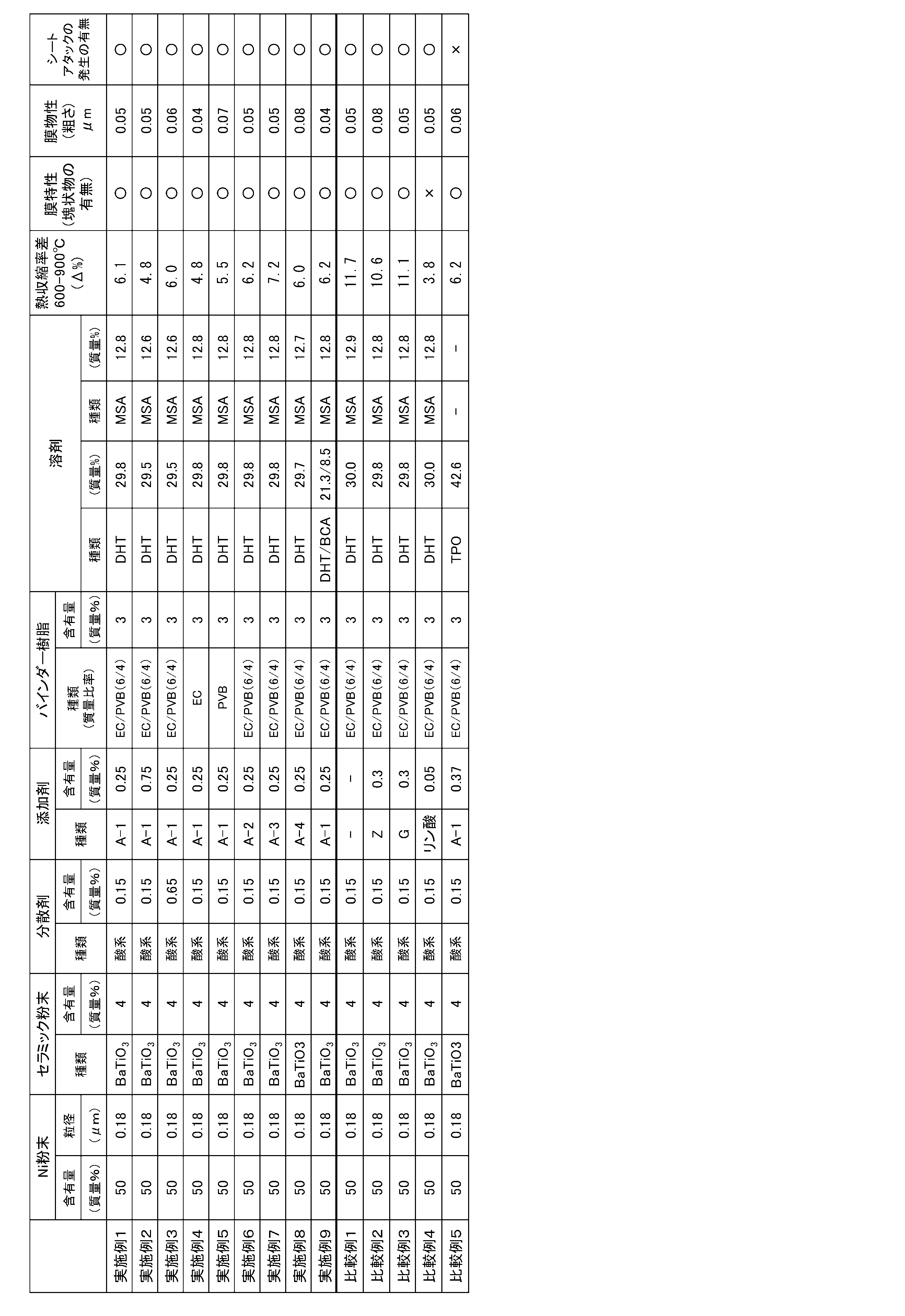
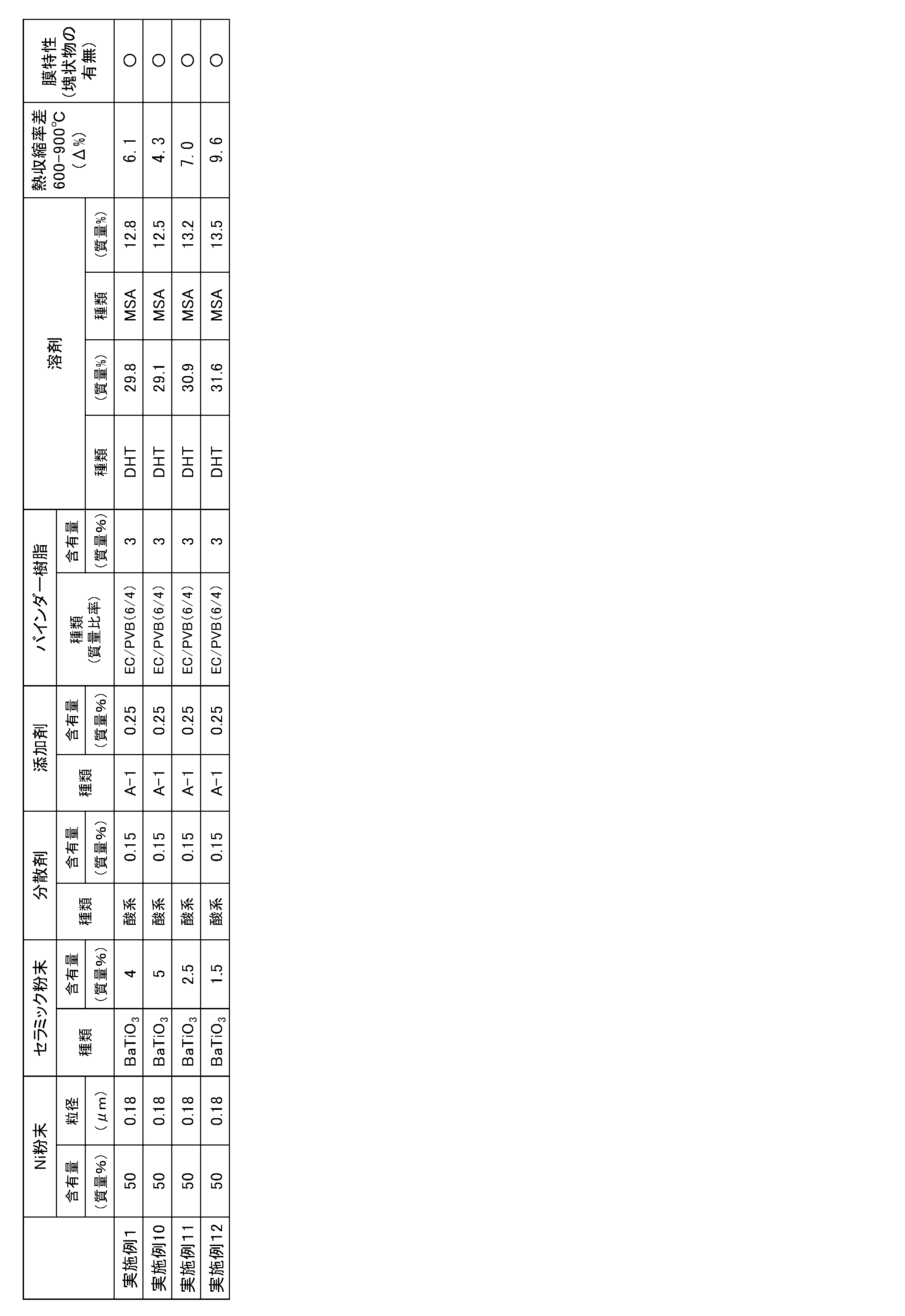
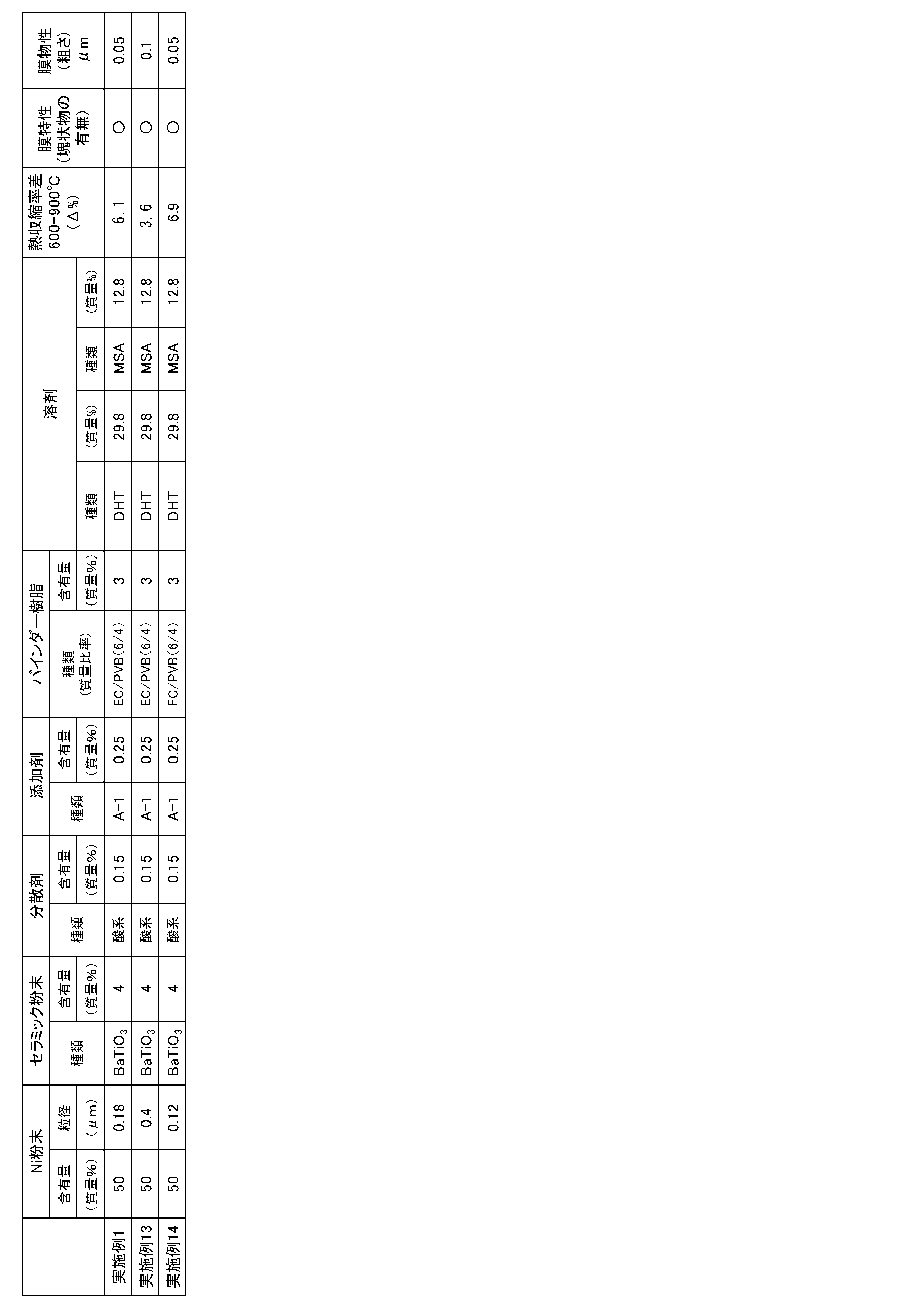
表1は、添加剤の種類及び含有量、バインダー樹脂の種類、有機溶剤の種類をそれぞれ変更した実施例1~9、及び、比較例1~5の導電性ペーストの評価結果を示す。実施例1~9の導電性ペーストは、式(1)で示されるリン酸系添加剤を含まない、比較例1~3の導電性ペーストと比較して、600℃~900℃における熱収縮差が小さく、塊状物及びシートアタックも生じず、表面粗さも小さかった。添加剤としてリン酸を含む比較例4の場合、塊状物が生じ、有機溶剤としてターピネオール(TPO、テルペン系溶剤)のみを含む比較例5の場合、シートアタックが発生した。
10 セラミック積層体
11 内部電極層
12 誘電体層
20 外部電極
21 外部電極層
22 メッキ層
Claims (10)
- 導電性粉末、セラミック粉末、添加剤、バインダー樹脂及び有機溶剤を含む導電性ペーストであって、
前記添加剤として、下記構造式(1)で示される構造を有するリン酸系添加剤を、導電性ペーストの全量に対して0.03質量%以上1.5質量%以下含み、
前記有機溶剤は、テルペン系溶剤(a)と、炭化水素系溶剤、アセテート系溶剤、エーテル系溶剤、及びケトン系溶剤から選択される少なくとも1種の溶剤(b)と、を含み、
前記バインダー樹脂は、セルロース系樹脂、及びアセタール系樹脂のうちの少なくとも1種を含む、導電性ペースト。

- 前記導電性粉末は、平均粒径が0.05μm以上1.0μm以下である、請求項1に記載の導電性ペースト。
- 前記導電性粉末は、Ni、Pd、Pt、Au、Ag、Cu及びこれらの合金から選択される少なくとも1種の金属粉末を含む、請求項1又は2に記載の導電性ペースト。
- 前記セラミック粉末を、導電性ペースト全量に対して1質量%以上含む、請求項1又は2に記載の導電性ペースト。
- 前記セラミック粉末は、チタン酸バリウムを含む、請求項1又は2に記載の導電性ペースト。
- 前記セラミック粉末は、平均粒径が0.01μm以上0.5μm以下である、請求項5に記載の導電性ペースト。
- さらに酸系分散剤又は塩基系分散剤を含む、請求項1又は2に記載の導電性ペースト。
- 積層セラミック部品の内部電極用である、請求項1又は2に記載の導電性ペースト。
- 請求項1又は2に記載の導電性ペーストを用いて形成された、電子部品。
- 誘電体層と内部電極層とを積層した積層体を少なくとも有し、
前記内部電極層は、請求項8に記載の導電性ペーストを用いて形成された、積層セラミックコンデンサ。
Priority Applications (2)
| Application Number | Priority Date | Filing Date | Title |
|---|---|---|---|
| CN202480044925.8A CN121444191A (zh) | 2023-07-04 | 2024-07-02 | 导电性浆料、电子部件以及叠层陶瓷电容器 |
| KR1020257041535A KR20260008816A (ko) | 2023-07-04 | 2024-07-02 | 도전성 페이스트, 전자 부품, 및 적층 세라믹 콘덴서 |
Applications Claiming Priority (2)
| Application Number | Priority Date | Filing Date | Title |
|---|---|---|---|
| JP2023110358A JP2025008310A (ja) | 2023-07-04 | 2023-07-04 | 導電性ペースト、電子部品、及び積層セラミックコンデンサ |
| JP2023-110358 | 2023-07-04 |
Publications (1)
| Publication Number | Publication Date |
|---|---|
| WO2025009525A1 true WO2025009525A1 (ja) | 2025-01-09 |
Family
ID=94171502
Family Applications (1)
| Application Number | Title | Priority Date | Filing Date |
|---|---|---|---|
| PCT/JP2024/023923 Ceased WO2025009525A1 (ja) | 2023-07-04 | 2024-07-02 | 導電性ペースト、電子部品、及び積層セラミックコンデンサ |
Country Status (5)
| Country | Link |
|---|---|
| JP (1) | JP2025008310A (ja) |
| KR (1) | KR20260008816A (ja) |
| CN (1) | CN121444191A (ja) |
| TW (1) | TW202510984A (ja) |
| WO (1) | WO2025009525A1 (ja) |
Citations (2)
| Publication number | Priority date | Publication date | Assignee | Title |
|---|---|---|---|---|
| WO2020166361A1 (ja) * | 2019-02-12 | 2020-08-20 | 住友金属鉱山株式会社 | 導電性ペースト、電子部品及び積層セラミックコンデンサ |
| JP2022148195A (ja) * | 2021-03-24 | 2022-10-06 | 住友金属鉱山株式会社 | ニッケル粒子の表面処理方法およびニッケル粉末の製造方法 |
Family Cites Families (2)
| Publication number | Priority date | Publication date | Assignee | Title |
|---|---|---|---|---|
| JP6042736B2 (ja) | 2013-01-30 | 2016-12-14 | 新日鉄住金化学株式会社 | ニッケル微粒子含有組成物及びその製造方法 |
| JP5978371B2 (ja) | 2015-09-10 | 2016-08-24 | 株式会社ノリタケカンパニーリミテド | コアシェル粒子及び導体形成用組成物 |
-
2023
- 2023-07-04 JP JP2023110358A patent/JP2025008310A/ja active Pending
-
2024
- 2024-07-02 WO PCT/JP2024/023923 patent/WO2025009525A1/ja not_active Ceased
- 2024-07-02 CN CN202480044925.8A patent/CN121444191A/zh active Pending
- 2024-07-02 KR KR1020257041535A patent/KR20260008816A/ko active Pending
- 2024-07-03 TW TW113124954A patent/TW202510984A/zh unknown
Patent Citations (2)
| Publication number | Priority date | Publication date | Assignee | Title |
|---|---|---|---|---|
| WO2020166361A1 (ja) * | 2019-02-12 | 2020-08-20 | 住友金属鉱山株式会社 | 導電性ペースト、電子部品及び積層セラミックコンデンサ |
| JP2022148195A (ja) * | 2021-03-24 | 2022-10-06 | 住友金属鉱山株式会社 | ニッケル粒子の表面処理方法およびニッケル粉末の製造方法 |
Also Published As
| Publication number | Publication date |
|---|---|
| JP2025008310A (ja) | 2025-01-20 |
| CN121444191A (zh) | 2026-01-30 |
| KR20260008816A (ko) | 2026-01-16 |
| TW202510984A (zh) | 2025-03-16 |
Similar Documents
| Publication | Publication Date | Title |
|---|---|---|
| JP7498896B2 (ja) | 導電性ペースト、電子部品、及び積層セラミックコンデンサ | |
| JP7750318B2 (ja) | 導電性ペースト、電子部品、及び積層セラミックコンデンサ | |
| TWI814910B (zh) | 導電性漿料、電子零件、及積層陶瓷電容器 | |
| WO2020137289A1 (ja) | 導電性ペースト、電子部品、及び積層セラミックコンデンサ | |
| TWI801445B (zh) | 導電性漿料、電子零件以及層積陶瓷電容器 | |
| CN116113671A (zh) | 凹版印刷用导电性浆料、电子部件以及叠层陶瓷电容器 | |
| JP7517156B2 (ja) | 導電性ペースト、電子部品及び積層セラミックコンデンサ | |
| JP2025081376A (ja) | 導電性ペースト、電子部品及び積層セラミックコンデンサ | |
| CN112470236B (zh) | 导电性浆料、电子部件以及叠层陶瓷电容器 | |
| TW202414441A (zh) | 導電性漿料、乾燥膜、內部電極、及積層陶瓷電容器 | |
| JP2025008310A (ja) | 導電性ペースト、電子部品、及び積層セラミックコンデンサ | |
| KR102832932B1 (ko) | 그라비아 인쇄용 도전성 페이스트, 전자 부품, 및 적층 세라믹 콘덴서 | |
| TW202313866A (zh) | 凹版印刷用導電性漿料、電子零件、及積層陶瓷電容器 | |
| JP7648002B2 (ja) | 導電性ペースト、電子部品、及び積層セラミックコンデンサ | |
| JP7648001B2 (ja) | 導電性ペースト、電子部品、及び積層セラミックコンデンサ | |
| JP7586088B2 (ja) | 導電性組成物、導電性ペースト、電子部品、及び積層セラミックコンデンサ | |
| JP2024146128A (ja) | 導電性ペースト、電子部品、及び、積層セラミックコンデンサ | |
| JP2024146126A (ja) | 導電性ペースト、電子部品、及び、積層セラミックコンデンサ | |
| JP2026068235A (ja) | 導電性ペースト、電子部品、並びに、積層セラミックコンデンサ | |
| WO2025249550A1 (ja) | 導電性ペースト、電子部品、及び積層セラミックコンデンサ | |
| JP2023072900A (ja) | 導電性ペーストおよびその製造方法 |
Legal Events
| Date | Code | Title | Description |
|---|---|---|---|
| 121 | Ep: the epo has been informed by wipo that ep was designated in this application |
Ref document number: 24836038 Country of ref document: EP Kind code of ref document: A1 |
|
| ENP | Entry into the national phase |
Ref document number: 1020257041535 Country of ref document: KR Free format text: ST27 STATUS EVENT CODE: A-0-1-A10-A15-NAP-PA0105 (AS PROVIDED BY THE NATIONAL OFFICE) |
|
| WWE | Wipo information: entry into national phase |
Ref document number: 1020257041535 Country of ref document: KR |
|
| WWP | Wipo information: published in national office |
Ref document number: 1020257041535 Country of ref document: KR |
|
| NENP | Non-entry into the national phase |
Ref country code: DE |
|
| 122 | Ep: pct application non-entry in european phase |
Ref document number: 24836038 Country of ref document: EP Kind code of ref document: A1 |