WO2025009336A1 - 横熱電効果を用いた垂直型熱電変換素子、及び垂直型熱電変換素子の評価方法 - Google Patents
横熱電効果を用いた垂直型熱電変換素子、及び垂直型熱電変換素子の評価方法 Download PDFInfo
- Publication number
- WO2025009336A1 WO2025009336A1 PCT/JP2024/021055 JP2024021055W WO2025009336A1 WO 2025009336 A1 WO2025009336 A1 WO 2025009336A1 JP 2024021055 W JP2024021055 W JP 2024021055W WO 2025009336 A1 WO2025009336 A1 WO 2025009336A1
- Authority
- WO
- WIPO (PCT)
- Prior art keywords
- thermoelectric
- layer
- conversion element
- vertical
- thickness
- Prior art date
- Legal status (The legal status is an assumption and is not a legal conclusion. Google has not performed a legal analysis and makes no representation as to the accuracy of the status listed.)
- Ceased
Links
Images


Classifications
-
- H—ELECTRICITY
- H02—GENERATION; CONVERSION OR DISTRIBUTION OF ELECTRIC POWER
- H02N—ELECTRIC MACHINES NOT OTHERWISE PROVIDED FOR
- H02N11/00—Generators or motors not provided for elsewhere; Alleged perpetua mobilia obtained by electric or magnetic means
-
- H—ELECTRICITY
- H10—SEMICONDUCTOR DEVICES; ELECTRIC SOLID-STATE DEVICES NOT OTHERWISE PROVIDED FOR
- H10N—ELECTRIC SOLID-STATE DEVICES NOT OTHERWISE PROVIDED FOR
- H10N15/00—Thermoelectric devices without a junction of dissimilar materials; Thermomagnetic devices, e.g. using the Nernst-Ettingshausen effect
- H10N15/20—Thermomagnetic devices using thermal change of the magnetic permeability, e.g. working above and below the Curie point
Definitions
- the present invention relates to a vertical thermoelectric conversion element that uses the lateral thermoelectric effect, and a method for evaluating a vertical thermoelectric conversion element.
- the Seebeck effect a common thermoelectric effect, is a phenomenon in which an electric field is generated parallel to a temperature gradient ⁇ T when a conductive material is subjected to a temperature gradient ⁇ T.
- Thermoelectric power generation modules and heat flow sensors that use this effect have already been commercialized and are available on the market, but their applications are limited due to various issues, such as their complex structure, difficulty in making them large-area, low durability and flexibility, and high cost.
- thermoelectric generation module in which an electric field is generated in a direction perpendicular to ⁇ T, it is possible to function as a thermoelectric generation module or heat flow sensor with an extremely simple in-plane connection type structure, and it is hoped that a new thermoelectric generation laminate that solves the above-mentioned problems will be created (Patent Document 1, Non-Patent Document 1).
- thermoelectric power of the anomalous Nernst effect of magnetic materials reported to date at room temperature is less than 10 ⁇ V/K (Non-Patent Document 2), and there is active research into materials with greater transverse thermoelectric power.
- the inventors have proposed a vertical thermoelectric conversion element with a layered structure consisting of a magnetic material, a thermoelectric material, and an insulating material sandwiched between the two, and have demonstrated that a high transverse thermoelectric power can be obtained by converting the Seebeck current of the thermoelectric material into a direction perpendicular to ⁇ T due to the anomalous Hall effect of the magnetic material (Patent Document 2, Non-Patent Documents 3 and 4).
- thermoelectric power due to the anomalous Nernst effect is still small compared to the Seebeck effect of thermoelectric materials, and it is necessary to realize a higher transverse thermoelectric power for practical applications.
- a high transverse thermoelectric power can be obtained in the vertical thermoelectric conversion element made of the above-mentioned magnetic material and thermoelectric material, it is necessary to create a closed circuit structure in which the magnetic material and the thermoelectric material are electrically conductive only on the high temperature side and the low temperature side of ⁇ T, and are electrically insulated in other parts. Therefore, there is a problem that the end conductor parts and insulating layers required for the closed circuit complicate the structure of the thermoelectric conversion element, hindering miniaturization and modularization.
- connection positions of the output terminals are limited to both ends of the magnetic layer in the direction of generating electric potential, which makes the connection of the output terminals complicated. Also, if the connection positions of the output terminals extend to the thermoelectric layer laminated on the magnetic layer, the voltage generated by the thermoelectric power is lowered compared to the case where the output terminals are connected only to the magnetic layer.
- the present invention has been made to solve the problems of the conventional technology described above, and aims to provide a vertical thermoelectric conversion element that uses the lateral thermoelectric effect and has a laminated structure in which the magnetic material and the thermoelectric material are in direct electrical contact, without requiring end conductor portions and insulating layers.
- Another object of the present invention is to provide a method for evaluating a vertical thermoelectric conversion element that is suitable for use in material search and optimization design of a vertical thermoelectric conversion element using the lateral thermoelectric effect.
- the vertical thermoelectric conversion element of the present invention comprises a thermoelectric layer 10 made of a thermoelectric material exhibiting the Seebeck effect, one end of the thermoelectric layer 10 being a low-temperature side and the other end opposite the low-temperature side being a high-temperature side, and a magnetic layer 20 laminated on the thermoelectric layer 10, the magnetic layer 20 having a magnetization component, an external magnetic field, or a magnetization component and an external magnetic field in the film thickness direction of the magnetic layer 20, being electrically conductive, and having a temperature gradient direction of the magnetic layer 20 and a temperature gradient direction of the magnetic layer 20.
- thermoelectric layer 10 the magnetic layer 20, or the thermoelectric layer 10 and the magnetic layer 20 for extracting the potential generated in the cross product direction, which is the temperature gradient direction of the thermoelectric layer 10, and the magnetization direction of the magnetic layer 20, the external magnetic field direction, or the cross product direction of the magnetization direction and the external magnetic field direction.
- the ratio (x) of the thickness (L z TE ) of the thermoelectric layer 10 to the sum of the thickness (L z TE ) of the thermoelectric layer 10 and the thickness (L z M ) of the magnetic layer 20 has a lower limit value of 0.2 less than the x value that maximizes the transverse thermoelectric power (S y tot ) and an upper limit value of 0.2 more than the x value, and when the lower limit value is negative, the lower limit value is zero, and when the upper limit value exceeds 1, the upper limit value is 1.
- the transverse thermoelectric power (S y tot ) is preferably formulated by the following equation:
- the magnetic material of the magnetic layer is Fe x Ga 1-x (0.5 ⁇ x ⁇ 0.9)
- the thermoelectric material of the thermoelectric layer is n-type Si
- the ratio of the thickness (L z TE ) of the thermoelectric layer to the sum of the thickness (L z TE ) of the thermoelectric layer and the thickness (L z M ) of the magnetic layer is: 0.98 ⁇ LzTE /( LzTE + LzM ) ⁇ 0.9995
- the transverse thermoelectric power S y tot is 6.8 ( ⁇ V/K) or more, which is more than twice the transverse thermoelectric power due to the anomalous Nernst effect of Fe 70 Ga 30 , which is the magnetic material.
- the magnetic material of the magnetic layer is Fe x Ga 1-x (0.5 ⁇ x ⁇ 0.9)
- the thermoelectric material of the thermoelectric layer is n-type Si
- the ratio of the thickness (L z TE ) of the thermoelectric layer to the sum of the thickness (L z TE ) of the thermoelectric layer and the thickness (L z M ) of the magnetic layer is: 0.99 ⁇ LzTE /( LzTE + LzM ) ⁇ 0.999
- the transverse thermoelectric power S y tot is 10 ( ⁇ V/K) or more, which is four times or more the transverse thermoelectric power due to the anomalous Nernst effect of Fe 70 Ga 30 which is the magnetic material.
- the magnetic material of the magnetic layer is Fe x Ga 1-x (0.5 ⁇ x ⁇ 0.9)
- the thermoelectric material of the thermoelectric layer is n-type Si
- the ratio of the thickness (L z TE ) of the thermoelectric layer to the sum of the thickness (L z TE ) of the thermoelectric layer and the thickness (L z M ) of the magnetic layer is: 0.994 ⁇ LzTE / ( LzTE + LzM ) ⁇ 0.998
- the transverse thermoelectric power S y tot is 12.5 ( ⁇ V/K) or more, which is five times or more the transverse thermoelectric power due to the anomalous Nernst effect of Fe 70 Ga 30 which is a magnetic material.
- the magnetic material of the magnetic layer is one type of magnetic material selected from the following group (A) to (H): (A) one or more L10 type ordered alloys selected from the group consisting of FePt, CoPt, FePd, CoPd, FeNi, MnAl, and MnGa; (B) one or two Heusler alloys selected from the group consisting of Co 2 MnGa and Co 2 MnAl; (C) one or more kinds of D022 type ordered alloys selected from the group consisting of Mn3Ga , Mn2FeGa , Mn2CoGa , and Mn2RuGa ; (D) one or more alloys selected from the group consisting of FeCr, FeAl, FeGa, FeSi, FeTa, FeIr, FePt, FeSn, FeSm, FeTb, CoFeB, CoTb, and NiPt; (E) one or more L10 type ordered alloys selected from the group consisting of FePt
- the FeGa may preferably be Fe x Ga 1-x (0.5 ⁇ x ⁇ 0.9).
- the thermoelectric material of the thermoelectric layer is preferably one type of thermoelectric material selected from the group of thermoelectric materials consisting of Bi2Te3 , PbTe, Si, Ge, FeSi alloy, CrSi alloy, MgSi alloy, CoSb3 alloy, Fe2VAl -based Heusler alloy, and SrTiO3 .
- the Bi 2 Te 3 , PbTe, Si, or Ge is doped with a p-type or n-type element to a carrier concentration of 0.1 ⁇ 10 19 to 3 ⁇ 10 19 cm -3 .
- the Si is p-type Si
- the sign of the transverse thermoelectric power is opposite to that of n-type Si.
- the magnetic layer is a single layer or multiple layers, and the thermoelectric layer is a single layer in electrical contact with the magnetic layer, or multiple layers sandwiching the magnetic layer.
- the method for evaluating a vertical thermoelectric conversion element of the present invention is a method for evaluating a vertical thermoelectric conversion element according to any one of the vertical thermoelectric conversion elements [1] to [10], wherein, in the following formula, Based on the resistivity and Seebeck coefficient of the thermoelectric material, and the resistivity, Seebeck coefficient, anomalous Hall resistivity, and anomalous Nernst coefficient of the magnetic material, the ratio (x) of the thickness of the thermoelectric layer (L z TE ) to the sum of the thickness of the thermoelectric layer (L z TE ) and the thickness of the magnetic layer (L z M ) is determined so as to maximize the transverse thermoelectric power (S y tot ).
- the symbols are defined as follows: [13] In the evaluation method [12] for a vertical thermoelectric conversion element of the present invention, it is preferable to further define the range of this ratio (x) so that the lower limit is a value obtained by subtracting 0.2 from the value that maximizes the transverse thermoelectric power (S y tot ) and the upper limit is a value obtained by adding 0.2 to the value, and the lower limit is zero when the lower limit is negative, and the upper limit is 1 when the upper limit exceeds 1. [14] In the evaluation method [12] of the vertical thermoelectric conversion element of the present invention, it is preferable to determine the transverse thermoelectric power output coefficient (PF) defined by the following equation so as to maximize it.
- PF transverse thermoelectric power output coefficient
- the effective resistivity ( ⁇ eff ) in the plane (xy plane) of the vertical thermoelectric conversion element is defined by the following formula: [15]
- the evaluation method [14] of the vertical thermoelectric conversion element of the present invention it is preferable to determine the evaluation method so as to maximize an isothermal dimensionless figure of merit (zT) representing the efficiency of the transverse thermoelectric effect defined by the following equation.
- the effective thermal conductivity (k eff ) in the plane (xy plane) of the vertical thermoelectric conversion element is defined by the following formula:
- the output terminals may be connected to both ends of the magnetic layer in the electric potential generating direction, as well as to the thermoelectric layer laminated on the magnetic layer, which has the effect of facilitating the connection of the output terminals. Also, even if the output terminals are connected to the thermoelectric layer laminated on the magnetic layer, the decrease in voltage generated by the thermoelectric power remains within an acceptable range, compared to the case where the output terminals are connected only to the magnetic layer.
- the vertical thermoelectric conversion element of the present invention in a two-layer structure including a magnetic layer made of a magnetic material that has a magnetization component or an external magnetic field in the film thickness direction and is conductive and generates a potential in the temperature gradient direction of the magnetic layer, as well as in the direction of the magnetization direction, the external magnetic field, or the cross product direction of the magnetization direction and the external magnetic field, and a thermoelectric layer made of a thermoelectric material exhibiting the Seebeck effect, or in a structure in which a sandwich structure of a magnetic layer and a thermoelectric layer is laminated in multiple layers, the ratio of the thickness of the thermoelectric layer (L z TE ) to the sum of the thickness of the thermoelectric layer (L z TE ) and the thickness of the magnetic layer (L z M ) is preferably set to a lower limit value obtained by subtracting 0.2 from the value that maximizes the transverse thermoelectric power (S y tot ) and an upper limit value obtained by adding 0.2 to the value, thereby
- thermoelectric layer thickness LzTE
- LzM the magnetic layer thickness
- zT isothermal dimensionless figure of merit
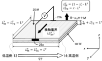
- FIG. 2 is an explanatory diagram of a vertical thermoelectric conversion element according to one embodiment of the present invention, showing the transverse thermoelectric effect in a two-layer structure of magnetic material and thermoelectric material, the dimensions of the materials, and the ratio (x) of the thermoelectric layer thicknesses.
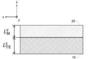
- FIG. 2 is an explanatory diagram of a vertical thermoelectric conversion element according to one embodiment of the present invention, showing a two-layer structure of a magnetic material and a thermoelectric material.
- FIG. 2 is an explanatory diagram of a vertical thermoelectric conversion element according to one embodiment of the present invention, showing a cross-sectional view of a laminated structure in which magnetic materials and thermoelectric materials are multi-layered.
- FIG. 2 is a structural diagram of a sample used in the examples.
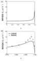
- thermoelectric layer thickness x
- vertical axis the transverse thermoelectric power S y tot ( ⁇ V/K).
- A) is an enlarged view of the entire range of 0 ⁇ x ⁇ 1
- B) is an enlarged view of 0.97 ⁇ x ⁇ 1.00.
- Fig. 1 is an explanatory diagram of the main part of a vertical thermoelectric conversion element showing one embodiment of the present invention, and is a perspective view showing a two-layer structure of a magnetic material and a thermoelectric material.
- the left-right direction is the x-axis
- the diagonal direction in the front-back direction is the y-axis
- the up-down direction is the z-axis.
- the transverse thermoelectric power (S y tot ) is expressed by the following formula (1).
- the ratio (x) of the thickness of the thermoelectric layer (L z TE ) to the sum of the thickness of the thermoelectric layer (L z TE ) and the thickness of the magnetic layer (L z M ) is determined so as to maximize the transverse thermoelectric power (S y tot ) based on the resistivity and Seebeck coefficient of the thermoelectric material, and the resistivity, Seebeck coefficient, anomalous Hall resistivity, and anomalous Nernst coefficient of the magnetic material. Furthermore, it is advisable to determine the allowable range of the ratio (x) taking into consideration the manufacturing yield.
- the ratio (x) of the thermoelectric layer thickness (L z TE ) to the sum of the thermoelectric layer thickness (L z TE ) and the magnetic layer thickness (L z M ) is set to a range in which the lower limit is a value obtained by subtracting 0.2 from the value that maximizes the transverse thermoelectric power (S y tot ) and the upper limit is a value obtained by adding 0.2 thereto, and the lower limit is set to zero if the lower limit is negative, and the upper limit is set to 1 if the upper limit exceeds 1.
- the ratio (x) of the thermoelectric layer thickness (L z TE ) to the sum of the thermoelectric layer thickness (L z TE ) and the magnetic layer thickness (L z M ) may have a lower limit value of 0.1 less than the value that maximizes the transverse thermoelectric power (S y tot ) and an upper limit value of 0.1 more than that, or may have a lower limit value of 0.05 less than the value that maximizes the transverse thermoelectric power (S y tot ) and an upper limit value of 0.05 more than that.
- the dimensions of the material, length Lx in the x-axis direction, width Ly in the y-axis direction, and thickness Lz in the z-axis direction, are expressed by the following formulas (2) to (4).
- the thickness LzM of the magnetic material M and the thickness LzTE of the thermoelectric material TE are expressed by the following formulas (5) and (6).
- the vertical thermoelectric conversion element of the present invention has a two-layer structure of a thermoelectric material layer (thermoelectric layer) TE10 and a magnetic material layer (magnetic layer) M20, and is equipped with output terminals 26a and 26b.
- B indicates the magnetic field direction of the magnetic flux density
- ⁇ T indicates the direction of the temperature gradient from the low temperature side to the high temperature side.
- the magnetic flux density B is expressed by the following formula using the magnetization M, the external magnetic field H, and the magnetic permeability ⁇ 0 .
- B ⁇ 0 H+M (7)
- the thermoelectric material layer TE10 is made of a thermoelectric material having the Seebeck effect, and one end of the thermoelectric material layer TE10 is a low-temperature end 12, and the other end opposite the low-temperature end 12 is a high-temperature end 14.
- electric heating, exhaust heat steam from a boiler device, or high-temperature wastewater can be used to heat the high-temperature end 14.
- air cooling or water cooling can be used to cool the low-temperature end 12, or a solid heat dissipation member can be attached.
- thermoelectric materials having the Seebeck effect include Bi 2 Te 3 , PbTe, Si, Ge, FeSi alloy, CrSi alloy, MgSi alloy, CoSb 3 alloy, Fe 2 VAl-based Heusler alloy, and SrTiO 3.
- Bi 2 Te 3 , PbTe, Si, and Ge In order to adjust the resistivity and thermoelectric figure of merit Z, it is advisable to dope Bi 2 Te 3 , PbTe, Si, and Ge with a p-type or n-type element doping concentration of 0.1x10 19 to 3x10 19 cm -3 .
- the magnetic material layer M20 is a magnetic material layer M laminated on the thermoelectric material layer TE10, and is magnetized or/and an external magnetic field is applied in the thickness direction of the magnetic material layer M20, and is conductive, generating a potential in the cross product direction of the temperature gradient direction ⁇ T of the magnetic material layer M20 and the magnetization direction M.
- the magnetic material layer M20 is preferably made of a magnetic material having conductivity and an anomalous Hall angle of 1% or more. A magnetic material will exhibit both the anomalous Nernst effect and the anomalous Hall effect, but in order to obtain a large assist effect, it is preferable to select a magnetic material that exhibits a large anomalous Hall effect (anomalous Hall angle).
- the anomalous Hall angle is a parameter that indicates the degree to which a current is bent laterally when it is passed through a magnetic material. If the anomalous Hall angle is less than 1%, the potential generated by the cross product direction of the temperature gradient direction ⁇ T of the magnetic material layer M and the magnetization direction M is low, which is not preferable for a vertical thermoelectric conversion element. In addition, since it is necessary for the material to have spontaneous magnetization at room temperature or higher in practical use, it is preferable for the material to have spontaneous magnetization up to 100°C or higher. Furthermore, there are three types of cases where magnetization in the film thickness direction of the magnetic material layer M and/or an external magnetic field is applied. The first type is the magnetization direction when only magnetization occurs and no external magnetic field is applied. The second type is the external magnetic field direction when only an external magnetic field is applied and no magnetization occurs. The third type is the combined magnetic field direction of the magnetization direction and the external magnetic field direction when both magnetization and an external magnetic field are applied.
- Such magnetic materials having an anomalous Hall angle of 1% or more and spontaneous magnetization up to 100° C. or more include one type of magnetic material selected from the group consisting of L1 0 type ordered alloys, Heusler alloys, D0 22 type ordered alloys, binary disordered alloys, permanent magnet materials, multilayer magnetic materials, perovskite nitride materials, and D0 19 type ordered alloys. That is, examples of L1 0 type ordered alloys include FePt, CoPt, FePd, CoPd, FeNi, MnAl, and MnGa. Examples of Heusler alloys include Co 2 MnGa and Co 2 MnAl.
- Examples of D0 22 type ordered alloys include Mn 3 Ga, Mn 2 FeGa, Mn 2 CoGa, and Mn 2 RuGa.
- Examples of binary disordered alloys include FeCr, FeAl, FeGa, FeSi, FeTa, FeIr, FePt, FeSn, FeSm, FeTb, CoFeB, CoTb, and NiPt.
- Examples of permanent magnet materials include SmCo5- based magnets, Sm2Co17 - based magnets, and Nd2Fe14B -based magnets.
- Examples of multilayer magnetic materials include Co/Pt and Co/Pd.
- Examples of perovskite nitride materials include Mn4N and Fe4N .
- Examples of D019- type ordered alloys include Mn3Ga , Mn3Ge , and Mn3Sn .
- the output terminals 26a and 26b are output terminals for extracting the electric potential generated in the cross product direction, which is the cross product direction of the temperature gradient direction ⁇ T of the thermoelectric material layer TE and the magnetization direction M of the magnetic material layer M, and are provided at both ends of the cross product direction of the magnetic material layer M.
- a temperature gradient ⁇ T exists in the length x-axis direction, and when magnetization or an external magnetic field is applied in the thickness z-axis direction, a transverse thermal electric field E y tot is generated in the width y-axis direction.
- FIG. 2A is a cross-sectional view or a front view in an xz plane of a vertical thermoelectric conversion element showing one embodiment of the present invention, and shows a two-layer structure of a magnetic material and a thermoelectric material.
- the two-layer structure is made of a magnetic material M and a thermoelectric material TE, and no insulating layer is provided between them.
- the magnetic material M has a thickness L z M
- the thermoelectric material TE has a thickness L z TE .
- FIG. 2B is a cross-sectional view or a front view in the xz plane of a vertical thermoelectric conversion element showing one embodiment of the present invention, and shows a laminated structure in which the two-layer structure of magnetic material and thermoelectric material is further multilayered.
- m n.
- thermoelectric layer thicknesses m ⁇ n
- FIG. 3 shows the structure of a sample to demonstrate that the transverse thermoelectric power reaches a maximum value at an appropriate layer thickness ratio (x) as shown in formula (1) in the laminated structure of the present invention in which the magnetic material and the thermoelectric material are in direct electrical contact.
- a commercially available SOI (Si-on-insulator) substrate was purchased (manufactured by Ultrasil LLC, California, USA). The 20 ⁇ m-thick n-type Si layer on this SOI substrate is used as the thermoelectric material, and the n-type Si layer acts to insulate from the underlying Si substrate by a 1 ⁇ m-thick SiO 2 insulating layer.
- An Fe 70 Ga 30 (FeGa) alloy thin film is produced on the n-type Si by sputtering.
- thermoelectric layer thickness ratio x of the laminated structure The manufacturer of the sputtering device is Eiko Co., Ltd., and the model name is ES-350L.
- t FeGa samples with different FeGa thin film thicknesses
- Table 1 shows the thickness tFeGa of the FeGa thin film of each sample and the corresponding ratio x of the thermoelectric layer thickness.
- FeGa is known as Galfenol
- its characteristics when the composition ratio x of Fe x Ga 1-x (0.5 ⁇ x ⁇ 0.9) is changed are disclosed in "Development of Next-Generation Thermoelectric Conversion Materials and Modules - The Dawn of Thermoelectric Power Generation” edited by the Thermoelectric Society of Japan (2020) pp. 70-78 and “Thermoelectric Power Generation Using the Anomalous Nernst Effect" by Hiroya Sakuraba, and this description is incorporated herein by reference.
- thermoelectric layer thickness (x) and the vertical axis is the transverse thermoelectric power S y tot ( ⁇ V/K)
- A is an enlarged view of the entire range of 0 ⁇ x ⁇ 1
- B is an enlarged view of 0.97 ⁇ x ⁇ 1.00
- thermoelectric layer thickness ratio x 0.997.
- the experimental results tend to have the same maximum value as the calculated results, and both have a maximum value at the same position of the thermoelectric layer thickness ratio x, demonstrating the effect of this embodiment.
- the experimental results show a larger transverse thermoelectric power than the calculated results, and the amplification of this transverse thermoelectric power is more remarkable when the thickness tFeGa of the FeGa thin film is smaller, suggesting that the effect originating from the interface between the FeGa alloy and n-type Si amplifies the transverse thermoelectric power.
- thermoelectric layer when extracting power from a vertical thermoelectric conversion element, it is preferable that the internal impedance is low, and therefore it is preferable that the resistivity of the thermoelectric layer is low. Also, since output terminals are connected to both ends of the thermoelectric layer, the magnetic layer, or the thermoelectric layer and the magnetic layer, if the magnetic layer is a single layer or multiple layers and the thermoelectric layer is multiple layers sandwiching the magnetic layer, it is easy to attach the output terminals to the vertical thermoelectric conversion element.
- the magnetic material of the magnetic layer is Fe x Ga 1-x (0.5 ⁇ x ⁇ 0.9)
- the thermoelectric material of the thermoelectric layer is n-type Si
- the ratio (x) of the thickness of the thermoelectric layer (L z TE ) to the sum of the thickness of the thermoelectric layer (L z TE ) and the thickness of the magnetic layer (L z M ) is, for example, 0.98 ⁇ LzTE /( LzTE + LzM ) ⁇ 0.995
- the present invention is not limited to this, and the thermoelectric material of the thermoelectric layer may be p-type Si.
- the ratio (x) that maximizes the transverse thermoelectric power (S y tot ) of the vertical thermoelectric conversion element may be 0.3 ⁇ L z TE /(L z TE +L z M ) ⁇ 0.7.
- thermoelectric conversion element of the present invention we have come up with a laminated structure in which the magnetic material and the thermoelectric material are in direct electrical contact, without the need for end conductors and insulating layers (Figs. 1 and 2).
- the terminals for extracting the power generated by the lateral thermoelectric power can be attached only to the magnetic material, only to the thermoelectric material, or to both.
- the in-plane dimensions of the vertical thermoelectric conversion element, with the length L x in the x-axis direction and the width L y in the y-axis direction, are expressed by equation (10).
- the layer thickness is expressed by equation (11) in the case of a two-layer structure and equation (12) in the case of a multi-layered laminated structure, and it is desirable that both are much smaller, as shown in equations (13) and (14).
- the transverse thermoelectric power (S y tot ) in the laminated structure can be formulated as in the above-mentioned equation (1).
- the symbols are the same as those mentioned above.
- the in-plane (xy plane) effective resistivity ( ⁇ eff ) can be formulated as follows:
- the power factor (PF) of the transverse thermoelectric power can be formulated using the above results as follows:
- the in-plane (xy plane) effective thermal conductivity (k eff ) can be formulated as follows:
- thermoelectric conversion element of the present invention According to the evaluation method for a vertical thermoelectric conversion element of the present invention, the following effects can be obtained.
- A By using the formula (1) for evaluation, an optimal structure for a vertical thermoelectric conversion element that generates a high lateral thermoelectric power can be obtained.
- B The interface effect between the magnetic material and the thermoelectric material contributes to improving the transverse thermoelectric power.
- C Higher transverse thermoelectric power can be obtained by using a magnetic material with a large anomalous Hall effect and a thermoelectric material with a large Seebeck coefficient.
- D Using equations (1), (15) to (18), the various characteristics (S y tot , PF, zT) of the laminated structure of thermoelectric material and magnetic material can be estimated.
- thermoelectric conversion element of the present invention is suitable for use in a thermoelectric power generation module or heat flow sensor.
- a heat flow sensor refers to a sensor that can quantitatively measure the heat flux transmitted as conductive heat as a voltage signal through thermoelectric phenomena, etc. Since it can quickly detect the outflow and inflow of heat as positive and negative signals, it is expected to enable more efficient thermal control and faster, more sensitive heat detection than a thermometer.
- a thermoelectric power generation module refers to a power generation device that directly converts thermal energy (temperature difference) into electrical energy.
- the vertical thermoelectric conversion element of the present invention utilizes the high lateral thermoelectric power provided by the laminated structure of the magnetic material and thermoelectric material, and while maintaining a simple in-plane connection type structure, a higher output voltage can be obtained compared to that of a thermoelectric material alone.Since this is expected to have effects such as improving the output of thermoelectric power generation modules and increasing the sensitivity to heat flow sensors, it is suitable for use in thermoelectric power generation modules and heat flow sensors.
- the evaluation method for a vertical thermoelectric conversion element of the present invention is suitable for use in material search and optimization design of a vertical thermoelectric conversion element using the lateral thermoelectric effect.
- thermoelectric layer (thermoelectric material layer) TE 12 Low temperature side (end) 14 High temperature side (end) 20 Magnetic layer (magnetic material layer) M 26a, 26b Output terminals L z M Thickness of magnetic layer (z direction) L z Thickness of the TE thermoelectric layer (z direction) S ANE Anomalous Nernst coefficient of magnetic material S M Seebeck coefficient of magnetic material S TE Seebeck coefficient of thermoelectric material S y tot Transverse thermoelectric power ⁇ AHE Anomalous Hall resistivity of magnetic material ⁇ M Resistivity of magnetic material ⁇ TE Resistance of thermoelectric material rate
Landscapes
- Hall/Mr Elements (AREA)
Abstract
本発明は、磁性材料と熱電材料が直接電気接触する積層構造を有する横熱電効果を用いた垂直型熱電変換素子であって、以下のように構成される。両端が低温側と高温側にある、熱電材料よりなる熱電層10、熱電層10に積層された磁性体層20であって、磁性体層20の膜厚方向への磁化成分又は/および外部磁界を有するとともに、導電性を有し、磁性体層20の温度勾配方向、並びに磁化方向又は/および外部磁界方向の外積方向に電位を発生する磁性体層20、及び熱電層10の温度勾配方向、並びに磁性体層20の磁化方向又は/および外部磁界方向の外積方向となる、熱電層10又は/および磁性体層20の両端部の外積方向の両端部に設けられた、外積方向に生じる電位を取り出すための出力端子を備え、熱電層10の厚みと磁性体層20の厚みの合計に対する熱電層10の厚みの比は横熱電能(Sy tot)を最大化する値を基準に定める。
Description
本発明は、横熱電効果を用いた垂直型熱電変換素子、及び垂直型熱電変換素子の評価方法に関する。
一般的な熱電効果であるゼーベック効果は、伝導性を有する物質に温度勾配∇Tを加えた際に、∇Tと平行方向に電界が生じる現象である。これを用いた熱電発電モジュールや熱流センサは、既に製品化され市販されているものの、その構造が複雑であり、大面積化が難しい、耐久性とフレキシビリティが低い、またコストが高い等の様々な課題により、その用途は限定的である。
一方、磁性体において、磁化Mと∇Tの外積方向(∇T×M方向)に電界を生じさせる現象があり、それが異常ネルンスト効果として知られている。この∇Tと直交方向に電界が生じる横熱電効果を利用すると、極めてシンプルな面内接続型の構造で熱電発電モジュールや熱流センサとして機能できるため、前記の課題を解決する新たな熱電発電用積層体の創出が期待されている(特許文献1、非特許文献1)。
しかし、現在までに報告されている磁性体の室温における異常ネルンスト効果の熱電能が10μV/K未満であり(非特許文献2)、より大きな横熱電能を持つ材料の探索は盛んに行われている。そんな中、発明者らは近年、磁性材料、熱電材料、および両者の中間に挟まれた絶縁材料からなる積層構造を有する垂直熱電変換素子を提案し、熱電材料のゼーベック電流が磁性材料の異常ホール効果により∇Tと直交方向へ変換されることで高い横熱電能が得られることを実証した(特許文献2、非特許文献3,4)。
W. Zhou, and Y. Sakuraba, Appl. Phys. Express 13, 043001 (2020)
K. Uchida, W. Zhou, and Y. Sakuraba, Appl. Phys. Lett. 118, 140504 (2021)
W. Zhou, K. Yamamoto, A. Miura et al., Nat. Mater. vol. 20, 463-467 (2021)
K. Yamamoto, R. Iguchi, A. Miura et al., J. Appl. Phys. 129, 223908 (2021)
異常ネルンスト効果による熱電能が熱電材料のゼーベック効果と比べてまだ小さく、応用のためにもっと高い横熱電能の実現が必要である。前記の磁性材料と熱電材料からなる垂直熱電変換素子において、高い横熱電能が得られるものの、磁性材料と熱電材料が∇Tの高温側と低温側だけ電気的に導通し、他の部分で電気的に絶縁する閉回路構造を作る必要がある。そのため、閉回路に必要な端部導体部と絶縁層が熱電変換素子の構造を複雑にし、微細化およびモジュール化する際の妨げとなるという課題がある。
例えば、特許文献2に開示された垂直熱電変換素子においては、出力端子の接続位置は磁性体層の電位生成方向の両端部に限られており、出力端子の接続作業が複雑になるという課題がある。また、出力端子の接続位置が、磁性体層に積層された熱電層まで及ぶと、磁性体層のみと接続される場合と比較して、熱電能により生成する電圧が却って低下してしまうという課題がある。
例えば、特許文献2に開示された垂直熱電変換素子においては、出力端子の接続位置は磁性体層の電位生成方向の両端部に限られており、出力端子の接続作業が複雑になるという課題がある。また、出力端子の接続位置が、磁性体層に積層された熱電層まで及ぶと、磁性体層のみと接続される場合と比較して、熱電能により生成する電圧が却って低下してしまうという課題がある。
本発明は、上記従来技術の問題点を解決したもので、端部導体部と絶縁層を必要とせず、磁性材料と熱電材料が直接電気接触する積層構造を有する横熱電効果を用いた垂直型熱電変換素子を提供することを目的とする。
また、本発明は、横熱電効果を用いた垂直型熱電変換素子の材料探索や最適化設計に用いて好適な垂直型熱電変換素子の評価方法を提供することを目的とする。
また、本発明は、横熱電効果を用いた垂直型熱電変換素子の材料探索や最適化設計に用いて好適な垂直型熱電変換素子の評価方法を提供することを目的とする。
〔1〕本発明の垂直型熱電変換素子は、例えば図1に示すように、ゼーベック効果を示す熱電材料よりなる熱電層10であって、熱電層10の一方の端部が低温側であり、当該低温側端部と対向した他方の端部が高温側である熱電層10、熱電層10に積層された磁性体層20であって、磁性体層20の膜厚方向への磁化成分、外部磁界、または磁化成分および外部磁界を有するとともに、導電性を有し、磁性体層20の温度勾配方向、並びに磁化方向、外部磁界方向、または磁化方向および外部磁界方向の外積方向に電位を発生する磁性体層20、及び熱電層10の温度勾配方向、並びに磁性体層20の磁化方向、外部磁界方向、または磁化方向および外部磁界方向の外積方向となる、熱電層10、磁性体層20、または熱電層10及び磁性体層20の両端部に設けられた、前記外積方向に生じる電位を取り出すための出力端子(26a、26b)を備え、熱電層10の厚み(Lz
TE)と磁性体層20の厚み(Lz
M)の合計に対する熱電層10の厚み(Lz
TE)の比(x)は、横熱電能(Sy
tot)を最大化するx値を基準に0.2を控除した値を下限値とし、0.2を加えた値を上限値とすると共に、下限値がマイナスになる場合は下限値をゼロ、上限値が1を超える場合は上限値を1とするものである。
〔2〕本発明の垂直型熱電変換素子〔1〕において、好ましくは、前記横熱電能(Sy
tot)が次式で定式化されるものであるとよい。
〔3〕本発明の垂直型熱電変換素子〔1〕において、好ましくは、前記磁性体層の磁性材料はFexGa1-x(0.5≦x≦0.9)であり、前記熱電層の熱電材料はn型Siであって、前記熱電層の厚み(Lz
TE)と前記磁性体層の厚み(Lz
M)の合計に対する前記熱電層の厚み(Lz
TE)の比は、
0.98≦Lz TE/(Lz TE+Lz M)≦0.9995
であるとよい。この場合、横熱電能Sy totは、6.8(μV/K)以上であり、磁性材料であるFe70Ga30の異常ネルンスト効果による横熱電能の2倍以上になる。
〔4〕本発明の垂直型熱電変換素子〔3〕において、好ましくは、前記磁性体層の磁性材料はFexGa1-x(0.5≦x≦0.9)であり、前記熱電層の熱電材料はn型Siであって、前記熱電層の厚み(Lz TE)と前記磁性体層の厚み(Lz M)の合計に対する前記熱電層の厚み(Lz TE)の比は、
0.99≦Lz TE/(Lz TE+Lz M)≦0.999
であるとよい。この場合、横熱電能Sy totは、10(μV/K)以上であり、磁性材料であるFe70Ga30の異常ネルンスト効果による横熱電能の4倍以上になる。
〔5〕本発明の垂直型熱電変換素子〔4〕において、好ましくは、前記磁性体層の磁性材料はFexGa1-x(0.5≦x≦0.9)であり、前記熱電層の熱電材料はn型Siであって、前記熱電層の厚み(Lz TE)と前記磁性体層の厚み(Lz M)の合計に対する前記熱電層の厚み(Lz TE)の比は、
0.994≦Lz TE/(Lz TE+Lz M)≦0.998
であるとよい。この場合、横熱電能Sy totは、12.5(μV/K)以上であり、磁性材料であるFe70Ga30の異常ネルンスト効果による横熱電能の5倍以上になる。
〔6〕本発明の垂直型熱電変換素子〔1〕において、好ましくは、前記磁性体層の磁性材料は、以下の群(A)~(H)から選ばれる1種類の磁性材料からなる、請求項1に記載の垂直型熱電変換素子:
(A)FePt、CoPt、FePd、CoPd、FeNi、MnAl、及びMnGaからなる群から選択される1種類又は2種類以上のL10型規則合金、
(B)Co2MnGa、及びCo2MnAlからなる群から選択される1種類又は2種類のホイスラー合金、
(C)Mn3Ga、Mn2FeGa、Mn2CoGa、及びMn2RuGaからなる群から選択される1種類又は2種類以上のD022型規則合金、
(D)FeCr、FeAl、FeGa、FeSi、FeTa、FeIr、FePt、FeSn、FeSm、FeTb、CoFeB、CoTb、及びNiPtからなる群から選択される1種類又は2種類以上の合金、
(E)SmCo5系磁石、Sm2Co17系磁石、及びNd2Fe14B系磁石からなる群から選択される1種類又は2種類以上の永久磁石材料、
(F)Co/Pt、及びCo/Pdの積層からなる群から選択される1種類又は2種類の多層膜材料、
(G)Mn4N、Fe4Nからなる群から選択される1種類又は2種類のペロブスカイト型窒化物材料、並びに
(H)Mn3Ga、Mn3Ge、及びMn3Snからなる群から選択される1種類又は2種類以上のD019型規則合金であるとよい。
〔7〕本発明の垂直型熱電変換素子〔6〕において、好ましくは、前記FeGaは、FexGa1-x(0.5≦x≦0.9)であるとよい。
〔8〕本発明の垂直型熱電変換素子〔1〕において、好ましくは、前記熱電層の熱電材料は、Bi2Te3、PbTe、Si、Ge、FeSi合金、CrSi合金、MgSi合金、CoSb3合金、Fe2VAl系ホイスラー合金、及びSrTiO3からなる熱電材料の群から選ばれる1種類の熱電材料からなるとよい。
〔9〕本発明の垂直型熱電変換素子〔8〕において、好ましくは、前記Bi2Te3、PbTe、Si、またはGeに対して、0.1x10¹⁹~3x1019cm-3のキャリア濃度となるようにp型またはn型の元素をドープしてあるとよい。Siがp型Siである場合には、n型Siの横熱電能の符号とは逆になる。
〔10〕本発明の垂直型熱電変換素子〔1〕において、好ましくは、前記磁性体層は単層又は複数層であり、前記熱電層は前記磁性体層と電気接触する単層、或いは前記磁性体層を挟んだ複数層よりなるとよい。
〔11〕垂直型熱電変換素子〔1〕~〔10〕を用いた熱電発電モジュール又は熱流センサ。
〔12〕本発明の垂直型熱電変換素子の評価方法は、垂直型熱電変換素子〔1〕~〔10〕の何れかに記載の垂直型熱電変換素子の評価方法であって、次式において、
熱電材料の抵抗率、ゼーベック係数、並びに磁性材料の抵抗率、ゼーベック係数、異常ホール抵抗率、および異常ネルンスト係数をもとに、熱電層の厚み(Lz
TE)と磁性体層の厚み(Lz
M)の合計に対する熱電層の厚み(Lz
TE)の比(x)を、横熱電能(Sy
tot)を最大化するように定めるものである。
ここで、各符号は次のように定義される。
〔13〕本発明の垂直型熱電変換素子の評価方法〔12〕において、好ましくは、さらに、この比(x)の範囲を、前記横熱電能(Sy
tot)を最大化する値を基準に0.2を控除した値を下限値とし、0.2を加えた値を上限値とすると共に、下限値がマイナスになる場合は下限値をゼロ、上限値が1を超える場合は上限値を1とする範囲に定めるとよい。
〔14〕本発明の垂直型熱電変換素子の評価方法〔12〕において、好ましくは、次式で定義される横熱電能の出力係数(PF)を最大化するように定めるとよい。
ここで、前記垂直型熱電変換素子の面内(x-y面)の有効抵抗率(ρeff)は、次式で定義される:
〔15〕本発明の垂直型熱電変換素子の評価方法〔14〕において、好ましくは、次式で定義される横熱電効果の効率を表す等温的無次元性能指数(zT)を最大化するように定めるとよい。
ここで、前記垂直型熱電変換素子の面内(x-y面)の有効熱伝導率(keff)は、次式で定義される:
ここで、各符号は次のように定義される。
〔14〕本発明の垂直型熱電変換素子の評価方法〔12〕において、好ましくは、次式で定義される横熱電能の出力係数(PF)を最大化するように定めるとよい。
本発明の垂直型熱電変換素子によれば、出力端子の接続位置は磁性体層の電位生成方向の両端部に加えて、磁性体層に積層された熱電層とも接続して良いので、出力端子の接続作業が容易になるという効果がある。また、出力端子の接続位置が、磁性体層に積層された熱電層まで及んでも、磁性体層のみと接続される場合と比較して、熱電能により生成する電圧の低下は許容範囲に留まるという効果がある。
また、本発明の垂直型熱電変換素子によれば、膜厚方向への磁化成分又は外部磁界を有するとともに導電性を有し、磁性体層の温度勾配方向、並びに磁化方向、外部磁界、又は磁化方向および外部磁界の外積方向に電位を発生する磁性材料よりなる磁性体層と、ゼーベック効果を示す熱電材料よりなる熱電層とする二層構造、または磁性体層と熱電層のサンドイッチ構造を複数層積層した構造において、熱電層の厚み(Lz TE)と磁性体層の厚み(Lz M)の合計に対する熱電層の厚み(Lz TE)の比は、好ましくは、横熱電能(Sy tot)を最大化する値を基準に0.2を控除した値を下限値とし、0.2を加えた値を上限値とすることで、磁性体層単体の異常ネルンスト係数より高い数値が得られる。
また、本発明の垂直型熱電変換素子の評価方法によれば、横熱電能(Sy tot)を最大化する熱電層の厚み(Lz TE)と磁性体層の厚み(Lz M)の合計に対する熱電層の厚み(Lz TE)の比(x)を求めることが出来る。更に、パワーファクターを最大化することや、横熱電効果の効率を表す等温的無次元性能指数(zT)を最大化する垂直型熱電変換素子の形状が得られる。
以下図面を用いて本発明を説明する。
図1は、本発明の一実施例を示す垂直型熱電変換素子の要部説明図で、磁性材料と熱電材料の二層構造を示す構成斜視図である。図における座標系は、左右方向がx軸であり、前後方向の斜め方向がy軸であり、上下方向がz軸である。このとき、横熱電能(Sy tot)は次式(1)で表される。
図1は、本発明の一実施例を示す垂直型熱電変換素子の要部説明図で、磁性材料と熱電材料の二層構造を示す構成斜視図である。図における座標系は、左右方向がx軸であり、前後方向の斜め方向がy軸であり、上下方向がz軸である。このとき、横熱電能(Sy tot)は次式(1)で表される。
本発明の垂直型熱電変換素子では、熱電材料の抵抗率、ゼーベック係数、並びに磁性材料の抵抗率、ゼーベック係数、異常ホール抵抗率、および異常ネルンスト係数をもとに、熱電層の厚み(Lz
TE)と磁性体層の厚み(Lz
M)の合計に対する熱電層の厚み(Lz
TE)の比(x)を、横熱電能(Sy
tot)を最大化するように定める。さらに、製造歩留まりも考慮して、比(x)の許容範囲を定めるとよく、例えば熱電層の厚み(Lz
TE)と磁性体層の厚み(Lz
M)の合計に対する熱電層の厚み(Lz
TE)の比(x)は、横熱電能(Sy
tot)を最大化する値を基準に0.2を控除した値を下限値とし、0.2を加えた値を上限値とすると共に、下限値がマイナスになる場合は下限値をゼロ、上限値が1を超える場合は上限値を1とする範囲に定める。なお、熱電層の厚み(Lz
TE)と磁性体層の厚み(Lz
M)の合計に対する熱電層の厚み(Lz
TE)の比(x)は、横熱電能(Sy
tot)を最大化する値を基準に0.1を控除した値を下限値とし、0.1を加えた値を上限値とするものでもよく、また横熱電能(Sy
tot)を最大化する値を基準に0.05を控除した値を下限値とし、0.05を加えた値を上限値とするものでもよい。
材料の寸法は、x軸方向の長さLx、y軸方向の幅Ly、およびz軸方向の厚みLzは次式(2)~(4)で表される。また磁性材料Mの厚みLz
Mと熱電材料TEの厚みLz
TEは、次式(5)、(6)で表される。
図1において、本発明の垂直型熱電変換素子は、熱電材料層(熱電層)TE10および磁性材料層(磁性体層)M20の二層構造からなると共に、出力端子26a及び26bを備えている。Bは磁束密度の磁場方向を、∇Tは低温側から高温側への温度勾配の方向を示す。磁束密度Bは磁化Mと外部磁界Hと透磁率μ0を用いて、次式で表される。
B=μ0H+M (7)
B=μ0H+M (7)
熱電材料層TE10は、ゼーベック効果を有する熱電材料よりなり、熱電材料層TE10の一方の端部が低温側端部12であり、低温側端部12と対向した他方の端部が高温側端部14である。高温側端部14の加熱には、例えば、電熱加熱やボイラー機器の排熱蒸気や高温排水を用いることができる。低温側端部12の冷却には、例えば、空冷や水冷を用いてもよく、固体の放熱部材を取り付けてもよい。
ゼーベック効果を有する熱電材料としては、例えば、Bi2Te3、PbTe、Si、Ge、FeSi合金、CrSi合金、MgSi合金、CoSb3合金、Fe2VAl系ホイスラー合金、及びSrTiO3等がある。抵抗率と熱電性能指数Zの調整の為に、Bi2Te3、PbTe、Si、Geへのp型またはn型の元素ドープの濃度を0.1x10¹⁹~3x1019cm-3のキャリア濃度となるようにドープするとよい。
ゼーベック効果を有する熱電材料としては、例えば、Bi2Te3、PbTe、Si、Ge、FeSi合金、CrSi合金、MgSi合金、CoSb3合金、Fe2VAl系ホイスラー合金、及びSrTiO3等がある。抵抗率と熱電性能指数Zの調整の為に、Bi2Te3、PbTe、Si、Geへのp型またはn型の元素ドープの濃度を0.1x10¹⁹~3x1019cm-3のキャリア濃度となるようにドープするとよい。
磁性材料層M20は、熱電材料層TE10に積層された磁性材料層Mであって、磁性材料層M20の膜厚方向に磁化又は/及び外部磁場が印加されると共に、導電性を有し、磁性材料層M20の温度勾配方向∇Tと磁化方向Mの外積方向に電位を発生する。磁性材料層M20は、導電性を有する磁性体であって、1%以上の異常ホール角を有する磁性材料からなることが好ましい。磁性体であれば、異常ネルンスト効果及び異常ホール効果の両方を発現するが、大きなアシスト効果を得るためには大きな異常ホール効果(異常ホール角)を示す磁性材料を選択するのが好ましい。
ここで、異常ホール角とは、磁性体に電流を流した際にどの程度横方向に電流が曲げられるかを表すパラメータである。異常ホール角が1%未満の場合は、磁性材料層Mの温度勾配方向∇Tと磁化方向Mの外積方向によって発生する電位が低く、垂直型熱電変換素子として好ましくない。また、実用にあたっては室温以上で自発磁化を有する必要があるため、100℃以上まで自発磁化を有することが好ましい。
また、磁性材料層Mの膜厚方向での磁化又は/及び外部磁場が印加される場合とは、次の3類型がある。第1は、磁化のみで外部磁場が印加されない場合で、磁化方向となる。第2は、外部磁場が印加されるのみで磁化のない場合は外部磁界方向となる。第3は、磁化されると共に外部磁場が印加される場合は磁化方向および外部磁界方向の合成された磁界方向をいう。
このような1%以上の異常ホール角と100℃以上まで自発磁化を有する磁性材料としては、L10型規則合金、ホイスラー合金、D022型規則合金、2元不規則合金、永久磁石材料、多層膜磁性材料、ペロブスカイト型窒化物材料、及びD019型規則合金からなる群から選ばれる1種類の磁性材料がある。即ち、L10型規則合金としては、例えば、FePt、CoPt、FePd、CoPd、FeNi、MnAl、及びMnGaが挙げられる。ホイスラー合金としては、例えば、Co2MnGa、及びCo2MnAlが挙げられる。D022型規則合金としては、例えば、Mn3Ga、Mn2FeGa、Mn2CoGa、及びMn2RuGaが挙げられる。2元不規則合金としては、例えば、FeCr、FeAl、FeGa、FeSi、FeTa、FeIr、FePt、FeSn、FeSm、FeTb、CoFeB、CoTb、及びNiPtが挙げられる。永久磁石材料としては、例えば、SmCo5系磁石、Sm2Co17系磁石、及びNd2Fe14B系磁石が挙げられる。多層膜磁性材料としては、例えば、Co/Pt、及びCo/Pdが挙げられる。ペロブスカイト型窒化物材料には、例えば、Mn4N、Fe4Nがある。D019型規則合金としては、例えば、Mn3Ga、Mn3Ge、及びMn3Snが挙げられる。
出力端子26a、26bは、熱電材料層TEの温度勾配方向∇Tと磁性材料層Mの磁化方向Mの外積方向となる、磁性材料層Mの外積方向の両端部に設けられた、外積方向に生じる電位を取り出すための出力端子である。
このように構成された、図1に示す垂直型熱電変換素子では、長さx軸方向に温度勾配∇Tがあり、厚みz軸方向に磁化又は外部磁界が印加されると、幅y軸方向に横熱電界Ey totが発生する。
このように構成された、図1に示す垂直型熱電変換素子では、長さx軸方向に温度勾配∇Tがあり、厚みz軸方向に磁化又は外部磁界が印加されると、幅y軸方向に横熱電界Ey totが発生する。
図2Aは、本発明の一実施例を示す垂直型熱電変換素子のxz平面での断面図又は正面図であり、磁性材料と熱電材料の二層構造を示している。磁性材料Mと熱電材料TEの二層構造であり、間に絶縁層は設けられていない。
磁性材料Mの厚みはLz Mであり、熱電材料TEの厚みはLz TEである。
磁性材料Mの厚みはLz Mであり、熱電材料TEの厚みはLz TEである。
図2Bは、本発明の一実施例を示す垂直型熱電変換素子のxz平面での断面図又は正面図であり、磁性材料と熱電材料の二層構造を更に多層化した積層構造を示している。
磁性材料Mの各層の厚みはLz M,i、(i=1、2、…、m)であり、熱電材料TEの各層の厚みはLz TE,j、(j=1、2、…、n)である。磁性材料と熱電材料を完全に対とする二層構造であればm=nとなるが、熱電層厚の比(x)を考慮して、一部の層を磁性材料と熱電材料の二層構造とするのに代えて、磁性材料又は熱電材料の単層構造とする場合には、m≠nとなる。
磁性材料Mの各層の厚みはLz M,i、(i=1、2、…、m)であり、熱電材料TEの各層の厚みはLz TE,j、(j=1、2、…、n)である。磁性材料と熱電材料を完全に対とする二層構造であればm=nとなるが、熱電層厚の比(x)を考慮して、一部の層を磁性材料と熱電材料の二層構造とするのに代えて、磁性材料又は熱電材料の単層構造とする場合には、m≠nとなる。
本発明の磁性材料と熱電材料が直接電気接触する積層構造において、式(1)の通り適切な層厚の比(x)の時に横熱電能が最大値を取ることを実証するための試料の構造を図3に示す。市販のSOI(Si-on-insulator)基板を購入した(製造者は米国カリフォルニア州のultrasil LLC)。このSOI基板上にある20μm厚のn型Si層を熱電材料とし、そのn型Si層が1μm厚のSiO2絶縁層により下のSi基板と絶縁する作用をする。n型Siの上にFe70Ga30(FeGa)合金薄膜をスパッタリング法で作製する。スパッタ装置の製造者はエイコー社で、型式名はES-350Lである。FeGa薄膜の厚さ(tFeGa)が異なる幾つかの試料を準備し、それらを測定し積層構造の熱電層厚の比xが横熱電能への影響を調べた。各試料のFeGa薄膜の厚さtFeGaとこれに対応する熱電層厚の比xを表1に示す。
また、FeGa合金薄膜の上に2nmの酸化防止層Auがある。なお、FeGaはGalfenolとして知られており、『次世代熱電変換材料・モジュールの開発―熱電発電の黎明―』日本熱電学会編(2020)第70頁-第78頁 桜庭裕弥、『異常ネルンスト効果を用いた熱電発電』にFexGa1-x(0.5≦x≦0.9)の組成比xを振った場合の特性が開示されており、本明細書において、この記載を援用する。
FeGa合金とn型Siの特性を調べるための参考試料を別に用意し、それらの値と前記の式を用いて積層構造における室温の横熱電能の熱電層厚の比xに対する傾向を計算した。その計算結果を図4に示す。
図4は、実施例の計算結果と図3の試料より得た実験結果の説明図で、横軸は熱電層厚の比(x)、縦軸は横熱電能Sy tot(μV/K)であり、(A)は0≦x≦1の全範囲、(B)は0.97≦x≦1.00の拡大図である。ここでx=0は全部が磁性材料、x=1は全部が熱電材料を意味する。
図4は、実施例の計算結果と図3の試料より得た実験結果の説明図で、横軸は熱電層厚の比(x)、縦軸は横熱電能Sy tot(μV/K)であり、(A)は0≦x≦1の全範囲、(B)は0.97≦x≦1.00の拡大図である。ここでx=0は全部が磁性材料、x=1は全部が熱電材料を意味する。
図4(B)より横熱電能が熱電層厚の比x=0.997の近くで最大値を取ることがわかる。実験結果は計算結果と同じ最大値を取る傾向となり、また、両方が同じ熱電層厚の比xの位置で最大値を取り、本実施例の効果を実証した。
さらに、図4(B)より、実験結果は計算結果よりも大きい横熱電能を示し、この横熱電能の増幅はFeGa薄膜の厚さtFeGaが薄いほうが顕著で、FeGa合金とn型Siの界面由来の効果が横熱電能を増幅することを示唆する。tFeGa=70nmの試料において15μV/Kの大きな横熱電能を得た。
本実施例の垂直型熱電変換素子では、Fe70Ga30(FeGa)合金薄膜を磁性材料とし、n型Siを熱電材料とした二層構造で、前記の式より求めた最適な熱電層厚の比x=0.997において15μV/Kの横熱電能を得られた。この値はFeGa合金単体の異常ネルンスト係数より高く、また現在までに報告された異常ネルンスト効果の熱電能を上回る。
なお、垂直型熱電変換素子から電力を取り出す場合は内部インピーダンスが低い方が好ましいから、熱電層の抵抗率は低い方が好ましい。また、熱電層、磁性体層、又は熱電層及び磁性体層の両端部には出力端子が接続されることから、磁性体層は単層又は複数層であり、熱電層は磁性体層を挟んだ複数層よりなると、出力端子の垂直型熱電変換素子への装着作業がしやすい。
また、上記の実施の形態においては、磁性体層の磁性材料がFexGa1-x(0.5≦x≦0.9)であり、熱電層の熱電材料がn型Siであって、熱電層の厚み(Lz
TE)と磁性体層の厚み(Lz
M)の合計に対する熱電層の厚み(Lz
TE)の比(x)が、例えば、
0.98≦Lz TE/(Lz TE+Lz M)≦0.995
である場合を示したが、本発明はこれに限定されるものではなく、熱電層の熱電材料がp型Siであってもよい。更に、磁性体層の磁性材料と熱電層の熱電材料の組合せによっては、垂直型熱電変換素子の横熱電能(Sy tot)を最大化する比(x)が、0.3≦Lz TE/(Lz TE+Lz M)≦0.7のような場合もあり得る。
このような場合には、熱電層、磁性体層、又は熱電層及び磁性体層の両端部には出力端子が接続されることから、磁性体層は複数層であり、熱電層は磁性体層を挟んだ複数層よりなると、出力端子の垂直型熱電変換素子への装着作業がしやすい。
0.98≦Lz TE/(Lz TE+Lz M)≦0.995
である場合を示したが、本発明はこれに限定されるものではなく、熱電層の熱電材料がp型Siであってもよい。更に、磁性体層の磁性材料と熱電層の熱電材料の組合せによっては、垂直型熱電変換素子の横熱電能(Sy tot)を最大化する比(x)が、0.3≦Lz TE/(Lz TE+Lz M)≦0.7のような場合もあり得る。
このような場合には、熱電層、磁性体層、又は熱電層及び磁性体層の両端部には出力端子が接続されることから、磁性体層は複数層であり、熱電層は磁性体層を挟んだ複数層よりなると、出力端子の垂直型熱電変換素子への装着作業がしやすい。
次に、垂直型熱電変換素子の評価方法について、更に詳細を説明する。
本発明の垂直型熱電変換素子では、端部導体部と絶縁層を必要としない、磁性材料と熱電材料が直接電気接触する積層構造を想到した(図1、図2)。横熱電能によって生成された電力を取り出す端子は磁性材料のみ、熱電材料のみ、或いは両方に付けても問題ない。各層の面内方向に温度勾配がある。
垂直型熱電変換素子の面内の寸法は、x軸方向の長さLx、y軸方向の幅Lyについては、式(10)のように表される。
この面内の寸法と比べて、層の厚さは、二層構造の場合は式(11)であり、多層化した積層構造では式(12)であり、何れも式(13)、式(14)で示すように、ずっと小さいことが望ましい。
この際、積層構造における横熱電能(Sy
tot)は、前出の式(1)のように定式化することができる。
なお、符号に関しては、前出と同様である。
本発明の垂直型熱電変換素子では、端部導体部と絶縁層を必要としない、磁性材料と熱電材料が直接電気接触する積層構造を想到した(図1、図2)。横熱電能によって生成された電力を取り出す端子は磁性材料のみ、熱電材料のみ、或いは両方に付けても問題ない。各層の面内方向に温度勾配がある。
垂直型熱電変換素子の面内の寸法は、x軸方向の長さLx、y軸方向の幅Lyについては、式(10)のように表される。
面内(x-y面)の有効抵抗率(ρeff)は、次式のように定式化することができる。
横熱電能の出力係数(power factor、PF)は、上の結果を使って次式のように定式化することができる。
面内(x-y面)の有効熱伝導率(keff)は、次式のように定式化することができる。
横熱電効果の効率を表す等温的無次元性能指数(zT)は、上の結果を使って次式のように定式化することができる。
本発明の垂直型熱電変換素子の評価方法によれば、次の効果が得られる。
(A) 式(1)を用いて評価することで、高い横熱電能が発生する垂直型熱電変換素子の最適構造が得られる。
(B) 磁性材料と熱電材料の界面効果が横熱電能の向上に寄与する。
(C) 大きい異常ホール効果を持つ磁性材料と大きいゼーベック係数を持つ熱電材料を用いることで、より高い横熱電能が得られる。
(D) 式(1)、(15)~(18)を用いて、熱電材料と磁性材料の積層構造のおける各特性(Sy tot、PF、zT)見積もることができる。
(A) 式(1)を用いて評価することで、高い横熱電能が発生する垂直型熱電変換素子の最適構造が得られる。
(B) 磁性材料と熱電材料の界面効果が横熱電能の向上に寄与する。
(C) 大きい異常ホール効果を持つ磁性材料と大きいゼーベック係数を持つ熱電材料を用いることで、より高い横熱電能が得られる。
(D) 式(1)、(15)~(18)を用いて、熱電材料と磁性材料の積層構造のおける各特性(Sy tot、PF、zT)見積もることができる。
本発明の垂直型熱電変換素子は、熱電発電モジュール又は熱流センサに用いて好適である。ここで、熱流センサとは、伝導熱として伝わる熱流束を、熱電現象などを通じた電圧信号として定量的に計測できるセンサをいう。熱の流出と流入をそれぞれ正負の信号として高速に検知できるため、温度計よりも高効率な熱制御や高速高感度な熱検知が可能になることが期待される。熱電発電モジュールとは、熱エネルギー(温度差)を電気エネルギーに直接変換する発電用機器をいう。
本発明の垂直型熱電変換素子によれば、磁性材料と熱電材料の積層構造による高い横熱電能を利用し、シンプルな面内接続型の構造を維持しながら、熱電材料単体と比較して高い出力電圧が得られるので、熱電発電モジュールの出力向上や熱流センサへの感度増大などの効果が期待できるため、熱電発電モジュールや熱流センサに用いて好適である。
本発明の垂直型熱電変換素子の評価方法によれば、横熱電効果を用いた垂直型熱電変換素子の材料探索や最適化設計に用いて好適である。
本発明の垂直型熱電変換素子の評価方法によれば、横熱電効果を用いた垂直型熱電変換素子の材料探索や最適化設計に用いて好適である。
10 熱電層(熱電材料層)TE
12 低温側(端部)
14 高温側(端部)
20 磁性体層(磁性材料層)M
26a、26b 出力端子
Lz M 磁性体層の厚み(z方向)
Lz TE 熱電層の厚み(z方向)
SANE 磁性材料の異常ネルンスト係数
SM 磁性材料のゼーベック係数
STE 熱電材料のゼーベック係数
Sy tot 横熱電能
ρAHE 磁性材料の異常ホール抵抗率
ρM 磁性材料の抵抗率
ρTE 熱電材料の抵抗率
12 低温側(端部)
14 高温側(端部)
20 磁性体層(磁性材料層)M
26a、26b 出力端子
Lz M 磁性体層の厚み(z方向)
Lz TE 熱電層の厚み(z方向)
SANE 磁性材料の異常ネルンスト係数
SM 磁性材料のゼーベック係数
STE 熱電材料のゼーベック係数
Sy tot 横熱電能
ρAHE 磁性材料の異常ホール抵抗率
ρM 磁性材料の抵抗率
ρTE 熱電材料の抵抗率
Claims (15)
- ゼーベック効果を示す熱電材料よりなる熱電層であって、前記熱電層の一方の端部が低温側であり、当該低温側端部と対向した他方の端部が高温側である前記熱電層、
前記熱電層に積層された磁性体層であって、前記磁性体層の膜厚方向への磁化成分、外部磁界、または磁化成分および外部磁界を有するとともに、導電性を有し、前記磁性体層の温度勾配方向、並びに磁化方向、外部磁界方向、または磁化方向および外部磁界方向の外積方向に電位を発生する前記磁性体層、及び
前記熱電層の温度勾配方向、並びに前記磁性体層の磁化方向、外部磁界方向、または磁化方向および外部磁界方向の外積方向となる、前記熱電層、前記磁性体層、又は前記熱電層及び前記磁性体層の両端部に設けられた、前記外積方向に生じる電位を取り出すための出力端子、
を備え、
前記熱電層の厚み(Lz TE)と前記磁性体層の厚み(Lz M)の合計に対する前記熱電層の厚み(Lz TE)の比は、横熱電能(Sy tot)を最大化する値を基準に0.2を控除した値を下限値とし、0.2を加えた値を上限値とすると共に、下限値がマイナスになる場合は下限値をゼロ、上限値が1を超える場合は上限値を1とするものである垂直型熱電変換素子。 - 前記横熱電能(Sy tot)が次式で定式化される請求項1に記載の垂直型熱電変換素子。
- 前記磁性体層の磁性材料はFexGa1-x(0.5≦x≦0.9)であり、前記熱電層の熱電材料はn型Siであって、前記熱電層の厚み(Lz TE)と前記磁性体層の厚み(Lz M)の合計に対する前記熱電層の厚み(Lz TE)の比は、
0.98≦Lz TE/(Lz TE+Lz M)≦0.9995
である請求項1に記載の垂直型熱電変換素子。 - 前記磁性体層の磁性材料はFexGa1-x(0.5≦x≦0.9)であり、前記熱電層の熱電材料はn型Siであって、前記熱電層の厚み(Lz TE)と前記磁性体層の厚み(Lz M)の合計に対する前記熱電層の厚み(Lz TE)の比は、
0.99≦Lz TE/(Lz TE+Lz M)≦0.999
である請求項3に記載の垂直型熱電変換素子。 - 前記磁性体層の磁性材料はFexGa1-x(0.5≦x≦0.9)であり、前記熱電層の熱電材料はn型Siであって、前記熱電層の厚み(Lz TE)と前記磁性体層の厚み(Lz M)の合計に対する前記熱電層の厚み(Lz TE)の比は、
0.994≦Lz TE/(Lz TE+Lz M)≦0.998
である請求項4に記載の垂直型熱電変換素子。 - 前記磁性体層の磁性材料は、以下の群(A)~(H)から選ばれる1種類の磁性材料からなる、請求項1に記載の垂直型熱電変換素子:
(A)FePt、CoPt、FePd、CoPd、FeNi、MnAl、及びMnGaからなる群から選択される1種類又は2種類以上のL10型規則合金、
(B)Co2MnGa、及びCo2MnAlからなる群から選択される1種類又は2種類のホイスラー合金、
(C)Mn3Ga、Mn2FeGa、Mn2CoGa、及びMn2RuGaからなる群から選択される1種類又は2種類以上のD022型規則合金、
(D)FeCr、FeAl、FeGa、FeSi、FeTa、FeIr、FePt、FeSn、FeSm、FeTb、CoFeB、CoTb、及びNiPtからなる群から選択される1種類又は2種類以上の合金、
(E)SmCo5系磁石、Sm2Co17系磁石、及びNd2Fe14B系磁石からなる群から選択される1種類又は2種類以上の永久磁石材料、
(F)Co/Pt、及びCo/Pdの積層からなる群から選択される1種類又は2種類の多層膜材料、
(G)Mn4N、Fe4Nからなる群から選択される1種類又は2種類のペロブスカイト型窒化物材料、並びに
(H)Mn3Ga、Mn3Ge、及びMn3Snからなる群から選択される1種類又は2種類以上のD019型規則合金である、
請求項1に記載の垂直型熱電変換素子。 - 前記FeGaは、FexGa1-x(0.5≦x≦0.9)である、
請求項6に記載の垂直型熱電変換素子。 - 前記熱電層の熱電材料は、Bi2Te3、PbTe、Si、Ge、FeSi合金、CrSi合金、MgSi合金、CoSb3合金、Fe2VAl系ホイスラー合金、及びSrTiO3からなる熱電材料の群から選ばれる1種類の熱電材料からなる、
請求項1に記載の垂直型熱電変換素子。 - 前記Bi2Te3、PbTe、Si、またはGeに対して、0.1x10¹⁹~3x1019cm-3のキャリア濃度となるようにp型またはn型の元素をドープしてある、
請求項8に記載の垂直型熱電変換素子。 - 前記磁性体層は単層又は複数層であり、
前記熱電層は前記磁性体層と電気接触する単層、或いは前記磁性体層を挟んだ複数層よりなる
請求項1乃至9に記載の垂直型熱電変換素子。 - 請求項1乃至10に記載の垂直型熱電変換素子を用いた熱電発電モジュール又は熱流センサ。
- 請求項1乃至10の何れかに記載の垂直型熱電変換素子の評価方法であって、
ここで、各符号は次のように定義される。
- さらに、この比(x)の範囲を、前記横熱電能(Sy tot)を最大化する値を基準に0.2を控除した値を下限値とし、0.2を加えた値を上限値とすると共に、下限値がマイナスになる場合は下限値をゼロ、上限値が1を超える場合は上限値を1とする範囲に定める請求項12に記載の垂直型熱電変換素子の評価方法。
- 次式で定義される横熱電能の出力係数(PF)を最大化するように定める請求項12に記載の垂直型熱電変換素子の評価方法。
- 次式で定義される横熱電効果の効率を表す等温的無次元性能指数(zT)を最大化するように定める請求項14に記載の垂直型熱電変換素子の評価方法。
Priority Applications (1)
| Application Number | Priority Date | Filing Date | Title |
|---|---|---|---|
| JP2025531445A JPWO2025009336A1 (ja) | 2023-07-03 | 2024-06-10 |
Applications Claiming Priority (2)
| Application Number | Priority Date | Filing Date | Title |
|---|---|---|---|
| JP2023109605 | 2023-07-03 | ||
| JP2023-109605 | 2023-07-03 |
Publications (1)
| Publication Number | Publication Date |
|---|---|
| WO2025009336A1 true WO2025009336A1 (ja) | 2025-01-09 |
Family
ID=94171809
Family Applications (1)
| Application Number | Title | Priority Date | Filing Date |
|---|---|---|---|
| PCT/JP2024/021055 Ceased WO2025009336A1 (ja) | 2023-07-03 | 2024-06-10 | 横熱電効果を用いた垂直型熱電変換素子、及び垂直型熱電変換素子の評価方法 |
Country Status (2)
| Country | Link |
|---|---|
| JP (1) | JPWO2025009336A1 (ja) |
| WO (1) | WO2025009336A1 (ja) |
-
2024
- 2024-06-10 JP JP2025531445A patent/JPWO2025009336A1/ja active Pending
- 2024-06-10 WO PCT/JP2024/021055 patent/WO2025009336A1/ja not_active Ceased
Non-Patent Citations (3)
| Title |
|---|
| YAMAMOTO KAORU ET AL.: "Phenomenological analysis of transverse thermoelectric generation and cooling performance in magnetic/thermoelectric hybrid systems", JOURNAL OF APPLIED PHYSICS, vol. 129, 10 June 2021 (2021-06-10), pages 1 - 7, XP012257516, DOI: 10.1063/5.005 5475 * |
| ZHOU WEINAN ET AL.: "Seebeck-driven transverse thermoelectric generation in magnetic hybrid bulk materials", APPLIED PHYSICS LETTERS, vol. 122, 8 February 2023 (2023-02-08), pages 1 - 6, XP012272216, DOI: 10.1063/5.0126870 * |
| ZHOU WEINAN ET AL.: "Seebeck-driven transverse thermoelectric generation in on-chip devices", JOURNAL OF PHYSICS D: APPLIED PHYSICS, vol. 55, no. 33, 7 June 2022 (2022-06-07), pages 1 - 7, XP020424476, DOI: 10.1088/1361-6463/ac717a * |
Also Published As
| Publication number | Publication date |
|---|---|
| JPWO2025009336A1 (ja) | 2025-01-09 |
Similar Documents
| Publication | Publication Date | Title |
|---|---|---|
| Zhou et al. | Seebeck-driven transverse thermoelectric generation | |
| US11889762B2 (en) | Vertical thermoelectric conversion element and device with thermoelectric power generation application or heat flow sensor using same | |
| JP7669069B2 (ja) | 熱電体、熱電発電素子、多層熱電体、多層熱電発電素子、熱電発電機、及び熱流センサ | |
| JP5585314B2 (ja) | 熱電変換素子及び熱電変換装置 | |
| Adachi et al. | Fundamentals and advances in transverse thermoelectrics | |
| JP2009130070A (ja) | スピン流熱変換素子及び熱電変換素子 | |
| JP6398573B2 (ja) | スピン熱流センサ及びその製造方法 | |
| US20180331273A1 (en) | Electromotive film for thermoelectric conversion element, and thermoelectric conversion element | |
| JP5775163B2 (ja) | 熱電変換素子及びそれを用いた熱電変換モジュール | |
| Park et al. | High heat-flux sensitivity of the planar coil device based on the anomalous Nernst effect | |
| JP6066091B2 (ja) | 熱電変換素子及びその製造方法 | |
| CN107331765A (zh) | 一种基于自旋塞贝克效应的热电转换器件结构 | |
| JP6565689B2 (ja) | 熱電変換素子、熱電変換素子モジュールおよび熱電変換素子の製造方法 | |
| WO2018146713A1 (ja) | 熱電変換素子およびその製造方法 | |
| JP7768606B2 (ja) | 熱流センサ付きペルチェ素子 | |
| WO2022264940A1 (ja) | 熱電発電デバイス | |
| WO2025047008A1 (ja) | ハイブリッド横型熱電温度変調素子およびこれを用いた温度変調方法 | |
| Matsuura et al. | Cooperative Nernst effect of multilayer systems: Parallel circuit model study | |
| Wang et al. | Antiferromagnetic-metal/ferromagnetic-metal periodic multilayers for on-chip thermoelectric generation | |
| JP4574274B2 (ja) | 熱電変換装置 | |
| JP2022140704A (ja) | 熱流スイッチング装置 | |
| JPWO2025009336A5 (ja) | ||
| JP6299237B2 (ja) | 熱電変換素子およびその製造方法 | |
| WO2025047007A1 (ja) | ハイブリッド横型熱電発電素子およびこれを用いた発電方法 | |
| Piyasin et al. | Enhanced Transverse Thermoelectric Voltage in the Au/Ni Foil Bilayer System via the Combination of Spin Seebeck Effect and Anomalous Nernst Effect |
Legal Events
| Date | Code | Title | Description |
|---|---|---|---|
| 121 | Ep: the epo has been informed by wipo that ep was designated in this application |
Ref document number: 24835854 Country of ref document: EP Kind code of ref document: A1 |
|
| ENP | Entry into the national phase |
Ref document number: 2025531445 Country of ref document: JP Kind code of ref document: A |
|
| NENP | Non-entry into the national phase |
Ref country code: DE |
|
| 122 | Ep: pct application non-entry in european phase |
Ref document number: 24835854 Country of ref document: EP Kind code of ref document: A1 |