WO2025009274A1 - 半導体蓄電材料、蓄電体および積層蓄電体 - Google Patents
半導体蓄電材料、蓄電体および積層蓄電体 Download PDFInfo
- Publication number
- WO2025009274A1 WO2025009274A1 PCT/JP2024/018185 JP2024018185W WO2025009274A1 WO 2025009274 A1 WO2025009274 A1 WO 2025009274A1 JP 2024018185 W JP2024018185 W JP 2024018185W WO 2025009274 A1 WO2025009274 A1 WO 2025009274A1
- Authority
- WO
- WIPO (PCT)
- Prior art keywords
- semiconductor
- electricity storage
- storage material
- chitin
- fibers
- Prior art date
- Legal status (The legal status is an assumption and is not a legal conclusion. Google has not performed a legal analysis and makes no representation as to the accuracy of the status listed.)
- Ceased
Links
Images
Classifications
-
- H—ELECTRICITY
- H01—ELECTRIC ELEMENTS
- H01G—CAPACITORS; CAPACITORS, RECTIFIERS, DETECTORS, SWITCHING DEVICES, LIGHT-SENSITIVE OR TEMPERATURE-SENSITIVE DEVICES OF THE ELECTROLYTIC TYPE
- H01G11/00—Hybrid capacitors, i.e. capacitors having different positive and negative electrodes; Electric double-layer [EDL] capacitors; Processes for the manufacture thereof or of parts thereof
- H01G11/54—Electrolytes
- H01G11/56—Solid electrolytes, e.g. gels; Additives therein
-
- H—ELECTRICITY
- H01—ELECTRIC ELEMENTS
- H01G—CAPACITORS; CAPACITORS, RECTIFIERS, DETECTORS, SWITCHING DEVICES, LIGHT-SENSITIVE OR TEMPERATURE-SENSITIVE DEVICES OF THE ELECTROLYTIC TYPE
- H01G4/00—Fixed capacitors; Processes of their manufacture
- H01G4/002—Details
- H01G4/018—Dielectrics
- H01G4/06—Solid dielectrics
- H01G4/14—Organic dielectrics
- H01G4/16—Organic dielectrics of fibrous material, e.g. paper
-
- H—ELECTRICITY
- H01—ELECTRIC ELEMENTS
- H01G—CAPACITORS; CAPACITORS, RECTIFIERS, DETECTORS, SWITCHING DEVICES, LIGHT-SENSITIVE OR TEMPERATURE-SENSITIVE DEVICES OF THE ELECTROLYTIC TYPE
- H01G9/00—Electrolytic capacitors, rectifiers, detectors, switching devices, light-sensitive or temperature-sensitive devices; Processes of their manufacture
- H01G9/004—Details
- H01G9/022—Electrolytes; Absorbents
- H01G9/025—Solid electrolytes
- H01G9/028—Organic semiconducting electrolytes, e.g. TCNQ
Definitions
- the present invention relates to a semiconductor storage material, a storage body, and a laminated storage body.
- Semiconductors are electronic components used in transistors and other weak current elements, taking advantage of the property that their conductivity changes significantly when impurities are introduced or when they are affected by heat, light, magnetic fields, voltage, current, radiation, etc., and are essential components for electronic devices. Semiconductors are widely used in various diodes, transistors, FETs, SITs, RAMs, ROMs, CCDs, etc. In recent years, high-performance IT products such as mobile phones and ultra-small storage devices, as well as batteries for electric vehicles, have rapidly evolved, and there is an increasing demand for semiconductors that are even smaller, have large capacities, and have high functions such as memory.
- inorganic and organic materials have been used as such semiconductor materials. These are all artificial, and many of the materials are harmful to the preservation of the global environment and the survival of living organisms, including human life. For this reason, it is desirable for the semiconductor materials used to be free of toxic elements such as arsenic, lead, cadmium, beryllium, and mercury, as well as environmental pollutants such as lithium, chromium, and sulfur. In other words, even when it comes to semiconductors, there is a demand for inexpensive materials that are harmless to health.
- Semiconductors are broadly divided into those for high-voltage power circuits (heavy electrical) and those for electronic/electrical equipment circuits (low-current) depending on their application.
- silicon and compound semiconductors are mainly used as the main semiconductor materials for electronic/electrical equipment circuits in the low-current field.
- the inventors of the present invention have developed a metal/semiconductor type transistor made of an amorphous Ni-Nb-Zr-H alloy (see, for example, Non-Patent Documents 1 to 5 or Patent Document 1).
- Organic semiconductors are also widely used as materials for organic electroluminescence (EL) and organic solar cells, which have become major components in televisions and smartphone products.
- Some organic semiconductor parts can cause an increase in carbon dioxide gas or turn into microplastics that cause marine pollution, and the manufacture of such parts is being avoided worldwide from the perspective of protecting animals and plants and preserving the global environment. From this perspective, developing semiconductors that use wood and plant fiber (cellulose) obtained from plants, which have a small environmental impact from production and disposal, are lightweight, and have high elasticity, is a timely direction for preserving the global environment.
- wood and plant fiber cellulose
- Non-Patent Document 6 n-type semiconductors made from the non-wood annual plant kenaf and conifers, which are representative of wood.
- DC/AC elements, insulator/metal conductive switching elements, rectifying biomaterials, and room temperature transistors have been developed using fiber materials of cellulose molecules obtained from wood and plant fibers (pulp) (see, for example, Non-Patent Document 6).
- a capacitor is an electronic component that originally stores and discharges electric charge (electrical energy) through electrostatic capacitance, and is an essential component for mobile electronic devices such as personal computers and mobile phones, playing roles such as ensuring power supply stability, back-up circuits, coupling elements, and noise filters.
- high-performance IT products such as mobile phones and ultra-compact storage devices, as well as batteries for electric vehicles, have rapidly evolved, and there is an increasing demand for capacitors that are even smaller in size, have large capacities, and have high functionality such as memory.
- Non-Patent Documents 7 to 15 Conventional capacitors are made of materials such as amorphous titania, amorphous alumina, and amorphous polymers, and are characterized by having an uneven surface made of electrical insulation (see, for example, Non-Patent Documents 7 to 15). However, all of these are artificial, and the use of capacitors using harmful compounds such as Li and Pb is undesirable from the standpoint of protecting the global environment.
- CNF TEMPO-oxidized cellulose nanofibers
- the semiconductor using the biomaterial described in Non-Patent Document 6 shows almost no electricity storage effect, and the electricity storage materials made from the biomaterials described in Non-Patent Documents 16 and 17 and Patent Document 2 show no significant semiconducting properties. Thus, no biomaterials that have both semiconducting properties and electricity storage properties have existed until now.
- the present invention was made with a focus on these issues, and aims to provide a semiconductor electricity storage material, electricity storage unit, and stacked electricity storage unit made of biomaterials and having both semiconducting properties and electricity storage properties.
- the inventors have found that, for example, when using crystallized/amorphous CNF with CNF bundles of 3 to 400 nm produced by mechanical fiberization, semiconductor properties are expressed due to the quantum size effect that forms an electric double layer of electrons and protons in the thin film, and at the same time, electricity storage properties appear due to the acetamide group and amino group of the C2 bond. In other words, they have found that this phenomenon occurs due to the formation of proton tunneling (solitary protons) in crystallized/amorphous fibers and assemblies composed of them, just like in the previous amorphous Ni-Nb-Zr-H alloy.
- chitin which has the molecular formula (C 8 H 13 NO 5 ) n
- chitosan which is a nitrogen-containing polysaccharide polymer and has the molecular formula (C 6 H 11 NO 4 ) n
- the dipoles formed by hydroxyl groups (OH groups) and acetamide groups or amino groups (NO groups) are ordered in the same direction. Since this acts structurally like the hydrogen bond chain of the primary bond source of water, they found that it is possible for the chain to behave as a protonic soliton and form an electric double layer with electrons.
- the present inventors arrived at the present invention.
- the semiconductor electricity storage material according to the present invention is characterized in that it has fibers whose main component is chitin or chitosan, is in a sheet form, and has a density of 2 g/cm3 or less .
- the semiconductor storage material according to the present invention has fibers mainly composed of chitin or chitosan, which are natural amino polysaccharides, and is made of biomaterials.
- the semiconductor storage material according to the present invention is mainly composed of chitin obtained from the exoskeleton of crustaceans such as crabs and shrimp, or chitosan obtained by deacetylating chitin by boiling in concentrated alkali, and by making it into fibers, it is possible to form dipoles on the inner surface in which countless hydroxyl groups are bonded to acetamide groups in the case of chitin or amino groups in the case of chitosan.
- the semiconductor storage material according to the present invention has a high dielectric domain structure due to the formation of an electric double layer, and can exhibit electric storage properties at the same time as semiconductor properties.
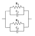
- the semiconductor storage material according to the present invention can be represented by an equivalent circuit in which two electric circuits each consisting of an electric double layer are connected in parallel. This allows the semiconductor storage material according to the present invention to become a transistor that exhibits various functions.
- the positively charged dipole created by the (N-O) group of the acetamide group or amino group contributes to the physical adsorption of negatively charged electrons.
- the electrical resistivity of the two electric double layers in the equivalent circuit is preferably 10 -1 to 10 12 ⁇ m, more preferably 10 3 ⁇ m or more and 10 7 ⁇ m or less. Also, it is preferable that the electrical capacitance of each electric double layer is 10 -8 to 10 -5 F.
- the semiconductor energy storage material of the present invention is preferably in the form of a sheet with a thickness of 100 ⁇ m or less, and more preferably in the form of a thin film with a thickness of 20 ⁇ m or less. In this case, a weight reduction effect can be expected in particular.
- fibers containing chitin or chitosan as the main component refer to fibers that contain more than 50% by mass of chitin or chitosan, whose main components are derived from crabs, shrimp, silkworms, cicadas, beetles, and other insects, or antibacterial agents such as filamentous fungi, and more specifically, the cuticles that cover the body surfaces of many invertebrates, such as the exoskeletons (i.e., skins) of arthropods and crustaceans, and the surfaces of the shells of mollusks, and the cell membranes of fungi such as molds and mushrooms.
- invertebrates such as the exoskeletons (i.e., skins) of arthropods and crustaceans, and the surfaces of the shells of mollusks, and the cell membranes of fungi such as molds and mushrooms.
- the fiber is preferably a crystallized amorphous fiber.
- the fiber may have nanocrystals.
- the fiber may also be an amorphous fiber having atomic vacancies.
- the material of the crystallized amorphous fiber may be any material capable of forming an electric double layer on the inner surface, for example, chitin fiber or chitosan fiber.
- chitin fiber and chitosan fiber it is preferable to use chitin nanofiber and chitosan nanofiber, respectively.
- Chitin nanofiber and chitosan nanofiber can increase the electron adsorption ability due to the negative sixth power quantum size effect, and can increase the work function and further increase the dielectric domain.
- the chitin fiber and chitosan fiber may be of any type, and may be, for example, a mucopolysaccharide polymer derived from arthropods or mollusks (e.g., squid), insects (e.g., silkworms, beetles, cicadas, etc.), or microbial products such as fungi (e.g., molds, mushrooms, etc.).
- insects e.g., silkworms, beetles, cicadas, etc.
- microbial products such as fungi (e.g., molds, mushrooms, etc.).
- fibers derived from animals are preferred, and chitosan fibers derived from crabs, shrimp, and mantis shrimp are particularly preferred.
- Chitin and chitosan fibers may have any average fiber diameter.
- the average fiber length and diameter of chitin and chitosan fibers can be adjusted by oxidation and defibration treatments.
- nanofibers are fine fibers with a fiber diameter of about 3 to 400 nm after general refinement, depending on the degree of defibration.
- the average fiber diameter and average fiber length of nanofibers are obtained by averaging the fiber diameters and fiber lengths obtained from the observation of each fiber using an atomic force microscope (AFM) or transmission electron microscope (TEM).
- AFM atomic force microscope
- TEM transmission electron microscope
- Chitin nanofibers and chitosan nanofibers preferably have an average aspect ratio of 50 or less, and are particularly preferably aggregated in a granular form.
- Granular refers to nanofibers that have been finely pulverized by defibration.
- the method of defibrating chitin and chitosan fibers may be any method, but is preferably a method of applying a strong shear force to a dispersion of chitin and chitosan fibers using a high-speed rotation type, colloid mill type, high-pressure type, roll mill type, ultrasonic type, or other device.
- a wet high-pressure or ultra-high-pressure homogenizer that can apply a pressure of 50 MPa or more to a dispersion of chitin and chitosan fibers and can apply a strong shear force as the defibrating device.
- the pressure during defibration is preferably 100 MPa or more, and more preferably 140 MPa or more.
- the number of treatments (passes) with the defibrating device may be one, but is preferably two or more.
- the solvent may be any solvent capable of dispersing chitin fibers or chitosan fibers, such as water, an organic solvent (e.g., ethanol, acetic acid, lactic acid, succinic acid), or a mixture thereof. Since cellulose fibers are hydrophilic, it is particularly preferable that the solvent is water.
- chitin fibers and chitosan fibers may be pretreated as necessary prior to defibration and dispersion processing using a high-pressure homogenizer. Pretreatment can be carried out using a mixing, stirring, emulsifying, and dispersing device such as a high-speed shear mixer.
- the chitin fibers and chitosan fibers may be in the form of an aqueous dispersion obtained after defibration, or may have been subjected to post-treatment as necessary.
- post-treatment include drying (freeze drying, spray drying, tray drying, drum drying, belt drying, thin spreading on a glass plate or the like and drying, fluidized bed drying, microwave drying, heated fan vacuum drying, etc.), re-dispersion in water (any type of dispersion device may be used), pulverization (pulverization using equipment such as a cutter mill, hammer mill, pin mill, jet mill, or bead mill), and high-speed rotary filtration using a Fermix disperser.
- the fibers are preferably made of chitin nanofibers having a width of 3 to 400 nm, or bundles or granular aggregates of the chitosan nanofibers. In this case, the efficiency of forming an electric double layer can be increased.
- the specific surface area of the fiber is preferably 750 to 900 m 2 /g, and particularly preferably 800 to 900 m 2 /g.
- the semiconductor energy storage material according to the present invention is preferably an n-type bulk semiconductor.
- it can be represented by an equivalent circuit consisting of two parallel circuits having two bands, a small current low resistance band and a large current high resistance band.
- the semiconductor energy storage material according to the present invention is preferably made of a bulk semiconductor having N-type negative resistance.
- the material exhibits N-type negative resistance under a high voltage load of 1 kV/cm or more.
- the material can be used, for example, as a DC/AC conversion element or a metal-insulator switching element, and also has a rectifying effect.
- the electricity storage unit according to the present invention is characterized by having the semiconductor electricity storage material according to the present invention and a pair of metal electrodes provided on both sides of the semiconductor electricity storage material so as to sandwich the semiconductor electricity storage material.
- the power storage device according to the present invention is equivalent to a lumped constant capacitor having two macroscopic capacitors between each metal electrode.
- each metal electrode is made of, for example, Al, Cu, gold, polythiophene, etc., and can be manufactured by a sputtering method, a casting method, or a doctor blade method using a microelectromechanical system (M(N)EMS).
- M(N)EMS microelectromechanical system
- it is preferable that the power storage device according to the present invention can operate at temperatures between -269°C and 300°C.
- the electric storage unit according to the present invention may be a parallel integration of a plurality of the semiconductor electric storage materials arranged between a pair of electrodes made of a conductor.
- an electric storage capacity of 600 mJ/m2 or more and a voltage resistance of 1 MV/m or more can be obtained.
- Each electrode is, for example, a metal or a conductive polymer.
- the stacked electricity storage unit according to the present invention is characterized in that it is made up of a stack of multiple electricity storage units according to the present invention.
- the stacked electricity storage unit according to the present invention can be stacked in parallel, for example, by various M(N)EMS methods.
- the stacked electricity storage unit according to the present invention can be represented as a plurality of parallel equivalent circuits connected in an electrically lumped constant manner, and as an electricity storage unit, it can be represented as a plurality of parallel equivalent circuits connected in an electrically distributed constant manner.
- the semiconductor storage material, storage unit, and laminated storage unit of the present invention can be used as semiconductors, for example, as AC transmitters and control devices for microelectronic circuits, overcurrent protection switches, etc. They can also be used in electronic and electrical boards such as various amplifiers, microwave transmitters, pump sources for parametric amplifiers, police radars, door opening and closing systems, trespass detection systems, shunt regulators, and protection circuits.
- the semiconductor storage material, storage unit and laminated storage unit of the present invention can be used as storage units, for example, AC capacitors in microelectronic circuits and storage units on the backside of solar cell panels. They can also be used in various backup power supply modules, coupling elements, noise filters, high-sensitivity acceleration sensors, high-output transformer cutoff prevention devices, and electronic/electrical boards for emergency power supply devices for automobiles or ships. They are also expected to be used in the future as DC storage materials for sunlight in outer space. Examples of storage units include antistatic sheets, lightning protection paper, electronic device shielding paper, film, positively charged garbage adsorption paper, and paint films.
- the present invention provides a semiconductor storage material, a storage battery, and a stacked storage battery that are made of biomaterials and have both semiconducting properties and storage properties.
- FIG. 1 is a perspective view showing the molecular structures of (a) chitin and (b) chitosan constituting the fibers of a semiconductor electricity storage material according to an embodiment of the present invention.
- FIG. 1 is an electrical circuit diagram showing an equivalent circuit of a semiconductor electricity storage material according to an embodiment of the present invention.
- 1 is a graph showing the results of a frequency analysis of current in the N-type negative resistance region of a semiconductor energy storage material according to an embodiment of the present invention.
- 1 is an atomic force microscope (AFM) image of the surface of a semiconductor electricity storage material according to an embodiment of the present invention.
- AFM atomic force microscope
- 1 is a complex plane graph of impedance and a Nyquist diagram of a semiconductor electricity storage material according to an embodiment of the present invention
- 1 is a graph showing the IV characteristics of a semiconductor electricity storage material according to an embodiment of the present invention.
- 1 is a graph showing a discharge curve of a semiconductor electricity storage material according to an embodiment of the present invention.
- 1 is a graph showing the RV characteristics of a semiconductor electricity storage material according to an embodiment of the present invention.
- 1A to 1C are side views, (d) an oblique view, and (e) a side view showing a manufacturing method of a stacked power storage unit according to an embodiment of the present invention using a MEMS method, and (f) an oblique view and (g) a plan view of an equivalent circuit of the manufactured stacked power storage unit.
- the semiconductor storage material according to an embodiment of the present invention is made of crystallized amorphous fibers whose main component is chitin as shown in FIG. 1(a) or chitosan as shown in FIG. 1(b), and is in the form of a sheet having a surface with countless projections and recesses.
- the semiconductor energy storage material according to the embodiment of the present invention has a high dielectric domain structure in which an electric double layer is formed, and can exhibit both semiconducting properties and energy storage properties at the same time.
- the semiconductor energy storage material according to the embodiment of the present invention is equivalent to an electrical lumped constant circuit in which two electrical circuits made of electric double layers are connected in parallel. This makes it possible for the semiconductor energy storage material according to the embodiment of the present invention to become a transistor that exhibits various functions.
- Sample 1 a semiconductor electricity storage material according to an embodiment of the present invention, was produced as follows.
- the raw material used was the shell of the red snow crab, which has a low calcium content.
- the shell was soaked in 2 mol/L (2N) hydrochloric acid for 5 hours, then washed, dried, and crushed, and decalcified by stirring with hydrochloric acid for 48 hours.
- the shell was then placed in 1 mol/L (1N) sodium hydroxide and heated at 100 °C for 12 hours, and this operation was repeated four times to remove proteins.
- the shell was then dried to obtain crude chitin.
- the crude chitin was then soaked in 0.5% potassium permanganate solution for 1 hour, washed, placed in 1% oxalic acid solution, and stirred at 60 °C for 40 minutes to obtain pure white ⁇ -chitin. It was then defibrated using the roll mill method.
- the ⁇ -chitin after defibration was used to prepare a 2% chitin aqueous solution slurry using the doctor blade method, and the water was then evaporated and dried on a hot plate at 100°C to produce the ⁇ -chitin sheet of sample 1.
- a pair of metal electrodes was placed on both sides of the ⁇ -chitin sheet of sample 1 to sandwich sample 1, and various measurements were performed.
- an AC signal was applied between each electrode using the AC impedance method to measure the absolute value of the impedance of sample 1 and the phase difference between the voltage and current.
- Carbon with a work function of 5.0 and Al with a work function of 4.2 were used for each electrode, forming a Schottky junction circuit.
- the measurement results were plotted on a complex plane, it was confirmed that they were plotted along a shape consisting of two circular arcs, one large and one small.
- sample 1 exhibited semiconductor characteristics that showed N-type negative resistance between -70 V and -60 V. It was also confirmed that sample 1 exhibited a rectification effect in which no current flows in the negative charge region, but the current increases sharply in the positive charge region.
- the discharge curve was obtained when Sample 1 was discharged after being charged at 450 V for 3 seconds.
- the amount of stored electricity was calculated from the area enclosed by the discharge curve, the voltage axis, and the time axis, and was found to be 502.5 mJ/ m2 .
- sample 1 was measured and found to be 1.4 g/ cm3 , which was confirmed to be a low density of 2 g/cm3 or less . It was also confirmed that sample 1 could be operated up to 500 V in a low to medium temperature furnace in the range of -269 °C to 200 °C. The specific surface area of sample 1 was measured by the BET adsorption method and found to be 800 m2 /g.
- Sample 2 a semiconductor electricity storage material according to an embodiment of the present invention, was produced as follows.
- the ⁇ -chitin of sample 1 before defibration was defibrated using a homogenizer method, then placed in a 48% sodium hydroxide solution and reacted at 120°C for 30 minutes to obtain chitosan.
- a 2% chitosan aqueous solution slurry was made from the chitosan, dropped onto a Si substrate of a spin coater, and the Si substrate was rotated at 500 rpm to form a thin film, which was then dried by evaporating the water on a hot plate at 100°C to produce a chitosan sheet.
- the surface of the chitosan sheet of sample 2 was observed with an atomic force microscope (AFM).
- An AFM image of sample 2 is shown in Figure 4.
- Figure 4 it was confirmed that the chitosan sheet of sample 2 was formed from connected bundles or granular aggregates of fibrous chitosan nanofibers of 200 to 400 nm. It was also confirmed that the chitosan nanofibers were amorphous fibers.
- a pair of metal electrodes was placed on both sides of the chitosan sheet of sample 2 to sandwich sample 2, and various measurements were performed.
- the absolute value of the impedance of sample 2 and the phase difference between the voltage and current were measured using the AC impedance method in the same manner as in Example 1.
- the measurement results are plotted on a complex plane in Figure 5. As shown in Figure 5, it was confirmed that the measurement results were plotted along a shape consisting of two circular arcs, one large and one small.
- sample 2 is equivalent to an electrical lumped constant circuit having two macroscopic capacitors (electric double layers) shown in Fig. 2, and forms a semiconductor having two bands, a small current low resistance band and a large current high resistance band.
- Fig. 7 the discharge curve of sample 2 when it was discharged after being charged at 450 V for 3 seconds is shown in Fig. 7.
- the amount of stored electricity was calculated from the area enclosed by the discharge curve, voltage axis, and time axis (Discharge Time) shown in Fig. 7, and was found to be 1004.4 mJ/ m2 . It is considered that the amount of stored electricity is improved with a high voltage load of 400 V or more.
- sample 2 was measured and found to be 1.0 g/ cm3 , a low density of 2 g/cm3 or less . It was also confirmed that sample 2 can be operated up to 500 V in a low to medium temperature furnace in the range of -269 °C to 200 °C. The specific surface area of sample 2 was measured by the BET adsorption method and found to be 800 m2 /g.
- Sample 3 a semiconductor electricity storage material according to an embodiment of the present invention, was produced as follows. Squid bone cores were used as raw materials. The raw materials were soaked in 2 mol/L (2N) hydrochloric acid for 5 hours, washed with water, dried, crushed, and further decalcified with hydrochloric acid while stirring for 48 hours. After that, the raw materials were placed in 1 mol/L (1N) sodium hydroxide and heated at 100 °C for 12 hours, and this operation was repeated four times to remove proteins. The crude chitin was then dried to obtain crude chitin.
- the crude chitin was then soaked in 0.5% potassium permanganate solution for 1 hour, washed with water, placed in 1% oxalic acid solution, and stirred at 60 °C for 40 minutes to obtain ⁇ -chitin.
- This ⁇ -chitin has balanced sugar chains and loose hydrogen bonds, making it easy to handle, but the yield of the raw squid bone cores was less than that of the crab, the raw material of sample 1.
- the ⁇ -chitin was defibrated using the cutter mill method, and then a 2% chitin aqueous solution slurry was made using the doctor blade method. The water was evaporated and the mixture was dried on a hot plate at 50°C to produce the ⁇ -chitin sheet of sample 1.
- a pair of metal electrodes was provided on both sides of the ⁇ -chitin sheet of sample 3 so as to sandwich sample 3, and various measurements were performed.
- the absolute value of the impedance of sample 3 and the phase difference between the voltage and the current were measured by the AC impedance method in the same manner as in Example 1, and a Nyquist diagram was obtained.
- sample 3 is equivalent to an electrical lumped constant circuit having two macroscopic capacitors (electric double layers) as shown in Figure 2, and forms a semiconductor having two bands, a small current low resistance band and a large current high resistance band.
- sample 3 was charged at 450 V for 3 seconds, and then discharged to obtain a discharge curve.
- the amount of stored electricity was calculated from the area enclosed by the discharge curve, the voltage axis, and the time axis, and was found to be 240.1 mJ/ m2 .
- sample 3 was measured and found to be 1.5 g/ cm3 , which was confirmed to be a low density of 2 g/cm3 or less . It was also confirmed that sample 3 could be operated up to 500 V in a low to medium temperature furnace in the range of -269 °C to 200 °C. The specific surface area of sample 3 was measured by the BET adsorption method and found to be 800 m2 /g.
- the sample type, defibration processing method used during manufacturing, structure (crystalline/amorphous), density, electrical resistivity, electrical capacity, and stored electricity amount for the semiconductor energy storage materials samples 1 to 3 are summarized in Table 1.
- each of the semiconductor storage materials of samples 1 to 3 is composed of two electric lumped constant circuits, with AC electric resistance R 1 of 14 to 35 k ⁇ m, R 2 of 5 to 21 k ⁇ m, and electric capacitance C 1 of the electric double layer of 10 -8 F to 10 -6 F, and C 2 of 10 -7 F to 10 -5 F, as shown in Figure 2. It was confirmed that this is the reason for the appearance of a bulk n-type semiconductor phenomenon rather than a pn junction. It was also confirmed that the density was low, at 2 g/cm 3 or less. It was also confirmed that each of samples 1 to 3 has storage properties and can operate up to 500 V in the range of -269 °C to 200 °C. It was also confirmed that the specific surface area of samples 1 to 3 was 800 m 2 /g. From these facts, it is considered that each of the semiconductor storage materials made of biomaterials of samples 1 to 3 will be the most suitable material for the low-current field.
- sample 2 When sample 2 was irradiated with a strong electron beam of 3 mA/ m2 , it was confirmed that it had electrical resistance up to 200 keV. This is more than twice the electrical resistance of carbon nanotubes, which has an electrical resistance of 80 keV.
- FIG. 9 shows a stacked electricity storage unit according to an embodiment of the present invention.
- the stacked electricity storage body according to the embodiment of the present invention is manufactured by the MEMS method using the sheet-shaped semiconductor electricity storage material of sample 2 as follows. First, as shown in FIG. 9(a), a Cu layer (500 nm thick) is formed on the surface of a glass substrate (40 ⁇ 40 ⁇ 0.5 mm) by sputtering. Next, as shown in FIG. 9(b), a sheet-shaped sample 2 is placed on the Cu layer, and further, as shown in FIG. 9(c), an Al layer (500 nm thick) is formed on the sheet-shaped sample 2 by sputtering.
- This structure corresponds to samples 1 to 3 having metal electrodes on both sides thereof, which were used in the various measurements of Examples 1 to 3.
- the glass substrate is removed to form a single basic body, and multiple such basic bodies are stacked to produce a stacked electricity storage unit according to an embodiment of the present invention, as shown in Figure 9(e).
- the stacked electricity storage unit thus produced has multiple semiconductor electricity storage materials joined in parallel, with the Al layer of the topmost basic body and the carbon layer of the bottommost basic body serving as terminals, as shown in Figures 9(f) and (g).
- the semiconductor storage material according to the embodiment of the present invention can be used in a wide range of applications, from low-voltage applications such as mobile phones, drones, and wall-mounted televisions to heavy-voltage applications such as ships and airplanes, taking advantage of its light weight. It can also be used in power supply modules for lightning arresters, welding, and over-discharge prevention, noise filters, door opening and closing systems, trespassing detection systems, pedestrian safety systems, and other sensors, microelectronics control devices, remote vibration detectors, transmitters, and other electronic and electrical substrates. Examples of storage bodies include antistatic sheets, lightning protection paper, electronic device shielding paper, films, positively charged garbage adsorption paper, and paint films.
Landscapes
- Engineering & Computer Science (AREA)
- Power Engineering (AREA)
- Chemical & Material Sciences (AREA)
- Chemical Kinetics & Catalysis (AREA)
- Electrochemistry (AREA)
- Microelectronics & Electronic Packaging (AREA)
- Manufacturing & Machinery (AREA)
- Electric Double-Layer Capacitors Or The Like (AREA)
Priority Applications (2)
| Application Number | Priority Date | Filing Date | Title |
|---|---|---|---|
| JP2025531411A JPWO2025009274A1 (https=) | 2023-07-05 | 2024-05-16 | |
| CN202480043018.1A CN121399712A (zh) | 2023-07-05 | 2024-05-16 | 半导体蓄电材料、蓄电体及层叠蓄电体 |
Applications Claiming Priority (2)
| Application Number | Priority Date | Filing Date | Title |
|---|---|---|---|
| JP2023111062 | 2023-07-05 | ||
| JP2023-111062 | 2023-07-05 |
Publications (1)
| Publication Number | Publication Date |
|---|---|
| WO2025009274A1 true WO2025009274A1 (ja) | 2025-01-09 |
Family
ID=94171837
Family Applications (1)
| Application Number | Title | Priority Date | Filing Date |
|---|---|---|---|
| PCT/JP2024/018185 Ceased WO2025009274A1 (ja) | 2023-07-05 | 2024-05-16 | 半導体蓄電材料、蓄電体および積層蓄電体 |
Country Status (3)
| Country | Link |
|---|---|
| JP (1) | JPWO2025009274A1 (https=) |
| CN (1) | CN121399712A (https=) |
| WO (1) | WO2025009274A1 (https=) |
Citations (3)
| Publication number | Priority date | Publication date | Assignee | Title |
|---|---|---|---|---|
| US20070242415A1 (en) * | 2006-04-14 | 2007-10-18 | Maxwell Technologies, Inc. | Energy Storage Device Having A Separator Blocking Parasitic Ions |
| WO2011037003A1 (ja) | 2009-09-24 | 2011-03-31 | 国立大学法人東北大学 | 電界効果型トランジスタおよび集積回路 |
| WO2021166813A1 (ja) | 2020-02-18 | 2021-08-26 | 国立大学法人東北大学 | 蓄電材料及びウルトラ蓄電体 |
-
2024
- 2024-05-16 WO PCT/JP2024/018185 patent/WO2025009274A1/ja not_active Ceased
- 2024-05-16 JP JP2025531411A patent/JPWO2025009274A1/ja active Pending
- 2024-05-16 CN CN202480043018.1A patent/CN121399712A/zh active Pending
Patent Citations (3)
| Publication number | Priority date | Publication date | Assignee | Title |
|---|---|---|---|---|
| US20070242415A1 (en) * | 2006-04-14 | 2007-10-18 | Maxwell Technologies, Inc. | Energy Storage Device Having A Separator Blocking Parasitic Ions |
| WO2011037003A1 (ja) | 2009-09-24 | 2011-03-31 | 国立大学法人東北大学 | 電界効果型トランジスタおよび集積回路 |
| WO2021166813A1 (ja) | 2020-02-18 | 2021-08-26 | 国立大学法人東北大学 | 蓄電材料及びウルトラ蓄電体 |
Non-Patent Citations (15)
| Title |
|---|
| M. FUKUHARAH. KAWARADA: "Room-temperature amorphous alloy field-effect transistor exhibiting particle and wave electronic transport", J. APPL. PHYS., vol. 117, 2015, pages 084302 |
| M. FUKUHARAH. YOSHIDAK. KOYAMAA. INOUEY. MIURA: "Electronic transport behaviors of Ni-Ngb-Zr-H glassy alloys", J. APPL. PHYS., vol. 107, 2010, pages 033703 |
| M. FUKUHARAH. YOSHIDAM. SATOK. SUGAWARAT. TAKEUCHII. SEKIT. SUEYOSHI: "Superior electric storage in de-alloyed and anodic oxidized Ti-Ni-Si glassy alloy ribbons", PHYS. STAT. SOL. RRL, vol. 7, no. 7, 2013, pages 477 - 480 |
| M. FUKUHARAK. SUGAWARA: "Anodic oxidization of Ti-Ni-Si amorphous alloy ribbons and their capacitive and resistive properties", THIN SOLID FILMS, vol. 595, 2015, pages 1 - 4 |
| M. FUKUHARAK. SUGAWARA: "Electric charging/discharging characteristics of super capacitor, using de-alloying and anodic oxidized Ti-Ni-Si amorphous alloy ribbons", NANOSCALE. RES. LETT., vol. 9, 2014, pages 253 |
| M. FUKUHARAT. KURODAF. HASEGAWA: "Amorphous titanium-oxide supercapacitors", SCI. REP, vol. 6, 2016, pages 35870 |
| M. FUKUHARAT. KURODAF. HASEGAWAT. HASHIDAE. KWONK. KONNO: "Amorphous aluminum-oxide supercapacitors", EUROPHYS. LETT., vol. 123, 2018, pages 58004 |
| M. FUKUHARAT. KURODAF. HASEGAWAT. HASHIDAM. TAKEDAK. KONNNON. FUJIMA: "AlO6 clusters' electric storage effect in amorphous alumina supercapacitors", SCI. REP., vol. 11, 2021, pages 1699 |
| M. FUKUHARAT. KURODAF. HASEGAWAT. HASHIDAM. TAKEDAN. FUJIMAM. MORITAT. NAKATANI: "Amorphous cellulose nanofiber supercapacitors", SCI. REP., vol. 11, 2021, pages 6436 |
| M. FUKUHARAT. KURODAF. HASEGAWAT. SUEYOSHI: "Superior electric storage on an amorphous perfluorinated polymer surface", SCI. REP., vol. 6, 2016, pages 22012 |
| M. FUKUHARAT. KURODAF. HASEGAWAY. SHIRAIT. SUWAT. HASHIDAM. NISHIJIMA: "Amorphous titanium-oxide supercapacitors with high capacitance", EUROPHYS. LETT., vol. 128, 2019, pages 58001 |
| M. FUKUHARAT. YOKOTSUKAT. HASHIDAF. OGAWAT. SAKAMOTOM. TAKEDAS. ARAI: "A novel n-type semiconducting biomaterial", SCIENTIFIC REPORTS, vol. 12, 2022, pages 21899 |
| M. FUKUHARAT. YOKOTSUKAT. HASHIDAK. YAMAGUCHIN. FUJIMA: "Amorphous alumina supercapacitors with voltage-charging performance", EUROPHYS. LETT., vol. 141, 2023, pages 36003 |
| M. FUKUHARAT. YOKOTSUKAT. HASHIDAT. MIWAN. FUJIMAM. MORITAT. NAKATANIF. NONOMURA: "Amorphous cellulose nanofiber supercapacitors with voltage-charging performance", SCI. REP., vol. 12, 2022, pages 5619 |
| MIKIO FUKUHARAHAJIME YOSHIDAHIROSHI KAWARADA: "Effect of hydrogen and cluster morphology on the electronic behavior of Ni-Nb-Zr-H glassy alloys with subnanometer-sized icosahedral Zr5Ni5Nb5 clusters", EURO. PHYS. J., D, vol. 67, 2013, pages 40 |
Also Published As
| Publication number | Publication date |
|---|---|
| JPWO2025009274A1 (https=) | 2025-01-09 |
| CN121399712A (zh) | 2026-01-23 |
Similar Documents
| Publication | Publication Date | Title |
|---|---|---|
| Hsu et al. | An eco-friendly, nanocellulose/RGO/in situ formed polyaniline for flexible and free-standing supercapacitors | |
| Pandiselvi et al. | Chitosan-ZnO/polyaniline ternary nanocomposite for high-performance supercapacitor | |
| Alghamdi et al. | Synthesis of carbon nanotubes/titanium dioxide and study of its effect on the optical, dielectric, and mechanical properties of polyvinyl alcohol/sodium alginate for energy storage devices | |
| Wasalathilake et al. | Understanding the structure-property relationships in hydrothermally reduced graphene oxide hydrogels | |
| Wang et al. | Hybrid of MoS2 and reduced graphene oxide: a lightweight and broadband electromagnetic wave absorber | |
| Wang et al. | Tailoring dielectric properties and energy density of ferroelectric polymer nanocomposites by high-k nanowires | |
| Li et al. | Free-standing and transparent graphene membrane of polyhedron box-shaped basic building units directly grown using a NaCl template for flexible transparent and stretchable solid-state supercapacitors | |
| US10629800B2 (en) | Flexible compact nanogenerators based on mechanoradical-forming porous polymer films | |
| Alam et al. | Effect of MWCNT nanofiller on the dielectric performance of bio-inspired gelatin based nanocomposites | |
| Echols et al. | Conformal layer-by-layer assembly of Ti3C2T z MXene-only thin films for optoelectronics and energy storage | |
| CN115053309B (zh) | 蓄电材料及超级蓄电体 | |
| Magisetty et al. | NiFe2O4/Poly (1, 6-heptadiyne) nanocomposite energy-storage device for electrical and electronic applications | |
| Ahmed et al. | A free-standing, flexible PEDOT: PSS film and its nanocomposites with graphene nanoplatelets as electrodes for quasi-solid-state supercapacitors | |
| US20150255227A1 (en) | Self-healing composite, self-healing supercapacitor and methods of fabrication thereof | |
| Anandhavelu et al. | Chitin and chitosan based hybrid nanocomposites for super capacitor applications | |
| Mao et al. | Three-dimensional reduced graphene oxide/poly (3, 4-ethylenedioxythiophene) composite open network architectures for microsupercapacitors | |
| Zhu et al. | Ultrahigh energy density of polymer nanocomposites containing electrostatically self-assembled graphene oxide and hydrotalcite nanosheets | |
| WO2025009274A1 (ja) | 半導体蓄電材料、蓄電体および積層蓄電体 | |
| Liu et al. | Modulating D33 Coefficients Through In Situ AgF and Ag2O Growth in PVDF Composites for High‐Performance Piezoelectric Nanogenerators | |
| Bhutiya et al. | rGO-ZnO nanowire deposited filamentous seaweed nanofibrous cellulose for paper supercapacitor | |
| Toman et al. | New fabrication (PVA-CMC-PbO) nanocomposites structural and electrical properties | |
| Yik et al. | New approaches for energy storage with hyperbranched polymers | |
| Rozana et al. | Dielectric constant of PVDF/MgO nanocomposites thin films | |
| WO2023203846A1 (ja) | 半導体材料および積層半導体材料 | |
| Yadav et al. | Study of bismuth oxide/polystyrene composites as flexible electrodes for super capacitors |
Legal Events
| Date | Code | Title | Description |
|---|---|---|---|
| 121 | Ep: the epo has been informed by wipo that ep was designated in this application |
Ref document number: 24835796 Country of ref document: EP Kind code of ref document: A1 |
|
| ENP | Entry into the national phase |
Ref document number: 2025531411 Country of ref document: JP Kind code of ref document: A |
|
| WWE | Wipo information: entry into national phase |
Ref document number: 2025531411 Country of ref document: JP |
|
| WWE | Wipo information: entry into national phase |
Ref document number: 2024835796 Country of ref document: EP |
|
| NENP | Non-entry into the national phase |
Ref country code: DE |
|
| ENP | Entry into the national phase |
Ref document number: 2024835796 Country of ref document: EP Effective date: 20260205 |