WO2025009154A1 - スピンインダクタ - Google Patents
スピンインダクタ Download PDFInfo
- Publication number
- WO2025009154A1 WO2025009154A1 PCT/JP2023/025134 JP2023025134W WO2025009154A1 WO 2025009154 A1 WO2025009154 A1 WO 2025009154A1 JP 2023025134 W JP2023025134 W JP 2023025134W WO 2025009154 A1 WO2025009154 A1 WO 2025009154A1
- Authority
- WO
- WIPO (PCT)
- Prior art keywords
- layer
- spin
- inductor
- heat dissipation
- wiring
- Prior art date
- Legal status (The legal status is an assumption and is not a legal conclusion. Google has not performed a legal analysis and makes no representation as to the accuracy of the status listed.)
- Ceased
Links
Images







Classifications
-
- H—ELECTRICITY
- H01—ELECTRIC ELEMENTS
- H01F—MAGNETS; INDUCTANCES; TRANSFORMERS; SELECTION OF MATERIALS FOR THEIR MAGNETIC PROPERTIES
- H01F17/00—Fixed inductances of the signal type
Definitions
- This disclosure relates to a spin inductor.
- Inductors along with resistors and capacitors, are major electronic components and are used in a variety of electronic devices.
- a coil is one example of an inductor. There is a trade-off between the size of a coil and the strength of its inductance, and it is difficult to achieve large inductance with a small coil.
- Patent Document 1 Non-Patent Document 1
- Non-Patent Document 2 disclose new inductors that utilize spin vibrations (hereinafter referred to as spin inductors).
- Spin inductors have attracted attention because the smaller the element size, the stronger the inductance strength, making it possible to achieve both miniaturization and inductance strength.
- This disclosure has been made in consideration of the above circumstances, and aims to provide a spin inductor with high heat dissipation efficiency.
- this disclosure provides the following means.
- a spin inductor includes a wiring layer, a first ferromagnetic layer, and a first heat dissipation layer.
- the first ferromagnetic layer is in contact with a first surface of the wiring layer.
- the first heat dissipation layer and the wiring layer sandwich the first ferromagnetic layer in the stacking direction.
- the spin inductor according to the above aspect may further include a first insulating layer.
- the first insulating layer may be located between the first ferromagnetic layer and the first heat dissipation layer in the stacking direction.
- the first insulating layer may contain at least one oxide or nitride selected from the group consisting of Si, Ta, Al, Mg, Si, and Ti.
- the first heat dissipation layer may cover the entire wiring layer and the first ferromagnetic layer when viewed from the stacking direction.
- the spin inductor according to the above aspect may further include a second heat dissipation layer.
- the first heat dissipation layer and the second heat dissipation layer may sandwich the wiring layer and the first ferromagnetic layer in the stacking direction.
- the spin inductor according to the above aspect may further include a first via wiring and a second via wiring.
- the first via wiring and the second via wiring may each be connected to the wiring layer, and the second heat dissipation layer may be between the first via wiring and the second via wiring.
- the longitudinal direction of the first heat dissipation layer may be a first direction, and the longitudinal direction of the second heat dissipation layer may intersect with the first direction.
- the wiring layer may include a main portion through which a current flows in a first direction and a first branch portion branching off from the main portion. At least a portion of the first branch portion may be configured to extend along the main portion at a position shifted in a second direction intersecting the first direction.
- the wiring layer may further include a second branch portion. At least a portion of the second branch portion may be shifted in a second direction intersecting the first direction and extend along the main portion, and there may be a gap between the first branch portion and the second branch portion.
- the spin inductor according to the above aspect may further include a first connection portion connecting the first heat dissipation layer and the wiring layer.
- the spin inductor according to the above aspect may further include a first connection portion connecting the first heat dissipation layer and the wiring layer, and the first connection portion may be connected to the first branch portion of the wiring layer.
- the spin inductor according to the above aspect may further include a second connection portion connecting the first heat dissipation layer and the second heat dissipation layer.
- the spin inductor according to the above aspect may further include a third connection portion connecting the wiring layer, the first heat dissipation layer, and the second heat dissipation layer.
- the first heat dissipation layer may include any one selected from the group consisting of Ta, NiCr, Ti, SiN, TiN, ferrite, Ni, and Fe.
- the wiring layer may be configured to be able to inject spins into the first ferromagnetic layer, and the magnetization of the first ferromagnetic layer may be configured to precess due to the injected spins.
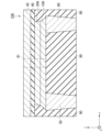
- FIG. 1 is a cross-sectional view of a spin inductor according to a first embodiment.
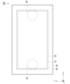
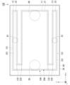
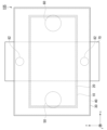
- FIG. 1 is a plan view of a spin inductor according to a first embodiment.
- 3A to 3C are schematic diagrams for explaining the function of the spin inductor according to the first embodiment.
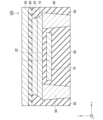
- FIG. 11 is a cross-sectional view of a spin inductor according to a second embodiment.
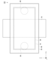
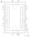
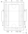
- FIG. 11 is a plan view of a spin inductor according to a second embodiment.
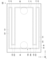
- FIG. 13 is a plan view of a spin inductor according to a third embodiment.
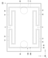
- FIG. 13 is a plan view of a spin inductor according to a fourth embodiment.
- FIG. 13 is a cross-sectional view of a spin inductor according to a fifth embodiment.
- FIG. 13 is a plan view of a spin inductor according to a fifth embodiment.
- FIG. 13 is a plan view of a first modified example of the spin inductor according to the fifth embodiment.
- FIG. 13 is a plan view of a second modified example of the spin inductor according to the fifth embodiment.
- FIG. 13 is a cross-sectional view of a spin inductor according to a sixth embodiment.
- FIG. 13 is a plan view of a spin inductor according to a sixth embodiment.
- FIG. 13 is a cross-sectional view of a spin inductor according to a seventh embodiment.
- FIG. 13 is a plan view of a spin inductor according to a seventh embodiment.
- FIG. 23 is a plan view of a first modified example of the spin inductor according to the seventh embodiment.
- 1 is a diagram illustrating an example of application of the spin inductor according to the present embodiment.
- One direction of the plane in which each layer extends is the x-direction, and the direction perpendicular to the x-direction is the y-direction.
- the first direction connecting the first via wiring 50 and the second via wiring 60 along the wiring layer 10 is the x-direction.
- the second direction perpendicular to the x-direction is, for example, the y-direction.
- the thickness direction of each layer is the z-direction.
- the x-direction and y-directions are perpendicular to the z-direction.
- the z-direction is an example of a stacking direction.
- Fig. 1 is a cross-sectional view of a spin inductor 100 according to the first embodiment.
- Fig. 1 is a view of the spin inductor 100 cut along an xz plane passing through the center of the wiring layer 10 in the y direction.
- Fig. 2 is a plan view of the spin inductor 100 according to the first embodiment. In Fig. 2, components located below the first heat dissipation layer 30 are illustrated by dotted lines.
- the spin inductor 100 comprises a wiring layer 10, a first ferromagnetic layer 20, a first heat dissipation layer 30, a first insulating layer 40, a first via wiring 50, and a second via wiring 60.
- the spin inductor 100 is surrounded by an insulating layer 90.
- the insulating layer 90 is an insulating layer that provides insulation between wirings in a multilayer wiring and between elements.
- the insulating layer 90 can be made of a material similar to that used for insulating layers in semiconductor devices.
- the insulating layer 90 can be made of, for example, silicon oxide (SiO x ), silicon nitride (SiN x ), silicon carbide (SiC), chromium nitride (CrN), silicon carbonitride ( SiCN ), silicon oxynitride (SiON), aluminum oxide (Al 2 O 3 ), or zirconium oxide (ZrO x ).
- the spin inductor 100 is an inductor that operates by vibration of magnetization in a magnetic material.
- the spin inductor 100 cuts the high-frequency components of the current and passes the constant components of the current.
- the current flows along the wiring layer 10 between the first via wiring 50 and the second via wiring 60.
- the spin inductor 100 is disposed in a portion where it is desired to cut off the high-frequency current.
- the high-frequency current is cut by the spin inductor 100, but a direct current flows through the spin inductor 100.
- the spin inductor 100 is a resistor.
- the spin inductor 100 may have multiple inductor layers each consisting of a wiring layer 10 and a first ferromagnetic layer 20.
- a spacer layer is sandwiched between adjacent inductor layers.
- the spacer layer may be a conductor, a semiconductor, or an insulator.
- the wiring layer 10 includes any of a metal, alloy, intermetallic compound, metal boride, metal carbide, metal silicide, and metal phosphide that has the function of generating a spin current by the spin Hall effect when a current flows.
- the wiring layer 10 is sometimes called spin orbit torque wiring.
- the wiring layer 10 may contain a magnetic metal.
- the magnetic metal is a ferromagnetic metal or an antiferromagnetic metal.
- a small amount of magnetic metal contained in a nonmagnetic material becomes a scattering factor for spin.
- a small amount is, for example, 3% or less of the total molar ratio of the elements constituting the wiring layer.
- the wiring layer 10 may include a topological insulator.
- a topological insulator is a material in which the interior is an insulator or a high resistance material, but a spin-polarized metallic state occurs on its surface.
- an internal magnetic field is generated due to spin-orbit interaction.
- a new topological phase appears due to the effect of spin-orbit interaction even in the absence of an external magnetic field.
- a topological insulator can generate pure spin current with high efficiency due to strong spin-orbit interaction and the breaking of inversion symmetry at the edges.
- current flows only on the surface, so a high current density can be achieved with a small amount of current.
- topological insulators examples include Sn, SnTe, Bi1.5Sb0.5Te1.7Se1.3 , TlBiSe2 , Bi2Te3 , Bi1 -xSbx , ( Bi1 -xSbx ) 2Te3 , etc. Topological insulators are capable of generating spin currents with high efficiency.
- the first ferromagnetic layer 20 contacts the first surface of the wiring layer 10.
- the first ferromagnetic layer 20 contacts, for example, the top surface of the wiring layer 10.
- the first ferromagnetic layer 20 is a ferromagnetic material.
- the ferromagnetic material is, for example, a metal selected from the group consisting of Cr, Mn, Co, Fe, and Ni, an alloy containing one or more of these metals, or an alloy containing these metals and at least one of the elements B, C, and N.
- the ferromagnetic material is, for example, Co-Fe, Co-Fe-B, Ni-Fe, Co-Ho alloy, Sm-Fe alloy, Fe-Pt alloy, Co-Pt alloy, CoCrPt alloy.
- the CoCrPt alloy and the L10 type CoFe alloy have large saturation magnetization and strong magnetic anisotropy, and when these are used for the first ferromagnetic layer 20, the resonant frequency of the spin inductor 100 becomes high.
- the first ferromagnetic layer 20 may also be a magnetic insulator.
- the wiring layer 10 is a topological insulator. Since current flows only at the junction between the magnetic insulator and the topological insulator, current loss can be reduced, and energy loss due to heat generation, etc. can be reduced.
- the spin Hall effect is a phenomenon in which, when electric current is passed, a spin current is induced in a direction perpendicular to the direction of electric current flow (for example, the z direction) due to spin-orbit interaction.
- the spin Hall effect is similar to the regular Hall effect in that the direction of movement of moving charges (electrons) can be bent.
- the regular Hall effect the direction of movement of charged particles moving in a magnetic field is bent by the Lorentz force.
- the direction of spin movement can be bent simply by moving electrons (current flow) even in the absence of a magnetic field.
- the spin S1 polarized in the -y direction is bent in the +z direction relative to the direction of travel
- the spin S2 polarized in the +y direction is bent in the -z direction relative to the direction of travel.
- the spins S1 generated in the wiring layer 10 are injected into the first ferromagnetic layer 20.
- the distance between the wiring layer 10 and the first ferromagnetic layer 20 equal to or less than the spin diffusion length of the spins S1
- the spins S1 generated in the wiring layer 10 can be efficiently injected into the first ferromagnetic layer 20.
- Another layer may be inserted between the wiring layer 10 and the first ferromagnetic layer 20.
- the magnetization M20 of the first ferromagnetic layer 20 precesses due to the spins S1 injected from the wiring layer 10.
- the coercive force of the magnetization M20 and the magnitude of the current flowing through the wiring layer 10 are adjusted so that the magnetization M20 precesses without being reversed due to the injected spins S1.
- the magnetization M20 in the initial state in which neither an external magnetic field nor a current is applied to the spin inductor 100, the magnetization M20 preferably has a component oriented in the z direction or the x direction, and is more preferably oriented in the z direction.
- no current flows refers to a state in which no potential difference is applied to the wiring layer 10.
- no external magnetic field is applied refers to a state in which no magnetic field is intentionally applied to the first ferromagnetic layer 20.
- magnetization M20 When magnetization M20 is oriented in the y direction, magnetization reversal may occur even when no external magnetic field is applied, and the precession of magnetization may not be maintained. When magnetization M20 is oriented in the x or z direction, magnetization reversal is unlikely to occur in the absence of a magnetic field. Since the spin inductor 100 exhibits its inductor function by utilizing energy conversion between a magnetic moment and a current, when the precession of magnetization stops, the inductor function is not fully exhibited.
- the spin inductor 100 generates a resonance phenomenon at the ferromagnetic resonance frequency of the first ferromagnetic layer 20, so it is difficult for the spin inductor 100 to operate stably as an inductor near the resonance frequency. Therefore, the spin inductor 100 is used at a frequency sufficiently lower or sufficiently higher than the ferromagnetic resonance frequency of the spin inductor 100. This sufficiently low or sufficiently high frequency generally indicates a frequency that is deviated from the ferromagnetic resonance frequency by 5% or more, based on the ferromagnetic resonance frequency.
- the spin inductor 100 can generate inductance even at frequencies exceeding, for example, 10 GHz or 1 THz. Furthermore, the inductance generated by the spin inductor 100 functions satisfactorily even at 1 nH or less.
- the spin inductor 100 exhibits an inductance of several nH to several hundred nH.
- the spin inductor 100 functions as an inductor as the magnetization M20 of the first ferromagnetic layer 20 precesses due to the spins injected from the wiring layer 10.
- This spin inductor 100 operates on a different principle than a coil and can be made smaller. For example, even if the maximum width of the spin inductor 100 when viewed in a plane from the z direction is 0.003 mm or less, it can achieve an inductance of 0.1 ⁇ H or more and 10 ⁇ H or less. Small inductance elements are particularly in demand in areas where it is difficult to incorporate large elements, such as space and cryogenic temperatures.
- the inductor 100 can efficiently dissipate heat from the first heat dissipation layer 30 even if heat is generated in the thin-film inductor layer.
- Fig. 4 is a cross-sectional view of the spin inductor 101 according to the second embodiment.
- Fig. 5 is a plan view of the spin inductor 101 according to the second embodiment.
- the same components as those in the spin inductor 100 according to the first embodiment are denoted by the same reference numerals and will not be described.
- the spin inductor 101 includes a wiring layer 10, a first ferromagnetic layer 20, a first heat dissipation layer 30, a first insulating layer 40, a first via wiring 50, a second via wiring 60, and a second heat dissipation layer 70.
- the spin inductor 101 is surrounded by an insulating layer 90.
- the spin inductor 101 differs from the spin inductor 100 according to the first embodiment in that it includes a second heat dissipation layer 70.
- the second heat dissipation layer 70 is located below the wiring layer 10.
- the second heat dissipation layer 70 and the first heat dissipation layer 30 sandwich the wiring layer 10 and the first ferromagnetic layer 20 in the z direction.
- the second heat dissipation layer 70 is located between the first via wiring 50 and the second via wiring 60 in the x direction.
- the second heat dissipation layer 70 is surrounded by an insulating layer 90, and the second heat dissipation layer 70 is insulated from the wiring layer 10, the first via wiring 50, and the second via wiring 60.
- the longitudinal direction of the second heat dissipation layer 70 is the y direction.
- the second heat dissipation layer 70 is, for example, a rectangle with the longitudinal direction in the y direction.
- the longitudinal direction of the second heat dissipation layer 70 may be different from the longitudinal direction of the first heat dissipation layer 30.
- the longitudinal direction of the first heat dissipation layer 30 may be the x direction
- the longitudinal direction of the second heat dissipation layer 70 may be the y direction.
- the spin inductor 101 according to the second embodiment has the same effect as the spin inductor 100 according to the first embodiment.
- the heat dissipation efficiency of the spin inductor 101 can be further improved.
- Fig. 6 is a plan view of the spin inductor 102 according to the third embodiment.
- the cross section of the spin inductor 102 according to the third embodiment is equivalent to that of Fig. 1.
- the same components as those in the spin inductor 100 according to the first embodiment are denoted by the same reference numerals, and description thereof will be omitted.
- the spin inductor 102 includes a wiring layer 10A, a first ferromagnetic layer 20A, a first heat dissipation layer 30, a first insulating layer 40, a first via wiring 50, and a second via wiring 60.
- the shapes of the wiring layer 10A and the first ferromagnetic layer 20A of the spin inductor 102 are different from those of the wiring layer 10 and the first ferromagnetic layer 20 of the spin inductor 100 according to the first embodiment.
- the branch portion 12 has a first portion 121 and a second portion 122.
- the first portion 121 is positioned offset in the y direction from the main portion 11 and extends along the main portion 11.
- the first portion 121 may extend in a direction tilted from the x direction.
- the second portion 122 is a portion that connects the main portion 11 and the first portion 121.
- the second portion 122 protrudes from the main portion 11 with a y direction component.
- the branch portion 13 has a first portion 131 and a second portion 132.
- the first portion 131 is positioned offset in the y direction from the main portion 11 and extends along the main portion 11.
- the first portion 131 may extend in a direction tilted from the x direction.
- the second portion 132 is a portion that connects the main portion 11 and the first portion 131.
- the second portion 132 protrudes from the main portion 11 with a y direction component.
- the current flows through the main portion 11, and almost no current flows through the branch portions 12 and 13.
- the current flows in the x direction.
- the current density in the branch portions 12 and 13 is, for example, 1 A/cm2 or less , and preferably 0.1 A/ cm2 or less. Therefore, even when a current is passed through the wiring layer 10A, the branch portions 12 and 13 do not generate much heat.
- the branch portions 12 and 13 dissipate the heat generated in the main portion 11.
- the first ferromagnetic layer 20A also has a main portion 21 and branch portions 22 and 23.
- the main portion 21 is a portion that connects the first via wiring 50 and the second via wiring 60.
- the branch portions 22 and 23 are each a portion that branches off from the main portion 21.
- the branch portion 22 has a first portion 221 and a second portion 222.
- the first portion 221 is positioned offset in the y direction from the main portion 21 and extends along the main portion 21.
- the first portion 221 may extend in a direction tilted from the x direction.
- the second portion 222 is a portion that connects the main portion 21 and the first portion 221.
- the second portion 222 protrudes from the main portion 21 with a y direction component.
- the branch portion 23 has a first portion 231 and a second portion 232.
- the first portion 231 is positioned offset in the y direction from the main portion 21 and extends along the main portion 21.
- the first portion 231 may extend in a direction tilted from the x direction.
- the second portion 232 is a portion that connects the main portion 21 and the first portion 231.
- the second portion 232 protrudes from the main portion 21 with a y direction component.
- the current flows through the main portion 21, and almost no current flows through the branch portions 22 and 23.
- the current flows in the x direction.
- the current density in the branch portions 22 and 23 is, for example, 1 A/ cm2 or less, and preferably 0.1 A/cm2 or less.
- the branch portions 22 and 23 dissipate heat generated in the main portion 21.
- the spin inductor 102 according to the third embodiment has the same effect as the spin inductor 100 according to the first embodiment.
- the branch portions 12, 13, 22, and 23 function as a heat dissipation path for heat generated in the wiring layer 10A. Therefore, the spin inductor 102 according to the third embodiment has excellent heat dissipation properties. Furthermore, since almost no current flows through the branch portions 12, 13, 22, and 23, the spin inductor 102 having the branch portions 12, 13, 22, and 23 does not significantly reduce the current density of the current flowing through the main portions 11 and 21.
- both the wiring layer 10A and the first ferromagnetic layer 20A have a branch portion, but only one of them may have a branch portion. That is, the wiring layer 10A may be replaced with the wiring layer 10, and the first ferromagnetic layer 20A may be replaced with the first ferromagnetic layer 20.
- Fig. 7 is a plan view of a spin inductor 103 according to a fourth embodiment.
- the cross section of the spin inductor 103 according to the fourth embodiment is equivalent to that of Fig. 1.
- the same components as those in the spin inductor 100 according to the first embodiment are denoted by the same reference numerals, and description thereof will be omitted.
- the spin inductor 103 according to the fourth embodiment includes a wiring layer 10B, a first ferromagnetic layer 20B, a first heat dissipation layer 30, a first insulating layer 40, a first via wiring 50, and a second via wiring 60.
- the shapes of the wiring layer 10B and the first ferromagnetic layer 20B of the spin inductor 100 according to the first embodiment are different from those of the wiring layer 10 and the first ferromagnetic layer 20 of the spin inductor 100 according to the first embodiment.
- the wiring layer 10B has a main portion 11 and branch portions 12, 13, 14, and 15.
- the main portion 11 is a portion that connects the first via wiring 50 and the second via wiring 60.
- the branch portions 12, 13, 14, and 15 are each portions that branch off from the main portion 11.
- the branch portions 12, 13, 14, and 15 are each positioned offset in the y direction from the main portion 11, and have a portion that extends along the main portion 11.
- Each of the branch portions 12 and 13 is an example of a first branch portion.
- Each of the branch portions 14 and 15 is an example of a second branch portion.
- Branch portions 12 and 13 branch off from a first end of main portion 11.
- Branch portions 14 and 15 branch off from a second end of main portion 11.
- the current flows in the x direction.
- the current density in the branch portions 12, 13, 14, and 15 is, for example, 1 A/cm2 or less, and 0.1 A/ cm2 or less. Therefore, even when a current is passed through the wiring layer 10B, the branch portions 12, 13, 14, and 15 do not generate much heat.
- the branch portions 12, 13, 14, and 15 dissipate the heat generated in the main portion 11.
- the first ferromagnetic layer 20B has a main portion 21 and branch portions 22, 23, 24, and 25.
- the main portion 21 is a portion that connects the first via wiring 50 and the second via wiring 60.
- the branch portions 22, 23, 24, and 25 are each portions that branch off from the main portion 21.
- the branch portions 22, 23, 24, and 25 are each positioned offset from the main portion 21 in the y direction, and each have a portion that extends along the main portion 21.
- Branch portions 22 and 23 branch off from a first end of main portion 21.
- Branch portions 24 and 25 branch off from a second end of main portion 21.
- There is a gap G between branch portion 22 and branch portion 24, and branch portion 22 and branch portion 24 are not electrically connected.
- branch portion 23 and branch portion 25 are not electrically connected.
- the branch portions 22, 23, 24, and 25 In the first ferromagnetic layer 20B, most of the current flows through the main portion 21, and almost no current flows through the branch portions 22, 23, 24, and 25. In the main portion 21, the current flows in the x direction.
- the current density in the branch portions 22, 23, 24, and 25 is, for example, 1 A/cm 2 or less, and 0.1 A/cm 2 or less. Therefore, even when a current is passed through the first ferromagnetic layer 20B, the branch portions 22, 23, 24, and 25 do not generate much heat.
- the branch portions 22, 23, 24, and 25 dissipate the heat generated in the main portion 21.
- the spin inductor 103 according to the fourth embodiment has the same effect as the spin inductor 100 according to the first embodiment.
- the branch portions 12, 13, 14, 15, 22, 23, 24, and 25 function as a heat dissipation path for heat generated in the wiring layer 10B. Therefore, the spin inductor 103 according to the fourth embodiment has excellent heat dissipation properties.
- both the wiring layer 10B and the first ferromagnetic layer 20B have branch portions, but only one of them may have a branch portion. That is, the wiring layer 10B may be replaced with the wiring layer 10, and the first ferromagnetic layer 20B may be replaced with the first ferromagnetic layer 20. Furthermore, since almost no current flows through the branch portions 12, 13, 14, 15, 22, 23, 24, and 25, the spin inductor 103 having the branch portions 12, 13, 14, 15, 22, 23, 24, and 25 does not significantly reduce the current density of the current flowing through the main portions 11 and 21.
- Fig. 8 is a cross-sectional view of the spin inductor 104 according to the fifth embodiment.
- Fig. 8 is a view of the spin inductor 104 cut along an xz plane passing through the center of the wiring layer 10A in the y direction.
- components on the front side of the paper are indicated by dotted lines.
- Fig. 9 is a plan view of the spin inductor 104 according to the fifth embodiment.
- components located below the first heat dissipation layer 30 are indicated by dotted lines.
- components similar to those in the spin inductor 102 according to the third embodiment are denoted by the same reference numerals and will not be described.
- the connection portion 81 connects the wiring layer 10A and the first heat dissipation layer 30.
- the connection portion 81 is an example of a first connection portion.
- the connection portion 81 connects, for example, the branch portion 12 and the first heat dissipation layer 30.
- the connection portion 81 also connects, for example, the branch portion 13 and the first heat dissipation layer 30. Since almost no current flows through the branch portions 12 and 13, almost no current flows through the connection portion 81 and the first heat dissipation layer 30. Therefore, in the current flowing between the first via wiring 50 and the second via wiring 60, no current path is formed that flows in the order of the branch portion 12 or branch portion 13, the connection portion 81, and the first heat dissipation layer 30.
- connection part 81 dissipates heat from the branch parts 12 and 13 toward the first heat dissipation layer 30. Therefore, the connection part 81 prevents heat generated in the main part 11 from accumulating in the branch parts 12 and 13.
- the spin inductor 104 according to the fifth embodiment has the same effect as the spin inductor 100 according to the first embodiment.
- the branch portions 12, 13, 22, and 23 function as a heat dissipation path for heat generated in the wiring layer 10A.
- the connection portion 81 also dissipates heat toward the first heat dissipation layer 30, thereby preventing heat from accumulating in the branch portions 12, 13, 22, and 23.
- the spin inductor 104 according to the fifth embodiment has excellent heat dissipation properties.
- connection part 81 an example is shown in which the wiring layer 10A and the first heat dissipation layer 30 are connected by a connection part 81, but the spin inductor according to the fifth embodiment is not limited to this example.
- the spin inductor 104A has a connection portion 81 that connects the wiring layer 10 and the first heat dissipation layer 30.
- the connection portion 81 is preferably located at a position offset in the y direction from the straight line connecting the first via wiring 50 and the second via wiring 60.
- the spin inductor 104 of the first modified example can also efficiently transfer heat generated in the wiring layer 10 to the first heat dissipation layer 30.
- the spin inductor 104A has high heat dissipation properties, although current loss occurs through the connection portion 81.
- the spin inductor 104B has a connection part 81 that connects the wiring layer 10B and the first heat dissipation layer 30.
- the connection part 81 connects, for example, the branch part 12 or the branch part 13 and the first heat dissipation layer 30.
- the other connection part is connected to the branch part 13.
- a current path is formed from the first via wiring 50, the branch part 12, the first heat dissipation layer 30, the connection part 81, the branch part 15, and the second via wiring 60, resulting in current loss.
- the first heat dissipation layer 30 may also be divided into multiple regions, and each region may be electrically insulated. In this case, the current that reaches a portion of the first heat dissipation layer 30 from the connection portion 81 cannot reach other regions, making it difficult for a current path that causes current loss to form.
- Fig. 12 is a cross-sectional view of the spin inductor 105 according to the sixth embodiment.
- Fig. 12 is a view of the spin inductor 105 cut along the xz plane passing through the center of the wiring layer 10 in the y direction.
- components on the front side of the paper are indicated by dotted lines.
- Fig. 13 is a plan view of the spin inductor 104 according to the fifth embodiment.
- components located below the first heat dissipation layer 30 are indicated by dotted lines.
- components similar to those of the spin inductor 101 according to the second embodiment are denoted by the same reference numerals and will not be described.
- the spin inductor 105 includes a wiring layer 10, a first ferromagnetic layer 20, a first heat dissipation layer 30, a first insulating layer 40, a first via wiring 50, a second via wiring 60, a second heat dissipation layer 70, and a connection portion 82.
- the spin inductor 105 differs from the spin inductor 101 according to the second embodiment in that it includes the connection portion 82.
- connection portion 82 connects the first heat dissipation layer 30 and the second heat dissipation layer 70.
- the connection portion 82 is an example of a second connection portion.
- the connection portion 82 conducts heat between the first heat dissipation layer 30 and the second heat dissipation layer 70.
- FIG. 14 is a cross-sectional view of the spin inductor 106 according to the seventh embodiment.
- FIG. 14 is a view of the spin inductor 106 cut along an xz plane passing through the center of the wiring layer 10A in the y direction.
- components on the front side of the paper are indicated by dotted lines.
- FIG. 15 is a plan view of the spin inductor 106 according to the seventh embodiment.
- components located below the first heat dissipation layer 30 are indicated by dotted lines.
- components similar to those in the spin inductor 101 according to the second embodiment and the spin inductor 102 according to the third embodiment are denoted by the same reference numerals and will not be described.
- the spin inductor 106 includes a wiring layer 10A, a first ferromagnetic layer 20A, a first heat dissipation layer 30, a first insulating layer 40, a first via wiring 50, a second via wiring 60, a second heat dissipation layer 70, and a connection portion 83.
- the spin inductor 106 differs from the spin inductor 102 according to the third embodiment in that it includes a second heat dissipation layer 70 and a connection portion 83.
- connection portion 83 connects the wiring layer 10A to the first heat dissipation layer 30 and the second heat dissipation layer 70.
- the connection portion 83 is an example of a third connection portion.
- the connection portion 83 connects, for example, each of the branch portions 12 and 13 to the first heat dissipation layer 30 and the second heat dissipation layer 70. Since almost no current flows through the branch portions 12 and 13, almost no current flows through the connection portion 81, the first heat dissipation layer 30, and the second heat dissipation layer 70. Therefore, the current flowing between the first via wiring 50 and the second via wiring 60 almost never reaches the first heat dissipation layer 30 and the second heat dissipation layer 70 via the connection portion 83.
- connection portion 83 dissipates heat from the branch portions 12 and 13 toward the first heat dissipation layer 30 and the second heat dissipation layer 70. Therefore, the connection portion 83 prevents heat generated in the main portion 11 from accumulating in the branch portions 12 and 13.
- the spin inductor 106 according to the seventh embodiment has the same effect as the spin inductor 100 according to the first embodiment.
- the branch portions 12, 13, 22, and 23 function as a heat dissipation path for heat generated in the wiring layer 10A.
- the connection portion 83 also dissipates heat toward the first heat dissipation layer 30 and the second heat dissipation layer 70, thereby preventing heat from accumulating in the branch portions 12, 13, 22, and 23.
- the spin inductor 106 according to the seventh embodiment has excellent heat dissipation properties.
- the spin inductor according to the seventh embodiment is not limited to this example.
- FIG. 16 is a plan view of a first modified example of the spin inductor according to the seventh embodiment.
- the spin inductor 106B according to the first modified example differs from the spin inductor 106 shown in FIG. 15 in that the wiring layer 10A is wiring layer 10B and the first ferromagnetic layer 20A is first ferromagnetic layer 20B.
- the configurations of the wiring layer 10B and the first ferromagnetic layer 20B are the same as those in FIG. 7.
- the spin inductor 106A has a connection portion 83 that connects the wiring layer 10B, the first heat dissipation layer 30, and the second heat dissipation layer 70.
- the connection portion 83 connects, for example, the branch portion 12 or the branch portion 13, the first heat dissipation layer 30, and the second heat dissipation layer 70.
- the other connection portion 83 is connected to the branch portion 13.
- the first heat dissipation layer 30 may also be divided into multiple regions, and each region may be electrically insulated. In this case, the current that reaches a portion of the first heat dissipation layer 30 from the connection portion 81 cannot reach other regions, making it difficult for a current path that causes current loss to form.
- the first to seventh embodiments have been illustrated above, and the specific configuration of the spin inductor has been described.
- the spin inductor according to the present disclosure is not limited to these exemplary configurations, and various modifications are possible within the scope of the purpose.
- the spin inductor according to the present disclosure can be incorporated into a module, for example, for use.
- Figure 17 shows an example of the use of the spin inductor according to this embodiment.
Landscapes
- Engineering & Computer Science (AREA)
- Power Engineering (AREA)
- Microelectronics & Electronic Packaging (AREA)
- Coils Or Transformers For Communication (AREA)
Abstract
このスピンインダクタは、配線層と、第1強磁性層と、第1放熱層と、を備える。前記第1強磁性層は、前記配線層の第1面に接する。前記第1放熱層と前記配線層は、積層方向において、前記第1強磁性層を挟む。
Description
本開示は、スピンインダクタに関する。
インダクタは、抵抗やキャパシタと並んで主要な電子部品であり、様々な電子機器に用いられている。コイルは、インダクタの一例である。コイルの大きさとインダクタンスの強度とはトレードオフの関係にあり、小型のコイルで大きなインダクタンスを実現することは難しい。
近年、コイルを用いない新たな形態のインダクタに注目が集まっている。コイルを用いない新たな形態のインダクタは、創発インダクタと称される場合がある。例えば、特許文献1、非特許文献1及び非特許文献2には、スピンの振動を利用した新たなインダクタ(以下、スピンインダクタと称する。)が開示されている。スピンインダクタは、素子サイズが小さいほどインダクタンス強度が強くなり、小型化とインダクタンス強度の両立が可能であるとして注目されている。
Yuta Yamane, Shunsuke Fukami, and Junichi Ieda, Physical Review Letters 128,147201 (202).
Yasufumi Arai and Jun'ichi Ieda, Journal of the Physical Society of Japan 92, 074705 (2023).
小型で大きなインダクタンスを示すインダクタが求められている。スピンインダクタを含む創発インダクタは、まだ研究の途中であり、様々な問題を抱えている。その一つがスピンインダクタの放熱性である。スピンインダクタは、薄膜を積層した構造を有し、その薄膜を流れる電流により生じる熱を無視できない。
本開示は上記事情に鑑みてなされたものであり、放熱効率の高いスピンインダクタを提供することを目的とする。
本開示は、上記課題を解決するため、以下の手段を提供する。
(1)第1の態様に係るスピンインダクタは、配線層と、第1強磁性層と、第1放熱層と、を備える。前記第1強磁性層は、前記配線層の第1面に接する。前記第1放熱層と前記配線層は、積層方向において、前記第1強磁性層を挟む。
(2)上記態様に係るスピンインダクタは、第1絶縁層をさらに備えてもよい。前記第1絶縁層は、積層方向において、前記第1強磁性層と前記第1放熱層との間にあってもよい。
(3)上記態様に係るスピンインダクタにおいて、前記第1絶縁層は、Si、Ta、Al、Mg、Si及びTiからなる群から選択された少なくとも一つの酸化物又は窒化物を含んでもよい。
(4)上記態様に係るスピンインダクタにおいて、前記積層方向から見て、前記第1放熱層は、前記配線層及び前記第1強磁性層の全てを覆ってもよい。
(5)上記態様に係るスピンインダクタは、第2放熱層をさらに備えてもよい。前記第1放熱層と前記第2放熱層は、前記積層方向において、前記配線層及び前記第1強磁性層を挟んでもよい。
(6)上記態様に係るスピンインダクタは、第1ビア配線と第2ビア配線とをさらに備えてもよい。前記第1ビア配線及び前記第2ビア配線はそれぞれ、前記配線層に接続され、前記第2放熱層は、前記第1ビア配線と前記第2ビア配線との間にあってもよい。
(7)上記態様に係るスピンインダクタにおいて、前記第1放熱層の長手方向は、第1方向であり、前記第2放熱層の長手方向は、前記第1方向と交差していてもよい。
(8)上記態様に係るスピンインダクタにおいて、前記配線層は、第1方向に電流が流れる主要部と、前記主要部から分岐する第1分岐部とを備えてもよい。前記第1分岐部の少なくとも一部は、前記第1方向と交差する第2方向にずれた位置で、前記主要部に沿う構成でもよい。
(9)上記態様に係るスピンインダクタにおいて、前記配線層は、第2分岐部をさらに備えてもよい。前記第2分岐部の少なくとも一部は、前記第1方向と交差する第2方向にずれた位置で、前記主要部に沿い、前記第1分岐部と前記第2分岐部との間には、ギャップがあってもよい。
(10)上記態様に係るスピンインダクタは、前記第1放熱層と前記配線層とを繋ぐ第1接続部をさらに備えてもよい。
(11)上記態様に係るスピンインダクタは、前記第1放熱層と前記配線層とを繋ぐ第1接続部をさらに備え、前記第1接続部は、前記配線層の前記第1分岐部に接続されていてもよい。
(12)上記態様に係るスピンインダクタは、前記第1放熱層と前記第2放熱層とを繋ぐ第2接続部をさらに備えてもよい。
(13)上記態様に係るスピンインダクタは、前記配線層と前記第1放熱層と前記第2放熱層とを繋ぐ第3接続部をさらに備えてもよい。
(14)上記態様に係るスピンインダクタにおいて、前記第1放熱層は、Ta、NiCr、Ti、SiN、TiN、フェライト、Ni及びFeからなる群から選択されるいずれか一つを含んでもよい。
(15)上記態様に係るスピンインダクタにおいて、前記配線層は、前記第1強磁性層にスピンを注入できるように構成され、前記第1強磁性層の磁化は、注入されたスピンによって歳差運動するように構成されていてもよい。
以下、本実施形態について、図を適宜参照しながら詳細に説明する。以下の説明で用いる図面は、特徴をわかりやすくするために便宜上特徴となる部分を拡大して示している場合があり、各構成要素の寸法比率などは実際とは異なっていることがある。以下の説明において例示される材料、寸法等は一例であって、本開示はそれらに限定されるものではなく、本開示の効果を奏する範囲で適宜変更して実施することが可能である。
まず方向について定義する。各層が広がる面の一方向をx方向、x方向に対して直交する方向をy方向とする。例えば、配線層10に沿って第1ビア配線50と第2ビア配線60とを繋ぐ第1方向をx方向とする。xy面内において、x方向と直交する第2方向を例えばy方向とする。また各層の厚み方向をz方向とする。x方向及びy方向は、z方向に対して直交する。z方向は、積層方向の一例である。
「第1実施形態」
図1は、第1実施形態に係るスピンインダクタ100の断面図である。図1は、配線層10のy方向の中心を通るxz面に沿ってスピンインダクタ100を切断した図である。図2は、第1実施形態に係るスピンインダクタ100の平面図である。図2では、第1放熱層30の下方に位置する構成要素を点線で図示する。
図1は、第1実施形態に係るスピンインダクタ100の断面図である。図1は、配線層10のy方向の中心を通るxz面に沿ってスピンインダクタ100を切断した図である。図2は、第1実施形態に係るスピンインダクタ100の平面図である。図2では、第1放熱層30の下方に位置する構成要素を点線で図示する。
スピンインダクタ100は、配線層10と第1強磁性層20と第1放熱層30と第1絶縁層40と第1ビア配線50と第2ビア配線60とを備える。
スピンインダクタ100の周囲は、絶縁層90で被覆されている。絶縁層90は、多層配線の配線間や素子間を絶縁する絶縁層である。絶縁層90は、半導体デバイスの絶縁層に適用されているものと同様の材料を用いることができる。絶縁層90は、例えば、酸化シリコン(SiOx)、窒化シリコン(SiNx)、炭化シリコン(SiC)、窒化クロム(CrN)、炭窒化シリコン(SiCN)、酸窒化シリコン(SiON)、酸化アルミニウム(Al2O3)、酸化ジルコニウム(ZrOx)である。
スピンインダクタ100は、磁性体中の磁化の振動によって動作するインダクタである。スピンインダクタ100は、電流の高周波成分をカットし、電流の不変成分を通す。電流は、配線層10に沿って、第1ビア配線50と第2ビア配線60との間に流れる。スピンインダクタ100は、高周波電流をカットしたい部分に配設される。高周波電流はスピンインダクタ100でカットされるが、直流電流はスピンインダクタ100を流れる。直流電流にとってスピンインダクタ100は、抵抗である。
スピンインダクタ100は、配線層10と第1強磁性層20とからなるインダクタ層を複数有してもよい。隣接するインダクタ層の間には、例えば、スペーサ層が挟まれる。スペーサ層は、導体でも、半導体でも、絶縁体でもよい。
配線層10は、電流が流れる際のスピンホール効果によってスピン流を発生させる機能を有する金属、合金、金属間化合物、金属硼化物、金属炭化物、金属珪化物、金属燐化物のいずれかを含む。配線層10は、スピン軌道トルク配線と呼ばれる場合もある。
配線層10は、例えば、主成分として非磁性の重金属を含む。重金属は、イットリウム(Y)以上の比重を有する金属を意味する。非磁性の重金属は、例えば、最外殻にd電子又はf電子を有する原子番号39以上の原子番号が大きい非磁性金属である。配線層10は、例えば、Hf、Ta、Wからなる。非磁性の重金属は、その他の金属よりスピン軌道相互作用が強く生じる。スピンホール効果はスピン軌道相互作用により生じる。スピンホール効果によって配線層10内でスピンが偏在しやすくなると、スピン流JSが発生しやすくなる。
配線層10は、磁性金属を含んでもよい。磁性金属は、強磁性金属又は反強磁性金属である。非磁性体に含まれる微量な磁性金属は、スピンの散乱因子となる。微量とは、例えば、配線層を構成する元素の総モル比の3%以下である。スピンが磁性金属により散乱するとスピン軌道相互作用が増強され、電流に対するスピン流の生成効率が高くなる。
配線層10は、トポロジカル絶縁体を含んでもよい。トポロジカル絶縁体は、物質内部が絶縁体又は高抵抗体であるが、その表面にスピン偏極した金属状態が生じている物質である。トポロジカル絶縁体は、スピン軌道相互作用により内部磁場が生じる。トポロジカル絶縁体は、外部磁場が無くてもスピン軌道相互作用の効果で新たなトポロジカル相が発現する。トポロジカル絶縁体は、強いスピン軌道相互作用とエッジにおける反転対称性の破れにより純スピン流を高効率に生成できる。またトポロジカル絶縁体は、表面にのみ電流が流れるため、少ない電流量で高い電流密度を実現できる。
トポロジカル絶縁体は、例えば、Sn、SnTe、Bi1.5Sb0.5Te1.7Se1.3、TlBiSe2、Bi2Te3、Bi1-xSbx、(Bi1-xSbx)2Te3などである。トポロジカル絶縁体は、高効率にスピン流を生成することが可能である。
第1強磁性層20は、配線層10の第1面と接する。第1強磁性層20は、例えば、配線層10の上面と接する。
第1強磁性層20は、強磁性体である。強磁性体は、例えば、Cr、Mn、Co、Fe及びNiからなる群から選択される金属、これらの金属を1種以上含む合金、これらの金属とB、C、及びNの少なくとも1種以上の元素とが含まれる合金等である。
強磁性体は、例えば、Co-Fe、Co-Fe-B、Ni-Fe、Co-Ho合金、Sm-Fe合金、Fe-Pt合金、Co-Pt合金、CoCrPt合金である。CoCrPt合金、L10型のCoFe合金は、飽和磁化が大きく、かつ、磁気異方性も強く、これらを第1強磁性層20に用いると、スピンインダクタ100の共鳴周波数が高くなる。
また第1強磁性層20は、磁性絶縁体でもよい。第1強磁性層20が磁性絶縁体の場合、配線層10はトポロジカル絶縁体であることが特に好ましい。磁性絶縁体とトポロジカル絶縁体の接合面のみに電流が流れるため、電流損失を抑え、発熱等によるエネルギー損失を抑えることができる。
また第1強磁性層20は、フェリ磁性絶縁体や反強磁性絶縁体でもよい。第1強磁性層20が反強磁性絶縁体の場合、配線層10はトポロジカル絶縁体であることが特に好ましい。反強磁性絶縁体とトポロジカル絶縁体の接合面のみに電流が流れるため、電流損失を抑え、発熱等によるエネルギー損失を抑えることができる。さらに、第1強磁性層20が反強磁性絶縁体である場合、第1強磁性層20の共鳴周波数が高くなり、10GHz以上の高周波の領域でも、スピンインダクタは共鳴を起こさない。そのため、第1強磁性層20が反強磁性絶縁体であるスピンインダクタは、広い帯域において、安定的にインダクタンスを示す。例えば、反強磁性絶縁体は、NiO、MnO、Cr2O3、フェライトやガーネットなどの磁性元素を含んだ酸化物、MnSなどの磁性元素を含んだ硫化物、FeCl2などの磁性元素を含んだ塩化物などである。
第1放熱層30は、インダクタ層で生じた熱の放熱を補助する層である。第1放熱層30と配線層10とは、z方向において、第1強磁性層20を挟む。第1放熱層30は、例えば、第1絶縁層40を挟んで、第1強磁性層20に近接する。
第1放熱層30は、例えば、Ta、NiCr、Ti、SiN、TiN、フェライト、Ni及びFeからなる群から選択されるいずれか一つを含む。
第1放熱層30は、例えば、z方向から見て、配線層10及び第1強磁性層20を覆う。第1放熱層30が配線層10及び第1強磁性層20を覆うことで、配線層10及び第1強磁性層20で生じた熱の排熱効率が高まる。
第1絶縁層40は、第1強磁性層20と第1放熱層30との間にある。第1絶縁層40は、例えば、Si、Ta、Al、Mg及びTiからなる群から選択された少なくとも一つの酸化物又は窒化物を含む。第1絶縁層40は、熱伝導率が高いものが好ましく、例えば、MgO、AlN、SiN、TiNである。
第1放熱層30が絶縁体の場合は、第1絶縁層40は無くてもよい。第1放熱層30が導電体の場合は、第1絶縁層40を設けることが好ましい。第1絶縁層40が第1放熱層30と第1強磁性層20との間にあると、配線層10を流れる電流の一部が第1放熱層30に分流することを防ぎ、配線層10を流れる電流の電流密度が低下することを抑制できる。
第1ビア配線50及び第2ビア配線60は、導電性を有する材料を含む。第1ビア配線50及び第2ビア配線60は、例えば、Cu、Al、Ag、Au等である。第1ビア配線50は、配線層10と接する。第2ビア配線60は、第1ビア配線50と異なる位置で、配線層10と接する。第1ビア配線50は、例えば、配線層10の第1端に接続され、第2ビア配線60は、配線層10の第2端に接続される。第1ビア配線50及び第2ビア配線60は、z方向に延びる。
スピンインダクタ100は、第1ビア配線50及び第2ビア配線60に代えて、インダクタ層の側面に接する第1端子と第2端子とを有してもよい。また第1ビア配線50及び第2ビア配線60のそれぞれは、インダクタ層の上面と接してもよい。
本実施形態に係るスピンインダクタ100は、各層を積層する積層工程と、各層を所定の形状に加工する加工工程とを繰り返すことで作製できる。積層工程は、例えば、スパッタリング法、化学気相成長法(CVD法)、電子ビーム蒸着法(EB蒸着法)、原子レーザデポジッション法等を用いることができる。加工工程は、例えば、フォトリソグラフィー法等を用いて行うことができる。
次いで、スピンインダクタ100の機能について説明する。図3は、スピンインダクタ100の機能を説明するための模式図である。
スピンインダクタ100は、配線層10に沿って電流が流れた際にインダクタとして機能する。第1ビア配線50と第2ビア配線60との間に電流を印加すると、配線層10の面内に電流が流れる。
配線層10内を流れる電流は、スピンホール効果によってスピン流を発生させる。
スピンホール効果は、電流を流した場合にスピン軌道相互作用に基づき、電流の流れる方向と直交する方向(例えば、z方向)にスピン流が誘起される現象である。スピンホール効果は、運動(移動)する電荷(電子)が運動(移動)方向を曲げられる点で、通常のホール効果と共通する。通常のホール効果は、磁場中で運動する荷電粒子の運動方向がローレンツ力によって曲げられる。これに対し、スピンホール効果は磁場が存在しなくても、電子が移動するだけ(電流が流れるだけ)でスピンの移動方向が曲げられる。
例えば、配線層10のx方向に電流が流れると、例えば、-y方向に偏極したスピンS1は進行方向に対して+z方向に曲げられ、+y方向に偏極したスピンS2は進行方向に対して-z方向に曲げられる。
配線層10で生じたスピンS1は、第1強磁性層20に注入される。配線層10と第1強磁性層20との距離がスピンS1のスピン拡散長以下であることで、配線層10で生じたスピンS1を第1強磁性層20に効率的に注入できる。配線層10と第1強磁性層20との間には、他の層が挿入されていてもよい。
第1強磁性層20の磁化M20は、配線層10から注入されるスピンS1によって歳差運動する。磁化M20の保磁力と配線層10に流す電流の大きさは調整されており、注入されるスピンS1によって磁化M20が反転せずに歳差運動するように構成されている。
第1強磁性層20の磁化M20が歳差運動すると、磁気モーメントと電流との間でエネルギー変換が生じ、スピンインダクタ100はインダクタ機能を発現する。
磁化M20の歳差運動を保つという観点で、磁化M20は、スピンインダクタ100に外部磁場も電流も印加されていない初期状態で、z方向又はx方向に配向する成分を有することが好ましく、z方向に配向していることがより好ましい。ここで、「電流が流れていない」とは、配線層10に電位差を印加していない状態を意味する。また「外部磁場が印加されていない」とは、第1強磁性層20に意図的な磁場を印加していない状態を意味する。
磁化M20がy方向に配向している場合、外部磁場が印加されていない状態でも、磁化反転が生じ、磁化の歳差運動が維持されない場合がある。磁化M20がx方向又はz方向に配向している場合は、無磁場下では磁化反転が生じにくい。スピンインダクタ100は、磁気モーメントと電流との間のエネルギー変換を利用してインダクタ機能を発現するため、磁化の歳差運動が止まると、インダクタ機能が十分発現されない。
なお、磁化M20がy方向に配向する場合でも、配線層10を流れる電流密度を調整することで磁化の歳差運動を維持することは可能である。
スピンインダクタ100は、第1強磁性層20の強磁性共鳴の周波数で共鳴現象を生じるため、共鳴周波数近傍ではインダクタとしての安定的な動作が困難である。したがって、スピンインダクタ100は、スピンインダクタ100の強磁性共鳴周波数よりも十分低い周波数、または、十分高い周波数で使用される。この十分低い周波数、又は、十分高い周波数は、概ね、強磁性共鳴周波数を基準に、強磁性共鳴周波数から5%以上ずれた周波数を示す。スピンインダクタ100は、例えば、10GHzや1THzを超える周波数でもインダクタンスを発生させることが可能である。またスピンインダクタ100で生じるインダクタンスは、1nH以下でも十分に機能する。
スピンインダクタ100は、電流と磁気モーメントとの間のエネルギー変換を利用してインダクタ機能を発現するため、小型でも強いインダクタンスを発現できる。例えば、z方向から平面視した際のスピンインダクタ100の最大幅が0.003mm以下でも、0.1μH以上10μH以下のインダクタンスを発現できる。小型のインダクタンス素子は、宇宙、極低温等の大型の素子を組み込むことが困難な領域で、特に求められている。また、z方向から平面視した際のスピンインダクタ100の最大幅が数十nmで、長さが数百nmサイズでも、スピンインダクタ100は、数nH~数百nHのインダクタンスを示す。
上述のように、本実施形態に係るスピンインダクタ100は、配線層10から注入されるスピンによって第1強磁性層20の磁化M20が歳差運動することで、インダクタとして機能する。このスピンインダクタ100は、コイルとは異なる原理で動作し、小型化が可能である。例えば、z方向から平面視した際のスピンインダクタ100の最大幅が0.003mm以下でも、0.1μH以上10μH以下のインダクタンスを発現できる。小型のインダクタンス素子は、宇宙、極低温等の大型の素子を組み込むことが困難な領域で、特に求められている。
また本実施形態に係るインダクタ100は、薄膜のインダクタ層で熱が生じた場合でも、第1放熱層30から熱を効率的に逃がすことができる。
「第2実施形態」
図4は、第2実施形態に係るスピンインダクタ101の断面図である。図5は、第2実施形態に係るスピンインダクタ101の平面図である。第2実施形態に係るスピンインダクタ101において、第1実施形態に係るスピンインダクタ100と同様の構成については、同様の符号を付し、説明を省く。
図4は、第2実施形態に係るスピンインダクタ101の断面図である。図5は、第2実施形態に係るスピンインダクタ101の平面図である。第2実施形態に係るスピンインダクタ101において、第1実施形態に係るスピンインダクタ100と同様の構成については、同様の符号を付し、説明を省く。
第2実施形態に係るスピンインダクタ101は、配線層10と第1強磁性層20と第1放熱層30と第1絶縁層40と第1ビア配線50と第2ビア配線60と第2放熱層70とを備える。スピンインダクタ101の周囲は絶縁層90で覆われている。スピンインダクタ101は、第2放熱層70を有する点で、第1実施形態に係るスピンインダクタ100と異なる。
第2放熱層70は、配線層10の下方に位置する。第2放熱層70と第1放熱層30は、z方向に配線層10及び第1強磁性層20を挟む。第2放熱層70は、x方向において、第1ビア配線50と第2ビア配線60との間にある。
第2放熱層70の周囲は、絶縁層90で被覆され、第2放熱層70は、配線層10、第1ビア配線50及び第2ビア配線60と絶縁されている。
z方向から見て、第2放熱層70の長手方向はy方向である。第2放熱層70は、例えば、y方向が長手方向である長方形である。第2放熱層70の長手方向は、第1放熱層30の長手方向と異なっていてもよい。例えば、図5に示すように、第1放熱層30の長手方向がx方向で、第2放熱層70の長手方向がy方向でもよい。第2放熱層70をy方向が長手方向の長方形とすることで、第1ビア配線50と第2ビア配線60との間の限られた空間に、大きな面積の第2放熱層70を配置できる。
第2実施形態に係るスピンインダクタ101は、第1実施形態に係るスピンインダクタ100と同様の効果を奏する。また発熱しやすいインダクタ層を第1放熱層30と第2放熱層70とで挟むことで、スピンインダクタ101の排熱効率をより高めることができる。
「第3実施形態」
図6は、第3実施形態に係るスピンインダクタ102の平面図である。第3実施形態に係るスピンインダクタ102の断面は、図1と同等である。第3実施形態に係るスピンインダクタ102において、第1実施形態に係るスピンインダクタ100と同様の構成については、同様の符号を付し、説明を省く。
図6は、第3実施形態に係るスピンインダクタ102の平面図である。第3実施形態に係るスピンインダクタ102の断面は、図1と同等である。第3実施形態に係るスピンインダクタ102において、第1実施形態に係るスピンインダクタ100と同様の構成については、同様の符号を付し、説明を省く。
第3実施形態に係るスピンインダクタ102は、配線層10Aと第1強磁性層20Aと第1放熱層30と第1絶縁層40と第1ビア配線50と第2ビア配線60とを備える。スピンインダクタ102は、配線層10A及び第1強磁性層20Aの形状が、第1実施形態に係るスピンインダクタ100の配線層10及び第1強磁性層20と異なる。
配線層10Aは、主要部11と分岐部12、13とを有する。主要部11は、第1ビア配線50と第2ビア配線60とを繋ぐ部分である。分岐部12、13はそれぞれ、主要部11から分岐した部分である。分岐部12、13のそれぞれは、第1分岐部の一例である。
分岐部12は、第1部分121と第2部分122とを有する。第1部分121は、主要部11からy方向にずれた位置にあり、主要部11に沿って延びる。第1部分121は、x方向から傾いた方向に延びていてもよい。第2部分122は、主要部11と第1部分121とを繋ぐ部分である。第2部分122は、主要部11からy方向の成分をもって突出している。
同様に、分岐部13は、第1部分131と第2部分132とを有する。第1部分131は、主要部11からy方向にずれた位置にあり、主要部11に沿って延びる。第1部分131は、x方向から傾いた方向に延びていてもよい。第2部分132は、主要部11と第1部分131とを繋ぐ部分である。第2部分132は、主要部11からy方向の成分をもって突出している。
配線層10Aにおいて、電流の多くは主要部11を流れ、分岐部12、13にはほとんど電流は流れない。主要部11において、電流はx方向に流れる。分岐部12、13における電流密度は、例えば、1A/cm2以下であり、好ましくは0.1A/cm2以下である。そのため、配線層10Aに電流を流した場合でも、分岐部12、13はあまり発熱しない。分岐部12、13は、主要部11で生じた熱を放熱する。
また第1強磁性層20Aは、主要部21と分岐部22、23とを有する。主要部21は、第1ビア配線50と第2ビア配線60とを繋ぐ部分である。分岐部22、23はそれぞれ、主要部21から分岐した部分である。
分岐部22は、第1部分221と第2部分222とを有する。第1部分221は、主要部21からy方向にずれた位置にあり、主要部21に沿って延びる。第1部分221は、x方向から傾いた方向に延びていてもよい。第2部分222は、主要部21と第1部分221とを繋ぐ部分である。第2部分222は、主要部21からy方向の成分をもって突出している。
同様に、分岐部23は、第1部分231と第2部分232とを有する。第1部分231は、主要部21からy方向にずれた位置にあり、主要部21に沿って延びる。第1部分231は、x方向から傾いた方向に延びていてもよい。第2部分232は、主要部21と第1部分231とを繋ぐ部分である。第2部分232は、主要部21からy方向の成分をもって突出している。
第1強磁性層20Aにおいて、電流の多くは主要部21を流れ、分岐部22、23にはほとんど電流は流れない。主要部21において、電流はx方向に流れる。分岐部22、23における電流密度は、例えば、1A/cm2以下であり、好ましくは0.1A/cm2以下である。分岐部22、23は、主要部21で生じた熱を放熱する。
第3実施形態に係るスピンインダクタ102は、第1実施形態に係るスピンインダクタ100と同様の効果を奏する。また分岐部12、13、22、23は、配線層10Aで生じた熱の放熱経路として機能する。そのため、第3実施形態に係るスピンインダクタ102は、放熱性に優れる。また分岐部12、13、22、23にはほとんど電流は流れないため、スピンインダクタ102が分岐部12、13、22、23を有することで、主要部11、21を流れる電流の電流密度が大きく下がることもない。
ここでは、配線層10A及び第1強磁性層20Aの両方が分岐部を有する例を示したが、いずれか一方のみが分岐部を有する構成でもよい。すなわち、配線層10Aを配線層10に置き換えてもよいし、第1強磁性層20Aを第1強磁性層20に置き換えてもよい。
「第4実施形態」
図7は、第4実施形態に係るスピンインダクタ103の平面図である。第4実施形態に係るスピンインダクタ103の断面は、図1と同等である。第4実施形態に係るスピンインダクタ103において、第1実施形態に係るスピンインダクタ100と同様の構成については、同様の符号を付し、説明を省く。
図7は、第4実施形態に係るスピンインダクタ103の平面図である。第4実施形態に係るスピンインダクタ103の断面は、図1と同等である。第4実施形態に係るスピンインダクタ103において、第1実施形態に係るスピンインダクタ100と同様の構成については、同様の符号を付し、説明を省く。
第4実施形態に係るスピンインダクタ103は、配線層10Bと第1強磁性層20Bと第1放熱層30と第1絶縁層40と第1ビア配線50と第2ビア配線60とを備える。スピンインダクタ103は、配線層10B及び第1強磁性層20Bの形状が、第1実施形態に係るスピンインダクタ100の配線層10及び第1強磁性層20と異なる。
配線層10Bは、主要部11と分岐部12、13、14、15とを有する。主要部11は、第1ビア配線50と第2ビア配線60とを繋ぐ部分である。分岐部12、13、14、15はそれぞれ、主要部11から分岐した部分である。分岐部12、13、14、15はそれぞれ、主要部11からy方向にずれた位置にあり、主要部11に沿って延びる部分を有する。分岐部12、13のそれぞれは、第1分岐部の一例である。分岐部14、15のそれぞれは、第2分岐部の一例である。
分岐部12、13は、主要部11の第1端から分岐する。分岐部14、15は、主要部11の第2端から分岐する。分岐部12と分岐部14との間にはギャップGがあり、分岐部12と分岐部14とは電気的に接続されていない。そのため、第1ビア配線50と第2ビア配線60との間に、分岐部12及び分岐部14を介した電流経路は形成されない。同様に、分岐部13と分岐部15との間にはギャップGがあり、分岐部13と分岐部15とは電気的に接続されていない。そのため、第1ビア配線50と第2ビア配線60との間に、分岐部13及び分岐部15を介した電流経路は形成されない。
配線層10Bにおいて、電流の多くは主要部11を流れ、分岐部12、13、14、15にはほとんど電流は流れない。主要部11において、電流はx方向に流れる。分岐部12、13、14、15における電流密度は、例えば、1A/cm2以下であり、0.1A/cm2以下である。そのため、配線層10Bに電流を流した場合でも、分岐部12、13、14、15はあまり発熱しない。分岐部12、13、14、15は、主要部11で生じた熱を放熱する。
第1強磁性層20Bは、主要部21と分岐部22、23、24、25とを有する。主要部21は、第1ビア配線50と第2ビア配線60とを繋ぐ部分である。分岐部22、23、24、25はそれぞれ、主要部21から分岐した部分である。分岐部22、23、24、25はそれぞれ、主要部21からy方向にずれた位置にあり、主要部21に沿って延びる部分を有する。
分岐部22、23は、主要部21の第1端から分岐する。分岐部24、25は、主要部21の第2端から分岐する。分岐部22と分岐部24との間にはギャップGがあり、分岐部22と分岐部24とは電気的に接続されていない。同様に、分岐部23と分岐部25との間にはギャップGがあり、分岐部23と分岐部25とは電気的に接続されていない。
第1強磁性層20Bにおいて、電流の多くは主要部21を流れ、分岐部22、23、24、25にはほとんど電流は流れない。主要部21において、電流はx方向に流れる。分岐部22、23、24、25における電流密度は、例えば、1A/cm2以下であり、0.1A/cm2以下である。そのため、第1強磁性層20Bに電流を流した場合でも、分岐部22、23、24、25はあまり発熱しない。分岐部22、23、24、25は、主要部21で生じた熱を放熱する。
第4実施形態に係るスピンインダクタ103は、第1実施形態に係るスピンインダクタ100と同様の効果を奏する。また分岐部12、13、14、15、22、23、24,25は、配線層10Bで生じた熱の放熱経路として機能する。そのため、第4実施形態に係るスピンインダクタ103は、放熱性に優れる。
ここでは、配線層10B及び第1強磁性層20Bの両方が分岐部を有する例を示したが、いずれか一方のみが分岐部を有する構成でもよい。すなわち、配線層10Bを配線層10に置き換えてもよいし、第1強磁性層20Bを第1強磁性層20に置き換えてもよい。また分岐部12、13、14、15、22、23、24、25にはほとんど電流は流れないため、スピンインダクタ103が分岐部12、13、14、15、22、23、24、25を有することで、主要部11、21を流れる電流の電流密度が大きく下がることもない。
「第5実施形態」
図8は、第5実施形態に係るスピンインダクタ104の断面図である。図8は、配線層10Aのy方向の中心を通るxz面に沿ってスピンインダクタ104を切断した図である。図8において、紙面手前側の構成要素を点線で図示する。図9は、第5実施形態に係るスピンインダクタ104の平面図である。図9では、第1放熱層30の下方に位置する構成要素を点線で図示する。第5実施形態に係るスピンインダクタ104において、第3実施形態に係るスピンインダクタ102と同様の構成については、同様の符号を付し、説明を省く。
図8は、第5実施形態に係るスピンインダクタ104の断面図である。図8は、配線層10Aのy方向の中心を通るxz面に沿ってスピンインダクタ104を切断した図である。図8において、紙面手前側の構成要素を点線で図示する。図9は、第5実施形態に係るスピンインダクタ104の平面図である。図9では、第1放熱層30の下方に位置する構成要素を点線で図示する。第5実施形態に係るスピンインダクタ104において、第3実施形態に係るスピンインダクタ102と同様の構成については、同様の符号を付し、説明を省く。
第5実施形態に係るスピンインダクタ104は、配線層10Aと第1強磁性層20Aと第1放熱層30と第1絶縁層40と第1ビア配線50と第2ビア配線60と接続部81とを備える。スピンインダクタ104は、接続部81を有する点が、第3実施形態に係るスピンインダクタ102と異なる。
接続部81は、配線層10Aと第1放熱層30とを繋ぐ。接続部81は、第1接続部の一例である。接続部81は、例えば、分岐部12と第1放熱層30とを繋ぐ。また接続部81は、例えば、分岐部13と第1放熱層30とを繋ぐ。分岐部12、13にはほとんど電流が流れないため、接続部81及び第1放熱層30にもほとんど電流は流れない。そのため、第1ビア配線50と第2ビア配線60との間に流れる電流において、分岐部12又は分岐部13、接続部81、第1放熱層30の順に流れる電流経路は形成されない。
接続部81は、分岐部12、13から熱を第1放熱層30に向かって逃がす。そのため、接続部81は、主要部11で生じた熱が分岐部12、13に蓄積することを抑制する。
第5実施形態に係るスピンインダクタ104は、第1実施形態に係るスピンインダクタ100と同様の効果を奏する。また分岐部12、13、22、23は、配線層10Aで生じた熱の放熱経路として機能する。また接続部81は、熱を第1放熱層30に向かって逃がすため、分岐部12、13、22、23に熱が蓄積されることを抑制する。第5実施形態に係るスピンインダクタ104は、放熱性に優れる。
ここでは、配線層10Aと第1放熱層30とを接続部81で繋ぐ例を示したが、第5実施形態に係るスピンインダクタはこの例に限られない。
図10は、第5実施形態に係るスピンインダクタの第1変形例の平面図である。第1変形例に係るスピンインダクタ104Aは、配線層10Aが配線層10であり、第1強磁性層20Aが第1強磁性層20である点が図9に示すスピンインダクタ104と異なる。
スピンインダクタ104Aは、配線層10と第1放熱層30とを繋ぐ接続部81を有する。接続部81は、第1ビア配線50と第2ビア配線60とを繋ぐ直線からy方向にずれた位置にあることが好ましい。第1変形例に係るスピンインダクタ104においても、配線層10で生じた熱を効率的に第1放熱層30に伝えることができる。スピンインダクタ104Aは、接続部81を介した電流ロスが生じるものの、高い放熱性を有している。
図11は、第5実施形態に係るスピンインダクタの第2変形例の平面図である。第2変形例に係るスピンインダクタ104Bは、配線層10Aが配線層10Bであり、第1強磁性層20Aが第1強磁性層20Bである点が図9に示すスピンインダクタ104と異なる。配線層10B、第1強磁性層20Bの構成は、図7と同等である。
スピンインダクタ104Bは、配線層10Bと第1放熱層30とを繋ぐ接続部81を有する。接続部81は、例えば、分岐部12又は分岐部13と第1放熱層30とを繋ぐ。例えば、一方の接続部81を分岐部12と接続した場合、もう一方の接続部は分岐部13と接続することが好ましい。例えば、一方の接続部81を分岐部12と接続し、他方の接続部81を分岐部15と接続した場合、第1ビア配線50、分岐部12、第1放熱層30、接続部81、分岐部15、第2ビア配線60という電流経路が形成され、電流ロスが生じるためである。
また第1放熱層30を複数の領域に区分し、それぞれの領域を電気的に絶縁してもよい。この場合、接続部81から第1放熱層30の一部の領域に至った電流が他の領域に至ることはできないため、電流ロスの原因と成る電流経路が形成されにくくなる。
「第6実施形態」
図12は、第6実施形態に係るスピンインダクタ105の断面図である。図12は、配線層10のy方向の中心を通るxz面に沿ってスピンインダクタ105を切断した図である。図12において、紙面手前側の構成要素を点線で図示する。図13は、第5実施形態に係るスピンインダクタ104の平面図である。図13では、第1放熱層30の下方に位置する構成要素を点線で図示する。第6実施形態に係るスピンインダクタ105において、第2実施形態に係るスピンインダクタ101と同様の構成については、同様の符号を付し、説明を省く。
図12は、第6実施形態に係るスピンインダクタ105の断面図である。図12は、配線層10のy方向の中心を通るxz面に沿ってスピンインダクタ105を切断した図である。図12において、紙面手前側の構成要素を点線で図示する。図13は、第5実施形態に係るスピンインダクタ104の平面図である。図13では、第1放熱層30の下方に位置する構成要素を点線で図示する。第6実施形態に係るスピンインダクタ105において、第2実施形態に係るスピンインダクタ101と同様の構成については、同様の符号を付し、説明を省く。
第6実施形態に係るスピンインダクタ105は、配線層10と第1強磁性層20と第1放熱層30と第1絶縁層40と第1ビア配線50と第2ビア配線60と第2放熱層70と接続部82とを備える。スピンインダクタ105は、接続部82を有する点が、第2実施形態に係るスピンインダクタ101と異なる。
接続部82は、第1放熱層30と第2放熱層70とを繋ぐ。接続部82は、第2接続部の一例である。接続部82は、第1放熱層30と第2放熱層70との間で熱を伝導する。接続部82で第1放熱層30と第2放熱層70とを繋ぐことで、第1放熱層30又は第2放熱層70に熱が蓄積されることをより抑制できる。
第6実施形態に係るスピンインダクタ105は、第2実施形態に係るスピンインダクタ100と同様の効果を奏する。また接続部82は、第1放熱層30と第2放熱層70との間の熱伝導を担うため、熱が局所的に蓄積されることを防ぐ。そのため、第6実施形態に係るスピンインダクタ105は、放熱性に優れる。
「第7実施形態」
図14は、第7実施形態に係るスピンインダクタ106の断面図である。図14は、配線層10Aのy方向の中心を通るxz面に沿ってスピンインダクタ106を切断した図である。図14において、紙面手前側の構成要素を点線で図示する。図15は、第7実施形態に係るスピンインダクタ106の平面図である。図15では、第1放熱層30の下方に位置する構成要素を点線で図示する。第7実施形態に係るスピンインダクタ106において、第2実施形態に係るスピンインダクタ101及び第3実施形態に係るスピンインダクタ102と同様の構成については、同様の符号を付し、説明を省く。
図14は、第7実施形態に係るスピンインダクタ106の断面図である。図14は、配線層10Aのy方向の中心を通るxz面に沿ってスピンインダクタ106を切断した図である。図14において、紙面手前側の構成要素を点線で図示する。図15は、第7実施形態に係るスピンインダクタ106の平面図である。図15では、第1放熱層30の下方に位置する構成要素を点線で図示する。第7実施形態に係るスピンインダクタ106において、第2実施形態に係るスピンインダクタ101及び第3実施形態に係るスピンインダクタ102と同様の構成については、同様の符号を付し、説明を省く。
第7実施形態に係るスピンインダクタ106は、配線層10Aと第1強磁性層20Aと第1放熱層30と第1絶縁層40と第1ビア配線50と第2ビア配線60と第2放熱層70と接続部83とを備える。スピンインダクタ106は、第2放熱層70及び接続部83を有する点が、第3実施形態に係るスピンインダクタ102と異なる。
接続部83は、配線層10Aと第1放熱層30と第2放熱層70とを繋ぐ。接続部83は、第3接続部の一例である。接続部83は、例えば、分岐部12、13のそれぞれと第1放熱層30と第2放熱層70とを繋ぐ。分岐部12、13にはほとんど電流が流れないため、接続部81、第1放熱層30及び第2放熱層70にもほとんど電流は流れない。そのため、第1ビア配線50と第2ビア配線60との間に流れる電流が接続部83を介して、第1放熱層30及び第2放熱層70に至ることはほとんどない。
接続部83は、分岐部12、13から熱を第1放熱層30及び第2放熱層70に向かって逃がす。そのため、接続部83は、主要部11で生じた熱が分岐部12、13に蓄積することを抑制する。
第7実施形態に係るスピンインダクタ106は、第1実施形態に係るスピンインダクタ100と同様の効果を奏する。また分岐部12、13、22、23は、配線層10Aで生じた熱の放熱経路として機能する。また接続部83は、熱を第1放熱層30及び第2放熱層70に向かって逃がすため、分岐部12、13、22、23に熱が蓄積されることを抑制する。第7実施形態に係るスピンインダクタ106は、放熱性に優れる。
ここでは、配線層10Aと第1放熱層30と第2放熱層70とを接続部83で繋ぐ例を示したが、第7実施形態に係るスピンインダクタはこの例に限られない。
図16は、第7実施形態に係るスピンインダクタの第1変形例の平面図である。第1変形例に係るスピンインダクタ106Bは、配線層10Aが配線層10Bであり、第1強磁性層20Aが第1強磁性層20Bである点が図15に示すスピンインダクタ106と異なる。配線層10B、第1強磁性層20Bの構成は、図7と同等である。
スピンインダクタ106Aは、配線層10Bと第1放熱層30と第2放熱層70とを繋ぐ接続部83を有する。接続部83は、例えば、分岐部12又は分岐部13と第1放熱層30と第2放熱層70とを繋ぐ。例えば、一方の接続部83を分岐部12と接続した場合、もう一方の接続部83は分岐部13と接続することが好ましい。
また第1放熱層30を複数の領域に区分し、それぞれの領域を電気的に絶縁してもよい。この場合、接続部81から第1放熱層30の一部の領域に至った電流が他の領域に至ることはできないため、電流ロスの原因と成る電流経路が形成されにくくなる。
以上、第1実施形態から第7実施形態を例示し、スピンインダクタの具体的な構成について説明した。本開示に係るスピンインダクタは、これらの例示される構成に限られず、趣旨を満たす範囲で様々な変更が可能である。また本開示に係るスピンインダクタは、例えば、モジュールに組み込んで活用することができる。図17は、本実施形態に係るスピンインダクタの活用例を示す。
近年、半導体回路とメモリなどの特定の機能を持ったデバイスを一つのチップ化する検討がされている。半導体回路とメモリなどのデバイスをワンチップ化する技術は、「チップレット」や「ヘテロインテグレーション」と呼ばれている。これらをワンチップ化することで、レイテンシを低減し、消費電力を削減し、コストを削減できる。これらの技術を用いた場合であっても、チップが動作するためにはチップの周辺に受動部品を別途に配置する必要がある。したがって、チップを高集積化しても受動部品がモジュールの微細化の課題となりえる。受動部品をチップレットやヘテロインテグレーションに組み込むことで、モジュールの更なる微細化が期待される。
図17に示すチップCは、半導体回路L1、接続層L2、配線層L3、メモリ層L4、センサ層L5、LCR(受動部品)層L6、全固体薄膜バッテリ層L7を有し、これらが順に積層されている。各層の層間は接合されワンチップ化されているが、図17では理解を容易にするために間隔をあけている。本開示にかかるスピンインダクタは例えばLCR層L6に形成される。LCR層L6は、従来の電子部品であるインダクタンス、キャパシタンス、抵抗などの受動部品だけでなく、スピンインダクタやスピン可変キャパシタンスなどを形成してもよい。LCR層L6は、他の層とのコンタクトビアで接続され、チップC全体で一つのモジュールとして活用される。本開示に係るスピンインダクタは、図17に示すようなセンサや電源も有し、自律的に情報収集ができるデバイスに適用できる。
以上、本実施形態のいくつかの例を具体的に説明したが、本開示はこれらの具体例に限られるものではない。たとえば、それぞれの実施形態の特徴的な構成を組み合わせてもよい。
10、10A、10B 配線層
11、21 主要部
12、13、14、15、21、22、23、24、25 分岐部
20、20A、20B 第1強磁性層
30 第1放熱層
40 第1絶縁層
50 第1ビア配線
60 第2ビア配線
70 第2放熱層
81、82、83 接続部
90 絶縁層
100、101、102、103、104、104A、104B、105、106,106A、106B スピンインダクタ
121、131、221、231 第1部分
122、132、222、232 第2部分
G ギャップ
11、21 主要部
12、13、14、15、21、22、23、24、25 分岐部
20、20A、20B 第1強磁性層
30 第1放熱層
40 第1絶縁層
50 第1ビア配線
60 第2ビア配線
70 第2放熱層
81、82、83 接続部
90 絶縁層
100、101、102、103、104、104A、104B、105、106,106A、106B スピンインダクタ
121、131、221、231 第1部分
122、132、222、232 第2部分
G ギャップ
Claims (15)
- 配線層と、第1強磁性層と、第1放熱層と、を備え、
前記第1強磁性層は、前記配線層の第1面に接し、
前記第1放熱層と前記配線層は、積層方向において、前記第1強磁性層を挟む、スピンインダクタ。 - 第1絶縁層をさらに備え、
前記第1絶縁層は、積層方向において、前記第1強磁性層と前記第1放熱層との間にある、請求項1に記載のスピンインダクタ。 - 前記第1絶縁層は、Si、Ta、Al、Mg及びTiからなる群から選択された少なくとも一つの酸化物又は窒化物を含む、請求項2に記載のスピンインダクタ。
- 前記積層方向から見て、前記第1放熱層は、前記配線層及び前記第1強磁性層の全てを覆う、請求項1に記載のスピンインダクタ。
- 第2放熱層をさらに備え、
前記第1放熱層と前記第2放熱層は、前記積層方向において、前記配線層及び前記第1強磁性層を挟む、請求項1に記載のスピンインダクタ。 - 第1ビア配線と第2ビア配線とをさらに備え、
前記第1ビア配線及び前記第2ビア配線はそれぞれ、前記配線層に接続され、
前記第2放熱層は、前記第1ビア配線と前記第2ビア配線との間にある、請求項5に記載のスピンインダクタ。 - 前記第1放熱層の長手方向は、第1方向であり、
前記第2放熱層の長手方向は、前記第1方向と交差している、請求項5に記載のスピンインダクタ。 - 前記配線層は、第1方向に電流が流れる主要部と、前記主要部から分岐する第1分岐部とを備え、
前記第1分岐部の少なくとも一部は、前記第1方向と交差する第2方向にずれた位置で、前記主要部に沿う、請求項1に記載のスピンインダクタ。 - 前記配線層は、第2分岐部をさらに備え、
前記第2分岐部の少なくとも一部は、前記第1方向と交差する第2方向にずれた位置で、前記主要部に沿い、
前記第1分岐部と前記第2分岐部との間には、ギャップがある、請求項8に記載のスピンインダクタ。 - 前記第1放熱層と前記配線層とを繋ぐ第1接続部をさらに備える、請求項1に記載のスピンインダクタ。
- 前記第1放熱層と前記配線層とを繋ぐ第1接続部をさらに備え、
前記第1接続部は、前記配線層の前記第1分岐部に接続されている、請求項8に記載のスピンインダクタ。 - 前記第1放熱層と前記第2放熱層とを繋ぐ第2接続部をさらに備える、請求項5に記載のスピンインダクタ。
- 前記配線層と前記第1放熱層と前記第2放熱層とを繋ぐ第3接続部をさらに備える、請求項5に記載のスピンインダクタ。
- 前記第1放熱層は、Ta、NiCr、Ti、SiN、TiN、フェライト、Ni及びFeからなる群から選択されるいずれか一つを含む、請求項1に記載のスピンインダクタ。
- 前記配線層は、前記第1強磁性層にスピンを注入できるように構成され、
前記第1強磁性層の磁化は、注入されたスピンによって歳差運動するように構成されている、請求項1に記載のスピンインダクタ。
Priority Applications (1)
| Application Number | Priority Date | Filing Date | Title |
|---|---|---|---|
| PCT/JP2023/025134 WO2025009154A1 (ja) | 2023-07-06 | 2023-07-06 | スピンインダクタ |
Applications Claiming Priority (1)
| Application Number | Priority Date | Filing Date | Title |
|---|---|---|---|
| PCT/JP2023/025134 WO2025009154A1 (ja) | 2023-07-06 | 2023-07-06 | スピンインダクタ |
Publications (1)
| Publication Number | Publication Date |
|---|---|
| WO2025009154A1 true WO2025009154A1 (ja) | 2025-01-09 |
Family
ID=94171403
Family Applications (1)
| Application Number | Title | Priority Date | Filing Date |
|---|---|---|---|
| PCT/JP2023/025134 Ceased WO2025009154A1 (ja) | 2023-07-06 | 2023-07-06 | スピンインダクタ |
Country Status (1)
| Country | Link |
|---|---|
| WO (1) | WO2025009154A1 (ja) |
Citations (2)
| Publication number | Priority date | Publication date | Assignee | Title |
|---|---|---|---|---|
| JP2019046993A (ja) * | 2017-09-04 | 2019-03-22 | 株式会社村田製作所 | インダクタ部品 |
| WO2022181069A1 (ja) * | 2021-02-26 | 2022-09-01 | 国立研究開発法人日本原子力研究開発機構 | 薄膜インダクタ素子及び薄膜可変インダクタ素子 |
-
2023
- 2023-07-06 WO PCT/JP2023/025134 patent/WO2025009154A1/ja not_active Ceased
Patent Citations (2)
| Publication number | Priority date | Publication date | Assignee | Title |
|---|---|---|---|---|
| JP2019046993A (ja) * | 2017-09-04 | 2019-03-22 | 株式会社村田製作所 | インダクタ部品 |
| WO2022181069A1 (ja) * | 2021-02-26 | 2022-09-01 | 国立研究開発法人日本原子力研究開発機構 | 薄膜インダクタ素子及び薄膜可変インダクタ素子 |
Similar Documents
| Publication | Publication Date | Title |
|---|---|---|
| JP7287593B1 (ja) | スピンインダクタ | |
| CN109427965B (zh) | 自旋流磁化旋转元件、自旋轨道转矩型磁阻效应元件 | |
| KR20070024525A (ko) | 스핀 배리어 강화형 듀얼 자기저항 효과 요소 및 그 요소를이용한 자기 메모리 | |
| Rementer et al. | Tuning static and dynamic properties of FeGa/NiFe heterostructures | |
| US20100289608A1 (en) | Semiconductor device | |
| JP2011101015A (ja) | 無線周波数発振器 | |
| TW202414452A (zh) | 自旋電感器 | |
| US5609946A (en) | High frequency, high density, low profile, magnetic circuit components | |
| US10559412B2 (en) | Magnetoresistance effect device | |
| JP2019179902A (ja) | 磁気抵抗効果デバイス | |
| JP2002184945A (ja) | 磁気素子一体型半導体デバイス | |
| WO2018146713A1 (ja) | 熱電変換素子およびその製造方法 | |
| JP2019179901A (ja) | 磁気抵抗効果デバイス | |
| WO2025009050A1 (ja) | スピンインダクタ | |
| WO2025009065A1 (ja) | スピンインダクタ及びスピンインダクタデバイスの製造方法 | |
| WO2026033583A1 (ja) | スピンインダクタ | |
| WO2026033584A1 (ja) | スピンインダクタ | |
| KR102959253B1 (ko) | 스핀 인덕터 | |
| JP7780690B1 (ja) | スピントルクダイオード電源 | |
| US20040060164A1 (en) | High-performance substrate for magnetic isolator | |
| CN1883018B (zh) | 高频薄膜电路元件 | |
| US20100194510A1 (en) | Inductive Electrical Device | |
| US10818990B2 (en) | Magnetoresistance effect device and magnetoresistance effect module | |
| JP7087587B2 (ja) | 磁気抵抗効果デバイス | |
| EP4503067B1 (en) | Spin transducer |
Legal Events
| Date | Code | Title | Description |
|---|---|---|---|
| WWE | Wipo information: entry into national phase |
Ref document number: 18860156 Country of ref document: US |
|
| 121 | Ep: the epo has been informed by wipo that ep was designated in this application |
Ref document number: 23944401 Country of ref document: EP Kind code of ref document: A1 |
|
| NENP | Non-entry into the national phase |
Ref country code: DE |