WO2025005161A1 - 位置検出方法、位置検出器および集積回路 - Google Patents
位置検出方法、位置検出器および集積回路 Download PDFInfo
- Publication number
- WO2025005161A1 WO2025005161A1 PCT/JP2024/023263 JP2024023263W WO2025005161A1 WO 2025005161 A1 WO2025005161 A1 WO 2025005161A1 JP 2024023263 W JP2024023263 W JP 2024023263W WO 2025005161 A1 WO2025005161 A1 WO 2025005161A1
- Authority
- WO
- WIPO (PCT)
- Prior art keywords
- pen
- coil group
- sensor coil
- magnetic field
- alternating magnetic
- Prior art date
- Legal status (The legal status is an assumption and is not a legal conclusion. Google has not performed a legal analysis and makes no representation as to the accuracy of the status listed.)
- Ceased
Links
Images






Classifications
-
- G—PHYSICS
- G06—COMPUTING OR CALCULATING; COUNTING
- G06F—ELECTRIC DIGITAL DATA PROCESSING
- G06F3/00—Input arrangements for transferring data to be processed into a form capable of being handled by the computer; Output arrangements for transferring data from processing unit to output unit, e.g. interface arrangements
- G06F3/01—Input arrangements or combined input and output arrangements for interaction between user and computer
- G06F3/03—Arrangements for converting the position or the displacement of a member into a coded form
- G06F3/041—Digitisers, e.g. for touch screens or touch pads, characterised by the transducing means
- G06F3/0416—Control or interface arrangements specially adapted for digitisers
- G06F3/04162—Control or interface arrangements specially adapted for digitisers for exchanging data with external devices, e.g. smart pens, via the digitiser sensing hardware
-
- G—PHYSICS
- G06—COMPUTING OR CALCULATING; COUNTING
- G06F—ELECTRIC DIGITAL DATA PROCESSING
- G06F3/00—Input arrangements for transferring data to be processed into a form capable of being handled by the computer; Output arrangements for transferring data from processing unit to output unit, e.g. interface arrangements
- G06F3/01—Input arrangements or combined input and output arrangements for interaction between user and computer
- G06F3/03—Arrangements for converting the position or the displacement of a member into a coded form
-
- G—PHYSICS
- G06—COMPUTING OR CALCULATING; COUNTING
- G06F—ELECTRIC DIGITAL DATA PROCESSING
- G06F3/00—Input arrangements for transferring data to be processed into a form capable of being handled by the computer; Output arrangements for transferring data from processing unit to output unit, e.g. interface arrangements
- G06F3/01—Input arrangements or combined input and output arrangements for interaction between user and computer
- G06F3/03—Arrangements for converting the position or the displacement of a member into a coded form
- G06F3/033—Pointing devices displaced or positioned by the user, e.g. mice, trackballs, pens or joysticks; Accessories therefor
- G06F3/0354—Pointing devices displaced or positioned by the user, e.g. mice, trackballs, pens or joysticks; Accessories therefor with detection of two-dimensional [2D] relative movements between the device, or an operating part thereof, and a plane or surface, e.g. 2D mice, trackballs, pens or pucks
- G06F3/03545—Pens or stylus
-
- G—PHYSICS
- G06—COMPUTING OR CALCULATING; COUNTING
- G06F—ELECTRIC DIGITAL DATA PROCESSING
- G06F3/00—Input arrangements for transferring data to be processed into a form capable of being handled by the computer; Output arrangements for transferring data from processing unit to output unit, e.g. interface arrangements
- G06F3/01—Input arrangements or combined input and output arrangements for interaction between user and computer
- G06F3/03—Arrangements for converting the position or the displacement of a member into a coded form
- G06F3/041—Digitisers, e.g. for touch screens or touch pads, characterised by the transducing means
-
- G—PHYSICS
- G06—COMPUTING OR CALCULATING; COUNTING
- G06F—ELECTRIC DIGITAL DATA PROCESSING
- G06F3/00—Input arrangements for transferring data to be processed into a form capable of being handled by the computer; Output arrangements for transferring data from processing unit to output unit, e.g. interface arrangements
- G06F3/01—Input arrangements or combined input and output arrangements for interaction between user and computer
- G06F3/03—Arrangements for converting the position or the displacement of a member into a coded form
- G06F3/041—Digitisers, e.g. for touch screens or touch pads, characterised by the transducing means
- G06F3/0416—Control or interface arrangements specially adapted for digitisers
-
- G—PHYSICS
- G06—COMPUTING OR CALCULATING; COUNTING
- G06F—ELECTRIC DIGITAL DATA PROCESSING
- G06F3/00—Input arrangements for transferring data to be processed into a form capable of being handled by the computer; Output arrangements for transferring data from processing unit to output unit, e.g. interface arrangements
- G06F3/01—Input arrangements or combined input and output arrangements for interaction between user and computer
- G06F3/03—Arrangements for converting the position or the displacement of a member into a coded form
- G06F3/041—Digitisers, e.g. for touch screens or touch pads, characterised by the transducing means
- G06F3/044—Digitisers, e.g. for touch screens or touch pads, characterised by the transducing means by capacitive means
-
- G—PHYSICS
- G06—COMPUTING OR CALCULATING; COUNTING
- G06F—ELECTRIC DIGITAL DATA PROCESSING
- G06F3/00—Input arrangements for transferring data to be processed into a form capable of being handled by the computer; Output arrangements for transferring data from processing unit to output unit, e.g. interface arrangements
- G06F3/01—Input arrangements or combined input and output arrangements for interaction between user and computer
- G06F3/03—Arrangements for converting the position or the displacement of a member into a coded form
- G06F3/041—Digitisers, e.g. for touch screens or touch pads, characterised by the transducing means
- G06F3/046—Digitisers, e.g. for touch screens or touch pads, characterised by the transducing means by electromagnetic means
-
- G—PHYSICS
- G06—COMPUTING OR CALCULATING; COUNTING
- G06F—ELECTRIC DIGITAL DATA PROCESSING
- G06F3/00—Input arrangements for transferring data to be processed into a form capable of being handled by the computer; Output arrangements for transferring data from processing unit to output unit, e.g. interface arrangements
- G06F3/01—Input arrangements or combined input and output arrangements for interaction between user and computer
- G06F3/03—Arrangements for converting the position or the displacement of a member into a coded form
- G06F3/041—Digitisers, e.g. for touch screens or touch pads, characterised by the transducing means
- G06F3/044—Digitisers, e.g. for touch screens or touch pads, characterised by the transducing means by capacitive means
- G06F3/0442—Digitisers, e.g. for touch screens or touch pads, characterised by the transducing means by capacitive means using active external devices, e.g. active pens, for transmitting changes in electrical potential to be received by the digitiser
Definitions
- the present invention relates to a position detection method, a position detector, and an integrated circuit.
- This position input device is composed of a pen-shaped position indicator (pen-type position indicator) and a position detection device having an input surface on which pointing operations and input of characters, figures, etc. are performed using this pen-type position indicator.
- the position indicator includes a resonant circuit consisting of a coil and a capacitor.
- the position detection device in order to obtain the coordinate in the X-axis direction of the position indicator within the active area AA, the position detection device an X sensor coil group including X sensor coils X0, . . . , X4 arranged in the X direction; A switch connected to the X sensor coil group; During the sending period, an alternating magnetic field (sending magnetic field, the same applies below) is generated by passing a current through each of the X sensor coils arranged on the X axis.
- an X-axis TX/RX circuit for detecting, in a detection period following the transmission period, an electromotive force generated in each of the X sensor coils by a pen signal (an alternating magnetic field generated by a circuit of the position indicator, the same applies below) which is continuously generated from the position indicator that has stored energy in its resonant circuit during the transmission period, as a current or voltage;
- the present invention is configured to include the following.
- the position detection device A Y sensor coil group including Y sensor coils Y0, . . . , Y4 arranged in the Y direction; A switch connected to the Y sensor coil group; During the transmission period, a transmission magnetic field is generated by passing a current through each of the X sensor coils arranged on the Y axis.
- a Y-axis TX/RX circuit that detects, in a detection period following the transmission period, an electromotive force generated in each of the Y sensor coils by a pen signal that is continuously generated from the position indicator that has stored energy in the resonant circuit during the transmission period, as a current or voltage;
- the present invention is configured to include the following.
- the position detection device selects one sensor coil in a predetermined order from a plurality of sensor coils that constitute a position detection sensor, sends a transmission signal from the selected sensor coil to a position indicator, and charges a capacitor in the position indicator.
- the position detection device receives the signal transmitted from the resonant circuit of the position indicator by connecting the sensor coil used for transmission to a receiving circuit.
- the position detection device detects the position of the position indicator on the position detection device by sequentially switching the sensor coils to transmit and receive such signals.
- a global scan is performed to detect where the position indicator is located on the indicated position detection sensor by sequentially switching all sensor coils to detect the indicated position of the position indicator, and the approximate position on the position detection sensor is identified, and (2) a sector scan is performed to select in turn only a predetermined number of sensor coils in the vicinity of the identified approximate position and transmit and receive signals, thereby accurately identifying the indicated position by the position indicator (for example, see Patent Document 1).
- the coordinate of the position indicator in the Y-axis direction is derived by interpolation or the like from the distribution of level values in one axis direction, such as the level value 34 obtained by the Y sensor coil Y0, the level value 118 obtained by the Y sensor coil Y1, ... and the level value 107 obtained by the Y sensor coil Y4, as shown by RXdata (top row) in the figure.
- the X-axis coordinate of the position indicator is derived by interpolation or other calculations from the distribution of uniaxial level values, such as the level 25 obtained by X sensor coil X0, the level value 100 obtained by X1, ..., and the level value 99 obtained by X4, as shown by RXdata (lower row) in the figure.
- the levels on each of the two axes are acquired separately, and the coordinates are determined for each dimension for the X and Y axes using each distribution (RXdata), and these two are combined and output as two-dimensional coordinates after a certain amount of processing.
- One or more embodiments of the present invention are a position detection method in a position detector including a first sensor coil group consisting of a plurality of conductors having a plurality of electrodes arranged in parallel in a first direction, and a second sensor coil group consisting of a plurality of conductors having a plurality of electrodes arranged in parallel in a second direction intersecting the first direction, the method including a first step in which the position detector generates an alternating magnetic field from the first sensor coil group, a second step in which the position detector acquires, using at least the second sensor coil group, a level of a pen signal which is a response alternating magnetic field from a pen stored by the alternating magnetic field, or a signal level corresponding to capacitive coupling with a finger, and a second step in which the position detector acquires the level of the pen signal at each intersection of the plurality of electrodes of the first sensor coil group and the plurality of electrodes of the second sensor coil group.
- FIG. 13 is a diagram showing an example of a stack configuration in which a position detector according to the first to fifth embodiments of the present invention, a touch sensor for detecting a finger or the like using a capacitance (self-capacitance or mutual capacitance) method, and a display device are combined (or incorporated).
- FIG. 13 is a diagram showing an example of a stack configuration in which a position detector according to the first to fifth embodiments of the present invention, a touch sensor for detecting a finger or the like using a capacitance (self-capacitance or mutual capacitance) method, and a display device are combined (or incorporated).
- FIG. 13 is a diagram showing an example of a stack configuration in which a position detector according to the first to fifth embodiments of the present invention, a touch sensor for detecting a finger or the like using a capacitance (self-capacitance or mutual capacitance) method, and a display device are combined (or incorporated).
- FIG. 13 is a diagram showing an example of a stack configuration in which a position detector according to the first to fifth embodiments of the present invention, a touch sensor for detecting a finger or the like using a capacitance (self-capacitance or mutual capacitance) method, and a display device are combined (or incorporated).
- FIG. 13 is a diagram showing an example of a stack configuration in which a position detector according to the first to fifth embodiments of the present invention, a touch sensor for detecting a finger or the like using a capacitance (self-capacitance or mutual capacitance) method, and a display device are combined (or incorporated).
- FIG. 13 is a diagram showing an example of a stack configuration in which a position detector according to the first to fifth embodiments of the present invention, a touch sensor for detecting a finger or the like using a capacitance (self-capacitance or mutual capacitance) method, and a display device are combined (or incorporated).
- FIG. 1 is a diagram showing the configuration of a position detector according to the first to fifth embodiments of the present invention, which includes an integrated sensor formed by integrating a TX sensor coil and an RX sensor coil group into a touch sensor.
- FIG. 1 is a diagram showing the configuration of a position detector according to the first to fifth embodiments of the present invention, which includes an integrated sensor formed by integrating a TX sensor coil group and an RX sensor coil group into a touch sensor.
- FIG. 1 is a diagram showing the configuration of a position detector according to the first to fifth embodiments of the present invention, which includes an integrated sensor formed by integrating a TX sensor coil group and an RX sensor coil group into a touch sensor.
- FIG. 1 is a diagram showing the configuration of a position detector according to the first to fifth embodiments of the present invention, which includes an integrated sensor formed by integrating a TX sensor coil group and an RX sensor coil group into a touch sensor.
- FIG. 1 A position detector 1 according to this embodiment will be described with reference to FIGS. 1 to 7.
- FIG. 1 A position detector 1 according to this embodiment will be described with reference to FIGS. 1 to 7.
- the position detector 1 is composed of a TX circuit 10, a switch 11, a TX sensor coil group (first sensor coil group) 100, an RX sensor coil group (second sensor coil group) 200, an RX circuit 20, and peripheral circuits such as an amplifier.
- the TX sensor coil group (first sensor coil group) 100 is a plurality of conductors arranged in parallel in the first direction (X-axis direction) of the sensor, and the TX sensor coils that make up the TX sensor coil group (first sensor coil group) 100 are, for example, rectangular loop coils. Moreover, the TX sensor coils constituting the TX sensor coil group (first sensor coil group) 100 are arranged, for example, at equal intervals.
- the RX sensor coil group (second sensor coil group) 200 is a plurality of conductors having a plurality of electrodes arranged in parallel in a second direction (Y-axis direction) intersecting the first direction (X-axis direction), and the RX sensor coils that make up the RX sensor coil group (second sensor coil group) 200 are, for example, rectangular loop coils. Moreover, the RX sensor coils constituting the RX sensor coil group (second sensor coil group) 200 are arranged, for example, at equal intervals.
- the TX circuit 10 functions as an alternating magnetic field generating unit that transmits a signal to the TX sensor coil group (first sensor coil group) 100 via a switch 11 and causes the TX sensor coil group (first sensor coil group) 100 to generate an alternating magnetic field. That is, in the position detector 1 according to this embodiment, the TX sensor coils T0, T1, . . . , T4 are connected to the TX circuit 10 and used to generate an alternating magnetic field, but are not used to detect pen signals.
- the RX circuit 20 functions as a pen signal level acquisition unit that receives a pen signal, which is a response alternating magnetic field from a position indicator stored by an alternating magnetic field, using multiple electrodes of the RX sensor coil group (second sensor coil group) 200, and acquires the level of the pen signal. That is, the RX sensor coils R0, R1, . . . , R4 are connected to the RX circuit 20 and used to detect the pen signal, but are not used to generate the transmitted magnetic field.
- the RX circuit 20 functions as an information derivation unit that derives information regarding the position of the position indicator using a two-dimensional distribution of the pen signal levels at each intersection between the multiple conductors of the TX sensor coil group (first sensor coil group) 100 and the multiple electrodes of the RX sensor coil group (second sensor coil group) 200.
- the information about the position of the pen (position indicator) includes either the inclination of the pen with respect to the normal to the sensor plane (the XY plane consisting of the X-axis and Y-axis) or the direction of the inclination of the pen with respect to the sensor plane.
- the information derivation unit of the RX circuit 20 derives either the inclination of the pen relative to the normal to the sensor plane or the direction of the inclination of the pen relative to the sensor plane based on the asymmetry of the two-dimensional distribution.
- the information derivation unit of the RX circuit 20 acquires a first reference position, which is the position indicated by the tip of the pen, acquires a second reference position that is convex upward or convex downward, and derives the direction of inclination of the pen relative to the sensor plane based on the direction of the second reference position relative to the first reference position.
- the information derivation unit of the RX circuit 20 derives the inclination of the pen with respect to the normal to the sensor plane based on the level intensity of the pen signal at the first reference position and the level intensity of the pen signal at the second reference position.
- Figures 2A, 3A, 4A, 5A, and 6A are map data that quantifies the pen signal levels at positions on the sensor plane where the RX sensor coils R0, R1, ..., R15 intersect with the TX sensor coils T0, T1, ..., T15
- Figures 2B, 3B, 4B, 5B, and 6B are data that summarizes the data of Figures 2A, 3A, 4A, 5A, and 6A using moving averages
- Figures 2C, 3C, 4C, 5C, and 6C are graphs that represent Figures 2B, 3B, 4B, 5B, and 6B in 3D.
- FIG. 2A to 2C show the level change when the inclination of the pen relative to the normal to the sensor plane (tilt angle) is 90 degrees and the direction of the inclination of the pen relative to the sensor plane (angle angle) is 0 degrees.
- a peak value is shown at (TX6, RX7)
- a peak value is shown at (MATX6, MARX7)
- similar changes in the level of the pen signal are seen in a concentric pattern.
- FIG. 2C also shows a similar state. From FIG. 2A and FIG. 2B, (TX6, RX7) or (MATX6, MARX7) is a first reference position which is the indicated position of the pen tip.
- the method of deriving the inclination of the pen relative to the normal to the sensor plane (tilt angle) and the direction of the inclination of the pen relative to the sensor plane (angle) is the same as in the conventional example, so details are omitted.
- 3A to 3C show the level change when the inclination of the pen relative to the normal to the sensor plane (tilt angle) is 30 degrees and the inclination direction of the pen relative to the sensor plane (angle angle) is 90 degrees.
- a peak value is shown at (TX6, RX7)
- a peak value is shown at (MATX6, MARX7)
- FIG. 3C shows a similar state.
- (TX6, RX7) or (MATX6, MARX7) is a first reference position which is the indicated position of the pen tip.
- the method of deriving the inclination of the pen relative to the normal to the sensor plane (tilt angle) and the direction of the inclination of the pen relative to the sensor plane (angle) is the same as in the conventional example, so details are omitted.
- FIG. 4A to 4C show the level change when the inclination of the pen with respect to the normal to the sensor plane (tilt angle) is 30 degrees and the inclination direction of the pen with respect to the sensor plane (angle angle) is 0 degrees.
- a peak value is shown at (TX6, RX7)
- a peak value is shown at (MATX6, MARX7)
- FIG. 4C shows a similar state. From FIG. 4A and FIG. 4B, (TX6, RX7) or (MATX6, MARX7) is the first reference position which is the indicated position of the pen tip.
- the method of deriving the inclination of the pen relative to the normal to the sensor plane (tilt angle) and the direction of the inclination of the pen relative to the sensor plane (angle) is the same as in the conventional example, so details are omitted.
- 5A to 5C show the level change when the inclination of the pen relative to the normal to the sensor plane (tilt angle) is 30 degrees and the inclination direction of the pen relative to the sensor plane (angle angle) is 45 degrees.
- a peak value is shown at (MATX6, MATX7), and this point is the first reference position which is the position indicated by the pen tip.
- a second peak value is shown at (MATX9, MARX9), and this point becomes the second reference position.
- the information derivation unit of the RX circuit 20 acquires a first reference position, which is the indicated position of the tip of the pen, acquires a second reference position which is convex upward or convex downward, and derives the direction of inclination of the pen relative to the sensor plane based on the direction of the second reference position relative to the first reference position.
- FIG. 6A to 6C show the level change when the inclination of the pen relative to the normal to the sensor plane (tilt angle) is 30 degrees and the inclination direction of the pen relative to the sensor plane (angle angle) is -45 degrees.
- a peak value is shown at (MATX6, MATX7), and this point is the first reference position which is the position indicated by the pen tip.
- a second peak value is shown at (MATX9, MARX4), and this point becomes the second reference position.
- the information derivation unit of the RX circuit 20 acquires a first reference position, which is the indicated position of the tip of the pen, acquires a second reference position which is convex upward or convex downward, and derives the direction of inclination of the pen relative to the sensor plane based on the direction of the second reference position relative to the first reference position.
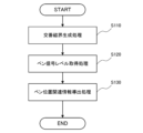
- the position detector 1 selects one TX sensor coil from the TX sensor coil group (first sensor coil group) 100 that generates the transmission magnetic field by switching using the switch 11, and drives the selected TX sensor coil by the TX circuit 10 to emit the transmission magnetic field (step S110).
- FIG. 1A shows a state in which the TX sensor coil T1 is selected.
- the position detector 1 acquires the level of the pen signal at the location of all the RX sensor coils after a certain transmission period, ie a period during which a certain energy would be accumulated if the pen was in the vicinity of the TX sensor coils.
- the position detector 1 detects the level values (33, 105, 118, 121, 110 in the figure) of the pen signal in the area where the TX sensor coil T1 and the RX sensor coils R1, R2, . . . R4 cross (hereinafter, coil cross point area).
- the position detector 1 obtains two-dimensional heat map data RXdata from the signal levels at each coil cross point by sequentially switching the selection of the TX sensor coils (step S120).
- the position detector 1 After acquiring the two-dimensional heat map data RXdata, the position detector 1 executes a coordinate processing process to obtain the pen coordinates, pen tilt (angle from the normal to the sensor surface) or pen orientation (tilt angle) based on the two-dimensional heat map data RXdata (step S130).
- the position detector 1 executes the following steps: a first step of generating an alternating magnetic field from a plurality of conductors arranged in parallel in a first direction of the sensor; a second step of acquiring the level of a pen signal, which is a response alternating magnetic field from the pen stored by the alternating magnetic field, using a plurality of electrodes arranged in parallel in at least a second direction intersecting the first direction; and a third step of deriving information regarding the position of the pen using a two-dimensional distribution of the level of the pen signal at each intersection between the plurality of conductors arranged in parallel in the first direction of the sensor and the plurality of electrodes arranged in parallel in a second direction intersecting the first direction.
- the position detector 1 of this embodiment uses multiple conductors (e.g., TX sensor coils T0, T1, ..., T4) arranged in parallel in a first direction of the sensor only to generate an alternating magnetic field, and uses multiple electrodes (e.g., RX sensor coils R0, R1, ..., R4) arranged in parallel in a second direction intersecting the first direction only to detect the level of the pen signal, and derives information regarding the position of the pen using a two-dimensional distribution of the level of the pen signal at each intersection of the multiple conductors arranged in parallel in the first direction of the sensor and the multiple electrodes arranged in parallel in the second direction intersecting the first direction. Therefore, by using the two-dimensional distribution of the pen signal levels, the accuracy of deriving the coordinates can be improved even when the position indicator is tilted in an oblique direction.
- TX sensor coils T0, T1, ..., T4 uses multiple electrodes (e.g., RX sensor coils R0, R1, ..., R4)
- information about the position of the pen includes either the inclination of the pen with respect to the normal to the sensor plane or the direction of the inclination of the pen with respect to the sensor plane.
- the position detector 1 of this embodiment uses the two-dimensional distribution of the pen signal levels to accurately derive not only the coordinate information of the pen tip, but also the inclination of the pen with respect to the normal to the sensor plane or the direction of the inclination of the pen with respect to the sensor plane. Therefore, even if the position indicator is tilted in an oblique direction, the accuracy of deriving the coordinates can be improved.
- the position detector 1 derives either the inclination of the pen with respect to the normal to the sensor plane or the direction of the inclination of the pen with respect to the sensor plane based on the asymmetry of the two-dimensional distribution.
- the position detector 1 of this embodiment derives the inclination of the pen with respect to the normal to the sensor plane or the direction of the inclination of the pen with respect to the sensor plane based on the asymmetry of the two-dimensional distribution, so that not only the coordinate information of the pen tip, but also the inclination of the pen with respect to the normal to the sensor plane or the direction of the inclination of the pen with respect to the sensor plane can be accurately derived. Therefore, even if the position indicator is tilted in an oblique direction, the accuracy of deriving the coordinates can be improved.
- the position detector 1 acquires a first reference position which is a position indicated by the tip of a pen, and acquires a second reference position which is convex upward or convex downward. The position detector 1 then derives the direction of inclination of the pen with respect to the sensor plane based on the direction of the second reference position with respect to the first reference position.
- the position detector 1 of this embodiment acquires a first reference position, which is the indicated position of the pen tip, and a second reference position, which is convex upward or convex downward, and derives the direction of tilt of the pen relative to the sensor plane based on the direction of the second reference position relative to the first reference position, so that not only the coordinate information of the pen tip, but also the direction of tilt of the pen relative to the sensor plane can be derived with high accuracy. Therefore, even if the position indicator is tilted in an oblique direction, the accuracy of deriving the coordinates can be improved.
- the position detector 1 is composed of a TX circuit 10, a switch 11, a switch 21, a TX sensor coil group (first sensor coil group) 100, an RX sensor coil group (second sensor coil group) 200, an RX circuit 20A, and peripheral circuits such as an amplifier.
- a TX circuit 10 a switch 11, a switch 21, a TX sensor coil group (first sensor coil group) 100, an RX sensor coil group (second sensor coil group) 200, an RX circuit 20A, and peripheral circuits such as an amplifier.
- peripheral circuits such as an amplifier.
- the RX circuit 20A functions as a pen signal level acquisition unit that receives a signal from the RX sensor coil group (second sensor coil group) 200 via the switch 21 and acquires the level of the pen signal, which is a response alternating magnetic field from the position indicator stored by the alternating magnetic field. That is, the RX sensor coils R0, R1, . . . , R4 are connected to the RX circuit 20A and used to detect the pen signal, but are not used to generate the transmitted magnetic field.
- the RX circuit 20A derives either the tilt of the pen relative to the normal to the sensor plane or the direction of the tilt of the pen relative to the sensor plane based on the asymmetry of the two-dimensional distribution.
- the RX circuit 20A also derives the inclination of the pen with respect to the normal to the sensor plane based on the level intensity of the pen signal at the first reference position and the level intensity of the pen signal at the second reference position.
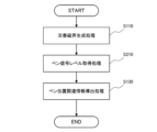
- the position detector 1A selects one TX sensor coil from the TX sensor coil group (first sensor coil group) 100 that generates the transmission magnetic field by switching using the switch 11, and drives the selected TX sensor coil by the TX circuit 10 to emit the transmission magnetic field (step S110).
- FIG. 8 shows a state in which the TX sensor coil T1 is selected.
- the position detector 1A controls the switch 21 after a certain transmission period, i.e., after a period during which a certain amount of energy would be accumulated if a pen were in the vicinity of the TX sensor coil, to select an RX sensor coil for detecting the pen signal, and obtains the level of the pen signal at the position of the selected RX sensor coil.
- FIG. 8 shows a state in which the RX sensor coil R2 is selected.
- the position detector 1A detects the level value (118 in the figure) of the pen signal in a region where the TX sensor coil T1 and the RX sensor coils R1, R2, . . . R4 cross (hereinafter referred to as a coil cross point region).
- the position detector 1A obtains two-dimensional heat map data RXdata by sequentially fixing the TX sensor coil and switching the selection of the RX sensor coil based on the signal level at each coil cross point (step S210).
- the position detector 1A After acquiring the two-dimensional heat map data RXdata, the position detector 1A executes a coordinate processing process to obtain the pen coordinates, pen tilt (angle from the normal to the sensor surface) or pen orientation (tilt angle) based on the two-dimensional heat map data RXdata (step S130).
- the position detector 1A according to this embodiment provides the same effects as the position detector 1 according to the first embodiment.
- the position detector 1B is composed of a TX circuit 10A, a switch 11, a TX sensor coil group (first sensor coil group) 100, an RX sensor coil group (second sensor coil group) 200, an RX circuit 20, and peripheral circuits such as an amplifier.
- a switch 11 a TX sensor coil group (first sensor coil group) 100
- an RX sensor coil group (second sensor coil group) 200 an RX circuit 20, and peripheral circuits such as an amplifier.
- peripheral circuits such as an amplifier.
- the TX circuit 10A includes an alternating magnetic field generating section 111, a global scan section 112, a scan start position determining section 113, and a scan pattern control section 114.
- the alternating magnetic field generating unit 111 transmits a TX signal to the TX sensor coil group (first sensor coil group) 100 via the switch 11, causing the TX sensor coil group (first sensor coil group) 100 to generate an alternating magnetic field.
- the alternating magnetic field generating unit 111 transmits a TX signal based on a control signal from a scan pattern control unit 114, which will be described later.
- the alternating magnetic field generating unit 111 generates an alternating magnetic field a predetermined number of times using, for example, a plurality of conductors (e.g., a TX sensor coil group (first sensor coil group) 100) arranged in parallel in a first direction of the sensor, while changing the position in the first direction (e.g., the arrangement direction of the TX sensor coil group (first sensor coil group) 100).
- a plurality of conductors e.g., a TX sensor coil group (first sensor coil group) 100
- first direction of the sensor e.g., the arrangement direction of the TX sensor coil group (first sensor coil group) 100
- the scan start position determination unit 113 determines that one of the multiple conductors arranged in a first direction (e.g., the arrangement direction of the TX sensor coil group (first sensor coil group) 100) of the sensor in which the signal level from the pen was the largest is to be the start position.
- the scan start position information determined by the scan start position determination unit 113 is output to a scan pattern control unit 114, which will be described later.
- the scan pattern control unit 114 determines a scan pattern based on the scan start position information, and controls the output timing of the TX signal in the alternating magnetic field generation unit 111 and the switching timing of the switch 11 based on the scan pattern. Specifically, the scan pattern control unit 114 sets the scan pattern so that the scanning order is, for example, as shown in FIG. 11, the conductor adjacent to the conductor having the highest signal level from the pen after the conductor scanned first. In addition, the scan pattern control unit 114 sets the scan pattern, for example, as shown in Figure 11, so that the scanning order is the conductor adjacent to the conductor with the highest signal level from the pen after the first scanned conductor, and the conductors are selected sequentially so as to cross the first scanned conductor.
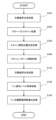
- the alternating magnetic field generating unit 111 generates an alternating magnetic field a predetermined number of times using, for example, a plurality of conductors (for example, the TX sensor coil group (first sensor coil group) 100) arranged in parallel in a first direction of the sensor while changing the position in the first direction (for example, the arrangement direction of the TX sensor coil group (first sensor coil group) 100) (step S310).
- a plurality of conductors for example, the TX sensor coil group (first sensor coil group) 100
- first direction of the sensor for example, the arrangement direction of the TX sensor coil group (first sensor coil group) 100
- the global scan unit 112 acquires the level of the pen signal, which is, for example, a response alternating magnetic field from the pen stored by the alternating magnetic field, at each of a predetermined number of times (step S320).
- the scan start position determination unit 113 determines that the start position is one of the multiple conductors arranged in the arrangement direction of the first direction (e.g., the TX sensor coil group (first sensor coil group)) 100 of the sensor in which the signal level from the pen was the largest (step S330).
- the first direction e.g., the TX sensor coil group (first sensor coil group)
- the scan pattern control unit 114 sets the scan pattern, for example, so that the scan order is the conductor adjacent to the conductor having the highest signal level from the pen after the conductor scanned first. In addition, the scan pattern control unit 114 sets the scan pattern, for example, so that the scanning order is the conductor adjacent to the conductor with the highest signal level from the pen after the first scanned conductor, and the conductors are selected sequentially so as to cross the first scanned conductor (step S340).
- the position detector 1B of this embodiment uses a plurality of conductors (e.g., the TX sensor coil group (first sensor coil group) 100) arranged in parallel in a first direction of the sensor to generate an alternating magnetic field a predetermined number of times while changing the position in the first direction, acquires the level of the pen signal, which is a response alternating magnetic field from the pen stored by the alternating magnetic field, for each of the predetermined number of times, and determines the scanning order for the next predetermined number of times so that the starting position is one of the plurality of conductors arranged in parallel in the first direction of the sensor which had the largest level of the signal from the pen.
- a plurality of conductors e.g., the TX sensor coil group (first sensor coil group) 100
- the position detector 1B performs a global scan using the global scanning unit 112, and determines the order of the next specified number of scans so that the starting position is one of the multiple conductors arranged in parallel in the first direction of the sensor that had the largest signal level from the pen. This is based on the knowledge that when obtaining position information of a pen or the like that moves quickly, if it takes a long time to drive the sensor, blurring of the obtained data occurs. Specifically, it is known that when writing or drawing with a pen at high speed, the coordinate precision deteriorates and the drawn lines become wavy.
- FIG. 13A is a diagram showing an ideal distribution of pen signal levels
- FIG. 13B is a diagram showing the distribution of pen signal levels acquired by position detector 1B according to this embodiment. As can be seen from these figures, the distribution of pen signal levels acquired by the position detector 1B according to this embodiment shows results that compare favorably with the ideal distribution of pen signal levels.
- the position detector 1B changes the scanning order to the conductor adjacent to the conductor having the highest level of the signal from the pen, next to the conductor scanned first.
- the important information in coordinate calculation is the data with the greatest signal strength directly under the pen, and the more distant the data is from that point, the less relevant it is to coordinate calculation. Therefore, by adopting a scan pattern that scans the conductors in order from closest to the pen, it is possible to reduce the fluctuation of data that is weighted in coordinate calculations and suppress deterioration of coordinate accuracy.
- FIG. 13A is a diagram showing an ideal distribution of pen signal levels
- FIG. 13B is a diagram showing the distribution of pen signal levels acquired by position detector 1B according to this embodiment. As can be seen from these figures, the distribution of pen signal levels acquired by the position detector 1B according to this embodiment shows results that compare favorably with the ideal distribution of pen signal levels.
- the position detector 1B sequentially selects the conductor adjacent to the conductor having the highest signal level from the pen after the previously scanned conductor, and so on, straddling the previously scanned conductor.
- the important information in coordinate calculation is the data with the greatest signal strength directly under the pen, and the more distant the data is from that point, the less relevant it is to coordinate calculation. Therefore, by changing the scanning order to the conductor adjacent to the conductor with the highest signal level from the pen after the first scanned conductor and sequentially selecting the conductor so as to cross the first scanned conductor, it is possible to reduce the fluctuation of weighted data in coordinate calculations and suppress deterioration of coordinate accuracy.
- FIG. 13A is a diagram showing an ideal distribution of pen signal levels
- FIG. 13A is a diagram showing an ideal distribution of pen signal levels
- 13B is a diagram showing the distribution of pen signal levels acquired by position detector 1B according to this embodiment. As can be seen from these figures, the distribution of pen signal levels acquired by the position detector 1B according to this embodiment shows results that compare favorably with the ideal distribution of pen signal levels.
- the position detector 1B has been described as an example, but the present invention can also be applied to, for example, a conventional position detector shown in FIG.
- the position detector 1C is composed of a TX circuit 10B, a switch 11, a TX sensor coil group (first sensor coil group) 100, an RX sensor coil group (second sensor coil group) 200, an RX circuit 20, and peripheral circuits such as an amplifier.
- a switch 11 a TX sensor coil group (first sensor coil group) 100
- an RX sensor coil group (second sensor coil group) 200 an RX circuit 20, and peripheral circuits such as an amplifier.
- peripheral circuits such as an amplifier.
- the TX circuit 10B includes an alternating magnetic field generating section 111, a global scan section 112, a scan start position determining section 113, and a scan pattern control section 114A.
- the components having the same reference numerals as those in the third embodiment have the same functions, detailed description thereof will be omitted.
- the scan pattern control unit 114A determines a scan pattern based on the scan start position information, and controls the output timing of the TX signal in the alternating magnetic field generation unit 111 and the switching timing of the switch 11 based on the scan pattern. Specifically, the scan pattern control unit 114A sets the scan pattern, for example, so that the scan order is the conductor adjacent to the conductor having the highest signal level from the pen after the conductor scanned first. In addition, the scan pattern control unit 114A sets the scan pattern, for example, as shown in Figure 15, so that the scanning order is the conductor adjacent to the conductor with the highest signal level from the pen after the first scanned conductor, and the conductors are selected sequentially so as to cross the first scanned conductor.
- the scan pattern control unit 114A when the scanning area exceeds the arrangement area of multiple conductors arranged in parallel in the first direction of the sensor, for example as shown in FIG. 15, the scan pattern control unit 114A extends the scanning area (for example, y5 and y6 in FIG. 15) to an area beyond the arrangement area.
- each of the RX sensor coils in the RX sensor coil group (second sensor coil group) 200 is connected to the RX circuit 20 via a switch 21, and the other end of each of the RX sensor coils is connected to a reference potential such as GND.
- a differential amplifier circuit is provided in the RX circuit 20, one end and the other end of each of the RX sensor coils in the RX sensor coil group (second sensor coil group) 200 may be connected to the differential amplifier circuit.
- ⁇ Configuration of integrated sensor> 25 to 29 are diagrams for explaining the configuration of a position detector 1E including an integrated sensor (Integrated/Universal Sensor Module) configured by integrating a TX sensor coil group (first sensor coil group) 100 and an RX sensor coil group (second sensor coil group) 200 into a touch sensor.
- This configuration is useful in the case of a stack configuration called on-cell touch, which is provided on the upper side (pen side) of a display 300D as shown in FIG. 22D.
- the TX circuit 10 on the left side of the drawing drives one end of the TX sensor coil electrode T1 selected by the switch 11 with a positive-phase touch signal
- the TX circuit 10 on the right side of the drawing drives the other end of the selected TX sensor coil electrode T1 with a positive-phase touch signal by the switch 11.
- the RX circuit 20 detects a change in mutual capacitance from a reference value at a cross point (the intersection of T1 and TR2) in the selected RX touch electrode TR2.
- the RX circuit 20 acquires the change in capacitance at each cross point as two-dimensional heat map data, and derives the position of the finger touch using calculations used in capacitance detection, such as center of gravity calculations.
- a position detector 1F according to this embodiment will be described with reference to FIGS.
- the configuration of the position detector 1F is similar to that of the position detector 1B according to the third embodiment, and therefore a detailed description thereof will be omitted.
- the position detector 1F has the same hardware configuration, but acquires the level of the pen signal, which is the response alternating magnetic field from the pen, or the signal level corresponding to the capacitive coupling with the finger, and acquires information regarding the position of the pen and the position of the finger.
- the position detector 1F includes a first sensor coil group 100 consisting of a plurality of conductors having a plurality of electrodes arranged in parallel in a first direction, a second sensor coil group 200 consisting of a plurality of conductors having a plurality of electrodes arranged in parallel in a second direction intersecting the first direction, an alternating magnetic field generating unit 111 that generates an alternating magnetic field from the first sensor coil group 100, a signal level acquiring unit (RX circuit 20) that acquires the level of a pen signal, which is a response alternating magnetic field from a position indicator stored by the alternating magnetic field, or a signal level corresponding to capacitive coupling with a finger, using the second sensor coil group 200, and a signal level acquiring unit (RX circuit 20) that acquires the level of the pen signal at each intersection between the plurality of electrodes of the first sensor coil group 100 and the plurality of electrodes of the second sensor coil group 200, or the signal level corresponding to capacitive coupling with a
- the control unit includes an information derivation unit (RX circuit 20) that derives information regarding the position of the pen or finger using the two-dimensional distribution of the alternating magnetic field, and a control unit that controls the operation.
- the control unit causes the alternating magnetic field generating unit 111 to generate an alternating magnetic field a predetermined number of times while changing the position in a first direction using the first sensor coil group 100, causes the signal level acquiring unit (RX circuit 20) to acquire a pen signal level, which is a response alternating magnetic field from the pen stored by the alternating magnetic field, or a signal level corresponding to capacitive coupling with the finger, for each of the predetermined number of times, and determines the scanning order for the next predetermined number of times so that one of the multiple conductors arranged side by side in the first direction of the first sensor coil group 100 that had the largest signal level from the pen or the largest signal level corresponding to capacitive coupling with the finger becomes the starting position.
- RX circuit 20 information derivation unit
- the process of deriving position information of the pen or finger is executed alternately, and in the process of deriving position information of the pen, the alternating magnetic field generation process of the alternating magnetic field generation unit 111 is executed for a period during which a predetermined energy is accumulated in the pen, and then stopped, and after the stoppage, the signal level acquisition process of the signal level acquisition unit (RX circuit 20) is executed to acquire the alternating magnetic field generated by the energy accumulated in the pen, and in the process of deriving position information of the finger, the alternating magnetic field generation process of the alternating magnetic field generation unit 111 and the signal level acquisition process of the signal level acquisition unit (RX circuit 20) are executed continuously within the same period.
- the first sensor coil group 100 becomes a driving coil that generates an alternating magnetic field by the alternating magnetic field generating unit 111
- the second sensor coil group 200 becomes a receiving coil that receives a signal corresponding to capacitive coupling with the finger.
- the second sensor coil group 200 is formed in a U-shape, and in the process of deriving pen position information, each acts as a coil ( Figure 33(A)), and in the process of deriving finger position information, the open part of the U-shape is short-circuited and functions as a single receiving electrode ( Figure 33(B)).
- the scan pattern control unit 114 sets the scan pattern, for example, so that the scan order is the conductor adjacent to the conductor having the highest signal level from the pen after the conductor scanned first. In addition, the scan pattern control unit 114 sets the scan pattern, for example, so that the scanning order is the conductor adjacent to the conductor with the highest signal level from the pen after the first scanned conductor, and the conductors are selected sequentially so as to cross the first scanned conductor (step S340).
- the position detector 1F selects one TX sensor coil from the TX sensor coil group (first sensor coil group) 100 that generates the transmission magnetic field by switching using the switch 11, and drives the selected TX sensor coil using the TX circuit 10 to transmit the transmission magnetic field (step S110).
- the position detector 1F acquires the level of the pen signal at the position of all the RX sensor coils after a certain transmission period, ie a period during which a certain amount of energy would be accumulated if the pen was in the vicinity of the TX sensor coils.
- the position detector 1F detects the level values (33, 105, 118, 121, 110 in the figure) of the pen signal in the area where the TX sensor coil T1 and the RX sensor coils R1, R2, . . . R4 cross (hereinafter, coil cross point area).
- the position detector 1F obtains two-dimensional heat map data RXdata by sequentially switching the selection of the TX sensor coils based on the signal levels at each coil cross point (step S120).
- the alternating magnetic field generating unit 111 generates an alternating magnetic field a predetermined number of times while changing the position in a first direction (e.g., the direction in which the TX sensor coil group (first sensor coil group) 100 are arranged) using, for example, multiple conductors arranged in a first direction of the sensor (e.g., the TX sensor coil group (first sensor coil group) 100) (step S311).
- a first direction e.g., the direction in which the TX sensor coil group (first sensor coil group) 100 are arranged
- multiple conductors arranged in a first direction of the sensor e.g., the TX sensor coil group (first sensor coil group) 100
- the global scan unit 112 acquires a signal level corresponding to the capacitive coupling with the finger each of a predetermined number of times (step S321).
- the scan start position determination unit 113 determines that the start position is one of the multiple conductors arranged in the arrangement direction of the first direction of the sensor (e.g., the TX sensor coil group (first sensor coil group)) 100 where the signal level corresponding to the capacitive coupling with the finger is the largest, i.e., where it is estimated that a finger is present (step S331).
- the first direction of the sensor e.g., the TX sensor coil group (first sensor coil group)
- the position detector 1F selects one TX sensor coil from the TX sensor coil group (first sensor coil group) 100 that generates the transmission magnetic field by switching using the switch 11 according to the processing result of step S340, and drives the selected TX sensor coil using the TX circuit 10 to transmit the transmission magnetic field (step S351).
- the position detector 1F obtains signal levels corresponding to the capacitive coupling with the finger at the positions of all RX sensor coils during the period in which the position detector 1F obtains the finger position information.
- the position detector 1F detects signal level values (33, 105, 118, 121, 110 in the figure) corresponding to capacitive coupling with a finger in a region where the TX sensor coil T1 and the RX sensor coils R1, R2, . . . R4 cross (hereinafter referred to as a coil cross point region).
- the position detector 1F obtains two-dimensional heat map data RXdata by sequentially switching the selection of the TX sensor coils based on the signal levels at each coil cross point (step S120).
- the position detector 1F includes the first sensor coil group 100 consisting of a plurality of conductors having a plurality of electrodes arranged in parallel in a first direction, the second sensor coil group 200 consisting of a plurality of conductors having a plurality of electrodes arranged in parallel in a second direction intersecting the first direction, an alternating magnetic field generating unit 111 that generates an alternating magnetic field from the first sensor coil group 100, a signal level acquiring unit (RX circuit 20) that acquires, using the second sensor coil group 200, the level of a pen signal which is a response alternating magnetic field from a position indicator stored by the alternating magnetic field or a signal level corresponding to capacitive coupling with a finger, and a signal level acquiring unit (RX circuit 20) that acquires the level of the pen signal at each intersection between the plurality of electrodes of the first sensor coil group 100 and the plurality of electrodes of the second sensor coil group 200 or the level of a signal
- the control unit includes an information derivation unit (RX circuit 20) that derives information regarding the position of the pen or finger using the two-dimensional distribution of the signal level obtained by scanning the first sensor coil group 100, and a control unit that controls the operation.
- the control unit causes the alternating magnetic field generating unit 111 to generate an alternating magnetic field a predetermined number of times while changing the position in the first direction, using the first sensor coil group 100, and causes the signal level acquiring unit (RX circuit 20) to acquire a pen signal level, which is a response alternating magnetic field from the pen stored by the alternating magnetic field, or a signal level corresponding to capacitive coupling with the finger, for each of the predetermined number of times, and determines the scanning order for the next predetermined number of times so that one of the multiple conductors arranged side by side in the first direction of the first sensor coil group 100 that had the largest signal level from the pen or the largest signal level corresponding to capacitive coupling with the finger becomes the starting position.
- RX circuit 20 information derivation unit
- the position detector 1F of this embodiment performs a global scan and determines the order of the next specified number of scans so that the starting position is one of the multiple conductors arranged in parallel in the first direction of the sensor that has the largest signal level from the pen or the largest signal level corresponding to capacitive coupling with the finger.
- This is based on the knowledge that when obtaining position information of a fast-moving pen, finger, or the like, if it takes a long time to drive the sensor, blurring of the obtained data will occur. Specifically, it is known that when writing or drawing with a pen at high speed, the coordinate precision deteriorates and the drawn lines become wavy.
- the important information in coordinate calculation is the data with the greatest signal strength directly under the pen or finger, and the more distant the data is from that point, the less relevant it is to coordinate calculation. Therefore, the accuracy of deriving the coordinates can be improved by determining the order of the next specified number of scans so that the starting position is one of the multiple conductors arranged in parallel in the first direction of the sensor that has the largest signal level from the pen or the largest signal level corresponding to capacitive coupling with the finger.
- the accuracy of deriving the coordinates can be improved. Furthermore, with the same hardware configuration, it is possible to execute control according to its characteristics, and since it is possible to obtain pen coordinate information and finger coordinate information, it is possible to detect highly accurate coordinate information while reducing costs.
- the process of deriving the position information of the pen or finger is executed alternately, and in the process of deriving the position information of the pen, the alternating magnetic field generation process of the alternating magnetic field generation unit 111 is executed until a period during which a predetermined energy is accumulated in the pen, and then stopped, and after the stoppage, the signal level acquisition process of the signal level acquisition unit (RX circuit 20) is executed to acquire the alternating magnetic field generated by the energy accumulated in the pen, and in the process of deriving the position information of the finger, the alternating magnetic field generation process of the alternating magnetic field generation unit 111 and the signal level acquisition process of the signal level acquisition unit (RX circuit 20) are executed continuously within the same period.
- the process of deriving the position information of the pen or finger is executed alternately, and in the process of deriving the position information of the pen, the alternating magnetic field generation process of the alternating magnetic field generation unit 111 is executed until a period during which a predetermined energy is accumulated in the pen, and then stopped, and after the stoppage, the signal level acquisition process of the signal level acquisition unit (RX circuit 20) is executed to acquire the alternating magnetic field generated by the energy accumulated in the pen, and in the process of deriving the position information of the finger, the alternating magnetic field generation process of the alternating magnetic field generation unit 111 and the signal level acquisition process of the signal level acquisition unit (RX circuit 20) are executed continuously within the same period. Since it is possible to execute control according to the characteristics of the hardware using the same configuration, it is possible to detect highly accurate coordinate information while reducing costs.
- the first sensor coil group 100 serves as a driving coil that generates an alternating magnetic field by the alternating magnetic field generating unit 111
- the second sensor coil group 200 serves as a receiving coil that receives a signal corresponding to capacitive coupling with the finger.
- the second sensor coil group 200 is formed in a U-shape, and in the process of deriving pen position information, each acts as a coil ( Figure 33 (A)), and in the process of deriving finger position information, the open part of the U-shape is short-circuited and functions as a single receiving electrode ( Figure 33 (B)). That is, in detecting finger position information, if the coil has a U-shape, the length of the conductor wire forming the coil becomes long, and the resulting capacitance reduces the detection sensitivity. However, in the position detector 1F according to this embodiment, the open portion of the U-shape is short-circuited and functions as one receiving electrode, so that the detection sensitivity does not decrease. Therefore, it is possible to detect highly accurate coordinate information while reducing costs.
- the processing of the TX circuits 10, 10A, 10B, 10C, and 10D can be recorded on a recording medium that can be read by a computer system, and the program recorded on this recording medium can be read and executed by the TX circuits 10, 10A to 10E, thereby realizing the position detectors 1, 1A to 1E of the present invention.
- the computer system here includes hardware such as the OS and peripheral devices.
- the "computer system” also includes the homepage providing environment (or display environment).
- the above program may be transmitted from a computer system in which the program is stored in a storage device or the like to another computer system via a transmission medium, or by transmission waves in the transmission medium.
- the "transmission medium” that transmits the program refers to a medium that has the function of transmitting information, such as a network (communication network) such as the Internet or a communication line (communication line) such as a telephone line.
- the above program may also be one that realizes some of the functions described above. Furthermore, it may be one that realizes the functions described above in combination with a program that is already recorded in the computer system, a so-called differential file (differential program).
- a first sensor coil group including a plurality of conductors having a plurality of electrodes arranged in parallel in a first direction; and a second sensor coil group including a plurality of conductors having a plurality of electrodes arranged in parallel in a second direction intersecting the first direction;
- the one or more processors : an alternating magnetic field generating unit that generates an alternating magnetic field from the first sensor coil group; a pen signal level acquiring unit that acquires a level of a pen signal, which is a response alternating magnetic field from a position indicator stored by the alternating magnetic field, using the second sensor coil group; an information derivation unit that derives information about a position of the position indicator by using a two-dimensional distribution of levels of the pen signal at each of the intersections between a plurality of conductive wires of the first sensor coil group and a plurality of electrodes of the second sensor coil group; including a position detector.
- a first sensor coil group including a plurality of conductors having a plurality of electrodes arranged in parallel in a first direction; and a second sensor coil group including a plurality of conductors having a plurality of electrodes arranged in parallel in a second direction intersecting the first direction;
- the one or more processors : an alternating magnetic field generating unit that generates an alternating magnetic field from the first sensor coil group; a pen signal level acquiring unit that acquires a level of a pen signal, which is a response alternating magnetic field from a position indicator stored by the alternating magnetic field, using the second sensor coil group; an information derivation unit that derives information about a position of the position indicator by using a two-dimensional distribution of levels of the pen signal at each of the intersections between a plurality of conductive wires of the first sensor coil group and a plurality of electrodes of the second sensor coil group;
Landscapes
- Engineering & Computer Science (AREA)
- General Engineering & Computer Science (AREA)
- Theoretical Computer Science (AREA)
- Physics & Mathematics (AREA)
- Human Computer Interaction (AREA)
- General Physics & Mathematics (AREA)
- Electromagnetism (AREA)
- Measurement Of Length, Angles, Or The Like Using Electric Or Magnetic Means (AREA)
- Position Input By Displaying (AREA)
Abstract
Description
この位置入力装置は、ペン形状の位置指示器(ペン型位置指示器)と、このペン型位置指示器を用いて、ポインティング操作や文字及び図等の入力を行う入力面を有する位置検出装置と、から構成されている。
一方、位置検出装置は、図34に示すように、アクティブエリアAA内における位置指示器のX軸方向の座標を求めるために、
X方向に並べられたXセンサコイルX0、・・・、X4を含むXセンサコイル群と、
Xセンサコイル群に接続されたスイッチと、
・送出期間ではX軸に並べられたXセンサコイル群の各々に電流を流すことで交番磁界(送出磁界、以下同じ)を生成し、
・送出期間の後の検出期間では、送出期間に共振回路にエネルギーを蓄えた位置指示器からその後も継続的に生成されるペン信号(位置指示器の回路により生成される交番磁界、以下同じ)によりXセンサコイル群の各々に生じる起電力を電流または電圧により検出するX軸TX/RX回路と、
を含み構成される。
Y方向に並べられたYセンサコイルY0、・・・、Y4を含むYセンサコイル群と、
Yセンサコイル群に接続されたスイッチと、
・送出期間ではY軸に並べられたXセンサコイル群の各々に電流を流すことで送出磁界を生成し、
・送出期間の後の検出期間では、送出期間に共振回路にエネルギーを蓄えた位置指示器からその後も継続的に生成されるペン信号によりYセンサコイル群の各々に生じる起電力を電流または電圧により検出する、Y軸TX/RX回路と、
を含み構成される。
一方で、位置検出装置は、送信に用いたセンサコイルを受信回路に接続して位置指示器の共振回路から送信される信号を受信する。
位置検出装置は、センサコイルを順次に切り替えて、このような信号の送受信を行うことによって、位置検出装置上における位置指示器の位置を検出する。
図1から図7を用いて、本実施形態に係る位置検出器1について説明する。
位置検出器1は、図1に示すように、TX回路10と、スイッチ11と、TXセンサコイル群(第1のセンサコイル群)100と、RXセンサコイル群(第2のセンサコイル群)200と、RX回路20と、及び増幅器などの周辺回路により構成されている。
また、TXセンサコイル群(第1のセンサコイル群)100を構成するTXセンサコイルは、例えば、等間隔に並んで配置されている。
また、RXセンサコイル群(第2のセンサコイル群)200を構成するRXセンサコイルは、例えば、等間隔に並んで配置されている。
つまり、本実施形態に係る位置検出器1では、TXセンサコイルT0、T1、・・・、T4は、TX回路10に接続され交番磁界を生成するために用いられるが、ペン信号の検出には、用いられない。
つまり、RXセンサコイルR0、R1、・・・、R4は、RX回路20に接続されペン信号を検出するために用いられるが、送出磁界の生成には用いられない。
また、RX回路20は、TXセンサコイル群(第1のセンサコイル群)100の複数の導線とRXセンサコイル群(第2のセンサコイル群)200の複数の電極との各々の交点におけるペン信号のレベルの二次元分布を用いて、位置指示器の位置に関する情報を導出する情報導出部として機能する。
ここで、ペン(位置指示器)の位置に関する情報には、センサ平面(X軸とY軸とからなるXY平面)の法線に対するペンの傾きあるいは、センサ平面に対するペンの傾きの方向のいずれかを含む。
図2Aでは、(TX6、RX7)において、図2Bでは、(MATX6、MARX7)において、ピークの値を示し、同心円状に同じようなペン信号のレベルの変化が見られ、図2Cも同様の状態を示している。
図2Aおよび図2Bから、(TX6、RX7)あるいは(MATX6、MARX7)がペンのペン先の指示位置である第1の参照位置である。
この場合のセンサ平面の法線に対するペンの傾き(チルト角)、センサ平面に対するペンの傾きの方向(アングル角)についての導出方法は、従来例と同様であるため詳細は省略する。
図3Aでは、(TX6、RX7)において、図3Bでは、(MATX6、MARX7)において、ピークの値を示し、ここから、上方に向かう方向でペン信号のレベルの変化が著しくなっており、図3Cも同様の状態を示している。
図3Aおよび図3Bから、(TX6、RX7)あるいは(MATX6、MARX7)がペンのペン先の指示位置である第1の参照位置である。
この場合のセンサ平面の法線に対するペンの傾き(チルト角)、センサ平面に対するペンの傾きの方向(アングル角)についての導出方法は、従来例と同様であるため詳細は省略する。
図4Aでは、(TX6、RX7)において、図4Bでは、(MATX6、MARX7)において、ピークの値を示し、ここから、右に向かう方向でペン信号のレベルの変化が著しくなっており、図4Cも同様の状態を示している。
図4Aおよび図4Bから、(TX6、RX7)あるいは(MATX6、MARX7)がペンのペン先の指示位置である第1の参照位置である。
この場合のセンサ平面の法線に対するペンの傾き(チルト角)、センサ平面に対するペンの傾きの方向(アングル角)についての導出方法は、従来例と同様であるため詳細は省略する。
図5Bでは、(MATX6、MARX7)において、ピークの値を示しており、このポイントがペンのペン先の指示位置である第1の参照位置である。
また、図5Bでは、(MATX9、MARX9)において、第2のピークの値を示しており、このポイントが第2の参照位置となる。
そして、RX回路20の情報導出部は、ペンのペン先の指示位置である第1の参照位置を取得し、上に凸あるいは下に凸となる第2の参照位置を取得して、第1の参照位置に対する第2の参照位置の方向に基づいて、センサ平面に対するペンの傾きの方向を導出する。
図6Bでは、(MATX6、MARX7)において、ピークの値を示しており、このポイントがペンのペン先の指示位置である第1の参照位置である。
また、図6Bでは、(MATX9、MARX4)において、第2のピークの値を示しており、このポイントが第2の参照位置となる。
そして、RX回路20の情報導出部は、ペンのペン先の指示位置である第1の参照位置を取得し、上に凸あるいは下に凸となる第2の参照位置を取得して、第1の参照位置に対する第2の参照位置の方向に基づいて、センサ平面に対するペンの傾きの方向を導出する。
図7を用いて、本実施形態に係る位置検出器1の処理について説明する。
図1Aにおいては、TXセンサコイルT1が選択された状態を示している。
位置検出器1は、TXセンサコイルT1とRXセンサコイルR1、R2・・・R4とがクロスする領域(以下、コイルクロスポイント領域)におけるペン信号のレベル値(図中33、105、118、121、110)を検出する。
位置検出器1は、各々のコイルクロスポイントでの信号レベルを、順次TXセンサコイルの選択を切り替えることによって、2次元ヒートマップデータRXdataを得る(ステップS120)。
以上、説明したように、本実施形態に係る位置検出器1において、位置検出器1は、センサの第1の方向に並設された複数の導線から交番磁界を生成する第1の工程と、少なくとも第1の方向と交差する第2の方向に並設された複数の電極を用いて、交番磁界によって蓄えられたペンからの応答交番磁界であるペン信号のレベルを取得する第2の工程と、センサの第1の方向に並設された複数の導線と第1の方向と交差する第2の方向に並設された複数の電極との各々の交点におけるペン信号のレベルの二次元分布を用いて、ペンの位置に関する情報を導出する第3の工程と、を実行する。
つまり、本実施形態に係る位置検出器1は、センサの第1の方向に並設された複数の導線(例えば、TXセンサコイルT0、T1、・・・、T4)を交番磁界の生成ためにだけ用い、第1の方向と交差する第2の方向に並設された複数の電極(例えば、RXセンサコイルR0、R1、・・・、R4)をペン信号のレベルのみを検出するために用い、センサの第1の方向に並設された複数の導線と第1の方向と交差する第2の方向に並設された複数の電極との各々の交点におけるペン信号のレベルの二次元分布を用いて、ペンの位置に関する情報を導出する。
そのため、ペン信号のレベルの二次元分布を用いることにより、位置指示器が斜め方向に傾いた場合であっても、座標の導出精度を向上させることができる。
つまり、本実施形態に係る位置検出器1は、ペン信号のレベルの二次元分布を用いることにより、ペンのペン先の座標情報は、もとより、センサ平面の法線に対するペンの傾きあるいは、センサ平面に対するペンの傾きの方向も精度よく導出する。
そのため、位置指示器が斜め方向に傾いた場合であっても、座標の導出精度を向上させることができる。
つまり、本実施形態に係る位置検出器1は、二次元分布の非対称性に基づいて、センサ平面の法線に対するペンの傾きまたはセンサ平面に対するペンの傾きの方向を導出するため、ペンのペン先の座標情報は、もとより、センサ平面の法線に対するペンの傾きあるいは、センサ平面に対するペンの傾きの方向も精度よく導出することができる。
そのため、位置指示器が斜め方向に傾いた場合であっても、座標の導出精度を向上させることができる。
そして、位置検出器1は、第1の参照位置に対する第2の参照位置の方向に基づいて、センサ平面に対するペンの傾きの方向を導出する。
つまり、本実施形態に係る位置検出器1は、ペンのペン先の指示位置である第1の参照位置および、上に凸あるいは下に凸となる第2の参照位置を取得し、第1の参照位置に対する第2の参照位置の方向に基づいて、センサ平面に対するペンの傾きの方向を導出するため、ペンのペン先の座標情報は、もとより、センサ平面に対するペンの傾きの方向についても精度よく導出することができる。
そのため、位置指示器が斜め方向に傾いた場合であっても、座標の導出精度を向上させることができる。
つまり、本実施形態に係る位置検出器1は、第1の参照位置におけるペン信号のレベル強度と、第2の参照位置におけるペン信号のレベル強度と、に基づいて、センサ平面の法線に対するペンの傾きを導出するため、ペンのペン先の座標情報は、もとより、センサ平面の法線に対するペンの傾きについても精度よく導出することができる。
そのため、位置指示器が斜め方向に傾いた場合であっても、座標の導出精度を向上させることができる。
そのため、位置検出器1の回路構成を簡素化することができる。
本実施形態においては、位置検出器1のRX回路20は、RXセンサコイル群(第2のセンサコイル群)200の複数の電極を用いて、交番磁界によって蓄えられた位置指示器からの応答交番磁界であるペン信号を受信し、ペン信号のレベルを取得するとしたが、RX回路20が有するRXチャネル数に応じてRXセンサコイル群(第2のセンサコイル群)200に含まれるRXセンサコイル全部を用いて同時に検出するとしてもよいし、一部の複数のRXセンサコイルを同時に検出するとしてもよい。
図8、図9を用いて、本実施形態に係る位置検出器1Aについて説明する。
位置検出器1は、図8に示すように、TX回路10と、スイッチ11と、スイッチ21と、TXセンサコイル群(第1のセンサコイル群)100と、RXセンサコイル群(第2のセンサコイル群)200と、RX回路20Aと、及び増幅器などの周辺回路により構成されている。
なお、第1の実施形態と同一の符号を付す構成要素については、同様の機能を有することから、その詳細な説明は、省略する。
つまり、RXセンサコイルR0、R1、・・・、R4は、RX回路20Aに接続されペン信号を検出するために用いられるが、送出磁界の生成には用いられない。
また、RX回路20Aは、TXセンサコイル群(第1のセンサコイル群)100の複数の導線とRXセンサコイル群(第2のセンサコイル群)200の複数の電極との各々の交点におけるペン信号のレベルの二次元分布を用いて、位置指示器の位置に関する情報を導出する情報導出部として機能する。
ここで、ペン(位置指示器)の位置に関する情報には、センサ平面(X軸とY軸とからなるXY平面)の法線に対するペンの傾きあるいは、センサ平面に対するペンの傾きの方向のいずれかを含む。
図9を用いて、本実施形態に係る位置検出器1Aの処理について説明する。
図8においては、TXセンサコイルT1が選択された状態を示している。
図8においては、RXセンサコイルR2が選択された状態を示している。
位置検出器1Aは、TXセンサコイルT1とRXセンサコイルR1、R2・・・R4とがクロスする領域(以下、コイルクロスポイント領域)におけるペン信号のレベル値(図中118)を検出する。
位置検出器1Aは、各々のコイルクロスポイントでの信号レベルを、順次TXセンサコイルを固定し、RXセンサコイルの選択を切り替えることによって、2次元ヒートマップデータRXdataを得る(ステップS210)。
以上、説明したように、本実施形態に係る位置検出器1Aにおいては、第1の実施形態に係る位置検出器1と同様の作用効果を奏する。
図10から図13を用いて、本実施形態に係る位置検出器1Bについて説明する。
位置検出器1Bは、TX回路10Aと、スイッチ11と、TXセンサコイル群(第1のセンサコイル群)100と、RXセンサコイル群(第2のセンサコイル群)200と、RX回路20と、及び増幅器などの周辺回路により構成されている。
なお、第1の実施形態および第2の実施形態と同一の符号を付す構成要素については、同様の機能を有することから、その詳細な説明は、省略する。
TX回路10Aは、図10に示すように、交番磁界生成部111と、グローバルスキャン部112と、スキャン開始位置決定部113と、スキャンパターン制御部114と、を含んで構成されている。
交番磁界生成部111は、後述するスキャンパターン制御部114からの制御信号に基づいて、TX信号を送信する。
具体的には、交番磁界生成部111は、例えば、センサの第1の方向に並設された複数の導線(例えば、TXセンサコイル群(第1のセンサコイル群)100)を用いて、所定回数の交番磁界を第1の方向(例えば、TXセンサコイル群(第1のセンサコイル群)100の並設方向)での位置を変更しながら生成する。
具体的には、グローバルスキャン部112は、例えば、交番磁界により蓄えられたペンからの応答交番磁界であるペン信号のレベルを所定回数の各々で取得する。
グローバルスキャン部112による検出結果は、後述するスキャン開始位置決定部113に出力される。
スキャン開始位置決定部113において決定されたスキャン開始位置情報は、後述するスキャンパターン制御部114に出力される。
具体的には、スキャンパターン制御部114は、例えば、図11に示すように、スキャン順を先にスキャンした導線の次にペンからの信号のレベルが最も大きかった導線に隣接する導線とするように、スキャンパターンを設定する。
また、スキャンパターン制御部114は、例えば、図11に示すように、スキャン順を先にスキャンした導線の次にペンからの信号のレベルが最も大きかった導線に隣接する導線とし、先にスキャンした導線を跨ぐように順次選択するように、スキャンパターンを設定する。
図12を用いて、本実施形態に係る位置検出器1Bの処理について説明する。
また、スキャンパターン制御部114は、例えば、スキャン順を先にスキャンした導線の次にペンからの信号のレベルが最も大きかった導線に隣接する導線とし、先にスキャンした導線を跨ぐように順次選択するように、スキャンパターンを設定する(ステップS340)。
以上、説明したように、本実施形態に係る位置検出器1Bは、センサの第1の方向に並設された複数の導線(例えば、TXセンサコイル群(第1のセンサコイル群)100)を用いて、所定回数の交番磁界を第1の方向での位置を変更しながら生成し、交番磁界により蓄えられたペンからの応答交番磁界であるペン信号のレベルを所定回数の各々で取得し、次の所定回数のスキャン順を、ペンからの信号のレベルが最も大きかったセンサの第1の方向に並設された複数の導線のうちの1の導線が開始位置となるように決定する。
つまり、位置検出器1Bは、グローバルスキャン部112によりグローバルスキャンを行い、次の所定回数のスキャン順を、ペンからの信号のレベルが最も大きかったセンサの第1の方向に並設された複数の導線のうちの1の導線が開始位置となるように決定する。
これは、移動速度の早いペン等の位置情報を取得する場合、センサ駆動に時間がかかると取得データにブレが生じるとの知見に基づくものである。
具体的には、高速でペンによる書きこみや描画を行ったときには、座標精度が悪化し、描画した線に波打ちなどが生じることが分かっている。
一方で、座標計算において重要な情報はペンの直下の信号強度の最も大きいデータであり、そこから離れたデータほど座標計算への関与は薄れていく。
そのため、次の所定回数のスキャン順を、ペンからの信号のレベルが最も大きかったセンサの第1の方向に並設された複数の導線のうちの1の導線が開始位置となるように決定することによって、高速でペンによる書きこみや描画を行った場合であって、ペンが斜め方向に傾いた場合であっても、座標の導出精度を向上させることができる。
図13Aは、理想的なペン信号レベルの分布を示した図であり、図13Bは、本実施形態に係る位置検出器1Bにおいて取得されたペン信号レベルの分布を示した図である。
これらの図からも分かるように、本実施形態に係る位置検出器1Bにおいて取得されたペン信号レベルの分布は、理想的なペン信号レベルの分布と遜色ない結果を示している。
上記のように、座標計算において重要な情報はペンの直下の信号強度の最も大きいデータであり、そこから離れたデータほど座標計算への関与は薄れていく。
そのため、ペンに近い導線から順番にスキャンするスキャンパターンを採用することにより、座標計算において重みのあるデータのブレを低減させ、座標精度の悪化を抑制することができる。
図13Aは、理想的なペン信号レベルの分布を示した図であり、図13Bは、本実施形態に係る位置検出器1Bにおいて取得されたペン信号レベルの分布を示した図である。
これらの図からも分かるように、本実施形態に係る位置検出器1Bにおいて取得されたペン信号レベルの分布は、理想的なペン信号レベルの分布と遜色ない結果を示している。
上記のように、座標計算において重要な情報はペンの直下の信号強度の最も大きいデータであり、そこから離れたデータほど座標計算への関与は薄れていく。
そのため、スキャン順を先にスキャンした導線の次にペンからの信号のレベルが最も大きかった導線に隣接する導線とし、先にスキャンした導線を跨ぐように順次選択するにより、座標計算において重みのあるデータのブレを低減させ、座標精度の悪化を抑制することができる。
図13Aは、理想的なペン信号レベルの分布を示した図であり、図13Bは、本実施形態に係る位置検出器1Bにおいて取得されたペン信号レベルの分布を示した図である。
これらの図からも分かるように、本実施形態に係る位置検出器1Bにおいて取得されたペン信号レベルの分布は、理想的なペン信号レベルの分布と遜色ない結果を示している。
上記第3の実施形態においては、位置検出器1Bを例示して説明したが、例えば、図30に示した従来の位置検出装置においても適用することができる。
図14から図17を用いて、本実施形態に係る位置検出器1Cについて説明する。
位置検出器1Cは、TX回路10Bと、スイッチ11と、TXセンサコイル群(第1のセンサコイル群)100と、RXセンサコイル群(第2のセンサコイル群)200と、RX回路20と、及び増幅器などの周辺回路により構成されている。
なお、第1の実施形態から第3の実施形態と同一の符号を付す構成要素については、同様の機能を有することから、その詳細な説明は、省略する。
TX回路10Bは、図14に示すように、交番磁界生成部111と、グローバルスキャン部112と、スキャン開始位置決定部113と、スキャンパターン制御部114Aと、を含んで構成されている。
なお、第3の実施形態と同一の符号を付す構成要素については、同様の機能を有することから、その詳細な説明は、省略する。
具体的には、スキャンパターン制御部114Aは、例えば、スキャン順を先にスキャンした導線の次にペンからの信号のレベルが最も大きかった導線に隣接する導線とするように、スキャンパターンを設定する。
また、スキャンパターン制御部114Aは、例えば、図15に示すように、スキャン順を先にスキャンした導線の次にペンからの信号のレベルが最も大きかった導線に隣接する導線とし、先にスキャンした導線を跨ぐように順次選択するように、スキャンパターンを設定する。
本実施形態において、スキャンパターン制御部114Aは、例えば、図15に示すように、スキャンする領域がセンサの第1の方向に並設された複数の導線の配置領域を超える場合には、配置領域を超えた領域にスキャンする領域(例えば、図15のy5、y6)を拡張する。
図16を用いて、本実施形態に係る位置検出器1Cの処理について説明する。
また、スキャンパターン制御部114Aは、例えば、スキャン順を先にスキャンした導線の次にペンからの信号のレベルが最も大きかった導線に隣接する導線とし、先にスキャンした導線を跨ぐように順次選択するように、スキャンパターンを設定する。
また、スキャンパターン制御部114Aは、例えば、スキャンする領域がセンサの第1の方向に並設された複数の導線の配置領域を超える場合には、配置領域を超えた領域にスキャンする領域を拡張し、スキャンを実行させる(ステップS410)。
以上、説明したように、本実施形態に係る位置検出器1Cは、スキャンする領域がセンサの第1の方向に並設された複数の導線(例えば、TXセンサコイル群(第1のセンサコイル群)100)の配置領域を超える場合には、配置領域を超えた領域にスキャンする領域(例えば、図15のy5、y6)を拡張する。
つまり、位置検出器1Cは、グローバルスキャン部112によりグローバルスキャンを行い、次の所定回数のスキャン順を、ペンからの信号のレベルが最も大きかったセンサの第1の方向に並設された複数の導線のうちの1の導線が開始位置となるように決定する。
これは、移動速度の早いペン等の位置情報を取得する場合、センサ駆動に時間がかかると取得データにブレが生じるとの知見に基づくものである。
具体的には、高速でペンによる書きこみや描画を行ったときには、座標精度が悪化し、描画した線に波打ちなどが生じることが分かっている。
一方で、座標計算において重要な情報はペンの直下の信号強度の最も大きいデータであり、そこから離れたデータほど座標計算への関与は薄れていく。
そのため、次の所定回数のスキャン順を、ペンからの信号のレベルが最も大きかったセンサの第1の方向に並設された複数の導線のうちの1の導線が開始位置となるように決定することにより、高速でペンによる書きこみや描画を行った場合であって、ペンが斜め方向に傾いた場合であっても、座標の導出精度を向上させることができる。
一方で、位置検出器1Cは、スキャンする領域がセンサの第1の方向に並設された複数の導線(例えば、TXセンサコイル群(第1のセンサコイル群)100)の配置領域を超える場合には、配置領域を超えた領域にスキャンする領域(例えば、図15のy5、y6)を拡張して、スキャンを実行させる。
上記のスキャン方法では、信号強度が小さいデータが取得できなくなるが、信号強度が大きいデータは捕捉できるため、従来の方法に比べて、ペンが斜め方向に傾いた場合であっても、座標の導出精度を向上させることができる。
図17Aは、理想的なペン信号レベルの分布を示した図であり、図17Bは、本実施形態に係る位置検出器1Cにおいて取得されたペン信号レベルの分布を示した図である。
これらの図からも分かるように、本実施形態に係る位置検出器1Cにおいて取得されたペン信号レベルの分布は、信号強度が大きいデータに対して、理想的なペン信号レベルの分布と遜色ない結果を示している。
上記第4の実施形態においては、位置検出器1Cを例示して説明したが、例えば、図30に示した従来の位置検出装置においても適用することができる。
上記第4の実施形態においては、図15に示すように、スキャンする領域がセンサの第1の方向に並設された複数の導線の配置領域を超える場合には、配置領域を超えた領域にスキャンする領域(例えば、図15のy5、y6)を拡張するとしたが、具体的には、例えば、図15のy5、y6においては、予め、ダミーを用意しておく、あるいは、y1やy3を流用する、または、処理をスキップするようにしてもよい。
置き換えた場合には、処理をスキップするよりは、精度が上がる可能性があり、配置領域を超えるものが少数である場合には、処理をスキップすることにより、精度をある程度維持しながら、処理スピードを上げることができる。
図18から図21を用いて、本実施形態に係る位置検出器1Dについて説明する。
位置検出器1Dは、TX回路10Cと、スイッチ11と、TXセンサコイル群(第1のセンサコイル群)100と、RXセンサコイル群(第2のセンサコイル群)200と、RX回路20と、及び増幅器などの周辺回路により構成されている。
なお、第1の実施形態から第4の実施形態と同一の符号を付す構成要素については、同様の機能を有することから、その詳細な説明は、省略する。
TX回路10Cは、図18に示すように、交番磁界生成部111と、グローバルスキャン部112と、スキャン開始位置決定部113と、スキャンパターン制御部114Bと、を含んで構成されている。
なお、第3の実施形態および第4の実施形態と同一の符号を付す構成要素については、同様の機能を有することから、その詳細な説明は、省略する。
具体的には、スキャンパターン制御部114Bは、例えば、スキャン順を先にスキャンした導線の次にペンからの信号のレベルが最も大きかった導線に隣接する導線とするように、スキャンパターンを設定する。
また、スキャンパターン制御部114Bは、例えば、図19に示すように、スキャン順を先にスキャンした導線の次にペンからの信号のレベルが最も大きかった導線に隣接する導線とし、先にスキャンした導線を跨ぐように順次選択するように、スキャンパターンを設定する。
本実施形態において、スキャンパターン制御部114Bは、例えば、図19に示すように、スキャンする領域がセンサの第1の方向に並設された複数の導線の配置領域を超える場合には、配置領域を超えたスキャンする領域を配置領域端と逆側の領域に拡張する。
図20を用いて、本実施形態に係る位置検出器1Dの処理について説明する。
また、スキャンパターン制御部114Bは、例えば、スキャン順を先にスキャンした導線の次にペンからの信号のレベルが最も大きかった導線に隣接する導線とし、先にスキャンした導線を跨ぐように順次選択するように、スキャンパターンを設定する。
また、スキャンパターン制御部114Bは、例えば、スキャンする領域がセンサの第1の方向に並設された複数の導線の配置領域を超える場合には、配置領域を超えたスキャンする領域を配置領域端と逆側の領域に拡張し、スキャンを実行させる(ステップS510)。
以上、説明したように、本実施形態に係る位置検出器1Dは、スキャンする領域がセンサの第1の方向に並設された複数の導線(例えば、TXセンサコイル群(第1のセンサコイル群)100)の配置領域を超える場合には、配置領域を超えた領域のスキャンする領域を配置領域端と逆側の領域に拡張する。
つまり、位置検出器1Dは、グローバルスキャン部112によりグローバルスキャンを行い、次の所定回数のスキャン順を、ペンからの信号のレベルが最も大きかったセンサの第1の方向に並設された複数の導線のうちの1の導線が開始位置となるように決定する。
これは、移動速度の早いペン等の位置情報を取得する場合、センサ駆動に時間がかかると取得データにブレが生じるとの知見に基づくものである。
具体的には、高速でペンによる書きこみや描画を行ったときには、座標精度が悪化し、描画した線に波打ちなどが生じることが分かっている。
一方で、座標計算において重要な情報はペンの直下の信号強度の最も大きいデータであり、そこから離れたデータほど座標計算への関与は薄れていく。
そのため、次の所定回数のスキャン順を、ペンからの信号のレベルが最も大きかったセンサの第1の方向に並設された複数の導線のうちの1の導線が開始位置となるように決定することにより、高速でペンによる書きこみや描画を行った場合であって、ペンが斜め方向に傾いた場合であっても、座標の導出精度を向上させることができる。
一方で、位置検出器1Dは、スキャンする領域がセンサの第1の方向に並設された複数の導線(例えば、TXセンサコイル群(第1のセンサコイル群)100)の配置領域を超える場合には、配置領域を超えた領域のスキャンする領域を配置領域端と逆側の領域を拡張して、スキャンを実行させる。
上記のスキャン方法では、第3の実施形態において捕捉できなかった信号強度が小さいデータを取得できる。
ここで、信号強度が小さいデータは、チルト補正の精度に影響する場合もある。
しかしながら、本実施形態に係る位置検出器1Dにおいては、第3の実施形態において捕捉できなかった信号強度が小さいデータを取得できるため、ペンが斜め方向に傾いた場合であっても、座標の導出精度を向上させることができる。
図21Aは、理想的なペン信号レベルの分布を示した図であり、図21Bは、本実施形態に係る位置検出器1Dにおいて取得されたペン信号レベルの分布を示した図である。
これらの図からも分かるように、本実施形態に係る位置検出器1Dにおいて取得されたペン信号レベルの分布は、理想的なペン信号レベルの分布と遜色ない結果を示している。
上記第5の実施形態においては、位置検出器1Dを例示して説明したが、例えば、図30に示した従来の位置検出装置においても適用することができる。
図22から図29を用いて、本実施形態に係る位置検出器1Eについて説明する。
図22Aから図22Fは、位置検出器1Eと、指などを静電容量(自己容量または棺互容量)方式により検出するためのタッチセンサと、ディスプレイ装置とを組み合わせる(あるいは組み込む)場合のスタック構成の例を示した図である。
各図に共通して図中の上側がペンに近い側であり下側がペンから遠い側である。
いずれの図の例においても、最下層のさらに下側に、ペン信号の強度を高めるために所定の透磁率を有する材料で構成されたシートを設けるとしてもよい。
ディスプレイ300(フロントパネル層301とTFTバックパネル層302とを含み構成される)が設けられ、ディスプレイ300の下側に、接着層を介してTXセンサコイル群(第1のセンサコイル群)100とRXセンサコイル群(第2のセンサコイル群)200とが設けられる。
ディスプレイ300の上側に、タッチセンサが設けられ、タッチセンサの上側にペンが接するカバーガラス(カバーフィルムである場合も含む、以下同じ)が設けられ構成される。
ディスプレイ300Bの上側に、静電容量式のタッチセンサ並びに、TXセンサコイル群(第1のセンサコイル群)100及びRXセンサコイル群(第2のセンサコイル群)200が統合された層を有し、その上側にカバーガラスが設けられ構成される。
図22Cは、所謂インセルタッチと言われるディスプレイ構成を基にしている。
ディスプレイ300Cは、フロントパネル層301を制御するTFTバックプレーン層302にTXセンサコイル群(第1のセンサコイル群)100及びRXセンサコイル群(第2のセンサコイル群)200が統合されて構成される。
ディスプレイ300Cの上側にタッチセンサ、その上側にカバーガラスが設けられる。
ディスプレイ300Dは、フロントパネル層を制御するTFTバックプレーン層302と、フロントパネル層301とが設けられる。
図22Dは、フロントパネル層301の上側の層であってディスプレイ300Dのモジュール内に、静電容量式のタッチセンサが設けられた所謂オンセルタッチパネル構成であり、そのタッチセンサにTXセンサコイル群(第1のセンサコイル群)100及びRXセンサコイル群(第2のセンサコイル群)200が統合されて構成される。
図22Eでは、TFTバックプレーン層302にTXセンサコイル群(第1のセンサコイル群)100が設けられ構成され、オンセルタッチセンサ(静電容量センサ)が設けられるディスプレイフロントプレーン301より上側の層にRXセンサコイル群(第2のセンサコイル群)200が設けられ、その上側にカバーガラスが設けられ構成される。
図23は、TXセンサコイル群(第1のセンサコイル群)100の構成例を示している。
同図のTXセンサコイル群(第1のセンサコイル群)100の構成は、TXセンサコイル群(第1のセンサコイル群)100とRXセンサコイル群(第2のセンサコイル群)200とを離れた別々の層に設けた上で、特に図22Fのようにディスプレイより下側にTXセンサコイル群(第1のセンサコイル群)100を設ける場合に有効である。
TXセンサコイル群(第1のセンサコイル群)100は、TXセンサコイルT0、T1、・・・、T15を各々構成するTX電極120、・・・、TX電極135と、TX電極120、・・・、TX電極135を互いに接続する接続導体130と、を含み櫛形(SAW形状)の形状に構成される。
ここで、櫛形とは、以下の第1の配線と複数の第2の配線とがなす形状を指す。
第1の配線は、第1の方向に延在する配線であり、第2の配線は、第1の方向と交差する第2の方向に延在する複数の配線であって、複数の第2の配線同士は所定の間隔で第1の方向に並んで配設されている。
さらに、第1の配線と複数の第2の配線は電気的に接続されている。
ここで、便宜上、複数の第2の配線において、第1の配線に接続されている側を終端、他端を開放端とすると、複数の第2の配線の一端はともに第1の配線に接続され、他端は開放されており、その形状は櫛形となっている。
複数の第2の配線の他端である開放端は集積回路に接続され、例えば、駆動信号の供出あるいは受信信号の検出に用いられる。
位置検出器1Eは、スイッチ11(S0、・・・、S15)を制御して例えば、TX電極125とTX電極126を束にしてTX回路10のTX端子に接続しつつ、TX電極128とTX電極129とを束にしてTX回路10のTX_inv端子に接続する。
TX回路10は、TX端子とTX_inv端子とを互いに電流の変化量が逆相になるように制御することで、TX電極125とTX電極126の束と、TX電極128とTX電極129の束との間(TX電極127付近)に、束にしない場合に比して、また、TX_invを固定電位とする場合に比して強い送出磁界を形成する。
図24は、RXセンサコイル群(第2のセンサコイル群)200の構成例である。
同図のRXセンサコイル群(第2のセンサコイル群)200は、ディスプレイより上側(ペンに近い側)で利用されるためのセンサであり、RXセンサコイルR0からR8を含み、
(1)アクティブエリアAA内で実質透明であり、
(2)フィルムの片側だけで、構成され、
(3)隣り合うRXコイルセンサ同士が互いに重なり合わず間にギャップを有し、
(4)1ターン巻き(複数ターン巻かれない)
であることに特徴を有する。
同様に、最外に位置するRXセンサコイルR8は、アクティブエリアAAの外側に配置された不透明の金属導体であるAA外長辺部282と、アクティブエリアAAの内側に配置された実質透明の導体(典型的にはメッシュ導体)であるAA長辺部281と、アクティブエリアAAの外に配設された不透明の金属導体である接続導体283と、により構成される。
同様に最外ではないRXセンサコイルR2・・・R7も、アクティブエリアAAの内側に配置された実質透明の導体(典型的にはメッシュ導体)である2本のAA長辺部(221、222等)と、それらを接続するアクティブエリアAAの外に配設された不透明の金属導体である接続導体(223等)と、によりそれぞれ構成される。
RXセンサコイル群(第2のセンサコイル群)200のそれぞれのRXセンサコイルの一端はスイッチ21を介してRX回路20に接続され、それぞれのRXセンサコイルの他端はGND等の基準電位に接続される。
RX回路20において差動増幅回路を設ける場合には、RXセンサコイル群(第2のセンサコイル群)200のそれぞれのRXセンサコイルの一端と他端とを差動増幅回路に接続するようにしてもよい。
図25~図29は、タッチセンサにTXセンサコイル群(第1のセンサコイル群)100及びRXセンサコイル群(第2のセンサコイル群)200が統合されて構成された統合センサ(Integrated/Universal Sensor Module)を含む位置検出器1Eの構成を説明する図である。
この構成は、図22Dのようなディスプレイ300Dの上側(ペン側)に設けられた所謂オンセルタッチと言われるスタック構成の場合に有用となる。
TXセンサコイルT0、・・・、T5を形成するメッシュパターンは、メッシュ電極層において、各々アイランド部611と、アイランド部611の周囲を取り囲む周辺部612と、周辺部612同士を送出コイル電極T0の延伸する方向に接続するメッシュ接続部613と、により構成される。
TXセンサコイルT0、・・・、T5を形成しないメッシュパターンは、メッシュ電極層においては絶縁されており、各々アイランド部621と、アイランド部621の周囲を取り囲む周辺部622とにより構成され、後述するジャンパ配線により互いに接続される。
ジャンパ701は、RXセンサコイルER1を構成する配線である。
ジャンパ702は、RXセンサコイル群(第2のセンサコイル群)のコイル同士を接続するジャンパ配線である。
ジャンパ703は、静電容量(相互容量方式)によるタッチ検出を行うためのタッチ電極TR4を構成するためのジャンパである。
統合センサでは、(1)電磁誘導方式によるペン検出と、(2)静電容量(相互容量)方式で指などの検出を行う指検出とが実行される。
TX(駆動)に関しては、(1)電磁誘導方式によるペン検出における送出磁界の生成と、(2)静電容量(相互容量)方式で指などの検出を行う指検出における送出電界の生成とは、両方式に共通して利用されるTXセンサコイルT0、・・・、T4により実行される。
RX(検出)に関しては、(1)ペン信号の検出のためにはRXセンサコイル群(第2のセンサコイル群)200を構成するRXセンサコイルER0・・・ER5が設けられ、(2)相互容量方式におけるRX電極としては、RXセンサコイル群(第2のセンサコイル群)と併存して、別に静電タッチ用のタッチ検出電極TR0・・・TR4が設けられる。
図28は、電磁誘導方式によるペン検出を行うモードにおける位置検出器1Eの動作を示す図である。
まず、送出期間において、図中左側に位置するTX回路10は、
・TX端子を介してTXセンサコイル群(第1のセンサコイル群)100のTXセンサコイルT0、・・・、T4のうちスイッチ11で選択されたセンサコイル(図ではT1)の一端を正相信号で駆動するとともに、
・TX_inv端子を介してスイッチ11で選択されたセンサコイル(図ではT3)の一端を前記正相信号の電流の変化とは逆相の電流の変化を生じる逆相信号で駆動し、
同時に図中右側に位置するTX回路10は、
・TX_inv端子を介してスイッチ11で選択されたセンサコイル(図ではT3)の他端を前記正相信号の電流の変化とは逆相の電流の変化を生じる逆相信号で駆動し、
・TX端子を介してTXセンサコイル群(第1のセンサコイル群)100のTXセンサコイルT0、・・・、T4のうちスイッチ11で選択されたセンサコイル(図ではT1)の他端を正相信号で駆動する。
これにより、ペン位置の付近(図中、T2の付近)に前述の強い送出磁界を形成することができる。
この後、図1及び図8で説明した2次元ヒートマップデータ(RXdata)を取得し、この2次元ヒートマップデータに基づいてペンの座標、領き、傾きの方角などを導出する。
図29は、静電容量(相互容量)検出方式による静電容量(指タッチ)検出時の位置検出器1Eの動作を示す図である。
静電容量検出動作時にも、電磁誘導方式の検出時と同様TXセンサコイル群(第1のセンサコイル群)100を構成するTXセンサコイル電極T0、・・・、T4が利用される。
図中左側のTX回路10がスイッチ11で選択されたTXセンサコイル電極T1の一端を正相タッチ信号で駆動するとともに、図中右側のTX回路10がスイッチ11で、選択されたTXセンサコイル電極T1の他端を正相タッチ信号で駆動する。これにより、TXセンサコイル電極T1に所望の電位(TX信号)を供給することが可能となる。
RX回路20は選択されたRXタッチ電極TR2で、クロスポイント(T1とTR2との交点)における基準値からの相互容量の変化を検出する。
RX回路20は静電容量のクロスポイント毎の変化を2次元ヒートマップデータとして取得し、重心演算など静電容量検出で用いられる演算を用いて指タッチの位置を導出する。
図30から図33を用いて、本実施形態に係る位置検出器1Fについて説明する。
なお、位置検出器1Fの構成は、第3の実施形態に係る位置検出器1B等と同様であるため、その詳細な説明は省略する。
また、本実施形態に係る位置検出器1Fでは、図32に示すように、ペンあるいは指の位置情報の導出処理が交互に実行され、ペンの位置情報の導出処理において、交番磁界生成部111の交番磁界生成処理は、ペンに所定のエネルギーが蓄積される期間まで実行された後に、停止され、停止後、ペンに蓄積されたエネルギーにより生成される交番磁界を取得する信号レベル取得部(RX回路20)の信号レベル取得処理が実行され、指の位置情報の導出処理においては、交番磁界生成部111の交番磁界生成処理と信号レベル取得部(RX回路20)の信号レベル取得処理とが、同じ期間の中で継続して実行される。
また、本実施形態に係る位置検出器1Fでは、指の位置情報の導出処理において、第1のセンサコイル群100は、交番磁界生成部111により交番磁界を生成する駆動コイルとなり、第2のセンサコイル群200は、指との容量結合に応じた信号を受信する受信コイルとなる。
さらに、第2のセンサコイル群200は、図33(A)および(B)に示すように、それぞれがコの字形に形成されており、ペンの位置情報の導出処理においては、それぞれがコイルとして動作し(図33(A))、指の位置情報の導出処理においては、コの字形の開放部分が短絡され、1つの受信電極として機能する(図33(B))。
<位置検出器1Fの処理>
図30、図31を用いて、本実施形態に係る位置検出器1Fの処理について説明する。
図30を用いて、本実施形態に係る位置検出器1Fにおいて、ペンの位置情報を取得する場合の処理について説明する。
また、スキャンパターン制御部114は、例えば、スキャン順を先にスキャンした導線の次にペンからの信号のレベルが最も大きかった導線に隣接する導線とし、先にスキャンした導線を跨ぐように順次選択するように、スキャンパターンを設定する(ステップS340)。
位置検出器1Fは、TXセンサコイルT1とRXセンサコイルR1、R2・・・R4とがクロスする領域(以下、コイルクロスポイント領域)におけるペン信号のレベル値(図中33、105、118、121、110)を検出する。
位置検出器1Fは、各々のコイルクロスポイントでの信号レベルを、順次TXセンサコイルの選択を切り替えることによって、2次元ヒートマップデータRXdataを得る(ステップS120)。
図31を用いて、本実施形態に係る位置検出器1Fにおいて、指の位置情報を取得する場合の処理について説明する。
また、スキャンパターン制御部114は、例えば、スキャン順を先にスキャンした導線の次に指との容量結合に応じた信号レベルが最も大きかった導線に隣接する導線とし、先にスキャンした導線を跨ぐように順次選択するように、スキャンパターンを設定する(ステップS341)。
位置検出器1Fは、TXセンサコイルT1とRXセンサコイルR1、R2・・・R4とがクロスする領域(以下、コイルクロスポイント領域)における指との容量結合に応じた信号レベル値(図中33、105、118、121、110)を検出する。
位置検出器1Fは、各々のコイルクロスポイントでの信号レベルを、順次TXセンサコイルの選択を切り替えることによって、2次元ヒートマップデータRXdataを得る(ステップS120)。
以上、説明したように、本実施形態に係る位置検出器1Fは、第1の方向に並設された複数の電極を有する複数の導線からなる第1のセンサコイル群100と、第1の方向に交差する第2の方向に並設された複数の電極を有する複数の導線からなる第2のセンサコイル群200と、第1のセンサコイル群100から交番磁界を生成する交番磁界生成部111と、第2のセンサコイル群200を用いて、交番磁界によって蓄えられた位置指示器からの応答交番磁界であるペン信号のレベル、あるいは、指との容量結合に応じた信号レベルを取得する信号レベル取得部(RX回路20)と、第1のセンサコイル群100の複数の電極と第2のセンサコイル群200の複数の電極との各々の交点における前記ペン信号のレベル、あるいは、指との容量結合に応じた信号レベルの二次元分布を用いて、ペン、あるいは、指の位置に関する情報を導出する情報導出部(RX回路20)と、動作を制御する制御部と、を含み、制御部は、交番磁界生成部111に対して、第1のセンサコイル群100を用いて、所定回数の交番磁界を第1の方向での位置を変更しながら生成させ、信号レベル取得部(RX回路20)に対して、交番磁界により蓄えられたペンからの応答交番磁界であるペン信号レベル、あるいは、指との容量結合に応じた信号レベルを所定回数の各々で取得させ、次の所定回数のスキャン順を、ペンからの信号レベル、あるいは、指との容量結合に応じた信号レベルが最も大きかった第1のセンサコイル群100の第1の方向に並設された複数の導線のうちの1の導線が開始位置となるように決定する。
つまり、本実施形態に係る位置検出器1Fは、グローバルスキャンを行い、次の所定回数のスキャン順を、ペンからの信号のレベル、あるいは、指との容量結合に応じた信号レベルが最も大きかったセンサの第1の方向に並設された複数の導線のうちの1の導線が開始位置となるように決定する。
これは、移動速度の早いペンや指等の位置情報を取得する場合、センサ駆動に時間がかかると取得データにブレが生じるとの知見に基づくものである。
具体的には、高速でペンによる書きこみや描画を行ったときには、座標精度が悪化し、描画した線に波打ちなどが生じることが分かっている。
一方で、座標計算において重要な情報はペンあるいは指の直下の信号強度の最も大きいデータであり、そこから離れたデータほど座標計算への関与は薄れていく。
そのため、次の所定回数のスキャン順を、ペンからの信号のレベル、あるいは、指との容量結合に応じた信号レベルが最も大きかったセンサの第1の方向に並設された複数の導線のうちの1の導線が開始位置となるように決定することによって、座標の導出精度を向上させることができる。
また、上記処理後に、センサの第1の方向に並設された複数の導線(例えば、TXセンサコイルT0、T1、・・・、T4)を交番磁界の生成ためにだけ用い、第1の方向と交差する第2の方向に並設された複数の電極(例えば、RXセンサコイルR0、R1、・・・、R4)を用い、センサの第1の方向に並設された複数の導線と第1の方向と交差する第2の方向に並設された複数の電極との各々の交点におけるペン信号のレベル、あるいは、指との容量結合に応じた信号レベルの二次元分布を用いて、ペンあるいは指の位置に関する情報を導出する。
そのため、ペン信号のレベル、あるいは、指との容量結合に応じた信号レベルの二次元分布を用いることにより、座標の導出精度を向上させることができる。
また、同じハードウェア構成で、その特性に応じた制御を実行することが可能であり、ペンの座標情報と指の座標情報とを取得することができるため、コストを削減しつつ、高精度な座標情報を検出することができる。
つまり、図32に示すように、ペンあるいは指の位置情報の導出処理が交互に実行され、ペンの位置情報の導出処理において、交番磁界生成部111の交番磁界生成処理は、ペンに所定のエネルギーが蓄積される期間まで実行された後に、停止され、停止後、ペンに蓄積されたエネルギーにより生成される交番磁界を取得する信号レベル取得部(RX回路20)の信号レベル取得処理が実行され、指の位置情報の導出処理においては、交番磁界生成部111の交番磁界生成処理と信号レベル取得部(RX回路20)の信号レベル取得処理とが、同じ期間の中で継続して実行される。
同じハードウェア構成で、その特性に応じた制御を実行することが可能であるため、コストを削減しつつ、高精度な座標情報を検出することができる。
つまり、同じハードウェア構成であるにもかかわらず、検出対象に応じて、適切な制御を実行することが可能であるため、コストを削減しつつ、高精度な座標情報を検出することができる。
つまり、指の位置情報の検出においては、コイルの形状がコの字であると、コイルを形成する導線の長さが長くなり、そのために生じる容量により、検出感度が低下する。
しかしながら、本実施形態係る位置検出器1Fでは、コの字形の開放部分が短絡され、1つの受信電極として機能することから、検出感度が低下は生じない。
そのため、コストを削減しつつ、高精度な座標情報を検出することができる。
1つまたは複数のプロセッサと、前記1つまたは複数のプロセッサに通信可能に接続される1つまたは複数のメモリと、第1の方向に並設された複数の電極を有する複数の導線からなる第1のセンサコイル群と、前記第1の方向に交差する第2の方向に並設された複数の電極を有する複数の導線からなる第2のセンサコイル群と、を備え、
前記1つまたは複数のプロセッサは、
前記第1のセンサコイル群から交番磁界を生成する交番磁界生成部と、
前記第2のセンサコイル群を用いて、前記交番磁界によって蓄えられた位置指示器からの応答交番磁界であるペン信号のレベルを取得するペン信号レベル取得部と、
前記第1のセンサコイル群の複数の導線と前記第2のセンサコイル群の複数の電極との各々の交点における前記ペン信号のレベルの二次元分布を用いて、前記位置指示器の位置に関する情報を導出する情報導出部と、
を含む位置検出器。
1つまたは複数のプロセッサと、前記1つまたは複数のプロセッサに通信可能に接続される1つまたは複数のメモリと、第1の方向に並設された複数の電極を有する複数の導線からなる第1のセンサコイル群と、前記第1の方向に交差する第2の方向に並設された複数の電極を有する複数の導線からなる第2のセンサコイル群と、を備え、
前記1つまたは複数のプロセッサは、
前記第1のセンサコイル群から交番磁界を生成する交番磁界生成部と、
前記第2のセンサコイル群を用いて、前記交番磁界によって蓄えられた位置指示器からの応答交番磁界であるペン信号のレベルを取得するペン信号レベル取得部と、
前記第1のセンサコイル群の複数の導線と前記第2のセンサコイル群の複数の電極との各々の交点における前記ペン信号のレベルの二次元分布を用いて、前記位置指示器の位置に関する情報を導出する情報導出部と、
動作を制御する制御部と、
を含み、
前記制御部は、前記交番磁界生成部に対して、前記第1のセンサコイル群を用いて、所定回数の前記交番磁界を前記第1の方向での位置を変更しながら生成させ、前記ペン信号レベル取得部に対して、前記交番磁界により蓄えられた前記ペンからの応答交番磁界である前記ペン信号のレベル、あるいは、前記指との容量結合に応じた信号レベルを前記所定回数の各々で取得させ、次の前記所定回数のスキャン順を、前記ペンからの信号のレベル、あるいは、前記指との容量結合に応じた信号レベルが最も大きかった前記第1のセンサコイル群の第1の方向に並設された複数の導線のうちの1の導線が開始位置となるように決定する位置検出器。
1A;位置検出器
1B;位置検出器
1C;位置検出器
1D;位置検出器
1E;位置検出器
1F;位置検出器
10;TX回路
10A;TX回路
10B;TX回路
10C;TX回路
11;スイッチ
12;スイッチ
20;RX回路
20A;RX回路
21;スイッチ
100;TXセンサコイル群(第1のセンサコイル群)
111;交番磁界生成部
112;グローバルスキャン部
113;スキャン開始位置決定部
114;スキャンパターン制御部
114A;スキャンパターン制御部
114B;スキャンパターン制御部
120~135;TX電極
130;接続導体
200;RXセンサコイル群(第2のセンサコイル群)
201;AA外長辺部
202;AA長辺部
203;接続導体
211;AA長辺部
212;AA長辺部
281;AA長辺部
282;AA外長辺部
283;接続導体
300;ディスプレイ
300B;ディスプレイ
300C;ディスプレイ
300D;ディスプレイ
300E;ディスプレイ
300F;ディスプレイ
611;アイランド部
612;周辺部周辺部
613;メッシュ接続部
621;アイランド部
622;周辺部周辺部
701;ジャンパ
AA;アクティブエリア
Claims (20)
- 第1の方向に並設された複数の電極を有する複数の導線からなる第1のセンサコイル群と、前記第1の方向に交差する第2の方向に並設された複数の電極を有する複数の導線からなる第2のセンサコイル群と、を含む位置検出器における位置検出方法であって、
前記位置検出器が、前記第1のセンサコイル群から交番磁界を生成する第1の工程と、
前記位置検出器が、少なくとも前記第2のセンサコイル群を用いて、前記交番磁界によって蓄えられたペンからの応答交番磁界であるペン信号のレベルを取得する第2の工程と、
前記位置検出器が、前記第1のセンサコイル群の前記複数の電極と前記第2のセンサコイル群の前記複数の電極との各々の交点における前記ペン信号のレベルの二次元分布を用いて、前記ペンの位置に関する情報を導出する第3の工程と、
を含む、位置検出方法。 - 前記ペンの位置に関する情報には、センサ平面の法線に対する前記ペンの傾きあるいは、前記センサ平面に対する前記ペンの傾きの方向のいずれかを含む請求項1に記載の位置検出方法。
- 前記第3の工程において、前記位置検出器は、前記二次元分布の非対称性に基づいて、前記センサ平面の法線に対する前記ペンの傾きまたは前記センサ平面に対する前記ペンの傾きの方向のいずれかを導出する請求項2に記載の位置検出方法。
- 前記第3の工程において、
前記位置検出器は、前記ペンのペン先の指示位置である第1の参照位置を取得する第4の工程と、
前記位置検出器は、上に凸あるいは下に凸となる第2の参照位置を取得する第5の工程と、
前記位置検出器は、前記第1の参照位置に対する前記第2の参照位置の方向に基づいて、前記センサ平面に対する前記ペンの傾きの方向を導出する第6の工程と、
を含む、請求項3に記載の位置検出方法。 - 前記第3の工程において、
前記位置検出器は、前記第1の参照位置における前記ペン信号のレベル強度と、前記第2の参照位置における前記ペン信号のレベル強度と、に基づいて、前記センサ平面の法線に対する前記ペンの傾きを導出する第7の工程と、
を含む、請求項4に記載の位置検出方法。 - 前記第1の工程において、
前記位置検出器は、前記第1のセンサコイル群を用いて、所定回数の前記交番磁界を前記第1の方向での位置を変更しながら生成する第8の工程と、
前記位置検出器は、前記交番磁界により蓄えられた前記ペンからの応答交番磁界である前記ペン信号のレベルを前記所定回数の各々で取得し、次の前記所定回数のスキャン順を、前記ペンからの信号のレベルが最も大きかった前記第1のセンサコイル群の前記第1の方向に並設された前記複数の導線のうちの1の導線が開始位置となるように決定する第9の工程と、
を含む、請求項1に記載の位置検出方法。 - 前記第1の工程において、
前記位置検出器は、前記スキャン順を先にスキャンした前記導線の次に前記ペンからの信号のレベルが最も大きかった前記導線に隣接する前記導線とする請求項6に記載の位置検出方法。 - 前記第1の工程において、
前記位置検出器は、前記スキャン順を先にスキャンした前記導線の次に前記ペンからの信号のレベルが最も大きかった前記導線に隣接する前記導線とし、先にスキャンした前記導線を跨ぐように順次選択する請求項6に記載の位置検出方法。 - 前記第9の工程において、
前記位置検出器は、前記交番磁界により蓄えられた前記ペンからの前記応答交番磁界である前記ペン信号のレベルを前記第1の方向と異なる第2の方向に並べられ、各々前記1の導線に交差する前記複数の電極を用いて前記所定回数の各々で取得する請求項6に記載の位置検出方法。 - 前記第1の工程において、
前記位置検出器は、前記スキャンする領域が前記第1の方向に並設された前記複数の導線の配置領域を超える場合には、前記配置領域を超えた領域に前記スキャンする領域を拡張する請求項8に記載の位置検出方法。 - 前記第1の工程において、
前記位置検出器は、前記スキャンする領域が前記第1の方向に並設された前記複数の導線の配置領域を超える場合には、前記配置領域を超えた領域の前記スキャンする領域を配置領域端と逆側の領域に拡張する請求項8に記載の位置検出方法。 - 第1の方向に並設された複数の電極を有する複数の導線からなる第1のセンサコイル群と、前記第1の方向に交差する第2の方向に並設された複数の電極を有する複数の導線からなる第2のセンサコイル群と、を含む位置検出器における位置検出方法であって、
前記位置検出器が、前記第1のセンサコイル群から交番磁界を生成する第1の工程と、
前記位置検出器が、少なくとも前記第2のセンサコイル群を用いて、前記交番磁界によって蓄えられたペンからの応答交番磁界であるペン信号のレベル、あるいは、指との容量結合に応じた信号レベルを取得する第2の工程と、
前記位置検出器が、前記第1のセンサコイル群の前記複数の電極と前記第2のセンサコイル群の前記複数の電極との各々の交点における前記ペン信号のレベル、あるいは、前記指との容量結合に応じた信号レベルの二次元分布を用いて、前記ペン、あるいは、前記指の位置に関する情報を導出する第3の工程と、
を含み、
前記第1の工程において、
前記位置検出器は、前記第1のセンサコイル群を用いて、所定回数の前記交番磁界を前記第1の方向での位置を変更しながら生成する第4の工程と、
前記位置検出器は、前記交番磁界により蓄えられた前記ペンからの応答交番磁界である前記ペン信号のレベル、あるいは、前記指との容量結合に応じた信号レベルを前記所定回数の各々で取得し、次の前記所定回数のスキャン順を、前記ペンからの信号のレベルが最も大きかった前記第1のセンサコイル群の前記第1の方向に並設された前記複数の導線のうちの1の導線が開始位置となるように決定する第5の工程と、
を含む、位置検出方法。 - 前記ペンあるいは前記指の位置情報の導出処理が交互に実行され、
前記ペンの位置情報の導出処理については、前記第1の工程により前記ペンに所定のエネルギーが蓄積される期間の経過後に、前記第1の工程が停止され、前記第1の工程の停止後に、前記第2の工程が実行され、前記指の位置情報の導出処理については、前記第1の工程と前記第2の工程とが、同じタイミングで実行される、請求項12に記載の位置検出方法。 - 第1の方向に並設された複数の電極を有する複数の導線からなる第1のセンサコイル群と、
前記第1の方向に交差する第2の方向に並設された複数の電極を有する複数の導線からなる第2のセンサコイル群と、
前記第1のセンサコイル群から交番磁界を生成する交番磁界生成部と、
前記第2のセンサコイル群を用いて、前記交番磁界によって蓄えられた位置指示器からの応答交番磁界であるペン信号のレベルを取得するペン信号レベル取得部と、
前記第1のセンサコイル群の前記複数の導線と前記第2のセンサコイル群の前記複数の電極との各々の交点における前記ペン信号のレベルの二次元分布を用いて、前記位置指示器の位置に関する情報を導出する情報導出部と、
を含む、位置検出器。 - 第1の方向に並設された複数の電極を有する複数の導線からなる第1のセンサコイル群と、
前記第1の方向に交差する第2の方向に並設された複数の電極を有する複数の導線からなる第2のセンサコイル群と、
前記第1のセンサコイル群から交番磁界を生成する交番磁界生成部と、
前記第2のセンサコイル群を用いて、前記交番磁界によって蓄えられた位置指示器からの応答交番磁界であるペン信号のレベル、あるいは、指との容量結合に応じた信号レベルを取得する信号レベル取得部と、
前記第1のセンサコイル群の前記複数の電極と前記第2のセンサコイル群の前記複数の電極との各々の交点における前記ペン信号のレベル、あるいは、前記指との容量結合に応じた信号レベルの二次元分布を用いて、ペン、あるいは、前記指の位置に関する情報を導出する情報導出部と、
動作を制御する制御部と、
を含み、
前記制御部は、前記交番磁界生成部に対して、前記第1のセンサコイル群を用いて、所定回数の前記交番磁界を前記第1の方向での位置を変更しながら生成させ、前記信号レベル取得部に対して、前記交番磁界により蓄えられた前記ペンからの応答交番磁界である前記ペン信号のレベル、あるいは、前記指との容量結合に応じた信号レベルを前記所定回数の各々で取得させ、次の前記所定回数のスキャン順を、前記ペンからの信号レベル、あるいは、前記指との容量結合に応じた信号レベルが最も大きかった前記第1のセンサコイル群の前記第1の方向に並設された前記複数の導線のうちの1の導線が開始位置となるように決定する、位置検出器。 - 前記ペンあるいは前記指の位置情報の導出処理が交互に実行され、
前記ペンの位置情報の導出処理において、前記交番磁界生成部の交番磁界生成処理は、前記ペンに所定のエネルギーが蓄積される期間まで実行された後に、停止され、停止後、前記信号レベル取得部の信号レベル取得処理が実行され、前記指の位置情報の導出処理においては、前記交番磁界生成部の交番磁界生成処理と前記信号レベル取得部の信号レベル取得処理とが、同じタイミングで実行される、請求項15に記載の位置検出器。 - 前記指の位置情報の導出処理において、前記第1のセンサコイル群は、前記交番磁界生成部により交番磁界を生成する駆動コイルとなり、前記第2のセンサコイル群は、前記指との容量結合に応じた信号を受信する受信コイルとなる請求項16に記載の位置検出器。
- 前記第2のセンサコイル群は、そのそれぞれがコの字形に形成されており、
前記ペンの位置情報の導出処理においては、それぞれがコイルとして動作し、前記指の位置情報の導出処理においては、前記コの字形の開放部分が短絡され、1つの受信電極として機能する請求項17に記載の位置検出器。 - 位置指示器より指示される位置に関する情報を導出する、集積回路であって、
前記集積回路は、第1の方向に並設された複数の電極を有する複数の導線からなる第1のセンサコイル群と、前記第1の方向に交差する第2の方向に並設された複数の電極を有する複数の導線からなる第2のセンサコイル群と、に接続され、
前記第1のセンサコイル群から交番磁界を生成し、前記第2のセンサコイル群を用いて、前記交番磁界によって蓄えられた前記位置指示器からの応答交番磁界であるペン信号のレベルを取得し、前記第1のセンサコイル群の前記複数の導線と前記第2のセンサコイル群の前記複数の電極との各々の交点における前記ペン信号のレベルの二次元分布を用いて、前記位置指示器の位置に関する情報を導出する、集積回路。 - 位置指示器より指示される位置に関する情報を導出する、集積回路であって、
第1のセンサコイル群から交番磁界を生成し、第2のセンサコイル群を用いて、前記交番磁界によって蓄えられた位置指示器からの応答交番磁界であるペン信号のレベル、あるいは、指との容量結合に応じた信号レベルを取得し、前記第1のセンサコイル群の複数の電極と前記第2のセンサコイル群の複数の電極との各々の交点における前記ペン信号のレベル、あるいは、前記指との容量結合に応じた信号レベルの二次元分布を用いて、ペン、あるいは、前記指の位置に関する情報を導出し、前記ペン信号のレベル、あるいは、前記指との容量結合に応じた信号レベルを取得において、前記第1のセンサコイル群を用いて、所定回数の前記交番磁界を第1の方向での位置を変更しながら生成し、前記交番磁界により蓄えられた前記ペンからの応答交番磁界である前記ペン信号のレベル、あるいは、前記指との容量結合に応じた信号レベルを前記所定回数の各々で取得し、次の前記所定回数のスキャン順を、前記ペンからの信号のレベルが最も大きかった前記第1のセンサコイル群の前記第1の方向に並設された前記複数の導線のうちの1の導線が開始位置となるように決定する、集積回路。
Priority Applications (6)
| Application Number | Priority Date | Filing Date | Title |
|---|---|---|---|
| CN202480006613.8A CN120457407A (zh) | 2023-06-27 | 2024-06-26 | 位置检测方法、位置检测器以及集成电路 |
| KR1020257034795A KR20250158071A (ko) | 2023-06-27 | 2024-06-26 | 위치 검출 방법, 위치 검출기 및 집적 회로 |
| KR1020257021003A KR102874877B1 (ko) | 2023-06-27 | 2024-06-26 | 위치 검출 방법, 위치 검출기 및 집적 회로 |
| JP2024559116A JP7680646B1 (ja) | 2023-06-27 | 2024-06-26 | 位置検出方法、位置検出器および集積回路 |
| JP2025078319A JP2025107608A (ja) | 2023-06-27 | 2025-05-08 | 位置検出方法、位置検出器および集積回路 |
| US19/412,600 US20260111079A1 (en) | 2023-06-27 | 2025-12-08 | Position detection method, position detector, and integrated circuit |
Applications Claiming Priority (4)
| Application Number | Priority Date | Filing Date | Title |
|---|---|---|---|
| US202363510440P | 2023-06-27 | 2023-06-27 | |
| US63/510,440 | 2023-06-27 | ||
| JP2023-173294 | 2023-10-05 | ||
| JP2023173294 | 2023-10-05 |
Related Child Applications (1)
| Application Number | Title | Priority Date | Filing Date |
|---|---|---|---|
| US19/412,600 Continuation US20260111079A1 (en) | 2023-06-27 | 2025-12-08 | Position detection method, position detector, and integrated circuit |
Publications (1)
| Publication Number | Publication Date |
|---|---|
| WO2025005161A1 true WO2025005161A1 (ja) | 2025-01-02 |
Family
ID=93939090
Family Applications (1)
| Application Number | Title | Priority Date | Filing Date |
|---|---|---|---|
| PCT/JP2024/023263 Ceased WO2025005161A1 (ja) | 2023-06-27 | 2024-06-26 | 位置検出方法、位置検出器および集積回路 |
Country Status (6)
| Country | Link |
|---|---|
| US (1) | US20260111079A1 (ja) |
| JP (2) | JP7680646B1 (ja) |
| KR (2) | KR20250158071A (ja) |
| CN (1) | CN120457407A (ja) |
| TW (1) | TW202505351A (ja) |
| WO (1) | WO2025005161A1 (ja) |
Cited By (1)
| Publication number | Priority date | Publication date | Assignee | Title |
|---|---|---|---|---|
| US12566517B1 (en) * | 2025-01-27 | 2026-03-03 | Parade Technologies, Ltd. | Methods and systems for determining orientation information of passive styluses |
Citations (3)
| Publication number | Priority date | Publication date | Assignee | Title |
|---|---|---|---|---|
| JP2014035631A (ja) * | 2012-08-08 | 2014-02-24 | Wacom Co Ltd | 位置検出装置およびその位置指示器 |
| JP2021103459A (ja) * | 2019-12-25 | 2021-07-15 | 株式会社ジャパンディスプレイ | 表示装置 |
| JP2021193625A (ja) * | 2019-11-07 | 2021-12-23 | 株式会社ワコム | ポインタの位置検出方法 |
Family Cites Families (21)
| Publication number | Priority date | Publication date | Assignee | Title |
|---|---|---|---|---|
| JP3510318B2 (ja) * | 1994-04-28 | 2004-03-29 | 株式会社ワコム | 角度情報入力装置 |
| US5748110A (en) * | 1995-04-13 | 1998-05-05 | Wacom Co., Ltd. | Angular input information system relative to a tablet for determining an incline angle of a pointer or stylus |
| JP3248716B2 (ja) * | 1998-09-21 | 2002-01-21 | 株式会社ワコム | 姿勢検出装置、姿勢検出方法、姿勢検出センサ装置及び姿勢指示装置 |
| JP3914421B2 (ja) * | 2000-12-13 | 2007-05-16 | 株式会社ワコム | ペン型座標指示器 |
| JP5427070B2 (ja) * | 2010-03-05 | 2014-02-26 | 株式会社ワコム | 位置検出装置 |
| US9213052B2 (en) * | 2012-08-01 | 2015-12-15 | Parade Technologies, Ltd. | Peak detection schemes for touch position detection |
| EP3206114A4 (en) * | 2014-10-06 | 2018-06-20 | Wacom Co., Ltd. | Detection device, input device and detection method |
| US10180736B2 (en) * | 2014-11-26 | 2019-01-15 | Synaptics Incorporated | Pen with inductor |
| US10331235B2 (en) * | 2016-11-23 | 2019-06-25 | Wacom Co., Ltd. | Stylus tilt detection based on bidirectional communication between stylus and stylus sensor controller |
| JP6908442B2 (ja) * | 2017-06-06 | 2021-07-28 | 株式会社ワコム | 位置指示器 |
| WO2019171511A1 (ja) * | 2018-03-07 | 2019-09-12 | 株式会社ワコム | センサ |
| WO2020202352A1 (ja) * | 2019-03-29 | 2020-10-08 | 株式会社ワコム | ペン状態検出回路及びペン状態検出方法 |
| JP7300304B2 (ja) * | 2019-04-22 | 2023-06-29 | 株式会社ワコム | ペン状態検出回路及びペン状態検出方法 |
| JP7478608B2 (ja) * | 2020-07-01 | 2024-05-07 | 株式会社ワコム | 位置検出装置及びブログラム |
| JP7673329B2 (ja) * | 2022-06-06 | 2025-05-08 | 株式会社ワコム | センサ装置、集積回路、及び、指示体を検出する方法 |
| JP2024024440A (ja) * | 2022-08-09 | 2024-02-22 | 株式会社ワコム | ペン状態検出回路及び方法、並びに入力システム |
| JP7615411B1 (ja) * | 2023-06-01 | 2025-01-16 | 株式会社ワコム | ディスプレイ |
| WO2025005103A1 (ja) * | 2023-06-27 | 2025-01-02 | 株式会社ワコム | センサおよび位置検出装置 |
| CN121444052A (zh) * | 2023-06-27 | 2026-01-30 | 株式会社和冠 | 位置检测装置及显示装置 |
| KR20250040132A (ko) * | 2023-09-14 | 2025-03-24 | 삼성디스플레이 주식회사 | 전자 장치 |
| US20260086682A1 (en) * | 2024-09-24 | 2026-03-26 | Wacom Co., Ltd. | Sensor controller, electronic apparatus, electronic pen, control method of sensor controller, and position detection system |
-
2024
- 2024-06-26 KR KR1020257034795A patent/KR20250158071A/ko active Pending
- 2024-06-26 JP JP2024559116A patent/JP7680646B1/ja active Active
- 2024-06-26 KR KR1020257021003A patent/KR102874877B1/ko active Active
- 2024-06-26 CN CN202480006613.8A patent/CN120457407A/zh active Pending
- 2024-06-26 WO PCT/JP2024/023263 patent/WO2025005161A1/ja not_active Ceased
- 2024-06-27 TW TW113123979A patent/TW202505351A/zh unknown
-
2025
- 2025-05-08 JP JP2025078319A patent/JP2025107608A/ja active Pending
- 2025-12-08 US US19/412,600 patent/US20260111079A1/en active Pending
Patent Citations (3)
| Publication number | Priority date | Publication date | Assignee | Title |
|---|---|---|---|---|
| JP2014035631A (ja) * | 2012-08-08 | 2014-02-24 | Wacom Co Ltd | 位置検出装置およびその位置指示器 |
| JP2021193625A (ja) * | 2019-11-07 | 2021-12-23 | 株式会社ワコム | ポインタの位置検出方法 |
| JP2021103459A (ja) * | 2019-12-25 | 2021-07-15 | 株式会社ジャパンディスプレイ | 表示装置 |
Cited By (1)
| Publication number | Priority date | Publication date | Assignee | Title |
|---|---|---|---|---|
| US12566517B1 (en) * | 2025-01-27 | 2026-03-03 | Parade Technologies, Ltd. | Methods and systems for determining orientation information of passive styluses |
Also Published As
| Publication number | Publication date |
|---|---|
| KR102874877B1 (ko) | 2025-10-23 |
| CN120457407A (zh) | 2025-08-08 |
| TW202505351A (zh) | 2025-02-01 |
| US20260111079A1 (en) | 2026-04-23 |
| JPWO2025005161A1 (ja) | 2025-01-02 |
| JP7680646B1 (ja) | 2025-05-20 |
| JP2025107608A (ja) | 2025-07-18 |
| KR20250158071A (ko) | 2025-11-05 |
| KR20250109776A (ko) | 2025-07-17 |
Similar Documents
| Publication | Publication Date | Title |
|---|---|---|
| JP6700496B2 (ja) | ペンが送信したペン信号を検出するためのセンサパネル | |
| US8546705B2 (en) | Device and method for preventing the influence of conducting material from point detection of projected capacitive touch panel | |
| CN103324368B (zh) | 位置检测装置 | |
| JP2019067446A (ja) | ペンが送信したペン信号を検出するためのセンサ | |
| JP7610766B1 (ja) | センサおよび位置検出装置 | |
| JP2025107608A (ja) | 位置検出方法、位置検出器および集積回路 | |
| WO2021005905A1 (ja) | 位置検出用センサ及び電子機器 | |
| JPWO2019021572A1 (ja) | 位置検出センサ、位置検出装置および情報処理システム | |
| WO2025005138A1 (ja) | 位置検出装置およびディスプレイ装置 | |
| JP2015045909A (ja) | 操作入力装置 | |
| JPWO2017056259A1 (ja) | 指定位置検出ユニット | |
| JP7646101B1 (ja) | 位置検出装置及びセンサ | |
| JP7654883B1 (ja) | 集積回路及びセンサコントローラ | |
| JP2021015315A (ja) | タッチセンサ | |
| KR20190047850A (ko) | 디지타이저 및 이를 포함하는 표시 장치 | |
| KR20190047848A (ko) | 디지타이저 및 이를 포함하는 표시 장치 |
Legal Events
| Date | Code | Title | Description |
|---|---|---|---|
| WWE | Wipo information: entry into national phase |
Ref document number: 2024559116 Country of ref document: JP |
|
| 121 | Ep: the epo has been informed by wipo that ep was designated in this application |
Ref document number: 24832020 Country of ref document: EP Kind code of ref document: A1 |
|
| WWE | Wipo information: entry into national phase |
Ref document number: 1020257021003 Country of ref document: KR |
|
| WWE | Wipo information: entry into national phase |
Ref document number: 202480006613.8 Country of ref document: CN |
|
| WWP | Wipo information: published in national office |
Ref document number: 1020257021003 Country of ref document: KR |
|
| WWP | Wipo information: published in national office |
Ref document number: 202480006613.8 Country of ref document: CN |
|
| WWD | Wipo information: divisional of initial pct application |
Ref document number: 1020257034795 Country of ref document: KR |
|
| NENP | Non-entry into the national phase |
Ref country code: DE |