WO2025004787A1 - 炭化珪素エピタキシャル基板、炭化珪素エピタキシャル基板の製造方法および炭化珪素半導体装置の製造方法 - Google Patents
炭化珪素エピタキシャル基板、炭化珪素エピタキシャル基板の製造方法および炭化珪素半導体装置の製造方法 Download PDFInfo
- Publication number
- WO2025004787A1 WO2025004787A1 PCT/JP2024/021156 JP2024021156W WO2025004787A1 WO 2025004787 A1 WO2025004787 A1 WO 2025004787A1 JP 2024021156 W JP2024021156 W JP 2024021156W WO 2025004787 A1 WO2025004787 A1 WO 2025004787A1
- Authority
- WO
- WIPO (PCT)
- Prior art keywords
- silicon carbide
- carbide epitaxial
- epitaxial layer
- substrate
- region
- Prior art date
- Legal status (The legal status is an assumption and is not a legal conclusion. Google has not performed a legal analysis and makes no representation as to the accuracy of the status listed.)
- Ceased
Links
Images








Classifications
-
- C—CHEMISTRY; METALLURGY
- C30—CRYSTAL GROWTH
- C30B—SINGLE-CRYSTAL GROWTH; UNIDIRECTIONAL SOLIDIFICATION OF EUTECTIC MATERIAL OR UNIDIRECTIONAL DEMIXING OF EUTECTOID MATERIAL; REFINING BY ZONE-MELTING OF MATERIAL; PRODUCTION OF A HOMOGENEOUS POLYCRYSTALLINE MATERIAL WITH DEFINED STRUCTURE; SINGLE CRYSTALS OR HOMOGENEOUS POLYCRYSTALLINE MATERIAL WITH DEFINED STRUCTURE; AFTER-TREATMENT OF SINGLE CRYSTALS OR A HOMOGENEOUS POLYCRYSTALLINE MATERIAL WITH DEFINED STRUCTURE; APPARATUS THEREFOR
- C30B29/00—Single crystals or homogeneous polycrystalline material with defined structure characterised by the material or by their shape
- C30B29/10—Inorganic compounds or compositions
- C30B29/36—Carbides
-
- C—CHEMISTRY; METALLURGY
- C30—CRYSTAL GROWTH
- C30B—SINGLE-CRYSTAL GROWTH; UNIDIRECTIONAL SOLIDIFICATION OF EUTECTIC MATERIAL OR UNIDIRECTIONAL DEMIXING OF EUTECTOID MATERIAL; REFINING BY ZONE-MELTING OF MATERIAL; PRODUCTION OF A HOMOGENEOUS POLYCRYSTALLINE MATERIAL WITH DEFINED STRUCTURE; SINGLE CRYSTALS OR HOMOGENEOUS POLYCRYSTALLINE MATERIAL WITH DEFINED STRUCTURE; AFTER-TREATMENT OF SINGLE CRYSTALS OR A HOMOGENEOUS POLYCRYSTALLINE MATERIAL WITH DEFINED STRUCTURE; APPARATUS THEREFOR
- C30B33/00—After-treatment of single crystals or homogeneous polycrystalline material with defined structure
-
- H—ELECTRICITY
- H10—SEMICONDUCTOR DEVICES; ELECTRIC SOLID-STATE DEVICES NOT OTHERWISE PROVIDED FOR
- H10P—GENERIC PROCESSES OR APPARATUS FOR THE MANUFACTURE OR TREATMENT OF DEVICES COVERED BY CLASS H10
- H10P52/00—Grinding, lapping or polishing of wafers, substrates or parts of devices
-
- H—ELECTRICITY
- H10—SEMICONDUCTOR DEVICES; ELECTRIC SOLID-STATE DEVICES NOT OTHERWISE PROVIDED FOR
- H10P—GENERIC PROCESSES OR APPARATUS FOR THE MANUFACTURE OR TREATMENT OF DEVICES COVERED BY CLASS H10
- H10P74/00—Testing or measuring during manufacture or treatment of wafers, substrates or devices
Definitions
- This disclosure relates to a silicon carbide epitaxial substrate, a method for manufacturing a silicon carbide epitaxial substrate, and a method for manufacturing a silicon carbide semiconductor device.
- Patent Document 1 discloses a method for manufacturing a silicon carbide epitaxial wafer, which includes the steps of preparing a silicon carbide substrate having a first main surface and an opposing second main surface, polishing the second main surface so that the surface roughness is 20 nm or greater, and epitaxially growing a silicon carbide layer on the first main surface.
- the silicon carbide epitaxial substrate according to the present disclosure comprises a silicon carbide substrate and a silicon carbide epitaxial layer.
- the silicon carbide epitaxial layer is provided on the silicon carbide substrate.
- the silicon carbide epitaxial layer includes a first main surface.
- the first main surface is opposite the interface between the silicon carbide substrate and the silicon carbide epitaxial layer.
- On the first main surface there is a protrusion made of silicon carbide.
- the first main surface is made up of an outer edge, an outer peripheral region, and a central region.
- the outer peripheral region is a region within 3 mm from the outer edge.
- the central region is surrounded by the outer peripheral region.
- the plurality of square regions are made up of a first square region closest to the protrusion and second square regions which are a plurality of square regions other than the first square region.
- the LTV of the first square region is greater than the LTV of each of the multiple square regions that make up the second square region.
- the LTV of the first square region is 2 ⁇ m or less.
- FIG. 1 is a schematic plan view showing the configuration of a silicon carbide substrate according to this embodiment.
- FIG. 2 is a schematic cross-sectional view taken along line II-II in FIG.
- FIG. 3 is an enlarged schematic cross-sectional view taken along line III-III in FIG.
- FIG. 4 is a schematic plan view showing a measurement area of the LTV.
- FIG. 5 is a schematic diagram for explaining the definition of LTV.
- FIG. 6 is a partial schematic cross-sectional view showing the configuration of an apparatus for manufacturing a silicon carbide epitaxial substrate.
- FIG. 7 is a flow diagram that outlines the method for manufacturing a silicon carbide epitaxial substrate according to the present embodiment.
- FIG. 1 is a schematic plan view showing the configuration of a silicon carbide substrate according to this embodiment.
- FIG. 2 is a schematic cross-sectional view taken along line II-II in FIG.
- FIG. 3 is an enlarged schematic cross-sectional view taken along line III-III in FIG.
- FIG. 8 is a schematic cross-sectional view showing a step of attaching silicon carbide particles to the first back surface.
- FIG. 9 is a schematic cross-sectional view showing a step of forming a silicon carbide epitaxial layer on the first silicon carbide substrate.
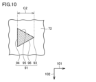
- FIG. 10 is a schematic bottom view showing the configuration of a triangular defect.
- FIG. 11 is a schematic cross-sectional view showing a step of forming a silicon carbide epitaxial layer on the second silicon carbide substrate.
- FIG. 12 is a schematic cross-sectional view showing a step of removing the fourth silicon carbide epitaxial layer by polishing.
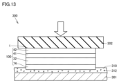
- FIG. 13 is a schematic cross-sectional view showing the configuration of a mechanical polishing apparatus.
- FIG. 14 is a flow diagram illustrating a schematic method for manufacturing a silicon carbide semiconductor device according to this embodiment.
- FIG. 15 is a schematic cross-sectional view showing a step of preparing a silicon carbide epitaxial substrate.
- FIG. 16 is a schematic cross-sectional view showing a step of forming a body region.
- FIG. 17 is a schematic cross-sectional view showing a step of forming a source region.
- FIG. 18 is a schematic cross-sectional view showing a step of forming a trench in the first main surface of the silicon carbide epitaxial layer.
- FIG. 19 is a schematic cross-sectional view showing a step of forming a gate insulating film.
- FIG. 15 is a schematic cross-sectional view showing a step of preparing a silicon carbide epitaxial substrate.
- FIG. 16 is a schematic cross-sectional view showing a step of forming a body region.
- FIG. 17 is a schematic cross-sectional view showing a step
- FIG. 20 is a schematic cross-sectional view showing a step of forming a gate electrode and an interlayer insulating film.
- FIG. 21 is a schematic cross-sectional view showing the configuration of a silicon carbide semiconductor device according to this embodiment.
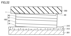
- FIG. 22 is a schematic cross-sectional view showing a state in which the protrusion is in contact with the polishing head.
- FIG. 23 is a schematic diagram showing measurement results of the LTV of each of a plurality of square regions after the step of forming a silicon carbide epitaxial layer on the second silicon carbide substrate and before the step of removing the fourth silicon carbide epitaxial layer by polishing.
- FIG. 24 is a schematic diagram showing the measurement results of the LTV of each of the plurality of square regions after the step of removing the fourth silicon carbide epitaxial layer by polishing.
- An object of the present disclosure is to provide a silicon carbide epitaxial substrate, a method for manufacturing a silicon carbide epitaxial substrate, and a method for manufacturing a silicon carbide semiconductor device, which are capable of improving the yield of silicon carbide semiconductor devices.
- the present disclosure can provide a silicon carbide epitaxial substrate capable of improving the yield of silicon carbide semiconductor devices, a method for manufacturing a silicon carbide epitaxial substrate, and a silicon carbide semiconductor device.
- a silicon carbide epitaxial substrate comprises a silicon carbide substrate and a silicon carbide epitaxial layer.
- the silicon carbide epitaxial layer is provided on the silicon carbide substrate.
- the silicon carbide epitaxial layer has a first main surface.
- the first main surface is opposite to the interface between the silicon carbide substrate and the silicon carbide epitaxial layer.
- On the first main surface there is a protrusion made of silicon carbide.
- the first main surface is made up of an outer edge, a peripheral region, and a central region.
- the peripheral region is a region within 3 mm from the outer edge.
- the central region is surrounded by the peripheral region.
- the plurality of square regions are made up of a first square region closest to the protrusion and second square regions which are a plurality of square regions other than the first square region.
- the LTV of the first square region is greater than the LTV of each of the multiple square regions that make up the second square region.
- the LTV of the first square region is 2 ⁇ m or less.
- the LTV of the first square region may be 1.5 ⁇ m or less.
- the thickness of the silicon carbide epitaxial layer may be 10 ⁇ m or more and 30 ⁇ m or less.
- the silicon carbide epitaxial substrate according to the present disclosure has a silicon carbide substrate and a silicon carbide epitaxial layer.
- the silicon carbide epitaxial layer is provided on the silicon carbide substrate.
- the silicon carbide epitaxial layer has a first main surface.
- the first main surface is opposite the interface between the silicon carbide substrate and the silicon carbide epitaxial layer.
- the silicon carbide substrate has a second main surface.
- the second main surface is opposite the interface.
- the first main surface is composed of an outer edge, a peripheral region, and a central region.
- the peripheral region is a region within 3 mm from the outer edge.
- the central region is surrounded by the outer edge region. When the central region is divided into a plurality of square regions with a side length of 10 mm, the maximum LTV value in the plurality of square regions is 2 ⁇ m or less.
- the maximum LTV value in the multiple square regions may be 1.5 ⁇ m or less.
- a method for manufacturing a silicon carbide epitaxial substrate includes the steps of preparing a first silicon carbide substrate having a first back surface and a first front surface opposite the first back surface, attaching silicon carbide particles to the first back surface, and forming a first silicon carbide epitaxial layer in contact with the first front surface and forming a second silicon carbide epitaxial layer in contact with the first back surface and the silicon carbide particles.
- steps of forming the first silicon carbide epitaxial layer and the second silicon carbide epitaxial layer triangular defects are formed in the second silicon carbide epitaxial layer starting from the silicon carbide particles.
- the method for manufacturing a silicon carbide epitaxial substrate according to the present disclosure further includes a step of measuring the thickness of the second silicon carbide epitaxial layer using triangular defects in the second silicon carbide epitaxial layer, a step of determining a polishing amount based on the measured thickness of the second silicon carbide epitaxial layer, a step of preparing a second silicon carbide substrate having a second back surface and a second front surface opposite the second back surface, a step of forming a third silicon carbide epitaxial layer in contact with the second front surface and a fourth silicon carbide epitaxial layer in contact with the second back surface, and a step of removing the fourth silicon carbide epitaxial layer by polishing based on the polishing amount.
- the thickness of the second silicon carbide epitaxial layer may be less than 1 ⁇ m.
- the amount of polishing may be 8.5 ⁇ m or more and 12.5 ⁇ m or less.
- the thickness of the second silicon carbide epitaxial layer may be 1 ⁇ m or more and 2 ⁇ m or less.
- the amount of polishing may be 11 ⁇ m or more and 16.5 ⁇ m or less.
- the method for manufacturing a silicon carbide semiconductor device includes the following steps: A silicon carbide epitaxial substrate according to any one of (1) to (5) above is prepared. An electrode is formed on the silicon carbide epitaxial layer.
- FIG. 1 is a schematic plan view showing the configuration of the silicon carbide substrate according to this embodiment.
- FIG. 2 is a schematic cross-sectional view taken along line II-II in FIG. 1.
- the silicon carbide epitaxial substrate 100 mainly has a first main surface 1, a second main surface 2, and an outer peripheral side surface 9.
- the second main surface 2 is opposite the first main surface 1.
- the outer peripheral side surface 9 is continuous with each of the first main surface 1 and the second main surface 2.
- the first main surface 1 is continuous with the outer peripheral side surface 9 at the outer edge 6.
- the first main surface 1 is composed of an outer edge 6, an outer peripheral region 11, and a central region 12.
- the outer peripheral region 11 is a region within 3 mm from the outer edge 6.
- the distance E between the outer edge 6 and the boundary between the outer peripheral region 11 and the central region 12 is 3 mm.
- the width (distance E) of the outer peripheral region 11 in the direction extending radially from the center O of the first main surface 1 (radial direction) is 3 mm.
- the central region 12 is surrounded by the peripheral region 11.
- the central region 12 is continuous with the peripheral region 11.
- the central region 12 is a region whose distance from the outer edge 6 is greater than 3 mm.
- the silicon carbide epitaxial substrate 100 is made of, for example, hexagonal silicon carbide.
- the polytype of the hexagonal silicon carbide is, for example, 4H.
- the outer peripheral side surface 9 has, for example, an orientation flat portion 7 and an arc-shaped portion 8.
- the orientation flat portion 7 when viewed along a straight line perpendicular to the first main surface 1, the orientation flat portion 7 is linear. When viewed along a straight line perpendicular to the first main surface 1, the orientation flat portion 7 may extend along the first direction 101.
- the arc-shaped portion 8 is continuous with the orientation flat portion 7. When viewed along a straight line perpendicular to the first main surface 1, the arc-shaped portion 8 is arc-shaped.
- the center O of the first main surface 1 is the center of a circle that includes an arc along the arc-shaped portion 8.
- the first principal surface 1 when viewed along a straight line perpendicular to the first principal surface 1, the first principal surface 1 extends along each of a first direction 101 and a second direction 102.
- the second direction 102 is a direction perpendicular to the first direction 101.
- the first direction 101 is, for example, the ⁇ 11-20> direction.
- the first direction 101 may be, for example, the [11-20] direction.
- the first direction 101 may be a direction obtained by projecting the ⁇ 11-20> direction onto the first principal surface 1. From another perspective, the first direction 101 may be, for example, a direction that includes a ⁇ 11-20> directional component.
- the second direction 102 is, for example, the ⁇ 1-100> direction.
- the second direction 102 may be, for example, the [1-100] direction.
- the second direction 102 may be, for example, a direction obtained by projecting the ⁇ 1-100> direction onto the first principal surface 1. From another perspective, the second direction 102 may be, for example, a direction that includes a ⁇ 1-100> directional component.
- the maximum diameter W of the first main surface 1 is not particularly limited, but is, for example, 100 mm (4 inches) or more.
- the maximum diameter W may be 125 mm (5 inches) or more, 150 mm (6 inches) or more, or 200 mm (8 inches) or more.
- the maximum diameter W may be, for example, 400 mm (16 inches) or less.
- the maximum diameter W is the longest straight distance between two different points on the outer edge 6.
- 4 inches means 100 mm or 101.6 mm (4 inches x 25.4 mm/inch). 6 inches means 150 mm or 152.4 mm (6 inches x 25.4 mm/inch). 8 inches means 200 mm or 203.2 mm (8 inches x 25.4 mm/inch). 16 inches means 400 mm or 406.4 mm (16 inches x 25.4 mm/inch).
- the third direction 103 is a direction from the second main surface 2 toward the first main surface 1.
- the third direction 103 is perpendicular to both the first direction 101 and the second direction 102.
- the cross section shown in FIG. 2 is perpendicular to the first main surface 1 and parallel to the first direction 101.
- the silicon carbide epitaxial substrate 100 has a silicon carbide substrate 30 and a silicon carbide epitaxial layer 40.
- the silicon carbide substrate 30 has a second main surface 2 and a third main surface 3.
- the second main surface 2 is the back surface of the silicon carbide epitaxial substrate 100.
- the second main surface 2 is opposite to the interface 5 between the silicon carbide substrate 30 and the silicon carbide epitaxial layer 40.
- the second main surface 2 is a polished surface.
- scratches (not shown) are formed on the second main surface 2.
- the scratches are damage formed during mechanical polishing and chemical mechanical polishing.
- the shape of the scratches is, for example, linear.
- the value obtained by dividing the length of the scratch in the longitudinal direction of the scratch by the length of the scratch in the lateral direction of the scratch may be, for example, 7 or more, 10 or more, or 15 or more.
- the second main surface 2 may not have triangular defects formed. The detailed configuration of the triangular defects will be described later.
- the third main surface 3 is opposite to the second main surface 2.
- the silicon carbide substrate 30 is in contact with the silicon carbide epitaxial layer 40.
- the silicon carbide substrate 30 contains an n-type impurity such as nitrogen.
- the conductivity type of the silicon carbide substrate 30 is, for example, n-type.
- the polytype of the silicon carbide constituting the silicon carbide substrate 30 is, for example, 4H.
- the thickness (second thickness H2) of the silicon carbide substrate 30 is, for example, 200 ⁇ m or more and 600 ⁇ m or less.
- the second thickness H2 is not particularly limited.
- the second thickness H2 may be, for example, 500 ⁇ m or less, or 350 ⁇ m or less.
- the silicon carbide epitaxial layer 40 is provided on the silicon carbide substrate 30.
- the silicon carbide epitaxial layer 40 has a first main surface 1.
- the first main surface 1 is the surface of the silicon carbide epitaxial substrate 100.
- the first main surface 1 is opposite the interface 5.
- the thickness (first thickness H1) of the silicon carbide epitaxial layer 40 is, for example, 10 ⁇ m or more and 30 ⁇ m or less.
- the first thickness H1 may be, for example, 13 ⁇ m or more, or 18 ⁇ m or more.
- the first thickness H1 may be, for example, 27 ⁇ m or less, or 22 ⁇ m or less.
- the first thickness H1 can be measured, for example, by using an FTIR (Fourier Transform InfraRed spectrometer).
- the measuring device is, for example, a Fourier transform infrared spectrophotometer (IRPrestige-21) manufactured by Shimadzu Corporation.
- the thickness of the silicon carbide layer epitaxial layer is measured by FTIR using an optical constant difference caused by a carrier concentration difference between the silicon carbide epitaxial layer 40 and the silicon carbide substrate 30.
- the measurement wave number range is, for example, from 3400 cm ⁇ 1 to 2400 cm ⁇ 1 .
- the wave number interval is, for example, about 4 cm ⁇ 1 .
- the silicon carbide epitaxial layer 40 has a buffer layer 41 and a drift layer 42.
- the drift layer 42 may be a single layer or may be two or more layers.
- the polytype of silicon carbide constituting the silicon carbide epitaxial layer 40 is, for example, 4H.
- the buffer layer 41 is provided on the silicon carbide substrate 30.
- the buffer layer 41 is in contact with the silicon carbide substrate 30.
- the buffer layer 41 contains an n-type impurity such as nitrogen.
- the conductivity type of the buffer layer 41 is, for example, n-type.
- the thickness of the buffer layer 41 in the third direction 103 is, for example, 1 ⁇ m or more.
- the drift layer 42 is provided on the buffer layer 41.
- the drift layer 42 is in contact with the buffer layer 41.
- the drift layer 42 constitutes the first main surface 1.
- the drift layer 42 contains n-type impurities such as nitrogen.
- the conductivity type of the drift layer 42 is, for example, n-type.
- the concentration of the n-type impurities in the drift layer 42 is, for example, smaller than the concentration of the n-type impurities in the buffer layer 41.
- the thickness of the drift layer 42 in the third direction 103 is, for example, 10 ⁇ m or more.
- the first main surface 1 is a surface inclined with respect to the ⁇ 0001 ⁇ surface.
- the off angle ⁇ of the first main surface 1 with respect to the ⁇ 0001 ⁇ surface is, for example, greater than 0° and equal to or less than 8°.
- the first main surface 1 may be a surface inclined by the off angle ⁇ with respect to the (0001) surface.
- the first main surface 1 may be a surface inclined by the off angle ⁇ with respect to the (000-1) surface.
- the inclination direction (off direction) of the first main surface 1 with respect to the ⁇ 0001 ⁇ surface is, for example, the ⁇ 11-20> direction.
- the off angle ⁇ is not particularly limited.
- the off angle ⁇ may be, for example, 7° or less, 6° or less, or 5° or less.
- the off angle ⁇ may be, for example, 1° or more, or 2° or more.
- FIG. 3 is an enlarged schematic cross-sectional view taken along line III-III in FIG. 1.
- the cross section shown in FIG. 3 is parallel to both the third direction 103 and the radial direction.
- a protrusion 60 is present on the first main surface 1.
- the protrusion 60 is located, for example, in the outer peripheral region 11.
- the protrusion 60 may also be located in the central region 12.
- the protrusion 60 is shown using a black circle in FIG. 1.
- the protrusion 60 is convex along the third direction 103.
- a portion of the protrusion 60 may be located radially outward from the outer peripheral side surface 9.
- the protrusion 60 may cover a portion of the outer edge 6 (see FIG. 1).
- the protrusion 60 is made of silicon carbide.
- the protrusion 60 is, for example, an epicrown or a particle.
- the shape of the protrusion 60 is, for example, circular.
- the width of the protrusion 60 in the radial direction is a first width F1.
- the protrusion 60 forms a convex surface 66.
- the convex surface 66 is convex along the third direction 103.
- the convex surface 66 forms a part of the first main surface 1.
- the convex surface 66 may be connected to the outer peripheral side surface 9.
- the first main surface 1 has a first flat surface 81 and a second flat surface 82.
- the first flat surface 81 is connected to the convex surface 66.
- the first flat surface 81 extends along both the first direction 101 and the second direction 102.
- the second flat surface 82 is continuous with the first flat surface 81.
- the second flat surface 82 is spaced apart from the convex surface 66.
- the first flat surface 81 is provided between the second flat surface 82 and the protrusion 60.
- the vertex 61 is the vertex of the protrusion 60.
- the height D1 of the protrusion 60 is, for example, 5 ⁇ m or more, and there is no particular upper limit to the height D1.
- the height D1 is the distance between the vertex 61 and the first flat surface 81 and the second flat surface 82 in the third direction 103.
- the second principal surface 2 has a concave surface 69 and a third flat surface 83.
- the concave surface 69 is opposite the protrusion 60.
- the concave surface 69 is opposite the first flat surface 81.
- the first flat surface 81 is a portion of the first principal surface 1 opposite the concave surface 69.
- An imaginary straight line 99 that passes through the vertex 61 and extends along the third direction 103 passes through the concave surface 69.
- the concave surface 69 surrounds the imaginary straight line 99.
- the concave surface 69 is inclined in the third direction 103 with respect to the radial direction.
- the concave surface 69 forms a recess 67.
- the depth D2 of the concave surface 69 in the third direction 103 may be greater than the height D1 of the protrusion 60.
- the width of the concave surface 69 in the radial direction is a second width F2.
- the second width F2 is greater than the first width F1.
- the value obtained by dividing the second width F2 by the first width F1 is, for example, 10 or more and 1000 or less.
- the second width F2 is, for example, 5 mm.
- the second width F2 may be, for example, 1 mm or more and 20 mm or less.
- the third flat surface 83 is continuous with the concave surface 69.
- the third flat surface 83 extends along each of the first direction 101 and the second direction 102.
- the third flat surface 83 is opposite the second flat surface 82.
- the second flat surface 82 is a portion of the first main surface 1 opposite the third flat surface 83.
- the concave surface 69 is inclined in the third direction 103 relative to the third flat surface 83. In a cross section perpendicular to the radial direction and parallel to the third direction 103, the concave surface 69 is concave along the third direction 103.
- LTV local thickness variation
- FIG. 4 is a schematic plan view showing the measurement area of the LTV.
- the protrusions 60 are shown as black circles.
- the central region 12 of the silicon carbide epitaxial substrate 100 is divided into a plurality of square regions 50.
- the shape of each of the plurality of square regions 50 is substantially a square.
- the length of one side of each of the plurality of square regions 50 is set to a first length C1.
- the first length C1 is 10 mm.
- the maximum diameter W (see FIG. 1) of the first main surface 1 is, for example, 150 mm.
- a 150 mm x 150 mm square circumscribing the outer peripheral side surface 9 is assumed.
- the number of square regions 50 inside the central region 12 is, for example, 141.
- the square regions that intersect with the boundary between the peripheral region 11 and the central region 12 are missing parts and are not complete square regions. Therefore, the square regions that intersect with the boundary between the peripheral region 11 and the central region 12 are not considered to be square regions 50 that make up the central region 12.
- one side of each of the multiple square regions 50 is parallel to the extension direction of the orientation flat portion 7. The LTV is measured in each of the multiple square regions 50.
- the multiple square regions 50 are composed of a first square region 51 and multiple second square regions 52.
- the first square region 51 is the square region 50 closest to the protrusion 60.
- the square region 50 closest to the vertex 61 (see FIG. 3) of the protrusion 60 when viewed along a straight line perpendicular to the first main surface 1 is determined to be the first square region 51.
- the square region 50 in which the vertex 61 is located is determined to be the first square region 51. Note that when there are multiple protrusions on the first main surface 1, the protrusion with the highest height D1 is identified as the above-mentioned protrusion 60.
- the first square region 51 may include at least a portion of the first flat surface 81 (see FIG. 3).
- the first square region 51 may include at least a portion of the convex surface 66 (see FIG. 3). In FIG. 4, the shaded region indicates the first square region 51.
- the second square regions 52 are square regions 50 other than the first square region 51.
- the number of the second square regions 52 is, for example, 140.
- the second square regions 52 are connected to the first square region 51.
- Figure 5 is a schematic diagram explaining the definition of LTV.
- LTV
- the LTV is measured, for example, by the following procedure. First, silicon carbide epitaxial substrate 100 is prepared. Either first main surface 1 or second main surface 2 is set as an adsorption surface B that is adsorbed to a flat chuck surface. The surface opposite to adsorption surface B is set as measurement surface A.
- the suction surface B is entirely attached to the chuck surface.
- an image of the measurement surface A on the opposite side of the suction surface B is optically acquired.
- the LTV is the value obtained by subtracting the height from the suction surface B to the lowest point P2 of the measurement surface A (minimum height T2) from the height from the suction surface B to the highest point P1 of the measurement surface A (maximum height T1) when the suction surface B is entirely attached to the flat chuck surface.
- the LTV is the value obtained by subtracting the shortest distance between the measurement surface A and the suction surface B from the longest distance between the measurement surface A and the suction surface B in the direction perpendicular to the suction surface B.
- the LTV is the distance between the plane (first plane L1) that passes through the highest point P1 and is parallel to the suction surface B, and the plane (second plane L2) that passes through the lowest point P2 and is parallel to the suction surface B.
- the maximum value of the LTV in the multiple square regions 50 is 2 ⁇ m or less.
- the maximum value of the LTV in the multiple square regions 50 may be, for example, 1.5 ⁇ m or less, 1.3 ⁇ m or less, or 1.1 ⁇ m or less.
- the maximum value of the LTV in the multiple square regions 50 may be, for example, 0.1 ⁇ m or more, or 0.5 ⁇ m or more.
- the LTV of the first square region 51 is 2 ⁇ m or less.
- the LTV of the first square region 51 may be, for example, 1.5 ⁇ m or less, 1.3 ⁇ m or less, or 1.1 ⁇ m or less.
- the LTV of the first square region 51 may be, for example, 0.1 ⁇ m or more, or 0.5 ⁇ m or more.
- the LTV of each of the second square regions 52 is, for example, 0.1 ⁇ m or more and 1.0 ⁇ m or less.
- the LTV of the first square region 51 is greater than the LTV of each of the second square regions 52. From another perspective, among the multiple square regions 50, the first square region 51 is the square region 50 with the largest LTV.
- Fig. 6 is a partial cross-sectional schematic diagram showing the configuration of the manufacturing apparatus for silicon carbide epitaxial substrate 100.
- the manufacturing apparatus 200 for silicon carbide epitaxial substrate 100 is, for example, a hot-wall type horizontal CVD (Chemical Vapor Deposition) apparatus.
- the manufacturing apparatus 200 for silicon carbide epitaxial substrate 100 mainly includes a reaction chamber 201, a gas supply unit 235, a control unit 245, a heating element 203, a quartz tube 204, a heat insulating material (not shown), and an induction heating coil (not shown).
- the heating element 203 has, for example, a cylindrical shape, and forms a reaction chamber 201 inside.
- the heating element 203 is made of, for example, graphite.
- the heating element 203 is provided inside a quartz tube 204.
- a heat insulating material surrounds the outer periphery of the heating element 203.
- the induction heating coil is wound, for example, along the outer periphery of the quartz tube 204.
- the induction heating coil is configured so that an alternating current can be supplied to it by an external power source (not shown). This causes the heating element 203 to be induction heated. As a result, the reaction chamber 201 is heated by the heating element 203.
- the reaction chamber 201 is a space surrounded by the inner wall surface 205 of the heating element 203.
- a susceptor 210 that holds a silicon carbide substrate 30 is provided in the reaction chamber 201.
- the susceptor 210 is made of silicon carbide.
- the silicon carbide substrate 30 is placed on the susceptor 210.
- the susceptor 210 is placed on a stage 202.
- the stage 202 is supported by a rotating shaft 209 so that it can rotate on its own axis. The rotation of the stage 202 causes the susceptor 210 to rotate.
- the manufacturing apparatus 200 for the silicon carbide epitaxial substrate 100 further has a gas inlet 207 and a gas exhaust port 208.
- the gas exhaust port 208 is connected to an exhaust pump (not shown).
- the arrows in FIG. 6 indicate the flow of gas. Gas is introduced into the reaction chamber 201 from the gas inlet 207 and exhausted from the gas exhaust port 208.
- the pressure inside the reaction chamber 201 is adjusted by balancing the amount of gas supplied and the amount of gas exhausted.
- the gas supply unit 235 is configured to be able to supply a mixed gas containing a raw material gas, a dopant gas, and a carrier gas to the reaction chamber 201.
- the gas supply unit 235 includes, for example, a first gas supply unit 231, a second gas supply unit 232, a third gas supply unit 233, and a fourth gas supply unit 234.
- the first gas supply unit 231 is configured to be able to supply a first gas containing, for example, carbon (C) atoms.
- the first gas supply unit 231 is, for example, a gas cylinder filled with the first gas.
- the first gas is, for example, propane ( C3H8 ) gas.
- the first gas may be, for example, methane ( CH4 ) gas , ethane ( C2H6 ) gas, acetylene ( C2H2 ) gas, or the like.
- the second gas supply unit 232 is configured to be able to supply a second gas including, for example, silane (SiH 4 ) gas.
- the second gas supply unit 232 is, for example, a gas cylinder filled with the second gas.
- the second gas is, for example, silane gas.
- the second gas may be a mixed gas of silane gas and a gas other than silane.
- the third gas supply unit 233 is configured to be able to supply a third gas containing, for example, nitrogen atoms.
- the third gas supply unit 233 is, for example, a gas cylinder filled with the third gas.
- the third gas is a doping gas.
- the third gas is, for example, ammonia gas. Ammonia gas is more susceptible to thermal decomposition than nitrogen gas, which has a triple bond.
- the fourth gas supply unit 234 is configured to be capable of supplying a fourth gas (carrier gas) such as hydrogen.
- the fourth gas supply unit 234 is, for example, a gas cylinder filled with hydrogen.
- the fourth gas supply unit 234 may also be, for example, a gas cylinder filled with argon.
- the control unit 245 is configured to be able to control the flow rate of the mixed gas supplied from the gas supply unit 235 to the reaction chamber 201.
- the control unit 245 may include a first gas flow rate control unit 241, a second gas flow rate control unit 242, a third gas flow rate control unit 243, and a fourth gas flow rate control unit 244.
- Each control unit may be, for example, an MFC (Mass Flow Controller).
- the control unit 245 is disposed between the gas supply unit 235 and the gas inlet 207.
- FIG. 7 is a flow diagram that outlines the method for manufacturing the silicon carbide epitaxial substrate 100 according to this embodiment. As shown in FIG.
- the method for manufacturing the silicon carbide epitaxial substrate 100 mainly includes a step of preparing a first silicon carbide substrate (S10), a step of attaching silicon carbide particles to the first back surface (S20), a step of forming a silicon carbide epitaxial layer on the first silicon carbide substrate (S30), a step of measuring the thickness of the second silicon carbide epitaxial layer (S40), a step of determining the amount of polishing (S50), a step of preparing a second silicon carbide substrate (S60), a step of forming a silicon carbide epitaxial layer on the second silicon carbide substrate (S70), and a step of removing the fourth silicon carbide epitaxial layer by polishing (S80).
- a step (S10) of preparing a first silicon carbide substrate is performed. Specifically, an ingot made of silicon carbide single crystal produced by, for example, sublimation is sliced with a wire saw to prepare a plurality of silicon carbide substrates 30. Each of the plurality of silicon carbide substrates 30 has a diameter of, for example, 100 mm or more.
- the thickness (second thickness H2) of the silicon carbide substrate 30 is, for example, 200 ⁇ m or more and 600 ⁇ m or less.
- one silicon carbide substrate 30 is prepared as a first silicon carbide substrate 31.
- the first silicon carbide substrate 31 is a dummy silicon carbide substrate 30.
- the first silicon carbide substrate 31 is a silicon carbide substrate 30 that is different from a second silicon carbide substrate 32 described later.
- FIG. 8 is a schematic cross-sectional view showing the step (S20) of adhering silicon carbide particles to the first back surface.
- the first silicon carbide substrate 31 has a first back surface 62 and a first front surface 63.
- the first surface 63 is opposite the first back surface 62.
- silicon carbide particles 90 are attached to the first back surface 62. Specifically, the silicon carbide particles 90 are attached to the second main surface 2 using, for example, tweezers. The silicon carbide particles 90 have a diameter of, for example, about 20 ⁇ m. The silicon carbide particles 90 are attached, for example, near the center of the second main surface 2.
- FIG. 9 is a cross-sectional schematic diagram showing the step (S30) of forming a silicon carbide epitaxial layer on the first silicon carbide substrate.
- the first silicon carbide substrate 31 is placed on the susceptor 210 of the manufacturing apparatus 200 (see FIG. 6) of the silicon carbide epitaxial substrate 100. Specifically, the first silicon carbide substrate 31 is placed on the susceptor 210 so that the first back surface 62 is in contact with the susceptor 210.
- the reaction chamber 201 is depressurized. Specifically, the pressure in the reaction chamber 201 is reduced from atmospheric pressure to, for example, about 1 ⁇ 10 ⁇ 6 Pa.
- the temperature rise of the first silicon carbide substrate 31 is started. During the temperature rise, hydrogen (H 2 ) gas, which is a carrier gas, is introduced into the reaction chamber 201 from the fourth gas supply unit 234.
- hydrogen (H 2 ) gas which is a carrier gas
- a buffer layer 41 is formed on the first surface 63.
- a raw material gas, a dopant gas, and a carrier gas are supplied to the reaction chamber 201. More specifically, a mixed gas containing, for example, silane, propane, ammonia, and hydrogen is introduced into the reaction chamber 201. In the reaction chamber 201, each gas is thermally decomposed.
- the flow rate of the first gas is, for example, 29 sccm.
- the flow rate of the second gas is, for example, 46 sccm.
- the flow rate of the third gas is, for example, 1.5 sccm.
- the flow rate of the fourth gas is, for example, 100 slm.
- the pressure inside the reaction chamber 201 is maintained, for example, at least 2 kPa and not more than 6 kPa.
- the growth temperature is, for example, at least 1500°C and not more than 1700°C.
- the buffer layer 41 is formed on the first surface 63 as shown in FIG. 9.
- the thickness of the buffer layer 41 is, for example, 5 ⁇ m or more.
- the drift layer 42 is formed on the buffer layer 41.
- the flow rate of the first gas is, for example, 29 sccm.
- the flow rate of the second gas is, for example, 46 sccm.
- the flow rate of the third gas is, for example, 1.5 sccm.
- the flow rate of the fourth gas is, for example, 100 slm.
- the growth temperature is, for example, 1500°C or higher and 1700°C or lower.
- the buffer layer 41 and the drift layer 42 constitute the first silicon carbide epitaxial layer 71.
- the first silicon carbide epitaxial layer 71 in contact with the first surface 63 is formed.
- the step flow growth direction (off-direction of the first main surface 1) of the first silicon carbide epitaxial layer 71 is, for example, the first direction 101.
- the configuration of the first silicon carbide epitaxial layer 71 is substantially the same as the configuration of the silicon carbide epitaxial layer 40.
- a step of forming a buffer layer 41 on the first surface 63 and a step of forming a drift layer 42 on the buffer layer 41 are performed to form a second silicon carbide epitaxial layer 72 in contact with the first back surface 62 and the silicon carbide particles 90.
- the second silicon carbide epitaxial layer 72 is formed, for example, by sublimation of a portion of a silicon carbide susceptor 210 (see FIG. 6) and deposition on the second main surface 2 of the silicon carbide substrate 30.
- the step flow growth direction of the second silicon carbide epitaxial layer 72 is, for example, the direction opposite to the first direction 101.
- the thickness of the second silicon carbide epitaxial layer 72 in the third direction 103 is a third thickness H3.
- the second silicon carbide epitaxial layer 72 has a triangular defect 91.
- the triangular defect 91 is formed starting from a silicon carbide particle 90.
- the polytype of silicon carbide constituting the triangular defect 91 is, for example, 3C.
- the triangular defect 91 has a bottom surface portion 92.
- the bottom surface portion 92 is connected to the silicon carbide particle 90.
- the bottom surface portion 92 is located on the basal plane.
- the bottom surface portion 92 is inclined relative to the first back surface 62 in the direction opposite to the third direction 103.
- the inclination angle of the first back surface 62 relative to the bottom surface portion 92 is the off angle ⁇ .
- the triangular defect 91 has a first side portion 95, a second side portion 96, and a bottom portion 94.
- the second side portion 96 is connected to the first side portion 95.
- the boundary between the second side portion 96 and the first side portion 95 is an end point 93.
- the first side portion 95 and the second side portion 96 branch into two from the end point 93.
- the bottom portion 94 is in the opposite direction to the first direction 101 with respect to the end point 93.
- the bottom portion 94 is connected to each of the first side portion 95 and the second side portion 96.
- the first side portion 95 is connected to one end (first end portion) of the bottom portion 94
- the second side portion 96 is connected to the other end (second end portion) of the base portion 94.
- the first side portion 95 When viewed along the third direction 103, the first side portion 95 is inclined with respect to each of the first direction 101 and the second direction 102.
- the first side portion 95 may be inclined from a straight line parallel to the first direction 101 toward the second direction 102.
- the second side portion 96 may be inclined from a straight line parallel to the first direction 101 in a direction opposite to the second direction 102.
- the base portion 94 When viewed along the third direction 103, the base portion 94 extends along the second direction 102.
- the width of the triangular defect 91 in the second direction 102 may increase from the end point 93 toward the base portion 94.
- the length of the triangular defect 91 in the step flow growth direction of the second silicon carbide epitaxial layer 72 (the direction opposite to the first direction 101) is defined as a second length C2.
- the second length C2 is the maximum distance between the end point 93 and the base portion 94 in the first direction 101.
- a step (S40) of measuring the thickness of the second silicon carbide epitaxial layer is performed. Specifically, first, the second length C2 is measured. In measuring the second length C2, for example, a confocal scanning device is used. As the confocal scanning device, for example, the WASAVI series "SICA 6X" manufactured by Lasertec Corporation can be used. The magnification of the objective lens is, for example, 10 times. Based on the measured second length C2, the third thickness H3 is calculated using Equation 2. As described above, the thickness (third thickness H3) of the second silicon carbide epitaxial layer 72 is measured using the triangular defect 91.
- the thickness of the fourth silicon carbide epitaxial layer 74 is thinner than the thickness of the silicon carbide epitaxial layer 40. Therefore, it is difficult to measure the thickness of the fourth silicon carbide epitaxial layer 74 using a measurement method such as FTIR (Fourier Transform InfraRed spectrometer).
- FTIR Fastier Transform InfraRed spectrometer
- the step of determining the amount of polishing (S50) is performed.
- the amount of back surface polishing H4 is determined based on the third thickness H3 measured in the step of measuring the thickness of the second silicon carbide epitaxial layer (S40).
- the amount of back surface polishing H4 is the amount by which the fourth silicon carbide epitaxial layer 74 and the second silicon carbide substrate 32 are polished in the step of removing the fourth silicon carbide epitaxial layer (S80) described below.
- the third thickness H3 may be, for example, less than 1 ⁇ m.
- the back surface grinding amount H4 is, for example, 9 ⁇ m.
- the back surface grinding amount H4 may be, for example, 8.5 ⁇ m or more and 12.5 ⁇ m or less.
- the back surface grinding amount H4 may be, for example, 9 ⁇ m or more, or 9.5 ⁇ m or more.
- the back surface grinding amount H4 may be, for example, 11 ⁇ m or less, or 10 ⁇ m or less.
- the third thickness H3 may be, for example, 1 ⁇ m or more and 2 ⁇ m or less.
- the back surface grinding amount H4 may be, for example, 13.5 ⁇ m.
- the back surface grinding amount H4 may be, for example, 11 ⁇ m or more and 16.5 ⁇ m or less.
- the back surface grinding amount H4 may be, for example, 11.5 ⁇ m or more, or 12 ⁇ m or more.
- the back surface grinding amount H4 may be, for example, 15 ⁇ m or less, or 14 ⁇ m or more.
- the step of preparing a second silicon carbide substrate (S60) is performed. Specifically, one of the multiple silicon carbide substrates 30 produced in the step of preparing a first silicon carbide substrate (S10) is prepared as the second silicon carbide substrate 32.
- the configuration of the second silicon carbide substrate 32 is substantially the same as the configuration of the first silicon carbide substrate 31.
- the second silicon carbide substrate 32 is epitaxially grown under the same growth conditions as the step of forming a silicon carbide epitaxial layer on the first silicon carbide substrate (S30), and may be a silicon carbide substrate 30 used for epitaxial growth of a different batch from the step of forming a silicon carbide epitaxial layer on the first silicon carbide substrate (S30).
- FIG. 11 is a schematic cross-sectional view showing the step (S70) of forming a silicon carbide epitaxial layer on the second silicon carbide substrate.
- the second silicon carbide substrate 32 has a second back surface 64 and a second front surface 65.
- the second surface 65 is opposite the second back surface 64.
- the second back surface 64 corresponds to the first back surface 62 (see FIG. 9).
- the second surface 65 corresponds to the first surface 63 (see FIG. 9).
- a third silicon carbide epitaxial layer 73 and a fourth silicon carbide epitaxial layer 74 are formed under substantially the same conditions as in the step (S30) of forming a silicon carbide epitaxial layer on the first silicon carbide substrate.
- a third silicon carbide epitaxial layer 73 is formed in contact with the second surface 65.
- the third silicon carbide epitaxial layer 73 has a buffer layer 41 and a drift layer 42.
- the configuration of the third silicon carbide epitaxial layer 73 is substantially the same as the configuration of each of the silicon carbide epitaxial layer 40 (see FIG. 2) and the first silicon carbide epitaxial layer 71 (see FIG. 9).
- a fourth silicon carbide epitaxial layer 74 is formed in contact with the second back surface 64.
- the fourth silicon carbide epitaxial layer 74 corresponds to the second silicon carbide epitaxial layer 72 (see FIG. 9).
- the fourth silicon carbide epitaxial layer 74 may not have a triangular defect 91.
- the thickness of the fourth silicon carbide epitaxial layer 74 in the third direction 103 may be substantially the third thickness H3.
- FIG. 12 is a schematic cross-sectional view showing the step (S80) of removing the fourth silicon carbide epitaxial layer by polishing.
- the portion indicated by the dashed line in FIG. 12 shows the state of the silicon carbide epitaxial substrate 100 before polishing.
- the portion indicated by the solid line in FIG. 12 shows the state of the silicon carbide epitaxial substrate 100 after chemical mechanical polishing. As shown in FIG. 12, mechanical polishing is performed on the fourth silicon carbide epitaxial layer 74 and the second silicon carbide substrate 32.
- FIG. 13 is a schematic cross-sectional view showing the configuration of a mechanical polishing apparatus.
- the mechanical polishing apparatus 300 has a surface plate 301 and a polishing head 302.
- the silicon carbide epitaxial substrate 100 is attached to the polishing head 302.
- the first main surface 1 of the silicon carbide epitaxial substrate 100 contacts the polishing head 302.
- the fourth silicon carbide epitaxial layer 74 faces the surface plate 301.
- the polishing head 302 is, for example, ceramic or stainless steel.
- Slurry 310 is supplied between silicon carbide epitaxial substrate 100 and platen 301.
- Slurry 310 contains, for example, abrasive grains 312.
- Abrasive grains 312 are, for example, diamond or cubic boron nitride (cBN).
- the diameter of abrasive grains 312 is, for example, 1 ⁇ m or more and 3 ⁇ m or less.
- the platen 301 rotates.
- the polishing head 302 presses the silicon carbide epitaxial substrate 100 against the platen 301. This mechanically polishes the fourth silicon carbide epitaxial layer 74 and the second silicon carbide substrate 32. As a result, the fourth silicon carbide epitaxial layer 74 is removed.
- the amount of polishing in the mechanical polishing is, for example, 7 ⁇ m or more and 16.5 ⁇ m or less.
- silicon carbide epitaxial substrate 100 is positioned so that second back surface 64 faces a polishing cloth (not shown).
- a polishing liquid (not shown) is supplied between second back surface 64 and the polishing cloth.
- the polishing liquid contains, for example, abrasive grains and an oxidizer.
- the abrasive grains are, for example, colloidal silica, fumed silica, and alumina.
- the oxidizer is, for example, hydrogen peroxide.
- the polishing cloth rotates.
- the second back surface 64 is pressed against the polishing cloth. This causes the second silicon carbide substrate 32 to be chemically mechanically polished. As a result, the portion of the second silicon carbide substrate 32 that has been damaged by the mechanical polishing is removed.
- the amount of polishing in the chemical mechanical polishing is, for example, 0.05 ⁇ m or more and 1 ⁇ m or less.
- the back surface polishing amount H4 is the sum of the amount of the removed fourth silicon carbide epitaxial layer 74 and the amount of the removed second silicon carbide substrate 32.
- the thickness of the second silicon carbide substrate 32 in the third direction 103 is the second thickness H2.
- the silicon carbide epitaxial substrate 100 may be washed using a cleaning liquid such as pure water, acid, or alkali. In this manner, the silicon carbide epitaxial substrate 100 according to this embodiment is manufactured.
- the correspondence between the silicon carbide epitaxial substrate 100 shown in FIG. 12 and the silicon carbide epitaxial substrate 100 shown in FIG. 2 will be described.
- the second silicon carbide substrate 32 corresponds to the silicon carbide substrate 30.
- the third silicon carbide epitaxial layer 73 corresponds to the silicon carbide epitaxial layer 40.
- the second back surface 64 corresponds to the second main surface 2.
- the second front surface 65 corresponds to the third main surface 3.
- the step (S30) of forming a silicon carbide epitaxial layer on the first silicon carbide substrate is followed by the step (S70) of forming a silicon carbide epitaxial layer on the second silicon carbide substrate.
- epitaxial growth is performed on a batch separate from the step (S30) of forming a silicon carbide epitaxial layer on the first silicon carbide substrate.
- the configuration of the method for manufacturing the silicon carbide epitaxial substrate 100 according to the present disclosure is not limited to the above configuration.
- the step (S30) of forming a silicon carbide epitaxial layer on the first silicon carbide substrate and the step (S70) of forming a silicon carbide epitaxial layer on the second silicon carbide substrate may be performed by epitaxial growth of the same batch.
- the step (S60) of preparing the second silicon carbide substrate may be performed simultaneously with the step (S10) of preparing the first silicon carbide substrate.
- the step (S70) of forming a silicon carbide epitaxial layer on the second silicon carbide substrate may be performed simultaneously with the step (S30) of forming a silicon carbide epitaxial layer on the first silicon carbide substrate.
- Fig. 14 is a flow diagram that outlines the method for manufacturing the silicon carbide semiconductor device 400 according to this embodiment.
- the method for manufacturing the silicon carbide semiconductor device 400 according to this embodiment mainly includes a step (S1) of preparing the silicon carbide epitaxial substrate 100 and a step (S2) of processing the silicon carbide epitaxial substrate 100.
- FIG. 15 is a schematic cross-sectional view showing the step of preparing a silicon carbide epitaxial substrate 100.
- a silicon carbide epitaxial substrate 100 according to this embodiment is prepared (see FIGS. 1 and 2).
- a step (S2) of processing the silicon carbide epitaxial substrate 100 is carried out.
- the silicon carbide epitaxial substrate 100 is processed as follows. First, ions are implanted into the silicon carbide epitaxial substrate 100.
- FIG. 16 is a schematic cross-sectional view showing the process of forming a body region.
- p-type impurities such as aluminum are ion-implanted into the second main surface 2 of the silicon carbide epitaxial layer 40.
- This forms a body region 113 having p-type conductivity.
- the portion where the body region 113 is not formed becomes the drift layer 42 and the buffer layer 41.
- the thickness of the body region 113 is, for example, 0.9 ⁇ m.
- the silicon carbide epitaxial layer 40 includes the buffer layer 41, the drift layer 42, and the body region 113.
- FIG. 17 is a schematic cross-sectional view showing the step of forming a source region.
- n-type impurities such as phosphorus are ion-implanted into the body region 113.
- This forms a source region 114 having an n-type conductivity type.
- the thickness of the source region 114 is, for example, 0.4 ⁇ m.
- the concentration of the n-type impurities in the source region 114 is higher than the concentration of the p-type impurities in the body region 113.
- a p-type impurity such as aluminum is ion-implanted into the source region 114 to form a contact region 118.
- the contact region 118 is formed so as to penetrate the source region 114 and the body region 113 and contact the drift layer 42.
- the concentration of the p-type impurity in the contact region 118 is higher than the concentration of the n-type impurity in the source region 114.
- activation annealing is performed to activate the ion-implanted impurities.
- the temperature of the activation annealing is, for example, 1500°C or higher and 1900°C or lower.
- the activation annealing time is, for example, about 30 minutes.
- the atmosphere of the activation annealing is, for example, an argon atmosphere.
- FIG. 18 is a cross-sectional schematic diagram showing a step of forming a trench in the first main surface 1 of the silicon carbide epitaxial layer 40.
- a mask 117 having an opening is formed on the first main surface 1 including the source region 114 and the contact region 118.
- the source region 114, the body region 113, and a part of the drift layer 42 are removed by etching using the mask 117.
- etching method for example, inductively coupled plasma reactive ion etching can be used. Specifically, for example, inductively coupled plasma reactive ion etching using SF 6 or a mixed gas of SF 6 and O 2 as a reactive gas is used.
- a recess is formed in the first main surface 1 by etching.
- thermal etching is performed in the recess.
- the thermal etching can be performed, for example, by heating in an atmosphere containing a reactive gas having at least one or more types of halogen atoms, with the mask 117 formed on the first main surface 1.
- the at least one or more types of halogen atoms include at least one of chlorine (Cl) atoms and fluorine (F) atoms.
- the atmosphere includes, for example, Cl 2 , BCl 3 , SF 6 or CF 4.
- a mixed gas of chlorine gas and oxygen gas is used as the reactive gas, and the thermal etching is performed at a heat treatment temperature of, for example, 700° C. or more and 1000° C. or less.
- the reactive gas may include a carrier gas in addition to the above-mentioned chlorine gas and oxygen gas.
- nitrogen gas, argon gas, or helium gas can be used as the carrier gas.
- a trench 56 is formed in the first main surface 1 by thermal etching.
- the trench 56 is defined by a sidewall surface 53 and a bottom wall surface 54.
- the sidewall surface 53 is formed by the source region 114, the body region 113, and the drift layer 42.
- the bottom wall surface 54 is formed by the drift layer 42.
- the mask 117 is removed from the first main surface 1.
- FIG. 19 is a schematic cross-sectional view showing the step of forming a gate insulating film.
- silicon carbide epitaxial substrate 100 having trenches 56 formed in first main surface 1 is heated in an oxygen-containing atmosphere at a temperature of, for example, 1300° C. or higher and 1400° C. or lower.
- This forms gate insulating film 115 that contacts drift layer 42 at bottom wall surface 54, contacts drift layer 42, body region 113, and source region 114 at side wall surface 53, and contacts source region 114 and contact region 118 at first main surface 1.
- FIG. 20 is a schematic cross-sectional view showing the step of forming a gate electrode and an interlayer insulating film.
- Gate electrode 127 is formed inside trench 56 so as to contact gate insulating film 115.
- Gate electrode 127 is disposed inside trench 56 and formed on gate insulating film 115 so as to face each of sidewall surface 53 and bottom wall surface 54 of trench 56.
- Gate electrode 127 is formed, for example, by LPCVD (Low Pressure Chemical Vapor Deposition).
- the interlayer insulating film 126 is formed.
- the interlayer insulating film 126 is formed so as to cover the gate electrode 127 and to be in contact with the gate insulating film 115.
- the interlayer insulating film 126 is formed, for example, by chemical vapor deposition.
- the interlayer insulating film 126 is composed of a material containing, for example, silicon dioxide.
- a portion of the interlayer insulating film 126 and the gate insulating film 115 are etched so as to form openings over the source region 114 and the contact region 118. As a result, the contact region 118 and the source region 114 are exposed from the gate insulating film 115.
- the source electrode 116 is formed so as to contact each of the source region 114 and the contact region 118.
- the source electrode 116 is formed, for example, by a sputtering method.
- the source electrode 116 is made of a material containing, for example, Ti (titanium), Al (aluminum), and Si (silicon).
- alloying annealing is performed. Specifically, the source electrode 116 in contact with each of the source region 114 and the contact region 118 is held at a temperature of, for example, 900°C or higher and 1100°C or lower for about 5 minutes. As a result, at least a portion of the source electrode 116 is silicided. As a result, the source electrode 116 that forms an ohmic junction with the source region 114 is formed. The source electrode 116 may also form an ohmic junction with the contact region 118.
- the source wiring 119 is formed.
- the source wiring 119 is electrically connected to the source electrode 116.
- the source wiring 119 is formed so as to cover the source electrode 116 and the interlayer insulating film 126.
- a process for forming a drain electrode is carried out.
- the silicon carbide substrate 30 is polished at the second main surface 2. This reduces the thickness of the silicon carbide substrate 30.
- the drain electrode 123 is formed. The drain electrode 123 is formed so as to be in contact with the second main surface 2. In this manner, the silicon carbide semiconductor device 400 according to this embodiment is manufactured.
- FIG. 21 is a schematic cross-sectional view showing the configuration of a silicon carbide semiconductor device 400 according to this embodiment.
- the silicon carbide semiconductor device 400 is, for example, a MOSFET (Metal Oxide Semiconductor Field Effect Transistor).
- the silicon carbide semiconductor device 400 mainly includes a silicon carbide epitaxial substrate 100, a gate electrode 127, a gate insulating film 115, a source electrode 116, a drain electrode 123, a source wiring 119, and an interlayer insulating film 126.
- the silicon carbide epitaxial substrate 100 includes a buffer layer 41, a drift layer 42, a body region 113, a source region 114, and a contact region 118.
- the silicon carbide semiconductor device 400 may be, for example, an IGBT (Insulated Gate Bipolar Transistor).
- a part of the susceptor 210 made of silicon carbide may sublimate, and a silicon carbide layer may be deposited on the back surface (second main surface 2) of the silicon carbide epitaxial substrate 100.
- a silicon carbide layer may be deposited on the back surface (second main surface 2) of the silicon carbide epitaxial substrate 100.
- roughness may be generated on the back surface, deteriorating the flatness of the silicon carbide epitaxial substrate 100.
- the yield of the silicon carbide semiconductor device 400 decreases.
- the back surface of the silicon carbide epitaxial substrate 100 may be polished after the silicon carbide epitaxial layer 40 is formed on the silicon carbide substrate 30.
- FIG. 22 is a schematic cross-sectional view showing a state in which the protrusion 60 is in contact with the polishing head 302.
- a protrusion 60 may be formed on the front surface (first main surface 1) of the silicon carbide epitaxial substrate 100.
- the protrusion 60 and the polishing head 302 come into contact. Therefore, the part of the back surface of the silicon carbide epitaxial substrate 100 opposite the protrusion 60 approaches the surface plate 301.
- the pressure that the part of the back surface opposite the protrusion 60 receives from the surface plate 301 is greater than the pressure that the other parts of the back surface receive from the surface plate 301.
- the amount of polishing of the part of the back surface opposite the protrusion 60 is greater than the amount of polishing of the other parts of the back surface.
- the amount of back surface polishing H4 is excessively large, the difference between the amount of polishing of the portion of the back surface opposite the protrusion 60 and the amount of polishing of the other portions of the back surface becomes excessively large. As a result, the flatness of the silicon carbide epitaxial substrate 100 deteriorates.
- FIG. 23 is a schematic diagram showing the measurement results of the LTV of each of the multiple square regions 50 after the step (S70) of forming a silicon carbide epitaxial layer on the second silicon carbide substrate and before the step (S80) of removing the fourth silicon carbide epitaxial layer by polishing.
- FIG. 24 is a schematic diagram showing the measurement results of the LTV of each of the multiple square regions 50 after the step (S80) of removing the fourth silicon carbide epitaxial layer by polishing.
- the back surface polishing amount H4 was set to 20 ⁇ m.
- the maximum LTV was 1.8 ⁇ m. In the silicon carbide epitaxial substrate 100 shown in FIG. 23, the maximum LTV was 5.1 ⁇ m. As shown in FIG. 23 and FIG. 24, if the back surface polishing amount H4 is excessively large, the LTV may deteriorate in a portion of the silicon carbide epitaxial substrate 100.
- the amount of back surface polishing H4 is excessively small, the layer (fourth silicon carbide epitaxial layer 74) deposited on the back surface of the silicon carbide epitaxial substrate 100 may not be sufficiently removed. In this case, the flatness of the silicon carbide epitaxial substrate 100 is not sufficiently improved. Therefore, it is desirable to set an appropriate amount of back surface polishing H4 based on the thickness of the fourth silicon carbide epitaxial layer 74.
- silicon carbide particles 90 are attached to the first back surface 62 of the first silicon carbide substrate 31.
- step (S30) of forming a silicon carbide epitaxial layer on the first silicon carbide substrate triangular defects 91 are formed in the second silicon carbide epitaxial layer 72 starting from the silicon carbide particles 90.
- the thickness H3 of the second silicon carbide epitaxial layer 72 is measured using the triangular defects 91 in the second silicon carbide epitaxial layer 72.
- the back surface polishing amount H4 is determined based on the measured thickness H3 of the second silicon carbide epitaxial layer 72.
- the fourth silicon carbide epitaxial layer 74 is removed by polishing based on the back surface polishing amount H4.
- the back surface polishing amount H4 can be determined substantially based on the thickness of the fourth silicon carbide epitaxial layer 74. This improves the flatness of the silicon carbide epitaxial substrate 100. As a result, the yield of the silicon carbide semiconductor device 400 can be improved.
- the silicon carbide epitaxial substrate 100 has a protrusion 60 on the first main surface 1.
- the multiple square regions 50 are composed of a first square region 51 closest to the protrusion 60 and a second square region 52 which is the multiple square regions 50 other than the first square region 51.
- the LTV of the first square region 51 is greater than the LTV of each of the multiple square regions 50 which compose the second square region 52.
- the LTV of the first square region 51 is 2 ⁇ m or less. In this way, even in the silicon carbide epitaxial substrate 100 having the protrusion 60, the flatness is improved. This can improve the yield of the silicon carbide semiconductor device 400.
- the second main surface 2 is a polished surface.
- the maximum value of the LTV in the multiple square regions 50 is 2 ⁇ m or less. In this way, the flatness is improved in the silicon carbide epitaxial substrate 100 whose back surface (second main surface 2) is polished. This can improve the yield of the silicon carbide semiconductor device 400.
- Silicon carbide epitaxial substrates 100 according to Samples 1 to 22 were prepared. Silicon carbide epitaxial substrates 100 according to Samples 1 to 4, 11, 21, and 22 are comparative examples. Silicon carbide epitaxial substrates 100 according to Samples 5 to 10 and 12 to 20 are examples. The diameter (maximum diameter W) of silicon carbide epitaxial substrates 100 according to Samples 1 to 22 was set to 150 mm.
- the silicon carbide epitaxial substrates 100 of samples 1 to 22 were manufactured according to the manufacturing method shown in FIG. 7.
- the third thickness H3 was measured according to the above-mentioned method.
- a WASAVI series "SICA 6X” manufactured by Lasertec Corporation was used.
- the third thickness H3 was less than 1 ⁇ m. In the silicon carbide epitaxial substrates 100 of samples 12 to 22, the third thickness H3 was 1 ⁇ m or more and 2 ⁇ m or less.
- the amount of backside polishing H4 was changed. Specifically, in the manufacture of the silicon carbide epitaxial substrates 100 relating to samples 1 to 11, the amount of backside polishing H4 was set to 6.5 ⁇ m or more and 21 ⁇ m or less. In the manufacture of the silicon carbide epitaxial substrates 100 relating to samples 12 to 22, the amount of backside polishing H4 was set to 11 ⁇ m or more and 18 ⁇ m or less.
- Table 1 shows the maximum LTV value in silicon carbide epitaxial substrates 100 in which the third thickness H3 was less than 1 ⁇ m.
- Table 1 shows the maximum LTV value in silicon carbide epitaxial substrates 100 in which the third thickness H3 was less than 1 ⁇ m.
- the maximum LTV value in silicon carbide epitaxial substrates 100 (samples 5 to 10) in which the backside grinding amount H4 was 8.5 ⁇ m or more and 12.5 ⁇ m or less was 2.0 ⁇ m or less.
- the maximum LTV value in silicon carbide epitaxial substrates 100 relating to samples 5 to 10 was 1.45 ⁇ m or less.
- the third thickness H3 was less than 1.0 ⁇ m
- the maximum LTV value in silicon carbide epitaxial substrates 100 in which the backside grinding amount H4 was 6.5 ⁇ m or more or 14.5 ⁇ m or more was greater than 2.0 ⁇ m.
- Table 2 shows the maximum LTV in silicon carbide epitaxial substrates 100 in which the third thickness H3 was 1 ⁇ m or more and 2 ⁇ m or less. As shown in Table 2, when the third thickness H3 was 1 ⁇ m or more and 2 ⁇ m or less, the maximum LTV in silicon carbide epitaxial substrates 100 (samples 12 to 20) in which the backside grinding amount H4 was 11 ⁇ m or more and 16.5 ⁇ m or less was 2.0 ⁇ m or less. Specifically, the maximum LTV in silicon carbide epitaxial substrates 100 relating to samples 12 to 20 was 1.7 ⁇ m or less.
- the maximum LTV in silicon carbide epitaxial substrates 100 (samples 12 to 16) in which the backside grinding amount H4 was 11 ⁇ m or more and 13.5 ⁇ m or less was 1.44 ⁇ m or less.
- the maximum LTV value in the silicon carbide epitaxial substrate 100 (samples 21 and 22) in which the back surface grinding amount H4 was 17.5 ⁇ m or more was 2.1 ⁇ m or more.
Landscapes
- Chemical & Material Sciences (AREA)
- Engineering & Computer Science (AREA)
- Crystallography & Structural Chemistry (AREA)
- Materials Engineering (AREA)
- Metallurgy (AREA)
- Organic Chemistry (AREA)
- Inorganic Chemistry (AREA)
- Crystals, And After-Treatments Of Crystals (AREA)
- Chemical Vapour Deposition (AREA)
Abstract
本開示に係る炭化珪素エピタキシャル基板は、炭化珪素基板と、炭化珪素エピタキシャル層とを有している。炭化珪素エピタキシャル層は、第1主面を有している。第1主面において、炭化珪素によって構成されている突起がある。第1主面は、外縁と、外周領域と、中央領域とによって構成されている。中央領域を1辺の長さが10mmである複数の正方領域に区分した場合、複数の正方領域は、突起に最も近い第1正方領域と、第1正方領域以外の複数の正方領域である第2正方領域とによって構成されている。第1正方領域のLTVは、第2正方領域を構成する複数の正方領域の各々のLTVよりも大きい。第1正方領域のLTVは、2μm以下である。
Description
本開示は、炭化珪素エピタキシャル基板、炭化珪素エピタキシャル基板の製造方法および炭化珪素半導体装置の製造方法に関する。本出願は、2023年6月29日に出願した日本特許出願である特願2023-107032号に基づく優先権を主張する。当該日本特許出願に記載された全ての記載内容は、参照によって本明細書に援用される。
特開2019-151543号公報(特許文献1)には、第1主面とそれに対向する第2主面を持つ炭化珪素基板を準備する工程と、前記第2主面の表面粗さが20nm以上となるよう研磨加工する工程と、第1主面に炭化珪素層をエピタキシャル結晶成長する工程とを有する炭化珪素エピタキシャルウェハの製造方法が開示されている。
本開示に係る炭化珪素エピタキシャル基板は、炭化珪素基板と、炭化珪素エピタキシャル層とを備えている。炭化珪素エピタキシャル層は、炭化珪素基板上に設けられている。炭化珪素エピタキシャル層は、第1主面を含んでいる。第1主面は、炭化珪素基板と炭化珪素エピタキシャル層との界面の反対にある。第1主面において、炭化珪素によって構成されている突起がある。第1主面は、外縁と、外周領域と、中央領域とによって構成されている。外周領域は、外縁から3mm以内の領域である。中央領域は、外周領域に取り囲まれている。中央領域を1辺の長さが10mmである複数の正方領域に区分した場合、複数の正方領域は、突起に最も近い第1正方領域と、第1正方領域以外の複数の正方領域である第2正方領域とによって構成されている。第1正方領域のLTVは、第2正方領域を構成する複数の正方領域の各々のLTVよりも大きい。第1正方領域のLTVは、2μm以下である。
[本開示が解決しようとする課題]
本開示の目的は、炭化珪素半導体装置の歩留まりを向上することができる炭化珪素エピタキシャル基板、炭化珪素エピタキシャル基板の製造方法および炭化珪素半導体装置の製造方法を提供することである。
本開示の目的は、炭化珪素半導体装置の歩留まりを向上することができる炭化珪素エピタキシャル基板、炭化珪素エピタキシャル基板の製造方法および炭化珪素半導体装置の製造方法を提供することである。
[本開示の効果]
本開示によれば、炭化珪素半導体装置の歩留まりを向上することができる炭化珪素エピタキシャル基板、炭化珪素エピタキシャル基板の製造方法および炭化珪素半導体装置を提供することができる。
本開示によれば、炭化珪素半導体装置の歩留まりを向上することができる炭化珪素エピタキシャル基板、炭化珪素エピタキシャル基板の製造方法および炭化珪素半導体装置を提供することができる。
[本開示の実施形態の説明]
最初に本開示の実施態様を列記して説明する。
最初に本開示の実施態様を列記して説明する。
(1)本開示に係る炭化珪素エピタキシャル基板は、炭化珪素基板と、炭化珪素エピタキシャル層とを備えている。炭化珪素エピタキシャル層は、炭化珪素基板上に設けられている。炭化珪素エピタキシャル層は、第1主面を有している。第1主面は、炭化珪素基板と炭化珪素エピタキシャル層との界面の反対にある。第1主面において、炭化珪素によって構成されている突起がある。第1主面は、外縁と、外周領域と、中央領域とによって構成されている。外周領域は、外縁から3mm以内の領域である。中央領域は、外周領域に取り囲まれている。中央領域を1辺の長さが10mmである複数の正方領域に区分した場合、複数の正方領域は、突起に最も近い第1正方領域と、第1正方領域以外の複数の正方領域である第2正方領域とによって構成されている。第1正方領域のLTVは、第2正方領域を構成する複数の正方領域の各々のLTVよりも大きい。第1正方領域のLTVは、2μm以下である。
(2)上記(1)に係る炭化珪素エピタキシャル基板によれば、第1正方領域のLTVは、1.5μm以下であってもよい。
(3)上記(1)または(2)に係る炭化珪素エピタキシャル基板によれば、炭化珪素エピタキシャル層の厚みは、10μm以上30μm以下であってもよい。
(4)本開示に係る炭化珪素エピタキシャル基板は、炭化珪素基板と、炭化珪素エピタキシャル層とを有している。炭化珪素エピタキシャル層は、炭化珪素基板上に設けられている。炭化珪素エピタキシャル層は、第1主面を有している。第1主面は、炭化珪素基板と炭化珪素エピタキシャル層との界面の反対にある。炭化珪素基板は、第2主面を有している。第2主面は、界面の反対にある。第1主面は、外縁と、外周領域と、中央領域とによって構成されている。外周領域は、外縁から3mm以内の領域である。中央領域は、外周領域に取り囲まれている。中央領域を1辺の長さが10mmである複数の正方領域に区分した場合、複数の正方領域におけるLTVの最大値は、2μm以下である。
(5)上記(4)に係る炭化珪素エピタキシャル基板によれば、複数の正方領域におけるLTVの最大値は、1.5μm以下であってもよい。
(6)本開示に係る炭化珪素エピタキシャル基板の製造方法は、第1裏面と第1裏面の反対にある第1表面とを有する第1炭化珪素基板を準備する工程と、第1裏面に炭化珪素粒子を付着させる工程と、第1表面に接している第1炭化珪素エピタキシャル層を形成し且つ第1裏面および炭化珪素粒子に接している第2炭化珪素エピタキシャル層を形成する工程とを備えている。第1炭化珪素エピタキシャル層および第2炭化珪素エピタキシャル層を形成する工程において、炭化珪素粒子を起点として第2炭化珪素エピタキシャル層に三角欠陥が形成される。本開示に係る炭化珪素エピタキシャル基板の製造方法は、第2炭化珪素エピタキシャル層にある三角欠陥を用いて第2炭化珪素エピタキシャル層の厚みを測定する工程と、測定された第2炭化珪素エピタキシャル層の厚みに基づいて研磨量を決定する工程と、第2裏面と第2裏面の反対にある第2表面とを有する第2炭化珪素基板を準備する工程と、第2表面に接している第3炭化珪素エピタキシャル層を形成し且つ第2裏面に接している第4炭化珪素エピタキシャル層を形成する工程と、研磨量に基づいて第4炭化珪素エピタキシャル層を研磨により除去する工程とをさらに備えている。
(7)上記(6)に係る炭化珪素エピタキシャル基板の製造方法によれば、第2炭化珪素エピタキシャル層の厚みは、1μm未満であってもよい。研磨量は、8.5μm以上12.5μm以下であってもよい。
(8)上記(6)に係る炭化珪素エピタキシャル基板の製造方法によれば、第2炭化珪素エピタキシャル層の厚みは、1μm以上2μm以下であってもよい。研磨量は、11μm以上16.5μm以下であってもよい。
(9)本開示に係る炭化珪素半導体装置の製造方法は、以下の工程を有している。上記(1)から(5)のいずれかに係る炭化珪素エピタキシャル基板が準備される。炭化珪素エピタキシャル層上に電極が形成される。
[本開示の実施形態の詳細]
以下、図面に基づいて、本開示の実施形態の詳細について説明する。なお、以下の図面において同一または相当する部分には同一の参照番号を付し、その説明は繰返さない。本明細書中の結晶学的記載においては、個別方位を[]、集合方位を<>、個別面を()、集合面を{}でそれぞれ示している。また、負の指数については、結晶学上、”-”(バー)を数字の上に付けることになっているが、本明細書中では、数字の前に負の符号を付けている。
以下、図面に基づいて、本開示の実施形態の詳細について説明する。なお、以下の図面において同一または相当する部分には同一の参照番号を付し、その説明は繰返さない。本明細書中の結晶学的記載においては、個別方位を[]、集合方位を<>、個別面を()、集合面を{}でそれぞれ示している。また、負の指数については、結晶学上、”-”(バー)を数字の上に付けることになっているが、本明細書中では、数字の前に負の符号を付けている。
まず、本実施形態に係る炭化珪素基板の構成について説明する。図1は、本実施形態に係る炭化珪素基板の構成を示す平面模式図である。図2は、図1のII-II線に沿った断面模式図である。
図1および図2に示されるように、本実施形態に係る炭化珪素エピタキシャル基板100は、第1主面1と、第2主面2と、外周側面9とを主に有している。第2主面2は、第1主面1の反対にある。外周側面9は、第1主面1および第2主面2の各々と連なっている。第1主面1は、外縁6において外周側面9に連なっている。
図1に示されるように、第1主面1は、外縁6と、外周領域11と、中央領域12とによって構成されている。外周領域11は、外縁6から3mm以内の領域である。第1主面1に対して垂直な直線に沿って見て、外縁6と、外周領域11と中央領域12との境界との距離Eは3mmである。別の観点から言えば、第1主面1の中心Oから放射状に延びる方向(径方向)における外周領域11の幅(距離E)は、3mmである。
中央領域12は、外周領域11に取り囲まれている。中央領域12は、外周領域11に連なっている。中央領域12は、外縁6からの距離が3mmより大きい領域である。炭化珪素エピタキシャル基板100は、たとえば六方晶炭化珪素によって構成されている。六方晶炭化珪素のポリタイプは、たとえば4Hである。
図1に示されるように、外周側面9は、たとえばオリエンテーションフラット部7と、円弧状部8とを有している。図1に示されるように、第1主面1に垂直な直線に沿って見て、オリエンテーションフラット部7は、直線状である。第1主面1に垂直な直線に沿って見て、オリエンテーションフラット部7は、第1方向101に沿って延在していてもよい。円弧状部8は、オリエンテーションフラット部7に連なっている。第1主面1に垂直な直線に沿って見て、円弧状部8は、円弧状である。第1主面1に垂直な直線に沿って見て、第1主面1の中心Oは、円弧状部8に沿った円弧を含む円の中心である。
図1に示されるように、第1主面1に垂直な直線に沿って見て、第1主面1は、第1方向101および第2方向102の各々に沿って拡がっている。第1方向101に垂直な直線に沿って見て、第2方向102は、第1方向101に対して垂直な方向である。
第1方向101は、たとえば<11-20>方向である。第1方向101は、たとえば[11-20]方向であってもよい。第1方向101は、<11-20>方向を第1主面1に射影した方向であってもよい。別の観点から言えば、第1方向101は、たとえば<11-20>方向成分を含む方向であってもよい。
第2方向102は、たとえば<1-100>方向である。第2方向102は、たとえば[1-100]方向であってもよい。第2方向102は、たとえば<1-100>方向を第1主面1に射影した方向であってもよい。別の観点から言えば、第2方向102は、たとえば<1-100>方向成分を含む方向であってもよい。
第1主面1の最大径W(直径)は、特に限定されないが、たとえば100mm(4インチ)以上である。最大径Wは、125mm(5インチ)以上であってもよいし、150mm(6インチ)以上であってもよいし、200mm(8インチ)以上であってもよい。最大径Wは、たとえば400mm(16インチ)以下であってもよい。第1主面1に垂直な直線に沿って見て、最大径Wは、外縁6上の異なる2点間の最長直線距離である。
本明細書において、4インチは、100mm又は101.6mm(4インチ×25.4mm/インチ)のことである。6インチは、150mm又は152.4mm(6インチ×25.4mm/インチ)のことである。8インチは、200mm又は203.2mm(8インチ×25.4mm/インチ)のことである。16インチは、400mm又は406.4mm(16インチ×25.4mm/インチ)のことである。
図2に示されるように、第3方向103は、第2主面2から第1主面1に向かう方向である。第3方向103は、第1方向101および第2方向102の各々に垂直である。図2に示される断面は、第1主面1に対して垂直であり、かつ第1方向101に平行である。
図2に示されるように、炭化珪素エピタキシャル基板100は、炭化珪素基板30と、炭化珪素エピタキシャル層40とを有している。炭化珪素基板30は、第2主面2と、第3主面3とを有している。
第2主面2は、炭化珪素エピタキシャル基板100の裏面である。第2主面2は、炭化珪素基板30と、炭化珪素エピタキシャル層40との界面5の反対にある。第2主面2は、研磨面である。第2主面2において、たとえばスクラッチ(図示せず)が形成されている。スクラッチは、機械研磨および化学機械研磨の際に形成される傷である。第2主面2に垂直な直線に沿って見て、スクラッチの形状は、たとえば線状である。第2主面2に垂直な直線に沿って見て、スクラッチの長手方向におけるスクラッチの長さを、スクラッチの短手方向におけるスクラッチの長さで割った値は、たとえば7以上であってもよいし、10以上であってもよいし、15以上であってもよい。第2主面2において、三角欠陥が形成されていなくてもよい。三角欠陥の詳細な構成は後述する。
第3主面3は、第2主面2の反対にある。第3主面3において、炭化珪素基板30は、炭化珪素エピタキシャル層40に接している。炭化珪素基板30は、たとえば窒素などのn型不純物を含んでいる。炭化珪素基板30の導電型は、たとえばn型である。炭化珪素基板30を構成する炭化珪素のポリタイプは、たとえば4Hである。
第3方向103において、炭化珪素基板30の厚み(第2厚みH2)は、たとえば200μm以上600μm以下である。第2厚みH2は、特に限定されない。第2厚みH2は、たとえば500μm以下であってもよいし、350μm以下であってもよい。
炭化珪素エピタキシャル層40は、炭化珪素基板30上に設けられている。炭化珪素エピタキシャル層40は、第1主面1を有している。第1主面1は、炭化珪素エピタキシャル基板100の表面である。第1主面1は、界面5の反対にある。
第3方向103において、炭化珪素エピタキシャル層40の厚み(第1厚みH1)は、たとえば10μm以上30μm以下である。第1厚みH1は、たとえば13μm以上であってもよいし、18μm以上であってもよい。第1厚みH1は、たとえば27μm以下であってもよいし、22μm以下であってもよい。
第1厚みH1は、たとえばFTIR(Fourier Transform InfraRed spectrometer)を用いて測定することができる。測定装置は、たとえば島津製作所製フーリエ変換赤外分光光度計(IRPrestige-21)である。FTIRによる炭化珪素層エピタキシャル層の厚みの測定は、炭化珪素エピタキシャル層40と炭化珪素基板30との間のキャリア濃度差により生じる光学定数差を利用して求められる。測定波数範囲は、たとえば3400cm-1から2400cm-1までの範囲である。波数間隔は、たとえば4cm-1程度である。
炭化珪素エピタキシャル層40は、バッファ層41と、ドリフト層42とを有している。ドリフト層42は、1層であってもよいし、2層以上であってもよい。炭化珪素エピタキシャル層40を構成する炭化珪素のポリタイプは、たとえば4Hである。
バッファ層41は、炭化珪素基板30上に設けられている。バッファ層41は、炭化珪素基板30に接している。バッファ層41は、たとえば窒素などのn型不純物を含んでいる。バッファ層41の導電型は、たとえばn型である。第3方向103におけるバッファ層41の厚みは、たとえば1μm以上である。
ドリフト層42は、バッファ層41上に設けられている。ドリフト層42は、バッファ層41に接している。ドリフト層42は、第1主面1を構成している。ドリフト層42は、たとえば窒素などのn型不純物を含んでいる。ドリフト層42の導電型は、たとえばn型である。ドリフト層42におけるn型不純物の濃度は、たとえばバッファ層41におけるn型不純物の濃度より小さい。第3方向103におけるドリフト層42の厚みは、たとえば10μm以上である。
図2に示されるように、第1主面1は、{0001}面に対して傾斜した面である。{0001}面に対する第1主面1のオフ角θは、たとえば0°より大きく8°以下である。具体的には、第1主面1は、(0001)面に対してオフ角θだけ傾斜した面であってもよい。第1主面1は、(000-1)面に対してオフ角θだけ傾斜した面であってもよい。{0001}面に対する第1主面1の傾斜方向(オフ方向)は、たとえば<11-20>方向である。オフ角θは、特に限定されない。オフ角θは、たとえば7°以下であってもよいし、6°以下であってもよいし、5°以下であってもよい。オフ角θは、たとえば1°以上であってもよいし、2°以上であってもよい。
図3は、図1のIII-III線に沿う拡大断面模式図である。図3に示される断面は、第3方向103および径方向の各々に平行な断面である。図1および図3に示されるように、第1主面1において、突起60がある。突起60は、たとえば外周領域11にある。突起60は、中央領域12にあってもよい。なお、説明の便宜のため、図1において、突起60は黒い丸を用いて示されている。
図3に示されるように、突起60は、第3方向103に沿って凸状である。突起60の一部は、外周側面9に対して径方向外側に位置していてもよい。突起60は、外縁6(図1参照)の一部を覆っていてもよい。突起60は、炭化珪素によって構成されている。突起60は、たとえばエピクラウンまたはパーティクルである。第1主面1から第2主面2に向かう方向に見て、突起60の形状は、たとえば円形状である。第3方向103および径方向の各々に平行な断面において、径方向における突起60の幅は、第1幅F1とされる。
突起60は、凸面66を構成している。凸面66は、第3方向103に沿って凸状である。凸面66は、第1主面1の一部を構成している。凸面66は、外周側面9に連なっていてもよい。第1主面1は、第1平坦面81と、第2平坦面82とを有している。第1平坦面81は、凸面66に連なっている。第1平坦面81は、第1方向101および第2方向102の各々に沿って拡がっている。
第2平坦面82は、第1平坦面81に連なっている。第2平坦面82は、凸面66から離間している。第1主面1から第2主面2に向かう方向に見て、第1平坦面81は、第2平坦面82と突起60との間に設けられている。
第3方向103において、第1平坦面81および第2平坦面82からの距離が最大となる凸面66上の点は、頂点61とされる。頂点61は、突起60の頂点である。突起60の高さD1は、たとえば5μm以上であり、高さD1の上限は特に規定されない。高さD1は、第3方向103における頂点61と第1平坦面81および第2平坦面82との間の距離である。
図3に示されるように、第2主面2は、凹面69と、第3平坦面83とを有している。凹面69は、突起60の反対にある。凹面69は、第1平坦面81の反対にある。別の観点から言えば、第1平坦面81は、凹面69の反対にある第1主面1の部分である。
頂点61を通り且つ第3方向103に沿って延びる仮想直線99は、凹面69を通っている。第3方向103に見て、凹面69は、仮想直線99を取り囲んでいる。第3方向103および径方向の各々に平行な断面において、凹面69は、径方向に対して第3方向103に傾斜している。凹面69は、凹部67を構成している。第3方向103における凹面69の深さD2は、突起60の高さD1よりも大きくてもよい。
図3に示されるように、第3方向103および径方向の各々に平行な断面において、径方向における凹面69の幅は、第2幅F2とされる。第2幅F2は、第1幅F1よりも大きい。第2幅F2を第1幅F1で割った値は、たとえば10以上1000以下である。第2幅F2は、たとえば5mmである。第2幅F2は、たとえば1mm以上20mm以下であってもよい。
第3平坦面83は、凹面69に連なっている。第3平坦面83は、第1方向101および第2方向102の各々に沿って拡がっている。第3平坦面83は、第2平坦面82の反対にある。別の観点から言えば、第2平坦面82は、第3平坦面83の反対にある第1主面1の部分である。凹面69は、第3平坦面83に対して第3方向103に傾斜している。径方向に垂直であり且つ第3方向103に平行な断面において、凹面69は、第3方向103に沿って凹状である。
<炭化珪素エピタキシャル基板のLTV>
次に、炭化珪素エピタキシャル基板100のLTV(Local Thickness Variation)の測定方法について説明する。LTVは、たとえばCorning Tropel社製の「Tropel FlatMaster(商標)」を用いて測定可能である。
次に、炭化珪素エピタキシャル基板100のLTV(Local Thickness Variation)の測定方法について説明する。LTVは、たとえばCorning Tropel社製の「Tropel FlatMaster(商標)」を用いて測定可能である。
図4は、LTVの測定領域を示す平面模式図である。説明の便宜のため、図4において、突起60が黒い丸で示されている。図4に示されるように、炭化珪素エピタキシャル基板100の中央領域12が、複数の正方領域50に区分される。第1主面1に垂直な直線に沿って見て、複数の正方領域50の各々の形状は、実質的に正方形である。複数の正方領域50の各々の1辺の長さは、第1長さC1とされる。第1長さC1は10mmである。第1主面1の最大径W(図1参照)は、たとえば150mmである。まず、外周側面9に外接する150mm×150mmの正方形が想定される。150mm×150mmの正方形は、10mm×10mmの正方領域(15×15=225個)に区分される。
第1主面1に垂直な直線に沿って見て、中央領域12の内部にある正方領域50の数は、たとえば141個である。第1主面1に垂直な直線に沿って見て、外周領域11と中央領域12との境界と交差する正方領域は、一部が欠けており完全な正方領域とはならない。そのため、外周領域11と中央領域12との境界と交差する正方領域は、中央領域12を構成する正方領域50とはみなされない。なお、第1主面1に垂直な直線に沿って見て、複数の正方領域50の各々の一辺は、オリエンテーションフラット部7の延在方向に平行である。複数の正方領域50の各々において、LTVが測定される。
複数の正方領域50は、第1正方領域51と、複数の第2正方領域52とによって構成されている。第1正方領域51は、突起60に最も近い正方領域50である。具体的には、第1主面1に垂直な直線に沿って見て、突起60の頂点61(図3参照)に最も近い正方領域50が、第1正方領域51とされる。第1主面1に垂直な直線に沿って見て、頂点61が複数の正方領域50の内部にある場合、頂点61が位置している正方領域50が第1正方領域51とされる。なお、第1主面1において複数の突起がある場合、高さD1が最も高い突起が上述の突起60として特定される。
第1正方領域51は、第1平坦面81(図3参照)の少なくとも一部を含んでいてもよい。第1正方領域51は、凸面66(図3参照)の少なくとも一部を含んでいてもよい。図4において、斜線が付されている領域は、第1正方領域51を示している。
複数の第2正方領域52は、第1正方領域51以外の複数の正方領域50である。複数の第2正方領域52の数は、たとえば140個である。複数の第2正方領域52は、第1正方領域51に連なっている。
次に、LTVの定義について説明する。図5は、LTVの定義を説明する模式図である。
LTV=|T1-T2| ・・・(数式1)
LTVは、たとえば以下の手順で測定される。まず、炭化珪素エピタキシャル基板100が準備される。第1主面1または第2主面2のいずれか一方は、平坦なチャック面に吸着される吸着面Bとされる。吸着面Bの反対側の面は、測定面Aとされる。
LTVは、たとえば以下の手順で測定される。まず、炭化珪素エピタキシャル基板100が準備される。第1主面1または第2主面2のいずれか一方は、平坦なチャック面に吸着される吸着面Bとされる。吸着面Bの反対側の面は、測定面Aとされる。
吸着面Bが、チャック面に全面吸着される。次に、吸着面Bの反対側にある測定面Aの画像が光学的に取得される。図5および数式1に示されるように、LTVとは、平坦なチャック面に吸着面Bを全面吸着させた状態で、吸着面Bから測定面Aの最高点P1までの高さ(最高高さT1)から、吸着面Bから測定面Aの最低点P2までの高さ(最低高さT2)を差し引いた値である。言い換えれば、LTVは、吸着面Bに対して垂直な方向において、測定面Aと吸着面Bとの最長距離から、測定面Aと吸着面Bとの最短距離を差し引いた値である。つまり、LTVは、最高点P1を通りかつ吸着面Bと平行な平面(第1平面L1)と、最低点P2を通りかつ吸着面Bと平行な平面(第2平面L2)との間の距離である。
複数の正方領域50におけるLTVの最大値は、2μm以下である。複数の正方領域50におけるLTVの最大値は、たとえば1.5μm以下であってもよいし、1.3μm以下であってもよいし、1.1μm以下であってもよい。複数の正方領域50におけるLTVの最大値は、たとえば0.1μm以上であってもよいし、0.5μm以上であってもよい。
第1正方領域51のLTVは、2μm以下である。第1正方領域51のLTVは、たとえば1.5μm以下であってもよいし、1.3μm以下であってもよいし、1.1μm以下であってもよい。第1正方領域51のLTVは、たとえば0.1μm以上であってもよいし、0.5μm以上であってもよい。
第2正方領域52の各々のLTVは、たとえば0.1μm以上1.0μm以下である。第1正方領域51のLTVは、複数の第2正方領域52の各々のLTVよりも大きい。別の観点から言えば、複数の正方領域50において、第1正方領域51は最もLTVが大きい正方領域50である。
(炭化珪素エピタキシャル基板の製造装置)
次に、炭化珪素エピタキシャル基板100の製造装置の構成について説明する。図6は、炭化珪素エピタキシャル基板100の製造装置の構成を示す一部断面模式図である。炭化珪素エピタキシャル基板100の製造装置200は、たとえばホットウォール方式の横型CVD(Chemical Vapor Deposition)装置である。図6に示されるように、炭化珪素エピタキシャル基板100の製造装置200は、反応室201と、ガス供給部235と、制御部245と、発熱体203と、石英管204と、断熱材(図示せず)と、誘導加熱コイル(図示せず)とを主に有している。
次に、炭化珪素エピタキシャル基板100の製造装置の構成について説明する。図6は、炭化珪素エピタキシャル基板100の製造装置の構成を示す一部断面模式図である。炭化珪素エピタキシャル基板100の製造装置200は、たとえばホットウォール方式の横型CVD(Chemical Vapor Deposition)装置である。図6に示されるように、炭化珪素エピタキシャル基板100の製造装置200は、反応室201と、ガス供給部235と、制御部245と、発熱体203と、石英管204と、断熱材(図示せず)と、誘導加熱コイル(図示せず)とを主に有している。
発熱体203は、たとえば筒状の形状を有しており、内部に反応室201を形成している。発熱体203は、たとえば黒鉛製である。発熱体203は、石英管204の内部に設けられている。断熱材は、発熱体203の外周を取り囲んでいる。誘導加熱コイルは、たとえば石英管204の外周面に沿って巻回されている。誘導加熱コイルは、外部電源(図示せず)により、交流電流が供給可能に構成されている。これにより、発熱体203が誘導加熱される。結果として、反応室201が発熱体203により加熱される。
反応室201は、発熱体203の内壁面205に取り囲まれて形成された空間である。反応室201には、炭化珪素基板30を保持するサセプタ210が設けられる。サセプタ210は、炭化珪素によって構成されている。炭化珪素基板30は、サセプタ210に載置される。サセプタ210は、ステージ202上に配置される。ステージ202は、回転軸209によって自転可能に支持されている。ステージ202が回転することで、サセプタ210が回転する。
炭化珪素エピタキシャル基板100の製造装置200は、ガス導入口207およびガス排気口208をさらに有している。ガス排気口208は、図示しない排気ポンプに接続されている。図6中の矢印は、ガスの流れを示している。ガスは、ガス導入口207から反応室201に導入され、ガス排気口208から排気される。反応室201内の圧力は、ガスの供給量と、ガスの排気量とのバランスによって調整される。
ガス供給部235は、反応室201に、原料ガスとドーパントガスとキャリアガスとを含む混合ガスを供給可能に構成されている。具体的には、ガス供給部235は、たとえば第1ガス供給部231と、第2ガス供給部232と、第3ガス供給部233と、第4ガス供給部234とを含んでいる。
第1ガス供給部231は、たとえば炭素(C)原子を含む第1ガスを供給可能に構成されている。第1ガス供給部231は、たとえば第1ガスが充填されたガスボンベである。第1ガスは、たとえばプロパン(C3H8)ガスである。第1ガスは、たとえばメタン(CH4)ガス、エタン(C2H6)ガス、アセチレン(C2H2)ガス等であってもよい。
第2ガス供給部232は、たとえばシラン(SiH4)ガスを含む第2ガスを供給可能に構成されている。第2ガス供給部232は、たとえば第2ガスが充填されたガスボンベである。第2ガスは、たとえばシランガスである。第2ガスは、シランガスと、シラン以外の他のガスとの混合ガスでもよい。
第3ガス供給部233は、たとえば窒素原子を含む第3ガスを供給可能に構成されている。第3ガス供給部233は、たとえば第3ガスが充填されたガスボンベである。第3ガスは、ドーピングガスである。第3ガスは、たとえばアンモニアガスである。アンモニアガスは、三重結合を有する窒素ガスに比べて熱分解されやすい。
第4ガス供給部234は、たとえば水素などの第4ガス(キャリアガス)を供給可能に構成されている。第4ガス供給部234は、たとえば水素が充填されたガスボンベである。第4ガス供給部234は、たとえばアルゴンが充填されたガスボンベであってもよい。
制御部245は、ガス供給部235から反応室201に供給される混合ガスの流量を制御可能に構成されている。具体的には、制御部245は、第1ガス流量制御部241と、第2ガス流量制御部242と、第3ガス流量制御部243と、第4ガス流量制御部244とを含んでいてもよい。各制御部は、たとえばMFC(Mass Flow Controller)であってもよい。制御部245は、ガス供給部235とガス導入口207との間に配置されている。
<炭化珪素エピタキシャル基板の製造方法>
次に、本実施形態に係る炭化珪素エピタキシャル基板100の製造方法について説明する。図7は、本実施形態に係る炭化珪素エピタキシャル基板100の製造方法を概略的に示すフロー図である。図7に示されるように、本実施形態に係る炭化珪素エピタキシャル基板100の製造方法は、第1炭化珪素基板を準備する工程(S10)と、第1裏面に炭化珪素粒子を付着させる工程(S20)と、第1炭化珪素基板に炭化珪素エピタキシャル層を形成する工程(S30)と、第2炭化珪素エピタキシャル層の厚みを測定する工程(S40)と、研磨量を決定する工程(S50)と、第2炭化珪素基板を準備する工程(S60)と、第2炭化珪素基板に炭化珪素エピタキシャル層を形成する工程(S70)と、第4炭化珪素エピタキシャル層を研磨により除去する工程(S80)とを主に有している。
次に、本実施形態に係る炭化珪素エピタキシャル基板100の製造方法について説明する。図7は、本実施形態に係る炭化珪素エピタキシャル基板100の製造方法を概略的に示すフロー図である。図7に示されるように、本実施形態に係る炭化珪素エピタキシャル基板100の製造方法は、第1炭化珪素基板を準備する工程(S10)と、第1裏面に炭化珪素粒子を付着させる工程(S20)と、第1炭化珪素基板に炭化珪素エピタキシャル層を形成する工程(S30)と、第2炭化珪素エピタキシャル層の厚みを測定する工程(S40)と、研磨量を決定する工程(S50)と、第2炭化珪素基板を準備する工程(S60)と、第2炭化珪素基板に炭化珪素エピタキシャル層を形成する工程(S70)と、第4炭化珪素エピタキシャル層を研磨により除去する工程(S80)とを主に有している。
まず、第1炭化珪素基板を準備する工程(S10)が実施される。具体的には、たとえば昇華法により製造された炭化珪素単結晶からなるインゴットがワイヤーソーによりスライスされることにより、複数の炭化珪素基板30が準備される。複数の炭化珪素基板30の各々の直径は、たとえば100mm以上である。炭化珪素基板30の厚み(第2厚みH2)は、たとえば200μm以上600μm以下である。
複数の炭化珪素基板30の各々の内、1つの炭化珪素基板30が第1炭化珪素基板31として準備される。第1炭化珪素基板31は、ダミーの炭化珪素基板30である。第1炭化珪素基板31は、後述する第2炭化珪素基板32とは異なる炭化珪素基板30である。
次に、第1裏面に炭化珪素粒子を付着させる工程(S20)が実施される。図8は、第1裏面に炭化珪素粒子を付着させる工程(S20)を示す断面模式図である。図8に示されるように、第1炭化珪素基板31は、第1裏面62と、第1表面63とを有している。第1表面63は、第1裏面62の反対にある。
図8に示されるように、第1裏面62に炭化珪素粒子90が付けられる。具体的には、たとえばピンセットを用いて第2主面2に炭化珪素粒子90が付けられる。炭化珪素粒子90の直径は、たとえば20μm程度である。炭化珪素粒子90は、たとえば第2主面2の中央付近に付着する。
次に、第1炭化珪素基板に炭化珪素エピタキシャル層を形成する工程(S30)が実施される。図9は、第1炭化珪素基板に炭化珪素エピタキシャル層を形成する工程(S30)を示す断面模式図である。第1炭化珪素基板31が炭化珪素エピタキシャル基板100の製造装置200(図6参照)のサセプタ210に配置される。具体的には、第1裏面62がサセプタ210に接するように、第1炭化珪素基板31がサセプタ210に配置される。次に、反応室201が減圧される。具体的には、反応室201の圧力が大気圧からたとえば1×10⁻⁶Pa程度に低減される。次に、第1炭化珪素基板31の昇温が開始される。昇温の途中において、第4ガス供給部234からキャリアガスである水素(H2)ガスが反応室201に導入される。
第1表面63上にバッファ層41が形成される。具体的には、原料ガス、ドーパントガスおよびキャリアガスが、反応室201に供給される。より具体的には、たとえばシランとプロパンとアンモニアと水素とを含む混合ガスが、反応室201に導入される。反応室201において、それぞれのガスが熱分解される。
第1表面63上にバッファ層41を形成する工程において、第1ガス(プロパンガス)の流量は、たとえば29sccmである。第2ガス(シランガス)の流量は、たとえば46sccmである。第3ガス(アンモニアガス)の流量は、たとえば1.5sccmである。第4ガス(水素ガス)の流量は、たとえば100slmである。反応室201内の圧力は、たとえば2kPa以上6kPa以下に維持される。成長温度は、たとえば1500℃以上1700℃以下である。以上により、図9に示されるように第1表面63上にバッファ層41が形成される。第3方向103において、バッファ層41の厚みは、たとえば5μm以上である。
次に、バッファ層41上にドリフト層42が形成される。バッファ層41上にドリフト層42を形成する工程において、第1ガス(プロパンガス)の流量は、たとえば29sccmである。第2ガス(シランガス)の流量は、たとえば46sccmである。第3ガス(アンモニアガス)の流量は、たとえば1.5sccmである。第4ガス(水素ガス)の流量は、たとえば100slmである。成長温度は、たとえば1500℃以上1700℃以下である。
バッファ層41とドリフト層42とは、第1炭化珪素エピタキシャル層71を構成している。以上により、第1表面63に接している第1炭化珪素エピタキシャル層71が形成される。第1炭化珪素エピタキシャル層71のステップフロー成長方向(第1主面1のオフ方向)は、たとえば第1方向101である。第1炭化珪素エピタキシャル層71の構成は、炭化珪素エピタキシャル層40の構成と実質的に同じである。
図9に示されるように、第1表面63上にバッファ層41を形成する工程およびバッファ層41上にドリフト層42を形成する工程が実施されることによって、第1裏面62および炭化珪素粒子90に接している第2炭化珪素エピタキシャル層72が形成される。第2炭化珪素エピタキシャル層72は、たとえば炭化珪素製のサセプタ210(図6参照)の一部が昇華して、炭化珪素基板30の第2主面2に堆積することにより形成される。第2炭化珪素エピタキシャル層72のステップフロー成長方向は、たとえば第1方向101と反対の方向である。第3方向103における第2炭化珪素エピタキシャル層72の厚みは、第3厚みH3とされる。
第2炭化珪素エピタキシャル層72において、三角欠陥91がある。第2炭化珪素エピタキシャル層72が形成される過程において、三角欠陥91は、炭化珪素粒子90を起点として形成される。三角欠陥91を構成する炭化珪素のポリタイプは、たとえば3Cである。三角欠陥91は、底面部92を有している。底面部92は、炭化珪素粒子90に連なっている。底面部92は、基底面に位置している。底面部92は、第1裏面62に対して、第3方向103と反対の方向に傾斜している。底面部92に対する第1裏面62の傾斜角は、オフ角θである。
図10は、三角欠陥91の構成を示す底面模式図である。図10に示されるように、三角欠陥91は、第1辺部95と、第2辺部96と、底辺部94とを有している。第2辺部96は、第1辺部95に連なっている。第2辺部96と第1辺部95との境界は、端点93である。別の観点から言えば、第1辺部95および第2辺部96は、端点93から2つに分岐している。底辺部94は、端点93に対して、第1方向101と反対の方向にある。底辺部94は、第1辺部95および第2辺部96の各々に連なっている。第1辺部95は、底辺部94の一端(第1端部)に連なっており、かつ、第2辺部96は、底辺部94の他端(第2端部)に連なっている。
第3方向103に沿って見て、第1辺部95は、第1方向101および第2方向102の各々に対して傾斜している。第1辺部95は、第1方向101に平行な直線から第2方向102に傾斜していてもよい。第2辺部96は、第1方向101に平行な直線から第2方向102と反対の方向に傾斜していてもよい。第3方向103に沿って見て、底辺部94は、第2方向102に沿って延びている。第3方向103に沿って見て、第2方向102における三角欠陥91の幅は、端点93から底辺部94に向かうにつれて大きくなっていてもよい。
第3方向103に沿って見て、第2炭化珪素エピタキシャル層72のステップフロー成長方向(第1方向101と反対の方向)における三角欠陥91の長さは、第2長さC2とされる。第2長さC2は、第1方向101における端点93と底辺部94との間の最大距離である。
H3=C2×tanθ ・・・(数式2)
次に、第2炭化珪素エピタキシャル層の厚みを測定する工程(S40)が実施される。具体的には、まず、第2長さC2が測定される。第2長さC2の測定において、たとえば共焦点走査装置が用いられる。共焦点走査装置としては、たとえばレーザーテック株式会社製のWASAVIシリーズ「SICA 6X」を使用することができる。対物レンズの倍率は、たとえば10倍とされる。測定された第2長さC2に基づいて、数式2を用いて第3厚みH3が算出される。以上により、三角欠陥91を用いて第2炭化珪素エピタキシャル層72の厚み(第3厚みH3)が測定される。
次に、第2炭化珪素エピタキシャル層の厚みを測定する工程(S40)が実施される。具体的には、まず、第2長さC2が測定される。第2長さC2の測定において、たとえば共焦点走査装置が用いられる。共焦点走査装置としては、たとえばレーザーテック株式会社製のWASAVIシリーズ「SICA 6X」を使用することができる。対物レンズの倍率は、たとえば10倍とされる。測定された第2長さC2に基づいて、数式2を用いて第3厚みH3が算出される。以上により、三角欠陥91を用いて第2炭化珪素エピタキシャル層72の厚み(第3厚みH3)が測定される。
なお、第4炭化珪素エピタキシャル層74の厚みは、炭化珪素エピタキシャル層40の厚みと比較して薄い。従って、FTIR(Fourier Transform InfraRed spectrometer)等の測定方法を用いて、第4炭化珪素エピタキシャル層74の厚みを測定することは困難である。
次に、研磨量を決定する工程(S50)が実施される。第2炭化珪素エピタキシャル層の厚みを測定する工程(S40)において測定された第3厚みH3に基づいて裏面研磨量H4が決定される。裏面研磨量H4は、後述する第4炭化珪素エピタキシャル層を除去する工程(S80)において、第4炭化珪素エピタキシャル層74および第2炭化珪素基板32が研磨される量である。
第3厚みH3は、たとえば1μm未満であってもよい。第3厚みH3が1μm未満である場合、裏面研磨量H4は、たとえば9μmとされる。第3厚みH3が1μm未満である場合、裏面研磨量H4は、たとえば8.5μm以上12.5μm以下とされてもよい。第3厚みH3が1μm未満である場合、裏面研磨量H4は、たとえば9μm以上とされてもよいし、9.5μm以上とされてもよい。第3厚みH3が1μm未満である場合、裏面研磨量H4は、たとえば11μm以下であってもよいし、10μm以下であってもよい。
第3厚みH3は、たとえば1μm以上2μm以下であってもよい。第3厚みH3が1μm以上2μm以下である場合、裏面研磨量H4は、たとえば13.5μmとされる。第3厚みH3が1μm以上2μm以下である場合、裏面研磨量H4は、たとえば11μm以上16.5μm以下とされてもよい。第3厚みH3が1μm以上2μm以下である場合、裏面研磨量H4は、たとえば11.5μm以上であってもよいし、12μm以上であってもよい。第3厚みH3が1μm以上2μm以下である場合、裏面研磨量H4は、たとえば15μm以下であってもよいし、14μm以上であってもよい。
次に、第2炭化珪素基板を準備する工程(S60)が実施される。具体的には、第1炭化珪素基板を準備する工程(S10)において作製された複数の炭化珪素基板30の内、1つの炭化珪素基板30が第2炭化珪素基板32として準備される。第2炭化珪素基板32の構成は、第1炭化珪素基板31の構成と実質的に同じである。第2炭化珪素基板32は、第1炭化珪素基板に炭化珪素エピタキシャル層を形成する工程(S30)と同様の成長条件で作成するためのエピタキシャル成長であって、且つ、第1炭化珪素基板に炭化珪素エピタキシャル層を形成する工程(S30)と別バッチのエピタキシャル成長に用いられる炭化珪素基板30であってもよい。
次に、第2炭化珪素基板に炭化珪素エピタキシャル層を形成する工程(S70)が実施される。図11は、第2炭化珪素基板に炭化珪素エピタキシャル層を形成する工程(S70)を示す断面模式図である。図11に示されるように、第2炭化珪素基板32は、第2裏面64と、第2表面65とを有している。第2表面65は、第2裏面64の反対にある。第2裏面64は、第1裏面62(図9参照)に対応している。第2表面65は、第1表面63(図9参照)に対応している。
第2炭化珪素基板に炭化珪素エピタキシャル層を形成する工程(S70)において、第1炭化珪素基板に炭化珪素エピタキシャル層を形成する工程(S30)と実質的に同じ条件によって、第3炭化珪素エピタキシャル層73と、第4炭化珪素エピタキシャル層74とが形成される。
図11に示されるように、第2表面65に接している第3炭化珪素エピタキシャル層73が形成される。第3炭化珪素エピタキシャル層73は、バッファ層41と、ドリフト層42とを有している。第3炭化珪素エピタキシャル層73の構成は、炭化珪素エピタキシャル層40(図2参照)および第1炭化珪素エピタキシャル層71(図9参照)の各々の構成と実質的に同じである。
図11に示されるように、第2裏面64に接している第4炭化珪素エピタキシャル層74が形成される。第4炭化珪素エピタキシャル層74は、第2炭化珪素エピタキシャル層72(図9参照)に対応している。第4炭化珪素エピタキシャル層74において、三角欠陥91はなくてもよい。第3方向103における第4炭化珪素エピタキシャル層74の厚みは、実質的に第3厚みH3であってもよい。
次に、第4炭化珪素エピタキシャル層を研磨により除去する工程(S80)が実施される。図12は、第4炭化珪素エピタキシャル層を研磨により除去する工程(S80)を示す断面模式図である。図12において破線で示される部分は、研磨前における炭化珪素エピタキシャル基板100の状態を示している。図12において実線で示される部分は、化学機械研磨後における炭化珪素エピタキシャル基板100の状態を示している。図12に示されるように、第4炭化珪素エピタキシャル層74および第2炭化珪素基板32に対して機械研磨が行われる。
図13は、機械研磨装置の構成を示す断面模式図である。図13に示されるように、機械研磨装置300は、定盤301と、研磨ヘッド302とを有している。図13に示されるように、炭化珪素エピタキシャル基板100は、研磨ヘッド302に取り付けられる。第1主面1において、炭化珪素エピタキシャル基板100は、研磨ヘッド302に接する。第4炭化珪素エピタキシャル層74は、定盤301に対向する。研磨ヘッド302は、たとえばセラミックスまたはステンレスである。
炭化珪素エピタキシャル基板100と、定盤301との間にスラリー310が供給される。スラリー310は、たとえば砥粒312を含んでいる。砥粒312は、たとえばダイヤモンドまたは立方晶窒化ホウ素(cBN)である。砥粒312の径は、たとえば1μm以上3μm以下である。
定盤301が回転する。研磨ヘッド302によって、炭化珪素エピタキシャル基板100が定盤301に押し付けられる。これによって、第4炭化珪素エピタキシャル層74および第2炭化珪素基板32が機械研磨される。以上によって、第4炭化珪素エピタキシャル層74が除去される。機械研磨における研磨量は、たとえば7μm以上16.5μm以下である。
次に、化学機械研磨が実施される。具体的には、第2裏面64が研磨布(図示せず)に対向するように、炭化珪素エピタキシャル基板100が配置される。第2裏面64と研磨布との間に研磨液(図示せず)が供給される。研磨液は、たとえば砥粒と酸化剤とを含んでいる。砥粒は、たとえばコロイダルシリカ、フュームドシリカおよびアルミナなどである。酸化剤は、たとえば過酸化水素水などである。
研磨布は回転する。第2裏面64が研磨布に押し付けられる。これによって、第2炭化珪素基板32が化学機械研磨される。以上によって、機械研磨によってダメージを受けた第2炭化珪素基板32の部分が除去される。化学機械研磨における研磨量は、たとえば0.05μm以上1μm以下である。
図12に示されるように、機械研磨における研磨量と、化学機械研磨における研磨量との合計は、裏面研磨量H4である。別の観点から言えば、裏面研磨量H4は、除去された第4炭化珪素エピタキシャル層74の量と除去された第2炭化珪素基板32の量との合計である。第4炭化珪素エピタキシャル層を研磨により除去する工程(S80)の後において、第3方向103における第2炭化珪素基板32の厚みは、第2厚みH2である。第4炭化珪素エピタキシャル層を研磨により除去する工程(S80)の後において、炭化珪素エピタキシャル基板100は、純水、酸またはアルカリなどの洗浄液を用いて洗浄されてもよい。以上により、本実施形態に係る炭化珪素エピタキシャル基板100が製造される。
図12に示される炭化珪素エピタキシャル基板100と、図2に示される炭化珪素エピタキシャル基板100との対応関係について説明する。第2炭化珪素基板32は、炭化珪素基板30に対応している。第3炭化珪素エピタキシャル層73は、炭化珪素エピタキシャル層40に対応している。第2裏面64は、第2主面2に対応している。第2表面65は、第3主面3に対応している。
なお、上記においては、第1炭化珪素基板に炭化珪素エピタキシャル層を形成する工程(S30)の後に、第2炭化珪素基板に炭化珪素エピタキシャル層を形成する工程(S70)が行われる。別の観点から言えば、第2炭化珪素基板に炭化珪素エピタキシャル層を形成する工程(S70)においては、第1炭化珪素基板に炭化珪素エピタキシャル層を形成する工程(S30)とは別バッチのエピタキシャル成長が実施される。しかしながら、本開示に係る炭化珪素エピタキシャル基板100の製造方法の構成は、上記の構成に限定されない。
具体的には、第1炭化珪素基板に炭化珪素エピタキシャル層を形成する工程(S30)と第2炭化珪素基板に炭化珪素エピタキシャル層を形成する工程(S70)は、同じバッチのエピタキシャル成長によって実施されてもよい。別の観点から言えば、第2炭化珪素基板を準備する工程(S60)は、第1炭化珪素基板を準備する工程(S10)と同時に行われてもよい。第2炭化珪素基板に炭化珪素エピタキシャル層を形成する工程(S70)は、第1炭化珪素基板に炭化珪素エピタキシャル層を形成する工程(S30)と同時に行われてもよい。
(炭化珪素半導体装置の製造方法)
次に、本実施形態に係る炭化珪素半導体装置400の製造方法について説明する。図14は、本実施形態に係る炭化珪素半導体装置400の製造方法を概略的に示すフロー図である。図14に示されるように、本実施形態に係る炭化珪素半導体装置400の製造方法は、炭化珪素エピタキシャル基板100を準備する工程(S1)と、炭化珪素エピタキシャル基板100を加工する工程(S2)とを主に有している。
次に、本実施形態に係る炭化珪素半導体装置400の製造方法について説明する。図14は、本実施形態に係る炭化珪素半導体装置400の製造方法を概略的に示すフロー図である。図14に示されるように、本実施形態に係る炭化珪素半導体装置400の製造方法は、炭化珪素エピタキシャル基板100を準備する工程(S1)と、炭化珪素エピタキシャル基板100を加工する工程(S2)とを主に有している。
まず、炭化珪素エピタキシャル基板100を準備する工程(S1)が実施される。図15は、炭化珪素エピタキシャル基板100を準備する工程を示す断面模式図である。図15に示されるように、炭化珪素エピタキシャル基板100を準備する工程(S1)においては、本実施形態に係る炭化珪素エピタキシャル基板100が準備される(図1および図2参照)。
次に、炭化珪素エピタキシャル基板100を加工する工程(S2)が実施される。具体的には、炭化珪素エピタキシャル基板100に対して以下のような加工が行われる。まず、炭化珪素エピタキシャル基板100に対してイオン注入が行われる。
図16は、ボディ領域を形成する工程を示す断面模式図である。ボディ領域を形成する工程において、炭化珪素エピタキシャル層40の第2主面2に対して、たとえばアルミニウムなどのp型不純物がイオン注入される。これにより、p型の導電型を有するボディ領域113が形成される。ボディ領域113が形成されなかった部分は、ドリフト層42およびバッファ層41となる。ボディ領域113の厚みは、たとえば0.9μmである。炭化珪素エピタキシャル層40は、バッファ層41と、ドリフト層42と、ボディ領域113とを含む。
次に、ソース領域を形成する工程が実施される。図17は、ソース領域を形成する工程を示す断面模式図である。具体的には、ボディ領域113に対して、たとえばリンなどのn型不純物がイオン注入される。これにより、n型の導電型を有するソース領域114が形成される。ソース領域114の厚みは、たとえば0.4μmである。ソース領域114におけるn型不純物の濃度は、ボディ領域113におけるp型不純物の濃度よりも高い。
次に、ソース領域114に対して、たとえばアルミニウムなどのp型不純物がイオン注入されることにより、コンタクト領域118が形成される。コンタクト領域118は、ソース領域114およびボディ領域113を貫通し、ドリフト層42に接するように形成される。コンタクト領域118におけるp型不純物の濃度は、ソース領域114におけるn型不純物の濃度よりも高い。
次に、イオン注入された不純物を活性化するため活性化アニールが実施される。活性化アニールの温度は、たとえば1500℃以上1900℃以下である。活性化アニールの時間は、たとえば30分程度である。活性化アニールの雰囲気は、たとえばアルゴン雰囲気である。
次に、炭化珪素エピタキシャル層40の第1主面1にトレンチを形成する工程が実施される。図18は、炭化珪素エピタキシャル層40の第1主面1にトレンチを形成する工程を示す断面模式図である。ソース領域114およびコンタクト領域118から構成される第1主面1上に、開口を有するマスク117が形成される。マスク117を用いて、ソース領域114と、ボディ領域113と、ドリフト層42の一部とがエッチングにより除去される。エッチングの方法としては、たとえば誘導結合プラズマ反応性イオンエッチングを用いることができる。具体的には、たとえば反応ガスとしてSF6またはSF6とO2との混合ガスを用いた誘導結合プラズマ反応性イオンエッチングが用いられる。エッチングにより、第1主面1に凹部が形成される。
次に、凹部において熱エッチングが行われる。熱エッチングは、第1主面1上にマスク117が形成された状態で、たとえば、少なくとも1種類以上のハロゲン原子を有する反応性ガスを含む雰囲気中での加熱によって行い得る。少なくとも1種類以上のハロゲン原子は、塩素(Cl)原子およびフッ素(F)原子の少なくともいずれかを含む。当該雰囲気は、たとえば、Cl2、BCl3、SF6またはCF4を含む。たとえば、塩素ガスと酸素ガスとの混合ガスを反応ガスとして用い、熱処理温度を、たとえば700℃以上1000℃以下として、熱エッチングが行われる。なお、反応ガスは、上述した塩素ガスと酸素ガスとに加えて、キャリアガスを含んでいてもよい。キャリアガスとしては、たとえば窒素ガス、アルゴンガスまたはヘリウムガスなどを用いることができる。
図18に示されるように、熱エッチングにより、第1主面1にトレンチ56が形成される。トレンチ56は、側壁面53と、底壁面54とにより規定される。側壁面53は、ソース領域114と、ボディ領域113と、ドリフト層42とによって構成される。底壁面54は、ドリフト層42によって構成される。次に、マスク117が第1主面1から除去される。
次に、ゲート絶縁膜を形成する工程が実施される。図19は、ゲート絶縁膜を形成する工程を示す断面模式図である。具体的には、第1主面1にトレンチ56が形成された炭化珪素エピタキシャル基板100が、酸素を含む雰囲気中において、たとえば1300℃以上1400℃以下の温度で加熱される。これにより、底壁面54においてドリフト層42と接し、側壁面53においてドリフト層42、ボディ領域113およびソース領域114の各々に接し、かつ第1主面1においてソース領域114およびコンタクト領域118の各々と接するゲート絶縁膜115が形成される。
次に、ゲート電極を形成する工程が実施される。図20は、ゲート電極および層間絶縁膜を形成する工程を示す断面模式図である。ゲート電極127は、トレンチ56の内部においてゲート絶縁膜115に接するように形成される。ゲート電極127は、トレンチ56の内部に配置され、ゲート絶縁膜115上においてトレンチ56の側壁面53および底壁面54の各々と対面するように形成される。ゲート電極127は、たとえばLPCVD(Low Pressure Chemical Vapor Deposition)法により形成される。
次に、層間絶縁膜126が形成される。層間絶縁膜126は、ゲート電極127を覆い、かつゲート絶縁膜115と接するように形成される。層間絶縁膜126は、たとえば化学気相成長法により形成される。層間絶縁膜126は、たとえば二酸化珪素を含む材料によって構成される。次に、ソース領域114およびコンタクト領域118上に開口部が形成されるように、層間絶縁膜126およびゲート絶縁膜115の一部がエッチングされる。これにより、コンタクト領域118およびソース領域114がゲート絶縁膜115から露出する。
次に、ソース電極を形成する工程が実施される。ソース電極116は、ソース領域114およびコンタクト領域118の各々に接するように形成される。ソース電極116は、たとえばスパッタリング法により形成される。ソース電極116は、たとえばTi(チタン)、Al(アルミニウム)およびSi(珪素)を含む材料から構成されている。
次に、合金化アニールが実施される。具体的には、ソース領域114およびコンタクト領域118の各々と接するソース電極116が、たとえば900℃以上1100℃以下の温度で5分程度保持される。これにより、ソース電極116の少なくとも一部がシリサイド化する。これにより、ソース領域114とオーミック接合するソース電極116が形成される。ソース電極116は、コンタクト領域118とオーミック接合してもよい。
次に、ソース配線119が形成される。ソース配線119は、ソース電極116と電気的に接続される。ソース配線119は、ソース電極116および層間絶縁膜126を覆うように形成される。
次に、ドレイン電極を形成する工程が実施される。まず、第2主面2において、炭化珪素基板30が研磨される。これにより、炭化珪素基板30の厚みが薄くなる。次に、ドレイン電極123が形成される。ドレイン電極123は、第2主面2と接するように形成される。以上により、本実施形態に係る炭化珪素半導体装置400が製造される。
図21は、本実施形態に係る炭化珪素半導体装置400の構成を示す断面模式図である。炭化珪素半導体装置400は、たとえばMOSFET(Metal Oxide Semiconductor Field Effect Transistor)である。炭化珪素半導体装置400は、炭化珪素エピタキシャル基板100と、ゲート電極127と、ゲート絶縁膜115と、ソース電極116と、ドレイン電極123と、ソース配線119と、層間絶縁膜126とを主に有している。炭化珪素エピタキシャル基板100は、バッファ層41と、ドリフト層42と、ボディ領域113と、ソース領域114と、コンタクト領域118とを有している。炭化珪素半導体装置400は、たとえばIGBT(Insulated Gate Bipolar Transistor)等であってもよい。
次に、本実施形態の作用効果について説明する。
炭化珪素基板30の上に炭化珪素エピタキシャル層40を形成する際に、炭化珪素によって構成されているサセプタ210の一部が昇華して、炭化珪素エピタキシャル基板100の裏面(第2主面2)に炭化珪素層が堆積することがある。この場合、裏面において荒れが発生することによって、炭化珪素エピタキシャル基板100の平坦性が悪化する。結果として、炭化珪素半導体装置400の歩留まりが低下する。炭化珪素エピタキシャル基板100の平坦性を向上するために、炭化珪素基板30の上に炭化珪素エピタキシャル層40を形成した後に、炭化珪素エピタキシャル基板100の裏面が研磨されることがある。
炭化珪素基板30の上に炭化珪素エピタキシャル層40を形成する際に、炭化珪素によって構成されているサセプタ210の一部が昇華して、炭化珪素エピタキシャル基板100の裏面(第2主面2)に炭化珪素層が堆積することがある。この場合、裏面において荒れが発生することによって、炭化珪素エピタキシャル基板100の平坦性が悪化する。結果として、炭化珪素半導体装置400の歩留まりが低下する。炭化珪素エピタキシャル基板100の平坦性を向上するために、炭化珪素基板30の上に炭化珪素エピタキシャル層40を形成した後に、炭化珪素エピタキシャル基板100の裏面が研磨されることがある。
しかしながら、裏面が研磨された炭化珪素エピタキシャル基板100を用いて炭化珪素半導体装置400を製造した場合においても、炭化珪素半導体装置400の歩留まりが想定よりも悪いことがあった。具体的には、炭化珪素エピタキシャル基板100の一部において、LTVが想定よりも大きいことがあった。
発明者は、炭化珪素エピタキシャル基板100の裏面を研磨する際の研磨量に着目した。図22は、突起60が研磨ヘッド302に接している状態を示す断面模式図である。炭化珪素エピタキシャル基板100の製造において、炭化珪素エピタキシャル基板100の表面(第1主面1)に突起60が形成されることがある。この場合、図22に示されるように、第4炭化珪素エピタキシャル層を研磨により除去する工程(S80)において、突起60と研磨ヘッド302が接する。従って、突起60の反対にある炭化珪素エピタキシャル基板100の裏面の部分が、定盤301に近づく。突起60の反対にある裏面の部分が定盤301から受ける圧力が、裏面の他の部分が定盤301から受ける圧力よりも大きくなる。結果として、突起60の反対にある裏面の部分の研磨量が、裏面の他の部分の研磨量よりも大きくなる。特に、裏面研磨量H4が過度に多い場合、突起60の反対にある裏面の部分の研磨量と裏面の他の部分の研磨量との差が過度に大きくなる。結果として、炭化珪素エピタキシャル基板100の平坦性が悪化する。
図23は、第2炭化珪素基板に炭化珪素エピタキシャル層を形成する工程(S70)後且つ第4炭化珪素エピタキシャル層を研磨により除去する工程(S80)前における複数の正方領域50の各々のLTVの測定結果を示す模式図である。図24は、第4炭化珪素エピタキシャル層を研磨により除去する工程(S80)後における複数の正方領域50の各々のLTVの測定結果を示す模式図である。図24に示される炭化珪素エピタキシャル基板100の製造において、裏面研磨量H4は20μmとされた。
図23に示される炭化珪素エピタキシャル基板100において、LTVの最大値は1.8μmであった。図23に示される炭化珪素エピタキシャル基板100において、LTVの最大値は5.1μmであった。図23および図24に示されるように、裏面研磨量H4が過度に多い場合、炭化珪素エピタキシャル基板100の一部において、LTVが悪化することがある。
一方で、裏面研磨量H4が過度に少ない場合、炭化珪素エピタキシャル基板100の裏面に堆積した層(第4炭化珪素エピタキシャル層74)が十分に除去されないことがある。この場合、炭化珪素エピタキシャル基板100の平坦性が十分に向上されない。従って、第4炭化珪素エピタキシャル層74の厚みに基づいて、好適な裏面研磨量H4が設定されることが望ましい。
本実施形態に係る炭化珪素エピタキシャル基板100の製造方法によれば、第1炭化珪素基板31の第1裏面62に炭化珪素粒子90が付けられる。第1炭化珪素基板に炭化珪素エピタキシャル層を形成する工程(S30)において、炭化珪素粒子90を起点として第2炭化珪素エピタキシャル層72に三角欠陥91が形成される。第2炭化珪素エピタキシャル層72にある三角欠陥91を用いて第2炭化珪素エピタキシャル層72の厚みH3が測定される。測定された第2炭化珪素エピタキシャル層72の厚みH3に基づいて裏面研磨量H4が決定される。裏面研磨量H4に基づいて第4炭化珪素エピタキシャル層74が研磨により除去される。このため、実質的に第4炭化珪素エピタキシャル層74の厚みに基づいて裏面研磨量H4を決定することができる。これによって、炭化珪素エピタキシャル基板100の平坦性を向上できる。結果として、炭化珪素半導体装置400の歩留まりを向上できる。
本実施形態に係る炭化珪素エピタキシャル基板100によれば、第1主面1において突起60がある。複数の正方領域50は、突起60に最も近い第1正方領域51と、第1正方領域51以外の複数の正方領域50である第2正方領域52とによって構成されている。第1正方領域51のLTVは、第2正方領域52を構成する複数の正方領域50の各々のLTVよりも大きい。第1正方領域51のLTVは、2μm以下である。このように、突起60がある炭化珪素エピタキシャル基板100においても、平坦性が向上されている。これによって、炭化珪素半導体装置400の歩留まりを向上できる。
本実施形態に係る炭化珪素エピタキシャル基板100によれば、第2主面2は研磨面である。複数の正方領域50におけるLTVの最大値は、2μm以下である。このように、裏面(第2主面2)が研磨されている炭化珪素エピタキシャル基板100において、平坦性が向上されている。これによって、炭化珪素半導体装置400の歩留まりを向上できる。
<サンプル準備>
サンプル1からサンプル22に係る炭化珪素エピタキシャル基板100が準備された。サンプル1から4、11、21および22に係る炭化珪素エピタキシャル基板100は、比較例である。サンプル5から10および12から20に係る炭化珪素エピタキシャル基板100は実施例である。サンプル1からサンプル22に係る炭化珪素エピタキシャル基板100の直径(最大径W)は、150mmとされた。
サンプル1からサンプル22に係る炭化珪素エピタキシャル基板100が準備された。サンプル1から4、11、21および22に係る炭化珪素エピタキシャル基板100は、比較例である。サンプル5から10および12から20に係る炭化珪素エピタキシャル基板100は実施例である。サンプル1からサンプル22に係る炭化珪素エピタキシャル基板100の直径(最大径W)は、150mmとされた。
サンプル1から22に係る炭化珪素エピタキシャル基板100は、図7に示される製造方法に沿って製造された。サンプル1から22に係る炭化珪素エピタキシャル基板100を製造する過程において、上述の方法に沿って、第3厚みH3が測定された。第3厚みH3の測定において、レーザーテック株式会社製のWASAVIシリーズ「SICA 6X」が使用された。
サンプル1から11に係る炭化珪素エピタキシャル基板100において、第3厚みH3は、1μm未満であった。サンプル12からサンプル22に係る炭化珪素エピタキシャル基板100において、第3厚みH3は、1μm以上2μm以下であった。
サンプル1から22に係る炭化珪素エピタキシャル基板100の製造において、裏面研磨量H4が変化された。具体的には、サンプル1から11に係る炭化珪素エピタキシャル基板100の製造において、裏面研磨量H4は、6.5μm以上21μm以下とされた。サンプル12から22に係る炭化珪素エピタキシャル基板100の製造において、裏面研磨量H4は、11μm以上18μm以下とされた。
(測定方法)
サンプル1から22に係る炭化珪素エピタキシャル基板100において、Corning Tropel社製の「Tropel FlatMaster(商標)」を用いて、複数の正方領域50におけるLTVの最大値が測定された。複数の正方領域50の各々の1辺の長さ(第1長さC1)は10mmとされた。第2主面2が吸着面Bとされた。
サンプル1から22に係る炭化珪素エピタキシャル基板100において、Corning Tropel社製の「Tropel FlatMaster(商標)」を用いて、複数の正方領域50におけるLTVの最大値が測定された。複数の正方領域50の各々の1辺の長さ(第1長さC1)は10mmとされた。第2主面2が吸着面Bとされた。
(測定結果)

表1は、第3厚みH3が1μm未満であった炭化珪素エピタキシャル基板100におけるLTVの最大値を示している。表1に示されるように、第3厚みH3が1.0μm未満である場合、裏面研磨量H4が8.5μm以上12.5μm以下とされた炭化珪素エピタキシャル基板100(サンプル5から10)におけるLTVの最大値は、2.0μm以下であった。具体的には、サンプル5から10に係る炭化珪素エピタキシャル基板100のLTVの最大値は、1.45μm以下であった。一方で、第3厚みH3が1.0μm未満である場合、裏面研磨量H4が6.5μmまたは14.5μm以上とされた炭化珪素エピタキシャル基板100(サンプル1から4および11)におけるLTVの最大値は、2.0μmより大きかった。
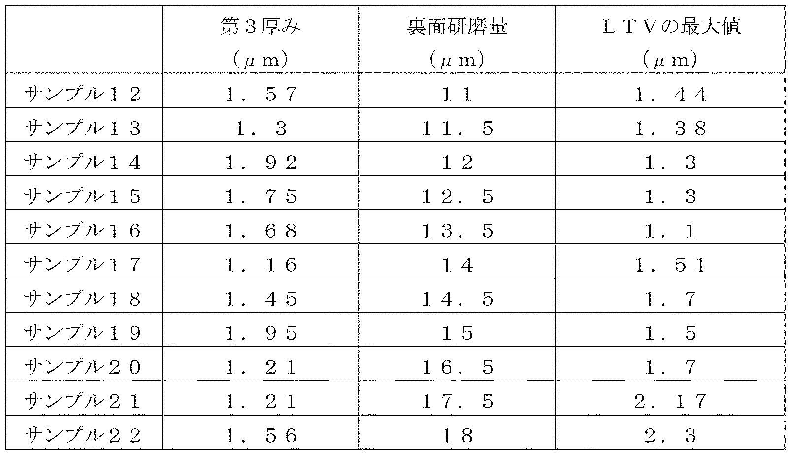
表2は、第3厚みH3が1μm以上2μm以下であった炭化珪素エピタキシャル基板100におけるLTVの最大値を示している。表2に示されるように、第3厚みH3が1μm以上2μm以下である場合、裏面研磨量H4が11μm以上16.5μm以下とされた炭化珪素エピタキシャル基板100(サンプル12から20)におけるLTVの最大値は、2.0μm以下であった。具体的には、サンプル12から20に係る炭化珪素エピタキシャル基板100におけるLTVの最大値は、1.7μm以下であった。第3厚みH3が1μm以上2μm以下である場合、裏面研磨量H4が11μm以上13.5μm以下とされた炭化珪素エピタキシャル基板100(サンプル12から16)におけるLTVの最大値は、1.44μm以下であった。一方で、第3厚みH3が1μm以上2μm以下である場合、裏面研磨量H4が17.5μm以上とされた炭化珪素エピタキシャル基板100(サンプル21および22)におけるLTVの最大値は、2.1μm以上であった。
以上の結果より、比較例の炭化珪素エピタキシャル基板100と比較して、実施例の炭化珪素エピタキシャル基板100においては、LTVの最大値が低減されていることが確認できた。
今回開示された実施形態および実施例はすべての点で例示であって、制限的なものではないと考えられるべきである。本発明の範囲は上記した実施形態ではなく請求の範囲によって示され、請求の範囲と均等の意味、および範囲内でのすべての変更が含まれることが意図される。
1 第1主面、2 第2主面、3 第3主面、5 界面、6 外縁、7 オリエンテーションフラット部、8 円弧状部、9 外周側面、11 外周領域、12 中央領域、30 炭化珪素基板、31 第1炭化珪素基板、32 第2炭化珪素基板、40 炭化珪素エピタキシャル層、41 バッファ層、42 ドリフト層、50 正方領域、51 第1正方領域、52 第2正方領域、53 側壁面、54 底壁面、56 トレンチ、60 突起、61 頂点、62 第1裏面、63 第1表面、64 第2裏面、65 第2表面、66 凸面、67 凹部、69 凹面、71 第1炭化珪素エピタキシャル層、72 第2炭化珪素エピタキシャル層、73 第3炭化珪素エピタキシャル層、74 第4炭化珪素エピタキシャル層、81 第1平坦面、82 第2平坦面、83 第3平坦面、90 炭化珪素粒子、91 三角欠陥、92 底面部、93 端点、94 底辺部、95 第1辺部、96 第2辺部、99 仮想直線、100 炭化珪素エピタキシャル基板、101 第1方向、102 第2方向、103 第3方向、113 ボディ領域、114 ソース領域、115 ゲート絶縁膜、116 ソース電極、117 マスク、118 コンタクト領域、119 ソース配線、123 ドレイン電極、126 層間絶縁膜、127 ゲート電極(電極)、200 製造装置、201 反応室、202 ステージ、203 発熱体、204 石英管、205 内壁面、207 ガス導入口、208 ガス排気口、209 回転軸、210 サセプタ、231 第1ガス供給部、232 第2ガス供給部、233 第3ガス供給部、234 第4ガス供給部、235 ガス供給部、241 第1ガス流量制御部、242 第2ガス流量制御部、243 第3ガス流量制御部、244 第4ガス流量制御部、245 制御部、300 機械研磨装置、301 定盤、302 研磨ヘッド、310 スラリー、312 砥粒、400 炭化珪素半導体装置、A 測定面、B 吸着面、C1 第1長さ、C2 第2長さ、D1 高さ、D2 深さ、E 距離、F1 第1幅、F2 第2幅、H1 第1厚み、H2 第2厚み、H3 第3厚み(厚み)、H4 裏面研磨量(研磨量)、L1 第1平面、L2 第2平面、O 中心、P1 最高点、P2 最低点、T1 最高高さ、T2 最低高さ、W 最大径、θ オフ角。
Claims (9)
- 炭化珪素基板と、
前記炭化珪素基板上に設けられている炭化珪素エピタキシャル層とを備え、
前記炭化珪素エピタキシャル層は、前記炭化珪素基板と前記炭化珪素エピタキシャル層との界面の反対にある第1主面を含み、
前記第1主面において、炭化珪素によって構成されている突起があり、
前記第1主面は、外縁と、前記外縁から3mm以内の領域である外周領域と、前記外周領域に取り囲まれた中央領域とによって構成されており、
前記中央領域を1辺の長さが10mmである複数の正方領域に区分した場合、前記複数の正方領域は、前記突起に最も近い第1正方領域と、前記第1正方領域以外の前記複数の正方領域である複数の第2正方領域とによって構成されており、
前記第1正方領域のLTVは、前記複数の第2正方領域の各々のLTVよりも大きく、
前記第1正方領域のLTVは、2μm以下である、炭化珪素エピタキシャル基板。 - 前記第1正方領域のLTVは、1.5μm以下である、請求項1に記載の炭化珪素エピタキシャル基板。
- 前記炭化珪素エピタキシャル層の厚みは、10μm以上30μm以下である、請求項1または請求項2に記載の炭化珪素エピタキシャル基板。
- 炭化珪素基板と、
前記炭化珪素基板上に設けられている炭化珪素エピタキシャル層と、を備え、
前記炭化珪素エピタキシャル層は、前記炭化珪素基板と前記炭化珪素エピタキシャル層との界面の反対にある第1主面を含み、
前記炭化珪素基板は、前記界面の反対にある第2主面を含み、
前記第2主面は、研磨面であり、
前記第1主面は、外縁と、前記外縁から3mm以内の領域である外周領域と、前記外周領域に取り囲まれた中央領域とによって構成されており、
前記中央領域を1辺の長さが10mmである複数の正方領域に区分した場合、
前記複数の正方領域におけるLTVの最大値は、2μm以下である、炭化珪素エピタキシャル基板。 - 前記複数の正方領域におけるLTVの最大値は、1.5μm以下である、請求項4に記載の炭化珪素エピタキシャル基板。
- 第1裏面と前記第1裏面の反対にある第1表面とを含む第1炭化珪素基板を準備する工程と、
前記第1裏面に炭化珪素粒子を付着させる工程と、
前記第1表面に接している第1炭化珪素エピタキシャル層を形成し且つ前記第1裏面および前記炭化珪素粒子に接している第2炭化珪素エピタキシャル層を形成する工程とを備え、
前記第1炭化珪素エピタキシャル層および前記第2炭化珪素エピタキシャル層を形成する工程において、前記炭化珪素粒子を起点として前記第2炭化珪素エピタキシャル層に三角欠陥が形成され、
前記第2炭化珪素エピタキシャル層にある前記三角欠陥を用いて前記第2炭化珪素エピタキシャル層の厚みを測定する工程と、
測定された前記第2炭化珪素エピタキシャル層の厚みに基づいて研磨量を決定する工程と、
第2裏面と前記第2裏面の反対にある第2表面とを含む第2炭化珪素基板を準備する工程と、
前記第2表面に接している第3炭化珪素エピタキシャル層を形成し且つ前記第2裏面に接している第4炭化珪素エピタキシャル層を形成する工程と、
前記研磨量に基づいて前記第4炭化珪素エピタキシャル層を研磨により除去する工程とをさらに備えた、炭化珪素エピタキシャル基板の製造方法。 - 前記第2炭化珪素エピタキシャル層の厚みは、1μm未満であり、
前記研磨量は8.5μm以上12.5μm以下である、請求項6に記載の炭化珪素エピタキシャル基板の製造方法。 - 前記第2炭化珪素エピタキシャル層の厚みは、1μm以上2μm以下であり、
前記研磨量は11μm以上16.5μm以下である、請求項6に記載の炭化珪素エピタキシャル基板の製造方法。 - 請求項1から請求項5のいずれか1項に記載の炭化珪素エピタキシャル基板を準備する工程と、
前記炭化珪素エピタキシャル層上に電極を形成する工程とを備えた、炭化珪素半導体装置の製造方法。
Priority Applications (1)
| Application Number | Priority Date | Filing Date | Title |
|---|---|---|---|
| JP2025529610A JPWO2025004787A1 (ja) | 2023-06-29 | 2024-06-11 |
Applications Claiming Priority (2)
| Application Number | Priority Date | Filing Date | Title |
|---|---|---|---|
| JP2023107032 | 2023-06-29 | ||
| JP2023-107032 | 2023-06-29 |
Publications (1)
| Publication Number | Publication Date |
|---|---|
| WO2025004787A1 true WO2025004787A1 (ja) | 2025-01-02 |
Family
ID=93938790
Family Applications (1)
| Application Number | Title | Priority Date | Filing Date |
|---|---|---|---|
| PCT/JP2024/021156 Ceased WO2025004787A1 (ja) | 2023-06-29 | 2024-06-11 | 炭化珪素エピタキシャル基板、炭化珪素エピタキシャル基板の製造方法および炭化珪素半導体装置の製造方法 |
Country Status (2)
| Country | Link |
|---|---|
| JP (1) | JPWO2025004787A1 (ja) |
| WO (1) | WO2025004787A1 (ja) |
Citations (2)
| Publication number | Priority date | Publication date | Assignee | Title |
|---|---|---|---|---|
| JP2016501809A (ja) * | 2012-10-26 | 2016-01-21 | ダウ コーニング コーポレーションDow Corning Corporation | 平坦なSiC半導体基板 |
| JP2017183729A (ja) * | 2017-04-25 | 2017-10-05 | 住友電気工業株式会社 | 炭化珪素半導体基板およびその製造方法、ならびに炭化珪素半導体装置の製造方法 |
-
2024
- 2024-06-11 WO PCT/JP2024/021156 patent/WO2025004787A1/ja not_active Ceased
- 2024-06-11 JP JP2025529610A patent/JPWO2025004787A1/ja active Pending
Patent Citations (2)
| Publication number | Priority date | Publication date | Assignee | Title |
|---|---|---|---|---|
| JP2016501809A (ja) * | 2012-10-26 | 2016-01-21 | ダウ コーニング コーポレーションDow Corning Corporation | 平坦なSiC半導体基板 |
| JP2017183729A (ja) * | 2017-04-25 | 2017-10-05 | 住友電気工業株式会社 | 炭化珪素半導体基板およびその製造方法、ならびに炭化珪素半導体装置の製造方法 |
Also Published As
| Publication number | Publication date |
|---|---|
| JPWO2025004787A1 (ja) | 2025-01-02 |
Similar Documents
| Publication | Publication Date | Title |
|---|---|---|
| CN107833829B (zh) | 碳化硅半导体衬底 | |
| CN107532327B (zh) | 碳化硅单晶衬底、碳化硅半导体器件以及制造碳化硅半导体器件的方法 | |
| CN106232877A (zh) | 制造碳化硅晶锭的方法、碳化硅种衬底、碳化硅衬底、半导体器件和制造半导体器件的方法 | |
| US12270122B2 (en) | Silicon carbide wafer and semiconductor device | |
| CN110214363A (zh) | 碳化硅外延衬底和制造碳化硅半导体器件的方法 | |
| US20240332364A1 (en) | Silicon carbide epitaxial substrate, method of manufacturing silicon carbide epitaxial substrate, and method of manufacturing silicon carbide semiconductor device | |
| JP7400715B2 (ja) | 炭化珪素エピタキシャル基板および炭化珪素半導体装置の製造方法 | |
| JP7831290B2 (ja) | 炭化珪素エピタキシャル基板および炭化珪素エピタキシャル基板の製造方法 | |
| JP2015207695A (ja) | エピタキシャルウエハの製造方法およびエピタキシャルウエハ | |
| JP7310822B2 (ja) | 炭化珪素エピタキシャル基板の製造方法および炭化珪素半導体装置の製造方法 | |
| WO2025004787A1 (ja) | 炭化珪素エピタキシャル基板、炭化珪素エピタキシャル基板の製造方法および炭化珪素半導体装置の製造方法 | |
| JP7772061B2 (ja) | 炭化珪素エピタキシャル基板および炭化珪素半導体装置の製造方法 | |
| US20240363696A1 (en) | Silicon carbide epitaxial substrate and method of manufacturing silicon carbide semiconductor device | |
| WO2024058044A1 (ja) | 炭化珪素エピタキシャル基板、エピタキシャル基板の製造方法および炭化珪素半導体装置の製造方法 | |
| JP7711396B2 (ja) | 炭化珪素エピタキシャル基板および炭化珪素半導体装置 | |
| JP7255473B2 (ja) | 炭化ケイ素多結晶基板の製造方法 | |
| JP2020111495A (ja) | 炭化珪素多結晶基板、炭化珪素多結晶膜の製造方法および炭化珪素多結晶基板の製造方法 | |
| TWI776220B (zh) | 磊晶晶圓、晶圓及其製造方法 | |
| WO2024127944A1 (ja) | 炭化珪素エピタキシャル基板、炭化珪素半導体装置の製造方法および炭化珪素エピタキシャル基板の製造方法 | |
| JP7661771B2 (ja) | 炭化珪素エピタキシャル基板の製造方法および炭化珪素半導体装置の製造方法 | |
| WO2024257580A1 (ja) | 炭化珪素エピタキシャル基板、炭化珪素半導体装置の製造方法および炭化珪素エピタキシャル基板の製造方法 | |
| US20250393275A1 (en) | Silicon carbide epitaxial substrate and method of manufacturing silicon carbide semiconductor device | |
| JP7131146B2 (ja) | 炭化珪素エピタキシャル基板の製造方法および炭化珪素半導体装置の製造方法 | |
| JP7115084B2 (ja) | 炭化珪素エピタキシャル基板の製造方法および炭化珪素半導体装置の製造方法 | |
| WO2024232252A1 (ja) | 炭化珪素エピタキシャル基板および炭化珪素半導体装置の製造方法 |
Legal Events
| Date | Code | Title | Description |
|---|---|---|---|
| 121 | Ep: the epo has been informed by wipo that ep was designated in this application |
Ref document number: 24831654 Country of ref document: EP Kind code of ref document: A1 |
|
| ENP | Entry into the national phase |
Ref document number: 2025529610 Country of ref document: JP Kind code of ref document: A |
|
| NENP | Non-entry into the national phase |
Ref country code: DE |