WO2025004571A1 - 半導体装置 - Google Patents
半導体装置 Download PDFInfo
- Publication number
- WO2025004571A1 WO2025004571A1 PCT/JP2024/017779 JP2024017779W WO2025004571A1 WO 2025004571 A1 WO2025004571 A1 WO 2025004571A1 JP 2024017779 W JP2024017779 W JP 2024017779W WO 2025004571 A1 WO2025004571 A1 WO 2025004571A1
- Authority
- WO
- WIPO (PCT)
- Prior art keywords
- region
- gate
- view
- plan
- semiconductor device
- Prior art date
- Legal status (The legal status is an assumption and is not a legal conclusion. Google has not performed a legal analysis and makes no representation as to the accuracy of the status listed.)
- Ceased
Links
Images







Classifications
-
- H—ELECTRICITY
- H10—SEMICONDUCTOR DEVICES; ELECTRIC SOLID-STATE DEVICES NOT OTHERWISE PROVIDED FOR
- H10D—INORGANIC ELECTRIC SEMICONDUCTOR DEVICES
- H10D84/00—Integrated devices formed in or on semiconductor substrates that comprise only semiconducting layers, e.g. on Si wafers or on GaAs-on-Si wafers
- H10D84/80—Integrated devices formed in or on semiconductor substrates that comprise only semiconducting layers, e.g. on Si wafers or on GaAs-on-Si wafers characterised by the integration of at least one component covered by groups H10D12/00 or H10D30/00, e.g. integration of IGFETs
- H10D84/82—Integrated devices formed in or on semiconductor substrates that comprise only semiconducting layers, e.g. on Si wafers or on GaAs-on-Si wafers characterised by the integration of at least one component covered by groups H10D12/00 or H10D30/00, e.g. integration of IGFETs of only field-effect components
- H10D84/83—Integrated devices formed in or on semiconductor substrates that comprise only semiconducting layers, e.g. on Si wafers or on GaAs-on-Si wafers characterised by the integration of at least one component covered by groups H10D12/00 or H10D30/00, e.g. integration of IGFETs of only field-effect components of only insulated-gate FETs [IGFET]
-
- H—ELECTRICITY
- H10—SEMICONDUCTOR DEVICES; ELECTRIC SOLID-STATE DEVICES NOT OTHERWISE PROVIDED FOR
- H10W—GENERIC PACKAGES, INTERCONNECTIONS, CONNECTORS OR OTHER CONSTRUCTIONAL DETAILS OF DEVICES COVERED BY CLASS H10
- H10W20/00—Interconnections in chips, wafers or substrates
- H10W20/40—Interconnections external to wafers or substrates, e.g. back-end-of-line [BEOL] metallisations or vias connecting to gate electrodes
- H10W20/41—Interconnections external to wafers or substrates, e.g. back-end-of-line [BEOL] metallisations or vias connecting to gate electrodes characterised by their conductive parts
- H10W20/435—Cross-sectional shapes or dispositions of interconnections
-
- H—ELECTRICITY
- H10—SEMICONDUCTOR DEVICES; ELECTRIC SOLID-STATE DEVICES NOT OTHERWISE PROVIDED FOR
- H10D—INORGANIC ELECTRIC SEMICONDUCTOR DEVICES
- H10D30/00—Field-effect transistors [FET]
- H10D30/60—Insulated-gate field-effect transistors [IGFET]
- H10D30/63—Vertical IGFETs
-
- H—ELECTRICITY
- H10—SEMICONDUCTOR DEVICES; ELECTRIC SOLID-STATE DEVICES NOT OTHERWISE PROVIDED FOR
- H10D—INORGANIC ELECTRIC SEMICONDUCTOR DEVICES
- H10D30/00—Field-effect transistors [FET]
- H10D30/60—Insulated-gate field-effect transistors [IGFET]
- H10D30/64—Double-diffused metal-oxide semiconductor [DMOS] FETs
- H10D30/66—Vertical DMOS [VDMOS] FETs
- H10D30/668—Vertical DMOS [VDMOS] FETs having trench gate electrodes, e.g. UMOS transistors
-
- H—ELECTRICITY
- H10—SEMICONDUCTOR DEVICES; ELECTRIC SOLID-STATE DEVICES NOT OTHERWISE PROVIDED FOR
- H10D—INORGANIC ELECTRIC SEMICONDUCTOR DEVICES
- H10D62/00—Semiconductor bodies, or regions thereof, of devices having potential barriers
- H10D62/10—Shapes, relative sizes or dispositions of the regions of the semiconductor bodies; Shapes of the semiconductor bodies
- H10D62/102—Constructional design considerations for preventing surface leakage or controlling electric field concentration
- H10D62/103—Constructional design considerations for preventing surface leakage or controlling electric field concentration for increasing or controlling the breakdown voltage of reverse-biased devices
- H10D62/105—Constructional design considerations for preventing surface leakage or controlling electric field concentration for increasing or controlling the breakdown voltage of reverse-biased devices by having particular doping profiles, shapes or arrangements of PN junctions; by having supplementary regions, e.g. junction termination extension [JTE]
- H10D62/106—Constructional design considerations for preventing surface leakage or controlling electric field concentration for increasing or controlling the breakdown voltage of reverse-biased devices by having particular doping profiles, shapes or arrangements of PN junctions; by having supplementary regions, e.g. junction termination extension [JTE] having supplementary regions doped oppositely to or in rectifying contact with regions of the semiconductor bodies, e.g. guard rings with PN or Schottky junctions
-
- H—ELECTRICITY
- H10—SEMICONDUCTOR DEVICES; ELECTRIC SOLID-STATE DEVICES NOT OTHERWISE PROVIDED FOR
- H10D—INORGANIC ELECTRIC SEMICONDUCTOR DEVICES
- H10D62/00—Semiconductor bodies, or regions thereof, of devices having potential barriers
- H10D62/10—Shapes, relative sizes or dispositions of the regions of the semiconductor bodies; Shapes of the semiconductor bodies
- H10D62/124—Shapes, relative sizes or dispositions of the regions of semiconductor bodies or of junctions between the regions
- H10D62/126—Top-view geometrical layouts of the regions or the junctions
-
- H—ELECTRICITY
- H10—SEMICONDUCTOR DEVICES; ELECTRIC SOLID-STATE DEVICES NOT OTHERWISE PROVIDED FOR
- H10D—INORGANIC ELECTRIC SEMICONDUCTOR DEVICES
- H10D62/00—Semiconductor bodies, or regions thereof, of devices having potential barriers
- H10D62/10—Shapes, relative sizes or dispositions of the regions of the semiconductor bodies; Shapes of the semiconductor bodies
- H10D62/124—Shapes, relative sizes or dispositions of the regions of semiconductor bodies or of junctions between the regions
- H10D62/126—Top-view geometrical layouts of the regions or the junctions
- H10D62/127—Top-view geometrical layouts of the regions or the junctions of cellular field-effect devices, e.g. multicellular DMOS transistors or IGBTs
-
- H—ELECTRICITY
- H10—SEMICONDUCTOR DEVICES; ELECTRIC SOLID-STATE DEVICES NOT OTHERWISE PROVIDED FOR
- H10D—INORGANIC ELECTRIC SEMICONDUCTOR DEVICES
- H10D62/00—Semiconductor bodies, or regions thereof, of devices having potential barriers
- H10D62/40—Crystalline structures
-
- H—ELECTRICITY
- H10—SEMICONDUCTOR DEVICES; ELECTRIC SOLID-STATE DEVICES NOT OTHERWISE PROVIDED FOR
- H10D—INORGANIC ELECTRIC SEMICONDUCTOR DEVICES
- H10D62/00—Semiconductor bodies, or regions thereof, of devices having potential barriers
- H10D62/60—Impurity distributions or concentrations
-
- H—ELECTRICITY
- H10—SEMICONDUCTOR DEVICES; ELECTRIC SOLID-STATE DEVICES NOT OTHERWISE PROVIDED FOR
- H10D—INORGANIC ELECTRIC SEMICONDUCTOR DEVICES
- H10D64/00—Electrodes of devices having potential barriers
- H10D64/20—Electrodes characterised by their shapes, relative sizes or dispositions
- H10D64/23—Electrodes carrying the current to be rectified, amplified, oscillated or switched, e.g. sources, drains, anodes or cathodes
- H10D64/251—Source or drain electrodes for field-effect devices
- H10D64/252—Source or drain electrodes for field-effect devices for vertical or pseudo-vertical devices
- H10D64/2523—Source or drain electrodes for field-effect devices for vertical or pseudo-vertical devices for vertical devices wherein the source or drain electrodes extend entirely through semiconductor bodies
-
- H—ELECTRICITY
- H10—SEMICONDUCTOR DEVICES; ELECTRIC SOLID-STATE DEVICES NOT OTHERWISE PROVIDED FOR
- H10D—INORGANIC ELECTRIC SEMICONDUCTOR DEVICES
- H10D64/00—Electrodes of devices having potential barriers
- H10D64/20—Electrodes characterised by their shapes, relative sizes or dispositions
- H10D64/27—Electrodes not carrying the current to be rectified, amplified, oscillated or switched, e.g. gates
- H10D64/311—Gate electrodes for field-effect devices
- H10D64/411—Gate electrodes for field-effect devices for FETs
- H10D64/511—Gate electrodes for field-effect devices for FETs for IGFETs
- H10D64/512—Disposition of the gate electrodes, e.g. buried gates
- H10D64/513—Disposition of the gate electrodes, e.g. buried gates within recesses in the substrate, e.g. trench gates, groove gates or buried gates
-
- H—ELECTRICITY
- H10—SEMICONDUCTOR DEVICES; ELECTRIC SOLID-STATE DEVICES NOT OTHERWISE PROVIDED FOR
- H10D—INORGANIC ELECTRIC SEMICONDUCTOR DEVICES
- H10D8/00—Diodes
-
- H—ELECTRICITY
- H10—SEMICONDUCTOR DEVICES; ELECTRIC SOLID-STATE DEVICES NOT OTHERWISE PROVIDED FOR
- H10D—INORGANIC ELECTRIC SEMICONDUCTOR DEVICES
- H10D8/00—Diodes
- H10D8/20—Breakdown diodes, e.g. avalanche diodes
- H10D8/25—Zener diodes
-
- H—ELECTRICITY
- H10—SEMICONDUCTOR DEVICES; ELECTRIC SOLID-STATE DEVICES NOT OTHERWISE PROVIDED FOR
- H10D—INORGANIC ELECTRIC SEMICONDUCTOR DEVICES
- H10D8/00—Diodes
- H10D8/411—PN diodes having planar bodies
-
- H—ELECTRICITY
- H10—SEMICONDUCTOR DEVICES; ELECTRIC SOLID-STATE DEVICES NOT OTHERWISE PROVIDED FOR
- H10D—INORGANIC ELECTRIC SEMICONDUCTOR DEVICES
- H10D84/00—Integrated devices formed in or on semiconductor substrates that comprise only semiconducting layers, e.g. on Si wafers or on GaAs-on-Si wafers
- H10D84/80—Integrated devices formed in or on semiconductor substrates that comprise only semiconducting layers, e.g. on Si wafers or on GaAs-on-Si wafers characterised by the integration of at least one component covered by groups H10D12/00 or H10D30/00, e.g. integration of IGFETs
- H10D84/811—Combinations of field-effect devices and one or more diodes, capacitors or resistors
-
- H—ELECTRICITY
- H10—SEMICONDUCTOR DEVICES; ELECTRIC SOLID-STATE DEVICES NOT OTHERWISE PROVIDED FOR
- H10D—INORGANIC ELECTRIC SEMICONDUCTOR DEVICES
- H10D84/00—Integrated devices formed in or on semiconductor substrates that comprise only semiconducting layers, e.g. on Si wafers or on GaAs-on-Si wafers
- H10D84/80—Integrated devices formed in or on semiconductor substrates that comprise only semiconducting layers, e.g. on Si wafers or on GaAs-on-Si wafers characterised by the integration of at least one component covered by groups H10D12/00 or H10D30/00, e.g. integration of IGFETs
- H10D84/82—Integrated devices formed in or on semiconductor substrates that comprise only semiconducting layers, e.g. on Si wafers or on GaAs-on-Si wafers characterised by the integration of at least one component covered by groups H10D12/00 or H10D30/00, e.g. integration of IGFETs of only field-effect components
- H10D84/83—Integrated devices formed in or on semiconductor substrates that comprise only semiconducting layers, e.g. on Si wafers or on GaAs-on-Si wafers characterised by the integration of at least one component covered by groups H10D12/00 or H10D30/00, e.g. integration of IGFETs of only field-effect components of only insulated-gate FETs [IGFET]
- H10D84/83125—Integrated devices formed in or on semiconductor substrates that comprise only semiconducting layers, e.g. on Si wafers or on GaAs-on-Si wafers characterised by the integration of at least one component covered by groups H10D12/00 or H10D30/00, e.g. integration of IGFETs of only field-effect components of only insulated-gate FETs [IGFET] the IGFETs characterised by having shared source or drain regions
-
- H—ELECTRICITY
- H10—SEMICONDUCTOR DEVICES; ELECTRIC SOLID-STATE DEVICES NOT OTHERWISE PROVIDED FOR
- H10D—INORGANIC ELECTRIC SEMICONDUCTOR DEVICES
- H10D84/00—Integrated devices formed in or on semiconductor substrates that comprise only semiconducting layers, e.g. on Si wafers or on GaAs-on-Si wafers
- H10D84/80—Integrated devices formed in or on semiconductor substrates that comprise only semiconducting layers, e.g. on Si wafers or on GaAs-on-Si wafers characterised by the integration of at least one component covered by groups H10D12/00 or H10D30/00, e.g. integration of IGFETs
- H10D84/82—Integrated devices formed in or on semiconductor substrates that comprise only semiconducting layers, e.g. on Si wafers or on GaAs-on-Si wafers characterised by the integration of at least one component covered by groups H10D12/00 or H10D30/00, e.g. integration of IGFETs of only field-effect components
- H10D84/83—Integrated devices formed in or on semiconductor substrates that comprise only semiconducting layers, e.g. on Si wafers or on GaAs-on-Si wafers characterised by the integration of at least one component covered by groups H10D12/00 or H10D30/00, e.g. integration of IGFETs of only field-effect components of only insulated-gate FETs [IGFET]
- H10D84/837—Integrated devices formed in or on semiconductor substrates that comprise only semiconducting layers, e.g. on Si wafers or on GaAs-on-Si wafers characterised by the integration of at least one component covered by groups H10D12/00 or H10D30/00, e.g. integration of IGFETs of only field-effect components of only insulated-gate FETs [IGFET] comprising vertical IGFETs
-
- H—ELECTRICITY
- H10—SEMICONDUCTOR DEVICES; ELECTRIC SOLID-STATE DEVICES NOT OTHERWISE PROVIDED FOR
- H10D—INORGANIC ELECTRIC SEMICONDUCTOR DEVICES
- H10D89/00—Aspects of integrated devices not covered by groups H10D84/00 - H10D88/00
- H10D89/60—Integrated devices comprising arrangements for electrical or thermal protection, e.g. protection circuits against electrostatic discharge [ESD]
- H10D89/601—Integrated devices comprising arrangements for electrical or thermal protection, e.g. protection circuits against electrostatic discharge [ESD] for devices having insulated gate electrodes, e.g. for IGFETs or IGBTs
- H10D89/611—Integrated devices comprising arrangements for electrical or thermal protection, e.g. protection circuits against electrostatic discharge [ESD] for devices having insulated gate electrodes, e.g. for IGFETs or IGBTs using diodes as protective elements
-
- H—ELECTRICITY
- H10—SEMICONDUCTOR DEVICES; ELECTRIC SOLID-STATE DEVICES NOT OTHERWISE PROVIDED FOR
- H10D—INORGANIC ELECTRIC SEMICONDUCTOR DEVICES
- H10D89/00—Aspects of integrated devices not covered by groups H10D84/00 - H10D88/00
- H10D89/60—Integrated devices comprising arrangements for electrical or thermal protection, e.g. protection circuits against electrostatic discharge [ESD]
- H10D89/601—Integrated devices comprising arrangements for electrical or thermal protection, e.g. protection circuits against electrostatic discharge [ESD] for devices having insulated gate electrodes, e.g. for IGFETs or IGBTs
- H10D89/911—Integrated devices comprising arrangements for electrical or thermal protection, e.g. protection circuits against electrostatic discharge [ESD] for devices having insulated gate electrodes, e.g. for IGFETs or IGBTs using passive elements as protective elements
-
- H—ELECTRICITY
- H10—SEMICONDUCTOR DEVICES; ELECTRIC SOLID-STATE DEVICES NOT OTHERWISE PROVIDED FOR
- H10W—GENERIC PACKAGES, INTERCONNECTIONS, CONNECTORS OR OTHER CONSTRUCTIONAL DETAILS OF DEVICES COVERED BY CLASS H10
- H10W90/00—Package configurations
-
- H—ELECTRICITY
- H10—SEMICONDUCTOR DEVICES; ELECTRIC SOLID-STATE DEVICES NOT OTHERWISE PROVIDED FOR
- H10D—INORGANIC ELECTRIC SEMICONDUCTOR DEVICES
- H10D1/00—Resistors, capacitors or inductors
- H10D1/40—Resistors
- H10D1/47—Resistors having no potential barriers
-
- H—ELECTRICITY
- H10—SEMICONDUCTOR DEVICES; ELECTRIC SOLID-STATE DEVICES NOT OTHERWISE PROVIDED FOR
- H10D—INORGANIC ELECTRIC SEMICONDUCTOR DEVICES
- H10D30/00—Field-effect transistors [FET]
- H10D30/60—Insulated-gate field-effect transistors [IGFET]
- H10D30/64—Double-diffused metal-oxide semiconductor [DMOS] FETs
- H10D30/66—Vertical DMOS [VDMOS] FETs
- H10D30/663—Vertical DMOS [VDMOS] FETs having both source contacts and drain contacts on the same surface, i.e. up-drain VDMOS
-
- H—ELECTRICITY
- H10—SEMICONDUCTOR DEVICES; ELECTRIC SOLID-STATE DEVICES NOT OTHERWISE PROVIDED FOR
- H10D—INORGANIC ELECTRIC SEMICONDUCTOR DEVICES
- H10D62/00—Semiconductor bodies, or regions thereof, of devices having potential barriers
- H10D62/10—Shapes, relative sizes or dispositions of the regions of the semiconductor bodies; Shapes of the semiconductor bodies
- H10D62/17—Semiconductor regions connected to electrodes not carrying current to be rectified, amplified or switched, e.g. channel regions
- H10D62/393—Body regions of DMOS transistors or IGBTs
-
- H—ELECTRICITY
- H10—SEMICONDUCTOR DEVICES; ELECTRIC SOLID-STATE DEVICES NOT OTHERWISE PROVIDED FOR
- H10W—GENERIC PACKAGES, INTERCONNECTIONS, CONNECTORS OR OTHER CONSTRUCTIONAL DETAILS OF DEVICES COVERED BY CLASS H10
- H10W72/00—Interconnections or connectors in packages
- H10W72/90—Bond pads, in general
- H10W72/941—Dispositions of bond pads
- H10W72/9415—Dispositions of bond pads relative to the surface, e.g. recessed, protruding
Definitions
- This disclosure relates to semiconductor devices, and in particular to chip-size package type semiconductor devices.
- the semiconductor device configured as described above can achieve miniaturization of circuits using vertical MOS transistors.
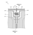
- FIG. 1 is a schematic cross-sectional view showing an example of a structure of a semiconductor device according to an embodiment.
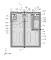
- FIG. 2A is a schematic plan view showing an example of a structure of a semiconductor device according to an embodiment.
- FIG. 2B is a schematic plan view showing an example of the structure of the semiconductor device according to the embodiment.
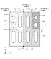
- FIG. 3A is a schematic plan view showing an example of a part of the structure of the semiconductor device according to the embodiment.
- FIG. 3B is a schematic cross-sectional view showing an example of a part of the structure of the semiconductor device according to the embodiment.
- FIG. 3C is a schematic cross-sectional view showing an example of a part of the structure of the semiconductor device according to the embodiment.
- FIG. 4A is a schematic plan view showing an example of a part of the structure of the semiconductor device according to the embodiment.
- FIG. 4B is a schematic cross-sectional view showing an example of a part of the structure of the semiconductor device according to the embodiment.
- FIG. 4C is a schematic cross-sectional view showing an example of a part of the structure of the semiconductor device according to the embodiment.
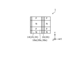
- FIG. 5A is a schematic plan view of a general unit configuration of a first transistor according to an embodiment.
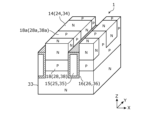
- FIG. 5B is a schematic perspective view of a general unit configuration of a first transistor according to the embodiment.
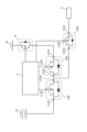
- FIG. 6 is a circuit diagram showing an example of use of the semiconductor device according to the embodiment.
- FIG. 7 is a circuit diagram showing an example of use of a semiconductor device according to a comparative example.
- FIG. 8A is a schematic plan view illustrating an example of the structure of a transistor according to a comparative example.
- FIG. 8B is a schematic plan view illustrating an example of the structure of a transistor according to a comparative example.
- FIG. 9A is a schematic plan view illustrating an example of the structure of a transistor according to a comparative example.
- FIG. 9B is a schematic plan view illustrating an example of the structure of a transistor according to a comparative example.
- FIG. 10A is a schematic plan view showing a modified example of the structure of the semiconductor device according to the embodiment.
- FIG. 10B is a schematic plan view showing a modified example of the structure of the semiconductor device according to the embodiment.
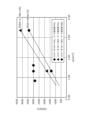
- FIG. 11 is a graph plotting the relationship between the area of a transistor in a plan view and the ESD resistance.
- a and B are electrically connected includes cases where A and B are directly connected via wiring, where A and B are directly connected without wiring, and where A and B are indirectly connected via a resistance component (resistance element, resistance wiring).
- the semiconductor device according to an embodiment is a chip size package (CSP) type semiconductor device that has a dual configuration in which two vertical MOS (Metal Oxide Semiconductor) transistors are formed on a semiconductor substrate and can be mounted face-down.
- the two vertical MOS transistors are power transistors, so-called trench MOS type FETs (Field Effect Transistors).
- FIG. 1 is a schematic cross-sectional view showing an example of the structure of a semiconductor device 1 according to an embodiment.
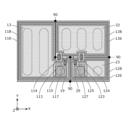
- FIGS. 2A and 2B are schematic plan views showing an example of the structure of a semiconductor device 1 according to an embodiment.
- the size and shape of the semiconductor device 1 in FIGS. 2A and 2B are examples.
- the size, shape, and arrangement of the pads and electrodes are also examples.
- FIG. 2B shows the state immediately after the formation of portion 13 of the first source electrode 11, first gate electrode 19, first gate wiring 118, portion 23 of the second source electrode 21, second gate electrode 29, second gate wiring 128, portion 33 of the third source electrode 31, and third gate wiring 138 on the surface side of the semiconductor layer 40. Pads that should not be visible at this point are shown with dotted lines. Each component will be described later.
- FIG. 1 shows a cross section of semiconductor device 1 taken along line I-I in FIG. 2A.
- the semiconductor device 1 has a semiconductor substrate 42, a metal layer 41, and a low-concentration impurity layer 43 formed on the semiconductor substrate 42.
- the semiconductor substrate 42 and the low-concentration impurity layer 43 are collectively referred to as the semiconductor layer 40.
- the semiconductor substrate 42 is disposed on the back surface side of the semiconductor layer 40 and is made of silicon of a first conductivity type containing an impurity of a first concentration.
- the semiconductor layer 40 has a low-concentration impurity layer 43 of the first conductivity type formed in contact with the semiconductor substrate 42 and containing an impurity of a second concentration lower than the first concentration.
- the low-concentration impurity layer 43 is formed on the semiconductor substrate 42 by, for example, epitaxial growth.
- the semiconductor device 1 has a first vertical MOS transistor 10 (hereinafter also referred to as “transistor 10") entirely formed in a first region A1 of the semiconductor layer 40, a second vertical MOS transistor 20 (hereinafter also referred to as “transistor 20”) entirely formed in a second region A2 of the semiconductor layer 40, and a third vertical MOS transistor 30 (hereinafter also referred to as "transistor 30") entirely formed in a third region A3 of the semiconductor layer 40.
- a first vertical MOS transistor 10 hereinafter also referred to as "transistor 10”
- second vertical MOS transistor 20 hereinafter also referred to as “transistor 20”
- a third vertical MOS transistor 30 hereinafter also referred to as "transistor 30”
- Transistor 10 formed entirely within the first region A1 means that, in a planar view, all of the elements constituting transistor 10 are contained within the first region A1 and are not contained in any region that is not the first region A1.
- transistor 20 formed entirely within the second region A2 means that, in a planar view, all of the elements constituting transistor 20 are contained within the second region A2 and are not contained in any region that is not the second region A2.
- transistor 30 formed entirely within the third region A3 means that, in a planar view, all of the elements constituting transistor 30 are contained within the third region A3 and are not contained in any region that is not the third region A3.
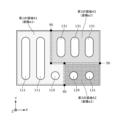
- the surface side of the semiconductor layer 40 is divided into a first region A1, a second region A2, and a third region A3 in a plan view, which do not overlap with each other and are not disposed separately.
- the fact that the first region A1, the second region A2, and the third region A3 are not disposed separately means that the first region A1, the second region A2, and the third region A3 do not include any enclaves.
- a virtual boundary line 90 that divides the first region A1, the second region A2, and the third region A3 is shown by a dotted line.
- the dotted line indicating the boundary line 90 is shown extending to the outside of the semiconductor layer 40, but the actual boundary line 90 terminates at the outer periphery of the semiconductor layer 40 in a plan view (for convenience, the ends of the boundary line 90 are shown as P1, P2, P3, and P4, respectively, in FIG. 2A and FIG. 2B).
- the boundary line 90 will be described later.
- the dashed lines indicating the first region A1, the second region A2, and the third region A3 are not exactly aligned with the outer periphery of the semiconductor layer 40 and the boundary line 90 for ease of understanding, but are drawn with some space between them.
- the outer periphery of the first region A1, the outer periphery of the second region A2, and the outer periphery of the third region A3 essentially coincide with the outer periphery of the semiconductor layer 40 and the boundary line 90.
- the metal layer 41 is formed in contact with the back side of the semiconductor layer 40, and may be made of silver (Ag) or copper (Cu), as a non-limiting example. Note that the metal layer 41 may contain trace amounts of elements other than metals that are mixed in as impurities during the manufacturing process of the metal material.
- a first body region 18 of a second conductivity type different from the first conductivity type is formed in the first region A1 of the low-concentration impurity layer 43.
- a first source region 14 of the first conductivity type is formed in the first body region 18.
- the first region A1 also has a plurality of first gate trenches 17 formed to a depth that penetrates from the upper surface of the semiconductor layer 40 through the first source region 14 and the first body region 18 to a portion of the low-concentration impurity layer 43, and a first gate conductor 15 is formed on the first gate insulating film 16 inside the first gate trench 17.
- the first gate conductor 15 is a buried gate electrode buried inside the semiconductor layer 40.
- the first gate conductor 15 is electrically connected to the first gate electrode 19 via the first gate wiring 118 (see FIG. 2B).
- the first source electrode 11 consists of a portion 12 and a portion 13, and the portion 12 is connected to the first source region 14 and the first body region 18 via the portion 13.
- the portion 12 of the first source electrode 11 is a layer that is joined with the solder during reflow in face-down mounting, and may be made of a metal material including, by way of non-limiting example, any one or more of nickel, titanium, tungsten, and palladium.
- the surface of the portion 12 may be plated with gold or the like.
- Part 13 of the first source electrode 11 is a layer that connects part 12 and the semiconductor layer 40, and may be made of a metal material including, by way of non-limiting example, any one or more of aluminum, copper, gold, and silver.
- the first gate electrode 19 may be formed simultaneously with the first source electrode 11, and may be formed with the same configuration and/or the same material as the first source electrode 11.
- the first gate wiring 118 is disposed so as to surround the portion 13 of the first source electrode 11 and the first gate electrode 19 in a plan view.
- the first gate wiring 118 is connected in series with the first gate electrode 19 via the first gate resistance element 117.
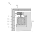
- FIG. 3B shows a schematic cross-sectional view including the first gate resistance element 117.
- FIG. 3B is a cut surface of the semiconductor device 1 taken along II-II in FIG. 3A
- FIG. 3A is a schematic plan view showing an enlarged view of the area A11 enclosed by the dashed line in FIG. 2B.
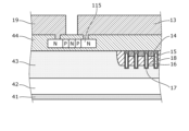
- FIG. 3C shows a schematic cross-sectional view including first Zener diode 115.
- FIG. 3C is a cut surface when semiconductor device 1 is cut along III-III in FIG. 3A.
- First gate electrode 19 and portion 13 of first source electrode 11 are electrically connected via first Zener diode 115.
- the gate resistor element and the Zener diode are both installed with the expectation of a protective function that prevents the transistor from being destroyed when an excessive voltage is applied to the gate electrode. In other words, they are elements installed to increase ESD (Electrostatic Discharge) resistance.
- the first gate resistor element 117 and the first Zener diode 115 may both be formed, for example, by injecting impurities into polysilicon. By controlling the type, amount, and position of the impurities, respectively, it is possible to control the resistivity of the first gate resistor element 117 and the position, number, and electrical direction of the PN junction in the first Zener diode 115.
- the first Zener diode 115 may be formed, for example as shown in FIG. 3C, with alternating portions where a first conductivity type impurity is injected to become the first conductivity type and portions where a second conductivity type impurity is injected to become the second conductivity type.
- two PN junctions are formed in both directions by the first Zener diode 115 between the first gate electrode 19 and portion 13 of the first source electrode 11.
- a first EQR (EQUI potential ring) 116 electrically connected to the semiconductor substrate 42 may be provided on the outer periphery of the first region A1.
- the first EQR 116 is provided in the hope of preventing leakage current from flowing between the outside and the first body region 18 of the transistor 10.
- the first EQR 116 may be made of a metal material including any one or more of aluminum, copper, gold, and silver.
- the semiconductor device 1 does not necessarily need to include a gate resistor element, a Zener diode, and an EQR.
- a second body region 28 of the second conductivity type is formed in the second region A2 of the low-concentration impurity layer 43.
- a second source region 24 of the first conductivity type is formed in the second body region 28.
- the second region A2 also has a plurality of second gate trenches 27 formed to a depth that penetrates from the upper surface of the semiconductor layer 40 through the second source region 24 and the second body region 28 to a portion of the low-concentration impurity layer 43, and further has a second gate conductor 25 formed on the second gate insulating film 26 inside the second gate trench 27.
- the second gate conductor 25 is a buried gate electrode buried inside the semiconductor layer 40.
- the second gate conductor 25 is electrically connected to the second gate electrode 29 via the second gate wiring 128 (see FIG. 2B).
- the second source electrode 21 consists of a portion 22 and a portion 23, and the portion 22 is connected to the second source region 24 and the second body region 28 via the portion 23.
- the portion 22 of the second source electrode 21 is a layer that is joined with the solder during reflow in face-down mounting, and may be made of a metal material including, by way of non-limiting example, any one or more of nickel, titanium, tungsten, and palladium.
- the surface of the portion 22 may be plated with gold or the like.
- Part 23 of the second source electrode 21 is a layer that connects part 22 and the semiconductor layer 40, and may be made of a metal material including, by way of non-limiting example, any one or more of aluminum, copper, gold, and silver.
- the second gate electrode 29 may be formed simultaneously with the second source electrode 21, and may be formed with the same configuration and/or the same material as the second source electrode 21.
- the second gate wiring 128 is disposed so as to surround the portion 23 of the second source electrode 21 and the second gate electrode 29 in a plan view.
- the second gate wiring 128 is connected in series with the second gate electrode 29 via the second gate resistor element 127.
- a second Zener diode 125 is provided between portion 23 of second source electrode 21 and second gate electrode 29. Second gate electrode 29 and portion 23 of second source electrode 21 are electrically connected via second Zener diode 125.
- the second gate resistor element 127 and the second Zener diode 125 may both be formed by, for example, injecting impurities into polysilicon. By controlling the type of impurity, the amount of impurity injected, and the position of the impurity injected, it is possible to control the resistivity of the second gate resistor element 127 and the position, number, and electrical direction of the PN junction in the second Zener diode 125.
- the second Zener diode 125 may have a structure similar to that of the first Zener diode 115, for example, as shown in FIG. 3C.
- a second EQR 126 electrically connected to the semiconductor substrate 42 may be provided on the outer periphery of the second region A2.
- the second EQR 126 is provided in the hope of preventing leakage current from flowing between the outside and the second body region 28 of the transistor 20.
- the second EQR 126 may be made of a metal material including any one or more of aluminum, copper, gold, and silver.
- a third body region 38 of the second conductivity type is formed in the third region A3 of the low-concentration impurity layer 43.
- a third source region 34 of the first conductivity type is formed in the third body region 38.
- a plurality of third gate trenches 37 are formed in the third region A3, each of which is formed to a depth from the upper surface of the semiconductor layer 40 through the third source region 34 and the third body region 38 to a portion of the low-concentration impurity layer 43.
- a third gate conductor 35 is formed on the third gate insulating film 36 inside the third gate trench 37.
- the third gate conductor 35 is a buried gate electrode buried inside the semiconductor layer 40.
- the third gate conductor 35 is electrically connected to the third gate wiring 138 (see FIG. 2B).
- the third source electrode 31 consists of a portion 32 and a portion 33, and the portion 32 is connected to the third source region 34 and the third body region 38 via the portion 33.
- the portion 32 of the third source electrode 31 is a layer that is joined with the solder during reflow in face-down mounting, and may be made of a metal material including, by way of non-limiting example, any one or more of nickel, titanium, tungsten, and palladium.
- the surface of the portion 32 may be plated with gold or the like.
- Part 33 of the third source electrode 31 is a layer that connects part 32 and the semiconductor layer 40, and may be made of a metal material including, as a non-limiting example, any one or more of aluminum, copper, gold, and silver.
- a third EQR 136 electrically connected to the semiconductor substrate 42 may be provided on the outer periphery of the third region A3.
- the third EQR 136 is provided in the hope of preventing leakage current from flowing between the outside and the third body region 38 of the transistor 30.
- the third EQR 136 may be made of a metal material including any one or more of aluminum, copper, gold, and silver.
- the third gate wiring 138 is disposed so as to surround the portion 33 of the third source electrode 31 in a plan view, but in this disclosure, there is no gate electrode or gate pad connected to the third gate wiring 138 in a position contained within the third region A3. Furthermore, a gate resistor element and a Zener diode, which may be disposed in the first region A1 or the second region A2, are not formed.
- FIG. 4B shows a schematic cross-sectional view including the first diode 113.
- FIG. 4B is a cut surface when the semiconductor device 1 is cut along IV-IV in FIG. 4A
- FIG. 4A is a schematic plan view showing an enlarged view of the area A12 surrounded by the dashed line in FIG. 2B.
- the third gate wiring 138 is connected in series with the first gate wiring 118 via the first resistive element 114. Therefore, the first diode 113 and the first resistive element 114 are connected in parallel between the first gate wiring 118 and the third gate wiring 138.
- Figure 4C shows a schematic cross-sectional view including the first resistive element 114. Figure 4C is a cut surface when the semiconductor device 1 is cut along V-V in Figure 4A.
- the first resistor element 114 and the first diode 113 may both be formed by, for example, injecting impurities into polysilicon. By controlling the type of impurity, the amount of impurity injected, and the position of injection, it is possible to control the resistivity of the first resistor element 114 and the position, number, and electrical direction of the PN junction in the first diode 113.
- the first diode 113 may be formed, for example as shown in FIG. 4B, with one portion where a first conductivity type impurity is implanted to become the first conductivity type, and one portion where a second conductivity type impurity is implanted to become the second conductivity type.
- a first conductivity type impurity is implanted to become the first conductivity type
- a second conductivity type impurity is implanted to become the second conductivity type.
- only one PN junction is formed, whose forward direction is electrically in the direction from the first gate wiring 118 to the third gate wiring 138.
- the third gate wiring 138 is connected in series to the second gate wiring 128 via the second diode 123.
- the second diode 123 is formed so that the direction from the second gate wiring 128 to the third gate wiring 138 is the forward direction.
- the third gate wiring 138 is also connected in series to the second gate wiring 128 via the second resistance element 124. Therefore, the second diode 123 and the second resistance element 124 are connected in parallel between the second gate wiring 128 and the third gate wiring 138.
- the second resistor element 124 and the second diode 123 may both be formed by, for example, injecting impurities into polysilicon. By controlling the type of impurity, the amount of impurity injected, and the position of injection, it is possible to control the resistivity of the second resistor element 124 and the position, number, and electrical direction of the PN junction in the second diode 123.
- the second diode 123 has a structure similar to that of the first diode 113 shown in FIG. 4B, for example, and has only one PN junction formed in which the forward direction is electrically in the direction from the second gate wiring 128 to the third gate wiring 138.
- the first body region 18 and the first source region 14 are covered with an interlayer insulating layer 44 having an opening, and a portion 13 of the first source electrode 11 is provided that is connected to the first source region 14 through the opening in the interlayer insulating layer 44.
- the interlayer insulating layer 44 and the portion 13 of the first source electrode 11 are covered with a passivation layer 45 having an opening, and a portion 12 is provided that is connected to the portion 13 of the first source electrode 11 through the opening in the passivation layer 45.
- the second body region 28 and the second source region 24 are covered with an interlayer insulating layer 44 having an opening, and a portion 23 of the second source electrode 21 is provided that is connected to the second source region 24 through the opening in the interlayer insulating layer 44.
- the interlayer insulating layer 44 and the portion 23 of the second source electrode 21 are covered with a passivation layer 45 having an opening, and a portion 22 is provided that is connected to the portion 23 of the second source electrode 21 through the opening in the passivation layer 45.
- the third body region 38 and the third source region 34 are covered with an interlayer insulating layer 44 having an opening, and a portion 33 of the third source electrode 31 is provided that is connected to the third source region 34 through the opening in the interlayer insulating layer 44.
- the interlayer insulating layer 44 and the portion 33 of the third source electrode 31 are covered with a passivation layer 45 having an opening, and a portion 32 is provided that is connected to the portion 33 of the third source electrode 31 through the opening in the passivation layer 45.
- the first source pad 111, the second source pad 121, and the third source pad 131 respectively refer to the areas where the first source electrode 11, the second source electrode 21, and the third source electrode 31 are partially exposed on the surface of the semiconductor device 1, i.e., the terminal portions.
- the first gate pad 119 and the second gate pad 129 respectively refer to the areas where the first gate electrode 19 and the second gate electrode 29 are partially exposed on the surface of the semiconductor device 1, i.e., the terminal portions.
- the number of the first source pads 111, the second source pads 121, and the third source pads 131 is not necessarily limited to the number illustrated in FIG. 2A.
- the shapes of the first source pads 111, the second source pads 121, and the third source pads 131 do not have to be limited to the elliptical shapes illustrated in FIG. 2A, and may be, for example, rectangular or circular.
- the arrangement of the first source pads 111, the second source pads 121, and the third source pads 131 is not necessarily limited to the arrangement illustrated in FIG. 2A.
- first gate pads 119 and second gate pads 129 are not necessarily limited to the number illustrated in FIG. 2A, and may be two or more.
- the shapes of first gate pads 119 and second gate pads 129 are not necessarily limited to the circular shapes illustrated in FIG. 2A, and may be rectangular or elliptical, for example.
- the semiconductor substrate 42 and the area of the low-concentration impurity layer 43 immediately above the semiconductor substrate 42 form a common drain region that is shared by the first drain region of transistor 10, the second drain region of transistor 20, and the third drain region of transistor 30.
- Metal layer 41 is a common drain electrode that is a common electrode for the first drain electrode of transistor 10, the second drain electrode of transistor 20, and the third drain electrode of transistor 30.
- the center of a shape in a plan view is defined as follows.
- a circular shape such as first gate pad 119 in FIG. 2A, it refers to its center.
- a rectangular shape such as first region A1
- an oval shape such as first source pad 111, it refers to the intersection of the axis of line symmetry extending in its longitudinal direction and the axis of line symmetry extending in its width direction.
- the first region A1 and the second region A2 are disposed with the third region A3 in between.
- the first region A1 and the second region A2 sandwiching the third region A3 means that the first region A1 and the third region A3 are adjacent to each other with no other region in between, and the second region A2 and the third region A3 are adjacent to each other with no other region in between. Therefore, in a plan view of the semiconductor layer 40, the third region A3 is adjacent to both the first region A1 and the second region A2.
- the length of the boundary line 90 may be referred to as the facing length.
- the boundary line 90 between the first region A1 and the third region A3 may be considered as a virtual line that traces the center position of the gap between the portion 13 of the first source electrode 11 and the portion 33 of the third source electrode 31.
- the boundary line 90 has a finite width, but may be considered as the gap itself. Even in the case of the gap, it can be recognized as a line by the naked eye or when viewed at low magnification.
- the boundary line 90 between the first region A1 and the third region A3 is a dotted line from P1 to P2.
- the first EQR 116 and the third EQR 136 may be shared and integrated where the outer periphery of the first area A1 coincides with the outer periphery of the third area A3.
- the location where the shared EQR is installed may be considered as the boundary line 90 between the first area A1 and the third area A3 in a plan view.
- the first diode 113 is disposed across the boundary line 90 between the first region A1 and the third region A3 in a plan view.
- one of the ends of the first diode 113 is disposed in the first region A1, and the other is disposed in the third region A3.
- the first resistive element 114 is placed across the boundary line 90 between the first region A1 and the third region A3 in a plan view.
- one of the ends of the first resistive element 114 is placed in the first region A1, and the other is placed in the third region A3.
- the boundary line 90 between the second region A2 and the third region A3 may be considered as an imaginary line that traces the center position of the gap between the portion 23 of the second source electrode 21 and the portion 33 of the third source electrode 31. It may also be considered as the gap itself, although it has a finite width.
- the boundary line 90 between the second region A2 and the third region A3 is a dotted line that runs from P3 to P4 via P5.
- the second EQR 126 and the third EQR 136 may be commonized and integrated into one where the outer periphery of the second area A2 coincides with the outer periphery of the third area A3.
- the location where the common EQR is installed may be considered as the boundary line 90 between the second area A2 and the third area A3 in a plan view.
- the second diode 123 is disposed across the boundary line 90 between the second region A2 and the third region A3 in a plan view.
- one of the ends of the second diode 123 is disposed in the second region A2, and the other is disposed in the third region A3.
- the second resistive element 124 is placed across the boundary line 90 between the second region A2 and the third region A3 in a plan view.
- one of the ends of the second resistive element 124 is placed in the first region A1, and the other is placed in the third region A3.
- first region A1 and the second region A2 may be adjacent to each other (see the modified example shown in Figures 10A and 10B).
- the boundary line between the first region A1 and the second region A2 may be considered as an imaginary line that traces the center position of the gap between the portion 13 of the first source electrode 11 and the portion 23 of the second source electrode 21. Although it has a finite width, it may also be considered as the gap itself.
- the first EQR 116 and the second EQR 126 may be shared and integrated where the outer periphery of the first area A1 coincides with the outer periphery of the second area A2.
- the location where the shared EQR is installed may be considered as the boundary line between the first area A1 and the second area A2 in a plan view.
- the area a1 of the first region A1 in a plan view is larger than the area a3 of the third region A3 in a plan view (a1>a3). Furthermore, the area a3 of the third region A3 in a plan view is larger than the area a2 of the second region A2 in a plan view (a3>a2). Therefore, the first region A1, the second region A2, and the third region A3 have a relationship of a1>a3>a2 in terms of areas in a plan view.
- the area in a plan view of portion 13 of first source electrode 11 formed in first region A1 is approximately equal to the area in a plan view of portion 33 of third source electrode 31 formed in third region A3.
- the area a1 in a plan view of first region A1 is larger than the area a3 in a plan view of third region A3 (a1>a3), but because first gate electrode 19 is formed in first region A1, the area in a plan view of portion 13 of first source electrode 11 is reduced by that amount.
- 5A and 5B are schematic plan and perspective views, respectively, of approximate unit configurations of transistors 10, 20, and 30 that are repeatedly formed in the X and Y directions of a semiconductor device 1 according to an embodiment.
- semiconductor substrate 42 and metal layer 41, as well as passivation layer 45, first source electrode 11, second source electrode 21, third source electrode 31, and interlayer insulating layer 44 are not shown in FIGS. 5A and 5B.
- the Y direction is parallel to the surface of the semiconductor layer 40 and is the direction in which the first gate trench 17 extends.
- the X direction is parallel to the surface of the semiconductor layer 40 and perpendicular to the Y direction.
- the Z direction is perpendicular to both the X and Y directions and indicates the height direction of the semiconductor device.
- the transistor 10 has a first connection portion 18a that electrically connects the first body region 18 and the first source electrode 11.
- the first connection portion 18a is a region of the first body region 18 in which the first source region 14 is not formed, and is of the same second conductivity type as the first body region 18.
- the first source region 14 and the first connection portion 18a are alternately and periodically arranged in the Y direction. The same is true for the transistors 20 and 30.
- the first conductivity type is N-type and the second conductivity type is P-type, with the first source region 14, the second source region 24, the third source region 34, the semiconductor substrate 42, and the low-concentration impurity layer 43 being N-type semiconductors, and the first body region 18, the first connection portion 18a, the second body region 28, the second connection portion 28a, the third body region 38, and the third connection portion 38a being P-type semiconductors.
- the conduction path through which a current flows from the first source pad 111 in the first region A1 as an inlet to the third source pad 131 in the third region A3 as an outlet is called the first conduction path.
- the conduction path through which a current flows from the second source pad 121 in the second region A2 as an inlet to the third source pad 131 in the third region A3 as an outlet is called the second conduction path.
- first conduction path current flows as follows. First, in the semiconductor device 1, a high voltage is applied to the first source electrode 11 and a low voltage is applied to the third source electrode 31, and a voltage of sufficient magnitude that is equal to or greater than the threshold voltage is applied (ON control) to the first gate electrode 19 (first gate conductor 15) based on the first source electrode 11. Then, a conduction channel is formed near the first gate insulating film 16 in the first body region 18.
- the voltage applied to the first gate electrode 19 is transmitted to the third gate conductor 35 via the first gate wiring 118, the first diode 113, and the third gate wiring 138. If this voltage is equal to or higher than the threshold value (ON control), a conductive channel is formed near the third gate insulating film 36 in the third body region 38. At this time, a current flows through the path of the first source electrode 11-first source region 14-conductive channel formed in the first body region 18-low-concentration impurity layer 43-semiconductor substrate 42-metal layer 41-semiconductor substrate 42-low-concentration impurity layer 43-conductive channel formed in the third body region 38-third source region 34-third source electrode 31, and the semiconductor device 1 becomes conductive.
- the above path is the first conduction path.
- the semiconductor device 1 according to the embodiment is structured so that when the transistor 10 is turned on, the transistor 30 is also turned on.
- the PN junction at the contact surface between the second body region 28 and the low-concentration impurity layer 43 in the transistor 20 functions as a body diode. This prevents conduction from the first source pad 111 to the second source pad 121.
- the first diode 113 has a certain voltage drop.
- the voltage applied to the first gate electrode 19 to make the first conduction path conductive must be adjusted to be greater than the threshold voltage of the transistor 30 by the voltage drop of the first diode 113.
- the third gate wiring 138 is also connected to the second gate wiring 128 via the second diode 123, but the second diode 123 is formed so that the electrical direction from the third gate wiring 138 to the second gate wiring 128 is the reverse direction. Therefore, the voltage applied to the first gate electrode 19 is not transmitted to the second gate wiring 128 (second gate conductor 25).
- the second gate wiring 128 is also connected to the third gate wiring 138 via the second resistive element 124, but the resistance value of the second resistive element 124 is adjusted to a value that sufficiently reduces the voltage from the third gate wiring 138. Therefore, the voltage applied to the first gate electrode 19 is not transmitted to the second gate wiring 128 (second gate conductor 25) at least at a value equal to or greater than the threshold value.
- the voltage applied to the second gate electrode 29 is transmitted to the third gate conductor 35 via the second gate wiring 128, the second diode 123, and the third gate wiring 138. If this voltage is equal to or higher than the threshold (ON control), a conductive channel is formed near the third gate insulating film 36 in the third body region 38. At this time, a current flows through the path of the second source electrode 21-the second source region 24-the conductive channel formed in the second body region 28-the low-concentration impurity layer 43-the semiconductor substrate 42-the metal layer 41-the semiconductor substrate 42-the low-concentration impurity layer 43-the conductive channel formed in the third body region 38-the third source region 34-the third source electrode 31, and the semiconductor device 1 becomes conductive.
- the above path is the second conduction path.
- the semiconductor device 1 according to the embodiment is structured so that when the transistor 20 is turned on, the transistor 30 is also turned on.
- the second diode 123 has a certain voltage drop.
- the voltage applied to the second gate electrode 29 to make the second conductive path conductive must be adjusted to be greater than the threshold voltage of the transistor 30 by the voltage drop of the second diode 123.
- the third gate wiring 138 is also connected to the first gate wiring 118 via the first diode 113, but the first diode 113 is formed so that the electrical direction from the third gate wiring 138 to the first gate wiring 118 is reversed. Therefore, the voltage applied to the second gate electrode 29 is not transmitted to the first gate wiring 118 (first gate conductor 15).
- the first gate wiring 118 is also connected to the third gate wiring 138 via the first resistive element 114, but the resistance value of the first resistive element 114 is adjusted to a value that sufficiently reduces the voltage from the third gate wiring 138. Therefore, the voltage applied to the second gate electrode 29 is not transmitted to the first gate wiring 118 (first gate conductor 15) at least at a value equal to or greater than the threshold value.
- the first diode 113 it is desirable for the first diode 113 to have a structure with only one PN junction so that unnecessary drops in voltage applied to the first gate pad 119 are minimized before it is transmitted to the third gate wiring 138. Also, the first resistive element 114 is required to have a resistance value large enough so that the voltage applied to the first gate pad 119 drops to a voltage below the threshold before it is transmitted to the second gate wiring 128.
- the second diode 123 is preferably structured with only one PN junction so that unnecessary drops are minimized before the voltage applied to the second gate pad 129 is transmitted to the third gate wiring 138.
- the second resistive element 124 is required to have a resistance value large enough so that the voltage applied to the second gate pad 129 drops to a voltage below the threshold before it is transmitted to the first gate wiring 118.
- FIG. 6 is a circuit diagram showing a part of a power supply circuit that supplies current to a load 6 from a first power supply 51 and a second power supply 52, each of which is detachable, via a semiconductor device 1 according to an embodiment.
- the potential of the load 6 is taken as a reference, and the potential of the first power supply 51 is assumed to be higher than the potential of the second power supply 52.
- the semiconductor device 1 is installed to merge two power systems, a high-potential power supply from a first power supply 51 and a lower-potential power supply from a second power supply 52, and combine them into one system toward a downstream load 6, which is at a low potential.
- I1 [A] The maximum value of the current flowing due to power supply from the first power supply 51, which has a high potential, is I1 [A]
- I2 [A] the maximum value of the current flowing due to power supply from the second power supply 52, which has a lower potential than the first power supply 51.
- I1 and I2 can be considered to be the specified maximum current values in the first conduction path and the second conduction path, respectively, described in the product data sheet of the semiconductor device 1 according to the embodiment.
- the relationship between the potentials of the first power supply 51 and the second power supply 52 is I1>I2.
- the first power supply 51 side which conducts a relatively large current I1 is connected to the first source pad 111 of the transistor 10, which has a large area in a planar view in the semiconductor device 1
- the second power supply 52 side which conducts a relatively small current I2 is connected to the second source pad 121 of the transistor 20, which has a small area in a planar view in the semiconductor device 1.
- a switching element 8 (e.g., a single-type vertical MOS transistor) is connected between the semiconductor device 1 and the second power supply 52.
- a control IC 4 is connected to the switching element 8 and the semiconductor device 1, and the control IC 4 controls the ON/OFF of the switching element 8, the transistor 10, and the transistor 20 individually.
- the control IC 4 controls the transistor 10 to be ON and the transistor 20 to be OFF. Since the transistor 10 is controlled to be ON, the transistor 30 is also automatically controlled to be ON. Then, power is supplied from the first power supply 51 to the load 6 via the first conduction path in the semiconductor device 1.
- the first conduction path is a conduction path inside the semiconductor device 1, and as explained above, is a conduction path through which a current flows from the first source pad 111 of the transistor 10 as an inlet to the third source pad 131 of the transistor 30 as an outlet.
- the transistor 20 is controlled to be OFF. Because the transistor 20 is controlled to be OFF, the current flowing due to the power supply from the first power source 51 can be prevented from flowing toward the second power source 52.
- the control IC 4 controls the transistor 20 to be ON and the transistor 10 to be OFF. Since the transistor 20 is controlled to be ON, the transistor 30 is also controlled to be ON. Then, power is supplied from the second power supply 52 to the load 6 via the second conduction path in the semiconductor device 1.
- the second conduction path is a conduction path inside the semiconductor device 1, and as explained above, is a conduction path through which current flows with the second source pad 121 of the transistor 20 as an inlet and the third source pad 131 of the transistor 30 as an outlet.
- the transistor 10 is controlled to be OFF. Because the transistor 10 is controlled to be OFF, the current flowing due to the power supply from the second power source 52 can be prevented from flowing toward the first power source 51.
- the control IC 4 first controls the switching element 8 to be turned OFF, creating a state in which only the first power supply 51 supplies power. This is because the first power supply 51 has a higher potential and is dominant in supplying power. Furthermore, the transistor 10 is controlled to be turned ON and the transistor 20 is controlled to be turned OFF, which causes the transistor 30 to be also controlled to be turned ON, and power is supplied to the load 6 from the first power supply 51 via the first conduction path.
- Fig. 7 shows a comparative example in which the semiconductor device 1 according to the embodiment is not used in the power supply circuit shown in Fig. 6. The effects of using the semiconductor device 1 according to the embodiment will be described below in comparison with the comparative example.
- a single-configuration vertical MOS transistor 10B (hereinafter referred to as transistor 10B) whose example structure is shown in the schematic plan view in Figures 8A and 8B
- a single-configuration vertical MOS transistor 20B (hereinafter referred to as transistor 20B) whose example structure is shown in the schematic plan view in Figures 9A and 9B
- transistor 30B a single-configuration vertical MOS transistor 30B whose example structure is shown in the schematic plan view in Figures 8A and 8B is connected immediately before the load 6.
- transistors 10B, 20B, and 30B components that are the same as those in the semiconductor device 1 according to the embodiment are indicated by adding a B to the reference numerals of the corresponding components.
- transistor 10B has two source pads 111B, one gate pad 119B, and one drain pad 151B.
- the drain pad 151B of transistor 10B is connected to the surface drain electrode and serves as an outlet for current flowing in from source pad 111B of transistor 10B, for example.
- transistor 20B has two source pads 121B, one gate pad 129B, and one drain pad 152B.
- the drain pad 152B of transistor 20B is connected to the surface drain electrode and serves as an outlet for current flowing in from source pad 121B of transistor 20B, for example.
- transistor 30B has two source pads 131B, one gate pad 139B, and one drain pad 153B.
- the drain pad 153B of transistor 30B is connected to the surface drain electrode and serves as, for example, an inlet for current flowing out to source pad 131B of transistor 30B.
- FIGS. 8B and 9B show the state immediately after the source electrode portion 13B (23B, 33B), gate electrode 19B (29B, 39B), gate wiring 118B (128B, 138B), and surface drain electrode to which drain pad 151B (152B, 153B) are connected are formed on the surface side of the semiconductor layer 40.
- drain pad 151B 152B, 153B
- pads that would not be visible at this point are shown with dotted lines in FIGS. 8B and 9B.
- the area in a plan view of portion 13B of the source electrode of transistor 10B is the same as the area in a plan view of portion 13 of the first source electrode 11 of transistor 10 provided in semiconductor device 1 according to the embodiment.
- the area in a plan view of portion 33B of the source electrode of transistor 30B is the same as the area in a plan view of portion 33 of the third source electrode 31 of transistor 30 provided in semiconductor device 1 according to the embodiment. Therefore, the conduction resistance of the path from first power supply 51 through transistor 10B and transistor 30B to load 6 in FIG. 7 can be regarded as being equivalent to the conduction resistance of the first conduction path of semiconductor device 1 according to the embodiment in FIG. 6.
- the area in a plan view of portion 23B of the source electrode of transistor 20B is the same as the area in a plan view of portion 23 of second source electrode 21 of transistor 20 provided in semiconductor device 1 according to the embodiment. Therefore, the conduction resistance of the path from second power supply 52 through transistor 20B and transistor 30B to load 6 in FIG. 7 can be regarded as being equivalent to the conduction resistance of the second conduction path of semiconductor device 1 according to the embodiment in FIG. 6.
- the control IC 4 controls transistor 20B to be turned OFF, preventing the current flowing due to power supply from the first power supply 51 from flowing toward the second power supply 52. Furthermore, a voltage above the threshold is applied to the gate pad 119B of transistor 10B to control it to be ON, and a voltage above the threshold is also applied to the gate pad 139B of transistor 30B to control it to be ON.
- the current flowing due to power supply from the first power supply 51 flows in from source pad 111B of transistor 10B, flows out from drain pad 151B, and then flows in from drain pad 153B of transistor 30B and flows out from source pad 131B.
- the area of transistor 10B in a plan view is relatively large because the current flowing due to power supply from the first power supply 51 is relatively large.
- the control IC 4 controls transistor 10B to be turned OFF, preventing the current flowing due to power supply from the second power supply 52 from flowing toward the first power supply 51. Furthermore, a voltage above the threshold is applied to the gate pad 129B of transistor 20B to control it to be ON, and a voltage above the threshold is also applied to the gate pad 139B of transistor 30B to control it to be ON.
- the current flowing due to power supply from the second power supply 52 flows in from source pad 121B of transistor 20B, flows out from drain pad 152B, and then flows in from drain pad 153B of transistor 30B and flows out from source pad 131B.
- the area of transistor 20B in a plan view is relatively small because the current flowing due to power supply from the second power supply 52 is relatively small.
- transistors 10B and 30B perform the same functions as transistors 10 and 30 provided in the semiconductor device 1 of the embodiment in the power supply circuit of FIG. 6.
- transistors 20B and 30B perform the same functions as transistors 20 and 30 provided in the semiconductor device 1 of the embodiment in the power supply circuit of FIG. 6.
- transistors 10B, 20B, and 30B each have a drain pad (151B, 152B, 153B) in plan view, so that the structure requires a certain area.
- the transistors 10B, 20B, and 30B according to the comparative example can be integrated into one. This makes it possible to eliminate the need for a certain installation margin that must be provided between each of the transistors 10B, 20B, and 30B, which was necessary in the circuit board mounting the power supply circuit according to the comparative example.
- the drain pads (151B, 152B, 153B) of the transistors 10B, 20B, and 30B in the comparative example can be eliminated. Furthermore, since the third transistor 30 does not have a gate pad in the semiconductor device 1 according to the embodiment, the gate pad 139B formed in the transistor 30B (FIG. 8B) in the comparative example shown in FIG. 7 can also be eliminated.
- the area required for the circuit board can be significantly reduced.
- the board mounting the power supply circuit shown in FIG. 6 the board itself can be made smaller than in the comparative example, and other components can be mounted in the resulting surplus area.
- the semiconductor layer 1 is therefore a chip-size package type semiconductor device 1 capable of face-down mounting, having a semiconductor substrate 42 on the back side, a semiconductor layer 40 divided into three regions, a first region A1, a second region A2, and a third region A3, which do not overlap with each other in a plan view of the semiconductor device 1, and a first vertical MOS transistor 10 entirely formed in the first region A1 of the semiconductor layer 40, and a second vertical MOS transistor 10 entirely formed in the second region A2 of the semiconductor layer 40.
- the semiconductor device includes a second vertical MOS transistor 20 having a first body formed thereon, a third vertical MOS transistor 30 entirely formed in a third region A3 of the semiconductor layer 40, and a metal layer 41 formed in contact with the back surface side of the semiconductor layer 40.
- the semiconductor substrate 42 is a common drain region for the first vertical MOS transistor 10, the second vertical MOS transistor 20, and the third vertical MOS transistor 30, and includes a first sole of the first vertical MOS transistor 10 at a position included in the first region A1 in a plan view.
- a second source pad 121 of the second vertical MOS transistor 20, a second gate pad 129 of the second vertical MOS transistor 20, and a second gate wiring 128 connecting the second gate pad 129 of the second vertical MOS transistor 20 are formed at a position included in the second region A2 in a plan view, and a third source pad 131 of the third vertical MOS transistor 30 and a third gate wiring 132 of the third vertical MOS transistor 30 are formed at a position included in the third region A3 in a plan view.
- first gate wiring 118 and the third gate wiring 138 are electrically connected in series via a first diode 113 whose forward direction is from the first gate wiring 118 to the third gate wiring 138
- second gate wiring 128 and the third gate wiring 138 are electrically connected in series via a second diode 123 whose forward direction is from the second gate wiring 128 to the third gate wiring 138.
- the semiconductor device 1 is structured such that when the transistor 10 is turned on, the transistor 30 is also turned on automatically due to the inclusion of the first diode 113, and the first conduction path is conductive. At this time, as viewed from the third gate wiring 138, the second diode 123 is formed electrically in the reverse direction, so that the transistor 20 is not turned on.
- the transistor 30 when the transistor 20 is turned on, the transistor 30 is also automatically turned on, and the second conduction path is conductive. At this time, as seen from the third gate wiring 138, the first diode 113 is electrically formed in the reverse direction, so that the transistor 10 is not turned on.
- the first diode 113 has one end connected to the first gate wiring 118 and the other end connected to the third gate wiring 138.
- the second diode 123 has one end connected to the second gate wiring 128 and the other end connected to the third gate wiring 138.
- the first diode 113 in a plan view, is formed such that one end of the first diode 113 is in the first region A1 and the other end of the first diode 113 is in the third region A3, and in a plan view, the second diode 123 is formed such that one end of the second diode 123 is in the second region A2 and the other end of the second diode 123 is in the third region A3.
- first diode 113 and the second diode 123 are formed as described above, it is possible to prevent the conduction area of the first conduction path or the second conduction path from being unnecessarily reduced.
- the first diode 113 is typically installed across the boundary line 90 (dotted line from P1 to P2) between the first region A1 and the third region A3 in a plan view.
- the boundary line 90 between the first region A1 and the third region A3 is where the first EQR 116 and the third EQR 136 are shared in a plan view, but in order to install the first diode 113, it may be necessary to partially divide the shared EQR.
- the first EQR 116 is formed on at least a part of the outer periphery of the first region A1
- the third EQR 136 is formed on at least a part of the outer periphery of the third region A3
- the first EQR 116 and the third EQR 136 are common in the part where the first region A1 and the third region A3 face each other
- the first diode 113 may be disposed in a part where the first EQR and the third EQR are not common. That is, in a plan view, the first diode 113 may be disposed at a location where the common EQR is interrupted, which is the boundary line 90 between the first region A1 and the third region A3.
- first gate wiring 118 and the third gate wiring 138 are connected via the first resistive element 114, even if the resistance value of the first resistive element 114 is high, a path is formed to release the residual potential of the first gate wiring 118 and the third gate wiring 138 to the first gate pad 119, which is convenient.
- second gate wiring 128 and the third gate wiring 138 are connected via the second resistive element 124, even if the resistance value of the second resistive element 124 is high, a path is formed to release the residual potential of the second gate wiring 128 and the third gate wiring 138 to the second gate pad 129, which is convenient.
- the first gate wiring 118 and the third gate wiring 138 may be connected in series via the first resistance element 114, the first diode 113 and the first resistance element 114 may be connected in parallel between the first gate wiring 118 and the third gate wiring 138, the second gate wiring 128 and the third gate wiring 138 may be connected in series via the second resistance element 124, and the second diode 123 and the second resistance element 124 may be connected in parallel between the second gate wiring 128 and the third gate wiring 138.
- the first resistive element 114 has one end connected to the first gate wiring 118 and the other end connected to the third gate wiring 138.
- the second resistive element 124 has one end connected to the second gate wiring 128 and the other end connected to the third gate wiring 138.
- the first resistive element 114 is formed such that one end of the first resistive element 114 is in the first region A1 and the other end of the first resistive element 114 is in the third region A3, and, in a plan view, the second resistive element 124 is formed such that one end of the second resistive element 124 is in the second region A2 and the other end of the second resistive element 124 is in the third region A3.
- first resistive element 114 and the second resistive element 124 are formed as described above, it is possible to prevent the conductive area of the first conductive path or the second conductive path from being unnecessarily reduced.
- the first conduction path has the first source pad 111 in the first region A1 as an inlet and the third source pad 131 in the third region A3 as an outlet. Therefore, if the first region A1 and the third region A3 are adjacent in a planar view, the first conduction path is shortened, which is convenient because the conduction resistance can be reduced.
- the second conduction path has the second source pad 121 in the second region A2 as an inlet and the third source pad 131 in the third region A3 as an outlet. Therefore, if the second region A2 and the third region A3 are adjacent in a planar view, the second conduction path is shortened, which is convenient because the conduction resistance can be reduced.
- first region A1 and the second region A2 are disposed on either side of the third region A3, and that the third region A3 is adjacent to the first region A1 and the second region A2.
- the opposing length between the first region A1 and the third region A3 (the length of the dotted line from P1 to P2) is longer than the opposing length between the second region A2 and the third region A3 (the length of the dotted line from P3 through P5 to P4) in a plan view.
- the area of the inlet and outlet in a plan view are approximately the same in the first conduction path that conducts a relatively large current. This is because if either the inlet or outlet is relatively small, it becomes a bottleneck and increases the conduction resistance.
- the first source electrode of the first vertical MOS transistor 10 is formed at a position included in the first region A1 in a plan view
- the third source electrode of the third vertical MOS transistor 30 is formed at a position included in the third region A3 in a plan view, and it is desirable that the area of the first source electrode is approximately equal to the area of the third source electrode in a plan view.
- the first and third source electrodes here refer to the portions 13 and 33 of the first and third source electrodes 11 and 31, which are in direct contact with the semiconductor layer 40.
- the area a3 of the third region A3 can be reduced compared to the area a1 of the first region A1.
- the second conduction path has a small specified current, this can be taken into consideration to reduce the conduction area. In this case, it does not matter if the area of the outlet (part 33 of the third source electrode 31) in a plan view is larger than the area of the inlet (part 23 of the second source electrode 21).
- the area a1 of the first region A1 is larger than the area a3 of the third region A3, and the area a3 of the third region A3 is larger than the area a2 of the second region A2.
- the difference between the area a1 of the first region A1 in a plan view and the area a3 of the third region A3 in a plan view is approximately the area of one first gate pad 119.
- Figures 10A and 10B are schematic plan views showing modified examples of the structure of the semiconductor device 1 according to the embodiment.
- Figure 10B is similar to Figure 2B, and shows the state immediately after the portion 13 of the first source electrode 11, the first gate electrode 19, the first gate wiring 118, the portion 23 of the second source electrode 21, the second gate electrode 29, the second gate wiring 128, the portion 33 of the third source electrode 31, and the third gate wiring 138 are formed on the surface side of the semiconductor layer 40. Pads that should not be visible at this point are shown with dotted lines.
- the third region A3 is not sandwiched between the first region A1 and the second region A2, and there are places where the first region A1 and the second region A2 are adjacent to each other. Also, in a plan view, the first gate pad 119 is disposed in the first region A1 at a position adjacent to the third region A3.
- the first gate pad 119 is disposed in the first region A1 in a position adjacent to the third region A3, meaning that the first source pad 111 is not even partially sandwiched between the first gate pad 119 and the third region A3 closest to the first gate pad 119 in the first region A1.
- connection distance between the first gate pad 119 and the third gate wiring 138 can be shortened. Therefore, the voltage applied to the first gate pad 119 can be quickly transmitted to the third gate wiring 138, improving the response speed of the semiconductor device 1. This effect is also achieved with the arrangement of the second gate pad 129 and the third region A3 in a plan view.
- the first gate pad 119 may be located in close proximity to the third region A3, and in a plan view, the second gate pad 129 may be located in close proximity to the third region A3.
- the first Zener diode 115 and/or the second Zener diode 125 and the first diode 113 and/or the second diode 123 are both diodes, and can perform their respective functions simply by appropriately controlling the position and number of PN junctions formed, or the direction of the electrical PN junction.
- the first Zener diode 115 and/or the second Zener diode 125 and the first diode 113 and/or the second diode 123 only differ in their in-plane installation positions in a plan view of the semiconductor device 1. For this reason, they can be formed simultaneously simply by changing the in-plane injection positions of the impurities accordingly.
- the concentrations of impurities of that conductivity type are the same in each case.
- the same impurity concentration means that the concentration profiles of the impurities roughly match when comparing one region with another in the depth direction.
- the first source electrode 11 (part 13) and the first gate electrode 19 of the first vertical MOS transistor 10 are formed in a position contained within the first region A1, and in a plan view, the first Zener diode 115 is formed between the first source electrode 11 (part 13) and the first gate electrode 19, and impurities of the same conductivity type in the regions of the same conductivity type contained in the first diode 113 and the first Zener diode 115 may have the same concentration.
- first gate resistor element 117 and/or the second gate resistor element 127 are formed in the semiconductor device 1, it is desirable to simultaneously form the first resistor element 114 and/or the second resistor element 124. By forming them simultaneously, it is possible to facilitate the manufacture of the semiconductor device 1.
- the first gate electrode 19 of the first vertical MOS transistor 10 is formed in the first region A1
- the first gate resistor element 117 is formed between the first gate electrode 19 and the first gate wiring 118, and the impurities of the same conductivity type in the regions of the same conductivity type included in the first resistor element 114 and the first gate resistor element 117 may have the same concentration.
- the area a1 of the transistor 10 forming the first conduction path in a planar view is larger than the area a2 of the transistor 20 forming the second conduction path in a planar view. Therefore, the first conduction path has a lower conduction resistance and is suitable for passing a relatively large current.
- the conduction resistance R1 [ ⁇ ] of the first conduction path may be determined taking into account the maximum value I1 [A] of the current flowing due to the power supply from the first power source 51.
- the conduction resistance R2 [ ⁇ ] of the second conduction path may be determined taking into account the maximum value I2 [A] of the current flowing due to the power supply from the second power source 52. Therefore, in the semiconductor device 1 according to the embodiment, it is desirable to determine the areas of the transistors 10 and 20 so that the conduction resistances suitable for the first conduction path and the second conduction path are respectively realized.
- the semiconductor device 1 If the ESD guaranteed value (electrostatic resistance guaranteed value) of the semiconductor device 1 is hereinafter represented as ESDt [V], the semiconductor device 1 according to the embodiment is required to achieve resistance of ESDt or more with the transistor 20 having the smallest area.
- the ESDt typically required for the semiconductor device 1 is about 1000 [V] to 2000 [V].
- a second Zener diode 125 and/or a second gate resistor element 127 is provided in the case of transistor 20, a second Zener diode 125 and/or a second gate resistor element 127 is provided.
- providing a second Zener diode 125 creates a path connecting the second gate pad 129 (second gate electrode 29) and the second source pad 121 (part 23 of the second source electrode 21), as shown in the part of transistor 20 in Figure 6, which has the side effect of causing a leakage current between the gate and source.
- FIG. 11 shows the relationship between the area a [ mm2 ] of a transistor in a plan view and the maximum voltage value ESDt [V] that was confirmed by the inventors in an experiment, when applied to the gate pad without destroying the transistor.
- the horizontal axis is a
- the vertical axis is ESDt.
- the area a of a transistor in a plan view refers to the area a1 of the first region A1 in a plan view and the area a2 of the second region A2 in a plan view in the example of the semiconductor device 1 according to the embodiment. In other words, it includes areas that do not contribute to conduction.
- the data plotted with the circle markers was taken using a transistor with neither a Zener diode nor a gate resistor installed.
- the data plotted with the triangle markers was taken using a transistor with only a Zener diode installed, and no gate resistor installed.
- the data plotted with the diamond markers was taken using a transistor with both a Zener diode and a gate resistor installed.
- the ESD guaranteed value of the semiconductor device 1 is to be, for example, 2000 [V], it is sufficient that 2000 [V] is guaranteed for the transistor 20 having the smallest area in plan view.
- the area a2 of the transistor 20 in plan view is less than about 2.0 [mm 2 ]
- it is better not to install the second Zener diode 125 if it is desired to avoid an increase in leakage current between the gate and source due to the installation of the second Zener diode 125, it is better not to install the second Zener diode 125.
- the required ESD guaranteed value is 2000 [V] it is sufficient that the area a2 of the transistor 20 in plan view is about 2.0 [mm 2 ] or more.
- the portion 23 of the second source electrode 21 of the second vertical MOS transistor 20 and the second gate electrode 29 are formed at a position included in the second region A2 in a plan view, and there is no path electrically connecting the portion 23 of the second source electrode 21 and the second gate electrode 29, and the second gate electrode 29 and the second gate wiring 128 may be connected without going through a resistor.
- the transistor 10 which has an even larger area in plan view, should already have achieved sufficient ESDt. Therefore, the portion 13 of the first source electrode 11 and the first gate electrode 19 of the first vertical MOS transistor 10 are formed at a position included in the first region A1 in plan view, and there is no path electrically connecting the portion 13 of the first source electrode 11 and the first gate electrode 19, and the first gate electrode 19 and the first gate wiring 118 may be connected without going through a resistor.
- the desired ESD guarantee value may be achieved by providing the second Zener diode 125 and the second gate resistor element 127.
- the portion 13 of the first source electrode 11 of the first vertical MOS transistor 10 and the first gate electrode 19 are formed at a position included in the first region A1 in a plan view, there is no path electrically connecting the portion 13 of the first source electrode 11 and the first gate electrode 19, and the first gate electrode 19 and the first gate wiring 118 are connected without a resistor, the portion 23 of the second source electrode 21 of the second vertical MOS transistor 20 and the second gate electrode 29 are formed at a position included in the second region A2 in a plan view, the portion 23 of the second source electrode 21 and the second gate electrode 29 are connected via the second Zener diode 125, and the second gate electrode 29 and the second gate wiring 128 may be connected in series with the second gate resistor element 127 between them.
- a semiconductor device has been described above based on an embodiment and modified examples, but the present disclosure is not limited to the embodiment. As long as it does not deviate from the spirit of the present disclosure, various modifications conceivable by a person skilled in the art to these embodiments, and forms constructed by combining components in different embodiments and modified examples may also be included within the scope of one or more aspects of the present disclosure.
- a semiconductor device equipped with the vertical MOS transistor of the present invention can be widely used as a device for controlling the conduction state of a current path.
Landscapes
- Semiconductor Integrated Circuits (AREA)
- Insulated Gate Type Field-Effect Transistor (AREA)
Abstract
Description
[1.半導体装置の構造]
以下、実施の形態に係る半導体装置の構造について説明する。実施の形態に係る半導体装置は、半導体基板に2つの縦型MOS(Metal Oxide Semiconductor)トランジスタを形成したデュアル構成の、フェイスダウン実装が可能なチップサイズパッケージ(Chip Size Package:CSP)型の半導体デバイスである。上記2つの縦型MOSトランジスタは、パワートランジスタであり、いわゆる、トレンチMOS型FET(Field Effect Transistor)である。
実施の形態に係る半導体装置1では、電流は、第1の領域A1の第1のソースパッド111または第2の領域A2の第2のソースパッド121のどちらか一方を流入口として、共通ドレイン領域および裏面ドレイン電極41を経由し、第3の領域A3の第3のソースパッド131を流出口として流れることを想定する。すなわち実施の形態では、第1のソースパッド111から第2のソースパッド121への経路、または、その逆の経路で導通する駆動を想定しない。
図6は、それぞれ脱着が可能な第1の電源51と第2の電源52とから、実施の形態に係る半導体装置1を経由して負荷6へ電流を流す給電回路の一部を示した回路図である。ここでは負荷6の電位を基準として、第1の電源51の電位が、第2の電源52の電位よりも高電位であるとする。
図6に示した給電回路で、実施の形態に係る半導体装置1を使用しない場合の比較例を図7に示した。以下、比較例との対比で、実施の形態に係る半導体装置1を使用する場合の効果を説明する。
実施の形態に係る半導体装置1を使用した図6に示す例に戻る。ON状態におけるトランジスタでは、一般的にトランジスタの平面視での面積が大きいと総ゲート幅が増大するため、導通抵抗が低くなる。つまりトランジスタの平面視での面積と導通抵抗とは概ね逆比例の関係にある。
4 制御IC
6 負荷
8 スイッチング素子
10 トランジスタ(第1の縦型MOSトランジスタ)
10B、20B、30B トランジスタ(シングル構成の縦型MOSトランジスタ)
11 第1のソース電極
12、13、13B、22、23、23B、32、33、33B 部分
14 第1のソース領域
15 第1のゲート導体
16 第1のゲート絶縁膜
17 第1のゲートトレンチ
18 第1のボディ領域
18a 第1の接続部
19 第1のゲート電極
19B、29B、39B ゲート電極
20 トランジスタ(第2の縦型MOSトランジスタ)
21 第2のソース電極
24 第2のソース領域
25 第2のゲート導体
26 第2のゲート絶縁膜
27 第2のゲートトレンチ
28 第2のボディ領域
28a 第2の接続部
29 第2のゲート電極
30 トランジスタ(第3の縦型MOSトランジスタ)
31 第3のソース電極
34 第3のソース領域
35 第3のゲート導体
36 第3のゲート絶縁膜
37 第3のゲートトレンチ
38 第3のボディ領域
38a 第3の接続部
40 半導体層
41 金属層(裏面ドレイン電極)
42 半導体基板
43 低濃度不純物層
44 層間絶縁層
45 パッシベーション層
90 境界線
111 第1のソースパッド
111B、121B、131B ソースパッド
113 第1のダイオード
114 第1の抵抗素子
115 第1のツエナーダイオード
116 第1のEQR
117 第1のゲート抵抗素子
118 第1のゲート配線
118B、128B、138B ゲート配線
119 第1のゲートパッド
119B、129B、139B ゲートパッド
121 第2のソースパッド
123 第2のダイオード
124 第2の抵抗素子
125 第2のツエナーダイオード
126 第2のEQR
127 第2のゲート抵抗素子
128 第2のゲート配線
129 第2のゲートパッド
131 第3のソースパッド
136 第3のEQR
138 第3のゲート配線
151B、152B、153B ドレインパッド
A1 第1の領域
A2 第2の領域
A3 第3の領域
Claims (16)
- フェイスダウン実装が可能なチップサイズパッケージ型の半導体装置であって、
裏面側に半導体基板を有し、前記半導体装置の平面視において、互いに重複しない第1の領域、第2の領域、第3の領域、のそれぞれ分散して配置されない3つの領域に分けられた半導体層と、
前記半導体層の前記第1の領域に、その全体が形成された第1の縦型MOSトランジスタと、
前記半導体層の前記第2の領域に、その全体が形成された第2の縦型MOSトランジスタと、
前記半導体層の前記第3の領域に、その全体が形成された第3の縦型MOSトランジスタと、
前記半導体層の裏面側に接触して形成された金属層と、を備え、
前記半導体基板は、前記第1の縦型MOSトランジスタと前記第2の縦型MOSトランジスタと前記第3の縦型MOSトランジスタの共通ドレイン領域であり、
前記平面視において、前記第1の領域に内包される位置に、前記第1の縦型MOSトランジスタの第1のソースパッドと第1のゲートパッドおよび前記第1のゲートパッドと接続する第1のゲート配線が形成され、
前記平面視において、前記第2の領域に内包される位置に、前記第2の縦型MOSトランジスタの第2のソースパッドと第2のゲートパッドおよび前記第2のゲートパッドと接続する第2のゲート配線が形成され、
前記平面視において、前記第3の領域に内包される位置に、前記第3の縦型MOSトランジスタの第3のソースパッドおよび第3のゲート配線が形成され、
前記第1のゲート配線と前記第3のゲート配線とは、電気的に、前記第1のゲート配線から前記第3のゲート配線に向かう方向を順方向とする第1のダイオードを介して直列に接続され、
前記第2のゲート配線と前記第3のゲート配線とは、電気的に、前記第2のゲート配線から前記第3のゲート配線に向かう方向を順方向とする第2のダイオードを介して直列に接続された
半導体装置。 - 前記第1のダイオードは、前記第1のダイオードの一方の端部が前記第1の領域にあり、前記第1のダイオードの他方の端部が前記第3の領域にあるように形成され、
前記第2のダイオードは、前記第2のダイオードの一方の端部が前記第2の領域にあり、前記第2のダイオードの他方の端部が前記第3の領域にあるように形成された
請求項1に記載の半導体装置。 - 前記第1のゲート配線と前記第3のゲート配線とは、さらに、第1の抵抗素子を介して直列に接続され、
前記第1のダイオードと前記第1の抵抗素子とは、前記第1のゲート配線と前記第3のゲート配線との間で並列に接続され、
前記第2のゲート配線と前記第3のゲート配線とは、さらに、第2の抵抗素子を介して直列に接続され、
前記第2のダイオードと前記第2の抵抗素子とは、前記第2のゲート配線と前記第3のゲート配線との間で並列に接続された
請求項1に記載の半導体装置。 - 前記第1の抵抗素子は、前記第1の抵抗素子の一方の端部が前記第1の領域にあり、前記第1の抵抗素子の他方の端部が前記第3の領域にあるように形成され、
前記第2の抵抗素子は、前記第2の抵抗素子の一方の端部が前記第2の領域にあり、前記第2の抵抗素子の他方の端部が前記第3の領域にあるように形成された
請求項3に記載の半導体装置。 - 前記平面視において、前記第1の領域と前記第3の領域とは隣接し、前記第2の領域と前記第3の領域とは隣接する
請求項1に記載の半導体装置。 - 前記平面視において、前記第1の領域の面積は前記第3の領域の面積よりも大きく、
前記第3の領域の面積は前記第2の領域の面積よりも大きい
請求項1に記載の半導体装置。 - 前記平面視において、前記第1の領域に内包される位置に、前記第1の縦型MOSトランジスタの第1のソース電極が形成され、
前記平面視において、前記第3の領域に内包される位置に、前記第3の縦型MOSトランジスタの第3のソース電極が形成され、
前記平面視において、前記第1のソース電極の面積は前記第3のソース電極の面積と略同等である
請求項6に記載の半導体装置。 - 前記平面視において、前記第1の領域の外周の少なくとも一部には第1のEQR(EQui potential Ring)が形成され、
前記平面視において、前記第3の領域の外周の少なくとも一部には第3のEQRが形成され、
前記平面視において、前記第1の領域と前記第3の領域とが対向する部分において、前記第1のEQRと前記第3のEQRとは共通化され、
前記平面視で、前記第1のダイオードは、前記第1のEQRと前記第3のEQRとが共通化されていない部分に設置されている
請求項1に記載の半導体装置。 - 前記平面視において、前記第1のゲートパッドは、前記第3の領域と近接する位置に設置され、
前記平面視において、前記第2のゲートパッドは、前記第3の領域と近接する位置に設置された
請求項1に記載の半導体装置。 - 前記平面視において、前記第1の領域に内包される位置に、前記第1の縦型MOSトランジスタの第1のソース電極と第1のゲート電極とが形成され、
前記平面視において、前記第1のソース電極と前記第1のゲート電極との間には、第1のツエナーダイオードが形成され、
前記第1のダイオードと前記第1のツエナーダイオードとに含まれる、同じ導電型の領域における、当該同じ導電型の不純物は同じ濃度である
請求項1に記載の半導体装置。 - 前記平面視において、前記第1の領域に内包される位置に、前記第1の縦型MOSトランジスタの第1のソース電極と第1のゲート電極とが形成され、
前記平面視において、前記第1のゲート電極と前記第1のゲート配線との間には、第1のゲート抵抗素子が形成され、
前記第1の抵抗素子と前記第1のゲート抵抗素子とに含まれる、同じ導電型の領域における、当該同じ導電型の不純物は同じ濃度である
請求項3に記載の半導体装置。 - 前記平面視において、前記第3の領域に内包される位置に、前記第3のゲート配線と接続するゲート電極およびゲートパッドが形成されない
請求項1に記載の半導体装置。 - 前記半導体装置の製品データシートに記載の静電耐性保証値をESDt[V]とし、
前記平面視での前記第2の領域の面積をa2[mm2]とすると、
a2>(ESDt-93)/990の関係が成り立つ
請求項6に記載の半導体装置。 - 前記平面視において、前記第2の領域に内包される位置に、前記第2の縦型MOSトランジスタの第2のソース電極と第2のゲート電極とが形成され、
前記第2のソース電極と前記第2のゲート電極との間を電気的に接続する経路は存在せず、
前記第2のゲート電極と前記第2のゲート配線とは、抵抗体を介することなく接続されている
請求項13に記載の半導体装置。 - 前記平面視において、前記第1の領域に内包される位置に、前記第1の縦型MOSトランジスタの第1のソース電極と第1のゲート電極とが形成され、
前記第1のソース電極と前記第1のゲート電極との間を電気的に接続する経路は存在せず、
前記第1のゲート電極と前記第1のゲート配線とは、抵抗体を介することなく接続されている
請求項14に記載の半導体装置。 - 前記平面視において、前記第1の領域に内包される位置に、前記第1の縦型MOSトランジスタの第1のソース電極と第1のゲート電極とが形成され、
前記第1のソース電極と前記第1のゲート電極との間を電気的に接続する経路は存在せず、
前記第1のゲート電極と前記第1のゲート配線とは、抵抗体を介することなく接続されており、
前記平面視において、前記第2の領域に内包される位置に、前記第2の縦型MOSトランジスタの第2のソース電極と第2のゲート電極とが形成され、
前記第2のソース電極と前記第2のゲート電極とは、第2のツエナーダイオードを介して接続されており、
前記第2のゲート電極と前記第2のゲート配線とは、間に第2のゲート抵抗素子を介して直列に接続されている
請求項6に記載の半導体装置。
Priority Applications (4)
| Application Number | Priority Date | Filing Date | Title |
|---|---|---|---|
| CN202480009366.7A CN120615331B (zh) | 2023-06-27 | 2024-05-14 | 半导体装置 |
| KR1020257024643A KR102862047B1 (ko) | 2023-06-27 | 2024-05-14 | 반도체 장치 |
| JP2024573189A JP7665877B1 (ja) | 2023-06-27 | 2024-05-14 | 半導体装置 |
| US19/278,470 US20250351556A1 (en) | 2023-06-27 | 2025-07-23 | Semiconductor device |
Applications Claiming Priority (4)
| Application Number | Priority Date | Filing Date | Title |
|---|---|---|---|
| US202363510507P | 2023-06-27 | 2023-06-27 | |
| US63/510,507 | 2023-06-27 | ||
| US202363515265P | 2023-07-24 | 2023-07-24 | |
| US63/515,265 | 2023-07-24 |
Related Child Applications (1)
| Application Number | Title | Priority Date | Filing Date |
|---|---|---|---|
| US19/278,470 Continuation US20250351556A1 (en) | 2023-06-27 | 2025-07-23 | Semiconductor device |
Publications (1)
| Publication Number | Publication Date |
|---|---|
| WO2025004571A1 true WO2025004571A1 (ja) | 2025-01-02 |
Family
ID=93938108
Family Applications (2)
| Application Number | Title | Priority Date | Filing Date |
|---|---|---|---|
| PCT/JP2024/017773 Ceased WO2025004570A1 (ja) | 2023-06-27 | 2024-05-14 | 半導体装置 |
| PCT/JP2024/017779 Ceased WO2025004571A1 (ja) | 2023-06-27 | 2024-05-14 | 半導体装置 |
Family Applications Before (1)
| Application Number | Title | Priority Date | Filing Date |
|---|---|---|---|
| PCT/JP2024/017773 Ceased WO2025004570A1 (ja) | 2023-06-27 | 2024-05-14 | 半導体装置 |
Country Status (5)
| Country | Link |
|---|---|
| US (2) | US20250351556A1 (ja) |
| JP (2) | JP7721026B2 (ja) |
| KR (2) | KR20260033471A (ja) |
| CN (2) | CN120898534A (ja) |
| WO (2) | WO2025004570A1 (ja) |
Citations (4)
| Publication number | Priority date | Publication date | Assignee | Title |
|---|---|---|---|---|
| JP2013247309A (ja) * | 2012-05-29 | 2013-12-09 | Renesas Electronics Corp | 半導体装置および半導体装置の製造方法 |
| WO2019156215A1 (ja) * | 2018-02-12 | 2019-08-15 | パナソニックIpマネジメント株式会社 | 半導体装置 |
| JP2020047674A (ja) * | 2018-09-14 | 2020-03-26 | 株式会社東芝 | 半導体モジュール |
| JP7253674B2 (ja) * | 2021-03-29 | 2023-04-06 | ヌヴォトンテクノロジージャパン株式会社 | 半導体装置、電池保護回路、および、パワーマネージメント回路 |
Family Cites Families (7)
| Publication number | Priority date | Publication date | Assignee | Title |
|---|---|---|---|---|
| US5767546A (en) * | 1994-12-30 | 1998-06-16 | Siliconix Incorporated | Laternal power mosfet having metal strap layer to reduce distributed resistance |
| JP2010177454A (ja) * | 2009-01-29 | 2010-08-12 | Sanyo Electric Co Ltd | 絶縁ゲート型半導体装置 |
| JP6300316B2 (ja) * | 2013-07-10 | 2018-03-28 | ルネサスエレクトロニクス株式会社 | 半導体装置 |
| JP2016164962A (ja) * | 2015-02-26 | 2016-09-08 | ルネサスエレクトロニクス株式会社 | 半導体チップおよび半導体装置並びに電池パック |
| KR102259185B1 (ko) * | 2016-08-02 | 2021-06-01 | 누보톤 테크놀로지 재팬 가부시키가이샤 | 반도체 장치, 반도체 모듈, 및 반도체 패키지 장치 |
| TWI761740B (zh) * | 2018-12-19 | 2022-04-21 | 日商新唐科技日本股份有限公司 | 半導體裝置 |
| TWI802262B (zh) * | 2021-03-29 | 2023-05-11 | 日商新唐科技日本股份有限公司 | 半導體裝置及半導體模組 |
-
2024
- 2024-05-14 CN CN202480021889.3A patent/CN120898534A/zh active Pending
- 2024-05-14 WO PCT/JP2024/017773 patent/WO2025004570A1/ja not_active Ceased
- 2024-05-14 KR KR1020257030027A patent/KR20260033471A/ko active Pending
- 2024-05-14 WO PCT/JP2024/017779 patent/WO2025004571A1/ja not_active Ceased
- 2024-05-14 KR KR1020257024643A patent/KR102862047B1/ko active Active
- 2024-05-14 JP JP2024576433A patent/JP7721026B2/ja active Active
- 2024-05-14 JP JP2024573189A patent/JP7665877B1/ja active Active
- 2024-05-14 CN CN202480009366.7A patent/CN120615331B/zh active Active
-
2025
- 2025-07-23 US US19/278,470 patent/US20250351556A1/en active Pending
- 2025-09-17 US US19/331,470 patent/US20260013214A1/en active Pending
Patent Citations (4)
| Publication number | Priority date | Publication date | Assignee | Title |
|---|---|---|---|---|
| JP2013247309A (ja) * | 2012-05-29 | 2013-12-09 | Renesas Electronics Corp | 半導体装置および半導体装置の製造方法 |
| WO2019156215A1 (ja) * | 2018-02-12 | 2019-08-15 | パナソニックIpマネジメント株式会社 | 半導体装置 |
| JP2020047674A (ja) * | 2018-09-14 | 2020-03-26 | 株式会社東芝 | 半導体モジュール |
| JP7253674B2 (ja) * | 2021-03-29 | 2023-04-06 | ヌヴォトンテクノロジージャパン株式会社 | 半導体装置、電池保護回路、および、パワーマネージメント回路 |
Also Published As
| Publication number | Publication date |
|---|---|
| KR20250117702A (ko) | 2025-08-05 |
| US20260013214A1 (en) | 2026-01-08 |
| KR102862047B1 (ko) | 2025-09-19 |
| KR20260033471A (ko) | 2026-03-10 |
| JPWO2025004571A1 (ja) | 2025-01-02 |
| JP7665877B1 (ja) | 2025-04-21 |
| CN120898534A (zh) | 2025-11-04 |
| WO2025004570A1 (ja) | 2025-01-02 |
| CN120615331B (zh) | 2026-03-20 |
| US20250351556A1 (en) | 2025-11-13 |
| JPWO2025004570A1 (ja) | 2025-01-02 |
| JP7721026B2 (ja) | 2025-08-08 |
| CN120615331A (zh) | 2025-09-09 |
Similar Documents
| Publication | Publication Date | Title |
|---|---|---|
| US11715795B2 (en) | Semiconductor device | |
| US9177949B2 (en) | ESD protection element | |
| JP2020129693A (ja) | 半導体装置、および半導体モジュール | |
| JP3713490B2 (ja) | 半導体装置 | |
| WO2023062906A1 (ja) | 半導体装置 | |
| US10163890B2 (en) | Semiconductor device | |
| JP7665877B1 (ja) | 半導体装置 | |
| CN1716597B (zh) | 半导体器件 | |
| WO2023162294A1 (ja) | 半導体装置 | |
| US12199057B2 (en) | Semiconductor device | |
| JP2007214397A (ja) | 半導体集積回路 | |
| US20250151413A1 (en) | Semiconductor device | |
| JP7503220B2 (ja) | 半導体装置 | |
| TWI885843B (zh) | 半導體裝置 | |
| JP7651085B1 (ja) | 半導体装置 | |
| CN116438662B (zh) | 半导体装置 | |
| JPH1012872A (ja) | パワーmosfetのセルアレイ構造 | |
| JPH11220035A (ja) | 半導体集積回路装置 |
Legal Events
| Date | Code | Title | Description |
|---|---|---|---|
| WWE | Wipo information: entry into national phase |
Ref document number: 2024573189 Country of ref document: JP |
|
| ENP | Entry into the national phase |
Ref document number: 1020257024643 Country of ref document: KR Free format text: ST27 STATUS EVENT CODE: A-0-1-A10-A15-NAP-PA0105 (AS PROVIDED BY THE NATIONAL OFFICE) |
|
| WWE | Wipo information: entry into national phase |
Ref document number: 1020257024643 Country of ref document: KR |
|
| WWE | Wipo information: entry into national phase |
Ref document number: 202480009366.7 Country of ref document: CN |
|
| WWP | Wipo information: published in national office |
Ref document number: 1020257024643 Country of ref document: KR |
|
| WWP | Wipo information: published in national office |
Ref document number: 202480009366.7 Country of ref document: CN |
|
| NENP | Non-entry into the national phase |
Ref country code: DE |