WO2025004564A1 - 光検出装置及び電子機器 - Google Patents
光検出装置及び電子機器 Download PDFInfo
- Publication number
- WO2025004564A1 WO2025004564A1 PCT/JP2024/017673 JP2024017673W WO2025004564A1 WO 2025004564 A1 WO2025004564 A1 WO 2025004564A1 JP 2024017673 W JP2024017673 W JP 2024017673W WO 2025004564 A1 WO2025004564 A1 WO 2025004564A1
- Authority
- WO
- WIPO (PCT)
- Prior art keywords
- photoelectric conversion
- region
- pixel
- semiconductor layer
- gate electrode
- Prior art date
- Legal status (The legal status is an assumption and is not a legal conclusion. Google has not performed a legal analysis and makes no representation as to the accuracy of the status listed.)
- Ceased
Links
Images





















Classifications
-
- H—ELECTRICITY
- H10—SEMICONDUCTOR DEVICES; ELECTRIC SOLID-STATE DEVICES NOT OTHERWISE PROVIDED FOR
- H10D—INORGANIC ELECTRIC SEMICONDUCTOR DEVICES
- H10D84/00—Integrated devices formed in or on semiconductor substrates that comprise only semiconducting layers, e.g. on Si wafers or on GaAs-on-Si wafers
- H10D84/80—Integrated devices formed in or on semiconductor substrates that comprise only semiconducting layers, e.g. on Si wafers or on GaAs-on-Si wafers characterised by the integration of at least one component covered by groups H10D12/00 or H10D30/00, e.g. integration of IGFETs
-
- H—ELECTRICITY
- H10—SEMICONDUCTOR DEVICES; ELECTRIC SOLID-STATE DEVICES NOT OTHERWISE PROVIDED FOR
- H10D—INORGANIC ELECTRIC SEMICONDUCTOR DEVICES
- H10D84/00—Integrated devices formed in or on semiconductor substrates that comprise only semiconducting layers, e.g. on Si wafers or on GaAs-on-Si wafers
- H10D84/80—Integrated devices formed in or on semiconductor substrates that comprise only semiconducting layers, e.g. on Si wafers or on GaAs-on-Si wafers characterised by the integration of at least one component covered by groups H10D12/00 or H10D30/00, e.g. integration of IGFETs
- H10D84/82—Integrated devices formed in or on semiconductor substrates that comprise only semiconducting layers, e.g. on Si wafers or on GaAs-on-Si wafers characterised by the integration of at least one component covered by groups H10D12/00 or H10D30/00, e.g. integration of IGFETs of only field-effect components
- H10D84/83—Integrated devices formed in or on semiconductor substrates that comprise only semiconducting layers, e.g. on Si wafers or on GaAs-on-Si wafers characterised by the integration of at least one component covered by groups H10D12/00 or H10D30/00, e.g. integration of IGFETs of only field-effect components of only insulated-gate FETs [IGFET]
-
- H—ELECTRICITY
- H10—SEMICONDUCTOR DEVICES; ELECTRIC SOLID-STATE DEVICES NOT OTHERWISE PROVIDED FOR
- H10F—INORGANIC SEMICONDUCTOR DEVICES SENSITIVE TO INFRARED RADIATION, LIGHT, ELECTROMAGNETIC RADIATION OF SHORTER WAVELENGTH OR CORPUSCULAR RADIATION
- H10F39/00—Integrated devices, or assemblies of multiple devices, comprising at least one element covered by group H10F30/00, e.g. radiation detectors comprising photodiode arrays
- H10F39/10—Integrated devices
- H10F39/12—Image sensors
- H10F39/18—Complementary metal-oxide-semiconductor [CMOS] image sensors; Photodiode array image sensors
-
- H—ELECTRICITY
- H10—SEMICONDUCTOR DEVICES; ELECTRIC SOLID-STATE DEVICES NOT OTHERWISE PROVIDED FOR
- H10W—GENERIC PACKAGES, INTERCONNECTIONS, CONNECTORS OR OTHER CONSTRUCTIONAL DETAILS OF DEVICES COVERED BY CLASS H10
- H10W10/00—Isolation regions in semiconductor bodies between components of integrated devices
-
- H—ELECTRICITY
- H10—SEMICONDUCTOR DEVICES; ELECTRIC SOLID-STATE DEVICES NOT OTHERWISE PROVIDED FOR
- H10W—GENERIC PACKAGES, INTERCONNECTIONS, CONNECTORS OR OTHER CONSTRUCTIONAL DETAILS OF DEVICES COVERED BY CLASS H10
- H10W10/00—Isolation regions in semiconductor bodies between components of integrated devices
- H10W10/01—Manufacture or treatment
Definitions
- This technology (the technology disclosed herein) relates to photodetection devices and electronic devices, and in particular to technology that is effective when applied to photodetection devices in which pixel transistors are provided in the photoelectric conversion region and electronic devices equipped with such devices.
- the purpose of this technology is to provide a technology that can increase the freedom of placement of active elements in the photoelectric conversion region.
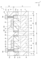
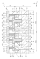
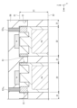
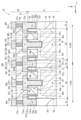
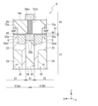
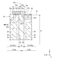
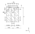
- 5B is an enlarged schematic longitudinal sectional view of a portion of FIG. 5A.
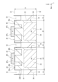
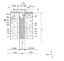
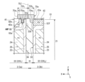
- 4B is a longitudinal sectional view showing a schematic enlarged view of a portion of the longitudinal sectional structure taken along the b4-b4 cutting line in FIG. 4A.
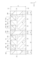
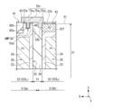
- 4B is a longitudinal sectional view showing a schematic enlarged view of a portion of the longitudinal sectional structure taken along the c4-c4 cutting line in FIG. 4A.
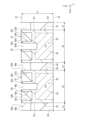
- 4B is a longitudinal sectional view showing a schematic enlarged view of a portion of the longitudinal sectional structure taken along the d4-d4 cutting line in FIG. 4A.
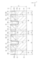
- 4B is a diagram (a longitudinal cross-sectional view taken along the same position as the a4-a4 cutting line in FIG.
- FIG. 10 is a diagram (a vertical cross-sectional view taken along the same position as the a4-a4 cutting line in FIG. 4A) showing a step subsequent to the step in FIG. 9;
- 11 is a diagram (a vertical cross-sectional view taken along the same position as the a4-a4 cutting line in FIG. 4A) showing a step subsequent to the step in FIG. 10;
- FIG. 12 is a diagram (a vertical cross-sectional view taken along the same position as the a4-a4 cutting line in FIG. 4A) showing a process subsequent to FIG. 11.
- FIG. 13 is a diagram (a vertical cross-sectional view taken along the same position as the a4-a4 cutting line in FIG. 4A) showing a process subsequent to FIG. 12.
- 14 is a diagram (a vertical cross-sectional view taken along the same position as the b4-b4 cutting line in FIG. 4A) showing a process subsequent to FIG. 13.
- 15 is a diagram (a vertical cross-sectional view taken along the same position as the b4-b4 cutting line in FIG. 4A) showing a process subsequent to FIG. 14.
- 16 is a diagram (a vertical cross-sectional view taken along the same position as the a4-a4 cutting line in FIG. 4A) showing a process subsequent to FIG. 15.
- 17 is a diagram (a vertical cross-sectional view taken along the same line a4-a4 in FIG. 4A) showing a process subsequent to FIG. 16.
- 17 is a diagram (a vertical cross-sectional view taken along the same position as the b4-b4 cutting line in FIG. 4A) showing a process subsequent to FIG. 16.
- 17B is a diagram (a vertical cross-sectional view taken along the same line a4-a4 in FIG. 4A) showing a process subsequent to FIG. 17A.
- 17B (a longitudinal cross-sectional view taken along the same line b4-b4 in FIG. 4A).
- FIG. 11 is a longitudinal sectional view illustrating a schematic view of a portion of a longitudinal sectional structure of a solid-state imaging device according to a second embodiment of the present technology.
- FIG. 13 is a plan view illustrating a schematic configuration example of one pixel block in a solid-state imaging device according to a third embodiment of the present technology.
- FIG. 20 is a longitudinal sectional view showing a schematic diagram of a portion of the longitudinal sectional structure taken along the a20-a20 cutting line in FIG. 13 is a plan view illustrating a part of a vertical cross-sectional structure of a solid-state imaging device according to a fourth embodiment of the present technology.
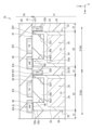
- FIG. 13 is a plan view illustrating a schematic configuration example of two pixel blocks in a solid-state imaging device according to a fifth embodiment of the present technology.
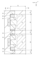
- FIG. 24 is a longitudinal sectional view showing a schematic enlarged view of a portion of the longitudinal sectional structure taken along the a23-a23 cutting line in FIG. 23.
- 13 is a plan view illustrating a schematic configuration example of two pixel blocks in a solid-state imaging device according to a sixth embodiment of the present technology.
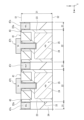
- FIG. 26 is a longitudinal sectional view showing a schematic enlarged view of a portion of the longitudinal sectional structure taken along the a25-a25 cutting line in FIG. 25.
- 26 is a longitudinal sectional view showing a schematic enlarged view of a portion of the longitudinal sectional structure taken along the b25-b25 cutting line in FIG. 25.
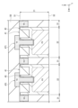
- 26 is a longitudinal sectional view showing a schematic enlarged view of a portion of the longitudinal sectional structure taken along the c25-c25 line in FIG. 25.
- 26 is a longitudinal sectional view showing a schematic enlarged view of a portion of the longitudinal sectional structure taken along the d25-d25 line in FIG. 25.
- 13 is an equivalent circuit diagram showing a configuration example of a pixel and a pixel circuit in a solid-state imaging device according to a seventh embodiment of the present technology.
- FIG. 1 is an equivalent circuit diagram showing a configuration example of a pixel and a pixel circuit in a solid-state imaging device according to a seventh embodiment of the present technology.
- FIG. 34 is a longitudinal sectional view showing a schematic enlarged view of a portion of the longitudinal sectional structure taken along the a34-a34 cutting line in FIG.
- FIG. 23 is a longitudinal cross-sectional view of a main portion that illustrates a modified example 8-1 according to an eighth embodiment of the present technology.
- FIG. 23 is a longitudinal cross-sectional view of a main portion that illustrates a modified example 8-2 according to the eighth embodiment of the present technology.
- FIG. 23 is a longitudinal cross-sectional view of a main portion that illustrates a modified example 8-3 according to the eighth embodiment of the present technology.
- FIG. 23 is a longitudinal cross-sectional view of a main portion that illustrates a modified example 8-4 according to the eighth embodiment of the present technology.
- FIG. 23 is a longitudinal cross-sectional view of a main portion that illustrates a modified example 8-5 according to the eighth embodiment of the present technology.
- FIG. 23 is a longitudinal cross-sectional view of a main portion that illustrates a modified example 8-6 according to the eighth embodiment of the present technology.
- FIG. 23 is a longitudinal cross-sectional view of a main portion that illustrates a modified example 8-7 according to the eighth embodiment of the present technology.
- 13 is a plan view illustrating a schematic configuration example of two pixel blocks in a solid-state imaging device according to a ninth embodiment of the present technology.
- FIG. 44 is a longitudinal sectional view showing a schematic longitudinal sectional structure taken along the a43-a43 cutting line in FIG.
- FIG. 16 is a plan view illustrating a schematic configuration example of two pixel blocks in a solid-state imaging device according to a tenth embodiment of the present technology.
- FIG. 46 is a longitudinal sectional view showing a schematic longitudinal sectional structure taken along the a45-a45 cutting line in FIG. 45.
- FIG. 23 is a diagram showing a configuration example of an electronic device according to an eleventh embodiment of the present technology.
- up and down and other directions in the following explanation are merely for the convenience of explanation and do not limit the technical ideas of this technology. For example, if an object is rotated 90 degrees and observed, up and down are converted into left and right and read, and of course, if it is rotated 180 degrees and observed, up and down are read inverted.
- a first direction and a second direction mutually orthogonal in the same plane are defined as an X direction and a Y direction, respectively, and a third direction perpendicular to each of the first direction and the second direction is defined as a Z direction.
- the thickness direction of a semiconductor layer 21 described later will be described as the Z direction.
- the term "planar view” refers to a view from a direction along the thickness direction of the semiconductor layer 21 described later.
- the term “thickness direction of the semiconductor layer” refers to a direction representing the thickness of the semiconductor layer 21.
- CMOS complementary metal oxide semiconductor
- the solid-state imaging device 1A is mainly composed of a semiconductor chip 2 having a rectangular two-dimensional planar shape when viewed in a plane. That is, the solid-state imaging device 1A is mounted on the semiconductor chip 2, and the semiconductor chip 2 can be regarded as the solid-state imaging device 1A. As shown in Fig. 1, the solid-state imaging device 1A according to the first embodiment of the present technology is mainly composed of a semiconductor chip 2 having a rectangular two-dimensional planar shape when viewed in a plane. That is, the solid-state imaging device 1A is mounted on the semiconductor chip 2, and the semiconductor chip 2 can be regarded as the solid-state imaging device 1A. As shown in Fig.
- this solid-state imaging device 1A (101) takes in image light (incident light 106) from a subject via an optical lens 102, converts the amount of incident light 106 imaged on an imaging surface into an electrical signal on a pixel-by-pixel basis, and outputs the electrical signal as a pixel signal.
- the semiconductor chip 2 on which the solid-state imaging device 1A is mounted has, in a two-dimensional plane including mutually orthogonal X and Y directions, a square pixel array section 2A provided in the center, and a peripheral section 2B provided outside the pixel array section 2A so as to surround the pixel array section 2A.
- the semiconductor chip 2 is formed by dicing a semiconductor wafer including a semiconductor layer 21 described below into chip formation regions. Therefore, the configuration of the solid-state imaging device 1A described below is generally the same in the wafer state before the semiconductor wafer is diced. In other words, this technology can be applied in the state of a semiconductor chip and in the state of a semiconductor wafer.
- the pixel array section 2A is a light receiving surface that receives light collected by, for example, an optical lens (optical system) 102 shown in FIG. 47.
- a plurality of pixels 3 (sensor pixels) are arranged in a matrix on a two-dimensional plane including the X direction and the Y direction.
- the pixels 3 are repeatedly arranged in each of the X direction and the Y direction that are mutually orthogonal within the two-dimensional plane.
- a plurality of bonding pads 14 are arranged in the peripheral portion 2B.
- Each of the plurality of bonding pads 14 is arranged, for example, along each of the four sides of the semiconductor chip 2 in a two-dimensional plane.
- Each of the plurality of bonding pads 14 functions as an input/output terminal that electrically connects the semiconductor chip 2 to an external device.
- the semiconductor chip 2 includes a logic circuit 13 shown in Fig. 2.
- the logic circuit 13 includes a vertical drive circuit 4, a column signal processing circuit 5, a horizontal drive circuit 6, an output circuit 7, and a control circuit 8.
- the logic circuit 13 is configured of a CMOS (Complementary MOS) circuit having, as field effect transistors, for example, n-channel conductivity type MOSFETs (Metal Oxide Semiconductor Field Effect Transistors) and p-channel conductivity type MOSFETs.
- CMOS Complementary MOS
- the vertical drive circuit 4 shown in FIG. 2 is composed of, for example, a shift register.
- the vertical drive circuit 4 sequentially selects the desired pixel drive lines 10, supplies pulses to the selected pixel drive lines 10 for driving the pixels 3, and drives each pixel 3 row by row. That is, the vertical drive circuit 4 sequentially selects and scans each pixel 3 in the pixel array section 2A vertically row by row, and supplies pixel signals from the pixels 3 based on signal charges generated by the photoelectric conversion section of each pixel 3 according to the amount of light received to the column signal processing circuit 5 via the vertical signal line 11.
- the column signal processing circuit 5 shown in FIG. 2 is arranged, for example, for each column of pixels 3, and performs signal processing such as noise removal for each pixel column on signals output from one row of pixels 3.
- the column signal processing circuit 5 performs signal processing such as CDS (Correlated Double Sampling) and AD (Analog-to-Digital) conversion to remove pixel-specific fixed pattern noise.
- the horizontal drive circuit 6 shown in FIG. 2 is composed of, for example, a shift register.
- the horizontal drive circuit 6 sequentially outputs horizontal scanning pulses to the column signal processing circuits 5, thereby selecting each of the column signal processing circuits 5 in turn, and causing each of the column signal processing circuits 5 to output a pixel signal that has been subjected to signal processing to the horizontal signal line 12.
- the output circuit 7 shown in FIG. 2 processes and outputs pixel signals sequentially supplied from each of the column signal processing circuits 5 through the horizontal signal line 12.
- the signal processing may include buffering, black level adjustment, column variation correction, various types of digital signal processing, etc.
- the control circuit 8 shown in FIG. 2 generates clock signals and control signals that serve as the basis for the operation of the vertical drive circuit 4, column signal processing circuit 5, horizontal drive circuit 6, etc., based on the vertical synchronization signal, horizontal synchronization signal, and master clock signal. The control circuit 8 then outputs the generated clock signals and control signals to the vertical drive circuit 4, column signal processing circuit 5, horizontal drive circuit 6, etc.
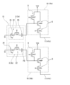
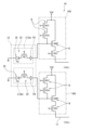
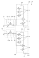
- the semiconductor chip 2 includes a pixel block 15 and a pixel circuit (readout circuit) 16 shown in FIG.
- the pixel block 15 includes a plurality of pixels 3.
- the pixel block 15 of the first embodiment includes, for example, two pixels 3 (3a, 3b) arranged adjacent to each other in the X direction in a plan view as one unit, although this is not limited thereto.
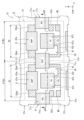
- Fig. 3 mainly illustrates one pixel block 15, and
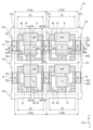
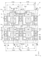
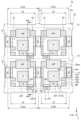
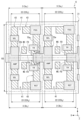
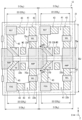
- Fig. 4A mainly illustrates two pixel blocks 15 arranged adjacent to each other in the Y direction, but the pixel blocks 15 are repeatedly arranged in each of the X direction and the Y direction to form the pixel array unit 2A shown in Fig. 1.
- the semiconductor chip 2 further includes a multi-layer wiring layer 55 provided on the first surface S1 side of the semiconductor layer 21.
- the semiconductor chip 2 further includes a planarization film 61, an optical filter 63, and a microlens (on-chip lens) 64 provided in this order from the second surface S2 side of the semiconductor layer 21.
- the p-type semiconductor region 23 is provided over a wide area in the photoelectric conversion region 22, extending across the first surface portion S1 side and the second surface portion S2 side of the semiconductor layer 21.
- the p-type semiconductor region 23 contacts the inter-pixel isolation region 31 along the depth direction (Z direction) of the semiconductor layer 21.
- the floating diffusion region FD is provided in the p-type semiconductor region 23 on the first surface portion S1 side of the semiconductor layer 21 (the upper surface portion 22a side of the photoelectric conversion region 22).
- the floating diffusion region FD overlaps with the n-type semiconductor region 24 in a plan view, and is separated from the n-type semiconductor region 24 in the thickness direction (Z direction) of the semiconductor layer 21. That is, the p-type semiconductor region 23 is provided between the floating diffusion region FD and the n-type semiconductor region 24.
- the floating diffusion region FD also serves as a main electrode region 52r of the reset transistor RST described later, and is composed of an n-type semiconductor region.
- the element isolation region 41 is provided in a surface layer portion on the upper surface portion 22a side of the photoelectric conversion region 22, i.e., a surface layer portion on the first surface portion S1 side of the semiconductor layer 21.
- the element isolation region 41 has, but is not limited to, an STI (Shallow Trench Isolation) structure in which an isolation insulating film 42b is embedded inside a shallow groove portion 42a recessed from the first surface portion S1 to the second surface portion S2 side of the semiconductor layer 21, for example.
- STI Shallow Trench Isolation
- the inter-element isolation region 41 has an island-like planar pattern that is separated from the inter-pixel isolation region 31 except for a portion when viewed from above, and defines the element formation region 43 together with the inter-pixel isolation region 31.
- the element formation region 43 is provided in the surface layer on the upper surface 22a side of the photoelectric conversion region 22, i.e., the surface layer on the first surface S1 side of the semiconductor layer 21.
- the element formation region 43 is partitioned by the inter-element isolation region 41 and the inter-pixel isolation region 31, and has a planar pattern extending in a ribbon shape along the four sides of the photoelectric conversion region 22 in a planar view.
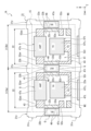
- the planar pattern of the element formation region 43 is different for the two pixels 3a, 3b included in the pixel block 15. That is, as shown in FIG. 4B, for the two pixels 3a, 3b included in the pixel block 15, the planar pattern of the element formation region 43 in one pixel 3a and the planar pattern of the element formation region 43 in the other pixel 3b are inverted about the boundary between the pixels 3a and 3b aligned in the X direction.
- the p-type power supply contact region WC is provided on the corner side between two sides of the photoelectric conversion region 22 in a plan view.
- the p-type power supply contact region WC is provided on the surface layer portion on the upper surface portion 22a side of the photoelectric conversion region 22, i.e., the surface layer portion on the first surface portion S1 side of the semiconductor layer 21.
- the p-type power supply contact region WC is provided in an island-shaped power supply region partitioned by the inter-element isolation region 41 and the inter-pixel isolation region 31 on the upper surface portion 22a side of the photoelectric conversion region 22.
- a first reference potential of, for example, 0 V is applied to this p-type power supply contact region WC during operation as a reference potential within the semiconductor chip 2 (within the solid-state imaging device 1A), and the potential is fixed to this first reference potential.
- the transfer transistor TR is provided on the first surface S1 side of the semiconductor layer 21, that is, on the upper surface 22a side of the photoelectric conversion region 22.
- the transfer transistor TR has a gate electrode 47t provided on the upper surface 22a side of the photoelectric conversion region 22 across the inside and outside of the photoelectric conversion region 22, and a gate insulating film 46 provided between the gate electrode 47t and the semiconductor layer 21.
- the transfer transistor TR further has an n-type semiconductor region 24 functioning as a source region, an n-type floating diffusion region FD functioning as a drain region, and a p-type semiconductor region 23 functioning as a channel formation portion.
- the transfer transistor TR is, for example, configured as a vertical type, but is not limited thereto.
- the gate electrode 47t of the transfer transistor TR has a head 47t1 provided on the outside of the first surface portion S1 of the semiconductor layer 21 with the gate insulating film 46 interposed therebetween, and a leg 47r2 protruding from the head 47t1 into the semiconductor layer 21 and adjacent to the semiconductor layer 21 with the gate insulating film 46 interposed therebetween.
- the gate electrode 47t of the first embodiment is configured, for example, to have a T-shaped vertical cross section in which the width of the leg 47t2 is narrower than the width of the head 47t1 , although this is not limited thereto.
- a leg portion 47t2 of the gate electrode 47t is provided in the recessed portion 45a of the semiconductor layer 21 with the gate insulating film 46 interposed therebetween, and the tip of the leg portion 47t2 extends into the n-type semiconductor region 24 with being insulated and isolated.
- a plurality of pixel transistors Q (AMP, SEL, RST) included in the pixel circuit 16 are provided in the element formation region 43. At least one of the plurality of pixel transistors Q has a gate electrode provided in the inter-pixel isolation region 31.
- the gate electrodes 47s and 47r of the selection transistor SEL and the reset transistor RST are provided in the inter-pixel isolation region 31.
- the amplifier transistor AMP has a gate electrode 47a provided on the upper surface portion 22a side of the photoelectric conversion region 22 (the first surface portion S1 side of the semiconductor layer 21) so as to overlap with the element formation region 43 (semiconductor layer 21) in a planar view, and a gate insulating film 46 interposed between the gate electrode 47a and the element formation region 43.
- the amplifier transistor AMP further has a pair of main electrode regions 52as and 52ar provided in the element formation region 43 on both sides in the gate length direction of the gate electrode 47a and functioning as a source region and a drain region.
- the amplifier transistor AMP further has a channel formation portion 53a (see FIG.
- the pair of main electrode regions 52as and 52ar are separated from each other via the channel formation portion 53a.
- the pair of main electrode regions 52 as and 52 ar are formed of n-type semiconductor regions provided in the element formation region 43
- the channel formation portion 53 a is formed of a p-type semiconductor region 23 provided in the element formation region 43 .
- the reset transistor RST is provided on the inter-pixel isolation region 31 side between two photoelectric conversion regions 22 included in the pixel block 15.
- the reset transistor RST has a gate electrode 47r provided in the inter-pixel isolation region 31 adjacent to each other with the first side portion 22b of the photoelectric conversion region 22 and the gate insulating film 46 interposed therebetween, and a pair of main electrode regions 52r and 52ar provided on the upper surface portion 22a of the photoelectric conversion region 22 spaced apart from each other in the gate length direction of the gate electrode 47r in a plan view and functioning as a source region and a drain region.
- the reset transistor RST further has a channel formation portion 53r provided in the element formation region 43 (semiconductor layer 21) adjacent to the gate electrode 47r in a plan view.
- the pair of main electrode regions 52r and 52ar are formed of n-type semiconductor regions, and the channel formation portion 53r is formed of a p-type semiconductor region 23.
- the gate electrode 47r of the reset transistor RST is not limited to this first embodiment, but may be selectively provided in the inter-pixel isolation region 31 and embedded in the inter-pixel isolation region 31, for example.
- the reset transistor RST and the amplifying transistor AMP share the main electrode region 52as of the reset transistor RST and the main electrode region 52as of the amplifying transistor AMP, and are provided in series connection in the element formation region 43.
- the reset transistor RST has a pair of main electrode regions 52r and 52ar, of which one main electrode region 52r is also used as the floating diffusion region FD.
- the reset transistor RST is shared by two pixels 3a and 3b (two photoelectric conversion regions 22) included in the pixel block 15.
- the gate electrode 47r of the reset transistor RST is adjacent to the first side portion 22b of each of the two photoelectric conversion regions 22 adjacent to each other in a planar view, with the gate insulating film 46 interposed between them. That is, the reset transistor RST of this first embodiment has a gate electrode 47r provided in the inter-pixel isolation region 31 between the two photoelectric conversion regions 22 adjacent to each other in a planar view, and a pair of main electrode regions 52r, 52ar and a channel formation portion 53r provided in each of the two photoelectric conversion regions 22 adjacent to each other in a planar view.
- the selection transistor SEL is provided on the opposite side of the photoelectric conversion region 22 from the reset transistor TST side in a plan view.
- the selection transistor SEL has a gate electrode 47s provided in the inter-pixel isolation region 31 adjacent to the first side portion 22b of the photoelectric conversion region 22 with the gate insulating film 46 interposed therebetween, and a pair of main electrode regions 52s and 52as provided on the upper surface portion 22a of the photoelectric conversion region 22 spaced apart from each other in the gate length direction of the gate electrode 47s in a plan view and functioning as a source region and a drain region.
- the selection transistor SEL further has a channel formation portion 53s provided in the element formation region 43 (semiconductor layer 21) adjacent to the gate electrode 47s in a plan view.
- the pair of main electrode regions 52s and 52as are formed of n-type semiconductor regions, and the channel formation portion 53s is formed of a p-type semiconductor region 23.
- the gate electrode 47s of the selection transistor SEL is not limited to this first embodiment, but may be selectively provided in the inter-pixel isolation region 31 and embedded in the inter-pixel isolation region 31, for example.
- the selection transistor SEL and the amplification transistor AMP share the main electrode region 52as of the selection transistor SEL and the main electrode region 52as of the amplification transistor AMP, and are provided in the element formation region 43 in a series connection.
- the selection transistor SEL in two pixel blocks 15 aligned in the X direction, the selection transistor SEL is shared by the pixel 3a of one pixel block 15 and the pixel 3b of the other pixel block 15.
- the selection transistor SEL in the two pixel blocks 15 aligned in the X direction, the selection transistor SEL is shared by the pixel circuit 16a assigned to the pixel 3a of one pixel block 15 and the pixel circuit 16b assigned to the pixel 3b of the other pixel block 15.
- the select transistor SEL has a gate electrode 47s adjacent to each of the first side portions 22b of the two photoelectric conversion regions 22 adjacent to each other in a planar view, with the gate insulating film 46 interposed therebetween.
- the select transistor SEL of the first embodiment has a gate electrode 47s provided in an inter-pixel isolation region 31 between the two photoelectric conversion regions 22 adjacent to each other in a planar view, and a pair of main electrode regions 52s, 52as and a channel formation portion 53s provided in each of the two photoelectric conversion regions 22 adjacent to each other in a planar view.
- the channel formation portions 53r, 53s of the reset transistor RST and the select transistor SEL are formed of the semiconductor layer 21 between the first side portion 22b and the second side portion 22c of the photoelectric conversion region 22. That is, the reset transistor TRS and the select transistor SEL each have the channel formation portions 53r, 53s between the first side portion 22b and the second side portion 22c of the photoelectric conversion region 22. In other words, the reset transistor RST and the select transistor SEL each have the channel formation portions 53r, 53s in the semiconductor layer 21 between the pixel isolation region 31 and the device isolation region 41.
- the thickness of the channel formation portions 53r, 53s in a plan view can be reduced by reducing the distance between the pixel isolation region 31 and the device isolation region 41.
- the thickness of the channel formation portions 53r, 53s is preferably less than 100 nm.
- the gate electrodes 47a, 47s, 47r, and 47t of the amplification transistor AMP, the selection transistor SEL, the reset transistor RST, and the transfer transistor TR are each made of, for example, a polycrystalline silicon film (doped polysilicon film) doped with an impurity that reduces the resistance value.
- Each of the reset transistor RST and the selection transistor SEL can be configured as an enhancement type (normally off type) in which a drain current flows by applying a gate voltage equal to or higher than a threshold voltage to the gate electrodes 47r and 47s. Also, each of the reset transistor RST and the selection transistor SEL can be configured as a depression type (normally on type) in which a drain current flows even if no voltage is applied to the gate electrodes 47r and 47s. In this first embodiment, the transistors are configured as, for example, an enhancement type, although this is not limited thereto.
- a channel (inversion layer) electrically connecting a pair of main electrode regions 52r (52s) and 52ar (52as) is formed (induced) in the channel formation portions 53r and 53s by a voltage applied to the gate electrodes 47r and 47s, and a current (drain current) flows from the drain region side (e.g., the main electrode region 52r, 52s side) through the channel of the channel formation portions 53r and 53s to the source region side (e.g., the main electrode region 52ar, 52as side).
- the amplification transistor AMP is also configured as, for example, an enhancement type.
- the photoelectric conversion region 22 has a first side portion 22b on the inter-pixel isolation region 31 side and a second side portion 22c located on the opposite side to the first side portion 22b and adjacent to the inter-element isolation region 41.
- the reset transistor RST and the select transistor SEL each have a channel formation portion 53r, 53s between the first side portion 22b and the second side portion 22c of the photoelectric conversion region 22. Therefore, the thickness of the channel formation portion 53r, 53s in the planar direction can be easily adjusted by the distance between the inter-pixel isolation region 31 and the inter-element isolation region 41, and the channel formation portion 53r, 53s can be thinned (thinned).
- the inter-pixel isolation region 31 of the first embodiment described above is composed of one vertical portion that extends linearly across the first surface portion S1 side and the second surface portion S2 side of the semiconductor layer 21.
- the gate electrodes 47r, 47s of the reset transistor RST and the selection transistor SEL are embedded in the first vertical portion 31b1 of the inter-pixel isolation region 31B.
- the gate electrodes 47r, 47s are adjacent to the first side portion 22b of the photoelectric conversion region 22 with the gate insulating film 46 interposed therebetween.
- the solid-state imaging device 1C of the third embodiment of the present technology is basically configured in the same manner as the solid-state imaging device 1A of the first embodiment described above, except for the configurations of the gate electrodes of the reset transistor RST and the selection transistor SEL.
- the reset transistor RST and the select transistor SEL of this third embodiment have gate electrodes 71r and 71s instead of the gate electrodes 47r and 47s shown in Figures 4B and 5B of the first embodiment described above.
- the other configurations are generally similar to those of the first embodiment.
- the gate electrode 71r of the reset transistor RST is provided across the upper surface portion 22a and the first side surface portion 22b of the photoelectric conversion region 22, with the gate insulating film 46 interposed therebetween.
- the gate electrode 71r has a head 71r1 extending across the photoelectric conversion region 22 and the inter-pixel isolation region 31 in a plan view outside the first surface portion S1 of the semiconductor layer 21, and a leg portion 71r2 protruding from the head 71r1 toward the inter-pixel isolation region 31 and adjacent to the first side surface portion 22b of the photoelectric conversion region 22 with the gate insulating film 46 interposed therebetween.
- the gate insulating film 46 is provided between the head 71r1 and an upper surface portion 22a of the photoelectric conversion region 22.
- the gate electrode 71s of the selection transistor SEL is also provided across the upper surface portion 22a and the first side surface portion 22b of the photoelectric conversion region 22 with the gate insulating film 46 interposed therebetween.
- the gate electrode 71s has a head 71s1 extending across the photoelectric conversion region 22 and the inter-pixel isolation region 31 in a plan view outside the first surface portion S1 of the semiconductor layer 21 , and a leg portion 71s2 protruding from the head 71s1 toward the inter-pixel isolation region 31 and adjacent to the first side surface portion 22b of the photoelectric conversion region 22 with the gate insulating film 46 interposed therebetween.
- the gate insulating film 46 is also provided between the head 71s1 and an upper surface portion 22a of the photoelectric conversion region 22.
- the solid-state imaging device 1C according to the third embodiment also provides the same effects as the solid-state imaging device 1A according to the first embodiment described above.
- the gate electrodes 71r, 71s of the reset transistor RST and the select transistor SEL in the third embodiment are provided across the upper surface portion 22a and the first side surface portion 22b of the photoelectric conversion region 22 with the gate insulating film 46 interposed therebetween, so that the gate width Wg of the gate electrodes 71r, 71s can be made wider than in the first embodiment.
- the solid-state imaging device 1D of the fourth embodiment of the present technology is basically configured in the same manner as the solid-state imaging device 1A of the first embodiment described above, except for the configurations of the gate electrodes of the reset transistor RST and the selection transistor SEL.
- the reset transistor RST and the select transistor SEL of the fourth embodiment have gate electrodes 72r and 72s instead of the gate electrodes 47r and 47s shown in FIG. 4B and FIG. 5B of the first embodiment described above.
- the other configurations are generally similar to those of the first embodiment.
- the gate electrode 72r of the reset transistor RST is provided across the upper surface portion 22a, the first side surface portion 22b, and the second side surface portion 22c of the photoelectric conversion region 22, with the gate insulating film 46 interposed therebetween.
- the gate electrode 72r has a head 72r1 located outside the first surface portion S1 of the semiconductor layer 21 and extending across the inter-pixel isolation region 31 and the inter-element isolation region 41 across the upper surface portion 22a (element formation region 43) of the photoelectric conversion region 22 in a plan view, a first leg portion 72r2 protruding from the head 72r1 toward the inter-pixel isolation region 31 and adjacent to the first side surface portion 22b of the photoelectric conversion region 22 with the gate insulating film 46 interposed therebetween, and a second leg portion 72r3 protruding from the head 72r1 toward the inter-element isolation region 41 and adjacent to the second side surface portion 22c of the photoelectric conversion region 22 with the gate insulating film 46 interposed therebetween.
- the gate insulating film 46 is provided between the head 72r1 and the upper surface portion 22a of the photoelectric conversion region 22. Also in the fourth embodiment, the reset transistor RST is shared by two pixels 3a and 3b arranged adjacent to each other in the X direction, so that the gate electrode 72r has one head portion 72r1 and two second leg portions 72r3 .
- the gate electrode 72s of the select transistor SEL is provided across the upper surface portion 22a, the first side surface portion 22b, and the second side surface portion 22c of the photoelectric conversion region 22 with the gate insulating film 46 interposed therebetween.
- the gate electrode 72s has a head 72s1 that is provided outside the first surface portion S1 of the semiconductor layer 21 and extends across the inter-pixel isolation region 31 and the inter-element isolation region 41 across the upper surface portion 22a of the photoelectric conversion region 22 in a plan view, a first leg 72s2 that protrudes from the head 72s1 toward the inter-pixel isolation region 31 and is adjacent to the first side surface portion 22b of the photoelectric conversion region 22 with the gate insulating film 46 interposed therebetween, and a second leg 72r3 that protrudes from the head 72sr1 toward the inter-element isolation region 41 and is adjacent to the second side surface portion 22c of the photoelectric conversion region 22 with the gate insulating film 46 interposed therebetween.
- the gate insulating film 46 is provided between the head 72r1 and the upper surface portion 22a of the photoelectric conversion region 22. Also in this fourth embodiment, in two pixel blocks 15 arranged adjacent to each other in the X direction, the pixel 3 b of one pixel block 15 and the pixel 3 a of the other pixel block 15 share the selection transistor SEL, and therefore the gate electrode 72 s also has one head 72 s 1 and two second leg portions 72 s 3 .
- the solid-state imaging device 1D according to the fourth embodiment also provides the same effects as the solid-state imaging device 1A according to the first embodiment described above.
- the gate electrodes 72r, 72s of the reset transistor RST and the select transistor SEL in this fourth embodiment are provided across the upper surface portion 22a, the first side surface portion 22b, and the second side surface portion 22c of the photoelectric conversion region 22 with the gate insulating film 46 interposed therebetween, so that the gate width Wg of the gate electrodes 72r, 72s can be made wider than in the third embodiment.
- the solid-state imaging device 1E of the fifth embodiment of the present technology is basically configured in the same manner as the solid-state imaging device 1A of the first embodiment described above, except for the configuration of the amplification transistor AMP.
- the amplification transistor AMP of the fifth embodiment has a gate electrode 47a provided in the inter-pixel isolation region 31 between two photoelectric conversion regions 22 adjacent to each other in the Y direction in a plan view.
- the amplification transistor AMP of the fifth embodiment has a gate electrode 47a provided in the inter-pixel isolation region 31 adjacent to the first side portion 22b of the photoelectric conversion region 22 with the gate insulating film 46 interposed therebetween, and a pair of main electrode regions 52as and 52ar provided on the upper surface portion 22a of the photoelectric conversion region 22 spaced apart from each other in the gate length direction of the gate electrode 47a in a plan view, and functioning as a source region and a drain region.
- the amplification transistor AMP further has a channel formation portion 53a provided in the element formation region 43 (semiconductor layer 21) adjacent to the gate electrode 47a in a plan view.
- the pair of main electrode regions 52as and 52ar are formed of n-type semiconductor regions, and the channel formation portion 53r is formed of a p-type semiconductor region 23.
- the solid-state imaging device 1E according to the fifth embodiment also provides the same effects as the solid-state imaging device 1A according to the first embodiment described above.
- the gate electrode 47a is connected to the floating diffusion region FD so as to be adjacent to each other in a plan view. This allows the gate electrode 47a and the floating diffusion region FD to be electrically connected over the shortest distance, and reduces the wiring capacitance added to the floating diffusion region FD compared to when the gate electrode 47a and the floating diffusion region FD are electrically connected via wiring in the multilayer wiring layer 55. This allows the conversion efficiency to be increased and random noise to be reduced.
- the solid-state imaging device 1F according to the sixth embodiment of the present technology has a configuration basically similar to that of the solid-state imaging device 1A according to the first embodiment described above, but differs in the configuration of the amplifying transistor AMP.
- the solid-state imaging device 1F according to the sixth embodiment of the present technology further includes relay conductor parts 74a and 74b provided in the inter-pixel isolation region 31.
- the amplification transistor AMP of the sixth embodiment includes a gate electrode 73a instead of the gate electrode 47a of the first embodiment shown in Fig. 4A and 7.
- the other configurations are generally similar to those of the first embodiment.
- the amplification transistor AMP provided in one of the photoelectric conversion regions 22 has a gate electrode 73a that is provided across the upper surface portion 22a of one of the photoelectric conversion regions 22 and the inter-pixel isolation region 31 in a plan view, and is electrically and mechanically connected to the floating diffusion region FD provided in the other photoelectric conversion region 22 at the first side portion 22b of the other photoelectric conversion region 22.
- the gate electrode 73a of the amplification transistor AMP has a head 73a1 extending across one photoelectric conversion region 22 and the inter-pixel isolation region 31 in a plan view outside the first surface portion S1 of the semiconductor layer 21, and a relay protrusion 73a3 protruding from the head 73a1 toward the inter-pixel isolation region 31 and electrically and mechanically connected to the floating diffusion region FD of the other photoelectric conversion region 22 at the first side surface portion 22b of the other photoelectric conversion region 22.
- a gate insulating film 46 is interposed between the head 73a1 and the upper surface portion 22a of the one photoelectric conversion region 22.
- the relay protrusion 73a3 is embedded in the inter-pixel isolation region 31.
- the relay conductor 74a is provided in the inter-pixel separation region 31 between two photoelectric conversion regions 22 included in one pixel block 15.
- the relay conductor 74a is electrically and mechanically connected to the main electrode region 52ar of the amplifier transistor AMP in one of the two photoelectric conversion regions 22 included in one pixel block 15 at the first side surface portion 22b of one of the photoelectric conversion regions 22, and is also electrically and mechanically connected to the main electrode region 52ar of the amplifier transistor AMP in the other photoelectric conversion region 22 at the first side surface portion 22b of the other photoelectric conversion region 22.
- the relay conductor 74a is electrically and mechanically connected to the main electrode region 52ar of each of the two amplifier transistors AMP adjacent to each other across the inter-pixel separation region 31 at the first side surface portion 22b of each of the two photoelectric conversion regions 22 adjacent to each other in a plan view.
- the relay conductor portion 74a is embedded in the inter-pixel isolation region 31, penetrates the inter-pixel isolation region 31 in the X direction, and is connected to the first side portion 22b of each of the two photoelectric conversion regions 22 included in one pixel block 15.
- the relay conductor portion 74a is electrically connected to the wiring 58ar provided in the wiring layer 58 on the inter-layer insulating film 56 via the contact electrode 57ar provided in the inter-layer insulating film 56.
- the relay conductor 74b is provided in the inter-pixel separation region 31 between two pixel blocks 15 arranged adjacent to each other in the X direction.
- the relay conductor 74b is electrically and mechanically connected to the power supply contact region WC of one photoelectric conversion region 22 at the first side portion 22b of one photoelectric conversion region 22 in two adjacent photoelectric conversion regions 22 in the two pixel blocks 15 arranged in the X direction, and is electrically and mechanically connected to the power supply contact region WC of the other photoelectric conversion region 22 at the first side portion 22b of the other photoelectric conversion region 22.
- the relay conductor 74b is electrically and mechanically connected to two power supply contact regions WC adjacent to each other across the inter-pixel separation region 31 at the first side portion 22b of each of the two photoelectric conversion regions 22 adjacent to each other in a plan view.
- the relay conductor portion 74b is not shown in detail, but referring to FIG. 28, it is embedded in the inter-pixel isolation region 31, like the relay conductor portion 74a, and penetrates the inter-pixel isolation region 31 in the X direction, and is connected to the first side portion 22b of each of the two photoelectric conversion regions 22 adjacent to each other with the inter-pixel isolation region 31 in between. And, like the relay conductor portion 74a, the relay conductor portion 74b is electrically connected to the wiring 58wc provided in the wiring layer 58 on the inter-layer insulating film 56 via the contact electrode 57wc provided in the inter-layer insulating film 56. A reference potential of, for example, 0V is supplied from the wiring 58wc through the contact electrode 57wc to the relay conductor portion 74b.
- Each of the relay conductors 74a and 74b is made of, for example, a polycrystalline silicon film into which an impurity that reduces the resistance value has been introduced. Although a metal film may be used for each of the relay conductors 74a and 74b, it is preferable to use a polycrystalline silicon film in consideration of the difference in thermal expansion coefficient between the inter-pixel isolation region 31 and the semiconductor layer 21.
- the amplification transistor AMP of the sixth embodiment has a gate electrode 73a that is provided across the upper surface portion 22a and the inter-pixel isolation region 31 of one of the two photoelectric conversion regions 22 arranged in the Y direction via the inter-pixel isolation region 31 in a plan view, and is electrically and mechanically connected to the floating diffusion region FD of the other photoelectric conversion region 22 at the first side portion 22b of the other photoelectric conversion region 22.
- the gate electrode 73a of the amplification transistor AMP it is not necessary to electrically connect the gate electrode 73a of the amplification transistor AMP to the floating diffusion region FD by wiring of the multi-layer wiring layer 55, and the wiring density of the multi-layer wiring layer 55 that overlaps with the photoelectric conversion region 22 in a plan view can be reduced.
- This can increase the degree of freedom in routing the wiring that connects to the pixel transistor Q of the photoelectric conversion region 22, and can ease the constraints on the arrangement of the pixel transistor Q caused by the wiring. Therefore, according to the solid-state imaging device 1F of the sixth embodiment, the degree of freedom in the arrangement of the pixel transistor Q in the photoelectric conversion region 22 can be increased.
- the solid-state imaging device 1F also includes a relay conductor 74a provided in the inter-pixel separation region 31 between two photoelectric conversion regions 22 arranged in the X direction of one pixel block 15.
- the relay conductor 74a is electrically and mechanically connected to the main electrode region 52ar of the amplifier transistor AMP in one of the two photoelectric conversion regions 22 included in one pixel block 15 at the first side portion 22b of one photoelectric conversion region 22, and is electrically and mechanically connected to the main electrode region 52ar of the amplifier transistor AMP in the other photoelectric conversion region 22 at the first side portion 22b of the other photoelectric conversion region 22.
- the solid-state imaging device 1F also includes a relay conductor 74b provided in the inter-pixel separation region 31 between two pixel blocks 15 arranged adjacent to each other in the X direction.
- the relay conductor 74b is electrically and mechanically connected to the power supply contact region WC of one photoelectric conversion region 22 at the first side portion 22b of one photoelectric conversion region 22 in two adjacent photoelectric conversion regions 22 in two pixel blocks 15 arranged in the X direction, and is electrically and mechanically connected to the power supply contact region WC of the other photoelectric conversion region 22 at the first side portion 22b of the other photoelectric conversion region 22.
- the solid-state imaging device 1G of the seventh embodiment of the present technology is basically configured in the same manner as the solid-state imaging device 1A of the first embodiment described above, with the following differences in configuration.
- the solid-state imaging device 1G of the seventh embodiment has a pixel circuit 16G shown in FIG. 30 instead of the pixel circuit 16 shown in FIG. 3 of the first embodiment described above.
- the transistor layout of the photoelectric conversion region 22 is slightly different from that of the first embodiment described above.
- the other configurations are generally similar to those of the first embodiment.
- pixel circuit 16G has a circuit configuration in which a switching transistor FDG is newly added to the configuration of pixel circuit 16 described above. That is, pixel circuit 16G includes an amplification transistor AMP, a selection transistor SEL, a reset transistor RST, and a switching transistor FDG as a pixel transistor Q.
- the source region of the switching transistor FDG is electrically connected to the gate electrode and floating diffusion region FD of the amplification transistor AMP, and the drain region is electrically connected to the source region of the reset transistor RST.
- the gate electrode of the switching transistor FDG is electrically connected to the switching transistor drive line of the pixel drive line 10 shown in FIG. 2. This switching transistor FDG controls charge retention by the floating diffusion region FD, and adjusts the voltage multiplication factor according to the potential amplified by the amplification transistor AMP.
- the switching transistor FDG has a gate electrode 47f provided in the inter-pixel isolation region 31 between two photoelectric conversion regions 22 adjacent to each other in the Y direction in plan view.
- the switching transistor FDG has a gate electrode 47f provided in the inter-pixel isolation region 31 adjacent to the first side portion 22b of the photoelectric conversion region 22 with the gate insulating film 46 interposed therebetween, and a pair of main electrode regions 52f and 52r provided on the upper surface portion 22a of the photoelectric conversion region 22 spaced apart from each other in the gate length direction of the gate electrode 47f in a plan view and functioning as a source region and a drain region.
- the switching transistor FDG further has a channel formation portion 53f provided in the element formation region 43 (semiconductor layer 21) adjacent to the gate electrode 47f in a plan view.
- the pair of main electrode regions 52f and 52r are formed of n-type semiconductor regions, and the channel formation portion 53f is formed of a p-type semiconductor region 23.
- the switching transistor FDG is used to switch the conversion efficiency.
- the FD capacitance C of the floating diffusion region FD needs to be large so that the voltage V when converted to a voltage by the amplifier transistor AMP does not become too large (in other words, to become small).
- the switching transistor FDG when the switching transistor FDG is turned on, the gate capacitance of the switching transistor FDG increases, so the overall FD capacitance C becomes large.
- the switching transistor FDG when the switching transistor FDG is turned off, the overall FD capacitance C becomes small. In this way, by switching the switching transistor FDG on and off, the FD capacitance C can be made variable and the conversion efficiency can be changed.
- the floating diffusion region FD is also used as the main electrode region 52f of the switching transistor FDG.
- the reset transistor RST and the switching transistor FDG share the main electrode region 52r of the reset transistor RST and the main electrode region 52r of the switching transistor FDG, and are connected in series.
- the solid-state imaging device 1G according to the seventh embodiment also provides the same effects as the solid-state imaging device 1A according to the first embodiment described above.
- the gate electrodes 47f, 47r, and 47s of the switching transistor FDG, reset transistor RST, and selection transistor SEL are provided in the inter-pixel isolation region 31 as the pixel transistors Q included in the pixel circuit 16G.
- the gate electrode of at least one of the pixel transistors Q included in the pixel circuit 16G may be provided in the inter-pixel isolation region 31.
- the solid-state imaging device 1H of the eighth embodiment of the present technology is basically configured in the same manner as the solid-state imaging device 1A of the first embodiment described above, with the following differences in configuration.
- FIG. 41 is a longitudinal cross-sectional view of a main portion that is a schematic diagram illustrating a modified example 8-6 according to the eighth embodiment of the present technology.
- This modification is a combination of the impurity concentration distribution technique of the modification 8-1 shown in Fig. 36 and the channel width widening technique of the modification 8-3 shown in Fig. 38.
- This modification 8-6 can obtain the effects of each of the above-mentioned modifications 8-1 and 8-3.
- the parasitic capacitance adding technique of variant 8-2 shown in FIG. 37 can be combined with the channel width widening technique of variant 8-3 shown in FIG. 38 and the floating diffusion region connection technique of variant 8-4 shown in FIG. 39.
- a solid-state imaging device 1I according to a ninth embodiment of the present technology includes a pixel block 15I shown in Fig. 43.
- the pixel block 15I according to the ninth embodiment mainly includes two pixels 3 ( 3a1 , 3b1 ) arranged adjacent to each other in the Y direction as one unit.
- Each of the two pixels 3 ( 3a1 , 3b1 ) included in one pixel block 15I includes a photoelectric conversion region 22 ( 22X3 , 22X4 ) partitioned by an inter-pixel isolation region 31.
- the photoelectric conversion region 22 ( 22X3 , 22X4 ) of the ninth embodiment is basically configured similarly to the photoelectric conversion region 22 of the eighth embodiment described above, with the following differences.
- the photoelectric conversion regions 22 ( 22X3 , 22X4 ) of the ninth embodiment are different from the photoelectric conversion region 22 of the eighth embodiment in the transistor layout and the planar shape of the element formation region 43.
- the planar pattern of the element formation region 43 in one photoelectric conversion region 22X3 and the planar pattern of the element formation region 43 in the other photoelectric conversion region 22X4 are inverted about the boundary between pixels 3a1 and 3b1 aligned in the Y direction.
- the element formation region 43 is provided with an amplification transistor AMP, a selection transistor SEL, and a switching transistor FDG as pixel transistors, but does not include the switching transistor FCG shown in Fig. 34 of the eighth embodiment.
- the configuration of the amplification transistor AMP is slightly different from that of the eighth embodiment.
- the amplification transistor AMP in the ninth embodiment is shared by two photoelectric conversion regions 22 ( 22X3 , 22X4 ) included in one pixel block 15I, in other words, shared by two pixels 3 ( 3a1 , 3b1 ) included in one pixel block 15I.
- the amplification transistor AMP of the ninth embodiment has a gate electrode 75a that is electrically and mechanically connected to the floating diffusion region FD of one photoelectric conversion region 22X3 at a first side portion 22b of the one photoelectric conversion region 22X3 in two photoelectric conversion regions 22 ( 22X3 , 22X4 ) included in one pixel block 15I, and that is electrically and mechanically connected to the floating diffusion region FD of the other photoelectric conversion region 22X4 at the side portion 22b of the other photoelectric conversion region 22X4 .
- the gate electrode 75a of the amplification transistor AMP in this ninth embodiment has a head portion 75a1 extending outside the first surface portion S1 of the semiconductor layer 21 across the photoelectric conversion region 22 and the inter-pixel isolation region 31, and a relay connection portion 75a3 protruding from this head portion 75a1 into the inter-pixel isolation region 31 and electrically and mechanically connected to each of the first side portions 22b of two adjacent photoelectric conversion regions 22 ( 22X3 , 22X4 ) that are positioned across the inter-pixel isolation region 31 in a planar view.
- the solid-state imaging device 1I according to the ninth embodiment also provides the same effects as the solid-state imaging device 1H according to the eighth embodiment described above.
- FIG. 45 is a plan view illustrating a schematic configuration example of two pixel blocks in a solid-state imaging device according to the tenth embodiment of the present technology.
- FIG. FIG. 46 is a vertical cross-sectional view showing a schematic vertical cross-sectional structure taken along the line a45-a45 in FIG.
- a solid-state imaging device 1J according to a tenth embodiment of the present technology includes a pixel block 15J shown in Fig. 45.
- the pixel block 15J according to the tenth embodiment mainly includes two pixels 3 ( 3a2 , 3b2 ) arranged adjacent to each other in the Y direction as one unit.
- Each of the two pixels 3 ( 3a2 , 3b2 ) included in one pixel block 15J includes a photoelectric conversion region 22 ( 22X5 , 22X6 ) partitioned by an inter-pixel isolation region 31.
- the photoelectric conversion region 22 ( 22X5 , 22X6 ) of the tenth embodiment is basically configured similarly to the photoelectric conversion region 22 of the eighth embodiment described above, with the following differences.
- the photoelectric conversion regions 22 ( 22X5 , 22X6 ) of the tenth embodiment are different from the photoelectric conversion region 22 of the eighth embodiment in the transistor layout and the planar shape of the element formation region 43.
- the planar pattern of the element formation region 43 in one photoelectric conversion region 22X5 and the planar pattern of the element formation region 43 in the other photoelectric conversion region 22X6 are inverted about the boundary between pixels 3a2 and 3b2 aligned in the Y direction.
- the element formation region 43 is provided with an amplification transistor AMP, a selection transistor SEL, and a switching transistor FDG as pixel transistors, but does not include the switching transistor FCG shown in Fig. 34 of the eighth embodiment.
- the configuration of the amplification transistor AMP is slightly different from that of the eighth embodiment.
- the amplification transistor AMP in the tenth embodiment is shared by two photoelectric conversion regions 22 ( 22X5 , 22X6 ) included in one pixel block 15J, in other words, shared by two pixels 3 ( 3a2 , 3b2 ) included in one pixel block 15J.
- the amplification transistor AMP of the tenth embodiment has a gate electrode 75a that is electrically and mechanically connected to the floating diffusion region FD of one photoelectric conversion region 22X5 at the top surface portion 22a and first side surface portion 22b of one photoelectric conversion region 22X5 in two photoelectric conversion regions 22 ( 22X5 , 22X6 ) included in one pixel block 15J, and that is electrically and mechanically connected to the floating diffusion region FD of the other photoelectric conversion region 22X6 at the top surface portion 22a and first side surface portion 22b of the other photoelectric conversion region 22X6.
- the gate electrode 75a of the amplification transistor AMP in the tenth embodiment has a head portion 75a1 extending outside the first surface portion S1 of the semiconductor layer 21 across the photoelectric conversion region 22 and the inter-pixel isolation region 31, and a relay connection portion 75a3 protruding from this head portion 75a1 into the inter-pixel isolation region 31 and electrically and mechanically connected to each of the upper surface portions 22a and first side surface portions 22b of two adjacent photoelectric conversion regions 22 ( 22X5 , 22X6 ) that are positioned across the inter-pixel isolation region 31 in a planar view.
- the solid-state imaging device 1J according to the tenth embodiment also provides the same effects as the solid-state imaging device 1H according to the eighth embodiment described above, and can achieve low resistance as in the modification example 8-4 described above.
- the present technology can be applied to various electronic devices, such as imaging devices such as digital still cameras and digital video cameras, mobile phones with imaging functions, or other devices with imaging functions.
- FIG. 47 is a diagram showing the schematic configuration of an electronic device (e.g., a camera) according to a fourth embodiment of the present technology.
- an electronic device e.g., a camera
- electronic device 100 includes solid-state imaging device 101, optical lens 102, shutter device 103, drive circuit 104, and signal processing circuit 105.
- This electronic device 100 shows an embodiment in which solid-state imaging device 1A according to the first embodiment of the present technology is used as solid-state imaging device 101 in an electronic device (e.g., a camera).
- the optical lens 102 focuses image light (incident light 106) from the subject on the imaging surface of the solid-state imaging device 101. This causes signal charge to accumulate in the solid-state imaging device 101 for a certain period of time.
- the shutter device 103 controls the light irradiation period and light blocking period for the solid-state imaging device 101.
- the drive circuit 104 supplies a drive signal that controls the transfer operation of the solid-state imaging device 101 and the shutter operation of the shutter device 103.
- the drive signal (timing signal) supplied from the drive circuit 104 transfers charge in the solid-state imaging device 101.
- the signal processing circuit 105 performs various signal processing on the signal (pixel signal (image signal)) output from the solid-state imaging device 101.
- the video signal that has undergone signal processing is stored in a storage medium such as a memory, or output to a monitor.
- This configuration improves the mutual conductance (gm) of the transfer transistor TR in the solid-state imaging device 101, thereby improving the image quality performance of the electronic device 100 of the 11th embodiment.
- the electronic device 100 to which the solid-state imaging device of the above-described embodiment can be applied is not limited to a camera, but can also be applied to other electronic devices.
- the solid-state imaging device may be applied to an imaging device such as a camera module for mobile devices such as mobile phones and tablet terminals.
- this technology can be applied to all light detection devices, including not only the solid-state imaging devices that serve as image sensors described above, but also distance measurement sensors known as ToF (Time of Flight) sensors that measure distance.
- Distance measurement sensors emit light toward an object, detect the light that is reflected back from the surface of the object, and calculate the distance to the object based on the flight time from when the light is emitted to when the reflected light is received.
- the pixel transistors described above can also be used in these distance measurement sensors.
- the present technology may be configured as follows. (1) a semiconductor layer having a first surface portion and a second surface portion positioned on opposite sides in a thickness direction; a photoelectric conversion region provided in the semiconductor layer and partitioned by a separation region extending in a thickness direction of the semiconductor layer; Equipped with The photoelectric conversion region is an upper surface portion located on the first surface portion side of the semiconductor layer and a first side surface portion located on the isolation region side; a transfer transistor provided on the upper surface side and configured to transfer the signal charge photoelectrically converted by the photoelectric conversion unit to a charge storage unit; A plurality of pixel transistors provided on the upper surface side; Equipped with At least one pixel transistor of the plurality of pixel transistors has a gate electrode provided in the isolation region adjacent to the first side portion of the photoelectric conversion region with a gate insulating film interposed therebetween.
- the photodetection device according to claim 1, wherein at least one of the plurality of pixel transistors further includes a pair of main electrode regions spaced apart from each other in a gate length direction of the gate electrode in a planar view and provided on the upper surface side of the photoelectric conversion region.
- the gate electrode is a head portion extending across the photoelectric conversion region and the separation region in a plan view outside the first surface portion of the semiconductor layer; a leg portion protruding from the head portion toward the isolation region and adjacent to the first side portion of the photoelectric conversion region with the gate insulating film interposed therebetween;
- the photoelectric conversion region further includes an inter-element isolation region provided on the upper surface portion side, and a second side surface portion located on the opposite side to the first side surface portion in a plan view and adjacent to the inter-element isolation region,
- the gate electrode is a head portion extending across the isolation region and the inter-element isolation region in a plan view on an outer side of the first surface portion of the semiconductor layer; a first leg portion that protrudes from the head portion toward the isolation region and is adjacent to the first side portion of the photoelectric conversion region with the gate insulating film interposed therebetween; a second leg portion that protrudes from the head portion toward the element isolation region and is adjacent to the second side portion of the photoelectric conversion region with the gate insulating film interposed therebetween;
- the optical detection device according to (6) above, (8) The photodetector according to claim 6, wherein at least one of the plurality of pixel transistors has a channel forming portion between the first side portion and the second side portion of the photoelectric conversion region.
- the separation region includes a first vertical portion provided on the first surface side of the semiconductor layer, and a second vertical portion extending from the first vertical portion toward the second surface side of the semiconductor layer and having a width narrower than a width of the first vertical portion;
- the separation region includes a first vertical portion provided on the first surface side of the semiconductor layer, and a second vertical portion extending from the first vertical portion toward the second surface side of the semiconductor layer and having a width narrower than a width of the first vertical portion;
- the photoelectric conversion device further includes a relay conductor portion provided in the separation region between two of the photoelectric conversion regions adjacent to each other in a plan view, The photodetector device described in (1) above, wherein the relay conductor portion is connected to a semiconductor region provided in each of the two photoelectric conversion regions at the first side portion of each of the two photoelectric conversion regions adjacent to each other in a planar view.
- the gate electrode includes a head portion provided across one of the photoelectric conversion regions and the separation region, and a relay connection portion protruding from the head portion toward the separation region and connected to the charge holding portion at the side portion of the other photoelectric conversion region.
- the gate electrode has a lower impurity concentration on one of the photoelectric conversion regions than on the other of the photoelectric conversion regions.
- the gate electrode has a first portion located on one of the photoelectric conversion regions and a second portion located on the other of the photoelectric conversion regions and having a lower impurity concentration than the first portion;
- the light detection device according to any one of (15) to (17) above, wherein a boundary between the first portion and the second portion overlaps with the separation region in a planar view.
- the photodetector according to any one of (15) to (20), wherein the separation region includes a conductor to which a potential is applied.
- the light detection device includes: a semiconductor layer having a first surface portion and a second surface portion positioned on opposite sides in a thickness direction; a photoelectric conversion region provided in the semiconductor layer and partitioned by a separation region extending in a thickness direction of the semiconductor layer, the photoelectric conversion region having an upper surface portion located on the first surface portion side of the semiconductor layer and a first side surface portion located on the separation region side; a transfer transistor provided on the upper surface side of the photoelectric conversion region and configured to transfer the signal charge photoelectrically converted by the photoelectric conversion portion to a charge storage portion; a plurality of pixel transistors provided on the upper surface of the photoelectric conversion region; Equipped with
Landscapes
- Solid State Image Pick-Up Elements (AREA)
- Element Separation (AREA)
- Metal-Oxide And Bipolar Metal-Oxide Semiconductor Integrated Circuits (AREA)
Abstract
光電変換領域での画素トランジスタの配置自由度を上げる。光検出装置は、厚さ方向において互いに反対側に位置する第1の面部及び第2の面部を有する半導体層と、上記半導体層の厚さ方向に延伸する分離領域で区画されて上記半導体層に設けられ、かつ上記半導体層の上記第1の面部側に位置する上面部及び上記分離領域側に位置する第1側面部を有する光電変換領域と、上記光電変換領域の上記上面部側に設けられ、かつ光電変換部で光電変換された信号電荷を電荷保持部に転送する転送トランジスタと、上記光電変換領域の上記上面部に設けられた複数の画素トランジスタと、を備え、上記複数の画素トランジスタの少なくとも1つの画素トランジスタは、ゲート絶縁膜を介在して上記光電変換領域の上記第1側面部と互いに隣り合って上記分離領域に設けられたゲート電極を有する。
Description
本技術(本開示に係る技術)は、光検出装置及び電子機器に関し、特に、光電変換領域に画素トランジスタが設けられた光検出装置及びそれを備えた電子機器に適用して有効な技術に関するものである。
固体撮像装置や測距装置などの光検出装置は、光電変換された信号電荷を電荷保持部に転送する転送トランジスタや、電荷保持部に保持された信号電荷に基づく画素信号を出力する画素回路を備えている。特許文献1には、転送トランジスタと、画素回路に含まれる画素トランジスタとを、半導体層の光電変換領域に設けた固体撮像装置が開示されている。また、特許文献1には、トレンチ型の分離領域で区画された光電変換領域も開示されている。
一方、特許文献2には、基板に浅いトレンチ分離(STI)のための溝を形成し、この溝内に絶縁膜を介して埋め込まれた埋込ポリシリコン電極に電圧を印加することで蓄積時にはSTI側壁のピンニングを強化し、画素領域Pウエルと、埋め込みポリシリコン電極とに電圧を印加することで転送時には信号電荷の転送を改善した撮像装置が開示されている。
ところで、近年、高解像のイメージセンサが市場で求められており、画素サイズを縮小したイメージセンサの開発が進められている。
しかしながら、画素サイズの縮小に伴って転送トランジスタや画素トランジスタなどの能動素子を光電変換領域に配置することが困難となり、能動素子の配置自由度が低くなる。
本技術の目的は、光電変換領域での能動素子の配置自由度を上げることが可能な技術を提供することにある。
(1)本技術の一態様に係る光検出装置は、
厚さ方向において互いに反対側に位置する第1の面部及び第2の面部を有する半導体層と、
上記半導体層の厚さ方向に延伸する分離領域で区画されて上記半導体層に設けられた光電変換領域と、を備えている。
そして、上記光電変換領域は、
上記半導体層の上記第1の面部側に位置する上面部及び上記分離領域側に位置する第1側面部と、
上記光電変換領域の上記上面部側に設けられ、かつ光電変換部で光電変換された信号電荷を電荷保持部に転送する転送トランジスタと、
上記光電変換領域の上記上面部に設けられた複数の画素トランジスタと、
を備えている。
そして、上記複数の画素トランジスタの少なくとも1つの画素トランジスタは、ゲート絶縁膜を介在して上記光電変換領域の上記第1側面部と互いに隣り合って上記分離領域に設けられたゲート電極を有する。
厚さ方向において互いに反対側に位置する第1の面部及び第2の面部を有する半導体層と、
上記半導体層の厚さ方向に延伸する分離領域で区画されて上記半導体層に設けられた光電変換領域と、を備えている。
そして、上記光電変換領域は、
上記半導体層の上記第1の面部側に位置する上面部及び上記分離領域側に位置する第1側面部と、
上記光電変換領域の上記上面部側に設けられ、かつ光電変換部で光電変換された信号電荷を電荷保持部に転送する転送トランジスタと、
上記光電変換領域の上記上面部に設けられた複数の画素トランジスタと、
を備えている。
そして、上記複数の画素トランジスタの少なくとも1つの画素トランジスタは、ゲート絶縁膜を介在して上記光電変換領域の上記第1側面部と互いに隣り合って上記分離領域に設けられたゲート電極を有する。
(2)本技術の他の態様に係る光検出装置は、
半導体層と、
上記半導体層の厚さ方向に延伸する分離領域で区画されて上記半導体層に設けられた光電変換領域と、
を備えている。
そして、上記光電変換領域は、
上面部及び側面部と、
上記上面部側に設けられ、かつ光電変換部から転送トランジスタを介して転送された信号電荷を保持する電荷保持部と、
上記上面部側に設けられた画素トランジスタと、
を備えている。
そして、平面視で上記分離領域を介して互いに隣り合う2つの上記光電変換領域において、一方の光電変換領域に設けられた上記画素トランジスタは、平面視で一方の上記光電変換領域の上記上面部及び上記分離領域に亘って設けられ、かつ他方の上記光電変換領域の上記側面部で上記他方の光電変換領域の上記電荷保持部と接続されたゲート電極を有する。
半導体層と、
上記半導体層の厚さ方向に延伸する分離領域で区画されて上記半導体層に設けられた光電変換領域と、
を備えている。
そして、上記光電変換領域は、
上面部及び側面部と、
上記上面部側に設けられ、かつ光電変換部から転送トランジスタを介して転送された信号電荷を保持する電荷保持部と、
上記上面部側に設けられた画素トランジスタと、
を備えている。
そして、平面視で上記分離領域を介して互いに隣り合う2つの上記光電変換領域において、一方の光電変換領域に設けられた上記画素トランジスタは、平面視で一方の上記光電変換領域の上記上面部及び上記分離領域に亘って設けられ、かつ他方の上記光電変換領域の上記側面部で上記他方の光電変換領域の上記電荷保持部と接続されたゲート電極を有する。
(3)本技術の他の態様に係る電子機器は、
上記光検出装置と、
被写体からの像光を上記検出装置の撮像面上に結像される光学レンズと、
上記光検出装置から出力される信号に信号処理を行う信号処理回路と、
を備えている。
上記光検出装置と、
被写体からの像光を上記検出装置の撮像面上に結像される光学レンズと、
上記光検出装置から出力される信号に信号処理を行う信号処理回路と、
を備えている。
以下、図面を参照して本技術の実施形態を詳細に説明する。
なお、以下の説明で参照する図面の記載において、同一又は類似の部分には同一又は類似の符号を付している。ただし、図面は模式的なものであり、厚みと平面寸法との関係、各層の厚みの比率等は現実のものとは異なることに留意すべきである。したがって、具体的な厚みや寸法は以下の説明を参酌して判断すべきものである。
なお、以下の説明で参照する図面の記載において、同一又は類似の部分には同一又は類似の符号を付している。ただし、図面は模式的なものであり、厚みと平面寸法との関係、各層の厚みの比率等は現実のものとは異なることに留意すべきである。したがって、具体的な厚みや寸法は以下の説明を参酌して判断すべきものである。
また、図面相互間においても互いの寸法の関係や比率が異なる部分が含まれていることは勿論である。また、本明細書中に記載された効果はあくまで例示であって限定されるものでは無く、また他の効果があってもよい。
また、以下の実施形態は、本技術の技術的思想を具体化するための装置や方法を例示するものであり、構成を下記のものに特定するものではない。即ち、本技術の技術的思想は、特許請求の範囲に記載された技術的範囲内において、種々の変更を加えることができる。
また、以下の説明における上下等の方向の定義は、単に説明の便宜上の定義であって、本技術の技術的思想を限定するものではない。例えば、対象を90°回転して観察すれば上下は左右に変換して読まれ、180°回転して観察すれば上下は反転して読まれることは勿論である。
また、以下の実施形態では、空間内で互に直交する三方向において、同一平面内で互に直交する第1の方向及び第2の方向をそれぞれX方向、Y方向とし、第1の方向及び第2の方向のそれぞれと直交する第3の方向をZ方向とする。そして、以下の実施形態では、後述する半導体層21の厚さ方向をZ方向として説明する。
また、以下の説明における「平面視」とは、後述する半導体層21の厚さ方向に沿う方向から見た場合を指す。また、「半導体層の厚さ方向」とは、半導体層21の厚さを表す方向を指す。
また、以下の説明における「平面視」とは、後述する半導体層21の厚さ方向に沿う方向から見た場合を指す。また、「半導体層の厚さ方向」とは、半導体層21の厚さを表す方向を指す。
〔第1実施形態〕
この第1実施形態では、光検出装置として、裏面照射型CMOS(Complementary Metal Oxide Semiconductor)イメージセンサである固体撮像装置に本技術を適用した一例について説明する。
また、この第1実施形態では、画素回路に含まれる複数の画素トランジスタのうち、選択トランジスタ及びリセットトランジスタの各々のゲート電極を分離領域に設けた場合について説明する。
この第1実施形態では、光検出装置として、裏面照射型CMOS(Complementary Metal Oxide Semiconductor)イメージセンサである固体撮像装置に本技術を適用した一例について説明する。
また、この第1実施形態では、画素回路に含まれる複数の画素トランジスタのうち、選択トランジスタ及びリセットトランジスタの各々のゲート電極を分離領域に設けた場合について説明する。
≪固体撮像装置の全体構成≫
まず、固体撮像装置1Aの全体構成について説明する。
図1に示すように、本技術の第1実施形態に係る固体撮像装置1Aは、平面視したときの二次元平面形状が方形状の半導体チップ2を主体に構成されている。即ち、固体撮像装置1Aは、半導体チップ2に搭載されており、半導体チップ2を個体撮像装置1Aとみなすことができる。この固体撮像装置1A(101)は、図47に示すように、光学レンズ102を介して被写体からの像光(入射光106)を取り込み、撮像面上に結像された入射光106の光量を画素単位で電気信号に変換して画素信号として出力する。
まず、固体撮像装置1Aの全体構成について説明する。
図1に示すように、本技術の第1実施形態に係る固体撮像装置1Aは、平面視したときの二次元平面形状が方形状の半導体チップ2を主体に構成されている。即ち、固体撮像装置1Aは、半導体チップ2に搭載されており、半導体チップ2を個体撮像装置1Aとみなすことができる。この固体撮像装置1A(101)は、図47に示すように、光学レンズ102を介して被写体からの像光(入射光106)を取り込み、撮像面上に結像された入射光106の光量を画素単位で電気信号に変換して画素信号として出力する。
図1に示すように、固体撮像装置1Aが搭載された半導体チップ2は、互いに直交するX方向及びY方向を含む二次元平面において、中央部に設けられた方形状の画素アレイ部2Aと、この画素アレイ部2Aの外側に画素アレイ部2Aを囲むようにして設けられた周辺部2Bと、を備えている。半導体チップ2は、製造プロセスにおいて、後述の半導体層21を含む半導体ウエハをチップ形成領域毎に小片化することによって形成される。したがって、以下に説明する固体撮像装置1Aの構成は、半導体ウエハを小片化する前のウエハ状態においても概ね同様である。即ち、本技術は、半導体チップの状態及び半導体ウエハの状態において適用が可能である。
画素アレイ部2Aは、例えば図47に示す光学レンズ(光学系)102により集光される光を受光する受光面である。そして、画素アレイ部2Aには、X方向及びY方向を含む二次元平面において複数の画素3(センサ画素)が行列状に配置されている。換言すれば、画素3は、二次元平面内で互いに直交するX方向及びY方向のそれぞれの方向に繰り返し配置されている。
図1に示すように、周辺部2Bには、複数のボンディングパッド14が配置されている。複数のボンディングパッド14の各々は、例えば、半導体チップ2の二次元平面における4つの辺の各々の辺に沿って配列されている。複数のボンディングパッド14の各々は、半導体チップ2と外部装置とを電気的に接続する入出力端子として機能する。
<ロジック回路>
半導体チップ2は、図2に示すロジック回路13を備えている。図2に示すように、ロジック回路13は、垂直駆動回路4、カラム信号処理回路5、水平駆動回路6、出力回路7及び制御回路8などを含む。ロジック回路13は、電界効果トランジスタとして、例えば、nチャネル導電型のMOSFET(Metal Oxide Semiconductor Field Effect Transistor)及びpチャネル導電型のMOSFETを有するCMOS(Complementary MOS)回路で構成されている。
半導体チップ2は、図2に示すロジック回路13を備えている。図2に示すように、ロジック回路13は、垂直駆動回路4、カラム信号処理回路5、水平駆動回路6、出力回路7及び制御回路8などを含む。ロジック回路13は、電界効果トランジスタとして、例えば、nチャネル導電型のMOSFET(Metal Oxide Semiconductor Field Effect Transistor)及びpチャネル導電型のMOSFETを有するCMOS(Complementary MOS)回路で構成されている。
図2に示す垂直駆動回路4は、例えばシフトレジスタによって構成されている。垂直駆動回路4は、所望の画素駆動線10を順次選択し、選択した画素駆動線10に画素3を駆動するためのパルスを供給し、各画素3を行単位で駆動する。即ち、垂直駆動回路4は、画素アレイ部2Aの各画素3を行単位で順次垂直方向に選択走査し、各画素3の光電変換部が受光量に応じて生成した信号電荷に基づく画素3からの画素信号を、垂直信号線11を通してカラム信号処理回路5に供給する。
図2に示すカラム信号処理回路5は、例えば画素3の列毎に配置されており、1行分の画素3から出力される信号に対して画素列毎にノイズ除去等の信号処理を行う。例えばカラム信号処理回路5は、画素固有の固定パターンノイズを除去するためのCDS(Correlated Double Sampling:相関2重サンプリング)及びAD(Analog Digital)変換等の信号処理を行う。
図2に示す水平駆動回路6は、例えばシフトレジスタによって構成されている。水平駆動回路6は、水平走査パルスをカラム信号処理回路5に順次出力することによって、カラム信号処理回路5の各々を順番に選択し、カラム信号処理回路5の各々から信号処理が行われた画素信号を水平信号線12に出力させる。
図2に示す出力回路7は、カラム信号処理回路5の各々から水平信号線12を通して順次に供給される画素信号に対し、信号処理を行って出力する。信号処理としては、例えば、バッファリング、黒レベル調整、列ばらつき補正、各種デジタル信号処理等を用いることができる。
図2に示す制御回路8は、垂直同期信号、水平同期信号、及びマスタクロック信号に基づいて、垂直駆動回路4、カラム信号処理回路5、及び水平駆動回路6等の動作の基準となるクロック信号や制御信号を生成する。そして、制御回路8は、生成したクロック信号や制御信号を、垂直駆動回路4、カラム信号処理回路5、及び水平駆動回路6等に出力する。
<画素ブロック>
半導体チップ2は、図3に示す画素ブロック15及び画素回路(読出し回路)16を備えている。
図3及び図4Aに示すように、画素ブロック15は、複数の画素3を含む。この第1実施形態の画素ブロック15は、これに限定されないが、例えば、平面視でX方向に互いに隣り合って並ぶ2つの画素3(3a,3b)を一単位として含む。図3では、主に1つの画素ブロック15、図4Aでは、主にY方向に互いに隣り合って並ぶ2つの画素ブロック15を図示しているが、画素ブロック15は、X方向及びY方向のそれぞれの方向に繰り返し配置され、図1に示す画素アレイ部2Aを構築している。
半導体チップ2は、図3に示す画素ブロック15及び画素回路(読出し回路)16を備えている。
図3及び図4Aに示すように、画素ブロック15は、複数の画素3を含む。この第1実施形態の画素ブロック15は、これに限定されないが、例えば、平面視でX方向に互いに隣り合って並ぶ2つの画素3(3a,3b)を一単位として含む。図3では、主に1つの画素ブロック15、図4Aでは、主にY方向に互いに隣り合って並ぶ2つの画素ブロック15を図示しているが、画素ブロック15は、X方向及びY方向のそれぞれの方向に繰り返し配置され、図1に示す画素アレイ部2Aを構築している。
図3に示すように、1つの画素ブロック15に含まれる2つの画素3a及び3bの各々は、互いに共通の構成要素を有している。具体的には、1つの画素ブロック15に含まれる2つの画素3a及び3bの各々は、光電変換部25と、この光電変換部25で光電変換された信号電荷を保持(蓄積)する電荷保持部としての浮遊拡散領域(フローティングディフュージョン(Floating Diffusion)領域)FDと、光電変換部25で光電変換された信号電荷を浮遊拡散領域FDに転送する転送トランジスタTRと、を備えている。
また、1つの画素ブロック15に含まれる2つの画素3a及び3bの各々は、図5Aに示す半導体層21の光電変換領域22を更に備えている。そして、光電変換部25、浮遊拡散領域FD及び転送トランジスタTRの各々は、図5Aに示すように、光電変換領域22に設けられている。
また、1つの画素ブロック15に含まれる2つの画素3a及び3bの各々は、図5Aに示す半導体層21の光電変換領域22を更に備えている。そして、光電変換部25、浮遊拡散領域FD及び転送トランジスタTRの各々は、図5Aに示すように、光電変換領域22に設けられている。
(光電変換部)
図3に示す光電変換部25は、例えばpn接合型のフォトダイオード(PD)で構成され、受光量に応じた信号電荷を生成する。また、光電変換部25は、生成した信号電荷を一時的に保持(蓄積)する。
図3に示す光電変換部25は、例えばpn接合型のフォトダイオード(PD)で構成され、受光量に応じた信号電荷を生成する。また、光電変換部25は、生成した信号電荷を一時的に保持(蓄積)する。
光電変換部25は、カソード側が転送トランジスタTRのソース領域と電気的に接続され、アノード側が基準電位線(例えばグランド)と電気的に接続されている。
(転送トランジスタ)
図3に示す転送トランジスタTRは、光電変換部25で光電変換された信号電荷を浮遊拡散領域FDに転送する。転送トランジスタTRは、ソース領域が光電変換部25のカソード側と電気的に接続され、ドレイン領域が浮遊拡散領域FDと電気的に接続されている。そして、転送トランジスタTRのゲート電極は、図2に示す画素駆動線10のうちの転送トランジスタ駆動線と電気的に接続されている。
図3に示す転送トランジスタTRは、光電変換部25で光電変換された信号電荷を浮遊拡散領域FDに転送する。転送トランジスタTRは、ソース領域が光電変換部25のカソード側と電気的に接続され、ドレイン領域が浮遊拡散領域FDと電気的に接続されている。そして、転送トランジスタTRのゲート電極は、図2に示す画素駆動線10のうちの転送トランジスタ駆動線と電気的に接続されている。
(浮遊拡散領域)
図3に示す浮遊拡散領域FDは、光電変換部25から転送トランジスタTRを介して転送された信号電荷を一時的に蓄積して保持する。
図3に示す浮遊拡散領域FDは、光電変換部25から転送トランジスタTRを介して転送された信号電荷を一時的に蓄積して保持する。
<画素回路>
図3に示すように、画素回路16は、これに限定されないが、例えば画素3毎に設けられており、その入力側が浮遊拡散領域FDと電気的に接続されている。
図3に示すように、画素回路16は、これに限定されないが、例えば画素3毎に設けられており、その入力側が浮遊拡散領域FDと電気的に接続されている。
ここで、この第1実施形態では、一例として、画素3毎に画素回路16を割り与えた回路構成になっているが、この第1実施形態に限定されるものではない。例えば、2つの画素3(3a,3b)を一単位とする1つの画素ブロック15に1つの画素回路16を割り与えた回路構成としてもよく、また、2つ以上の画素3を一単位とする1つの画素ブロック15に1つの画素回路16を割り与えた回路構成としてもよい。また、複数の画素3を一単位とする複数の画素ブロック15に1つの画素回路16を割り与えた回路構成としてもよい。
また、図4Aに示すように、この第1実施形態では、画素ブロック15の構成として、X方向に互いに隣り合って並ぶ2つの画素3a及び3bを一単位としているが、画素3の数や画素3の配列方向は、この第1実施形態に限定されるものではない。例えば、X方向及びY方向のそれぞれの方向に2つずつ並ぶ4つの画素3を一単位として画素ブロック15を構成してもよい。
図3に示す画素回路16は、その入力段が、画素3の浮遊拡散領域FDと電気的に接続されている。そして、この画素回路16は、この画素3の浮遊拡散領域FDに保持された信号電荷を読出し、読み出した信号電荷に基づく画素信号を出力する。換言すれば、画素回路16は、光電変換部25(フォトダイオードPD)で光電変換された信号電荷を、この信号電荷に基づく画素信号に変換して出力する。
図3に示すように、画素回路16は、これに限定されないが、画素トランジスタQとして、例えば、増幅トランジスタAMPと、選択トランジスタSELと、リセットトランジスタRSTと、を備えている。即ち、この第1実施形態の画素回路16は、3トランジスタ構成になっている。
画素トランジスタQ(AMP,RST,SEL)と、上述の転送トランジスタTRとは、絶縁ゲート型の電界効果トランジスタとして、例えばゲート絶縁膜が酸化シリコン(SiO2)膜からなるMOSFET(Metal Oxide Semiconductor Field Effect Transistor)で構成されている。また、これらの画素トランジスタや転送トランジスタTRとしては、ゲート絶縁膜が窒化シリコン(Si3N4)膜、或いは窒化シリコン膜及び酸化シリコン膜などの積層膜からなるMISFET(Metal Insulator Semiconductor FET)でも構わない。
画素回路16に含まれる画素トランジスタQ(AMP,RST,SEL)のうち、選択トランジスタSELと、リセットトランジスタRSTとは、主にスイッチング素子として機能する。そして、残りの増幅トランジスタAMPは、主に増幅素子として機能する。
図3に示す増幅トランジスタAMPは、ソース領域が選択トランジスタSELのドレイン領域と電気的に接続され、ドレイン領域が電源線Vdd及びリセットトランジスタRSTのドレイン領域と電気的に接続されている。そして、増幅トランジスタAMPのゲート電極は、画素3(光電変換領域22)の浮遊拡散領域FD及びリセットトランジスタRSTのソース領域と電気的に接続されている。
図3に示す選択トランジスタSELは、ソース領域が垂直信号線11(VSL)と電気的に接続され、ドレイン領域が増幅トランジスタAMPのソース領域と電気的に接続されている。そして、選択トランジスタSELのゲート電極は、図2に示す画素駆動線10のうちの選択トランジスタ駆動線と電気的に接続されている。
図3に示すリセットトランジスタRSTは、ソース領域が増幅トランジスタAMPのゲート電極及び画素3の浮遊拡散領域FDと電気的に接続され、ドレイン領域が電源線Vdd及び増幅トランジスタAMPのドレイン領域と電気的に接続されている。そして、リセットトランジスタRSTのゲート電極は、図2に示す画素駆動線10のうちのリセットトランジスタ駆動線と電気的に接続されている。
なお、選択トランジスタSELは、必要に応じて省略してもよい。選択トランジスタSELを省略する場合は、増幅トランジスタAMPのソース領域が垂直信号線11(VSL)と電気的に接続される。
図3に示す転送トランジスタTRは、転送トランジスタTRがオン状態となると、光電変換部25(フォトダイオードPD)で生成された信号電荷を浮遊拡散領域FDに転送する。
図3に示すリセットトランジスタRSTは、リセットトランジスタRSTがオン状態となると、浮遊拡散領域FDの電位(信号電荷)を電源線Vddの電位にリセットする。選択トランジスタSELは、画素回路16からの画素信号の出力タイミングを制御する。
図3に示す増幅トランジスタAMPは、画素信号として、浮遊拡散領域FDに保持された信号電荷のレベルに応じた電圧の信号を生成する。増幅トランジスタAMPは、ソースフォロア型のアンプを構成しており、光電変換部25(フォトダイオードPD)で生成された信号電荷のレベルに応じた電圧の画素信号を出力するものである。増幅トランジスタAMPは、選択トランジスタSELがオン状態となると、浮遊拡散領域FDの電位を増幅し、その電位に応じた電圧を、垂直信号線11(VSL)を介してカラム信号処理回路5に出力する。
この第1実施形態に係る固体撮像装置1Aの動作時には、画素3の光電変換部25で生成された信号電荷が画素3の転送トランジスタTRを介して浮遊拡散領域FDに保持(蓄積)される。そして、浮遊拡散領域FDに保持された信号電荷が画素回路16により読み出されて、画素回路16の増幅トランジスタAMPのゲート電極に印加される。画素回路16の選択トランジスタSELのゲート電極には水平ラインの選択用制御信号が垂直シフトレジスタから与えられる。そして、選択用制御信号をハイ(H)レベルにすることにより、選択トランジスタSELが導通し、増幅トランジスタAMPで増幅された、浮遊拡散領域FDの電位に対応する電流が垂直信号線11に流れる。また、画素回路16のリセットトランジスタRSTのゲート電極に印加するリセット用制御信号をハイ(H)レベルにすることにより、リセットトランジスタRSTが導通し、浮遊拡散領域FDに蓄積された信号電荷をリセットする。
図3に示す光電変換部25、転送トランジスタTR及び浮遊拡散領域FDの各々は、後述する半導体層21(図5A参照)に搭載されている。また、これに限定されないが、図3の画素回路16に含まれる画素トランジスタQ(AMP,RST,SEL)も、例えば半導体層21に搭載されている。
なお、後で詳細に説明するが、この第1実施形態では、1つの画素ブロック15に含まれる2つの画素3(3a,3b)で1つのリセットトランジスタRSTを共有している。また、この第1実施形態では、X方向に並ぶ2つの画素ブロック15で1つの選択トランジスタSELを共有している。
≪固体撮像装置の具体的な構成≫
次に、半導体チップ2(固体撮像装置1A)の具体的な構成について、図4Aから図8を用いて説明する。
次に、半導体チップ2(固体撮像装置1A)の具体的な構成について、図4Aから図8を用いて説明する。
図4Aでは、図面を見易くするため、後述する多層配線層55の図示を省略し、図5Aでは、多層配線層55に含まれる第1配線層57よりも上層の図示を省略している。また、図1は半導体チップ2の光入射面側を描いているが、図4Aは半導体チップ2の光入射面側とは反対側(多層配線層側)から見た平面図である。
図5A示すように、半導体チップ2は、厚さ方向(Z方向)において互いに反対側に位置する第1の面部S1及び第2の面部S2を有する半導体層21と、この半導体層21の厚さ方向(Z方向)に延伸する分離領域としての画素間分離領域31と、この画素間分離領域31で区画されて半導体層21に設けられた光電変換領域22と、を備えている。
また、図5Aに示すように、半導体チップ2は、半導体層21の第1の面部S1側に設けられた多層配線層55を更に備えている。
また、半導体チップ2は、半導体層21の第2の面部S2側に、この第2の面部S2側から順次設けられた平坦化膜61、光学フィルタ63及びマイクロレンズ(オンチップレンズ)64の各々を更に備えている。
また、半導体チップ2は、半導体層21の第2の面部S2側に、この第2の面部S2側から順次設けられた平坦化膜61、光学フィルタ63及びマイクロレンズ(オンチップレンズ)64の各々を更に備えている。
ここで、半導体層21の第1の面部S1を主面部又は素子形成面部、第2の面部S2を裏面部と呼ぶこともある。そして、この第1実施形態に係る固体撮像装置1Aは、半導体層21の第2の面部S2側から入射した入射光を、半導体層21の光電変換領域22に設けられた光電変換部25(フォトダイオードPD)で光電変換する。したがって、この第1実施形態では、半導体層21の第2の面部S2を光入射面部と呼ぶこともある。
また、この第1実施形態では、画素間分離領域31が本技術の「分離領域」の一具体例に相当する。
図4Aに示すように、1つの画素ブロック15に含まれる2つの画素3(3a,3b)は、平面視でX方向に互いに隣り合って並んでいる。即ち、図1に示す画素アレイ部2Aには、2つの画素3(3a,3b)を一単位とする画素ブロック15がX方向及びY方向のそれぞれの方向に繰り返し配置されている。
<平坦化膜、光学フィルタ及びマイクロレンズ>
図5Aに示す平坦化膜61は、半導体層21の第2の面部S2側に、半導体層21の第2の面部S2を覆うようにして設けられ、半導体層21の第2の面部S2側を平坦化している。
図5Aに示す平坦化膜61は、半導体層21の第2の面部S2側に、半導体層21の第2の面部S2を覆うようにして設けられ、半導体層21の第2の面部S2側を平坦化している。
図5Aに示す光学フィルタ63及びマイクロレンズ64は、それぞれ画素3毎に設けられている。光学フィルタ63は、半導体チップ2の光入射面側(第2の面部S2側)から入射した入射光を色分離する。マイクロレンズ64は、照射光を集光し、集光した光を画素3に効率良く入射させる。
<半導体層>
図5Aに示すように、半導体層21は、半導体層21の厚さ方向(Z方向)に延伸する画素間分離領域31と、この画素間分離領域31で区画された光電変換領域22とを備えている。光電変換領域22は、画素3毎に設けられている。半導体層21としては、Si基板、SiGe基板、InGaAs基板などを用いることができる。この第1実施形態では、これに限定されないが、半導体層21として例えば単結晶シリコンからなるp型の半導体基板を用いている。
図5Aに示すように、半導体層21は、半導体層21の厚さ方向(Z方向)に延伸する画素間分離領域31と、この画素間分離領域31で区画された光電変換領域22とを備えている。光電変換領域22は、画素3毎に設けられている。半導体層21としては、Si基板、SiGe基板、InGaAs基板などを用いることができる。この第1実施形態では、これに限定されないが、半導体層21として例えば単結晶シリコンからなるp型の半導体基板を用いている。
<分離領域>
(平面形状)
図4Aに示すように、画素間分離領域31は、平面視でX方向に延伸する第1平面部分(平面延伸部分)31xと、Y方向に延伸する第2平面部分(平面延伸部分)31yと、を含む。そして、画素間分離領域31は、第1平面部分31xと第2平面部分31yとが同一平面で互いに交差する交差部(交点部)を更に含む。この第1実施形態では第1平面部分31xと第2平面部分31yとが例えば直交している。
(平面形状)
図4Aに示すように、画素間分離領域31は、平面視でX方向に延伸する第1平面部分(平面延伸部分)31xと、Y方向に延伸する第2平面部分(平面延伸部分)31yと、を含む。そして、画素間分離領域31は、第1平面部分31xと第2平面部分31yとが同一平面で互いに交差する交差部(交点部)を更に含む。この第1実施形態では第1平面部分31xと第2平面部分31yとが例えば直交している。
第1平面部分31xは、Y方向に所定の間隔を空けて繰り返し配置されている。また、第2平面部分31yは、X方向に所定の間隔を空けて繰り返し配置されている。即ち、画素間分離領域31は、平面視での平面パターンが格子状の平面パターンになっている。
図4Aに示すように、1つの光電変換領域22に対応する画素間分離領域31は、平面視での平面形状が方形状の環状平面パターン(リング状平面パターン)になっており、1つの光電変換領域22の周囲を取り囲んでいる。そして、1つの画素ブロック15に対応する画素間分離領域31は、2つの画素3a及び3bの外周を取り囲む方形状の環状平面パターンと、2つの画素3aと3bとの間に配置された第2平面部分31yの平面パターンとを含む複合平面パターンになっている。
(断面形状)
図5Aに示すように、画素間分離領域31は、半導体層21の厚さ方向(Z方向)に延伸し、かつ平面視で互いに隣り合う2つの光電変換領域22の間を電気的及び光学的に分離している。そして、画素間分離領域31は、例えば、半導体層21に掘り込み部33を形成して光電変換領域22を区画及び分離する掘り込み型、所謂トレンチ型になっている。
図5Aに示すように、画素間分離領域31は、半導体層21の厚さ方向(Z方向)に延伸し、かつ平面視で互いに隣り合う2つの光電変換領域22の間を電気的及び光学的に分離している。そして、画素間分離領域31は、例えば、半導体層21に掘り込み部33を形成して光電変換領域22を区画及び分離する掘り込み型、所謂トレンチ型になっている。
画素間分離領域31は、これに限定されないが、例えば、半導体層21の第1の面部S1と第2の面部S2とに亘って延伸する掘り込み部33と、この掘り込み部33に設けられた分離絶縁膜34と、を含む。即ち、画素間分離領域31は、半導体層21の第1の面部S1と第2の面部S2とに亘って延伸している。分離絶縁膜34としては、例えば酸化シリコン膜を用いることができる。この第1実施形態において、掘り込み部33は、例えば分離絶縁膜34で埋め込まれている。
<光電変換領域>
図4A及び図4Bに示すように、光電変換領域22は、平面視で周囲を画素間分離領域31によって囲まれ、かつ平面形状が方形状になっている。具体的には、光電変換領域22は、画素間分離領域31において、X方向に延伸し、かつY方向に離間する2つの第1平面部分31xと、Y方向に延伸し、かつX方向に離間する2つの第2平面部分31yとで取り囲まれている。そして、光電変換領域22は、第1平面部分31x及び第2平面部分31yによって区画され、かつ他の光電変換領域22と分離されている。
図4A及び図4Bに示すように、光電変換領域22は、平面視で周囲を画素間分離領域31によって囲まれ、かつ平面形状が方形状になっている。具体的には、光電変換領域22は、画素間分離領域31において、X方向に延伸し、かつY方向に離間する2つの第1平面部分31xと、Y方向に延伸し、かつX方向に離間する2つの第2平面部分31yとで取り囲まれている。そして、光電変換領域22は、第1平面部分31x及び第2平面部分31yによって区画され、かつ他の光電変換領域22と分離されている。
図5A及び図5Bに示すように、光電変換領域22は、半導体層21の第1の面部S1側に位置する上面部22aと、画素間分離領域31側に位置する第1側面部(外側壁面部)22bと、を有している。
また、光電変換領域22は、上述の光電変換部25、浮遊拡散領域FD、及び転送トランジスタTRを更に有している。
また、図4Aから図5Bに示すように、光電変換領域22は、上面部22a側に設けられた素子間分離領域(フィールド分離領域)41と、この素子間分離領域41及び画素間分離領域31で区画されて上面部22a側(半導体層21の第1の面部S1側)に設けられた島状の素子形成領域(活性領域)43と、を更に有している。
また、光電変換領域22は、上述の画素回路16に含まれる画素トランジスタQとして、増幅トランジスタAMP、選択トランジスタSEL、及びリセットトランジスタRSTを更に有している。
また、光電変換領域22は、平面視で第1側面部22bとは反対側に位置し、かつ素子間分離領域41と隣り合う第2側面部22cを更に有している。
また、光電変換領域22は、p型の半導体領域(ウエル領域)23と、n型の半導体領域24と、p型の給電用コンタクト領域WC(図4B参照)と、を更に有している。
また、光電変換領域22は、上述の光電変換部25、浮遊拡散領域FD、及び転送トランジスタTRを更に有している。
また、図4Aから図5Bに示すように、光電変換領域22は、上面部22a側に設けられた素子間分離領域(フィールド分離領域)41と、この素子間分離領域41及び画素間分離領域31で区画されて上面部22a側(半導体層21の第1の面部S1側)に設けられた島状の素子形成領域(活性領域)43と、を更に有している。
また、光電変換領域22は、上述の画素回路16に含まれる画素トランジスタQとして、増幅トランジスタAMP、選択トランジスタSEL、及びリセットトランジスタRSTを更に有している。
また、光電変換領域22は、平面視で第1側面部22bとは反対側に位置し、かつ素子間分離領域41と隣り合う第2側面部22cを更に有している。
また、光電変換領域22は、p型の半導体領域(ウエル領域)23と、n型の半導体領域24と、p型の給電用コンタクト領域WC(図4B参照)と、を更に有している。
(p型の半導体領域及びn型の半導体領域)
図5A及び図5Bに示すように、p型の半導体領域23は、光電変換領域22において、半導体層21の第1の面部S1側と第2の面部S2側とに亘って広範囲で設けられている。そして、p型の半導体領域23は、半導体層21の深さ方向(Z方向)に沿って画素間分離領域31と接している。
図5A及び図5Bに示すように、p型の半導体領域23は、光電変換領域22において、半導体層21の第1の面部S1側と第2の面部S2側とに亘って広範囲で設けられている。そして、p型の半導体領域23は、半導体層21の深さ方向(Z方向)に沿って画素間分離領域31と接している。
図5A及び図5Bに示すように、n型の半導体領域24は、光電変換領域22において、p型の半導体領域23の中に設けられている。即ち、n型の半導体領域24は、上面部、下面部及び4つの側面部を含む六面がp型の半導体領域23で囲まれている。そして、n型の半導体領域24は、半導体層21の第1の面部S1及び第2の面部S2、並びに画素間分離領域31から離間している。
(光電変換部)
図5A及び図5Bに示す光電変換部25は、光電変換領域22において、p型の半導体領域23とn型の半導体領域24とを含む。そして、光電変換部25は、p型の半導体領域23とn型の半導体領域24とのpn接合を含むpn接合型のフォトダイオード(PD)として構成されている。
図5A及び図5Bに示す光電変換部25は、光電変換領域22において、p型の半導体領域23とn型の半導体領域24とを含む。そして、光電変換部25は、p型の半導体領域23とn型の半導体領域24とのpn接合を含むpn接合型のフォトダイオード(PD)として構成されている。
光電変換部25は、半導体層21の第2の面部S2側からn型の半導体領域24に入射した光をn型の半導体領域24で信号電荷に光電変換すると共に、光電変換した信号電荷をp型の半導体領域23とn型の半導体領域24とのpn接合部で一時的に保持(蓄積)する。
(浮遊拡散領域)
図7に示すように、浮遊拡散領域FDは、半導体層21の第1の面部S1側(光電変換領域22の上面部22a側)において、p型の半導体領域23に設けられている。そして、浮遊拡散領域FDは、平面視でn型の半導体領域24と重畳し、かつ半導体層21の厚さ方向(Z方向)においてn型の半導体領域24から離間している。即ち、浮遊拡散領域FDと、n型の半導体領域24との間に、p型の半導体領域23が設けられている。浮遊拡散領域FDは、後述するリセットトランジスタRSTの主電極領域52rと兼用され、n型の半導体領域で構成されている。
図7に示すように、浮遊拡散領域FDは、半導体層21の第1の面部S1側(光電変換領域22の上面部22a側)において、p型の半導体領域23に設けられている。そして、浮遊拡散領域FDは、平面視でn型の半導体領域24と重畳し、かつ半導体層21の厚さ方向(Z方向)においてn型の半導体領域24から離間している。即ち、浮遊拡散領域FDと、n型の半導体領域24との間に、p型の半導体領域23が設けられている。浮遊拡散領域FDは、後述するリセットトランジスタRSTの主電極領域52rと兼用され、n型の半導体領域で構成されている。
(素子間分離領域及び素子形成領域)
図5Aから図7に示すように、素子間分離領域41は、光電変換領域22の上面部22a側の表層部、即ち半導体層21の第1の面部S1側の表層部に設けられている。素子間分離領域41は、これに限定されないが、例えば、半導体層21の第1の面部S1から第2の面部S2側に窪む浅溝部42aの内部に分離絶縁膜42bが埋め込まれたSTI(Shallow Trench Isolation)構造になっている。
図5Aから図7に示すように、素子間分離領域41は、光電変換領域22の上面部22a側の表層部、即ち半導体層21の第1の面部S1側の表層部に設けられている。素子間分離領域41は、これに限定されないが、例えば、半導体層21の第1の面部S1から第2の面部S2側に窪む浅溝部42aの内部に分離絶縁膜42bが埋め込まれたSTI(Shallow Trench Isolation)構造になっている。
図4Bに示すように、素子間分離領域41は、平面視で一部を除いて画素間分離領域31から離間する島状の平面パターンになっており、画素間分離領域31と共に素子形成領域43を区画している。
図5Aから図7に示すように、素子形成領域43は、光電変換領域22の上面部22a側の表層部、即ち半導体層21の第1の面部S1側の表層部に設けられている。そして、図4Bに示すように、素子形成領域43は、素子間分離領域41及び画素間分離領域31で区画され、平面視で光電変換領域22の4つの辺に沿ってリボン状に延伸する平面パターンになっている。
素子形成領域43の平面パターンは、画素ブロック15に含まれる2つの画素3a,3bで異なっている。即ち、図4Bに示すように、画素ブロック15に含まれる2つの画素3a,3bにおいて、一方の画素3aにおける素子形成領域43の平面パターンと、他方の画素3bにおける素子形成領域43の平面パターンとが、X方向に並ぶ画素3aと画素3bとの間の境界を軸にして反転している。
(p型の給電用コンタクト領域)
図4Bに示すように、p型の給電用コンタクト領域WCは、平面視で光電変換領域22の2つの辺で挟まれた角部側に設けられている。p型の給電用コンタクト領域WCは、詳細に図示していないが、光電変換領域22の上面部22a側の表層部、即ち半導体層21の第1の面部S1側の表層部に設けられている。そして、p型の給電用コンタクト領域WCは、光電変換領域22の上面部22a側で素子間分離領域41及び画素間分離領域31で区画された島状の給電用領域に設けられている。p型の給電用コンタクト領域WCは、p型の半導体領域23よりも高不純物濃度のp型の半導体領域で構成されている。そして、p型の給電用コンタクト領域WCは、p型の半導体領域23と接続され、電気的に導通している。
図4Bに示すように、p型の給電用コンタクト領域WCは、平面視で光電変換領域22の2つの辺で挟まれた角部側に設けられている。p型の給電用コンタクト領域WCは、詳細に図示していないが、光電変換領域22の上面部22a側の表層部、即ち半導体層21の第1の面部S1側の表層部に設けられている。そして、p型の給電用コンタクト領域WCは、光電変換領域22の上面部22a側で素子間分離領域41及び画素間分離領域31で区画された島状の給電用領域に設けられている。p型の給電用コンタクト領域WCは、p型の半導体領域23よりも高不純物濃度のp型の半導体領域で構成されている。そして、p型の給電用コンタクト領域WCは、p型の半導体領域23と接続され、電気的に導通している。
このp型の給電用コンタクト領域WCには、半導体チップ2内(固体撮像装置1A内)での基準電位として、作動時に例えば0Vの第1基準電位が印加され、この第1基準電位に電位固定される。
(転送トランジスタ)
図4B及び図5Bに示すように、転送トランジスタTRは、半導体層21の第1の面部S1側、即ち光電変換領域22の上面部22a側に設けられている。転送トランジスタTRは、光電変換領域22の上面部22a側で光電変換領域22の内外に亘って設けられたゲート電極47tと、このゲート電極47tと半導体層21との間に設けられたゲート絶縁膜46と、を有する。また、転送トランジスタTRは、ソース領域として機能するn型の半導体領域24と、ドレイン領域として機能するn型の浮遊拡散領域FDと、チャネル形成部として機能するp型の半導体領域23と、を更に有する。この転送トランジスタTRは、これに限定されないが、例えばバーチカル型で構成されている。
図4B及び図5Bに示すように、転送トランジスタTRは、半導体層21の第1の面部S1側、即ち光電変換領域22の上面部22a側に設けられている。転送トランジスタTRは、光電変換領域22の上面部22a側で光電変換領域22の内外に亘って設けられたゲート電極47tと、このゲート電極47tと半導体層21との間に設けられたゲート絶縁膜46と、を有する。また、転送トランジスタTRは、ソース領域として機能するn型の半導体領域24と、ドレイン領域として機能するn型の浮遊拡散領域FDと、チャネル形成部として機能するp型の半導体領域23と、を更に有する。この転送トランジスタTRは、これに限定されないが、例えばバーチカル型で構成されている。
図5Bに示すように、転送トランジスタTRのゲート電極47tは、半導体層21の第1の面部S1の外側にゲート絶縁膜46を介在して設けられた頭部47t1と、この頭部47t1から半導体層21の内部に突出し、かつゲート絶縁膜46を介在して半導体層21と互いに隣り合う脚部47r2と、を有する。この第1実施形態のゲート電極47tは、これに限定されないが、例えば、脚部47t2の幅が頭部47t1の幅よりも狭いT字型の縦断面形状で構成されている。
ゲート電極47tの脚部47t2は、半導体層21の掘り込み部45aにゲート絶縁膜46を介在して設けられ、かつ先端が絶縁分離された状態でn型の半導体領域24の内部に入り込んでいる。
<画素トランジスタ>
図4B及び図5Bに示すように、素子形成領域43には、画素回路16に含まれる複数の画素トランジスタQ(AMP,SEL,RST)が設けられている。そして、この複数の画素トランジスタQの少なくとも1つの画素トランジスタQは、ゲート電極が画素間分離領域31に設けられている。この第1実施形態では、3つの画素トランジスタQ(AMP,SEL,RST)のうち、選択トランジスタSEL及びリセットトランジスタRSTの各々のゲート電極47s及び47rが画素間分離領域31に設けられている。
図4B及び図5Bに示すように、素子形成領域43には、画素回路16に含まれる複数の画素トランジスタQ(AMP,SEL,RST)が設けられている。そして、この複数の画素トランジスタQの少なくとも1つの画素トランジスタQは、ゲート電極が画素間分離領域31に設けられている。この第1実施形態では、3つの画素トランジスタQ(AMP,SEL,RST)のうち、選択トランジスタSEL及びリセットトランジスタRSTの各々のゲート電極47s及び47rが画素間分離領域31に設けられている。
(増幅トランジスタ)
図4B及び図7に示すように、増幅トランジスタAMPは、光電変換領域22の上面部22a側(半導体層21の第1の面部S1側)に平面視で素子形成領域43(半導体層21)と重畳して設けられたゲート電極47aと、このゲート電極47aと素子形成領域43との間に介在されたゲート絶縁膜46と、を有する。また、増幅トランジスタAMPは、ゲート電極47aのゲート長方向の両側の素子形成領域43に設けられ、かつソース領域及びドレイン領域として機能する一対の主電極領域52as及び52arと、を更に有する。また、増幅トランジスタAMPは、平面視でゲート電極47aと重畳する素子形成領域43に設けられたチャネル形成部53a(図7参照)を更に有する。一対の主電極領域52as及び52arは、チャネル形成部53aを介して互いに離間している。一対の主電極領域52as及び52arは、素子形成領域43に設けられたn型の半導体領域で構成され、チャネル形成部53aは、素子形成領域43に設けられたp型の半導体領域23で構成されている。
図4B及び図7に示すように、増幅トランジスタAMPは、光電変換領域22の上面部22a側(半導体層21の第1の面部S1側)に平面視で素子形成領域43(半導体層21)と重畳して設けられたゲート電極47aと、このゲート電極47aと素子形成領域43との間に介在されたゲート絶縁膜46と、を有する。また、増幅トランジスタAMPは、ゲート電極47aのゲート長方向の両側の素子形成領域43に設けられ、かつソース領域及びドレイン領域として機能する一対の主電極領域52as及び52arと、を更に有する。また、増幅トランジスタAMPは、平面視でゲート電極47aと重畳する素子形成領域43に設けられたチャネル形成部53a(図7参照)を更に有する。一対の主電極領域52as及び52arは、チャネル形成部53aを介して互いに離間している。一対の主電極領域52as及び52arは、素子形成領域43に設けられたn型の半導体領域で構成され、チャネル形成部53aは、素子形成領域43に設けられたp型の半導体領域23で構成されている。
(リセットトランジスタRST)
図4B、図5B、図6及び図8に示すように、リセットトランジスタRSTは、画素ブロック15に含まれる2つの光電変換領域22の間の画素間分離領域31側に設けられている。そして、リセットトランジスタRSTは、光電変換領域22の第1側面部22bとゲート絶縁膜46を介在して互いに隣り合って画素間分離領域31に設けられたゲート電極47rと、平面視でゲート電極47rのゲート長方向に互いに離間して光電変換領域22の上面部22a側に設けられ、かつソース領域及びドレイン領域として機能する一対の主電極領域52r及び52arと、を有する。また、リセットトランジスタRSTは、平面視でゲート電極47rと互いに隣り合う素子形成領域43(半導体層21)に設けられたチャネル形成部53rを更に有する。一対の主電極領域52r及び52arは、n型の半導体領域で構成され、チャネル形成部53rはp型の半導体領域23で構成されている。
図4B、図5B、図6及び図8に示すように、リセットトランジスタRSTは、画素ブロック15に含まれる2つの光電変換領域22の間の画素間分離領域31側に設けられている。そして、リセットトランジスタRSTは、光電変換領域22の第1側面部22bとゲート絶縁膜46を介在して互いに隣り合って画素間分離領域31に設けられたゲート電極47rと、平面視でゲート電極47rのゲート長方向に互いに離間して光電変換領域22の上面部22a側に設けられ、かつソース領域及びドレイン領域として機能する一対の主電極領域52r及び52arと、を有する。また、リセットトランジスタRSTは、平面視でゲート電極47rと互いに隣り合う素子形成領域43(半導体層21)に設けられたチャネル形成部53rを更に有する。一対の主電極領域52r及び52arは、n型の半導体領域で構成され、チャネル形成部53rはp型の半導体領域23で構成されている。
リセットトランジスタRSTのゲート電極47rは、この第1実施形態に限定されないが、例えば画素間分離領域31に選択的に設けられ、かつ画素間分離領域31に埋め込まれている。
図4B及び図5Bに示すように、リセットトランジスタRSTと増幅トランジスタAMPとは、リセットトランジスタRSTの主電極領域52asと増幅トランジスタAMPの主電極領域52asとが共有され、直列接続で素子形成領域43に設けられている。そして、図4B、図5B及び図8に示すように、リセットトランジスタRSTは、一対の主電極領域52r及び52arのうち、一方の主電極領域52rが浮遊拡散領域FDと兼用されている。
図4B及び図5Bに示すように、リセットトランジスタRSTは、画素ブロック15に含まれる2つの画素3a及び3b(2つの光電変換領域22)において共有されている。そして、リセットトランジスタRSTは、ゲート電極47rが、平面視で互いに隣り合う2つの光電変換領域22の各々の第1側面部22bとゲート絶縁膜46を介在して互いに隣り合っている。即ち、この第1実施形態のリセットトランジスタRSTは、平面視で互いに隣り合う2つの光電変換領域22の間の画素間分離領域31に設けられたゲート電極47rと、平面視で互いに隣り合う2つの光電変換領域22の各々に設けられた一対の主電極領域52r,52ar及びチャネル形成部53rと、を有する。
(選択トランジスタSEL)
図4B、図5B及び図8に示すように、選択トランジスタSELは、平面視で光電変換領域22のリセットトランジスタTST側とは反対側に設けられている。そして、選択トランジスタSELは、ゲート絶縁膜46を介在して光電変換領域22の第1側面部22bと互いに隣り合って画素間分離領域31に設けられたゲート電極47sと、平面視でゲート電極47sのゲート長方向に互いに離間して光電変換領域22の上面部22a側に設けられ、かつソース領域及びドレイン領域として機能する一対の主電極領域52s及び52asと、を有する。また、選択トランジスタSELは、平面視でゲート電極47sと互いに隣り合う素子形成領域43(半導体層21)に設けられたチャネル形成部53sを更に有する。一対の主電極領域52s及び52asは、n型の半導体領域で構成され、チャネル形成部53sはp型の半導体領域23で構成されている。
図4B、図5B及び図8に示すように、選択トランジスタSELは、平面視で光電変換領域22のリセットトランジスタTST側とは反対側に設けられている。そして、選択トランジスタSELは、ゲート絶縁膜46を介在して光電変換領域22の第1側面部22bと互いに隣り合って画素間分離領域31に設けられたゲート電極47sと、平面視でゲート電極47sのゲート長方向に互いに離間して光電変換領域22の上面部22a側に設けられ、かつソース領域及びドレイン領域として機能する一対の主電極領域52s及び52asと、を有する。また、選択トランジスタSELは、平面視でゲート電極47sと互いに隣り合う素子形成領域43(半導体層21)に設けられたチャネル形成部53sを更に有する。一対の主電極領域52s及び52asは、n型の半導体領域で構成され、チャネル形成部53sはp型の半導体領域23で構成されている。
選択トランジスタSELのゲート電極47sは、この第1実施形態に限定されないが、例えば画素間分離領域31に選択的に設けられ、かつ画素間分離領域31に埋め込まれている。
図4B及び図5Bに示すように、選択トランジスタSELと増幅トランジスタAMPとは、選択トランジスタSELの主電極領域52asと増幅トランジスタAMPの主電極領域52asとが共有され、直列接続で素子形成領域43に設けられている。
図4B及び図5Bに示すように、選択トランジスタSELは、X方向に並ぶ2つの画素ブロック15において、一方の画素ブロック15の画素3aと他方の画素ブロック15の画素3bとで共有されている。換言すれば、X方向に並ぶ2つの画素ブロック15において、一方の画素ブロック15の画素3aに割り与えられた画素回路16aと、他方の画素ブロック15の画素3bに割り与えられた画素回路16bとで選択トランジスタSELを共有している。
そして、選択トランジスタSELは、ゲート電極47sが、平面視で互いに隣り合う2つの光電変換領域22の各々の第1側面部22bと、ゲート絶縁膜46を介在して互いに隣り合っている。即ち、この第1実施形態の選択トランジスタSELは、平面視で互いに隣り合う2つの光電変換領域22の間の画素間分離領域31に設けられたゲート電極47sと、平面視で互いに隣り合う2つの光電変換領域22の各々に設けられた一対の主電極領域52s,52as及びチャネル形成部53sと、を有する。
そして、選択トランジスタSELは、ゲート電極47sが、平面視で互いに隣り合う2つの光電変換領域22の各々の第1側面部22bと、ゲート絶縁膜46を介在して互いに隣り合っている。即ち、この第1実施形態の選択トランジスタSELは、平面視で互いに隣り合う2つの光電変換領域22の間の画素間分離領域31に設けられたゲート電極47sと、平面視で互いに隣り合う2つの光電変換領域22の各々に設けられた一対の主電極領域52s,52as及びチャネル形成部53sと、を有する。
(チャネル形成部)
図4B及び図5Bに示すように、リセットトランジスタRST及び選択トランジスタSELの各々のチャネル形成部53r,53sは、光電変換領域22の第1側面部22bと第2側面部22cとの間の半導体層21で構成されている。即ち、リセットトランジスタTRS及び選択トランジスタSELの各々は、光電変換領域22の第1側面部22bと第2側面部22cとの間にチャネル形成部53r,53sを有する。換言すれば、リセットトランジスタRST及び選択トランジスタSELの各々は、画素間分離領域31と素子間分離領域41との間の半導体層21にチャネル形成部53r,53sが設けられている。このチャネル形成部53r,53sの平面視での厚さは、画素間分離領域31と素子間分離領域41との離間距離を小さくすることで薄くすることができる。チャネル形成部53r,53sの厚さは、100nmよりも小さいことが好ましい。
図4B及び図5Bに示すように、リセットトランジスタRST及び選択トランジスタSELの各々のチャネル形成部53r,53sは、光電変換領域22の第1側面部22bと第2側面部22cとの間の半導体層21で構成されている。即ち、リセットトランジスタTRS及び選択トランジスタSELの各々は、光電変換領域22の第1側面部22bと第2側面部22cとの間にチャネル形成部53r,53sを有する。換言すれば、リセットトランジスタRST及び選択トランジスタSELの各々は、画素間分離領域31と素子間分離領域41との間の半導体層21にチャネル形成部53r,53sが設けられている。このチャネル形成部53r,53sの平面視での厚さは、画素間分離領域31と素子間分離領域41との離間距離を小さくすることで薄くすることができる。チャネル形成部53r,53sの厚さは、100nmよりも小さいことが好ましい。
(ゲート電極の材料)
増幅トランジスタAMP、選択トランジスタSEL、リセットトランジスタRST及び転送トランジスタTRの各々のゲート電極47a,47s,47r,47tは、例えば抵抗値を低減する不純物が導入された多結晶シリコン膜(ドープドポリシリコン膜)で構成されている。
増幅トランジスタAMP、選択トランジスタSEL、リセットトランジスタRST及び転送トランジスタTRの各々のゲート電極47a,47s,47r,47tは、例えば抵抗値を低減する不純物が導入された多結晶シリコン膜(ドープドポリシリコン膜)で構成されている。
(エンハンスメント型)
リセットトランジスタRST及び選択トランジスタSELの各々は、例えば、ゲート電極47r,47sに閾値電圧以上のゲート電圧を印加することにより、ドレイン電流が流れるエンハンスメント型(ノーマリオフ型)で構成することができる。また、リセットトランジスタRST及び選択トランジスタSELの各々は、例えば、ゲート電極47r,47sに電圧を印加しなくてもドレイン電流が流れるディプレッション型(ノーマリオン型)で構成することができる。この第1実施形態では、これに限定されないが、例えばエンハンスメント型で構成されている。エンハンスメント型の場合、リセットトランジスタRST及び選択トランジスタSELの各々は、ゲート電極47r,47sに印加される電圧により、一対の主電極領域52r(52s)と、52ar(52as)と、を電気的に繋ぐチャネル(反転層)がチャネル形成部53r,53sに形成(誘起)され、電流(ドレイン電流)がドレイン領域側(例えば主電極領域52r,52s側)からチャネル形成部53r,53sのチャネルを通ってソース領域側(例えば主電極領域52ar,52as側)に流れる。
なお、増幅トランジスタAMPも、リセットトランジスタRST及び選択トランジスタSELの各々と同様に、例えばエンハンスメント型で構成されている。
リセットトランジスタRST及び選択トランジスタSELの各々は、例えば、ゲート電極47r,47sに閾値電圧以上のゲート電圧を印加することにより、ドレイン電流が流れるエンハンスメント型(ノーマリオフ型)で構成することができる。また、リセットトランジスタRST及び選択トランジスタSELの各々は、例えば、ゲート電極47r,47sに電圧を印加しなくてもドレイン電流が流れるディプレッション型(ノーマリオン型)で構成することができる。この第1実施形態では、これに限定されないが、例えばエンハンスメント型で構成されている。エンハンスメント型の場合、リセットトランジスタRST及び選択トランジスタSELの各々は、ゲート電極47r,47sに印加される電圧により、一対の主電極領域52r(52s)と、52ar(52as)と、を電気的に繋ぐチャネル(反転層)がチャネル形成部53r,53sに形成(誘起)され、電流(ドレイン電流)がドレイン領域側(例えば主電極領域52r,52s側)からチャネル形成部53r,53sのチャネルを通ってソース領域側(例えば主電極領域52ar,52as側)に流れる。
なお、増幅トランジスタAMPも、リセットトランジスタRST及び選択トランジスタSELの各々と同様に、例えばエンハンスメント型で構成されている。
≪多層配線層≫
図5Aから図7に示すように、多層配線層55は、半導体層21の第1の面部S1側設けられている。そして、多層配線層55は、半導体層21の第1の面部S1側に、素子間分離領域41及び素子形成領域43を覆うようにして設けられた層間絶縁膜56と、層間絶縁膜56の膜中に設けられたコンタクト電極57a,57f,57r,57s,57tと、層間絶縁膜56の半導体層21側とは反対側に設けられた第1層目の配線層58と、を含む。第1層目の配線層58は、配線58a、58r、58s及び58tを含む。コンタクト電極57a,57f,57r,57s,57tの材料としては、例えば高融点金属のタングステン(W)を用いることができる。第1層目の配線層58の材料としては、例えばアルミニウム(Al)、銅(Cu)などの金属材料、又はAl、Cuを主体とする合金材料などを用いることができる。層間絶縁膜56としては、例えば酸化シリコン膜を用いることができる。転送トランジスタTRのゲート電極47t、及び複数の画素トランジスタQ(AMP,SEL,RST)の各々のゲート電極(47a,47s,47r)は、層間絶縁膜56で覆われている。
図5Aから図7に示すように、多層配線層55は、半導体層21の第1の面部S1側設けられている。そして、多層配線層55は、半導体層21の第1の面部S1側に、素子間分離領域41及び素子形成領域43を覆うようにして設けられた層間絶縁膜56と、層間絶縁膜56の膜中に設けられたコンタクト電極57a,57f,57r,57s,57tと、層間絶縁膜56の半導体層21側とは反対側に設けられた第1層目の配線層58と、を含む。第1層目の配線層58は、配線58a、58r、58s及び58tを含む。コンタクト電極57a,57f,57r,57s,57tの材料としては、例えば高融点金属のタングステン(W)を用いることができる。第1層目の配線層58の材料としては、例えばアルミニウム(Al)、銅(Cu)などの金属材料、又はAl、Cuを主体とする合金材料などを用いることができる。層間絶縁膜56としては、例えば酸化シリコン膜を用いることができる。転送トランジスタTRのゲート電極47t、及び複数の画素トランジスタQ(AMP,SEL,RST)の各々のゲート電極(47a,47s,47r)は、層間絶縁膜56で覆われている。
<コンタクト電極及び配線>
図5B及び図7に示すように、転送トランジスタTRのゲート電極47tは、層間絶縁膜56に設けられたコンタクト電極57tを介して、層間絶縁膜56上の配線層58に設けられた配線58tと電気的に接続されている。
図5B及び図7に示すように、転送トランジスタTRのゲート電極47tは、層間絶縁膜56に設けられたコンタクト電極57tを介して、層間絶縁膜56上の配線層58に設けられた配線58tと電気的に接続されている。
図5Bに示すように、リセットトランジスタRSTのゲート電極47rは、層間絶縁膜56に設けられたコンタクト電極57rを介して、層間絶縁膜56上の配線層58に設けられた配線58rと電気的に接続されている。
図5Bに示すように、選択トランジスタSELのゲート電極47sは、層間絶縁膜56に設けられたコンタクト電極57sを介して、層間絶縁膜56上の配線層58に設けられた配線58sと電気的に接続されている。
図7に示すように、Y方向に並ぶ2つの画素3a及び3aにおいて、一方の画素3aの光電変換領域22に設けられた増幅トランジスタAMPのゲート電極47aは、層間絶縁膜56に設けられたコンタクト電極57aを介して、層間絶縁膜56上の配線層58に設けられた配線58aと電気的に接続されている。そして、配線58aは、層間絶縁膜56に設けられたコンタクト電極57fを介して、他方の画素3aの光電変換領域22に設けられた浮遊拡散領域FD(主電極領域52r)と電気的に接続されている。即ち、Y方向に並ぶ2つの画素3a及び3aにおいて、一方の光電変換領域3aに設けられた増幅トランジスタAMPのゲート電極47aと、他方の光電変換領域22に設けられた浮遊拡散領域FD(主電極領域52r)とが、コンタクト電極57a、配線58a及びコンタクト電極57fを介して電気的接続されている。
≪固体撮像装置の製造方法≫
次に、本技術の第1実施形態に係る固体撮像装置1Aの製造方法について、図9から図19を用いて説明する。
この第1実施形態では、固体撮像装置1Aの製造方法に含まれる画素トランジスタの製造に特化して説明する。
次に、本技術の第1実施形態に係る固体撮像装置1Aの製造方法について、図9から図19を用いて説明する。
この第1実施形態では、固体撮像装置1Aの製造方法に含まれる画素トランジスタの製造に特化して説明する。
また、図9から図13、図16、図17A及び図18Aは、図4Aのa4-a4切断線と同一位置での縦断面構造の一部を模式的に示す縦断面図である。
また、図14、図15、図17B及び図18Bは、図4Aのb4-b4切断線と同一位置での縦断面構造の一部を模式的に示す縦断面図である。
まず、図9に示すように、半導体層21に画素間分離領域31で区画された光電変換領域22を形成すると共に、半導体層21の第1の面部S1側である光電変換領域22の上面部22a側に、素子間分離領域41で区画された素子形成領域43を形成する。
光電変換領域22は、半導体層21の第1の面部S1側に位置する上面部22aと、画素間分離領域31側に位置する第1側面部22bと、平面視で第1側面部22bとは反対側に位置し、かつ素子間分離領域41と隣り合う第2側面部22cと、を有する。
画素間分離領域31は、半導体層21の厚さ方向(Z方向)に延伸する掘り込み部33を半導体層21に形成し、その後、この掘り込み部33を分離絶縁膜34で選択的に埋め込むことによって形成することができる。素子間分離領域41は、半導体層21の第1の面部S1側に浅溝部42aを形成し、その後、この浅溝部42aを分離絶縁膜42bで選択的に埋め込むことによって形成することができる。そして、この画素間分離領域31及び素子間分離領域41を形成することにより、画素間分離領域31及び素子間分離領域41で区画され、かつ上面部22a、第1側面部22b及び第2側面部22cを有する光電変換領域22が形成される。
次に、図10に示すように、半導体層21の厚さ方向(Z方向)に延伸する掘り込み部45a及び掘り込み部45bを形成する。掘り込み部45aは、転送トランジスタTRのゲート電極47tを形成するためのものであり、平面視で画素間分離領域31から離間して光電変換領域22の中央部に形成する。掘り込み部45bは、画素トランジスタQのゲート電極を形成するためのものであり、画素間分離領域31に形成する。この第1実施形態では、画素間分離領域31において、リセットトランジスタRSTのゲート電極47rが形成される第1ゲート電極形成部と、選択トランジスタSELのゲート電極47sが形成される第2ゲート電極形成部とに、それぞれ掘り込み部45bを形成する。
掘り込み部45aは、周知のフォトリソグラフィ技術及び異方性ドライエッチング技術を用いて半導体層21を選択的にエッチングすることによって形成することができる。掘り込み部45bは、周知のフォトリソグラフィ技術及び異方性ドライエッチング技術を用いて画素願分離領域31を選択的にエッチングすることによって形成することができる。掘り込み部45aと掘り込み部45bとは、基本的に別工程で形成するが、順番としてはどちらを先に形成してもよい。
掘り込み部45aは、周知のフォトリソグラフィ技術及び異方性ドライエッチング技術を用いて半導体層21を選択的にエッチングすることによって形成することができる。掘り込み部45bは、周知のフォトリソグラフィ技術及び異方性ドライエッチング技術を用いて画素願分離領域31を選択的にエッチングすることによって形成することができる。掘り込み部45aと掘り込み部45bとは、基本的に別工程で形成するが、順番としてはどちらを先に形成してもよい。
この工程において、掘り込み部45aの側壁面部及び底壁面部を含む内壁面部から半導体層21が露出するように掘り込み部45aを形成する。
また、この工程において、掘り込み部45bの側壁面部から光電変換領域22の第1側面部22bが露出するように掘り込み部45bを形成する。
また、この工程において、掘り込み部45bの側壁面部から光電変換領域22の第1側面部22bが露出するように掘り込み部45bを形成する。
また、この工程において、掘り込み部45aの深さは、転送トランジスタTRにおけるゲート電極42tの脚部42t2の長さを規定するので、掘り込み部45aは、先端がn型の半導体領域24の内部に入り込む深さで形成することが好ましい。
また、この工程において、掘り込み部45bの深さは、リセットトランジスタRST及び選択トランジスタSELの各々のゲート電極42r,42sのゲート幅を規定するので、掘り込み部45bは、0.1μm~1μm程度の深さで形成することが好ましい。
次に、半導体層21の第1の面部S1側であって光電変換領域22の上面部22a側の自然酸化膜や余分な絶縁膜を例えばウエットエッチングにより除去して半導体層21の第1の面部S1(光電変換領域22の上面部22a)を露出した後、図11に示すように、ゲート絶縁膜46を形成する。ゲート絶縁膜46は、光電変換領域22の上面部22a、及び掘り込み部45aの内壁面部に形成すると共に、掘り込み部45bの内部に露出する、光電変換領域22の第1側面部22bに形成する。
ゲート絶縁膜46としては、例えば酸化シリコン膜を用いることができる。酸化シリコン膜は、熱酸化法や堆積法で形成することができるが、この第1実施形態では熱酸化法による酸化シリコン膜をゲート絶縁膜46として形成した。熱酸化法は、堆積法と比較して膜質が良好な酸化シリコン膜を形成することができる。
ゲート絶縁膜46としては、例えば酸化シリコン膜を用いることができる。酸化シリコン膜は、熱酸化法や堆積法で形成することができるが、この第1実施形態では熱酸化法による酸化シリコン膜をゲート絶縁膜46として形成した。熱酸化法は、堆積法と比較して膜質が良好な酸化シリコン膜を形成することができる。
次に、図12に示すように、ゲート電極膜47を形成する。ゲート電極膜47は、掘り込み部45a及び45bの各々の内部を埋め込むようにして半導体層21の第1の面部S1側に形成する。ゲート電極膜47としては、CVD法で成膜が可能な多結晶シリコン膜を用いることができる。
次に、ゲート電極膜47をパターンニングして、図13に示すように、ゲート電極47t、ゲート電極47r及びゲート電極47sの各々を形成すると共に、図示していないが、ゲート電極47a(図4B参照)を形成する。
この工程において、ゲート電極47tは、半導体層21の第1の面部S1の外側(光電変換領域22の上面部22aの外側)にゲート絶縁膜46を介在して設けられた頭部47t1と、この頭部47a1から半導体層21の掘り込み部45aの内部に突出し、かつゲート絶縁膜46を介在して半導体層21と互いに隣り合う脚部47t2と、を有するT字型の縦断面形状で形成される。
また、この工程において、ゲート電極47r及び47sの各々は、半導体層21の第1の面部S1の外側(光電変換領域22の上面部22aの外側)にゲート絶縁膜46を介在して設けられた頭部47r1,47s1と、この頭部47r1,47s1から半導体層21の掘り込み部45bの内部に突出し、かつ光電変換領域22の第1側面部22bとゲート絶縁膜46を介在して互いに隣り合って画素間分離領域31に設けられた脚部47r2,47s2と、を有するT字型の縦断面形状で形成される。
また、この工程において、ゲート電極47aは、素子形成領域43上にゲート絶縁膜46を介在して形成される。
また、この工程において、ゲート電極47aは、素子形成領域43上にゲート絶縁膜46を介在して形成される。
次に、図14に示すように、画素間分離領域31に掘り込み部51を形成する。掘り込み部51は、詳細に図示していないが、平面視でゲート電極47r及び47sの領域を除いて光電変換領域22の周囲に沿って形成する。
この工程において、掘り込み部51の深さは、画素トランジスタQ(AMP,SEL,RST)の一対の主電極領域の深さを規定するので、0.1μm~1μm程度の深さで形成することが好ましい。
また、この工程において、掘り込み部51は、光電変換領域22の第1側面部22bに分離絶縁膜34が薄い膜厚で残存するように、換言すれば光電変換領域22の第1側面部22bが薄い膜厚の分離絶縁膜34で覆われるように形成することが好ましい。
次に、図15及び図4Bを参照して説明すると、図15及び図4Bに示すように、光電変換領域22の素子形成領域43に、n型の半導体領域からなる主電極領域52as、52ar、52r及び52sの各々を形成する。
具体的には、この主電極領域52as、52ar、52r及び52sの各々は、図15に示す光電変換領域22の上面部22a側からと、図15に示す掘り込み部51を通して光電変換領域22の第1側面部22b側から、それぞれ不純物イオンを素子形成領域43に注入し、その後、注入した不純物イオンを活性化させる熱処理を施すことによって形成する。不純物イオンの注入は、画素間分離領域31、素子間分離領域41及びゲート電極47a,47r,47sをマスクにして行う。また、不純物イオンの注入は、注入方向が光電変換領域22の上面部22a及び第1側面部22bに対して傾斜する状態で行う。不純物イオンとしては、例えば燐(P+)や砒素(As+)を用いることができる。
具体的には、この主電極領域52as、52ar、52r及び52sの各々は、図15に示す光電変換領域22の上面部22a側からと、図15に示す掘り込み部51を通して光電変換領域22の第1側面部22b側から、それぞれ不純物イオンを素子形成領域43に注入し、その後、注入した不純物イオンを活性化させる熱処理を施すことによって形成する。不純物イオンの注入は、画素間分離領域31、素子間分離領域41及びゲート電極47a,47r,47sをマスクにして行う。また、不純物イオンの注入は、注入方向が光電変換領域22の上面部22a及び第1側面部22bに対して傾斜する状態で行う。不純物イオンとしては、例えば燐(P+)や砒素(As+)を用いることができる。
この工程により、図4B及び図7を参照して説明すれば、主電極領域52asと52arとの間であって、平面視でゲート電極47aと重畳する半導体層21にチャネル形成部53aが形成される。そして、ゲート絶縁膜46、ゲート電極47a、一対の主電極領域52as,52ar及びチャネル形成部53aを有する増幅トランジスタAMPが形成される。
また、この工程により、図4B、図5B及び図8を参照して説明すれば、主電極領域52rと52arとの間であって、光電変換領域22の第1側面部22bと第2側面部22cとの間の半導体層21に、ゲート絶縁膜46を介在してゲート電極47rと互いに隣り合うチャネル形成部53rが形成される。そして、ゲート絶縁膜46、ゲート電極47r、一対の主電極領域52r,52ar及びチャネル形成部53rを有するリセットトランジスタRSTが形成される。
また、この工程により、図4B及び図5Bを参照して説明すれば、主電極領域52sと52asとの間であって、光電変換領域22の第1側面部22bと第2側面部22cとの間の半導体層21に、ゲート絶縁膜46を介在してゲート電極47rと互いに隣り合うチャネル形成部53rが形成される。そして、ゲート絶縁膜46と、ゲート電極47rと、一対の主電極領域52r,52arと、チャネル形成部53rと、を有するリセットトランジスタRSTが形成される。
次に、ゲート電極47r及び47sの各々の頭部47r1,47s1を選択的に除去して、図16に示すように、画素間分離領域31に埋め込まれたゲート電極47r及び47sを形成する。
次に、図17A及び図17Bに示すように、半導体層21の第1の面部S1側に層間絶縁膜56を形成する。層間絶縁膜56は、素子間分離領域41及び素子形成領域43を覆うと共に、転送トランジスタTRのゲート電極47t及び複数の画素トランジスタQ(AMP,SEL,RST)の各々のゲート電極47a,47s,47rを覆い、かつ掘り込み部51を埋め込むようにして形成する。層間絶縁膜56としては、CVD法による成膜が可能な酸化シリコン膜を用いることができる。
次に、図18A及び図18Bに示すように、層間絶縁膜56に、コンタクト電極57t、57a、57r及び57sを形成すると共に、図示していないがコンタクト電極57fを形成し、その後、層間絶縁膜56上に配線58t、58a、58s及び58rを形成することにより、図5Aから図7に示す状態となる。
≪第1実施形態の主な効果≫
次に、この第1実施形態の主な効果について説明する。
図4A及び図5Bに示すように、この第1実施形態に係る固体撮像装置1Aは、画素回路16に含まれる複数の画素トランジスタQ(AMP,RST,SEL)のうち、リセットストランジスタRSE及び選択トランジスタSELの各々が、光電変換領域22の第1側面部22bと、ゲート絶縁膜46を介在して互いに隣り合って画素間分離領域31に設けられたゲート電極47r,47sを有する。このため、リセットトランジスタRST及び選択トランジスタSELの各々のゲート電極47r,47sを光電変換領域22に配置した場合と比較して、リセットトランジスタRST及び選択トランジスタSELの各々が光電変換領域22で占める占有面積を小さくすることができ、画素トランジスタQ(AMP,RST,SEL)及び転送トランジスタTRを含む能動素子を光電変換領域22に配置する配置自由度(レイアウト自由度)を上げることができる。したがって、この第1実施形態に係る固体撮像装置1Aによれば、光電変換領域22での能動素子の配置自由度を上げることができる。
次に、この第1実施形態の主な効果について説明する。
図4A及び図5Bに示すように、この第1実施形態に係る固体撮像装置1Aは、画素回路16に含まれる複数の画素トランジスタQ(AMP,RST,SEL)のうち、リセットストランジスタRSE及び選択トランジスタSELの各々が、光電変換領域22の第1側面部22bと、ゲート絶縁膜46を介在して互いに隣り合って画素間分離領域31に設けられたゲート電極47r,47sを有する。このため、リセットトランジスタRST及び選択トランジスタSELの各々のゲート電極47r,47sを光電変換領域22に配置した場合と比較して、リセットトランジスタRST及び選択トランジスタSELの各々が光電変換領域22で占める占有面積を小さくすることができ、画素トランジスタQ(AMP,RST,SEL)及び転送トランジスタTRを含む能動素子を光電変換領域22に配置する配置自由度(レイアウト自由度)を上げることができる。したがって、この第1実施形態に係る固体撮像装置1Aによれば、光電変換領域22での能動素子の配置自由度を上げることができる。
また、リセットトランジスタRST及び選択トランジスタSELの各々が光電変換領域22で占める占有面積を小さくすることができるため、光電変換領域22に設けられる画素トランジスタQを微細化することなく、光電変換領域22の微細化を図ることができる。これにより、光電変換領域22に設けられる画素トランジスタQの微細化に伴う特性劣化を抑制しつつ、光電変換領域22の微細化を図ることができる。
また、リセットトランジスタRST及び選択トランジスタSELの各々のゲート電極47r,47sは、光電変換領域22の第1側面部22bと、ゲート絶縁膜46を介在して互いに隣り合って画素間分離領域31に設けられている。このため、半導体層21の厚さ方向(Z方向)にゲート電極47r,47sのゲート幅Wgを広げることができ、リセットトランジスタRST及び選択トランジスタSELの各々の平面サイズを拡張することなく、相互コンダクタンス(gm)の向上を図ることができる。
また、リセットトランジスタRSTの一対の主電極領域52r及び52arと、選択トランジスタSELの一対の主電極領域52s及び52asとは、平面視で光電変換領域22の辺(縁)に沿って互いに離間して光電変換領域22の上面部22a側(半導体層21の第1の面部S1側)に設けられている。このため、リセットトランジスタRSTの一対の主電極領域52r,52arと、多層配線層55の配線との電気的な接続を容易に行うことができると共に、選択トランジスタSELの一対の主電極領域52s,52asと多層配線層55の配線との電気的な接続を容易に行うことができ、多層配線層55での配線の引き回し自由度を上げることができる。
また、リセットトランジスタRSTの主電極領域52arと増幅トランジスタAMPの主電極領域52arとが共有されている。また、選択トランジスタSELの主電極領域52asと増幅トランジスタAMPの主電極領域52asとが共有されている。また、浮遊拡散領域FDが転送トランジスタTRの主電極領域52rと兼用されている。このため、光電変換領域22の平面サイズを小さくすることができ、画素アレイ部1Aの平面サイズを大きくすることなく、画素アレイ部1Aの画素数を増やすくことができる。近年、高解像が可能なイメージセンサが市場で求められており、イメージセンサの高解像化に貢献することができる。
また、光電変換領域22は、画素間分離領域31側に第1側面部22bと、この第1側面部22bとは反対側に位置し、かつ素子間分離領域41と隣り合う第2側面部22cとを有する。そして、リセットトランジスタRST及び選択トランジスタSELの各々は、光電変換領域22の第1側面部22bと第2側面部22cとの間にチャネル形成部53r,53sを有する。このため、画素間分離領域31と素子間分離領域41との離間距離でチャネル形成部53r,53sの平面方向の厚さを容易に調整することができ、チャネル形成部53r,53sを薄肉化(薄膜化)することができる。これにより、ソース領域及びドレイン領域として機能する主電極領域52r,52ar,52s,52asから空乏層がほぼ延びなくなるようにすることができるので、リセットトランジスタRST及び選択トランジスタSELの各々において、短チャネル効果を低減することができると共に、半導体層21からのバックバイアス効果も低減することができる。この結果、リセットトランジスタRST及び選択トランジスタSELの各々のトランジスタ特性を向上することができる。
また、平面視でY方向に並ぶ2つの光電変換領域22(画素3)において、一方の光電変換領域22の浮遊拡散領域FDと他方の光電変換領域22の増幅トランジスタAMPとが互いに隣り合うように配置することにより、一方の光電変換領域22の浮遊拡散領域FDと他方の光電変換領域22の増幅トランジスタAMPのゲート電極47aとを電気的に接続する導電経路を短くすることができ、浮遊拡散領域FDに付加される配線容量を低減することができる。この結果、変換効率を上げることができ、ランダムノイズ特性を改善することができる。
ここで、増幅トランジスタAMPは、ゲート絶縁膜46の界面の欠陥がランダムノイズに影響する。ゲート絶縁膜46の界面の欠陥は、光電変換領域22の第2側面部22c側よりも上面部22a側の方が少ないため、増幅トランジスタAMPにおいては、光電変換領域の上面部側に設けることが好ましい。
≪第1実施形態の変形例≫
上述の第1実施形態では、リセットトランジスタRST及び選択トランジスタSELの各々のゲート電極47r,47sを画素間分離領域31に設けた場合について説明したが、本技術は上述の第1実施形態に限定されるものではない。
上述の第1実施形態では、リセットトランジスタRST及び選択トランジスタSELの各々のゲート電極47r,47sを画素間分離領域31に設けた場合について説明したが、本技術は上述の第1実施形態に限定されるものではない。
例えば、増幅トランジスタAMPのゲート電極47aを画素間分離領域31に設けてもよい。即ち、本技術は、画素回路16に含まれる複数の画素トランジスタQの少なくとも1つの画素トランジスタのゲート電極を画素間分離領域31に設けた構成とする。
また、上述の第1実施形態では、リセットトランジスタRST及び選択トランジスタSELの各々のゲート電極47r,47sを画素間分離領域31に埋め込んだ場合について説明したが、リセットトランジスタRST及び選択トランジスタSELの各々のゲート電極47r,47sは、一部が画素間分離領域31と重畳し、かつ他部が画素間分離領域31に埋め込まれた構成としてもよい。換言すれば、リセットトランジスタRST及び選択トランジスタSELの各々のゲート電極47r,47sは、半導体層21の厚さ方向(Z方向)において、画素間分離領域31の内外に亘って延伸する構成としてもよい。
〔第2実施形態〕
図19に示すように、本技術の第2実施形態に係る固体撮像装置1Bは、基本的に上述の第1実施形態に係る固体撮像装置1Aと同様の構成になっており、画素間分離領域の構成が異なっている。
図19に示すように、本技術の第2実施形態に係る固体撮像装置1Bは、基本的に上述の第1実施形態に係る固体撮像装置1Aと同様の構成になっており、画素間分離領域の構成が異なっている。
即ち、図5A及び図5Bに示すように、上述の第1実施形態の画素間分離領域31は、半導体層21の第1の面部S1側と第2の面部S2側とに亘って直線状に延伸する1つの縦部分で構成されている。
これに対し、図19に示すように、この第2実施形態の画素間分離領域31Bは、半導体層21の第1の面部S1側に設けられた第1縦部分31b1と、この第1縦部分31b1から半導体層21の第2の面部S2側に向かって延伸し、かつ幅が第1縦部分31b1の幅よりも幅狭の第2縦部分31b2と、この第1縦部分31b1の幅と第2縦部分31b2の幅との違いによる段差部31bzと、を含む段付き構造になっている。
リセットトランジスタRST及び選択トランジスタSELの各々のゲート電極47r,47sは、画素間分離領域31Bの第1縦部分31b1に埋め込まれている。そして、ゲート電極47r及び47sの各々は、ゲート絶縁膜46を介在して光電変換領域22の第1側面部22bと互いに隣り合っている。
この画素間分離領域31Bは、例えば、半導体層21の第1の面部S1側に浅溝部を形成し、その後、この浅溝部の底面部から半導体層21の第2の面部S2側に向かって延伸する掘り込み部を形成し、その後、この掘り込み部及び浅溝部に分離絶縁膜34を選択的に埋め込むことによって形成することができる。
また、この画素間分離領域31Bは、例えば、半導体層21の第1の面部S1側から第2の面部S2側に向かって延伸する掘り込み部を形成し、その後、この掘り込み部に分離絶縁膜34を選択的に埋め込み、その後、半導体層21の第1の面部S1側において、分離絶縁膜34が埋め込まれた掘り込み部と重畳する領域及びその周辺部の半導体層21を選択的にエッチングして浅溝部を形成し、その後、この浅溝部に分離絶縁膜を選択的に埋め込むことによって形成することができる。
この第2実施形態の画素間分離領域31Bにおいても、本技術を適用することができる。
また、本技術を適用することにより、この第2実施形態に係る固体撮像装置1Bにおいても、上述の第1実施形態に係る固体撮像装置1Aと同様の効果が得られる。
また、この第2実施形態の画素間分離領域31Bの場合、上述の第1実施形態の画素間分離領域31と比較してn型の半導体領域24の体積を増加させることができるので、飽和信号量Qsをより改善することができる。
また、本技術を適用することにより、この第2実施形態に係る固体撮像装置1Bにおいても、上述の第1実施形態に係る固体撮像装置1Aと同様の効果が得られる。
また、この第2実施形態の画素間分離領域31Bの場合、上述の第1実施形態の画素間分離領域31と比較してn型の半導体領域24の体積を増加させることができるので、飽和信号量Qsをより改善することができる。
〔第3実施形態〕
図20及び図21に示すように、本技術の第3実施形態に係る固体撮像装置1Cは、基本的に上述の第1実施形態に係る固体撮像装置1Aと同様の構成になっており、リセットトランジスタRST及び選択トランジスタSELの各々のゲート電極の構成が異なっている。
図20及び図21に示すように、本技術の第3実施形態に係る固体撮像装置1Cは、基本的に上述の第1実施形態に係る固体撮像装置1Aと同様の構成になっており、リセットトランジスタRST及び選択トランジスタSELの各々のゲート電極の構成が異なっている。
即ち、図20及び図21に示すように、この第3実施形態のリセットトランジスタRST及び選択トランジスタSELは、上述の第1実施形態の図4B及び図5Bに示すゲート電極47r,47sに替えて、ゲート電極71r、71sを備えている。その他の構成は、概ね第1実施形態と同様である。
図20及び図21に示すように、リセットトランジスタRSTのゲート電極71rは、ゲート絶縁膜46を介在して光電変換領域22の上面部22a及び第1側面部22bに亘って設けられている。
具体的には、ゲート電極71rは、半導体層21の第1の面部S1の外側を平面視で光電変換領域22及び画素間分離領域31に亘って延伸する頭部71r1と、この頭部71r1から画素間分離領域31側に突出し、かつ光電変換領域22の第1側面部22bとゲート絶縁膜46を介在して互いに隣り合う脚部71r2と、を有する。そして、頭部71r1と光電変換領域22の上面部22aとの間にはゲート絶縁膜46が設けられている。
また、図20及び図21に示すように、ゲート電極71rと同様に、選択トランジスタSELのゲート電極71sも、ゲート絶縁膜46を介在して光電変換領域22の上面部22a及び第1側面部22bに亘って設けられている。
具体的には、ゲート電極71sも、ゲート電極71rと同様に、半導体層21の第1の面部S1の外側を平面視で光電変換領域22及び画素間分離領域31に亘って延伸する頭部71s1と、この頭部71s1から画素間分離領域31側に突出し、かつ光電変換領域22の第1側面部22bとゲート絶縁膜46を介在して互いに隣り合う脚部71s2と、を有する。そして、頭部71s1と光電変換領域22の上面部22aとの間にもゲート絶縁膜46が設けられている。
この第3実施形態のリセットトランジスタRST及び選択トランジスタSELの各々のゲート電極71r,71sは、転送トランジスタTRのゲート電極47rと同様に、頭部71r1,71s1の幅が脚部71r2,71r2の幅よりも幅広になっており、縦断面形状がT字形状になっている。
この第3実施形態に係る固体撮像装置1Cにおいても、上述の第1実施形態に係る固体撮像装置1Aと同様の効果が得られる。
また、この第3実施形態のリセットトランジスタRST及び選択トランジスタSELの各々のゲート電極71r,71sは、ゲート絶縁膜46を介在して光電変換領域22の上面部22a及び第1側面部22bに亘って設けられているので、第1実施形態と比較してゲート電極71r,71sのゲート幅Wgをより広げることができる。
なお、この第3実施形態では、リセットトランジスタRST及び選択トランジスタSELの各々に本技術を適用した場合について説明しているが、本技術は増幅トランジスタAMPにも適用することができる。
〔第4実施形態〕
図22に示すように、本技術の第4実施形態に係る固体撮像装置1Dは、基本的に上述の第1実施形態に係る固体撮像装置1Aと同様の構成になっており、リセットトランジスタRST及び選択トランジスタSELの各々のゲート電極の構成が異なっている。
図22に示すように、本技術の第4実施形態に係る固体撮像装置1Dは、基本的に上述の第1実施形態に係る固体撮像装置1Aと同様の構成になっており、リセットトランジスタRST及び選択トランジスタSELの各々のゲート電極の構成が異なっている。
即ち、図22に示すように、この第4実施形態のリセットトランジスタRST及び選択トランジスタSELは、上述の第1実施形態の図4B及び図5Bに示すゲート電極47r,47sに替えて、ゲート電極72r、72sを備えている。その他の構成は、概ね第1実施形態と同様である。
図22に示すように、リセットトランジスタRSTのゲート電極72rは、ゲート絶縁膜46を介在して光電変換領域22の上面部22a、第1側面部22b及び第2側面部22cの各々に亘って設けられている。
具体的には、ゲート電極72rは、半導体層21の第1の面部S1の外側に位置し、かつ平面視で光電変換領域22の上面部22a(素子形成領域43)を跨いで画素間分離領域31と素子間分離領域41とに亘って延伸する頭部72r1と、この頭部72r1から画素間分離領域31側に突出し、かつ光電変換領域22の第1側面部22bとゲート絶縁膜46を介在して互いに隣り合う第1脚部72r2と、頭部72r1から素子間分離領域41側に突出し、かつ光電変換領域22の第2側面部22cとゲート絶縁膜46を介在して互いに隣り合う第2脚部72r3と、を有する。そして、頭部72r1と光電変換領域22の上面部22aとの間にはゲート絶縁膜46が設けられている。そして、この第4実施形態でも、X方向に互いに隣り合って並ぶ2つの画素3a及び3bでリセットトランジスタRSTを共有しているので、ゲート電極72rは、1つの頭部72r1に対して2つの第2脚部72r3を有する。
図22に示すように、選択トランジスタSELのゲート電極72sも、リセットトランジスタRSTのゲート電極72rと同様に、ゲート絶縁膜46を介在して光電変換領域22の上面部22a、第1側面部22b及び第2側面部22cに亘って設けられている。
具体的には、ゲート電極72sは、半導体層21の第1の面部S1の外側に設けられ、かつ平面視で光電変換領域22の上面部22aを跨いで画素間分離領域31と素子間分離領域41とに亘って延伸する頭部72s1と、この頭部72s1から画素間分離領域31側に突出し、かつ光電変換領域22の第1側面部22bとゲート絶縁膜46を介在して互いに隣り合う第1脚部72s2と、頭部72sr1から素子間分離領域41側に突出し、かつ光電変換領域22の第2側面部22cとゲート絶縁膜46を介在して互いに隣り合う第2脚部72r3と、を有する。そして、頭部72r1と光電変換領域22の上面部22aとの間にはゲート絶縁膜46が設けられている。そして、この第4実施形態でも、X方向に互いに隣り合って並ぶ2つの画素ブロック15において、一方の画素ブロック15の画素3bと他方の画素ブロック15の画素3aとで選択トランジスタSELを共有しているので、ゲート電極72sも、1つの頭部72s1に対して2つの第2脚部72s3を有する。
この第4実施形態に係る固体撮像装置1Dにおいても、上述の第1実施形態に係る固体撮像装置1Aと同様の効果が得られる。
また、この第4実施形態のリセットトランジスタRST及び選択トランジスタSELの各々のゲート電極72r,72sは、ゲート絶縁膜46を介在して光電変換領域22の上面部22a、第1側面部22b及び第2側面部22cに亘って設けられているので、第3実施形態と比較してゲート電極72r,72sのゲート幅Wgをより広げることができる。
なお、この第4実施形態では、リセットトランジスタRST及び選択トランジスタSELの各々に本技術を適用した場合について説明しているが、本技術は増幅トランジスタAMPにも適用することができる。
〔第5実施形態〕
図23及び図24に示すように、本技術の第5実施形態に係る固体撮像装置1Eは、基本的に上述の第1実施形態に係る固体撮像装置1Aと同様の構成になっており、増幅トランジスタAMPの構成が異なっている。
図23及び図24に示すように、本技術の第5実施形態に係る固体撮像装置1Eは、基本的に上述の第1実施形態に係る固体撮像装置1Aと同様の構成になっており、増幅トランジスタAMPの構成が異なっている。
即ち、図23及び図24に示すように、この第5実施形態の増幅トランジスタAMPは、平面視でY方向において互いに隣り合う2つの光電変換領域22の間の画素間分離領域31にゲート電極47aが設けられている。
具体的には、この第5実施形態の増幅トランジスタAMPは、ゲート絶縁膜46を介在して光電変換領域22の第1側面部22bと互いに隣り合って画素間分離領域31に設けられたゲート電極47aと、平面視でゲート電極47aのゲート長方向に互いに離間して光電変換領域22の上面部22a側に設けられ、かつソース領域及びドレイン領域として機能する一対の主電極領域52as及び52arと、を有する。また、増幅トランジスタAMPは、平面視でゲート電極47aと互いに隣り合う素子形成領域43(半導体層21)に設けられたチャネル形成部53aを更に有する。一対の主電極領域52as及び52arは、n型の半導体領域で構成され、チャネル形成部53rはp型の半導体領域23で構成されている。
この第5実施形態の増幅トランジスタAMPは、平面視で画素間分離領域31を介してY方向に並ぶ2つの光電変換領域22において、一方の光電変換領域22の浮遊拡散領域FDと互いに隣り合って接続され、かつ他方の光電変換領域22の第1側面部22bとゲート絶縁膜46を介在して互いに隣り合って画素間分離領域31に設けられたゲート電極47aを有する。
この第5実施形態に係る固体撮像装置1Eにおいても、上述の第1実施形態に係る固体撮像装置1Aと同様の効果が得られる。
また、この第5実施形態の増幅トランジスタAMPは、ゲート電極47aが平面視で浮遊拡散領域FDと互いに互いに隣り合って接続されている。このため、ゲート電極47aと浮遊拡散領域FDとを最短距離で電気的に接続することができ、ゲート電極47aと浮遊拡散領域FDとを多層配線層55の配線を介して電気的に接続する場合と比較して浮遊拡散領域FDに付加される配線容量を低減することができる。これにより、変換効率を上げることができ、ランダムノイズを低減することができる。
〔第6実施形態〕
図25から図29に示すように、本技術の第6実施形態に係る固体撮像装置1Fは、基本的に上述の第1実施形態に係る固体撮像装置1Aと同様の構成になっており、増幅トランジスタAMPの構成が異なっている。また、本技術の第6実施形態に係る固体撮像装置1Fは、画素間分離領域31に設けられた中継導体部74a及び74bを更に備えている。
図25から図29に示すように、本技術の第6実施形態に係る固体撮像装置1Fは、基本的に上述の第1実施形態に係る固体撮像装置1Aと同様の構成になっており、増幅トランジスタAMPの構成が異なっている。また、本技術の第6実施形態に係る固体撮像装置1Fは、画素間分離領域31に設けられた中継導体部74a及び74bを更に備えている。
<ゲート電極>
図25及び図26に示すように、この第6実施形態の増幅トランジスタAMPは、上述の第1実施形態の図4A及び図7に示すゲート電極47aに替えて、ゲート電極73aを備えている。その他の構成は、概ね上述の第1実施形態と同様である。
図25及び図26に示すように、この第6実施形態の増幅トランジスタAMPは、上述の第1実施形態の図4A及び図7に示すゲート電極47aに替えて、ゲート電極73aを備えている。その他の構成は、概ね上述の第1実施形態と同様である。
図25及び図26に示すように、平面視で画素間分離領域31を介して互いに隣り合ってY方向に並ぶ2つの光電変換領域22において、一方の光電変換領域22に設けられた増幅トランジスタAMPは、平面視で一方の光電変換領域22の上面部22a及び画素間分離領域31に亘って設けられ、かつ他方の光電変換領域22の第1側面部22bで他方の光電変換領域22に設けられた浮遊拡散領域FDと電気的及び機械的に接続されたゲート電極73aを有する。
具体的には、図25及び図26に示すように、この第6実施形態に係る増幅トランジスタAMPのゲート電極73aは、半導体層21の第1の面部S1の外側を平面視で一方の光電変換領域22及び画素間分離領域31に亘って延伸する頭部73a1と、この頭部73a1から画素間分離領域31側に突出し、かつ他方の光電変換領域22の第1側面部22bで他方の光電変換領域22の浮遊拡散領域FDと電気的及び機械的に接続された中継突起部73a3と、を有する。そして、頭部73a1と、一方の光電変換領域22の上面部22aとの間には、ゲート絶縁膜46が介在されている。そして、中継突起部73a3は、画素間分離領域31に埋め込まれている。
<中継導体部>
図25、図27及び図29に示すように、中継導体部74aは、1つの画素ブロック15に含まれる2つの光電変換領域22の間の画素間分離領域31に設けられている。そして、中継導体部74aは、1つの画素ブロック15に含まれる2つの光電変換領域22において、一方の光電変換領域22の第1側面部22bで一方の光電変換領域22における増幅トランジスタAMPの主電極領域52arと電気的及び機械的に接続され、かつ他方の光電変換領域22の第1側面部22bで他方の光電変換領域22における増幅トランジスタAMPの主電極領域52arと電気的及び機械的に接続されている。即ち、中継導体部74aは、平面視で互いに隣り合う2つの光電変換領域22の各々の第1側面部22bにおいて、画素間分離領域31を挟んで互いに隣り合う2つの増幅トランジスタAMPの各々の主電極領域52arと電気的及び機械的に接続されている。
図25、図27及び図29に示すように、中継導体部74aは、1つの画素ブロック15に含まれる2つの光電変換領域22の間の画素間分離領域31に設けられている。そして、中継導体部74aは、1つの画素ブロック15に含まれる2つの光電変換領域22において、一方の光電変換領域22の第1側面部22bで一方の光電変換領域22における増幅トランジスタAMPの主電極領域52arと電気的及び機械的に接続され、かつ他方の光電変換領域22の第1側面部22bで他方の光電変換領域22における増幅トランジスタAMPの主電極領域52arと電気的及び機械的に接続されている。即ち、中継導体部74aは、平面視で互いに隣り合う2つの光電変換領域22の各々の第1側面部22bにおいて、画素間分離領域31を挟んで互いに隣り合う2つの増幅トランジスタAMPの各々の主電極領域52arと電気的及び機械的に接続されている。
中継導体部74aは、図27及び図29に示すように、画素間分離領域31に埋め込まれていると共に、X方向において画素間分離領域31を貫通し、1つの画素ブロック15に含まれる2つの光電変換領域22の各々の第1側面部22bに接続されている。そして、中継導体部74aは、層間絶縁膜56に設けられたコンタクト電極57arを介して、層間絶縁膜56上の配線層58に設けられた配線58arと電気的に接続されている。
詳細に図示していないが、図25及び図28を参照して説明すれば、中継導体部74bは、X方向に互いに隣り合って並ぶ2つの画素ブロック15の間の画素間分離領域31に設けられている。そして、中継導体部74bは、X方向に並ぶ2つの画素ブロック15で互いに隣り合う2つの光電変換領域22において、一方の光電変換領域22の第1側面部22bで一方の光電変換領域22の給電用コンタクト領域WCと電気的及び機械的に接続され、かつ他方の光電変換領域22の第1側面部22bで他方の光電変換領域22の給電用コンタクト領域WCと電気的及び機械的に接続されている。即ち、中継導体部74bは、平面視で互いに隣り合う2つの光電変換領域22の各々の第1側面部22bにおいて、画素間分離領域31を挟んで互いに隣り合う2つの給電用コンタクト領域WCと電気的及び機械的に接続されている。
中継導体部74bは、詳細に図示していないが、図28を参照して説明すれば、中継導体部74aと同様に、画素間分離領域31に埋め込まれていると共に、X方向において画素間分離領域31を貫通し、この画素間分離領域31を挟んで互いに隣り合う2つの光電変換領域22の各々の第1側面部22bに接続されている。そして、中継導体部74bは、中継導体部74aと同様に、層間絶縁膜56に設けられたコンタクト電極57wcを介して、層間絶縁膜56上の配線層58に設けられた配線58wcと電気的に接続されている。この配線58wcからコンタクト電極57wcを通して例えば0Vの基準電位が中継導体部74bに供給される。
中継導体部74a及び74bの各々としては、例えば抵抗値を低減する不純物が導入された多結晶シリコン膜を用いている。中継導体部74a及び74bの各々としては、金属膜を用いてもよいが、画素間分離領域31や半導体層21との熱膨張係数の差を考慮すると、多結晶シリコン膜を用いる方が好ましい。
≪第6実施形態の主な効果≫
この第6実施形態の増幅トランジスタAMPは、上述したように、平面視で画素間分離領域31を介してY方向に並ぶ2つの光電変換領域22において、一方の光電変換領域22の上面部22a及び画素間分離領域31に亘って設けられ、かつ他方の光電変換領域22の第1側面部22bで他方の光電変換領域22の浮遊拡散領域FDと電気的及び機械的に接続されたゲート電極73aを有する。このため、増幅トランジスタAMPのゲート電極73aと浮遊拡散領域FDとの電気的な接続を多層配線層55の配線で行う必要がなく、平面視で光電変換領域22と重畳する多層配線層55の配線密度を小さくすることができる。これにより、光電変換領域22の画素トランジスタQと接続する配線の引き回し自由度を上げることができ、配線の引き回しに起因する、画素トランジスタQの配置の制約を緩和することができる。したがって、この第6実施形態に係る固体撮像装置1Fによれば、光電変換領域22での画素トランジスタQの配置自由度を上げることができる。
この第6実施形態の増幅トランジスタAMPは、上述したように、平面視で画素間分離領域31を介してY方向に並ぶ2つの光電変換領域22において、一方の光電変換領域22の上面部22a及び画素間分離領域31に亘って設けられ、かつ他方の光電変換領域22の第1側面部22bで他方の光電変換領域22の浮遊拡散領域FDと電気的及び機械的に接続されたゲート電極73aを有する。このため、増幅トランジスタAMPのゲート電極73aと浮遊拡散領域FDとの電気的な接続を多層配線層55の配線で行う必要がなく、平面視で光電変換領域22と重畳する多層配線層55の配線密度を小さくすることができる。これにより、光電変換領域22の画素トランジスタQと接続する配線の引き回し自由度を上げることができ、配線の引き回しに起因する、画素トランジスタQの配置の制約を緩和することができる。したがって、この第6実施形態に係る固体撮像装置1Fによれば、光電変換領域22での画素トランジスタQの配置自由度を上げることができる。
また、この第6実施形態に係る固体撮像装置1Fは、1つの画素ブロック15のX方向に並ぶ2つの光電変換領域22の間の画素間分離領域31に設けられた中継導体部74aを備えている。そして、この中継導体部74aは、1つの画素ブロック15に含まれる2つの光電変換領域22において、一方の光電変換領域22の第1側面部22bで一方の光電変換領域22における増幅トランジスタAMPの主電極領域52arと電気的及び機械的に接続され、かつ他方の光電変換領域22の第1側面部22bで他方の光電変換領域22における増幅トランジスタAMPの主電極領域52arと電気的及び機械的に接続されている。このため、この中継導体部74aとコンタクト電極57arとの接続において、接続に十分な不純物濃度、エッチングダメージ、シリサイド異常などによる接続不良を抑制することができるとも共に、リーク電流による暗電流の発生を抑制することができる。
また、この第6実施形態に係る固体撮像装置1Fは、X方向に互いに隣り合って並ぶ2つの画素ブロック15の間の画素間分離領域31に設けられた中継導体部74bを備えている。そして、この中継導体部74bにおいても、中継導体部74aと同様に、X方向に並ぶ2つの画素ブロック15で互いに隣り合う2つの光電変換領域22において、一方の光電変換領域22の第1側面部22bで一方の光電変換領域22の給電用コンタクト領域WCと電気的及び機械的に接続され、かつ他方の光電変換領域22の第1側面部22bで他方の光電変換領域22の給電用コンタクト領域WCと電気的及び機械的に接続されている。このため、この中継導体部74bとコンタクト電極57WCとの接続において、接続に十分な不純物濃度、エッチングダメージ、シリサイド異常などによる接続不良を抑制することができるとも共に、リーク電流による暗電流の発生を抑制することができる。
〔第7実施形態〕
図30から図32に示すように、本技術の第7実施形態に係る固体撮像装置1Gは、基本的に上述の第1実施形態に係る固体撮像装置1Aと同様の構成になっており、以下の構成が異なっている。
図30から図32に示すように、本技術の第7実施形態に係る固体撮像装置1Gは、基本的に上述の第1実施形態に係る固体撮像装置1Aと同様の構成になっており、以下の構成が異なっている。
即ち、この第7実施形態の固体撮像装置1Gは、上述の第1実施形態の図3に示す画素回路16に替えて、図30に示す画素回路16Gを備えている。そして、この第7実施形態では、光電変換領域22のトランジスタレイアウトが上述の実施形態1と比較して若干異なっている。その他の構成は、概ね第1実施形態と同様である。
図30に示すように、画素回路16Gは、上述の画素回路16の構成に切替トランジスタFDGを新たに加えた回路構成になっている。即ち、画素回路16Gは、画素トランジスタQとして、増幅トランジスタAMP、選択トランジスタSEL、リセットトランジスタRST及び切替トランジスタFDGを備えている。
図30に示すように、切替トランジスタFDGは、ソース領域が増幅トランジスタAMPのゲート電極及び浮遊拡散領域FDと電気的に接続され、ドレイン領域がリセットトランジスタRSTのソース領域と電気的に接続されている。そして、切替トランジスタFDGのゲート電極は、図2に示す画素駆動線10のうちの切替トランジスタ駆動線と電気的に接続されている。この切替トランジスタFDGは、浮遊拡散領域FDによる電荷保持を制御すると共に、増幅トランジスタAMPで増幅される電位に応じた電圧の増倍率を調整する。
図31及び図32に示すように、切替トランジスタFDGは、平面視でY方向において互いに隣り合う2つの光電変換領域22の間の画素間分離領域31にゲート電極47fが設けられている。
具体的には、切替トランジスタFDGは、ゲート絶縁膜46を介在して光電変換領域22の第1側面部22bと互いに隣り合って画素間分離領域31に設けられたゲート電極47fと、平面視でゲート電極47fのゲート長方向に互いに離間して光電変換領域22の上面部22a側に設けられ、かつソース領域及びドレイン領域として機能する一対の主電極領域52f及び52rと、を有する。また、切替トランジスタFDGは、平面視でゲート電極47fと互いに隣り合う素子形成領域43(半導体層21)に設けられたチャネル形成部53fを更に有する。一対の主電極領域52f及び52rは、n型の半導体領域で構成され、チャネル形成部53fはp型の半導体領域23で構成されている。
具体的には、切替トランジスタFDGは、ゲート絶縁膜46を介在して光電変換領域22の第1側面部22bと互いに隣り合って画素間分離領域31に設けられたゲート電極47fと、平面視でゲート電極47fのゲート長方向に互いに離間して光電変換領域22の上面部22a側に設けられ、かつソース領域及びドレイン領域として機能する一対の主電極領域52f及び52rと、を有する。また、切替トランジスタFDGは、平面視でゲート電極47fと互いに隣り合う素子形成領域43(半導体層21)に設けられたチャネル形成部53fを更に有する。一対の主電極領域52f及び52rは、n型の半導体領域で構成され、チャネル形成部53fはp型の半導体領域23で構成されている。
切替トランジスタFDGは、変換効率を切り替える際に用いられる。一般に、暗い場所での撮影時には画素信号が小さい。Q=CVに基づき、電荷電圧変換を行う際に、浮遊拡散領域FDのFD容量C(フローティングディフュージョン容量C)が大きければ、増幅トランジスタAMPで電圧に変換した際の電圧Vが小さくなってしまう。一方、明るい場所では、画素信号が大きくなるので、浮遊拡散領域FDのFD容量Cが大きくなければ、浮遊拡散領域FDで、光電変換部25(フォトダイオードPD)の電荷を受けきれない。さらに、増幅トランジスタAMPで電圧に変換した際の電圧Vが大きくなりすぎないように(言い換えると、小さくなるように)、浮遊拡散領域FDのFD容量Cが大きくなっている必要がある。これらを踏まえると、切替トランジスタFDGをオンにしたときには、切替トランジスタFDGのゲート容量が増えるので、全体のFD容量Cが大きくなる。一方、切替トランジスタFDGをオフにしたときには、全体のFD容量Cが小さくなる。このように、切替トランジスタFDGのオン/オフを切り替えることで、FD容量Cを可変にし、変換効率を切り替えることができる。
この第7実施形態において、浮遊拡散領域FDは、切替トランジスタFDGの主電極領域52fと兼用されている。また、リセットトランジスタRSTと切替トランジスタFDGとは、リセットトランジスタRSTの主電極領域52rと切替トランジスタFDGの主電極領域52rとが共有され、直列に接続されている。
この第7実施形態に係る固体撮像装置1Gにおいても、上述の第1実施形態に係る固体撮像装置1Aと同様の効果が得られる。
なお、この第7実施形態では、画素回路16Gに含まれる画素トランジスタQとして、切替トランジスタFDG、リセットトランジスタRST及び選択トランジスタSELの各々のゲート電極47f,47r,47sを画素間分離領域31に設けた場合について説明したが、画素回路16Gに含まれる複数の画素トランジスタQの少なくとも何れか1つの画素トランジスタQのゲート電極を画素間分離領域31に設ける構成としてもよい。
〔第8実施形態〕
図33から図35に示すように、本技術の第8実施形態に係る固体撮像装置1Hは、基本的に上述の第1実施形態に係る固体撮像装置1Aと同様の構成になっており、以下の構成が異なっている。
図33から図35に示すように、本技術の第8実施形態に係る固体撮像装置1Hは、基本的に上述の第1実施形態に係る固体撮像装置1Aと同様の構成になっており、以下の構成が異なっている。
即ち、この第8実施形態の固体撮像装置1Hは、上述の第1実施形態の図3に示す画素回路16に替えて、図33に示す画素回路16Hを備えている。そして、この第8実施形態では、画素回路16Hに含まれる画素トランジスタQの平面レイアウトが上述の実施形態1と比較して若干異なっている。そして、この画素回路16Hに含まれる画素トランジスタQの全てのゲート電極が光電変換領域22の素子形成領域43に設けられている。その他の構成は、概ね第1実施形態と同様である。
図33に示すように、画素回路16Hは、上述の図3に示す画素回路16の構成に2つの切替トランジスタFDG,FCGを新たに加えた回路構成になっている。即ち、画素回路16Hは、回路を構成する画素トランジスタQとして、増幅トランジスタAMP、選択トランジスタSEL、リセットトランジスタRST及び2つの切替トランジスタFCG,FDGを備えている。上述の第7実施形態の画素回路16G(図30参照)は、1つの切替トランジスタFDGを備えているが、この第8実施形態の画素回路16Hは、2つの切替トランジスタFCG及びFDGを備えている。
図33に示すように、切替トランジスタFCGは、ソース領域が切替トランジスタFDGのドレイン領域と電気的に接続され、ドレイン領域がリセットトランジスタRSTのソース領域と電気的に接続されている。そして、切替トランジスタFCGのゲート電極は、図2に示す画素駆動線10のうちの第1切替トランジスタ駆動線と電気的に接続されている。
図33に示すように、切替トランジスタFDGは、ソース領域が増幅トランジスタAMPのゲート電極及び浮遊拡散領域FDと電気的に接続され、ドレイン領域が切替トランジスタFCGのソース領域と電気的に接続されている。そして、切替トランジスタFDGのゲート電極は、図2に示す画素駆動線10のうちの第2切替トランジスタ駆動線と電気的に接続されている。
図33に示す2つの切替トランジスタFCG及びFDGの各々は、上述の第7実施形態の切替トランジスタFDGと同様に、浮遊拡散領域FDによる電荷保持を制御すると共に、増幅トランジスタAMPで増幅される電位に応じた電圧の増倍率を調整する。そして、この2つの切替トランジスタFCG及びFDGの各々のオン/オフを切り替えることで、上述の第7実施形態の画素回路16Gと同様に、FD容量Cを可変にし、変換効率を切り替えることができる。
詳細に図示していないが、図34を参照して説明すると、切替トランジスタFCGは、ゲート絶縁膜を介在して光電変換領域22の素子形成領域43(光電変換領域22の第1側面部22b)に設けられたゲート電極47fcと、平面視でゲート電極47fcのゲート長方向に互いに離間して光電変換領域22の素子形成領域43(上面部22a)に設けられ、かつソース領域及びドレイン領域として機能する一対の主電極領域52fc及び52rと、を有する。また、切替トランジスタFCGは、平面視でゲート電極47fcと重畳する素子形成領域43(半導体層21)に設けられたチャネル形成部を更に有する。一対の主電極領域52fc及び52rは、n型の半導体領域で構成され、チャネル形成部はp型の半導体領域23で構成されている。
詳細に図示していないが、図34を参照して説明すると、切替トランジスタFDGは、ゲート絶縁膜を介在して光電変換領域22の素子形成領域43(光電変換領域22の第1側面部22b)に設けられたゲート電極47fと、平面視でゲート電極47fのゲート長方向に互いに離間して光電変換領域22の素子形成領域43(上面部22a)に設けられ、かつソース領域及びドレイン領域として機能する一対の主電極領域52f及び52fcと、を有する。また、切替トランジスタFDGは、平面視でゲート電極47fと重畳する素子形成領域43(半導体層21)に設けられたチャネル形成部を更に有する。一対の主電極領域52f及び52fcは、n型の半導体領域で構成され、チャネル形成部はp型の半導体領域23で構成されている。
この第8実施形態において、浮遊拡散領域FDは、切替トランジスタFDGの主電極領域52fと兼用されている。また、リセットトランジスタRSTと切替トランジスタFCGとは、リセットトランジスタRSTの主電極領域52rと切替トランジスタFCGの主電極領域52rとが共有され、直列に接続されている。また、切替トランジスタFCGと切替トランジスタFDGとは、切替トランジスタFCGの主電極領域52fcと切替トランジスタFDGの主電極領域52fcとが共有され、直列に接続されている。即ち、リセットトランジスタRST及び2の切替トランジスタFCG,FDGの各々は、直接に接続された状態で光電変換領域22の素子形成領域43に設けられている。
図34及び図35に示すように、この第8実施形態の増幅トランジスタAMPは、基本的に上述の第1実施形態の増幅トランジスタAMPと同様の構成になっており、ゲート電極の構成が異なっている。
即ち、平面視で画素間分離領域31を介してX方向に互いに隣り合う2つの光電変換領域22(22X1及び22X2)において、一方の光電変換領域22X1に設けられた増幅トランジスタAMPは、平面視で一方の光電変換領域22X1の上面部22a(素子形成領域43)及び画素間分離領域31に亘って設けられ、かつ他方の光電変換領域22X2の第1側面部22bで他方の光電変換領域22X2の浮遊拡散領域FDと接続されたゲート電極75aを有する。
そして、図35に示すように、ゲート電極75aは、平面視で一方の光電変換領域22X1と画素間分離領域31とに亘って設けられた頭部75a1と、この頭部75a1から画素間分離領域31側に突出し、かつ他方の光電変換領域22X2の第1側面部22bで浮遊拡散領域FDと接続された中継接続部75a3と、を含む。換言すれば、ゲート電極75aは、半導体層21の第1の面部S1の外側を一方の光電変換領域22X1及び画素間分離領域31に亘って延伸し、かつ頭部75a1から画素間分離領域31の内部に突出し、かつ他方の光電変換領域22X2の第1側面部22bで浮遊拡散領域FDと電気的及び機械的に接続されている。この第8実施形態のゲート電極75aは、上述の第1実施形態に係る増幅トランジスタAMPのゲート電極47aと同様に、例えば抵抗値を低減する不純物が導入された多結晶シリコン膜(ドープドポリシリコン膜)で構成されている。そして、この第8実施形態のゲート電極75aは、一方の光電変換領域22X1側と他方の光電変換領域22X2側とでほぼ同一の不純物濃度分布になっている。
ここで、この第8実施形態では、光電変換領域22の第1側面部22bが本技術の「光電変換領域の側面部」の一具体例に相当する。
ここで、この第8実施形態では、光電変換領域22の第1側面部22bが本技術の「光電変換領域の側面部」の一具体例に相当する。
≪第8実施形態の主な効果≫
この第8実施形態の増幅トランジスタAMPは、上述したように、平面視で画素間分離領域31を介してX方向に並ぶ2つの光電変換領域22(22X1,22X2)において、一方の光電変換領域22X1の上面部22a及び画素間分離領域31に亘って設けられ、かつ他方の光電変換領域22X2の第1側面部22bで他方の光電変換領域22の浮遊拡散領域FDと電気的及び機械的に接続されたゲート電極75aを有する。このため、増幅トランジスタAMPのゲート電極75aと浮遊拡散領域FDとの電気的な接続を多層配線層55の配線で行う必要がなく、平面視で光電変換領域22と重畳する多層配線層55の配線密度を下げることができる。これにより、光電変換領域22の画素トランジスタQ(AMP,SEL,RST,FCG,FDG)と接続する配線の引き回し自由度を上げることができ、配線の引き回しに起因する、画素トランジスタQの配置の制約を緩和することができる。したがって、この第8実施形態に係る固体撮像装置1Hにおいても、上述の第1実施形態に係る固体撮像装置1Aと同様に、光電変換領域22での画素トランジスタQの配置自由度を上げることができる。
この第8実施形態の増幅トランジスタAMPは、上述したように、平面視で画素間分離領域31を介してX方向に並ぶ2つの光電変換領域22(22X1,22X2)において、一方の光電変換領域22X1の上面部22a及び画素間分離領域31に亘って設けられ、かつ他方の光電変換領域22X2の第1側面部22bで他方の光電変換領域22の浮遊拡散領域FDと電気的及び機械的に接続されたゲート電極75aを有する。このため、増幅トランジスタAMPのゲート電極75aと浮遊拡散領域FDとの電気的な接続を多層配線層55の配線で行う必要がなく、平面視で光電変換領域22と重畳する多層配線層55の配線密度を下げることができる。これにより、光電変換領域22の画素トランジスタQ(AMP,SEL,RST,FCG,FDG)と接続する配線の引き回し自由度を上げることができ、配線の引き回しに起因する、画素トランジスタQの配置の制約を緩和することができる。したがって、この第8実施形態に係る固体撮像装置1Hにおいても、上述の第1実施形態に係る固体撮像装置1Aと同様に、光電変換領域22での画素トランジスタQの配置自由度を上げることができる。
また、ゲート電極75aと浮遊拡散領域FDとを最短距離で電気的に接続することができ、ゲート電極47aと浮遊拡散領域FDとを多層配線層55の配線を介して電気的に接続する場合と比較して浮遊拡散領域FDに付加される配線容量を低減することができる。これにより、変換効率を上げることができ、ランダムノイズを低減することができる。
ここで、CMOSイメージセンサにおいて、高変換効率化は、高感度化、低ノイズ化に有効な手段である。その変換効率を高くするためには、FD容量を小さくする、及び、ソース・フロワ―・ゲイン(Source-Follower Gain(SF Gain)を高くする必要がある。しかしながら、SF-Gainは、一般的に0.8~0.9程度であり、大幅な向上は見込めない。一方、FD容量については、構造的なアプローチで大幅な低減を見込むことができる。そして、FD容量は、主に、浮遊拡散領域FDでのFD拡散層容量と、増幅トランジスタAMPでのアンプ・ゲート容量と、浮遊拡散領域FDに接続する配線でのFD配線容量との和からなる。FD拡散層容量の低減は、浮遊拡散領域FDの面積縮小化や低濃度化が有効であるが、FD白点やFD暗電流の悪化の懸念がある。アンプ・ゲート容量の低減には、増幅トランジスタAMPのゲート電極サイズの縮小やゲート絶縁膜46の厚膜化が有効であるが、ランダムノイズ(RN)の悪化の懸念がある。但し、FD配線容量の低減は画素特性の悪化の懸念が無く、高変換効率化を達成可能である。よって、更なる高変換効率化には、この第8実施形態のように、FD配線容量の低減を行うことで、FD容量の低減が有効である。
この第8実施形態では、FD容量に占める配線容量成分をほぼ無くすことができ、更に、その他の配線を介した信号のカップリングも低減でき、固定パターンノイズ(FPN:Fixed Pattern Noise)も抑制することができる。
≪第8実施形態の変形例≫
次に、第8実施形態の変形例について説明する。
<変形例8-1>
図36は、本技術の第8実施形態に係る変形例8-1を模式的に示す要部縦断面図である。
上述の第8実施形態では、増幅トランジスタAMPのゲート電極75aの不純物濃度を、一方の光電変換領域22X1側と他方の光電変換領域22X2側とでほぼ同一の不純物濃度分布とした場合について説明したが、本技術は、上述の第8実施形態に限定されるものではない。
次に、第8実施形態の変形例について説明する。
<変形例8-1>
図36は、本技術の第8実施形態に係る変形例8-1を模式的に示す要部縦断面図である。
上述の第8実施形態では、増幅トランジスタAMPのゲート電極75aの不純物濃度を、一方の光電変換領域22X1側と他方の光電変換領域22X2側とでほぼ同一の不純物濃度分布とした場合について説明したが、本技術は、上述の第8実施形態に限定されるものではない。
例えば、ゲート電極75aを、一方の光電変換領域22X1側の不純物濃度よりも他方の光電変換領域22X2側の不純物濃度の方が低い不純物濃度分布としてもよい。
この場合、図36に示すように、ゲート電極75aは、一方の光電変換領域22X1側に位置する第1部分75X1と、他方の光電変換領域22X2側に位置し、かつ第1部分75X1よりも不純物濃度が低い第2部分75X2と、を有する。そして、第1部分75X1と第2部分75X2との境界部75Zは、平面視で画素間分離領域31と重畳している。第1部分75X1は、ゲート電極75aの頭部75a1のうちの一方の光電変換領域22X1側を含む。第2部分75X2は、ゲート電極75aの頭部75a1のうちの他方の光電変換領域22X2側を含むと共に、中継接続部75a3を含む。即ち、この変形例8-1のゲート電極75aは、中継接続部75a3の不純物濃度が一方の光電変換領域22X1側の不純物濃度よりも低くなっている。
この変形例8-1の場合、ゲート電極75aのチャネル形成部側(一方の光電変換領域22側の部分)を低抵抗しつつ、中継接続部75a3から浮遊拡散領域FDへの不純物拡散を抑制することができ、FD拡散層容量を低減することができる。
<変形例8-2>
図37は、本技術の第8実施形態に係る変形例8-2を模式的に示す要部縦断面図である。
上述の第8実施形態では、画素間分離領域として、図5A及び図35に示すように、半導体層21に設けられ、かつ半導体層21の厚さ方向(Z方向)に延伸する掘り込み部33と、半導体層21の掘り込み部33に、この掘り込み部33を埋め込むようにして設けられた分離絶縁膜34と、を含む画素間分離領域31について説明した。
図37は、本技術の第8実施形態に係る変形例8-2を模式的に示す要部縦断面図である。
上述の第8実施形態では、画素間分離領域として、図5A及び図35に示すように、半導体層21に設けられ、かつ半導体層21の厚さ方向(Z方向)に延伸する掘り込み部33と、半導体層21の掘り込み部33に、この掘り込み部33を埋め込むようにして設けられた分離絶縁膜34と、を含む画素間分離領域31について説明した。
これに対し、図37に示すように、この変形例8-2の画素間分離領域31は、半導体層21に設けられ、かつ半導体層21の厚さ方向(Z方向)に延伸する掘り込み部33と、半導体層21の掘り込み部33に、この掘り込み部33の内壁に沿って設けられた分離絶縁膜34と、半導体層21の掘り込み部33に分離絶縁膜34を介して設けられた導体35と、を含む構成になっている。そして、図示していないが、導体35は、基準電位が印加される配線と電気的に接続されている。即ち、この変形例8-2の画素間分離領域31は、基準電位が印加される導体35を含む。基準電位としては、例えば負バイアスの電位が印加される。
図37に示すように、増幅トランジスタAMPのゲート電極75aは、平面視で画素間分離領域31の導体35と重畳している。そして、画素間分離領域31の導体35は、半導体層21の厚さ方向(Z方向)に沿って延伸し、半導体層21の第1の面部S1側に位置する一端側が増幅トランジスタAMPのゲート電極75aと分離絶縁膜34を介して互いに向かい合って(隣り合って)いる。
ここで、浮遊拡散領域FDの寄生容量が小さすぎると、他の信号線からのカップリングでFD電位の揺れが生じ、RN(オン抵抗)の悪化が発生し易くなる。そこで、画素間分離領域31の導体35に一定電位を印加し、容量結合させた浮遊拡散領域FDの電位を安定させることで、他の信号線とのカップリングによる電位の揺れを小さく、若しくは無くすことができ、低ノイズ化を実現することができる。したがって、この変形例8-2においては、上述の第8実施形態と同様の効果が得られると共に、低ノイズ化を実現することができる。
<変形例8-3>
図38は、本技術の第8実施形態に係る変形例8-3を模式的に示す要部縦断面図である。
図38は、本技術の第8実施形態に係る変形例8-3を模式的に示す要部縦断面図である。
上述の第8実施形態では、増幅トランジスタAMPのゲート電極として、頭部75a1及び中継接続部75a3を含むゲート電極75aについて説明したが、本技術は上述の第8実施形態のゲート電極75aに限定されるものではない。
例えば、図38に示すように、ゲート電極75aは、頭部75a1及び中継接続部75a3を含み、更に頭部75a1から一方の光電変換領域22X1側に突出する脚部75a2を含む構成としてもよい。脚部75a2は、一方の光電変換領域22X1の素子形成領域43において、頭部75a1から半導体層21の内部に突出し、かつゲート絶縁膜46を介在して半導体層21のチャネル形成部53aと互いに隣り合う。図38では、1つの脚部75a2を例示しているが、脚部75a2は2つ以上設けてもよい。
この変形例8-3の増幅トランジスタAMPを用いることにより、フリッカーノイズや熱雑音を低減でき、低オン抵抗化を実現することができる。
<変形例8-4>
図39は、本技術の第8実施形態に係る変形例8-4を模式的に示す要部縦断面図である。
図39は、本技術の第8実施形態に係る変形例8-4を模式的に示す要部縦断面図である。
上述の第8実施形態では、一方の光電変換領域22X1に設けられた増幅トランジスタAMPのゲート電極75aを、他方の光電変換領域22X2の第1側面部22bで他方の光電変換領域22X2の浮遊拡散領域FDと電気的及び機械的に接続した場合について説明した。しかしながら、本技術は上述の第8実施形態に限定されるものではない。
例えば、図39に示すように、一方の光電変換領域22X1に設けられた増幅トランジスタAMPのゲート電極75aを、他方の光電変換領域22X2の上面部22a及び第1側面部22bで他方の光電変換領域22X2の浮遊拡散領域FDと電気的及び機械的に接続してもよい。
この変形例8-4の場合、ゲート電極75aと浮遊拡散領域FDとの接触面積を増やすことができるため、低抵抗化を図ることができる。
<変形例8-5>
図40は、本技術の第8実施形態に係る変形例8-5を模式的に示す要部縦断面図である。
この変形例は、図36に示す変形例8-1の不純物濃度分布技術と、図37に示す変形例8-2の寄生容量付加技術と、を組み合わせたものである。この変形例8-5は、上述の変形例8-1及び変形例8-2の各々の効果を得ることができる。
図40は、本技術の第8実施形態に係る変形例8-5を模式的に示す要部縦断面図である。
この変形例は、図36に示す変形例8-1の不純物濃度分布技術と、図37に示す変形例8-2の寄生容量付加技術と、を組み合わせたものである。この変形例8-5は、上述の変形例8-1及び変形例8-2の各々の効果を得ることができる。
<変形例8-6>
図41は、本技術の第8実施形態に係る変形例8-6を模式的に示す要部縦断面図である。
この変形例は、図36に示す変形例8-1の不純物濃度分布技術と、図38に示す変形例8-3のチャネル幅拡張技術と、を組み合わせたものである。この変形例8-6は、上述の変形例8-1及び変形例8-3の各々の効果を得ることができる。
図41は、本技術の第8実施形態に係る変形例8-6を模式的に示す要部縦断面図である。
この変形例は、図36に示す変形例8-1の不純物濃度分布技術と、図38に示す変形例8-3のチャネル幅拡張技術と、を組み合わせたものである。この変形例8-6は、上述の変形例8-1及び変形例8-3の各々の効果を得ることができる。
<変形例8-7>
図42は、本技術の第8実施形態に係る変形例8-7を模式的に示す要部縦断面図である。
この変形例8-7は、図36に示す変形例8-1の不純物濃度分布技術と、図39に示す変形例8-4の浮遊拡散領域接続技術と、を組み合わせたものである。この変形例8-7は、上述の変形例8-1及び変形例8-4の各々の効果を得ることができる。
図42は、本技術の第8実施形態に係る変形例8-7を模式的に示す要部縦断面図である。
この変形例8-7は、図36に示す変形例8-1の不純物濃度分布技術と、図39に示す変形例8-4の浮遊拡散領域接続技術と、を組み合わせたものである。この変形例8-7は、上述の変形例8-1及び変形例8-4の各々の効果を得ることができる。
<その他の変形例>
なお、図示していないいが、図37に示す変形例8-2の寄生容量付加技術と、図38に示す変形例8-3のチャネル幅拡張技術や、図39に示す変形例8-4の浮遊拡散領域接続技術と、を組み合わせることができる。
なお、図示していないいが、図37に示す変形例8-2の寄生容量付加技術と、図38に示す変形例8-3のチャネル幅拡張技術や、図39に示す変形例8-4の浮遊拡散領域接続技術と、を組み合わせることができる。
また、図示していないが、図38に示す変形例8-3のチャネル幅拡張技術と、図39に示す変形例8-4の浮遊拡散領域接続技術と、を組み合わせることができる。
〔第9実施形態〕
次に、本技術の第9実施形態に係る固体撮像装置1Iについて、図43及び図44を用いて説明する。
図43は、本技術の第9実施形態に係る固体撮像装置において、2つの画素ブロックの一構成例を模式的に示す平面図である。
図44は、図43のa43-a43切断線に沿った縦断面構造を模式的に示す縦断面図である。
次に、本技術の第9実施形態に係る固体撮像装置1Iについて、図43及び図44を用いて説明する。
図43は、本技術の第9実施形態に係る固体撮像装置において、2つの画素ブロックの一構成例を模式的に示す平面図である。
図44は、図43のa43-a43切断線に沿った縦断面構造を模式的に示す縦断面図である。
本技術の第9実施形態に係る固体撮像装置1Iは、図43に示す画素ブロック15Iを備えている。この第9実施形態の画素ブロック15Iは、主にY方向に互いに隣り合って並ぶ2つの画素3(3a1,3b1)を一単位として含む。
1つの画素ブロック15Iに含まれる2つの画素3(3a1,3b1)の各々は、画素間分離領域31で区画された光電変換領域22(22X3,22X4)を含む。この第9実施形態の光電変換領域22(22X3,22X4)は、基本的に上述の第8実施形態の光電変換領域22と同様の構成になっており、以下の構成が異なっている。
即ち、この第9実施形態の光電変換領域22(22X3,22X4)は、上述の第8実施形態の光電変換領域22と比較してトランジスタのレイアウトや素子形成領域43の平面形状が異なっている。そして、1つの画素ブロック15Iに含まれる2つの光電変換領域22(22X3,22X4)において、一方の光電変換領域22X3における素子形成領域43の平面パターンと、他方の光電変換領域22X4における素子形成領域43の平面パターンとが、Y方向に並ぶ画素3a1と画素3b1との間の境界を軸にして反転している。
また、この第9実施形態の光電変換領域22(22X3,22X4)において、素子形成領域43には、画素トランジスタとして、増幅トランジスタAMP、選択トランジスタSEL及び切替トランジスタFDGが設けられているが、上述の第8実施形態の図34に示す切替トランジスタFCGは設けられていない。そして、この第9実施形態では、増幅トランジスタAMPの構成が上述の第8実施形態と比較して若干異なっている。
具体的には、この第9実施形態の増幅トランジスタAMPは、1つの画素ブロック15Iに含まれる2つの光電変換領域22(22X3,22X4)で共有、換言すれば1つの画素ブロック15Iに含まれる2つの画素3(3a1,3b1)で共有されている。
そして、図44に示すように、この第9実施形態の増幅トランジスタAMPは、1つの画素ブロック15Iに含まれる2つの光電変換領域22(22X3,22X4)において、一方の光電変換領域22X3の第1側面部22bで一方の光電変換領域22X3の浮遊拡散領域FDと電気的及び機械的に接続され、かつ他方の光電変換領域22X4の側面部22bで他方の光電変換領域22X4の浮遊拡散領域FDと電気的及び機械的に接続されたゲート電極75aを有する。即ち、この第9実施形態の増幅トランジスタAMPのゲート電極75aは、半導体層21の第1の面部S1の外側を光電変換領域22及び画素間分離領域31に亘って延伸する頭部75a1と、この頭部75a1から画素間分離領域31の内部に突出し、かつ平面視で画素間分離領域31を挟んで互いに隣り合う2つの光電変換領域22(22X3,22X4)の各々の第1側面部22bと電気的及び機械的に接続された中継接続部75a3と、を有する。
この第9実施形態に係る固体撮像装置1Iにおいても、上述の第8実施形態に係る固体撮像装置1Hと同様の効果が得られる。
〔第10実施形態〕
次に、本技術の第10実施形態に係る固体撮像装置1Iについて、図45及び図46を用いて説明する。
図45は、本技術の第10実施形態に係る固体撮像装置において、2つの画素ブロックの一構成例を模式的に示す平面図である。
図46は、図45のa45-a45切断線に沿った縦断面構造を模式的に示す縦断面図である。
次に、本技術の第10実施形態に係る固体撮像装置1Iについて、図45及び図46を用いて説明する。
図45は、本技術の第10実施形態に係る固体撮像装置において、2つの画素ブロックの一構成例を模式的に示す平面図である。
図46は、図45のa45-a45切断線に沿った縦断面構造を模式的に示す縦断面図である。
本技術の第10実施形態に係る固体撮像装置1Jは、図45に示す画素ブロック15Jを備えている。この第10実施形態の画素ブロック15Jは、主にY方向に互いに隣り合って並ぶ2つの画素3(3a2,3b2)を一単位として含む。
1つの画素ブロック15Jに含まれる2つの画素3(3a2,3b2)の各々は、画素間分離領域31で区画された光電変換領域22(22X5,22X6)を含む。この第10実施形態の光電変換領域22(22X5,22X6)は、基本的に上述の第8実施形態の光電変換領域22と同様の構成になっており、以下の構成が異なっている。
即ち、この第10実施形態の光電変換領域22(22X5,22X6)は、上述の第8実施形態の光電変換領域22と比較してトランジスタのレイアウトや素子形成領域43の平面形状が異なっている。そして、1つの画素ブロック15Jに含まれる2つの光電変換領域22(22X5,22X6)において、一方の光電変換領域22X5における素子形成領域43の平面パターンと、他方の光電変換領域22X6における素子形成領域43の平面パターンとが、Y方向に並ぶ画素3a2と画素3b2との間の境界を軸にして反転している。
また、この第10実施形態の光電変換領域22(22X5,22X6)において、素子形成領域43には、画素トランジスタとして、増幅トランジスタAMP、選択トランジスタSEL及び切替トランジスタFDGが設けられているが、上述の第8実施形態の図34に示す切替トランジスタFCGは設けられていない。そして、この第10実施形態では、増幅トランジスタAMPの構成が上述の第8実施形態と比較して若干異なっている。
具体的には、この第10実施形態の増幅トランジスタAMPは、1つの画素ブロック15Jに含まれる2つの光電変換領域22(22X5,22X6)で共有、換言すれば1つの画素ブロック15Jに含まれる2つの画素3(3a2,3b2)で共有されている。
そして、図46に示すように、この第10実施形態の増幅トランジスタAMPは、1つの画素ブロック15Jに含まれる2つの光電変換領域22(22X5,22X6)において、一方の光電変換領域22X5の上面部22a及び第1側面部22bで一方の光電変換領域22X5の浮遊拡散領域FDと電気的及び機械的に接続され、かつ他方の光電変換領域22X6の上面部22a第1側面部22bで他方の光電変換領域22X6の浮遊拡散領域FDと電気的及び機械的に接続されたゲート電極75aを有する。即ち、この第10実施形態の増幅トランジスタAMPのゲート電極75aは、半導体層21の第1の面部S1の外側を光電変換領域22及び画素間分離領域31に亘って延伸する頭部75a1と、この頭部75a1から画素間分離領域31の内部に突出し、かつ平面視で画素間分離領域31を挟んで互いに隣り合う2つの光電変換領域22(22X5,22X6)の各々の上面部22a及び第1側面部22bと電気的及び機械的に接続された中継接続部75a3と、を有する。
この第10実施形態に係る固体撮像装置1Jにおいても、上述の第8実施形態に係る固体撮像装置1Hと同様の効果が得られると共に、上述の変形例8-4と同様に低抵抗化を図ることができる。
〔第11実施形態〕
≪電子機器への応用例≫
本技術(本開示に係る技術)は、例えば、デジタルスチルカメラ、デジタルビデオカメラ等の撮像装置、撮像機能を備えた携帯電話機、又は、撮像機能を備えた他の機器といった各種の電子機器に適用することができる。
≪電子機器への応用例≫
本技術(本開示に係る技術)は、例えば、デジタルスチルカメラ、デジタルビデオカメラ等の撮像装置、撮像機能を備えた携帯電話機、又は、撮像機能を備えた他の機器といった各種の電子機器に適用することができる。
図47は、本技術の第4実施形態に係る電子機器(例えば、カメラ)の概略構成を示す図である。
図47に示すように、電子機器100は、固体撮像装置101と、光学レンズ102と、シャッタ装置103と、駆動回路104と、信号処理回路105とを備えている。この電子機器100は、固体撮像装置101として、本技術の第1実施形態に係る固体撮像装置1Aを電子機器(例えばカメラ)に用いた場合の実施形態を示す。
光学レンズ102は、被写体からの像光(入射光106)を固体撮像装置101の撮像面上に結像させる。これにより、固体撮像装置101内に一定期間にわたって信号電荷が蓄積される。シャッタ装置103は、固体撮像装置101への光照射期間及び遮光期間を制御する。駆動回路104は、固体撮像装置101の転送動作及びシャッタ装置103のシャッタ動作を制御する駆動信号を供給する。駆動回路104から供給される駆動信号(タイミング信号)により、固体撮像装置101の電荷転送を行なう。信号処理回路105は、固体撮像装置101から出力される信号(画素信号(画像信号)に各種信号処理を行う。信号処理が行われた映像信号は、メモリ等の記憶媒体に記憶され、或いはモニタに出力される。
このような構成により、固体撮像装置101において、転送トランジスタTRの相互コンダクタンス(gm)の向上が図られているため、第11実施形態の電子機器100の画質性能の向上を図ることができる。
なお、上述の実施形態の固体撮像装置を適用できる電子機器100としては、カメラに限られるものではなく、他の電子機器にも適用することができる。例えば、携帯電話機やタブレット端末等のモバイル機器向けカメラモジュール等の撮像装置に適用してもよい。
また、本技術は、上述したイメージセンサとしての固体撮像装置の他、ToF(Time of Flight)センサと呼称され、距離を測定する測定する測距センサなども含む光検出装置全般に適用することができる。測距センサは、物体に向かって照射光を発光し、その照射光が物体の表面で反射されて返ってくる反射光を検出し、照射光が発光されてから反射光が受光されるまでの飛行時間に基づいて物体までの距離を算出するセンサである。この測距センサにおいても、上述した画素トランジスタを採用することができる。
なお、本技術は、以下のような構成としてもよい。
(1)
厚さ方向において互いに反対側に位置する第1の面部及び第2の面部を有する半導体層と、
前記半導体層の厚さ方向に延伸する分離領域で区画されて前記半導体層に設けられた光電変換領域と、
を備え、
前記光電変換領域は、
前記半導体層の前記第1の面部側に位置する上面部及び前記分離領域側に位置する第1側面部と、
前記上面部側に設けられ、かつ光電変換部で光電変換された信号電荷を電荷保持部に転送する転送トランジスタと、
前記上面部側に設けられた複数の画素トランジスタと、
を備え、
前記複数の画素トランジスタの少なくとも1つの画素トランジスタは、ゲート絶縁膜を介在して前記光電変換領域の前記第1側面部と互いに隣り合って前記分離領域に設けられたゲート電極を有する、光検出装置。
(2)
前記複数の画素トランジスタの少なくとも1つの画素トランジスタは、平面視で前記ゲート電極のゲート長方向に互いに離間して前記光電変換領域の前記上面部側に設けられた一対の主電極領域を更に有する、上記(1)に記載の光検出装置。
(3)
前記ゲート電極は、前記分離領域に選択的に設けられている、上記(1)又は(2)に記載の光検出装置。
(4)
前記ゲート電極は、前記ゲート絶縁膜を介在して前記光電変換領域の前記上面部及び側面部に亘って設けられている、上記(1)から(3)の何れかに記載の光検出装置。
(5)
前記ゲート電極は、
前記半導体層の前記第1の面部の外側を平面視で前記光電変換領域及び前記分離領域に亘って延伸する頭部と、
前記頭部から前記分離領域側に突出し、かつ前記ゲート絶縁膜を介在して前記光電変換領域の前記第1側面部と互いに隣り合う脚部と、
を含む、上記(4)に記載の光検出装置。
(6)
前記光電変換領域は、前記上面部側に設けられた素子間分離領域と、平面視で前記第1側面部とは反対側に位置し、かつ前記素子間分離領域と隣り合う第2側面部と、を更に有し、
前記ゲート電極は、前記ゲート絶縁膜を介在して前記上面部、前記第1側面部及び前記第2側面部の各々に亘って設けられている、上記(1)に記載の光検出装置。
(7)
前記ゲート電極は、
前記半導体層の前記第1の面部の外側を平面視で前記分離領域と前記素子間分離領域とに亘って延伸する頭部と、
前記頭部から前記分離領域側に突出し、かつ前記ゲート絶縁膜を介在して前記光電変換領域の前記第1側面部と互いに隣り合う第1脚部と、
前記頭部から前記素子間分離領域側に突出し、かつ前記ゲート絶縁膜を介在して前記光電変換領域の前記第2側面部と互いに隣り合う第2脚部と、
を含む、上記(6)に記載の光検出装置。
(8)
前記複数の画素トランジスタの少なくとも1つの前記画素トランジスタは、前記光電変換領域の前記第1側面部と前記第2側面部との間にチャネル形成部を有する、上記(6)に記載の光検出装置。
(9)
前記分離領域は、前記半導体層の前記第1の面部側に設けられた第1縦部分と、前記第1縦部分から前記半導体層の前記第2の面部側に向かって延伸し、かつ前記第1縦部分の幅よりも幅が狭い第2縦部分とを含み、
前記ゲート電極は、全体が前記第1縦部分に設けられている、上記(1)に記載の光検出装置。
(10)
前記分離領域は、前記半導体層の前記第1の面部側に設けられた第1縦部分と、前記第1縦部分から前記半導体層の前記第2の面部側に向かって延伸し、かつ前記第1縦部分の幅よりも幅が狭い第2縦部分とを含み、
前記ゲート電極は、一部が前記第1縦部分に設けられている、上記(1)に記載の光検出装置。
(11)
前記ゲート電極は、平面視で互いに隣り合う2つの前記光電変換領域の各々の前記第1側面部と前記ゲート絶縁膜を介在して互いに隣り合っている、上記(1)に記載の光検出装置。
(12)
前記一対の主電極領域の一方は、前記電荷保持部を兼用している、上記(2)に記載の光検出装置。
(13)
平面視で前記分離領域を介して互いに隣り合う2つの前記光電変換領域において、前記ゲート電極は、一方の前記光電変換領域の前記第1側面部と前記ゲート絶縁膜を介在して互いに隣り合い、かつ他方の前記光電変換領域の前記電荷保持部と互いに隣り合って接続されている、上記(1)に記載の光検出装置。
(14)
平面視で互いに隣り合う2つの前記光電変換領域の間の前記分離領域に設けられた中継導体部を更に備え、
前記中継導体部は、平面視で互いに隣り合う2つの前記光電変換領域の各々の前記第1側面部で2つの前記光電変換領域の各々に設けられた半導体領域と接続されている、上記(1)に記載の光検出装置。
(15)
半導体層と、
前記半導体層の厚さ方向に延伸する分離領域で区画されて前記半導体層に設けられた光電変換領域と、
を備え、
前記光電変換領域は、
上面部及び側面部と、
前記上面部側に設けられ、かつ光電変換部から転送トランジスタを介して転送された信号電荷を保持する電荷保持部と、
前記上面部側に設けられた画素トランジスタと、
を備え、
平面視で前記分離領域を介して互いに隣り合う2つの前記光電変換領域において、一方の光電変換領域に設けられた前記画素トランジスタは、平面視で一方の前記光電変換領域の前記上面部及び前記分離領域に亘って設けられ、かつ他方の前記光電変換領域の前記側面部で前記他方の光電変換領域の前記電荷保持部と接続されたゲート電極を有する、光検出装置。
(16)
前記ゲート電極は、一方の前記光電変換領域及び前記分離領域に亘って設けられた頭部と、前記頭部から前記分離領域側に突出し、かつ他方の前記光電変換領域の前記側面部で前記電荷保持部と接続された中継接続部と、を含む、上記(15)に記載の光検出装置。
(17)
前記ゲート電極は、一方の前記光電変換領域側よりも他方の前記光電変換領域側の不純物濃度の方が低くなっている、上記(15)又は(16)に記載の光検出装置。
(18)
前記ゲート電極は、一方の前記光電変換領域側に位置する第1部分と、他方の前記光電変換領域側に位置し、かつ前記第1部分よりも不純物濃度が低い第2部分と、を有し、
前記第1部分と前記第2部分との境界部が平面視で前記分離領域と重畳している、上記(15)から(17)の何れかに記載の光検出装置。
(19)
前記ゲート電極は、前記頭部から一方の前記光電変換領域側に突出する脚部を更に含む、上記(16)から(18)の何れかに記載の光検出装置。
(20)
前記ゲート電極は、他方の前記光電変換領域の前記上面部及び前記側面部に亘って前記電荷保持部と接続されている、上記(15)から(19)の何れかに記載の光検出装置。
(21)
前記分離領域は、電位が印加される導体を含む、上記(15)から(20)の何れかに記載の光検出装置。
(22)
光検出装置と、
被写体からの像光を前記光検出装置の撮像面上に結像させる光学レンズと、
前記光検出装置から出力される信号に信号処理を行う信号処理回路と、
を備え、
前記光検出装置は、
厚さ方向において互いに反対側に位置する第1の面部及び第2の面部を有する半導体層と、
前記半導体層の厚さ方向に延伸する分離領域で区画されて前記半導体層に設けられ、かつ前記半導体層の前記第1の面部側に位置する上面部及び前記分離領域側に位置する第1側面部を有する光電変換領域と、
前記光電変換領域の前記上面部側に設けられ、かつ光電変換部で光電変換された信号電荷を電荷保持部に転送する転送トランジスタと、
前記光電変換領域の前記上面部に設けられた複数の画素トランジスタと、
を備え、
前記複数の画素トランジスタの少なくとも1つの画素トランジスタは、前記光電変換領域の前記第1側面部とゲート絶縁膜を介して互いに隣り合って前記分離領域に設けられたゲート電極を有する、電子機器。
(1)
厚さ方向において互いに反対側に位置する第1の面部及び第2の面部を有する半導体層と、
前記半導体層の厚さ方向に延伸する分離領域で区画されて前記半導体層に設けられた光電変換領域と、
を備え、
前記光電変換領域は、
前記半導体層の前記第1の面部側に位置する上面部及び前記分離領域側に位置する第1側面部と、
前記上面部側に設けられ、かつ光電変換部で光電変換された信号電荷を電荷保持部に転送する転送トランジスタと、
前記上面部側に設けられた複数の画素トランジスタと、
を備え、
前記複数の画素トランジスタの少なくとも1つの画素トランジスタは、ゲート絶縁膜を介在して前記光電変換領域の前記第1側面部と互いに隣り合って前記分離領域に設けられたゲート電極を有する、光検出装置。
(2)
前記複数の画素トランジスタの少なくとも1つの画素トランジスタは、平面視で前記ゲート電極のゲート長方向に互いに離間して前記光電変換領域の前記上面部側に設けられた一対の主電極領域を更に有する、上記(1)に記載の光検出装置。
(3)
前記ゲート電極は、前記分離領域に選択的に設けられている、上記(1)又は(2)に記載の光検出装置。
(4)
前記ゲート電極は、前記ゲート絶縁膜を介在して前記光電変換領域の前記上面部及び側面部に亘って設けられている、上記(1)から(3)の何れかに記載の光検出装置。
(5)
前記ゲート電極は、
前記半導体層の前記第1の面部の外側を平面視で前記光電変換領域及び前記分離領域に亘って延伸する頭部と、
前記頭部から前記分離領域側に突出し、かつ前記ゲート絶縁膜を介在して前記光電変換領域の前記第1側面部と互いに隣り合う脚部と、
を含む、上記(4)に記載の光検出装置。
(6)
前記光電変換領域は、前記上面部側に設けられた素子間分離領域と、平面視で前記第1側面部とは反対側に位置し、かつ前記素子間分離領域と隣り合う第2側面部と、を更に有し、
前記ゲート電極は、前記ゲート絶縁膜を介在して前記上面部、前記第1側面部及び前記第2側面部の各々に亘って設けられている、上記(1)に記載の光検出装置。
(7)
前記ゲート電極は、
前記半導体層の前記第1の面部の外側を平面視で前記分離領域と前記素子間分離領域とに亘って延伸する頭部と、
前記頭部から前記分離領域側に突出し、かつ前記ゲート絶縁膜を介在して前記光電変換領域の前記第1側面部と互いに隣り合う第1脚部と、
前記頭部から前記素子間分離領域側に突出し、かつ前記ゲート絶縁膜を介在して前記光電変換領域の前記第2側面部と互いに隣り合う第2脚部と、
を含む、上記(6)に記載の光検出装置。
(8)
前記複数の画素トランジスタの少なくとも1つの前記画素トランジスタは、前記光電変換領域の前記第1側面部と前記第2側面部との間にチャネル形成部を有する、上記(6)に記載の光検出装置。
(9)
前記分離領域は、前記半導体層の前記第1の面部側に設けられた第1縦部分と、前記第1縦部分から前記半導体層の前記第2の面部側に向かって延伸し、かつ前記第1縦部分の幅よりも幅が狭い第2縦部分とを含み、
前記ゲート電極は、全体が前記第1縦部分に設けられている、上記(1)に記載の光検出装置。
(10)
前記分離領域は、前記半導体層の前記第1の面部側に設けられた第1縦部分と、前記第1縦部分から前記半導体層の前記第2の面部側に向かって延伸し、かつ前記第1縦部分の幅よりも幅が狭い第2縦部分とを含み、
前記ゲート電極は、一部が前記第1縦部分に設けられている、上記(1)に記載の光検出装置。
(11)
前記ゲート電極は、平面視で互いに隣り合う2つの前記光電変換領域の各々の前記第1側面部と前記ゲート絶縁膜を介在して互いに隣り合っている、上記(1)に記載の光検出装置。
(12)
前記一対の主電極領域の一方は、前記電荷保持部を兼用している、上記(2)に記載の光検出装置。
(13)
平面視で前記分離領域を介して互いに隣り合う2つの前記光電変換領域において、前記ゲート電極は、一方の前記光電変換領域の前記第1側面部と前記ゲート絶縁膜を介在して互いに隣り合い、かつ他方の前記光電変換領域の前記電荷保持部と互いに隣り合って接続されている、上記(1)に記載の光検出装置。
(14)
平面視で互いに隣り合う2つの前記光電変換領域の間の前記分離領域に設けられた中継導体部を更に備え、
前記中継導体部は、平面視で互いに隣り合う2つの前記光電変換領域の各々の前記第1側面部で2つの前記光電変換領域の各々に設けられた半導体領域と接続されている、上記(1)に記載の光検出装置。
(15)
半導体層と、
前記半導体層の厚さ方向に延伸する分離領域で区画されて前記半導体層に設けられた光電変換領域と、
を備え、
前記光電変換領域は、
上面部及び側面部と、
前記上面部側に設けられ、かつ光電変換部から転送トランジスタを介して転送された信号電荷を保持する電荷保持部と、
前記上面部側に設けられた画素トランジスタと、
を備え、
平面視で前記分離領域を介して互いに隣り合う2つの前記光電変換領域において、一方の光電変換領域に設けられた前記画素トランジスタは、平面視で一方の前記光電変換領域の前記上面部及び前記分離領域に亘って設けられ、かつ他方の前記光電変換領域の前記側面部で前記他方の光電変換領域の前記電荷保持部と接続されたゲート電極を有する、光検出装置。
(16)
前記ゲート電極は、一方の前記光電変換領域及び前記分離領域に亘って設けられた頭部と、前記頭部から前記分離領域側に突出し、かつ他方の前記光電変換領域の前記側面部で前記電荷保持部と接続された中継接続部と、を含む、上記(15)に記載の光検出装置。
(17)
前記ゲート電極は、一方の前記光電変換領域側よりも他方の前記光電変換領域側の不純物濃度の方が低くなっている、上記(15)又は(16)に記載の光検出装置。
(18)
前記ゲート電極は、一方の前記光電変換領域側に位置する第1部分と、他方の前記光電変換領域側に位置し、かつ前記第1部分よりも不純物濃度が低い第2部分と、を有し、
前記第1部分と前記第2部分との境界部が平面視で前記分離領域と重畳している、上記(15)から(17)の何れかに記載の光検出装置。
(19)
前記ゲート電極は、前記頭部から一方の前記光電変換領域側に突出する脚部を更に含む、上記(16)から(18)の何れかに記載の光検出装置。
(20)
前記ゲート電極は、他方の前記光電変換領域の前記上面部及び前記側面部に亘って前記電荷保持部と接続されている、上記(15)から(19)の何れかに記載の光検出装置。
(21)
前記分離領域は、電位が印加される導体を含む、上記(15)から(20)の何れかに記載の光検出装置。
(22)
光検出装置と、
被写体からの像光を前記光検出装置の撮像面上に結像させる光学レンズと、
前記光検出装置から出力される信号に信号処理を行う信号処理回路と、
を備え、
前記光検出装置は、
厚さ方向において互いに反対側に位置する第1の面部及び第2の面部を有する半導体層と、
前記半導体層の厚さ方向に延伸する分離領域で区画されて前記半導体層に設けられ、かつ前記半導体層の前記第1の面部側に位置する上面部及び前記分離領域側に位置する第1側面部を有する光電変換領域と、
前記光電変換領域の前記上面部側に設けられ、かつ光電変換部で光電変換された信号電荷を電荷保持部に転送する転送トランジスタと、
前記光電変換領域の前記上面部に設けられた複数の画素トランジスタと、
を備え、
前記複数の画素トランジスタの少なくとも1つの画素トランジスタは、前記光電変換領域の前記第1側面部とゲート絶縁膜を介して互いに隣り合って前記分離領域に設けられたゲート電極を有する、電子機器。
本技術の範囲は、図示され記載された例示的な実施形態に限定されるものではなく、本技術が目的とするものと均等な効果をもたらす全ての実施形態をも含む。さらに、本技術の範囲は、請求項により画される発明の特徴の組み合わせに限定されるものではなく、全ての開示されたそれぞれの特徴のうち特定の特徴のあらゆる所望する組み合わせによって画されうる。
1A,1B,1C,1D,1E,1F,1G,1H,1I,1J…固体撮像装置
2…半導体チップ
2A…画素アレイ部
2B…周辺部
3,3a,3a1,3a2,3b,3b1,3b2…画素
4…垂直駆動回路
5…カラム信号処理回路
6…水平駆動回路
7…出力回路
8…制御回路
10…画素駆動線
11…垂直信号線
12…水平信号線
13…ロジック回路
14…ボンディングパッド
15,15,15I,15J…画素ブロック,15H
16,16G,16H…画素回路(読出し回路)
21…半導体層
22…光電変換領域
22a…上面部
22b…第1側面部
22c…第2側面部
23…p型の半導体領域
24…n型の半導体領域
25…光電変換部
31,31B…画素間分離領域(分離領域)
31b1…第1縦部分
31b2…第2縦部分
31bz…段差部
31x…第1平面部分
31y…第2平面部分
31z1…第1縦部分
31z2…第2縦部分
33…掘り込み部
34…分離絶縁膜
35…導体
41…素子間分離領域(フィールド分離領域)
42a…浅溝部
42b…分離絶縁膜
43…素子形成領域(活性領域)
45a,45b…掘り込み部
46…ゲート絶縁膜
47…ゲート電極膜
47a,47r,47s,47t…ゲート電極
47t1…頭部
47t2…脚部
51…掘り込み部
52as,52as,52r,52s…主電極領域
53r,53s…チャネル形成部
55…多層配線層
56…層間絶縁膜
57…第1層目の配線層
57a,57f,57r,57s,57t…コンタクト電極
58a,58r,58s,58t…配線
61…平坦化膜
63…光学フィルタ
64…マイクロレンズ
71r…ゲート電極,71r1…頭部,71r2 脚部
71s…ゲート電極,71s1…頭部,71s2…脚部
72r…ゲート電極,72r1…頭部,72r2…第1脚部,72r3…第2脚部
72s…ゲート電極,72s1…頭部,72s2…第1脚部,72s3…第2脚部
73a…ゲート電極,73a1…頭部,73a2…脚部
74a,74b…中継導体部
75a…ゲート電極,75a1…頭部,75a3…中継接続部
100…電子機器
101…固体撮像装置
102…光学レンズ(光学系)
103…シャッタ装置
104…駆動回路
105…信号処理回路
AMP…増幅トランジスタ
FD…n型の浮遊拡散領域
FCG,FDG…切替トランジスタ
Q…画素トランジスタ
RST…リセットトランジスタ
SEL…選択トランジスタ
S1 …1の面部
S2…第2の面部
TR…転送トランジスタ
WC…給電用コンタクト領域
2…半導体チップ
2A…画素アレイ部
2B…周辺部
3,3a,3a1,3a2,3b,3b1,3b2…画素
4…垂直駆動回路
5…カラム信号処理回路
6…水平駆動回路
7…出力回路
8…制御回路
10…画素駆動線
11…垂直信号線
12…水平信号線
13…ロジック回路
14…ボンディングパッド
15,15,15I,15J…画素ブロック,15H
16,16G,16H…画素回路(読出し回路)
21…半導体層
22…光電変換領域
22a…上面部
22b…第1側面部
22c…第2側面部
23…p型の半導体領域
24…n型の半導体領域
25…光電変換部
31,31B…画素間分離領域(分離領域)
31b1…第1縦部分
31b2…第2縦部分
31bz…段差部
31x…第1平面部分
31y…第2平面部分
31z1…第1縦部分
31z2…第2縦部分
33…掘り込み部
34…分離絶縁膜
35…導体
41…素子間分離領域(フィールド分離領域)
42a…浅溝部
42b…分離絶縁膜
43…素子形成領域(活性領域)
45a,45b…掘り込み部
46…ゲート絶縁膜
47…ゲート電極膜
47a,47r,47s,47t…ゲート電極
47t1…頭部
47t2…脚部
51…掘り込み部
52as,52as,52r,52s…主電極領域
53r,53s…チャネル形成部
55…多層配線層
56…層間絶縁膜
57…第1層目の配線層
57a,57f,57r,57s,57t…コンタクト電極
58a,58r,58s,58t…配線
61…平坦化膜
63…光学フィルタ
64…マイクロレンズ
71r…ゲート電極,71r1…頭部,71r2 脚部
71s…ゲート電極,71s1…頭部,71s2…脚部
72r…ゲート電極,72r1…頭部,72r2…第1脚部,72r3…第2脚部
72s…ゲート電極,72s1…頭部,72s2…第1脚部,72s3…第2脚部
73a…ゲート電極,73a1…頭部,73a2…脚部
74a,74b…中継導体部
75a…ゲート電極,75a1…頭部,75a3…中継接続部
100…電子機器
101…固体撮像装置
102…光学レンズ(光学系)
103…シャッタ装置
104…駆動回路
105…信号処理回路
AMP…増幅トランジスタ
FD…n型の浮遊拡散領域
FCG,FDG…切替トランジスタ
Q…画素トランジスタ
RST…リセットトランジスタ
SEL…選択トランジスタ
S1 …1の面部
S2…第2の面部
TR…転送トランジスタ
WC…給電用コンタクト領域
Claims (22)
- 厚さ方向において互いに反対側に位置する第1の面部及び第2の面部を有する半導体層と、
前記半導体層の厚さ方向に延伸する分離領域で区画されて前記半導体層に設けられた光電変換領域と、
を備え、
前記光電変換領域は、
前記半導体層の前記第1の面部側に位置する上面部及び前記分離領域側に位置する第1側面部と、
前記上面部側に設けられ、かつ光電変換部で光電変換された信号電荷を電荷保持部に転送する転送トランジスタと、
前記上面部側に設けられた複数の画素トランジスタと、
を備え、
前記複数の画素トランジスタの少なくとも1つの画素トランジスタは、ゲート絶縁膜を介在して前記光電変換領域の前記第1側面部と互いに隣り合って前記分離領域に設けられたゲート電極を有する、光検出装置。 - 前記複数の画素トランジスタの少なくとも1つの画素トランジスタは、平面視で前記ゲート電極のゲート長方向に互いに離間して前記光電変換領域の前記上面部側に設けられた一対の主電極領域を更に有する、請求項1に記載の光検出装置。
- 前記ゲート電極は、前記分離領域に選択的に設けられている、請求項1に記載の光検出装置。
- 前記ゲート電極は、前記ゲート絶縁膜を介在して前記光電変換領域の前記上面部及び側面部に亘って設けられている、請求項1に記載の光検出装置。
- 前記ゲート電極は、
前記半導体層の前記第1の面部の外側を平面視で前記光電変換領域及び前記分離領域に亘って延伸する頭部と、
前記頭部から前記分離領域側に突出し、かつ前記ゲート絶縁膜を介在して前記光電変換領域の前記第1側面部と互いに隣り合う脚部と、
を含む、請求項4に記載の光検出装置。 - 前記光電変換領域は、前記上面部側に設けられた素子間分離領域と、平面視で前記第1側面部とは反対側に位置し、かつ前記素子間分離領域と隣り合う第2側面部と、を更に有し、
前記ゲート電極は、前記ゲート絶縁膜を介在して前記上面部、前記第1側面部及び前記第2側面部の各々に亘って設けられている、請求項1に記載の光検出装置。 - 前記ゲート電極は、
前記半導体層の前記第1の面部の外側を平面視で前記分離領域と前記素子間分離領域とに亘って延伸する頭部と、
前記頭部から前記分離領域側に突出し、かつ前記ゲート絶縁膜を介在して前記光電変換領域の前記第1側面部と互いに隣り合う第1脚部と、
前記頭部から前記素子間分離領域側に突出し、かつ前記ゲート絶縁膜を介在して前記光電変換領域の前記第2側面部と互いに隣り合う第2脚部と、
を含む、請求項6に記載の光検出装置。 - 前記複数の画素トランジスタの少なくとも1つの前記画素トランジスタは、前記光電変換領域の前記第1側面部と前記第2側面部との間にチャネル形成部を有する、請求項6に記載の光検出装置。
- 前記分離領域は、前記半導体層の前記第1の面部側に設けられた第1縦部分と、前記第1縦部分から前記半導体層の前記第2の面部側に向かって延伸し、かつ前記第1縦部分の幅よりも幅が狭い第2縦部分とを含み、
前記ゲート電極は、全体が前記第1縦部分に設けられている、請求項1に記載の光検出装置。 - 前記分離領域は、前記半導体層の前記第1の面部側に設けられた第1縦部分と、前記第1縦部分から前記半導体層の前記第2の面部側に向かって延伸し、かつ前記第1縦部分の幅よりも幅が狭い第2縦部分とを含み、
前記ゲート電極は、一部が前記第1縦部分に設けられている、請求項1に記載の光検出装置。 - 前記ゲート電極は、平面視で互いに隣り合う2つの前記光電変換領域の各々の前記第1側面部と前記ゲート絶縁膜を介在して互いに隣り合っている、請求項1に記載の光検出装置。
- 前記一対の主電極領域の一方は、前記電荷保持部を兼用している、請求項2に記載の光検出装置。
- 平面視で前記分離領域を介して互いに隣り合う2つの前記光電変換領域において、前記ゲート電極は、一方の前記光電変換領域の前記第1側面部と前記ゲート絶縁膜を介在して互いに隣り合い、かつ他方の前記光電変換領域の前記電荷保持部と互いに隣り合って接続されている、請求項1に記載の光検出装置。
- 平面視で互いに隣り合う2つの前記光電変換領域の間の前記分離領域に設けられた中継導体部を更に備え、
前記中継導体部は、平面視で互いに隣り合う2つの前記光電変換領域の各々の前記第1側面部で2つの前記光電変換領域の各々に設けられた半導体領域と接続されている、請求項1に記載の光検出装置。 - 半導体層と、
前記半導体層の厚さ方向に延伸する分離領域で区画されて前記半導体層に設けられた光電変換領域と、
を備え、
前記光電変換領域は、
上面部及び側面部と、
前記上面部側に設けられ、かつ光電変換部から転送トランジスタを介して転送された信号電荷を保持する電荷保持部と、
前記上面部側に設けられた画素トランジスタと、
を備え、
平面視で前記分離領域を介して互いに隣り合う2つの前記光電変換領域において、一方の光電変換領域に設けられた前記画素トランジスタは、平面視で一方の前記光電変換領域の前記上面部及び前記分離領域に亘って設けられ、かつ他方の前記光電変換領域の前記側面部で前記他方の光電変換領域の前記電荷保持部と接続されたゲート電極を有する、光検出装置。 - 前記ゲート電極は、一方の前記光電変換領域及び前記分離領域に亘って設けられた頭部と、前記頭部から前記分離領域側に突出し、かつ他方の前記光電変換領域の前記側面部で前記電荷保持部と接続された中継接続部と、を含む、請求項15に記載の光検出装置。
- 前記ゲート電極は、一方の前記光電変換領域側よりも他方の前記光電変換領域側の不純物濃度の方が低くなっている、請求項15に記載の光検出装置。
- 前記ゲート電極は、一方の前記光電変換領域側に位置する第1部分と、他方の前記光電変換領域側に位置し、かつ前記第1部分よりも不純物濃度が低い第2部分と、を有し、
前記第1部分と前記第2部分との境界部が平面視で前記分離領域と重畳している、請求項15に記載の光検出装置。 - 前記ゲート電極は、前記頭部から一方の前記光電変換領域側に突出する脚部を更に含む、請求項16に記載の光検出装置。
- 前記ゲート電極は、他方の前記光電変換領域の前記上面部及び前記側面部に亘って前記電荷保持部と接続されている、請求項15に記載の光検出装置。
- 前記分離領域は、電位が印加される導体を含む、請求項15に記載の光検出装置。
- 光検出装置と、
被写体からの像光を前記光検出装置の撮像面上に結像させる光学レンズと、
前記光検出装置から出力される信号に信号処理を行う信号処理回路と、
を備え、
前記光検出装置は、
厚さ方向において互いに反対側に位置する第1の面部及び第2の面部を有する半導体層と、
前記半導体層の厚さ方向に延伸する分離領域で区画されて前記半導体層に設けられ、かつ前記半導体層の前記第1の面部側に位置する上面部及び前記分離領域側に位置する第1側面部を有する光電変換領域と、
前記光電変換領域の前記上面部側に設けられ、かつ光電変換部で光電変換された信号電荷を電荷保持部に転送する転送トランジスタと、
前記光電変換領域の前記上面部に設けられた複数の画素トランジスタと、
を備え、
前記複数の画素トランジスタの少なくとも1つの画素トランジスタは、前記光電変換領域の前記第1側面部とゲート絶縁膜を介して互いに隣り合って前記分離領域に設けられたゲート電極を有する、電子機器。
Applications Claiming Priority (2)
| Application Number | Priority Date | Filing Date | Title |
|---|---|---|---|
| JP2023105943A JP2025005674A (ja) | 2023-06-28 | 2023-06-28 | 光検出装置及び電子機器 |
| JP2023-105943 | 2023-06-28 |
Publications (1)
| Publication Number | Publication Date |
|---|---|
| WO2025004564A1 true WO2025004564A1 (ja) | 2025-01-02 |
Family
ID=93938105
Family Applications (1)
| Application Number | Title | Priority Date | Filing Date |
|---|---|---|---|
| PCT/JP2024/017673 Ceased WO2025004564A1 (ja) | 2023-06-28 | 2024-05-13 | 光検出装置及び電子機器 |
Country Status (2)
| Country | Link |
|---|---|
| JP (1) | JP2025005674A (ja) |
| WO (1) | WO2025004564A1 (ja) |
Citations (4)
| Publication number | Priority date | Publication date | Assignee | Title |
|---|---|---|---|---|
| WO2012117931A1 (ja) * | 2011-03-02 | 2012-09-07 | ソニー株式会社 | 固体撮像装置、固体撮像装置の製造方法及び電子機器 |
| US20210118925A1 (en) * | 2019-10-16 | 2021-04-22 | Omnivision Technologies, Inc. | Vertical gate structure and layout in a cmos image sensor |
| WO2022185714A1 (ja) * | 2021-03-04 | 2022-09-09 | ソニーセミコンダクタソリューションズ株式会社 | 光検出装置及び電子機器 |
| WO2022209681A1 (ja) * | 2021-03-31 | 2022-10-06 | ソニーセミコンダクタソリューションズ株式会社 | 光検出装置及び電子機器 |
-
2023
- 2023-06-28 JP JP2023105943A patent/JP2025005674A/ja active Pending
-
2024
- 2024-05-13 WO PCT/JP2024/017673 patent/WO2025004564A1/ja not_active Ceased
Patent Citations (4)
| Publication number | Priority date | Publication date | Assignee | Title |
|---|---|---|---|---|
| WO2012117931A1 (ja) * | 2011-03-02 | 2012-09-07 | ソニー株式会社 | 固体撮像装置、固体撮像装置の製造方法及び電子機器 |
| US20210118925A1 (en) * | 2019-10-16 | 2021-04-22 | Omnivision Technologies, Inc. | Vertical gate structure and layout in a cmos image sensor |
| WO2022185714A1 (ja) * | 2021-03-04 | 2022-09-09 | ソニーセミコンダクタソリューションズ株式会社 | 光検出装置及び電子機器 |
| WO2022209681A1 (ja) * | 2021-03-31 | 2022-10-06 | ソニーセミコンダクタソリューションズ株式会社 | 光検出装置及び電子機器 |
Also Published As
| Publication number | Publication date |
|---|---|
| JP2025005674A (ja) | 2025-01-17 |
Similar Documents
| Publication | Publication Date | Title |
|---|---|---|
| KR101159036B1 (ko) | 고체 촬상 장치 | |
| CN118866922A (zh) | 光检测装置和电子设备 | |
| JP2014045219A (ja) | 固体撮像装置 | |
| TW202312471A (zh) | 光檢測裝置及電子機器 | |
| US20250318175A1 (en) | Semiconductor device and electronic apparatus | |
| JP7789009B2 (ja) | 固体撮像装置及びその製造方法、並びに電子機器 | |
| WO2022123934A1 (ja) | 固体撮像装置及び電子機器 | |
| WO2022030110A1 (ja) | 半導体装置及び電子機器 | |
| WO2025004564A1 (ja) | 光検出装置及び電子機器 | |
| CN118743024A (zh) | 光检测装置和电子设备 | |
| WO2024241709A1 (ja) | 光検出装置及び電子機器 | |
| WO2024202548A1 (ja) | 光検出装置及び電子機器 | |
| WO2025004565A1 (ja) | 光検出装置及び電子機器 | |
| US20250359133A1 (en) | Semiconductor device and electronic apparatus | |
| WO2025154763A1 (ja) | 光検出装置及び電子機器 | |
| WO2024202645A1 (ja) | 光検出装置及び電子機器 | |
| WO2025134576A1 (ja) | 光検出装置及び光検出装置の製造方法並びに電子機器 | |
| CN121844730A (zh) | 光电检测装置和电子设备 | |
| WO2023084989A1 (ja) | 光検出装置及び電子機器 | |
| WO2024116633A1 (ja) | 光検出装置及び電子機器 | |
| WO2025204812A1 (ja) | 光検出装置 | |
| JP2018046089A (ja) | 固体撮像装置及びその製造方法、並びに、電子機器 | |
| WO2023153091A1 (ja) | 半導体装置及び電子機器 | |
| WO2025258400A1 (ja) | トランジスタ、光検出装置及び電子機器 | |
| TW202614879A (zh) | 光檢測裝置 |
Legal Events
| Date | Code | Title | Description |
|---|---|---|---|
| NENP | Non-entry into the national phase |
Ref country code: DE |