WO2025004432A1 - 電子部品 - Google Patents
電子部品 Download PDFInfo
- Publication number
- WO2025004432A1 WO2025004432A1 PCT/JP2024/004915 JP2024004915W WO2025004432A1 WO 2025004432 A1 WO2025004432 A1 WO 2025004432A1 JP 2024004915 W JP2024004915 W JP 2024004915W WO 2025004432 A1 WO2025004432 A1 WO 2025004432A1
- Authority
- WO
- WIPO (PCT)
- Prior art keywords
- glass film
- element body
- recess
- electronic component
- covering
- Prior art date
- Legal status (The legal status is an assumption and is not a legal conclusion. Google has not performed a legal analysis and makes no representation as to the accuracy of the status listed.)
- Ceased
Links
Images





Classifications
-
- H—ELECTRICITY
- H01—ELECTRIC ELEMENTS
- H01C—RESISTORS
- H01C7/00—Non-adjustable resistors formed as one or more layers or coatings; Non-adjustable resistors made from powdered conducting material or powdered semi-conducting material with or without insulating material
- H01C7/04—Non-adjustable resistors formed as one or more layers or coatings; Non-adjustable resistors made from powdered conducting material or powdered semi-conducting material with or without insulating material having negative temperature coefficient
-
- H—ELECTRICITY
- H01—ELECTRIC ELEMENTS
- H01F—MAGNETS; INDUCTANCES; TRANSFORMERS; SELECTION OF MATERIALS FOR THEIR MAGNETIC PROPERTIES
- H01F17/00—Fixed inductances of the signal type
- H01F17/02—Fixed inductances of the signal type without magnetic core
-
- H—ELECTRICITY
- H01—ELECTRIC ELEMENTS
- H01G—CAPACITORS; CAPACITORS, RECTIFIERS, DETECTORS, SWITCHING DEVICES, LIGHT-SENSITIVE OR TEMPERATURE-SENSITIVE DEVICES OF THE ELECTROLYTIC TYPE
- H01G2/00—Details of capacitors not covered by a single one of groups H01G4/00-H01G11/00
- H01G2/10—Housing; Encapsulation
-
- H—ELECTRICITY
- H01—ELECTRIC ELEMENTS
- H01G—CAPACITORS; CAPACITORS, RECTIFIERS, DETECTORS, SWITCHING DEVICES, LIGHT-SENSITIVE OR TEMPERATURE-SENSITIVE DEVICES OF THE ELECTROLYTIC TYPE
- H01G4/00—Fixed capacitors; Processes of their manufacture
- H01G4/30—Stacked capacitors
Definitions
- This disclosure relates to electronic components.
- the electronic component disclosed in Patent Document 1 comprises an element body and a glass film.
- the glass film covers the outer surface of the element body.
- the outer surface of the element body may have a recess, which is a portion that is recessed from the surrounding area.
- the inner surface of the recess may have minute gaps and cracks that were generated during the process of forming the recess. This makes it easy for liquids such as plating solution to penetrate into the element body through the recess. In order to prevent liquids from penetrating into the element body through the recess, it is necessary to improve the liquid barrier properties of the glass film that covers the recess.
- one aspect of the present disclosure is an electronic component comprising an element and a glass film covering the outer surface of the element, the material of the glass film containing an organosilane compound, the outer surface of the element having a recess that is recessed relative to the surrounding area, and the arithmetic mean roughness of the portion of the outer surface of the glass film that covers the recess is 3 nm or more and 200 nm or less.
- the glass film covering the recessed portion has improved barrier properties against liquids.
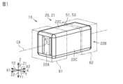
- FIG. 1 is a perspective view of an electronic component.
- FIG. 2 is a side view of the electronic component.
- FIG. 3 is a cross-sectional view taken along line 3-3 in FIG.
- FIG. 4 is an enlarged cross-sectional view of the element body.
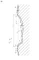
- FIG. 5 is an enlarged cross-sectional view of the recess.
- FIG. 6 is an explanatory diagram for explaining the manufacturing process of the electronic component.
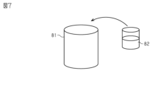
- FIG. 7 is an explanatory diagram for explaining a method for manufacturing an electronic component.
- FIG. 8 is an explanatory diagram for explaining a method for manufacturing an electronic component.
- FIG. 9 is an explanatory diagram for explaining a method for manufacturing an electronic component.
- FIG. 10 is an explanatory diagram for explaining a method for manufacturing an electronic component.
- the electronic component 10 is, for example, a surface-mount type negative temperature coefficient thermistor component that is mounted on a circuit board, etc. Note that a negative temperature coefficient thermistor component has a characteristic that its resistance value decreases as the temperature increases.
- the electronic component 10 includes an element body 20.
- the element body 20 is generally rectangular and has a central axis CA.
- an axis extending along the central axis CA is referred to as a first axis X.
- One of the axes perpendicular to the first axis X is referred to as a second axis Y.
- An axis perpendicular to the first axis X and the second axis Y is referred to as a third axis Z.
- One of the directions along the first axis X is referred to as a first positive direction X1
- the direction along the first axis X opposite to the first positive direction X1 is referred to as a first negative direction X2.
- One of the directions along the second axis Y is referred to as a second positive direction Y1, and the direction along the second axis Y opposite to the second positive direction Y1 is referred to as a second negative direction Y2.
- One of the directions along the third axis Z is referred to as a third positive direction Z1, and the direction along the third axis Z opposite to the third positive direction Z1 is referred to as a third negative direction Z2.
- the outer surface 21 of the element body 20 has six flat surfaces. Note that the "surface" of the element body 20 here refers to what can be observed as a surface when the element body 20 is observed as a whole. In other words, even if there are minute irregularities or steps that can only be seen by magnifying and observing a part of the element body 20 with a microscope, for example, it is expressed as a flat or curved surface.
- the six flat surfaces face in different directions.
- the six flat surfaces are broadly divided into a first end surface 22A facing the first positive direction X1, a second end surface 22B facing the first negative direction X2, and four side surfaces 22C.
- the four side surfaces 22C are a surface facing the third positive direction Z1, a surface facing the third negative direction Z2, a surface facing the second positive direction Y1, and a surface facing the second negative direction Y2.
- the boundary portions of two adjacent flat surfaces and the boundary portions of three adjacent flat surfaces of the outer surface 21 of the element body 20 are curved. In other words, the corners of the element body 20 are rounded and chamfered. Note that in Figures 1 and 2, the outer surface 53 of the glass film 51, which will be described later, is identified with the outer surface 21 of the element body 20 and is given a reference number.
- the element body 20 has a larger dimension along the first axis X than along the third axis Z. Also, as shown in FIG. 1, the element body 20 has a larger dimension along the first axis X than along the second axis Y. Also, the material of the element body 20 is a ceramic obtained by sintering a metal oxide containing one or more elements selected from Mn, Fe, Ni, Co, Ti, Ba, Al, and Zn. Therefore, as shown in FIG. 4, the element body 20 has a plurality of voids 23 inside. These voids 23 exist mainly at the boundaries of the grains that make up the element body 20, which is a sintered body. Note that the voids 23 are not shown in FIG. 3.
- the electronic component 10 has two first internal electrodes 41 and two second internal electrodes 42.
- the first internal electrodes 41 and the second internal electrodes 42 are both embedded inside the element body 20.
- the material of the first internal electrode 41 is a conductive material.
- the material of the first internal electrode 41 is palladium.
- the material of the second internal electrode 42 is the same as the material of the first internal electrode 41.
- the first internal electrode 41 has a rectangular plate shape.
- the main surface of the first internal electrode 41 is perpendicular to the second axis Y.
- the second internal electrode 42 has the same rectangular plate shape as the first internal electrode 41.
- the main surface of the second internal electrode 42 is perpendicular to the second axis Y, similar to the first internal electrode 41.
- the dimension of the first internal electrode 41 in the direction along the first axis X is smaller than the dimension of the element body 20 in the direction along the first axis X. Also, as shown in FIG. 1, the dimension of the first internal electrode 41 in the direction along the third axis Z is approximately two-thirds of the dimension of the element body 20 in the direction along the third axis Z. The dimensions of the second internal electrode 42 in each direction are the same as those of the first internal electrode 41.
- the first internal electrodes 41 and the second internal electrodes 42 are positioned alternately in the direction along the second axis Y. That is, they are arranged in the order of the first internal electrode 41, the second internal electrode 42, the first internal electrode 41, and the second internal electrode 42 in the second positive direction Y1. In this embodiment, the distances between the internal electrodes in the direction along the second axis Y are equal.
- the two first internal electrodes 41 and the two second internal electrodes 42 are both located at the center of the element body 20 in the direction along the third axis Z.
- the first internal electrode 41 is located closer to the first positive direction X1.
- the second internal electrode 42 is located closer to the first negative direction X2.
- the end of the first internal electrode 41 on the first positive direction X1 side coincides with the end of the element body 20 on the first positive direction X1 side.
- the end of the first internal electrode 41 on the first positive direction X1 side is exposed at the first end surface 22A of the element body 20.
- the end of the first internal electrode 41 on the first negative direction X2 side is located inside the element body 20 and does not reach the end of the element body 20 on the first negative direction X2 side.
- the end of the second internal electrode 42 on the first negative direction X2 side coincides with the end of the element body 20 on the first negative direction X2 side.
- the end of the first internal electrode 41 on the first negative direction X2 side is exposed at the second end surface 22B of the element body 20.
- the end of the second internal electrode 42 on the first positive direction X1 side is located inside the element body 20 and does not reach the end of the element body 20 on the first positive direction X1 side.
- the electronic component 10 includes a glass film 51.
- the glass film 51 covers the outer surface 21 of the element body 20.
- the glass film 51 covers all four side surfaces 22C of the outer surface 21 of the element body 20.
- the main material of the glass film 51 is insulating glass. Therefore, the glass film 51 contains silicon dioxide.
- the glass film 51 also contains an organosilane compound having a carbon chain with three or more carbon atoms.
- the organosilane compound has one or more functional groups selected from, for example, an epoxy group, a mercapto group, an amino group, a vinyl group, and a methacryl group.
- the organosilane compound is 3-glycidoxypropyltrimethoxysilane (hereinafter referred to as "GPTMS").
- GPTMS has an epoxy group as a functional group.
- the electronic component 10 has a filling portion 52.
- the filling portion 52 fills at least some of the voids 23. In this embodiment, it fills almost all of the voids 23 in the base body 20.
- the material of the filling portion 52 is the same as that of the glass film 51.
- the filling portion 52 fills the void 23 located closest to the geometric center GC, it can be said that the filling portion 52 fills substantially all of the voids 23 in the element body 20.
- the geometric center GC of the element body 20 is the geometric center point of the element body 20 including the first internal electrode 41 and the second internal electrode 42 located inside the element body 20.
- some deviation from the geometric center GC is allowed.
- the deviation from the geometric center GC in the strict sense is about 5% of the dimension of the element body 20 in the direction along the first axis X, it is still considered to be the geometric center GC.
- the electronic component 10 has a first external electrode 61 and a second external electrode 62. Note that in FIGS. 1 to 3, the first external electrode 61 and the second external electrode 62 are illustrated by two-dot chain lines.
- the first external electrode 61 has a first base electrode 61A and a first metal layer 61B.
- the first base electrode 61A is laminated on a portion of the outer surface 21 of the element body 20, including the first end face 22A.
- the first base electrode 61A covers the first end face 22A of the element body 20, and also covers a portion of the first positive direction X1 side of the four side faces 22C from above the glass film 51.
- the first base electrode 61A is a five-sided electrode.
- the material of the first base electrode 61A is a resin electrode. More specifically, the material of the first base electrode 61A is a mixture of organic resin and silver particles.
- the first metal layer 61B covers the first base electrode 61A from the outside. Therefore, the first metal layer 61B is laminated on the first base electrode 61A. Although not shown in the figure, the first metal layer 61B has a two-layer structure consisting of a nickel plating layer and a tin plating layer, in that order from the first base electrode 61A side.
- the first external electrode 61 is connected to the end of the first internal electrode 41 on the first positive direction X1 side.
- the second external electrode 62 has a second base electrode 62A and a second metal layer 62B.
- the second base electrode 62A is laminated on a portion of the outer surface 21 of the element body 20, including the second end face 22B.
- the second base electrode 62A covers the second end face 22B of the element body 20, and also covers a portion of the first negative direction X2 side of the four side faces 22C from above the glass film 51.
- the second base electrode 62A is a five-sided electrode.
- the material of the second base electrode 62A is a resin electrode. More specifically, the material of the second base electrode 62A is a mixture of organic resin and silver particles.
- the second metal layer 62B covers the second base electrode 62A from the outside. Therefore, the second metal layer 62B is laminated on the second base electrode 62A. Specifically, the second metal layer 62B has a two-layer structure of a nickel plating layer and a tin plating layer, similar to the first metal layer 61B.
- the second external electrode 62 is connected to the end of the second internal electrode 42 on the first negative direction X2 side.
- the second external electrode 62 does not reach the first external electrode 61 on the side surface 22C, and is disposed away from the first external electrode 61 in the direction along the first axis X.
- the first external electrode 61 and the second external electrode 62 are not laminated, and the glass film 51 is exposed.
- the maximum depth H of the recess 24 is the depth at the deepest point of the recess 24. Specifically, the maximum depth H of the recess 24 is calculated as follows. First, the element body 20 is ground in a direction perpendicular to the outer surface 21 of the element body 20. Grinding is performed, for example, by focused ion beam processing. Next, an image of the ground cross section of the element body 20 is taken using an electron microscope or the like. Then, as shown in FIG. 5, a tangent line CL is drawn on the ground cross section taken, circumscribing both of the outer surfaces 21 of the element body 20 on both sides of the recess 24. Note that a part of the tangent line CL may coincide with the outer surface 21 of the element body 20.
- the element body 20 is further ground from the ground cross section by a predetermined imaging pitch, and a new ground cross section of the element body 20 is imaged.
- the imaging pitch is, for example, 10 nm.
- the maximum depth of the same recess 24 on this new ground cross section is measured. In this manner, the imaging of the ground cross section of the element 20 and the measurement of the maximum depth of the recess 24 are repeated. The largest value among the maximum depths of the recess 24 on each ground cross section obtained in this manner is determined as the maximum depth H of the entire recess 24.
- the maximum depth H of the recess 24 calculated by the above method is 0.3 ⁇ m or more and 3 ⁇ m or less.
- the maximum dimension L of the line segment LS connecting two points on the opening edge 25 of the recess 24 is 0.5 ⁇ m or more and 20 ⁇ m or less.
- the opening edge 25 of the recess 24 is defined as follows. First, a tangent line CL is drawn on the ground cross-sectional image of the base body 20 captured using an electron microscope or the like using the method described above. Then, among the points of contact between this tangent line CL and the outer surface 21 of the base body 20, the edge closest to the center of the recess 24 is defined as the opening edge 25.
- the portion of outer surface 21 of element body 20 excluding recesses 24 is defined as flat surface 26.
- the arithmetic mean roughness of outer surface 53 of glass film 51 at the portion covering recesses 24 is greater than the arithmetic mean roughness of outer surface 53 of glass film 51 at the portion covering flat surface 26.
- the arithmetic mean roughness of the portion of outer surface 53 of glass film 51 covering recesses 24 is 3 nm or more and 200 nm or less. More preferably, the arithmetic mean roughness is 100 nm or less. Even more preferably, the arithmetic mean roughness is 10 nm or more and 30 nm or less.
- the arithmetic mean roughness of the portion of the outer surface 53 of the glass film 51 that covers the recess 24 is calculated as follows. First, a tangent line CL is drawn on the ground cross-sectional image of the element 20 captured using an electron microscope or the like by the method described above. The measurement range is then the range between the opening edges 25 of one recess 24 on the ground cross-sectional surface, and a range of 500 nm in the direction along the tangent line CL. Then, the arithmetic mean roughness of the glass film 51 at the portion that covers the recess 24 in the measurement range is calculated by image processing.
- the average thickness T2 of the glass film 51 at the portion covering the flat surface 26 is 15 nm or more and 1000 nm or less. More preferably, the average thickness T2 of the glass film 51 at the portion covering the flat surface 26 is 15 nm or more and 500 nm or less. Even more preferably, the average thickness T2 of the glass film 51 at the portion covering the flat surface 26 is 20 nm or more and 200 nm or less.
- the average value of thickness T1 of glass film 51 at the portion covering recess 24 is greater than the average value of thickness T2 of glass film 51 at the portion covering flat surface 26.
- the average value of thickness T1 of glass film 51 at the portion covering recess 24 is approximately 106 nm.
- the average value of thickness T2 of glass film 51 at the portion covering flat surface 26 is 33 nm.
- the method for manufacturing electronic component 10 includes an element body preparation step S11, an R-chamfering step S12, a solvent introduction step S13, and a catalyst introduction step S14.
- the method for manufacturing electronic component 10 also includes an element body introduction step S15, a solution introduction step S16, a filling/film-forming step S17, a drying step S18, a first curing step S19, and an internal electrode exposure step S20.
- the method for manufacturing electronic component 10 also includes a conductor application step S21, a second curing step S22, and a plating step S23.
- the element body preparation step S11 is performed.
- a rectangular parallelepiped element body 20 having six planes is prepared. That is, the element body 20 at this stage is the element body 20 in a state before R-chamfering.
- a plurality of ceramic sheets that will become the element body 20 are prepared. The sheets are thin plates. A conductive paste that will become the first internal electrode 41 is laminated on the sheets. A ceramic sheet that will become the element body 20 is laminated on the laminated paste. A conductive paste that will become the second internal electrode 42 is laminated on the sheets. In this manner, the ceramic sheet and the conductive paste are laminated. Then, the ceramic sheet is cut to a predetermined size to form the element body 20 as an unfired laminate. After that, the unfired element body 20 is fired at a high temperature to prepare the element body 20.
- the ceramic sheet has a plurality of voids inside. Therefore, the prepared element body 20 has a plurality of voids 23 inside.
- a solvent introduction step S13 is performed as shown in Fig. 6.
- a solvent introduction step S13 2-propanol is introduced into a reaction vessel 81 as a solvent 82.
- a catalyst introduction step S14 is performed as shown in Fig. 6.
- the catalyst introduction step S14 first, stirring of the solvent 82 in the reaction vessel 81 is started. Then, ammonia water is introduced into the reaction vessel 81 as an aqueous solution 83 containing a catalyst.
- the catalyst in this embodiment is a hydroxide ion, and functions as a catalyst for promoting hydrolysis of a metal alkoxide, which will be described later.
- the element introduction step S15 is performed. As shown in FIG. 9, in the element introduction step S15, a plurality of element bodies 20 that have been previously formed in the R chamfering step S12 as described above are introduced into a reaction vessel 81.
- a solution introduction step S16 is performed.
- a mixed liquid 84 of a metal alkoxide and an organosilane compound is introduced into a reaction vessel 81.
- the metal alkoxide is liquid tetraethyl orthosilicate (hereinafter referred to as "TEOS").
- TEOS is also called tetraethoxysilane.
- the organosilane compound is liquid GPTMS.
- the GPTMS is introduced in a weight ratio of 0.12 or more and less than 1 relative to the TEOS. Specifically, the GPTMS is introduced in a weight ratio of approximately 0.43 relative to the TEOS.
- the amount of mixed liquid 84 added in solution adding step S16 is calculated based on the porosity of the element body 20 and the area of the outer surface 21 of the element body 20 added in element body adding step S15. Specifically, first, for each element body 20, the sum of the amount of the solution required to fill the voids 23 of the element body 20 and the amount of the solution required to form a glass film 51 covering the outer surface 21 of the element body 20 is calculated. This sum is multiplied by the number of element bodies 20 added in element body adding step S15 to calculate the required amount of mixed liquid 84.
- the porosity of the element body 20 is defined as the ratio of the total volume of the voids 23 to the volume of the element body 20.
- the filling/film-forming step S17 is performed.
- the stirring of the solvent 82 that was started in the solvent introduction step S13 is continued for a predetermined time.
- the metal alkoxide undergoes condensation polymerization by hydrolysis with hydroxide ions, which serve as a catalyst.
- the metal alkoxide particles generated by this condensation polymerization reaction maintain a small volume per molecule for a relatively long period of time. Therefore, first, a portion of the metal alkoxide enters the voids 23 inside the element 20 together with the solution. Thereafter, the condensation polymerization of the metal alkoxide progresses within the voids 23, causing the metal alkoxide particles to grow larger. As a result, a filling portion 52 is formed within the voids 23 of the element 20.
- the metal alkoxide that did not penetrate the voids 23 undergoes condensation polymerization outside the base body 20, causing the particles to grow larger.
- the metal alkoxide particles then associate with the organosilane compound. That is, the metal alkoxide particles are bonded to each other by intermolecular forces.
- the associated metal alkoxide adheres to the outer surface 21 of the base body 20.
- the metal alkoxides attached to the outer surface 21 of the base body 20 then undergo condensation polymerization to form a glass film 51.
- the metal alkoxide and the solvent 82 are likely to come into contact with each other on the flat surface 26 of the outer surface 21 of the base body 20.
- the outer surface 53 of the glass film 51 covering the flat surface 26 is smoothed to a certain extent.
- the metal alkoxide and the solvent 82 are unlikely to come into contact with each other on the inner surface of the recess 24. Therefore, the surface roughness of the outer surface 53 of the glass film 51 covering the recess 24 reflects the shape of the metal alkoxide association that has accumulated on the inner surface of the recess 24, and is rougher than the surface roughness of the glass film 51 covering the flat surface 26.
- a sol-like filling portion 52 is formed by a liquid-phase reaction in the reaction vessel 81, and a sol-like glass film 51 is formed. Furthermore, the arithmetic mean roughness of the outer surface 53 of the glass film 51 at the portion covering the flat surface 26 of the outer surface 21 of the element body 20 is smaller than the arithmetic mean roughness of the outer surface 53 of the glass film 51 at the portion covering the recess 24.
- the drying step S18 is performed.
- the element body 20 is removed from the reaction vessel 81.
- the filling portion 52 on the sol and the sol-like glass film 51 are dried. As a result, a gel-like filling portion 52 and a gel-like glass film 51 are formed.
- a first hardening step S19 is performed.
- the base body 20 that has undergone the drying step S18 is baked at a temperature of 140 degrees or more and 160 degrees or less. Specifically, it is baked at a temperature of 150 degrees. This hardens the gel-like filling portion 52 and the gel-like glass film 51. In other words, the entire glass film 51 and filling portion 52 are hardened. At this stage, the glass film 51 covers the entire outer surface 21 of the base body 20.
- the internal electrode exposure process S20 is performed.
- the glass film 51 covering the first end face 22A and the second end face 22B of the element body 20 is removed to expose the first internal electrode 41 and the second internal electrode 42.
- the glass film 51 is removed by grinding with a laser from the entire area of the first end face 22A and the entire area of the second end face 22B of the element body 20.
- the conductor application step S21 is performed.
- a conductor paste is applied to a portion of the outer surface 21 of the element body 20 and a portion of the outer surface 53 of the glass film 51.
- the conductor paste is applied to two locations: the glass film 51 covering the first end face 22A of the element body 20 and a portion of the four side faces 22C of the element body 20 on the first positive direction X1 side, and the glass film 51 covering the second end face 22B of the element body 20 and a portion of the four side faces 22C of the element body 20 on the first negative direction X2 side.
- the conductor paste contains silver particles and an organic resin.
- a second curing step S22 is performed. Specifically, in the second curing step S22, the base body 20 to which the conductive paste has been applied is heated to harden the conductive paste. In this embodiment, the base body 20 is heated to about 200 degrees. Then, the conductive paste applied in the conductor application step S21 is fired to form the first base electrode 61A and the second base electrode 62A.
- the plating process S23 is performed.
- a first metal layer 61B is formed on the surface of the first base electrode 61A by electroplating.
- a second metal layer 62B is formed on the surface of the second base electrode 62A.
- the first metal layer 61B and the second metal layer 62B are electroplated with two types of metal, nickel and tin, to form a two-layer structure. In this manner, the electronic component 10 is formed.
- the arithmetic mean roughness of the portion of outer surface 53 of glass film 51 covering recess 24 is 3 nm or more and 200 nm or less.
- Outer surface 53 of glass film 51 has a certain degree of hydrophobicity and oleophobicity.
- the arithmetic mean roughness of glass film 51 is within the above range, liquid is unlikely to penetrate into the gaps between the minute projections and recesses on outer surface 53 of glass film 51. Therefore, the barrier property against liquid of glass film 51 covering recess 24 can be improved.
- the arithmetic mean roughness of the outer surface 53 of the glass film 51 is greater than 200 nm, friction is more likely to occur on the outer surface 53 of the glass film 51, and there is a risk of cracks or the like occurring in the glass film 51. Therefore, the arithmetic mean roughness of the portion of the outer surface 53 of the glass film 51 that covers the recess 24 is preferably within the above numerical range.
- the average value of the thickness T2 of the glass film 51 at the portion covering the flat surface 26 of the outer surface 21 of the element body 20 is 15 nm or more and 1000 nm or less. If the thickness T2 of the glass film 51 is less than 15 nm, there is a risk that plating solution and the like may easily penetrate. Furthermore, if the thickness T2 of the glass film 51 is greater than 1000 nm, the stress acting on the glass film 51 is likely to be large. In other words, there is a risk that cracks and the like may easily occur in the glass film 51. Therefore, the above numerical range is preferable for the thickness T2 of the glass film 51.
- the average value of the thickness T1 of the glass film 51 covering the recess 24 is greater than the average value of the thickness T2 of the glass film 51 covering the flat surface 26.
- the thinner the thickness T1 of the glass film 51 covering the recess 24 the lower the barrier property of the glass film 51 against liquids in the recess 24.
- the average value of the thickness T1 of the glass film 51 covering the recess 24 greater than the average value of the thickness T2 of the glass film 51 covering the flat surface 26, it is possible to prevent cracks from occurring in the portions other than the recess 24 while ensuring sufficient barrier property of the glass film 51 against liquids.
- the maximum dimension L of the line segment LS connecting two points on the opening edge 25 of the recess 24 is 0.5 ⁇ m or more and 20 ⁇ m or less.
- the maximum dimension of the outer diameter of the recess 24 is 0.5 ⁇ m or more and 20 ⁇ m or less. If the above maximum dimension L is less than 0.5 ⁇ m, there is a risk that the glass film 51 will be difficult to form on the surface of the recess 24. Furthermore, if the above maximum dimension L is greater than 0.5 ⁇ m, the arithmetic mean roughness of the portion of the outer surface 53 of the glass film 51 that covers the recess 24 is likely to be small. Therefore, the above numerical range is preferable for the maximum dimension of the outer diameter of the opening edge 25 of the recess 24.
- the maximum depth H of the recess 24 is 0.3 ⁇ m or more and 3 ⁇ m or less. If the maximum depth H of the recess 24 is less than 0.3 ⁇ m, the arithmetic mean roughness of the outer surface 53 of the glass film 51 covering the recess 24 is unlikely to be in the suitable numerical range as described in section (1). Also, if the maximum depth H of the recess 24 is greater than 3 ⁇ m, for example, in a portion where the inner surface of the recess 24 has a steep slope, the arithmetic mean roughness of the outer surface 53 of the glass film 51 is unlikely to be in the suitable numerical range as described in section (1). Therefore, the above numerical range is preferable for the maximum depth H of the recess 24.
- the organosilane compound is a silane compound having a carbon chain with three or more carbon atoms. This makes it easier for the arithmetic mean roughness of the outer surface 53 of the glass film 51 covering the recess 24 to fall within a suitable numerical range.
- the arithmetic mean roughness of the outer surface 53 of the glass film 51 covering the recess 24 is 3 nm or more and 200 nm or less. Therefore, the barrier properties against liquids in the recess 24 can be improved without making the glass film 51 excessively thick.
- the electronic component 10 is not limited to a negative temperature coefficient thermistor component.
- the electronic component 10 may be a thermistor component other than a negative temperature coefficient thermistor component, a multilayer capacitor component, or an inductor component.
- the material of the element body 20 is not limited to the example in the above embodiment.
- the material of the element body 20 may be a composite of resin and metal powder, fiber, thermosetting resin, or the like.
- the shape of the element body 20 is not limited to the example of the above embodiment.
- the element body 20 may be a polygonal columnar shape other than a quadrangular columnar shape having a central axis CA.
- the element body 20 may also be a core of a wire-wound inductor component.
- the core may have a so-called drum core shape.
- the core may have a columnar winding core portion and flange portions provided at each end of the winding core portion.
- the boundary portion between adjacent flat surfaces of the outer surface 21 of the element body 20 does not have to be chamfered. In this case, no curved surface exists at the boundary portion.
- the first internal electrode 41 and the second internal electrode 42 may have any shape as long as they can ensure electrical conduction with the corresponding first external electrode 61 and second external electrode 62. Furthermore, the number of first internal electrodes 41 and second internal electrodes 42 does not matter, and the number of internal electrodes may be one, or three or more.
- the configuration of the first external electrode 61 is not limited to the example of the above embodiment.
- the first external electrode 61 may be composed of only the first base electrode 61A, and the first metal layer 61B may not have a two-layer structure. The same applies to the second external electrode 62.
- the materials of the first internal electrode 41, the second internal electrode 42, the first external electrode 61, and the second external electrode 62 are not important. It is only necessary to ensure electrical conduction between the first internal electrode 41 and the second internal electrode 42 and the corresponding first external electrode 61 and second external electrode 62.
- the material of the first internal electrode 41 and the second internal electrode 42 may be a conductive material such as silver or copper.
- the material of the first external electrode 61 and the second external electrode 62 does not have to be a resin electrode.
- it may be an electrode made of a mixture of silver and glass that does not contain resin.
- the material of the conductive filler mixed with the resin in the first external electrode 61 and the second external electrode 62 is not limited to silver. For example, it may be copper.
- the location of the first external electrode 61 is not limited to the example of the above embodiment.
- the first external electrode 61 may be disposed only on the first end surface 22A and one side surface 22C.
- the configuration of the glass film 51 is not limited to the example of the above embodiment.
- the area covered by the glass film 51 may be changed as appropriate in accordance with the shape of the element body 20, the positions of the first external electrode 61 and the second external electrode 62, etc.
- the glass contained in the glass film 51 may be diffused into the glass in the first base electrode 61A.
- the glass film 51 and the glass contained in the first base electrode 61A may be integrated.
- the second base electrode 62A may be integrated.
- the organic silane compound is not limited to GPTMS.
- the organic silane compound may not have any of an epoxy group, a mercapto group, an amino group, a vinyl group, or a methacryl group.
- the organic silane compound may be an organic silane compound such as 3-aminopropyltrimethoxysilane, 3-aminopropyltriethoxysilane, 3-(2-aminoethyl)aminopropyltrimethoxysilane, 3-phenylaminopropyltrimethoxysilane, (3-glycidoxypropyl)methyldimethoxysilane, 3-methacryloxypropyltrimethoxysilane, 3-methacryloxypropylmethyldimethoxysilane, 3-mercaptopropyltrimethoxysilane, n-propyltrimethoxysilane, isobutyltrimethoxysilane, n-hexyltrimethoxysilane,
- the organic silane compound may not have a carbon chain with 3 or more carbon atoms.
- the presence of an organic silane compound in the glass film 51 can be identified by using methods such as X-ray photoelectron spectroscopy (XPS), Fourier transform infrared spectroscopy, Raman spectroscopy, and energy dispersive X-ray analysis.
- XPS X-ray photoelectron spectroscopy
- Raman spectroscopy Raman spectroscopy
- energy dispersive X-ray analysis energy dispersive X-ray analysis.
- the filling portion 52 does not have to fill the gap 23 closest to the geometric center GC of the element body 20. In other words, it is sufficient that the filling portion 52 fills at least a portion of the gap 23 of the element body 20. Also, the electronic component 10 does not have to have a filling portion 52, and it is sufficient that it has at least a glass film 51.
- the maximum depth H of the recess 24 may be smaller than 0.3 ⁇ m or larger than 3 ⁇ m. Even in these cases, the effect described in (1) can be obtained as long as the arithmetic mean roughness of the portion of the outer surface 53 of the glass film 51 covering the recess 24 is 3 nm or more and 200 nm or less.
- the maximum dimension L of the line segment LS connecting two points on the opening edge 25 of the recess 24 may be smaller than 0.5 ⁇ m or larger than 20 ⁇ m. Even in these cases, the effect described in (1) can be obtained.
- the arithmetic mean roughness of the outer surface 53 of the glass film 51 at the portion covering the flat surface 26 does not have to be smaller than the arithmetic mean roughness of the outer surface 53 of the glass film 51 at the portion covering the recess 24.
- the arithmetic mean roughness of the outer surface 53 of the glass film 51 at least at the portion covering the recess 24 is 3 nm or more and 200 nm or less, the effect described in (1) can be obtained.
- the average value of the thickness T2 of the glass film 51 at the portion covering the flat surface 26 may be smaller than 15 nm or larger than 1000 nm. Even if the thickness T2 of the glass film 51 is in this range, the effect described in (1) can be obtained as long as the arithmetic mean roughness of the glass film 51 covering the recess 24 is within a predetermined range.
- the solvent 82 introduced in the solvent introduction step S13 is not limited to the example in the above embodiment, and may be any liquid capable of dispersing the metal alkoxide appropriately.
- the solvent introduction step S13 may be performed after the catalyst introduction step S14 or the base introduction step S15.
- the solvent introduction step S13 may be performed prior to at least one of the solution introduction step S16 and the catalyst introduction step S14.
- the solvent introduction step S13 may also be omitted. In this case, for example, if the amount of water contained in the aqueous solution 83 containing the catalyst is appropriately large, the metal alkoxide will react in the liquid phase.
- the aqueous solution 83 containing the catalyst may also be introduced in a state where it is mixed with an organic solvent as the solvent 82.
- the aqueous solution 83 containing a catalyst is ammonia water, and the catalyst is hydroxide ions, but the catalyst is not limited to this. If the aqueous solution is basic, it can promote the hydrolysis of metal alkoxide as a catalyst, just like the ammonia water in the above embodiment. Even if the aqueous solution is acidic, it can promote the hydrolysis of metal alkoxide as a catalyst. Furthermore, even if the aqueous solution is neutral, it can be sufficient if it contains a substance that functions as a catalyst, such as ions that can promote hydrolysis.
- a solid compound containing the catalyst and water may be added separately to the reaction vessel 81.
- the catalyst can be considered to have been added to the reaction vessel 81 when it is produced in the reaction vessel 81.
- a solid compound containing the catalyst may be added to the reaction vessel 81, and moisture in the air may be used as the water required for hydrolysis.
- the base body introduction step S15 may be performed prior to the catalyst introduction step S14. Also, if the base body introduction step S15 is performed prior to the catalyst introduction step S14, the solution introduction step S16 may be performed prior to the catalyst introduction step S14 or the base body introduction step S15. At the very least, the base body introduction step S15 needs to be performed prior to either the solution introduction step S16 or the catalyst introduction step S14.
- a solution containing a precursor for generating a metal alkoxide may be introduced instead of a metal alkoxide.
- a metal complex or acetate which is a metal alkoxide precursor, may be introduced in the solution introduction step S16.
- metal complexes include acetylacetonates such as lithium acetylacetonate, titanium (IV) oxyacetylacetonate, titanium diisopropoxide bis(acetylacetonate), zirconium (IV) trifluoroacetylacetonate, zirconium (IV) acetylacetonate, aluminum acetylacetonate, aluminum (III) acetylacetonate, calcium (II) acetylacetonate, and zinc (II) acetylacetonate.
- acetates include zirconium acetate, zirconium (IV) hydroxide acetate, and basic aluminum acetate.
- the metal alkoxide may be generated inside the reaction vessel 81 instead of being introduced into the reaction vessel 81 after generating the metal alkoxide outside the reaction vessel 81.
- the metal alkoxide is generated by reacting a metal salt with an alcohol. Therefore, when a metal salt and an alcohol, which are metal alkoxide precursors, are input into the reaction vessel 81 and react with each other to generate the metal alkoxide, the metal alkoxide can be considered to have been input into the reaction vessel 81.
- ⁇ Metal alkoxides are not limited to TEOS.
- the metal contained in the metal alkoxide may be titanium, zirconium, aluminum, etc. If the metal contained in the metal alkoxide is silicon, the reaction rate is slower than other metals, making it easier to control the reaction rate of the metal alkoxide to a constant value.
- the alkoxy group of the metal alkoxide may be a methoxy group, a propoxy group, or the like, or may be modified with a functional group such as a long-chain alkyl group or an epoxy group as in a coupling agent.
- the coordination number for the metal contained in the metal alkoxide is not limited to 4-coordination, and may be 3-coordination or 2-coordination.
- the mixed solution 84 of the metal alkoxide and the organosilane compound does not need to be mixed in advance.
- the metal alkoxide and the organosilane compound may be individually introduced into the reaction vessel 81 in a predetermined ratio.
- the weight ratio of the organosilane compound to the metal alkoxide introduced into the reaction vessel 81 is not limited to the example in the above embodiment.
- the first curing step S19 does not have to be performed after the drying step S18.
- the glass film 51 may be cured together with the firing of the conductive paste.
- the method for removing the glass film 51 is not limited to laser cutting.
- the first internal electrode 41 and the second internal electrode 42 may be exposed using methods such as ion milling and polishing.
- the range of glass film 51 to be removed is not limited to the example of the above embodiment.
- the second curing step S22 is not limited to heating the conductive paste.
- a material that is cured by exposure to ultraviolet light is used as the conductive paste, it may be cured by exposure to ultraviolet light.
- the material of the conductive paste is not limited to resin.
- the material of the glass film contains an organic silane compound,
- the outer surface of the body has a recess that is recessed relative to the surrounding area,
- the electronic component has an arithmetic mean roughness of the outer surface of the glass film at a portion covering the recess, the arithmetic mean roughness being 3 nm or more and 200 nm or less.
Landscapes
- Engineering & Computer Science (AREA)
- Power Engineering (AREA)
- Microelectronics & Electronic Packaging (AREA)
- Physics & Mathematics (AREA)
- Electromagnetism (AREA)
- Manufacturing & Machinery (AREA)
- Fixed Capacitors And Capacitor Manufacturing Machines (AREA)
Abstract
電子部品(10)は、素体(20)と、ガラス膜(51)と、を備える。ガラス膜(51)は、素体(20)の外表面(21)を覆っている。ガラス膜(51)の材質は、有機シラン化合物を含む。素体(20)の外表面(21)は、周囲に対して窪んだ箇所である凹部(24)を有している。ガラス膜(51)の外表面(53)のうち、凹部(24)を覆う箇所の算術平均粗さは、3nm以上200nm以下である。
Description
本開示は、電子部品に関する。
特許文献1に開示されている電子部品は、素体と、ガラス膜と、を備える。ガラス膜は、素体の外表面を覆っている。
特許文献1に開示されているような電子部品において、素体の外表面は、周囲に対して窪んだ箇所である凹部を有していることがある。当該凹部の内面においては、凹部が形成される過程において微細な隙間及びクラック等が生じている可能性がある。そのため、当該凹部からは、素体の内部にめっき液等の液体が侵入しやすい。凹部から素体内部に液体が侵入してしまうことを抑制するためには、凹部を覆うガラス膜の、液体に対するバリア性を高める必要がある。
上記課題を解決するため、本開示の一態様は、素体と、素体の外表面を覆うガラス膜と、を備え、前記ガラス膜の材質は、有機シラン化合物を含み、前記素体の外表面は、周囲に対して窪んだ箇所である凹部を有し、前記ガラス膜の外表面のうち、前記凹部を覆う箇所の算術平均粗さは、3nm以上200nm以下である電子部品である。
凹部を覆うガラス膜の、液体に対するバリア性を高められる。
<電子部品の一実施形態>
以下、電子部品の一実施形態を、図面を参照して説明する。なお、図面は、理解を容易にするために構成要素を拡大して示している場合がある。構成要素の寸法比率は実際のものと、又は別の図面中のものと異なる場合がある。
以下、電子部品の一実施形態を、図面を参照して説明する。なお、図面は、理解を容易にするために構成要素を拡大して示している場合がある。構成要素の寸法比率は実際のものと、又は別の図面中のものと異なる場合がある。
(全体構成について)
図1に示すように、電子部品10は、例えば、回路基板等に実装される表面実装型の負特性サーミスタ部品である。なお、負特性サーミスタ部品は、温度が上がると抵抗値が下がるという特性を有するものである。
図1に示すように、電子部品10は、例えば、回路基板等に実装される表面実装型の負特性サーミスタ部品である。なお、負特性サーミスタ部品は、温度が上がると抵抗値が下がるという特性を有するものである。
電子部品10は、素体20を備えている。素体20は、略四角柱状であり、中心軸線CAを有する。なお、以下では、中心軸線CAに沿って延びる軸を第1軸Xとする。また、第1軸Xに直交する軸の1つを第2軸Yとする。そして、第1軸X及び第2軸Yに直交する軸を第3軸Zとする。さらに、第1軸Xに沿う方向の一方を第1正方向X1とし、第1軸Xに沿う方向のうち第1正方向X1と反対方向を第1負方向X2とする。また、第2軸Yに沿う方向の一方を第2正方向Y1とし、第2軸Yに沿う方向のうち第2正方向Y1と反対方向を第2負方向Y2とする。さらに、第3軸Zに沿う方向の一方を第3正方向Z1とし、第3軸Zに沿う方向のうち第3正方向Z1と反対方向を第3負方向Z2とする。
素体20の外表面21は、6個の平面を有している。なお、ここでいう素体20の「面」とは、素体20全体を観察したときに面として観察できるものをいう。つまり、例えば素体20の一部を顕微鏡等で拡大して観察しなければわからないような微小な凹凸、段差が存在しても、平面又は曲面と表現する。
6個の平面は、互いに異なる方向を向いている。6個の平面は、第1正方向X1を向く第1端面22Aと、第1負方向X2を向く第2端面22Bと、4つの側面22Cに大別される。4つの側面22Cは、それぞれ、第3正方向Z1を向く面と、第3負方向Z2を向く面と、第2正方向Y1を向く面と、第2負方向Y2を向く面と、である。
素体20の外表面21のうち、隣り合う2つの平面の境界部分、及び隣り合う3つの平面の境界部分は、曲面になっている。すなわち、素体20の角は、R面取り形状になっている。なお、図1及び図2では、後述するガラス膜51の外表面53を、素体20の外表面21と同一視して符号を付している。
図2に示すように、素体20は、第1軸Xに沿う方向の寸法が、第3軸Zに沿う方向の寸法よりも大きい。また、図1に示すように、素体20は、第1軸Xに沿う方向の寸法が、第2軸Yに沿う方向の寸法よりも大きい。また、素体20の材質は、Mn、Fe、Ni、Co、Ti、Ba、Al、及びZnから選ばれる1以上を成分とする金属酸化物を焼成したセラミックスである。そのため、図4に示すように、素体20は、内部に複数の空隙23を有している。これら空隙23は、主に、焼結体である素体20を構成する粒子の境界に存在している。なお、図3においては、空隙23の図示を省略している。
図3に示すように、電子部品10は、2つの第1内部電極41と、2つの第2内部電極42と、を備えている。第1内部電極41及び第2内部電極42は、いずれも素体20の内部に埋め込まれている。
第1内部電極41の材質は、導電性の材料である。例えば、第1内部電極41の材質は、パラジウムである。また、第2内部電極42の材質は、第1内部電極41の材質と同一である。
第1内部電極41の形状は、長方形板状である。第1内部電極41の主面は、第2軸Yに直交している。第2内部電極42の形状は、第1内部電極41と同じ長方形板状である。第2内部電極42の主面は、第1内部電極41と同様に、第2軸Yに直交している。
第1内部電極41の第1軸Xに沿う方向の寸法は、素体20の第1軸Xに沿う方向の寸法より小さくなっている。また、図1に示すように、第1内部電極41の第3軸Zに沿う方向の寸法は、素体20の第3軸Zに沿う方向の寸法の略3分の2となっている。第2内部電極42の各方向の寸法は、第1内部電極41と同じ寸法となっている。
図3に示すように、第1内部電極41と第2内部電極42とは、第2軸Yに沿う方向に互い違いに位置している。すなわち、第2正方向Y1に向かって、第1内部電極41、第2内部電極42、第1内部電極41、第2内部電極42の順に並んでいる。本実施形態では、各内部電極間の第2軸Yに沿う方向の距離は、等しくなっている。
図1に示すように、2つの第1内部電極41及び2つの第2内部電極42は、いずれも、第3軸Zに沿う方向において、素体20の中央に位置している。その一方で、図3に示すように、第1内部電極41は、第1正方向X1に寄って位置している。第2内部電極42は、第1負方向X2に寄って位置している。
具体的には、第1内部電極41の第1正方向X1側の端は、素体20の第1正方向X1側の端と一致している。つまり、第1内部電極41の第1正方向X1側の端は、素体20の第1端面22Aにおいて露出している。そして、第1内部電極41の第1負方向X2側の端は、素体20の内部に位置しており、素体20の第1負方向X2側の端にまで至っていない。一方で、第2内部電極42の第1負方向X2側の端は、素体20の第1負方向X2側の端と一致している。つまり、第1内部電極41の第1負方向X2側の端は、素体20の第2端面22Bにおいて露出している。第2内部電極42の第1正方向X1側の端は、素体20の内部に位置しており、素体20の第1正方向X1側の端にまで至っていない。
図3に示すように、電子部品10は、ガラス膜51を備えている。ガラス膜51は、素体20の外表面21を覆っている。本実施形態においては、ガラス膜51は、素体20の外表面21のうち、4つの側面22Cをすべて覆っている。ガラス膜51の主な材質は、絶縁性のガラスである。したがって、ガラス膜51は、二酸化ケイ素を含んでいる。また、ガラス膜51は、炭素数が3以上の炭素鎖を有する有機シラン化合物を含んでいる。有機シラン化合物は、例えば、エポキシ基、メルカプト基、アミノ基、ビニル基、メタクリル基、から選ばれる1種類以上の官能基を有している。具体的には、有機シラン化合物は、3-グリシドキシプロピルトリメトキシシラン(以下、「GPTMS」という。)である。なお、GPTMSは、官能基としてエポキシ基を有している。
図4に示すように、電子部品10は、充填部52を備えている。充填部52は、少なくとも一部の空隙23に充填されている。本実施形態においては、素体20の略全ての空隙23を埋めている。充填部52の材質は、ガラス膜51と同一である。
電子顕微鏡等を用いて素体20の幾何中心GCを含む断面を撮像した場合に、充填部52が上記幾何中心GCに最も近い位置にある空隙23を埋めていれば、充填部52が素体20の略全ての空隙23を埋めているといえる。なお、図3に示すように、素体20の幾何中心GCとは、素体20の内部に位置している第1内部電極41及び第2内部電極42を含めた素体20の幾何学的な中心点である。ただし、素体20を切断する際の加工精度などによって、幾何中心GCから多少ずれることは許容される。具体的には、厳密な意味での幾何中心GCに対して、第1軸Xに沿う方向での素体20の寸法の5%程度ずれていても、幾何中心GCであるとみなす。この点、第2軸Yに沿う方向、及び第3軸Zに沿う方向のずれについても同様である。
図3に示すように、電子部品10は、第1外部電極61と、第2外部電極62と、を備えている。なお、図1~図3では、第1外部電極61及び第2外部電極62を、二点鎖線で図示している。
第1外部電極61は、第1下地電極61Aと、第1金属層61Bと、を有している。第1下地電極61Aは、素体20の外表面21のうち、第1端面22Aを含む一部分に積層されている。具体的には、第1下地電極61Aは、素体20の第1端面22Aを覆い、且つ、4つの側面22Cの第1正方向X1側の一部をガラス膜51の上から覆っている。すなわち、第1下地電極61Aは、5面電極である。この実施形態では、第1下地電極61Aの材質は、樹脂電極である。より具体的には、第1下地電極61Aの材質は、有機樹脂と銀粒子との混合物である。
第1金属層61Bは、第1下地電極61Aを外部から覆っている。そのため、第1金属層61Bは、第1下地電極61Aに積層されている。図示は省略するが、第1金属層61Bは、第1下地電極61A側から順に、ニッケルめっき層と、錫めっき層と、の2層構造となっている。なお、第1外部電極61は、第1内部電極41における第1正方向X1側の端と接続している。
第2外部電極62は、第2下地電極62Aと、第2金属層62Bと、を有している。第2下地電極62Aは、素体20の外表面21のうち、第2端面22Bを含む一部分に積層されている。具体的には、第2下地電極62Aは、素体20の第2端面22Bを覆い、且つ、4つの側面22Cの第1負方向X2側の一部をガラス膜51の上から覆っている。すなわち、第2下地電極62Aは、5面電極である。この実施形態では、第2下地電極62Aの材質は、樹脂電極である。より具体的には、第2下地電極62Aの材質は、有機樹脂と銀粒子の混合物である。
第2金属層62Bは、第2下地電極62Aを外部から覆っている。そのため、第2金属層62Bは、第2下地電極62Aに積層されている。具体的には、第2金属層62Bは、第1金属層61Bと同様に、ニッケルめっき層と、錫めっき層と、の2層構造となっている。なお、第2外部電極62は、第2内部電極42における第1負方向X2側の端と接続している。
第2外部電極62は、側面22C上において、第1外部電極61にまでは至っておらず、第1外部電極61に対して第1軸Xに沿う方向に離れて配置されている。そして、素体20の側面22C上において、第1軸Xに沿う方向の中央部分は、第1外部電極61及び第2外部電極62が積層されておらず、ガラス膜51が露出している。
(凹部について)
図5に示すように、素体20の外表面21は、1つ以上の凹部24を有している。凹部24は、周囲に対して素体20の内部側へと窪んでいる。また、上述したガラス膜51は、素体20の外表面21のうちの凹部24も覆っている。そして、ガラス膜51は、凹部24の窪んだ形状に、ある程度追従している。つまり、凹部24を覆うガラス膜51の外表面53は、周囲に対して素体20の内部側へと窪んでいる。なお、凹部24は、セラミックス粒子の脱落、素体20の割れ及び欠けなどに起因している。また、素体20の外表面21の算術平均粗さの10倍以上の最大深さHを有するものを、凹部24と定義する。
図5に示すように、素体20の外表面21は、1つ以上の凹部24を有している。凹部24は、周囲に対して素体20の内部側へと窪んでいる。また、上述したガラス膜51は、素体20の外表面21のうちの凹部24も覆っている。そして、ガラス膜51は、凹部24の窪んだ形状に、ある程度追従している。つまり、凹部24を覆うガラス膜51の外表面53は、周囲に対して素体20の内部側へと窪んでいる。なお、凹部24は、セラミックス粒子の脱落、素体20の割れ及び欠けなどに起因している。また、素体20の外表面21の算術平均粗さの10倍以上の最大深さHを有するものを、凹部24と定義する。
凹部24の最大深さHは、凹部24の最深箇所での深さである。具体的には、凹部24の最大深さHは、次のようにして算出する。まず、素体20を、当該素体20の外表面21に直交する方向に研削する。研削は、例えば集束イオンビーム加工により行う。次いで、電子顕微鏡等を用いて、素体20の研削断面を撮像する。そして、図5に示すように、当該撮像した研削断面において、凹部24を挟んだ両側の素体20の外表面21のいずれにも外接する接線CLを引く。なお、当該接線CLの一部は素体20の外表面21と一致していてもよい。このとき、当該接線CLに直交する方向において、当該接線CLから凹部24の内面までの長さを、凹部24の深さとする。続いて、上記の研削断面から所定の撮像ピッチの分だけ素体20を更に研削することで、素体20の新たな研削断面を撮像する。なお、撮像のピッチは、例えば10nmである。この新たな研削断面における同一の凹部24の最大の深さを測定する。このようにして、素体20の研削断面の撮像及び凹部24の最大の深さの測定を繰り返す。これにより得られた各研削断面における凹部24の最大の深さのうち、最も大きな値を、その凹部24全体での最大深さHとする。
上記の方法により算出した凹部24の最大深さHは、0.3μm以上、且つ3μm以下である。また、凹部24の開口縁25上の2点間を結ぶ線分LSのうち、最大の寸法Lは、0.5μm以上、且つ20μm以下である。
凹部24の開口縁25は、以下のように定義する。まず、上述した方法により、電子顕微鏡等を用いて撮像した素体20の研削断面像において、接線CLを引く。そして、この接線CLと素体20の外表面21との接点のうち、凹部24の中央側の端を、開口縁25とする。
(凹部を覆うガラス膜について)
素体20の外表面21のうち凹部24を除く部分を平坦面26とする。このとき、凹部24を覆う箇所におけるガラス膜51の外表面53の算術平均粗さは、平坦面26を覆う箇所におけるガラス膜51の外表面53の算術平均粗さよりも大きい。また、ガラス膜51の外表面53のうち、凹部24を覆う箇所の算術平均粗さは、3nm以上、且つ200nm以下である。より好ましくは、当該算術平均粗さは、100nm以下である。さらに好ましくは、当該算術平均粗さは、10nm以上、且つ30nm以下である。
素体20の外表面21のうち凹部24を除く部分を平坦面26とする。このとき、凹部24を覆う箇所におけるガラス膜51の外表面53の算術平均粗さは、平坦面26を覆う箇所におけるガラス膜51の外表面53の算術平均粗さよりも大きい。また、ガラス膜51の外表面53のうち、凹部24を覆う箇所の算術平均粗さは、3nm以上、且つ200nm以下である。より好ましくは、当該算術平均粗さは、100nm以下である。さらに好ましくは、当該算術平均粗さは、10nm以上、且つ30nm以下である。
なお、ガラス膜51の外表面53のうち、凹部24を覆う箇所の算術平均粗さは、以下のようにして算出する。まず、上述した方法により、電子顕微鏡等を用いて撮像した素体20の研削断面像において接線CLを引く。そして、当該研削断面における1つの凹部24の開口縁25の間の範囲、且つ上記接線CLに沿う方向に500nmの範囲を、測定範囲とする。そして、画像処理により、上記測定範囲における凹部24を覆う箇所のガラス膜51の算術平均粗さを算出する。
平坦面26を覆う箇所のガラス膜51の厚さT2の平均値は、15nm以上、且つ1000nm以下である。より好ましくは、当該平坦面26を覆う箇所のガラス膜51の厚さT2の平均値は、15nm以上500nm以下である。さらに、より好ましくは、当該平坦面26を覆う箇所のガラス膜51の厚さT2の平均値は、20nm以上200nm以下である。
また、凹部24を覆う箇所のガラス膜51の厚さT1の平均値は、平坦面26を覆う箇所のガラス膜51の厚さT2の平均値よりも大きい。例えば、凹部24を覆う箇所のガラス膜51の厚さT1の平均値は、約106nmである。平坦面26を覆う箇所のガラス膜51の厚さT2の平均値は、33nmである。
なお、ガラス膜51の厚さは、次のようにして算出する。まず、上述した方法により、電子顕微鏡等を用いて、素体20の研削断面を撮像する。当該撮像した画像について、ガラス膜51の外表面53に沿う方向に少なくとも10μm以上の範囲を測定範囲とする。そして、画像処理により、当該測定範囲におけるガラス膜51の断面積を算出する。次いで、当該測定範囲におけるガラス膜51の断面積を、ガラス膜51の外表面53に沿う方向の当該測定範囲の長さで除算することで、ガラス膜51の厚さの平均値を算出する。つまり、ガラス膜51の厚さの平均値は、測定範囲における厚さの平均値である。なお、上記の方法により、凹部24を覆う箇所のガラス膜51の厚さT1を求める場合には、複数の凹部24について測定範囲を特定することで、合計の測定範囲が10μm以上となればよい。
(電子部品の製造方法)
次に、電子部品10の製造方法について説明する。
図6に示すように、電子部品10の製造方法は、素体準備工程S11と、R面取り加工工程S12と、溶媒投入工程S13と、触媒投入工程S14と、を備えている。また、電子部品10の製造方法は、素体投入工程S15と、溶液投入工程S16と、充填・成膜工程S17と、乾燥工程S18と、第1硬化工程S19と、内部電極露出工程S20と、を備えている。さらに、電子部品10の製造方法は、導電体塗布工程S21と、第2硬化工程S22と、めっき工程S23と、を備えている。
次に、電子部品10の製造方法について説明する。
図6に示すように、電子部品10の製造方法は、素体準備工程S11と、R面取り加工工程S12と、溶媒投入工程S13と、触媒投入工程S14と、を備えている。また、電子部品10の製造方法は、素体投入工程S15と、溶液投入工程S16と、充填・成膜工程S17と、乾燥工程S18と、第1硬化工程S19と、内部電極露出工程S20と、を備えている。さらに、電子部品10の製造方法は、導電体塗布工程S21と、第2硬化工程S22と、めっき工程S23と、を備えている。
まず、素体準備工程S11を行う。素体準備工程S11では、6つの平面を有する直方体状の素体20を準備する。すなわち、この段階における素体20は、R面取りする前の状態の素体20である。例えば、まず、素体20となる複数のセラミックスのシートを準備する。当該シートは、薄い板状である。当該シート上に、第1内部電極41となる導電性ペーストを積層する。当該積層ペースト上に、素体20となるセラミックスのシートを積層する。当該シート上に、第2内部電極42となる導電性ペーストを積層する。このように、セラミックスのシートと導電性ペーストとを積層する。そして、所定のサイズにカットすることで、未焼成の積層体としての素体20を形成する。その後、この未焼成の素体20を高温で焼成することで、素体20を準備する。なお、上記セラミックスのシートは、内部に複数の空隙を有している。そのため、準備した素体20は、内部に複数の空隙23を有している。
次に、図6に示すように、R面取り加工工程S12を行う。R面取り加工工程S12では、素体準備工程S11で準備した積層体の隣り合う2つの平面の境界部分、及び隣り合う3つの平面の境界部分に、曲面を形成する。例えば、バレル研磨により、積層体の角がR面取り加工されることによって、上記境界部分に曲面が形成される。
次に、図6に示すように、溶媒投入工程S13を行う。図7に示すように、溶媒投入工程S13では、反応容器81内に、溶媒82として、2-プロパノールを投入する。
次に、図6に示すように、触媒投入工程S14を行う。図8に示すように、触媒投入工程S14では、まず、反応容器81内の溶媒82の撹拌を開始する。そして、反応容器81内に、触媒を含む水溶液83として、アンモニア水を投入する。この実施形態における触媒は、水酸化物イオンであり、後述する金属アルコキシドの加水分解を促進する触媒として機能する。
次に、図6に示すように、触媒投入工程S14を行う。図8に示すように、触媒投入工程S14では、まず、反応容器81内の溶媒82の撹拌を開始する。そして、反応容器81内に、触媒を含む水溶液83として、アンモニア水を投入する。この実施形態における触媒は、水酸化物イオンであり、後述する金属アルコキシドの加水分解を促進する触媒として機能する。
次に、図6に示すように、素体投入工程S15を行う。図9に示すように、素体投入工程S15では、反応容器81内に、上述したようにR面取り加工工程S12において予め形成した複数の素体20を投入する。
次に、図6に示すように、溶液投入工程S16を行う。図10に示すように、溶液投入工程S16では、反応容器81内に、金属アルコキシド及び有機シラン化合物の混合液84を投入する。金属アルコキシドは、液状のオルトケイ酸テトラエチル(以下、「TEOS」という。)である。なお、TEOSは、テトラエトキシシランと呼称されることもある。有機シラン化合物は、液状のGPTMSである。GPTMSは、TEOSに対して、0.12以上1未満の重量比で投入される。具体的には、GPTMSは、TEOSに対して、約0.43の重量比で投入される。
本実施形態において、溶液投入工程S16において投入する混合液84の量は、素体20の空隙率と、素体投入工程S15において投入した素体20の外表面21の面積を基に算出している。具体的には、まず、素体20の1個当たりについて、素体20の空隙23を埋めるために必要な当該溶液の量と、素体20の外表面21を覆うガラス膜51を形成するために必要な当該溶液の量との和を算出する。この和に、素体投入工程S15において投入した素体20の数を乗算することで、必要な混合液84の量を算出する。なお、素体20の空隙率とは、素体20の体積に対する空隙23の総体積の割合として定義される。
次に、図6に示すように、充填・成膜工程S17を行う。まず、充填・成膜工程S17では、溶媒投入工程S13で開始した溶媒82の撹拌を、所定時間だけ続ける。これにより、金属アルコキシドは、触媒である水酸化物イオンによって加水分解することで縮合重合する。この縮合重合反応によって生じる金属アルコキシドの粒子は、比較的に長期間に亘って1分子あたりの体積が小さいままである。したがって、まず、一部の金属アルコキシドは、溶液と共に素体20内部の空隙23に侵入する。その後、空隙23内で金属アルコキシドの縮合重合が進んで、金属アルコキシドの粒子が大きくなっていく。その結果、素体20の空隙23内に、充填部52が形成される。
一方、空隙23に侵入しなかった金属アルコキシドの一部は、素体20の外部において、縮合重合が進むことで、粒子が大きくなっていく。そして、金属アルコキシドの粒子は、有機シラン化合物により会合する。すなわち、金属アルコキシドの粒子同士が分子間力で結合する。会合体となった金属アルコキシドは、素体20の外表面21に付着する。そして、素体20の外表面21に付着した金属アルコキシド同士が縮合重合することで、ガラス膜51が成膜される。このとき、素体20の外表面21のうちの平坦面26では、金属アルコキシドと溶媒82とが接触しやすい。そのため、平坦面26を覆うガラス膜51の外表面53は、ある程度、平滑化されていく。一方で、凹部24の内面では、金属アルコキシドと溶媒82とが接触しにくい。そのため、凹部24を覆うガラス膜51の外表面53の表面粗さは、凹部24の内面に堆積した金属アルコキシドの会合体の形状を反映して、平坦面26を覆うガラス膜51の表面粗さよりも粗くなる。
このように、充填・成膜工程S17では、反応容器81内における液相反応によって、ゾル状の充填部52が形成され、且つゾル状のガラス膜51が成膜される。且つ、素体20の外表面21のうちの平坦面26を覆う箇所におけるガラス膜51の外表面53の算術平均粗さは、凹部24を覆う箇所におけるガラス膜51の外表面53の算術平均粗さよりも小さくなる。
次に、乾燥工程S18を行う。乾燥工程S18では、まず、充填・成膜工程S17の後に、素体20を反応容器81から取り出す。次いで、ゾル上の充填部52及びゾル状のガラス膜51を乾燥させる。これにより、ゲル状の充填部52及びゲル状のガラス膜51が形成される。
次に、第1硬化工程S19を行う。第1硬化工程S19では、乾燥工程S18を経た素体20を、140度以上160度以下の温度で焼成する。具体的には、150度の温度で焼成する。これにより、ゲル状の充填部52及びゲル状のガラス膜51が硬化する。すなわち、ガラス膜51及び充填部52の全体が硬化する。なお、この段階では、ガラス膜51は、素体20の外表面21の全域を覆っている。
次に、内部電極露出工程S20を行う。内部電極露出工程S20では、素体20の第1端面22A及び第2端面22Bを覆うガラス膜51を除去することで、第1内部電極41及び第2内部電極42を露出させる。本実施形態においては、素体20の第1端面22Aの全域及び第2端面22Bの全域を対象として、ガラス膜51をレーザにより研削して除去する。
次に、導電体塗布工程S21を行う。導電体塗布工程S21では、素体20の外表面21の一部及びガラス膜51の外表面53の一部に、導電体ペーストを塗布する。具体的には、素体20の第1端面22A及び素体20の4つの側面22Cの第1正方向X1側の一部を覆うガラス膜51と、素体20の第2端面22B及び素体20の4つの側面22Cの第1負方向X2側の一部を覆うガラス膜51と、の2箇所に導電体ペーストを塗布する。なお、本実施形態において、導電体ペーストは銀粒子及び有機樹脂を含んでいる。
次に、第2硬化工程S22を行う。具体的には、第2硬化工程S22は、導電体ペーストが塗布された素体20を加熱することで、導電体ペーストを硬化させる。本実施形態においては、素体20を約200度で加熱する。そして、導電体塗布工程S21において塗布された導電体ペーストが焼成されることによって、第1下地電極61A及び第2下地電極62Aが形成される。
次に、めっき工程S23を行う。めっき工程S23では、電気めっきを行うことで、第1下地電極61Aの表面に、第1金属層61Bを形成する。また、第2下地電極62Aの表面に、第2金属層62Bを形成する。図示は省略するが、第1金属層61B及び第2金属層62Bは、ニッケル、錫の2種類で電気めっきされることで、2層構造となる。このようにして、電子部品10が形成される。
(本実施形態の効果について)
(1)上記実施形態において、ガラス膜51の外表面53のうち、凹部24を覆う箇所の算術平均粗さは、3nm以上200nm以下である。ガラス膜51の外表面53は、ある程度の疎水性及び疎油性を有する。そして、ガラス膜51の算術平均粗さが上記の範囲内の場合、ガラス膜51の外表面53における微細な凹凸の隙間に液体が浸透しにくい。したがって、凹部24を覆うガラス膜51の、液体に対するバリア性を高められる。
(1)上記実施形態において、ガラス膜51の外表面53のうち、凹部24を覆う箇所の算術平均粗さは、3nm以上200nm以下である。ガラス膜51の外表面53は、ある程度の疎水性及び疎油性を有する。そして、ガラス膜51の算術平均粗さが上記の範囲内の場合、ガラス膜51の外表面53における微細な凹凸の隙間に液体が浸透しにくい。したがって、凹部24を覆うガラス膜51の、液体に対するバリア性を高められる。
また、ガラス膜51の外表面53の算術平均粗さが200nmよりも大きい場合、ガラス膜51の外表面53で摩擦が生じやすくなるため、ガラス膜51にクラック等が入る虞がある。したがって、ガラス膜51の外表面53のうち、凹部24を覆う箇所の算術平均粗さは、上記数値範囲が好適である。
(2)上記実施形態において、素体20の外表面21のうちの平坦面26を覆う箇所のガラス膜51の厚さT2の平均値は、15nm以上1000nm以下である。仮に、当該ガラス膜51の厚さT2が15nm未満である場合、めっき液等が侵入しやすくなる虞がある。また、仮に、当該ガラス膜51の厚さT2が1000nmより大きい場合、ガラス膜51に働く応力が大きくなりやすい。すなわち、ガラス膜51にクラック等が発生しやすくなる虞がある。したがって、当該ガラス膜51の厚さT2は、上記数値範囲が好適である。
(3)上記実施形態によれば、凹部24を覆うガラス膜51の厚さT1の平均値は、平坦面26を覆うガラス膜51の厚さT2の平均値よりも大きい。平坦面26を覆うガラス膜51の厚さT2が厚いほど、ガラス膜51に働く応力が大きくなりやすい。すなわち、この場合、平坦面26を覆うガラス膜51においてクラックが生じやすくなる。一方、凹部24を覆うガラス膜51の厚さT1が薄いほど、凹部24において、液体に対するガラス膜51のバリア性が低下する。したがって、平坦面26を覆うガラス膜51の厚さT2の平均値に対して、凹部24を覆うガラス膜51の厚さT1の平均値が厚いことにより、凹部24を除く部分においてクラックが生じることを防止しつつ、且つ液体に対するガラス膜51のバリア性として十分なバリア性を確保できる。
(4)上記実施形態において、凹部24の開口縁25上の2点間を結ぶ線分LSのうち、最大の寸法Lは0.5μm以上、且つ20μm以下である。換言すると、凹部24の外径の最大寸法は、0.5μm以上、且つ20μm以下である。仮に上記最大の寸法Lが0.5μm未満である場合、凹部24の表面にはガラス膜51が形成されにくくなる虞がある。また、仮に上記最大の寸法Lが0.5μmより大きい場合、ガラス膜51の外表面53のうち凹部24を覆う箇所の算術平均粗さが、小さくなりやすい。したがって、凹部24の開口縁25の外径の最大寸法は、上記の数値範囲が好適である。
(5)上記実施形態において、凹部24の最大深さHは、0.3μm以上、且つ3μm以下である。仮に凹部24の最大深さHが0.3μm未満である場合、凹部24を覆うガラス膜51の外表面53の算術平均粗さが、(1)欄で説明したような好適な数値範囲になりにくい。また、仮に凹部24の最大深さHが3μmより大きい場合、例えば凹部24の内面の傾斜が急な箇所において、ガラス膜51の外表面53の算術平均粗さが、(1)欄で説明したような好適な数値範囲になりにくい。したがって、凹部24の最大深さHは、上記数値範囲が好適である。
(6)上記実施形態において、有機シラン化合物は、炭素数が3以上の炭素鎖を有するシラン化合物である。これにより、凹部24を覆うガラス膜51の外表面53の算術平均粗さが、好適な数値範囲となりやすい。
(7)仮に、凹部24を覆うガラス膜51を全体として厚くすると、ガラス膜51に働く応力が大きくなるため、クラックが発生しやすくなる。すなわち、凹部24を覆うガラス膜51を全体として厚くするのみでは、当該凹部24における液体に対するバリア性を高めることは難しい。本実施形態においては、凹部24を覆うガラス膜51の外表面53の算術平均粗さが3nm以上200nm以下である。そのため、ガラス膜51を過度に厚くせずとも、凹部24における液体に対するバリア性を高められる。
<変更例>
上記実施形態及び以下の変更例は、技術的に矛盾しない範囲で互いに組み合わせて実施することができる。
上記実施形態及び以下の変更例は、技術的に矛盾しない範囲で互いに組み合わせて実施することができる。
(全体構成の変更例について)
・電子部品10は、負特性サーミスタ部品に限られない。例えば、素体20の内部に何らかの配線を備えているのであれば、負特性以外のサーミスタ部品であってもよいし、積層コンデンサ部品やインダクタ部品であってもよい。
・電子部品10は、負特性サーミスタ部品に限られない。例えば、素体20の内部に何らかの配線を備えているのであれば、負特性以外のサーミスタ部品であってもよいし、積層コンデンサ部品やインダクタ部品であってもよい。
・素体20の材質は、上記実施形態の例に限られない。例えば、素体20の材質は、樹脂と金属粉体とのコンポジット体、繊維、熱硬化性樹脂等の素材であってもよい。
・素体20の形状は、上記実施形態の例に限られない。例えば、素体20は、中心軸線CAを有する四角形柱状以外の多角形柱状であってもよい。また、素体20は、巻線型のインダクタ部品のコアであってもよい。例えば、コアは、いわゆるドラムコア形状であってもよい。具体的には、コアは、柱状の巻芯部と、巻芯部の各端部に設けられた鍔部とを有していてもよい。
・素体20の形状は、上記実施形態の例に限られない。例えば、素体20は、中心軸線CAを有する四角形柱状以外の多角形柱状であってもよい。また、素体20は、巻線型のインダクタ部品のコアであってもよい。例えば、コアは、いわゆるドラムコア形状であってもよい。具体的には、コアは、柱状の巻芯部と、巻芯部の各端部に設けられた鍔部とを有していてもよい。
・素体20の外表面21のうち、隣り合う平面の境界部分が面取り形状になっていなくてもよい。この場合、当該境界部分には、曲面が存在しない。
・第1内部電極41及び第2内部電極42の形状は、対応する第1外部電極61及び第2外部電極62との電気的導通を確保できる形状であれば問わない。また、第1内部電極41及び第2内部電極42の数は問わず、内部電極の数が1つであってもよいし、3つ以上であってもよい。
・第1内部電極41及び第2内部電極42の形状は、対応する第1外部電極61及び第2外部電極62との電気的導通を確保できる形状であれば問わない。また、第1内部電極41及び第2内部電極42の数は問わず、内部電極の数が1つであってもよいし、3つ以上であってもよい。
・第1外部電極61の構成は、上記実施形態の例に限られない。例えば、第1外部電極61は、第1下地電極61Aのみから構成されていてもよいし、第1金属層61Bが、2層構造でなくてもよい。この点、第2外部電極62についても同様である。
・第1内部電極41、第2内部電極42、第1外部電極61及び第2外部電極62の材質は問わない。第1内部電極41及び第2内部電極42と、それぞれに対応する第1外部電極61及び第2外部電極62と、の電気的導通を確保できればよい。例えば、第1内部電極41及び第2内部電極42の材質は、銀、銅等の導電性の材質であってもよい。また、第1外部電極61及び第2外部電極62の材質は、樹脂電極でなくてもよい。例えば、樹脂を含まない銀とガラスの混合物からなる電極であってもよい。また、第1外部電極61及び第2外部電極62において、樹脂と混合する導電性フィラーの材質は、銀に限らない。例えば、銅であってもよい。
・第1外部電極61の配置箇所は、上記実施形態の例に限られない。例えば、第1外部電極61が第1端面22Aと1つの側面22Cとにのみ配置されていてもよい。この点、第2外部電極62についても同様である。
・ガラス膜51の構成は、上記実施形態の例に限られない。例えば、素体20の形状、第1外部電極61及び第2外部電極62の位置等に併せて、ガラス膜51が覆う範囲を適宜変更してもよい。
・ガラス膜51のうち、第1下地電極61Aに覆われている部分について、ガラス膜51に含まれるガラスは、第1下地電極61Aにおけるガラス中に拡散していることもある。つまり、ガラス膜51と第1下地電極61Aに含まれるガラスとが一体化していることもある。この点、第2下地電極62Aについても同様である。
・有機シラン化合物は、GPTMSに限られない。また、有機シラン化合物は、エポキシ基、メルカプト基、アミノ基、ビニル基、メタクリル基、をいずれも有していなくてもよい。例えば、有機シラン化合物は、3-アミノプロピルトリメトキシシラン、3-アミノプロピルトリエトキシシラン、3-(2-アミノエチル)アミノプロピルトリメトキシシラン、3-フェニルアミノプロピルトリメトキシシラン、(3-グリシドキシプロピル)メチルジメトキシシラン、3-メタクリロキシプロピルトリメトキシシラン、3-メタクリロキシプロピルメチルジメトキシシラン、3-メルカプトプロピルトリメトキシシラン、n-プロピルトリメトキシシラン、イソブチルトリメトキシシラン、n-ヘキシルトリメトキシシラン、n-デシルトリメトキシシラン等の有機シラン化合物であってもよい。また、有機シラン化合物は、炭素数が3以上の炭素鎖を有していなくてもよい。なお、ガラス膜51に有機シラン化合物が含まれていることは、X線光電子分光法(XPS)、フーリエ変換赤外分光光度計、ラマン分光法、エネルギー分散型X線分析法等の方法を用いることによって特定できる。
・充填部52は、素体20の幾何中心GCに最も近い位置の空隙23を埋めていなくてもよい。つまり、充填部52は、素体20の空隙23のうちの少なくとも一部を埋めていればよい。また、電子部品10は、充填部52を有していなくてもよく、少なくともガラス膜51を備えていればよい。
(凹部及び凹部を覆うガラス膜の変更例について)
・凹部24の最大深さHは、0.3μmより小さくてもよいし、3μmより大きくてもよい。これらの場合でも、ガラス膜51の外表面53のうち、凹部24を覆う箇所の算術平均粗さが3nm以上200nm以下であれば、(1)に記載の効果は得られる。
・凹部24の最大深さHは、0.3μmより小さくてもよいし、3μmより大きくてもよい。これらの場合でも、ガラス膜51の外表面53のうち、凹部24を覆う箇所の算術平均粗さが3nm以上200nm以下であれば、(1)に記載の効果は得られる。
・凹部24の開口縁25上の2点間を結ぶ線分LSのうち、最大の寸法Lは、0.5μmより小さくてもよいし、20μmより大きくてもよい。これらの場合でも、(1)に記載の効果は得られる。
・平坦面26を覆う箇所におけるガラス膜51の外表面53の算術平均粗さは、凹部24を覆う箇所におけるガラス膜51の外表面53の算術平均粗さよりも小さくなくてもよい。少なくとも凹部24を覆う箇所におけるガラス膜51の外表面53の算術平均粗さが3nm以上200nm以下であれば、(1)に記載の効果は得られる。
・平坦面26を覆う箇所におけるガラス膜51の厚さT2の平均値は、15nmより小さくてもよいし、1000nmより大きくてもよい。当該ガラス膜51の厚さT2がこのような場合でも、凹部24を覆うガラス膜51の算術平均粗さが所定の範囲であれば、(1)に記載の効果は得られる。
(製造方法の変更例について)
・溶媒投入工程S13において投入する溶媒82は、上記実施形態の例に限られず、金属アルコキシドを相応に分散できる液体であればよい。
・溶媒投入工程S13において投入する溶媒82は、上記実施形態の例に限られず、金属アルコキシドを相応に分散できる液体であればよい。
・溶媒投入工程S13は、触媒投入工程S14や素体投入工程S15の後に行ってもよい。溶媒投入工程S13は、溶液投入工程S16及び触媒投入工程S14の少なくともいずれかの工程よりも先に行えばよい。また、溶媒投入工程S13を省いてもよい。この場合、例えば、触媒を含む水溶液83に含まれる水の量が相応に多ければ、金属アルコキシドは液相で反応する。また、触媒を含む水溶液83が溶媒82としての有機溶媒と混合された状態で投入されてもよい。
・触媒を含む水溶液83はアンモニア水であり、触媒は水酸化物イオンとしたが、触媒はこれに限られない。塩基性の水溶液であれば、上記実施形態のアンモニア水と同様に、触媒として金属アルコキシドの加水分解を促進できる。また、酸性の水溶液であっても、触媒として金属アルコキシドの加水分解を促進できる。さらに、中性の水溶液であっても、加水分解を促進できるイオン等の、触媒として機能する物質が含まれていればよい。
・触媒は、触媒を含む水溶液83として投入されるとして説明したが、触媒を含む固体状の化合物と水とを別々に反応容器81内に投入してもよく、この場合には触媒が反応容器81内に生成されたことによって、触媒が反応容器81内に投入されたとみなせる。また、例えば、触媒を含む固体状の化合物を反応容器81内に投入し、加水分解に必要な水としては空気中の水分を用いてもよい。
・素体投入工程S15は、触媒投入工程S14より先に行われてもよい。また、素体投入工程S15を触媒投入工程S14より先に行う場合には、溶液投入工程S16は、触媒投入工程S14や素体投入工程S15より先に行われてもよい。少なくとも、素体投入工程S15は、溶液投入工程S16及び触媒投入工程S14のいずれかの工程よりも先に行われていればよい。
・溶液投入工程S16において、金属アルコキシドに代えて、金属アルコキシドを生成するための前駆体を含む溶液を投入してもよい。この場合、溶液投入工程S16では、金属アルコキシド前駆体である金属錯体や酢酸塩を投入すればよい。金属錯体としては、例えば、リチウムアセチルアセトナート、チタン(IV)オキシアセチルアセトナート、チタンジイソプロポキシドビス(アセチルアセトナート)、ジルコニウム(IV)トリフルオロアセチルアセトナート、ジルコニウム(IV)アセチルアセトナート、アセチルアセトン酸アルミニウム、アルミニウム(III)アセチルアセトナート、カルシウム(II)アセチルアセトナート、亜鉛(II)アセチルアセトナートのようなアセチルアセトナートが挙げられる。また、例えば、酢酸塩としては、酢酸ジルコニウム、酢酸水酸化ジルコニウム(IV)、塩基性酢酸アルミニウムが挙げられる。
・溶液投入工程S16は、反応容器81外で金属アルコキシドを生成してから、反応容器81内に投入しなくても、反応容器81内において金属アルコキシドを生成してもよい。例えば、金属アルコキシドは、金属塩とアルコールとが反応することにより生成される。そのため、金属アルコキシド前駆体である金属塩とアルコールとが反応容器81内に投入されて、これらが反応することで金属アルコキシドが生成されたことによっても、金属アルコキシドが反応容器81内に投入されたとみなせる。
・金属アルコキシドは、TEOSに限られない。例えば、金属アルコキシドに含まれる金属は、チタン、ジルコニウム、アルミニウム等を用いてもよい。なお、金属アルコキシドに含まれる金属がケイ素であると、他の金属と比べて、反応速度が遅いため、金属アルコキシドの反応速度を一定に制御しやすい。また、金属アルコキシドのアルコキシ基についても、メトキシ基やプロポキシ基等を用いてもよいし、カップリング剤のように長鎖アルキル基やエポキシ基等の官能基が修飾されていてもよい。さらに、金属アルコキシドに含まれる金属に対する配位数についても、4配位に限られず、3配位や2配位であってもよい。
・溶液投入工程S16において、金属アルコキシド及び有機シラン化合物の混合液84は、あらかじめ混合しておく必要はない。金属アルコキシド及び有機シラン化合物を、所定の割合ずつ、個別に反応容器81に投入してもよい。
・溶液投入工程S16において、反応容器81に投入する有機シラン化合物の金属アルコキシドに対する重量比は、上記実施形態の例に限られない。
・ガラス膜51を形成することができれば、第1硬化工程S19を行う順序は、乾燥工程S18の後でなくてもよい。例えば、第2硬化工程S22において、導電体ペーストの焼成と併せてガラス膜51を硬化させてもよい。
・ガラス膜51を形成することができれば、第1硬化工程S19を行う順序は、乾燥工程S18の後でなくてもよい。例えば、第2硬化工程S22において、導電体ペーストの焼成と併せてガラス膜51を硬化させてもよい。
・内部電極露出工程S20において、ガラス膜51の除去方法は、レーザによる切削に限らない。例えば、イオンミリング、研磨等の方法を用いて、第1内部電極41及び第2内部電極42を露出してもよい。
・内部電極露出工程S20において、第1内部電極41及び第2内部電極42と、それぞれに対応する第1下地電極61A及び第2下地電極62Aが電気的に導通すれば、ガラス膜51を除去する範囲は、上記実施形態の例に限られない。
・第2硬化工程S22は、導電体ペーストの加熱に限らない。例えば、導電体ペーストとして、紫外線照射によって硬化される材料を使用した場合、紫外線照射により硬化させてもよい。
・第1内部電極41及び第2内部電極42との電気的導通が確保できれば、導電体ペーストの材質は樹脂に限らない。
<付記>
上記実施形態及び変更例から導き出せる技術思想を以下に記載する。
<付記>
上記実施形態及び変更例から導き出せる技術思想を以下に記載する。
[1]
素体と、
前記素体の外表面を覆うガラス膜と、を備え、
前記ガラス膜の材質は、有機シラン化合物を含み、
前記素体の外表面は、周囲に対して窪んだ箇所である凹部を有し、
前記ガラス膜の外表面のうち、前記凹部を覆う箇所の算術平均粗さは、3nm以上200nm以下である電子部品。
素体と、
前記素体の外表面を覆うガラス膜と、を備え、
前記ガラス膜の材質は、有機シラン化合物を含み、
前記素体の外表面は、周囲に対して窪んだ箇所である凹部を有し、
前記ガラス膜の外表面のうち、前記凹部を覆う箇所の算術平均粗さは、3nm以上200nm以下である電子部品。
[2]
前記素体の外表面のうち前記凹部を除く部分を覆う前記ガラス膜の厚さの平均値は、15nm以上、且つ1000nm以下である[1]に記載の電子部品。
前記素体の外表面のうち前記凹部を除く部分を覆う前記ガラス膜の厚さの平均値は、15nm以上、且つ1000nm以下である[1]に記載の電子部品。
[3]
前記凹部を覆う箇所の前記ガラス膜の厚さの平均値は、前記素体の外表面のうち前記凹部を除く部分を覆う箇所の前記ガラス膜の厚さの平均値よりも大きい[1]又は[2]に記載の電子部品。
前記凹部を覆う箇所の前記ガラス膜の厚さの平均値は、前記素体の外表面のうち前記凹部を除く部分を覆う箇所の前記ガラス膜の厚さの平均値よりも大きい[1]又は[2]に記載の電子部品。
[4]
前記凹部の開口縁上の2点間を結ぶ線分のうち、最大の寸法は0.5μm以上、且つ20μm以下である[1]~[3]のいずれか1つに記載の電子部品。
前記凹部の開口縁上の2点間を結ぶ線分のうち、最大の寸法は0.5μm以上、且つ20μm以下である[1]~[3]のいずれか1つに記載の電子部品。
[5]
前記凹部の最大深さは、0.3μm以上、且つ3μm以下である[1]~[4]のいずれか1つに記載の電子部品。
前記凹部の最大深さは、0.3μm以上、且つ3μm以下である[1]~[4]のいずれか1つに記載の電子部品。
10…電子部品
20…素体
21…外表面
24…凹部
25…開口縁
51…ガラス膜
53…外表面
CL…接線
LS…線分
L…寸法
H…最大深さ
T1…厚さ
T2…厚さ
20…素体
21…外表面
24…凹部
25…開口縁
51…ガラス膜
53…外表面
CL…接線
LS…線分
L…寸法
H…最大深さ
T1…厚さ
T2…厚さ
Claims (5)
- 素体と、
前記素体の外表面を覆うガラス膜と、を備え、
前記ガラス膜の材質は、有機シラン化合物を含み、
前記素体の外表面は、周囲に対して窪んだ箇所である凹部を有し、
前記ガラス膜の外表面のうち、前記凹部を覆う箇所の算術平均粗さは、3nm以上200nm以下である
電子部品。 - 前記素体の外表面のうち前記凹部を除く部分を覆う箇所の前記ガラス膜の厚さの平均値は、15nm以上1000nm以下である
請求項1に記載の電子部品。 - 前記凹部を覆う箇所の前記ガラス膜の厚さの平均値は、前記素体の外表面のうち前記凹部を除く部分を覆う箇所の前記ガラス膜の厚さの平均値よりも大きい
請求項1又は請求項2に記載の電子部品。 - 前記凹部の開口縁上の2点間を結ぶ線分のうち、最大の寸法は0.5μm以上20μm以下である
請求項1~請求項3のいずれか一項に記載の電子部品。 - 前記凹部の最大深さは、0.3μm以上3μm以下である
請求項1~請求項4のいずれか一項に記載の電子部品。
Applications Claiming Priority (2)
| Application Number | Priority Date | Filing Date | Title |
|---|---|---|---|
| JP2023-106128 | 2023-06-28 | ||
| JP2023106128 | 2023-06-28 |
Publications (1)
| Publication Number | Publication Date |
|---|---|
| WO2025004432A1 true WO2025004432A1 (ja) | 2025-01-02 |
Family
ID=93938216
Family Applications (1)
| Application Number | Title | Priority Date | Filing Date |
|---|---|---|---|
| PCT/JP2024/004915 Ceased WO2025004432A1 (ja) | 2023-06-28 | 2024-02-14 | 電子部品 |
Country Status (1)
| Country | Link |
|---|---|
| WO (1) | WO2025004432A1 (ja) |
Cited By (1)
| Publication number | Priority date | Publication date | Assignee | Title |
|---|---|---|---|---|
| WO2025115910A1 (ja) * | 2023-11-29 | 2025-06-05 | 株式会社村田製作所 | 電子部品及び電子部品の製造方法 |
Citations (5)
| Publication number | Priority date | Publication date | Assignee | Title |
|---|---|---|---|---|
| JP2001332437A (ja) * | 2000-05-19 | 2001-11-30 | Ibiden Co Ltd | コンデンサおよび多層プリント配線板 |
| JP2011216821A (ja) * | 2010-04-02 | 2011-10-27 | Tdk Corp | チップ部品の製造方法 |
| JP2021027163A (ja) * | 2019-08-05 | 2021-02-22 | 三菱マテリアル株式会社 | 保護膜付きサーミスタおよびその製造方法 |
| WO2022264635A1 (ja) * | 2021-06-15 | 2022-12-22 | 株式会社村田製作所 | 電子部品 |
| WO2022264637A1 (ja) * | 2021-06-15 | 2022-12-22 | 株式会社村田製作所 | 電子部品 |
-
2024
- 2024-02-14 WO PCT/JP2024/004915 patent/WO2025004432A1/ja not_active Ceased
Patent Citations (5)
| Publication number | Priority date | Publication date | Assignee | Title |
|---|---|---|---|---|
| JP2001332437A (ja) * | 2000-05-19 | 2001-11-30 | Ibiden Co Ltd | コンデンサおよび多層プリント配線板 |
| JP2011216821A (ja) * | 2010-04-02 | 2011-10-27 | Tdk Corp | チップ部品の製造方法 |
| JP2021027163A (ja) * | 2019-08-05 | 2021-02-22 | 三菱マテリアル株式会社 | 保護膜付きサーミスタおよびその製造方法 |
| WO2022264635A1 (ja) * | 2021-06-15 | 2022-12-22 | 株式会社村田製作所 | 電子部品 |
| WO2022264637A1 (ja) * | 2021-06-15 | 2022-12-22 | 株式会社村田製作所 | 電子部品 |
Cited By (1)
| Publication number | Priority date | Publication date | Assignee | Title |
|---|---|---|---|---|
| WO2025115910A1 (ja) * | 2023-11-29 | 2025-06-05 | 株式会社村田製作所 | 電子部品及び電子部品の製造方法 |
Similar Documents
| Publication | Publication Date | Title |
|---|---|---|
| CN112614697B (zh) | 层叠陶瓷电容器 | |
| US10854364B2 (en) | Coil component magnetic base | |
| US11476050B2 (en) | Electronic component | |
| US10804022B2 (en) | Coil component | |
| JP2012019159A (ja) | セラミック電子部品 | |
| US11626253B2 (en) | Electronic component | |
| US11626252B2 (en) | Electronic component and method of manufacturing the electronic component | |
| JP2012119616A (ja) | 電子部品の製造方法及び電子部品 | |
| US11594377B2 (en) | Electronic component including diffusion regions | |
| US11784003B2 (en) | Electronic component | |
| JP7593431B2 (ja) | 成膜方法及び電子部品の製造方法 | |
| US20250266189A1 (en) | Protective glass film | |
| JP7528763B2 (ja) | 積層セラミック電子部品および樹脂電極用導電性ペースト | |
| US20250118461A1 (en) | Electronic component and method for manufacturing electronic component | |
| JP7582508B2 (ja) | 電子部品 | |
| WO2023084878A1 (ja) | 電子部品 | |
| JP2016063079A (ja) | 抵抗素子およびその製造方法 | |
| WO2025115910A1 (ja) | 電子部品及び電子部品の製造方法 | |
| JP7658455B2 (ja) | 電子部品 | |
| WO2024029252A1 (ja) | 電子部品 | |
| US20250118462A1 (en) | Electronic component | |
| WO2025089298A1 (ja) | 電子部品、保護膜の成膜方法、及び電子部品の製造方法 | |
| WO2025094421A1 (ja) | 積層セラミック電子部品及び積層セラミック電子部品の製造方法 | |
| WO2025239223A1 (ja) | 電子部品及び電子部品の製造方法 | |
| WO2024048037A1 (ja) | 電子部品及び成膜方法 |
Legal Events
| Date | Code | Title | Description |
|---|---|---|---|
| 121 | Ep: the epo has been informed by wipo that ep was designated in this application |
Ref document number: 24831312 Country of ref document: EP Kind code of ref document: A1 |
|
| NENP | Non-entry into the national phase |
Ref country code: DE |