WO2025004151A1 - 受光器、受光回路、および、モニタ方法 - Google Patents
受光器、受光回路、および、モニタ方法 Download PDFInfo
- Publication number
- WO2025004151A1 WO2025004151A1 PCT/JP2023/023636 JP2023023636W WO2025004151A1 WO 2025004151 A1 WO2025004151 A1 WO 2025004151A1 JP 2023023636 W JP2023023636 W JP 2023023636W WO 2025004151 A1 WO2025004151 A1 WO 2025004151A1
- Authority
- WO
- WIPO (PCT)
- Prior art keywords
- optical
- rib
- region
- light
- semiconductor layer
- Prior art date
- Legal status (The legal status is an assumption and is not a legal conclusion. Google has not performed a legal analysis and makes no representation as to the accuracy of the status listed.)
- Ceased
Links
Images





Definitions
- This disclosure relates to a receiver, a receiver circuit, and a monitoring method.
- optical communications devices With the recent spread of optical communications, there is a demand for lower costs for optical communications devices. To meet this demand, for example, there is a technology that uses micro-optical circuit technology such as silicon photonics to form the optical circuits that make up optical communications devices on large-diameter wafers such as silicon wafers.
- micro-optical circuit technology such as silicon photonics to form the optical circuits that make up optical communications devices on large-diameter wafers such as silicon wafers.
- optical circuits such as silicon photonics
- Accurate optical power detection is also useful when manufacturing optical modules that use optical circuits.
- accurate optical power detection can be useful in testing processes to determine whether the manufactured optical modules meet the expected performance or operating conditions.
- One non-limiting objective of this disclosure is to provide a receiver capable of monitoring received light with low loss and high accuracy.
- a photoreceiver includes a substrate, a first semiconductor layer provided on the substrate and having a first region having a first thickness and a second region having a second thickness thinner than the first thickness, a second semiconductor layer provided on the second region and having a higher refractive index than the first semiconductor layer, a first electrode provided on the second region at a position outside the second semiconductor layer with respect to the first region, a second electrode provided on the second semiconductor layer, and an optical waveguide connected to the first semiconductor layer.
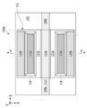
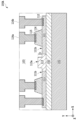
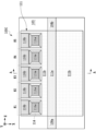
- FIG. 2 is a schematic top view illustrating a configuration example of a light receiver according to the first embodiment. 2 is a cross-sectional view showing the optical receiver shown in FIG. 1 taken along the line AA.
- FIG. 11 is a schematic top view illustrating a configuration example of a light receiver according to a modified example of the first embodiment. 4 is a cross-sectional view showing the optical receiver shown in FIG. 3 taken along the line AA.
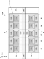
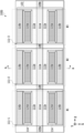
- FIG. 11 is a schematic top view illustrating a configuration example of a light receiver according to a second embodiment. 10 is a graph showing an example of the relationship between the light receiving power by the light absorption circuit according to the second embodiment and the position of the light absorption circuit relative to the light propagation direction.
- FIG. 11 is a schematic top view illustrating a configuration example of a light receiver according to a second embodiment. 10 is a graph showing an example of the relationship between the light receiving power by the light absorption circuit according to the second embodiment and the position of the light absorption circuit relative to the light propagation direction
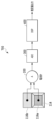
- FIG. 13 is a diagram illustrating an example of a measurement system according to a second embodiment.
- 10 is a flowchart illustrating an example of a procedure for monitoring (or estimating) input optical power according to the second embodiment.
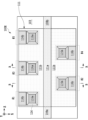
- FIG. 13 is a schematic top view illustrating a configuration example of a light receiver according to a third embodiment.
- 10 is a cross-sectional view showing the optical receiver shown in FIG. 9 taken along the line AA.
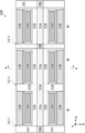
- FIG. 13 is a schematic top view illustrating a configuration example of a light receiver according to a fourth embodiment.
- FIG. 13 is a schematic top view illustrating a configuration example of a light receiver according to a fifth embodiment.
- FIG. 13 is a schematic top view illustrating a configuration example of a light receiver according to a sixth embodiment.
- FIG. 13 is a schematic top view illustrating a configuration example of a light receiver according to a seventh embodiment.
- FIG. 23 is a schematic top view illustrating a configuration example of a light receiver according to an eighth
- the photocurrent generated in a photoreceiver arranged in advance in the optical circuit according to the received optical power may be measured by an ammeter provided outside the optical circuit.
- the photocurrent is determined by (photosensitivity R of the photoreceiver) x (optical power P). Therefore, by knowing the accurate photosensitivity R, it is possible to determine the accurate optical power P for the photocurrent.
- optical sensitivity R there may be individual variations in optical sensitivity R between optical receivers. As a result, errors may occur in the measurement of optical power due to individual variations in optical sensitivity R. In other words, the accuracy of the measurement of optical power may decrease. In addition, it is unrealistic to accurately determine the optical sensitivity R for each optical receiver.
- a method may be considered in which a small portion of the optical power is branched off by an optical branching device and the branched light is received for measurement.
- optical splitter when used to measure optical power, there may be individual variations in the splitting ratio of the optical splitter in addition to the optical sensitivity R of the optical receiver. Therefore, the measurement accuracy of optical power may decrease due to individual variations in the splitting ratio in addition to individual variations in the optical sensitivity R.
- a photoreceiver is used that does not use additional components such as an optical monitor and an optical splitter, but instead uses a second semiconductor to absorb a portion of the light propagating through the first semiconductor (e.g., an optical waveguide) and generates a current according to the amount of light absorbed.
- additional components such as an optical monitor and an optical splitter, but instead uses a second semiconductor to absorb a portion of the light propagating through the first semiconductor (e.g., an optical waveguide) and generates a current according to the amount of light absorbed.
- Such an optical receiver can, for example, suppress the loss of light propagating through the first semiconductor and the deterioration of the accuracy of the optical power monitor.
- a non-limiting example of the second semiconductor that absorbs a portion of the light propagating through the first semiconductor is germanium (Ge).
- germanium Ge
- optical receiver may be appropriately interpreted as "photodetector.”
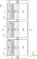
- Fig. 1 is a schematic top view showing a configuration example of the optical receiver 100 according to the first embodiment
- Fig. 2 is a cross-sectional view showing the A-A cross section of the optical receiver shown in Fig. 1.
- the X-axis, the Y-axis, and the Z-axis are added for convenience in explaining the three-dimensional structure of the optical receiver 100.
- the Z axis represents the light guide direction, which corresponds to the length of the receiver 100 when viewed from above
- the X axis represents the direction corresponding to the width of the receiver 100 when viewed from above
- the Y axis represents the direction corresponding to the thickness (or height) of the receiver 100 when viewed from the side or in cross section.
- the directions represented by the X axis, Y axis, and Z axis are the same in the drawings used in the following explanation.
- the optical receiver 100 includes, for example, an SOI (Silicon On Insulator) substrate 101 (hereinafter sometimes abbreviated as "substrate 101"), a first clad layer 102 provided on the upper part of the SOI substrate 101 (e.g., in the positive direction of the Y axis in Figure 2), and a second clad layer 103 provided on the upper part of the first clad layer 102.
- the first clad layer 102 and the second clad layer 103 may be referred to as the lower clad layer 102 and the upper clad layer 103, respectively, to make it easier to understand their relative positional relationship in the Y axis direction (thickness direction).
- the SOI substrate 101 illustratively includes a Si substrate, a Si oxide film, and a surface Si layer.
- the cladding layers 102 and 103 are each formed of a cladding material (e.g., silicon dioxide, SiO2 ) having a lower refractive index than silicon (Si) and germanium (Ge).
- the lower cladding layer 102 may be omitted (e.g., quartz glass).
- a Si layer 111 located on top of the lower cladding layer 102, two Ge layers 114 located on top of the Si layer 111, and a pair of electrodes 116a and 116b for extracting current corresponding to each of the Ge layers 114.
- the material of the electrodes 116a and 116b is not particularly limited as long as it is a material through which a current can flow, but for example, aluminum (Al) may be used as the main material.
- Al aluminum
- the pair of electrodes 116a and 116b may be referred to as the "electrode pair 116.”
- one of the electrode pair 116 is an example of a first electrode and corresponds to a cathode (negative electrode), and the other of the electrode pair 116 is an example of a second electrode and corresponds to an anode (positive electrode).
- One of the electrode pairs 116 (e.g., electrode 116a) is provided on the top of each of the Ge layers 114.
- the other of the electrode pair 116 (e.g., electrode 116b) is provided on the top of the Si layer 111 outside the Ge layer 114 in the width direction (X-axis direction).
- the Si layer 111, the Ge layer 114, and the electrode pair 116 are contained within the upper cladding layer 103, and the gaps between them are filled (or buried) with a cladding material that has a lower refractive index than Si and Ge.
- the surfaces of the two electrode pairs 116 in the thickness direction are, for example, exposed on the upper surface of the upper cladding layer 103.
- the reference numerals are omitted for the set located on the left side of the two sets of Ge layers 114 and electrode pairs 116 located symmetrically in the width direction (X axis direction).
- the Si layer 111 is a non-limiting example of a first semiconductor layer, and is, for example, a p-type Si layer in which Si is doped with p-type impurities, which is an example of a first conductivity type. As shown in FIG. 1, for example, the end in the Z-axis direction of the p-type Si layer 111 (for example, the rib 111a described later) is connected (or coupled) to an optical waveguide 108a that constitutes one of the optical input and optical output, and an optical waveguide 108b that constitutes the other of the optical input and optical output.
- the p-type Si layer 111 is sandwiched between the cladding layers 102 and 103, which have a lower refractive index than the p-type Si layer 111 in the Y-axis direction, and functions as a slab-shaped core layer waveguide that confines the light incident from the optical waveguide 108a (or optical waveguide 108b) inside and guides it to the optical waveguide 108b (or optical waveguide 108a).
- the optical waveguides 108a and 108b may be connected to the p-type Si layer 111 as separate members, or may be formed integrally with the p-type Si layer 111.
- the p-type Si layer 111 of this embodiment has a rib (which may also be called a "ridge") 111a in the center when viewed from above, which extends in the Z-axis direction and has a convex cross-sectional shape that protrudes in the positive direction of the Y-axis when viewed in cross section.
- a rib which may also be called a "ridge” 111a in the center when viewed from above, which extends in the Z-axis direction and has a convex cross-sectional shape that protrudes in the positive direction of the Y-axis when viewed in cross section.
- the p-type Si layer 111 has a first region (hereinafter sometimes referred to as "rib region 111a") having a first thickness in the Y-axis direction that corresponds to the thickness of the rib 111a, and a second region 111b having a second thickness thinner than the first thickness on both sides of the rib 111a in the X-axis direction. Note that in Figure 2, the difference between the first thickness and the second thickness is indicated by "D.”
- the difference D may be set (or designed; the same applies below) to a value on the order of several tens of nanometers to several hundred nanometers, such as 50 nm to 150 nm.
- the width of the rib 111a in the X-axis direction is not particularly limited, but may be set to a value on the order of several hundred nanometers to several micrometers, such as 0.4 ⁇ m to 3 ⁇ m.
- the length of the rib 111a in the Z-axis direction is not particularly limited, but may be set to a value on the order of several micrometers to several tens of micrometers, for example, 5 ⁇ m to 30 ⁇ m.
- the rib-type waveguide 111 having the rib 111a can be formed, for example, by semiconductor deposition technology or microfabrication technology such as photolithography, or both.
- the Si layer 111 having a structure with ribs 111a may be referred to as the "rib-type waveguide 111" or the “convex cross-section Si waveguide 111" for convenience.
- the rib-type waveguide 111 In the rib-type waveguide 111, light with more power propagates while being confined in a concentrated manner in the rib 111a than in the two regions 111b on either side of the rib 111a.
- light propagates while being confined intensively to the rib 111a means that, for example, in the rib-type waveguide 111, the power distribution of the propagating light tends to be higher in the region closer to the rib 111a, and does not mean that the light propagates only to the rib 111a. This point is the same in the following explanations.
- a Ge layer 114 is provided symmetrically on the upper portion of each of the regions 111b on both sides of the rib 111a, for example, on either side of the rib 111a extending in the Z-axis direction.
- Each of the Ge layers 114 is a non-limiting example of a second semiconductor, and for example, extends in the Z-axis direction with a length shorter than the rib-type waveguide 111, and is provided at a fixed interval in the X-axis direction from the edge of the width of the rib 111a.
- the Ge layer 114 may have a mesa shape with inclined sides that define the width in the X-axis direction in the cross-sectional view of FIG. 2.
- the Ge layer 114 does not necessarily have to have a mesa shape, and may have, for example, a convex shape similar to the rib 111a in the cross-sectional view of FIG. 2.
- the Ge layer 114 may be understood as an example of a light absorption section.
- the mesa-shaped Ge layer 114 may be referred to as the "Ge mesa light absorption section 114" for convenience.
- the two Ge layers 114 located on either side of the rib 111a in the width direction (X-axis direction) are formed (or stacked) on the rib-type waveguide 111 by epitaxial growth, as a non-limiting example.
- an n-type Ge region 115 may be formed by doping Ge with n-type impurities, which is an example of a second conductivity type.
- one electrode 116a constituting the electrode pair 116 for extracting the current described above is provided on the upper surface of each n-type Ge region 115 with its lower surface in contact with the upper surface.
- the other electrode 116b constituting the electrode pair 116 is provided on the upper portion of the rib-type waveguide 111, in a region that is outside the Ge layer 114 in the width direction (X-axis direction) with respect to the rib 111a.
- a p++Si electrode portion 112 doped with a high concentration of p-type impurities is provided in the region outside the X-axis direction where the Ge layer 114 of the rib-type waveguide 111 is provided, and an electrode 116b for extracting current is provided so that the lower surface of the electrode 116b contacts the upper surface of the p++Si electrode portion 112.
- electrode 116b may be provided at a position symmetrical in the X-axis direction with rib 111a in between, similar to Ge layer 114 or electrode 116a.
- one or both of p++Si electrode portion 112 and n-type Ge region 115 may be unnecessary, for example, when the current detection sensitivity of electrode pair 116 is within an acceptable range.
- the electrode 116a may be arranged so as to contact the upper part of the p-type Si layer 111 (e.g., the p-type second region 111b) without passing through the p++ Si electrode portion 112.
- the electrode 116b may be arranged so as to contact the upper part of the n-type Ge layer 114 doped with n-type impurities without passing through the n-type Ge region 115.
- the optical receiver 100 having the above-described structure, for example, when light is incident from the optical waveguide 108a to the rib-type waveguide 111, the light propagates through the rib-type waveguide 111 while being confined in a concentrated manner in the rib 111a, and both ends of the optical mode slightly leak out (for example, at a rate of a few percent or less) into the regions 111b on both sides (in the X-axis direction) of the rib 111a.
- the light that seeps into the regions 111b on both sides of the rib 111a is absorbed in the Ge layer 114, which has a higher refractive index than the Si layer 111.
- the Ge layer 114 generates charges according to the power of the absorbed light, and a current according to the generated charges flows through the pair of electrodes 116a and 116b. Therefore, for example, by connecting an ammeter to the pair of electrodes 116, it is possible to partially monitor the optical power propagating through the rib-type waveguide 111.
- the optical receiver 100 is a type of optical receiver that transmits input light without terminating it.
- the Ge mesa light absorption section 114 by suppressing the light absorption rate by the Ge mesa light absorption section 114 to a few percent or less, it is possible to suppress the attenuation (or loss) of the optical power propagating through the rib-type waveguide 111 and output to the output optical waveguide 108b. Therefore, it is possible to realize a low-loss and highly sensitive monitor of the optical power propagating through the rib-type waveguide 111.
- the light absorption rate of the Ge mesa light absorption section 114 can vary depending on, for example, the distance in the X-axis direction between the rib 111a provided on the rib-type waveguide 111 and the Ge mesa light absorption section 114. For example, the shorter the distance in the X-axis direction between the rib 111a and the Ge mesa light absorption section 114, the higher the light absorption rate in the Ge mesa light absorption section 114, and the greater the loss of light propagating through the rib-type waveguide 111 tends to be.
- the distance between the edge that defines the width of the rib 111a in the X-axis direction and the edge of the Ge mesa light absorbing portion 114 that is closer to the rib 111a is set theoretically or experimentally so as to obtain the desired light absorption rate (for example, a few percent or less).
- This setting makes it possible to realize a receiver 100 that can suppress loss of propagating light and deterioration of the accuracy of the optical power monitor.
- the optical absorption rate in the Ge mesa absorption section 114 is set to 5% or less, the distance between the above-mentioned edges is expected to be several ⁇ m to several tens of ⁇ m (e.g., 3 ⁇ m to 30 ⁇ m).
- the relationship between the p-type semiconductor and the n-type semiconductor may be reversed.
- the p-type Si layer (rib-type waveguide) 111 and the p++ Si electrode portion 112 may be replaced with an n-type Si layer and an n++ electrode portion in which Si is doped with n-type impurities, respectively, and the n-type Ge region 115 may be replaced with a p-type Ge region in which Ge is doped with p-type impurities.
- the direction of the current flowing through the pair of electrodes 116a and 116b is reversed compared to the case where the replacement is not performed.
- the fact that the relationship between the p-type semiconductor and the n-type semiconductor may be reversed in this way also applies to the modified examples and other embodiments described later.
- the Ge layer 114 and the electrodes 116a and 116b are arranged symmetrically on both sides of the X-axis direction with respect to the rib 111a extending in the Z-axis direction of the rib-type waveguide 111, but an asymmetric arrangement may also be adopted. Some examples of asymmetric arrangements will be described in other embodiments described later.
- Fig. 3 is a schematic top view showing a configuration example of an optical receiver 100A according to a modified example of the first embodiment
- Fig. 4 is a cross-sectional view showing the A-A cross section of the optical receiver 100A shown in Fig. 3.
- the optical receiver 100A illustrated in FIGS. 3 and 4 differs from the first embodiment in part of the configuration of the Si layer 111, which is a rib-type waveguide, for example, in the material of at least the rib 113a.
- the region of the rib 113a having the first thickness of the Si layer 111 (hereinafter also referred to as the rib region 113a) is a region that is not doped with p-type impurities, unlike the first embodiment.
- a part or all of the region 111b having a second thickness that is thinner than the first thickness of the Si layer 111 is a region doped with p-type impurities, as in the first embodiment.
- the peripheral regions on both sides of the rib region 113a in the width direction (X-axis direction) of the region 111b having the second thickness are also regions that are not doped with p-type impurities.
- the convex region 113 including the rib region 113a is an intrinsic Si region that has a higher refractive index than a region doped with p-type impurities.
- a rib having such a convex region 113 that is not doped with p-type impurities will be referred to as an intrinsic Si rib 113 (or intrinsic Si region 113).
- the width of the intrinsic Si rib 113 in the X-axis direction may be set theoretically or experimentally within a range in which it does not overlap or contact the Ge mesa absorption portion 114 on the second region 111b having the second thickness of the rib-type waveguide 111.
- the intrinsic Si rib 113 in the rib-type waveguide 111 it is possible to suppress undesired light absorption caused by impurity doping more than in the first embodiment. Therefore, compared to the first embodiment, the loss of light propagating through the rib-type waveguide 111 can be further reduced.
- the intrinsic Si rib 113 in the rib-type waveguide 111 shown in this modified example can also be applied to other embodiments described later.
- Fig. 5 is a schematic top view showing a configuration example of an optical receiver 100B according to the second embodiment.
- the optical receiver 100B also includes a plurality (e.g., 5 pairs) of electrode pairs 116 (10 in total for the electrode pairs, 20 in total for the individual electrodes that make up the electrode pairs) corresponding to the individual Ge mesa absorption sections 114 at the top of the rib-type waveguide 111.
- a plurality e.g., 5 pairs
- electrode pairs 116 (10 in total for the electrode pairs, 20 in total for the individual electrodes that make up the electrode pairs) corresponding to the individual Ge mesa absorption sections 114 at the top of the rib-type waveguide 111.
- Ge mesa absorption section 114 and the electrode pair 116 may be the same as those in the first embodiment, or may be changed as appropriate according to the size of the optical receiver 100B (e.g., the substrate 101).
- Figure 5 shows an example in which five Ge mesa absorption sections 114 and electrode pairs 116 are arranged in series in the Z-axis direction in each of the two regions 111b on both sides of the rib 111a, so that the length of each in the Z-axis direction is smaller than that in the first embodiment.
- the set of two Ge mesa light absorption sections 114 arranged symmetrically in the X-axis direction with the rib 111a in between, and the two electrode pairs 116 corresponding to these two Ge mesa light absorption sections 114 may be conveniently referred to as a "light absorption circuit” or "light detection circuit.”
- a light absorption circuit or "light detection circuit.”
- the spacing in the Z-axis direction of the sets of Ge mesa light absorbing sections 114 and electrode pairs 116 may be set, for example, based on the effect of mutual interference between the currents generated in the individual Ge mesa light absorbing sections 114 (hereinafter also referred to as "current crosstalk").
- the spacing in the Z-axis direction may be set to a value within a range in which no current crosstalk occurs, or within an acceptable range in which current crosstalk does occur.
- the arrangement illustrated in FIG. 5 makes it possible to monitor the power of light propagating through the rib-type waveguide 111 at multiple positions or regions in the Z-axis direction (which may be conveniently referred to as a "multipoint monitor").
- the other components of the optical receiver 100B may be the same as or similar to those in the first embodiment.
- the A-A cross section in FIG. 5 (in other words, the layered structure of the optical receiver 100B in the Y-axis direction) may be understood to be the same as the A-A cross section illustrated in FIG. 2 (or FIG. 4).
- the lower cladding layer 102 is laminated on the top of the substrate 101, and the rib-type waveguide 111 is laminated on the top of the lower cladding layer 102.
- a Ge mesa absorption section 114 is provided on the top of the rib-type waveguide 111, and an electrode pair 116 is provided on the top of the Ge mesa absorption section 114 and the rib-type waveguide 111.
- the rib-type waveguide 111 is common to the multiple Ge mesa absorption sections 114 and the multiple electrode pairs 116 that form each of the multiple absorption circuits #1 to #5.
- FIG. 5 only the cut line A-A is shown, focusing on one of the light absorption circuits #1 to #5 (light absorption circuit #3), and the other four sets of light absorption circuits #1, #2, #4, and #5 are omitted from the illustration. It may be understood that the layered structure in the Y-axis direction of each of the other four sets of light absorption circuits #1, #2, #4, and #5 is also the same as that in FIG. 2 (or FIG. 4).
- the optical receiver 100B having the above-described structure, for example, when light is incident from the optical waveguide 108a to the rib-type waveguide 111, the light propagates through the rib-type waveguide 111 while being confined in a concentrated manner in the rib 111a, and both ends of the optical mode leak out slightly (for example, at a rate of a few percent or less) into the regions 111b on both sides (in the X-axis direction) of the rib 111a.
- the light that seeps into the regions 111b on both sides of the rib 111a is absorbed by two Ge mesa light absorption sections 114 arranged symmetrically in the X-axis direction in each of the light absorption circuits #1 to #5. Then, in each Ge mesa light absorption section 114, a charge is generated according to the power of the absorbed light, and a current according to the generated charge flows through the corresponding electrode pair 116.
- the multipoint monitor In the multipoint monitor, a small portion of the light propagating through the rib-type waveguide 111 is absorbed in each of the multiple light absorption circuits #i (i is any of 1 to n), so the power of the propagating light is more likely to attenuate the further back in the propagation direction it moves. Therefore, the amount of light absorption tends to decrease in the light absorption circuits #i located further back in the light propagation direction, and the magnitude of the current flowing through the electrode pair 116 also tends to decrease.
- Fig. 6 is a graph showing an example of the relationship between the optical power received by the optical absorption circuit #i (vertical axis) and the position of the optical absorption circuit #i relative to the optical propagation direction (horizontal axis).
- the horizontal axis in FIG. 6 indicates the position of the light absorption circuit #i in the light propagation direction by the ascending light absorption circuit number (i). In other words, the horizontal axis in FIG. 6 indicates that the larger the light absorption circuit number, the greater the distance in the light propagation direction based on the position where the light enters the first-stage light absorption circuit #1.
- each light absorption circuit #i includes two Ge mesa light absorption sections 114 arranged symmetrically on either side of the rib 111a. Therefore, for example, one of the current values generated by each of the two Ge mesa light absorption sections 114 may be selected as the current value of one light absorption circuit #i, or the average value of the two current values may be determined as the current value of one light absorption circuit #i.
- the "average” may be a simple average or a weighted average.
- a regression line 602 is derived from the received light power derived for each of the multiple light absorption circuits #i, and an intersection point 603 (point plotted as a white circle in FIG. 6) between the regression line 602 and the position of the first-stage light absorption circuit #1 on the graph is determined.
- the optical power on the vertical axis corresponding to the intersection point 603 corresponds to the estimated value (or may be called a predicted value) of the input optical power to the first-stage light absorption circuit #1. Therefore, for example, the estimation accuracy of the input optical power to the optical receiver 100B can be improved.
- FIG. 7 is a diagram showing an example of a measurement system 700 according to the second embodiment.
- the measurement system 700 includes an ammeter 200, an analog-to-digital converter (ADC) 300, and a processor 400. Two or more of the ammeter 200, the ADC 300, and the processor 400 may be provided.
- FIG. 7 shows, by way of example, an example of the connection relationship between the electrode pair 116 and the processor 400 when focusing on one Ge mesa absorption section 114 included in one absorption circuit #i.
- an ammeter 200 is connected to an electrode pair 116 corresponding to one Ge mesa absorption section 114, an analog-to-digital converter (ADC) 300 is connected to the output of the ammeter 200, and a processor 400 is connected to the output of the ADC 300.
- ADC analog-to-digital converter
- the current flowing through the electrode pair 116 is measured by the ammeter 200, and the measured analog current value is AD converted by the ADC 300 to generate a digital current value, which is then input to the processor 400.
- a digital current value for each light absorption circuit #i is obtained and input to the processor 400.
- current measurements for multiple light absorption circuits #i may be performed by repeatedly changing the light absorption circuit #i (electrode pair 116) to which the ammeter 200 is connected one by one.
- a switch (not shown) for switching the connection between the multiple electrode pairs 116 and the ammeter 200 may be provided, and the connection target of the ammeter 200 may be switched by switching control of the switch.
- the switching control of the switch may be performed by, for example, the processor 400.
- the ammeter 200, the ADC 300, and the processor 400 can be shared by multiple light absorption circuits #i, thereby reducing the scale of the measurement system 700.
- current measurements for multiple light absorption circuits #i may be performed, for example, by connecting multiple ammeters 200 individually to each of the electrode pairs 116 of each light absorption circuit #i.
- FIG. 8 is a flowchart showing an example of a procedure for monitoring (or estimating) input optical power according to the second embodiment.
- light is input to the optical receiver 100B (e.g., optical waveguide 108a) (S10).
- the light input to the optical waveguide 108a may be transmitted light from an optical transmitter having a light source, or may be received light from an optical receiver that receives light transmitted through an optical transmission path such as an optical fiber.
- the processor 400 derives a regression line 602 as shown in FIG. 6 based on the digital current values obtained for each light absorption circuit #i (S30). Based on the regression line 602, the processor 400 estimates the optical power input to the first-stage light absorption circuit #1 by, for example, finding the intersection point 603 on the graph shown in FIG. 6 (S40). The processor 400 then outputs the estimated value obtained by the estimation (S50).
- the output destination of the estimated value can be a control circuit that feedback controls the output power of the transmitted light in the optical transmitter, or a control circuit that controls the gain of the amplifier in the optical receiver.
- it can be, but is not limited to, a display device such as a display, a printing device such as a printer, another processor, a storage device or storage medium such as a memory, or a communication line.
- the current value is measured for each electrode pair 116 of the multiple Ge mesa absorption sections 114 arranged in series in the Z-axis direction. Then, in the processor 400, a regression line 602 is derived based on each measured current value, and the input optical power to the optical receiver 100B is estimated based on the regression line 602. Therefore, it is possible to improve the monitoring accuracy while suppressing the loss of light propagating through the rib-type waveguide 111.
- the input optical power to the first-stage light absorption circuit #1 is estimated, but for example, the output optical power of the last light absorption circuit #n may be estimated based on the regression line 602.
- the number of light absorption circuits #i in other words, the number of current measurement points along the direction in which light propagates through the rib-type waveguide 111
- n is not limited to 5 and may be any number that allows the regression line 602 to be derived, for example, n ⁇ 2.
- n the more accurate the regression line 602 is derived, and as a result, the more accurate the estimation of the input optical power is.
- the loss of light propagating through the rib-type waveguide 111 tends to increase.
- the value of n may be appropriately determined based on, for example, the trade-off between the desired estimation accuracy of the input optical power and the tolerable optical loss level.
- the "derivation" of the regression line 602 may be a “calculation” by computing a regression equation, or it may be a “determination” without “calculation”, such as by referring to data in a table format (in other words, by looking up a table).
- the relationship between the light receiving power by the light absorption circuit #i and the position of the light absorption circuit #i relative to the light propagation direction may be approximated by a method different from the method for deriving the regression line 602.
- Fig. 9 is a schematic top view showing a configuration example of a light receiver 100C according to the third embodiment
- Fig. 10 is a cross-sectional view showing a cross section of the light receiver 100C shown in Fig. 9 taken along the line A-A.
- region 111b is a region that is thinner than the thickness of rib 111a in the rib-type waveguide 111.
- the absorption circuit #i includes one Ge mesa absorption section 114 and one electrode pair 116. Therefore, for example, the selection or averaging of two current values obtained from each absorption circuit #i as described in the second embodiment is not necessary in the third embodiment.
- the other components of the receiver 100C may be the same as or similar to those in the first and second embodiments.
- a lower clad layer 102 is laminated on the top of the substrate 101
- a rib-type waveguide 111 is laminated on the top of the lower clad layer 102.
- a Ge mesa absorption section 114 is provided on the top of one of the two regions 111b of the rib-type waveguide 111
- an electrode pair 116 is provided on the top of the Ge mesa absorption section 114 and the rib-type waveguide 111.
- the rib-type waveguide 111 is common to the multiple Ge mesa absorption sections 114 and multiple electrode pairs 116 that form each of the multiple absorption circuits #1 to #5.
- FIG. 9 only the cut line A-A is shown, focusing on one of the light absorption circuits #1 to #5 (light absorption circuit #3), and the other four sets of light absorption circuits #1, #2, #4, and #5 are omitted from the illustration. It may be understood that the layered structure in the Y-axis direction of each of the other four sets of light absorption circuits #1, #2, #4, and #5 is also the same as that in FIG. 10.
- the optical receiver 100C having the above-described structure, for example, when light is incident from the optical waveguide 108a to the rib-type waveguide 111, the light propagates through the rib-type waveguide 111 while being confined in a concentrated manner in the rib 111a, and both ends of the optical mode slightly leak out (for example, at a rate of a few percent or less) into the regions 111b on both sides (in the X-axis direction) of the rib 111a.
- the light that seeps into the regions 111b on both sides of the rib 111a is absorbed by the Ge mesa light absorption section 114 in each of the light absorption circuits #1 to #5. Then, in each of the Ge mesa light absorption sections 114, a charge is generated according to the power of the absorbed light, and a current according to the generated charge flows through the corresponding electrode pair 116.
- a multipoint monitor similar to that of the second embodiment is realized for one region 111b of the rib-type waveguide 111 in which the light absorption circuits #1 to #5 are provided.
- Other operational examples may be understood to be equivalent to those of the second embodiment.
- the multipoint monitor also makes it possible in the third embodiment to derive a regression line 602 based on current values measured at multiple current measurement points in the Z-axis direction, and to estimate the input optical power (or output optical power) based on the derived regression line 602.
- the loss of light propagating through the rib-type waveguide 111 can be reduced more than in the optical receiver 100B according to the second embodiment, in which the Ge mesa absorption portion 114 is disposed in the region 111b on both sides of the rib 111a in the Z-axis direction. Therefore, for example, when the input optical power to the optical receiver 100C is lower than in the second embodiment, it is easier to achieve the desired optical output power.
- the amount of light absorbed by the Ge mesa light absorption section 114 tends to decrease, so the accuracy or sensitivity of the optical power monitor based on current measurement tends to decrease.
- the accuracy or sensitivity of the optical power monitor it is possible to improve the accuracy or sensitivity of the optical power monitor by, for example, increasing the size of the Ge mesa light absorption section 114 or moving the position closer to the rib 111a without changing the number of Ge mesa light absorption sections 114 arranged.
- Fig. 11 is a schematic top view showing a configuration example of a receiver 100D according to the fourth embodiment.
- the receiver 100D shown in Fig. 11 substantially corresponds to a configuration in which a plurality of receivers 100 (see Figs. 1 and 2) shown in the first embodiment are arranged in series in the Z-axis direction (for example, three).
- optical receiver 100D includes multiple optical receivers 100 as components, it may be referred to as a "optical receiver circuit 100D" for convenience.
- cross section taken along the line A-A in FIG. 11 may be understood to be the same as the cross section shown in FIG. 2 (or FIG. 4).
- the optical receiver 100D includes a substrate 101, a lower clad layer 102 provided on the upper part of the substrate 101 in the Y-axis direction, and an upper clad layer 103 provided on the upper part of the lower clad layer 102 in the Y-axis direction.
- rib-type waveguides 111-1 to 111-m are arranged in series in the Z-axis direction above the Y-axis direction of the common lower cladding layer 102.
- the adjacent rib-type waveguides 111-j (e.g., ribs 111a) in the Z-axis direction are connected by optical waveguides 108 provided at the top of the lower cladding layer 102 in the Y-axis direction.
- j represents any one of integers from 1 to m.
- the end of the rib-type waveguide 111-1 in the Z-axis direction that is not connected to the optical waveguide 108 is connected, for example, to the optical waveguide 108a provided at the top of the lower cladding layer 102 in the Y-axis direction.
- the end of the rib-type waveguide 111-3 in the Z-axis direction that is not connected to the optical waveguide 108 is connected, for example, to the optical waveguide 108b provided at the top of the lower cladding layer 102 in the Y-axis direction.
- optical waveguide 108a when light is input to optical waveguide 108a, the input light propagates in the positive direction of the Z axis through rib-type waveguide 111-1, optical waveguide 108, rib-type waveguide 111-2, optical waveguide 108, and rib-type waveguide 111-3 in that order, and is output from optical waveguide 108b. Note that light can also propagate in the reverse direction (negative direction of the Z axis).
- the Ge mesa light-absorbing portion 114 and the electrode pair 116 are arranged symmetrically in the X-axis direction in the regions 111b on both sides of the rib 111a in the X-axis direction, as in the first embodiment.
- the substrate 101, the lower cladding layer 102, and the upper cladding layer 103 are common to the three rib-type waveguides 111-1 to 111-3 and the two sets of Ge mesa absorption sections 114 and electrode pairs 116 that are provided symmetrically in the X-axis direction above the Y-axis direction of each of the rib-type waveguides 111-1 to 111-3.
- the two sets of Ge mesa absorption sections 114 and electrode pairs 116 are provided individually for each of the multiple rib-type waveguides 111-1 to 111-3.
- the accuracy of current measurement for each light absorption circuit #i is improved.
- the accuracy of the derived regression line 602 and the estimation accuracy of the input optical power (or output optical power) based on the regression line 602 are improved.
- FIG. 11 only shows the cutting line A-A focusing on one of the three light absorption circuits #1 to #3 (e.g., light absorption circuit #2), and the other two sets of light absorption circuits #1 and #3 are omitted from the illustration. It may be understood that the layered structure in the Y-axis direction of each of the other two sets of light absorption circuits #1 and #3 is also the same as FIG. 2 (or FIG. 4).
- the receiver structures exemplified in the first embodiment (including the modified examples) to the fourth embodiment described above may be implemented in combination as appropriate. As non-limiting examples of combinations, several variations are shown below in Figs. 12 to 15 as the fifth to eighth embodiments.
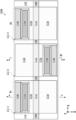
- FIG. 12 is a schematic top view showing a configuration example of a photodetector 100E according to the fifth embodiment.
- the photodetector 100E shown in Fig. 12 has a configuration in which, for example, a plurality of sets (e.g., five light absorption circuits #i) of Ge mesa light absorption portions 114 and electrode pairs 116 are alternately arranged at different positions in the Z-axis direction in one and the other of two regions 111b on both sides of the rib 111a in the X-axis direction.
- sets e.g., five light absorption circuits #i
- the configuration illustrated in FIG. 12 may be understood to correspond to a configuration in which a portion of the multiple light absorption circuits #i arranged in series in the Z-axis direction in each of the regions 111b on both sides of the X-axis direction, sandwiching the rib 111a in the configuration in FIG. 5, is thinned out.
- the cross sections of each of the five light absorption circuits #i may be understood to correspond, for example, to the cross sections shown in FIG. 10 of the third embodiment.
- FIG. 13 is a schematic top view showing a configuration example of a photoreceiver 100F according to the sixth embodiment.
- the photoreceiver 100F shown in Fig. 13 has a configuration in which some of the multiple rib-type waveguides 111-j are common to multiple light-absorption circuits #j in the configuration shown in Fig. 11 of the fourth embodiment.
- the optical receiver 100F has two rib-type waveguides 111-1 and 111-2 on the upper part of the lower cladding layer 102, and one of the rib-type waveguides 111-1 is common to the two light absorption circuits #1 and #2.
- the other rib-type waveguide 111-2 has one light absorption circuit #3, as in the example shown in FIG. 11.
- the cross section of each light absorption circuit #i (for example, the cross section taken along the line A-A in FIG. 13) may be understood to correspond to the cross section shown in FIG. 10 of the third embodiment, for example.
- This arrangement makes it easy to selectively set positions or areas in the receiver 100F (e.g., the upper part of the substrate 101) that can reduce current crosstalk in the Z-axis direction, and is therefore expected to improve the degree of freedom in the design of the receiver 100F.
- FIG. 14 is a schematic top view showing a configuration example of a receiver 100G according to a seventh embodiment.
- the receiver 100G shown in Fig. 14 corresponds to a combination of the fourth embodiment (Fig. 11) and the third embodiment (Fig. 9).
- This arrangement can suppress current crosstalk between the light absorption circuits #i and reduce the loss of light propagating through the rib-type waveguide 111.
- FIG. 15 is a schematic top view showing a configuration example of a receiver 100H according to an eighth embodiment.
- the same effect as in the fourth embodiment can be obtained, and in addition, as in the fifth embodiment, it is easy to ensure a spacing margin between the light absorption circuits that is sufficient to minimize current crosstalk in the Z-axis direction, which is expected to improve measurement accuracy and reduce the size of the receiver.
- a portion of the light propagating through the rib-type waveguide 111 and seeping out from the rib 111a is absorbed by the Ge layer 114, and the flow of charges (i.e., current) generated according to the power of the light absorbed by the Ge layer 114 is measured.
- the configuration illustrated in FIG. 9, which has a smaller number of light absorption circuits #i may be preferentially applied to the optical receiver configuration applied to the optical transmitter.
- the configuration illustrated in FIG. 5, which has a larger number of light absorption circuits #i may be applied to the optical receiver.
- the rib 111a extending in the Z-axis direction is disposed at the center in the width direction (X-axis direction) of the Si layer 111, which is an example of the first semiconductor.
- the rib 111a may be disposed at a position shifted in the X-axis direction from the center in the width direction (X-axis direction) of the Si layer 111.
- the size or number of the light absorption circuit #i (Ge mesa light absorption section 114 and electrode pair 116) to be disposed may be set according to each area.
- drawings used in this disclosure show an example in which multiple Ge mesa absorption sections 114 (and electrode pairs 116) are aligned at equal intervals or symmetrically in the Z-axis direction or X-axis direction.
- multiple Ge mesa absorption sections 114 may be arranged at unequal intervals or asymmetrically in the Z-axis direction or X-axis direction.
- the sizes of multiple Ge mesa absorption sections 114 or the distances between them in the X-axis direction relative to rib 111a (or 113a) may be the same or may be partially or completely different.
- each Ge mesa light absorption section 114 when multiple Ge mesa light absorption sections 114 are arranged in series in the Z-axis direction, the size of each Ge mesa light absorption section 114 may be set so that the amount of light absorption increases as the Ge mesa light absorption section 114 is located downstream in the positive (or negative) direction of the Z-axis. Additionally or alternatively, when multiple Ge mesa light absorption sections 114 are arranged in series in the Z-axis direction, the individual positions may be set so that the Ge mesa light absorption section 114 located downstream in the positive (or negative) direction of the Z-axis is closer to the rib 111a in the X-axis direction.
- the current values measured at multiple current measurement points in the Z-axis direction tend to fall within a certain range, unlike the graph illustrated in FIG. 6. Therefore, instead of deriving the regression line 602, it becomes possible to estimate the optical input power (or optical output power) by, for example, averaging the measured current values obtained by the multipoint monitor.
- the optical input power or optical output power
- stacked used in the present disclosure may be understood to include not only an embodiment in which two layers are directly overlapped, but also an embodiment in which one or more other layers are interposed between the two layers.
- a receiver has a structure different from the stacked structure exemplified in the present disclosure, it does not deviate from the spirit and scope of the present disclosure as long as the structure is such that a part of the light propagating through the rib-type waveguide 111, which is an example of a first semiconductor, can be absorbed by the Ge layer 114, which is an example of a second semiconductor.
- any reference to an element followed by a designation such as “first", “second" does not limit the quantity or order of those elements. These designations are merely used as a convenient way to distinguish between two or more elements. For example, a reference to a first and a second element does not imply that only two elements may be employed, nor does it imply that the first element must precede the second element in any physical quantity.
- circuit and “portion” may be interpreted as mutually interchangeable, or may be interpreted as other terms such as “means” or “device”, as appropriate.
- detection may be interpreted as other terms such as “measurement”, “instrumentation”, “observation”, or “monitor”, as appropriate, depending on the context.
- region may be interpreted as “portion”, as appropriate.
- This disclosure is useful for technologies that use optical circuits, such as optical communication systems or optical information processing systems.
- Photodetector 101 SOI substrate 102 Lower cladding layer 103 Upper cladding layer 108, 108a, 108b Optical waveguide 111, 111-1 to 111-3 Silicon (Si) layer 111a First region (rib) 111b second region 112 p++ Si electrode portion 113 convex region (intrinsic Si region) 114 Germanium (Ge) layer 115 n-type Ge region 116a, 116b Electrodes 200 Ammeter 300 Analog-to-digital converter (ADC) 400 Processor 700 Measurement system
Landscapes
- Light Receiving Elements (AREA)
Abstract
受光器(100)は、基板(101)、第1の半導体層(111)、第2の半導体層(114)、第1の電極(116b)、第2の電極(116a)、および、第1の半導体層(111)に接続された光導波路を備える。第1の半導体層(111)は、第1の厚みを有する第1の領域(111a)と、第1の厚みよりも薄い第2の厚みを有する第2の領域(111b)とを有する。第2の半導体層(114)は、第1の半導体層(111)よりも屈折率が高く、第2の領域(111b)の上部に設けられる。第1の電極(116b)は、第1の領域(111a)に対して第2の半導体層(114)よりも外側の位置に設けられ、第2の電極(116a)は、第2の半導体層(114)の上部に設けられる。
Description
本開示は、受光器、受光回路、および、モニタ方法に関する。
近年の光通信の普及に伴い、光通信装置の低コスト化が求められている。この要求に対し、例えば、光通信装置を構成する光回路を、シリコンウエハなどの大口径ウエハ上に、シリコンフォトニクスのような微小光回路技術を用いて形成する技術がある。
シリコンフォトニクスのような光回路を制御する場合、光回路内の特定のポイントにおける光パワー(例えば、絶対値)を正確に検出することで、光回路の動作を最適化することが可能である。
また、光回路を用いた光モジュールを製造する場合においても、正確な光パワー検出は有用である。例えば、正確な光パワー検出は、製造される光モジュールが所期の性能または動作条件を満たしているかといった、試験的な工程に役立ち得る。
本開示の非限定的な目的の1つは、受光する光を低損失で高精度にモニタすることが可能な受光器を提供することにある。
本開示の一態様に係る受光器は、基板と、前記基板の上部に設けられ、第1の厚みを有する第1の領域と、前記第1の厚みよりも薄い第2の厚みを有する第2の領域とを有する第1の半導体層と、前記第2の領域の上部に設けられ、前記第1の半導体層よりも屈折率の高い第2の半導体層と、前記第2の領域の上部において前記第1の領域に対して前記第2の半導体層よりも外側の位置に設けられた第1の電極と、前記第2の半導体層の上部に設けられた第2の電極と、前記第1の半導体層に接続された光導波路と、を備える。
以下、図面を参照しながら実施形態について詳細に説明する。なお、冗長な説明を避けて説明の簡易化および明瞭化を図る目的で、図面において、同一の番号を付した要素または部分は、特に断らない限り、同一または同様の要素または部分を指す。
[概要]
光回路内の光パワーを外部から観測するために、光回路内に予め配置された受光器において受光パワーに応じて生じる光電流を、光回路の外部に設けられた電流計によって測定することがある。光電流は、(受光器の光感度R)×(光パワーP)によって決定される。そのため、正確な光感度Rを把握しておくことで、光電流に対する正確な光パワーPを決定できる。
光回路内の光パワーを外部から観測するために、光回路内に予め配置された受光器において受光パワーに応じて生じる光電流を、光回路の外部に設けられた電流計によって測定することがある。光電流は、(受光器の光感度R)×(光パワーP)によって決定される。そのため、正確な光感度Rを把握しておくことで、光電流に対する正確な光パワーPを決定できる。
しかしながら、光感度Rには、受光器ごとの個体ばらつきが存在し得る。そのため、光感度Rの個体ばらつきに起因して、光パワーの測定に誤差が生じ得る。換言すると、光パワーの測定精度が低下し得る。また、受光器ごとに正確な光感度Rを把握しておくことは非現実的である。
また、通常の受光器では、例えば、光吸収量が大き過ぎるために、光パワーを可能な限り減衰させずに光パワーの測定を実施したい、といった要望または需要に応えることが難しい場合がある。このような事態または事象を回避するために、例えば、光パワーの僅かな一部分を光分岐器によって分岐し、その分岐光を測定用に受光する方法が検討され得る。
しかしながら、光パワー測定に光分岐器を用いる場合、受光器の光感度Rに加えて光分岐器の分岐比にも個体ばらつきが存在し得る。そのため、光感度Rの個体ばらつきに加えて分岐比の個体ばらつきによっても、光パワーの測定精度が低下し得る。
以下に説明する本開示の例示的な実施形態では、光モニタおよび光分岐器といった追加の部品を用いずに、第1の半導体(例えば、光導波路)を伝搬する光の一部を第2の半導体によって吸収し、その光吸収量に応じた電流を発生する構造の受光器を用いる。
このような受光器によれば、例えば、第1の半導体を伝搬する光の損失と光パワーモニタの精度低下とを抑制可能である。第1の半導体を伝搬する光の一部を吸収する第2の半導体の非限定的な例としては、ゲルマニウム(Ge)が挙げられる。以下、Geを吸光部に用いた構造の受光器について幾つかの例示的な実施形態を説明する。なお、以下の説明において、「受光器」は、「光検出器」に適宜に読み替えられてもよい。
[第1の実施形態]
図1は、第1の実施形態に係る受光器100の構成例を示す模式的な上面図であり、図2は、図1に例示した受光器のA-A断面を示す断面図である。図1および図2において、X軸、Y軸、およびZ軸は、受光器100の3次元的な構造を説明するために便宜的に付記されている。
図1は、第1の実施形態に係る受光器100の構成例を示す模式的な上面図であり、図2は、図1に例示した受光器のA-A断面を示す断面図である。図1および図2において、X軸、Y軸、およびZ軸は、受光器100の3次元的な構造を説明するために便宜的に付記されている。
Z軸は、光の導波方向であって、上面視における受光器100の長さに対応する方向を表し、X軸は、上面視における受光器100の幅に対応する方向を表し、Y軸は、側面視または断面視における受光器100の厚さ(または高さ)に対応する方向を表す。このようなX軸、Y軸およびZ軸が表す方向は、以降の説明において使用する図面においても同様である。
図1および図2に示すように、受光器100は、例えば、SOI(Silicon On Insulator)基板101(以下、「基板101」と略記することがある)と、SOI基板101の上部(例えば図2のY軸の正方向)に設けられた第1のクラッド層102と、第1のクラッド層102の上部に設けられた第2のクラッド層103と、を備える。第1のクラッド層102および第2のクラッド層103は、Y軸の方向(厚み方向)における相対的な位置関係を理解し易いように、それぞれ、下部クラッド層102および上部クラッド層103と称されてもよい。
SOI基板101は、例示的に、Si基板、Si酸化膜、及び表面Si層を備える。クラッド層102およびクラッド層103のそれぞれは、例えば、シリコン(Si)及びゲルマニウム(Ge)よりも屈折率の低いクラッド材料(例えば、二酸化ケイ素,SiO2)によって形成される。なお、基板101の材質によっては下部クラッド層102を省略できることがある(例えば、石英ガラス)。
また、図2に示すように、上部クラッド層103の内部には、下部クラッド層102の上部に位置するSi層111と、Si層111の上部に位置する2つのGe層114と、Ge層114のそれぞれに対応した電流取り出し用の電極116aおよび116bの対と、が設けられる。
電極116aおよび116bの材料は、電流が流れる材料であれば特に限定されないが、例示的に、アルミニウム(Al)が主な材料に使用されてよい。なお、電極116aおよび116bの対を便宜的に「電極対116」と表記することがある。
例示的に、電極対116の一方は、第1の電極の例であってカソード極(-極)に相当し、電極対116の他方は、第2の電極の例であってアノード極(+極)に相当する。
電極対116の一方(例えば、電極116a)は、Ge層114それぞれの上部に設けられる。電極対116の他方(例えば、電極116b)は、幅方向(X軸方向)においてGe層114よりも外側のSi層111の上部に設けられる。
別言すると、下部クラッド層102の上部において、Si層111、Ge層114、電極対116は、上部クラッド層103に内包され、それぞれの間隙が、Si及びGeよりも屈折率の低いクラッド材料によって満たされて(または、埋められて)いる。
なお、2組の電極対116それぞれの厚み方向(Y軸の正方向)の表面は、例示的に、上部クラッド層103の上面に露出している。また、図2において、幅方向(X軸方向)の左右対称に位置する2つのGe層114および電極対116のセットのうちの左側に位置するセットについては、図面における見やすさのために、符号の明示を省略している。
Si層111は、第1の半導体層の非限定的な例であり、例えば、第1導電型の例であるp型の不純物をSiにドーピングしたp型Si層である。p型Si層111(例えば、後述するリブ111a)のZ軸方向の端部には、例えば図1に示すように、光入力および光出力の一方を成す光導波路108aと、光入力および光出力の他方を成す光導波路108bと、が接続(または結合)される。
p型Si層111は、Y軸方向においてp型Si層111よりも屈折率の低いクラッド層102およびクラッド層103によって挟まれるので、光導波路108a(または、光導波路108b)から入射した光を内部に閉じ込めながら光導波路108b(または、光導波路108a)へ導くスラブ状のコア層導波路として機能する。なお、光導波路108aおよび108bの一方または双方は、個別の部材としてp型Si層111に接続されてもよいし、p型Si層111と一体的に形成されてもよい。
ここで、本実施形態のp型Si層111は、図1および図2に例示するように、上面視における中央部に、Z軸方向に延在し、かつ、断面視においてY軸の正方向に突出した凸型断面形状を有するリブ(または「リッジ」と称してもよい)111aを有する。
例えば、p型Si層111は、Y軸方向においてリブ111aの厚みに相当する第1の厚みを有する第1の領域(以下「リブ領域111a」と表記することがある)と、リブ111aを挟んだX軸方向の両側において第1の厚みよりも薄い第2の厚みを有する第2の領域111bと、を有する。なお、図2には、第1の厚みと第2の厚みとの差分が「D」によって示される。
差分Dは、非限定的な一例として、50nm~150nmといった数十nm~百数十nmのオーダの数値に設定(または設計。以下において同じ)されてよい。リブ111aのX軸方向の幅は、特に限定されないが、例えば0.4μm~3μmといった、数百ナノメートル~数マイクロメートルのオーダの数値に設定されてよい。
リブ111aのZ軸方向の長さは、特に限定されないが、例えば5μm~30μmといった、数マイクロメートル~数十マイクロメートルのオーダの数値に設定されてよい。なお、リブ111aを有するリブ型導波路111は、例示的に、半導体の堆積技術またはフォトリソグラフィのような微細加工技術、またはその双方によって形成可能である。
以下、リブ111aを有する構造のSi層111を、便宜的に、「リブ型導波路111」または「凸型断面Si導波路111」と称することがある。リブ型導波路111においては、リブ111aを挟んだ両側の2つの領域111bよりもリブ111aに、より多くのパワーの光が集中的に閉じ込められながら伝搬する。
ここで、「リブ111aに光が集中的に閉じ込められながら伝搬する」とは、例えば、リブ型導波路111において、リブ111aに近い領域ほど伝搬光のパワー分布が高い傾向にあることを意味し、リブ111aのみに光が伝搬することを意味しない。この点は、以降の説明においても同じである。
リブ111aを挟んだ両側の領域111bそれぞれの上部には、Ge層114が、例えば、Z軸方向に延在するリブ111aを挟んで対称に設けられる。Ge層114のそれぞれは、第2の半導体の非限定的な例であり、例えば、リブ型導波路111よりも短い長さでZ軸方向に延在し、リブ111aの幅の縁からX軸方向に一定の間隔を空けて設けられる。
Ge層114は、非限定的な例として、図2の断面視において、X軸方向の幅を規定する側面が傾斜したメサ形状を有してよい。ただし、Ge層114は、必ずしもメサ形状でなくてもよく、例えば、図2の断面視において、リブ111aと同じような凸形状を有していてもよい。
Geの屈折率はSiの屈折率よりも高いため、Si導波路であるリブ型導波路111を伝搬する光のうち、リブ111aに閉じ込めきれずに幅方向(X軸方向)両側の領域111bへ僅かに染み出した光(または、漏れ出した光)が、Ge層114に吸収される。したがって、Ge層114は、吸光部の例と理解されてよい。そのため、以下の説明において、メサ形状を有するGe層114を便宜的に「Geメサ吸光部114」と表記することがある。
リブ111aを挟んで幅方向(X軸方向)両側に位置する2つのGe層114のそれぞれは、非限定的な例として、エピタキシャル成長によってリブ型導波路111上に形成(または積層)される。Ge層114それぞれの上部には、例えば図2に示すように、Geに第2導電型の例であるn型の不純物をドーピングしたn型Ge領域115が形成されてよい。
図2を参照して上述したように、n型Ge領域115それぞれの上面に、上述した電流取り出し用の電極対116を成す一方の電極116aがその下面を接して設けられる。また、電極対116を成す他方の電極116bが、リブ型導波路111の上部であってリブ111aに対してGe層114よりも幅方向(X軸方向)外側の領域に設けられる。
例えば、リブ型導波路111のGe層114が設けられたX軸方向外側の領域に、p型不純物を高濃度にドーピングしたp++Si電極部112が設けられ、このp++Si電極部112の上面に、電流取り出し用の電極116bの下面が接するようにして電極116bが設けられる。
なお、電極116bは、例示的に、Ge層114または電極116aと同様に、リブ111aを挟んでX軸方向に対称な位置に設けられてよい。また、p++Si電極部112およびn型Ge領域115の一方または双方は、例えば、電極対116による電流検出感度が許容範囲内である場合に、不要としてもよい。
例えば、電極116aは、p++Si電極部112を介さずに、p型Si層111(例えば、p型の第2の領域111b)の上部に接するように配置されてよい。また、電極116bは、例えば、n型Ge領域115を介さずに、n型の不純物がドーピングされたn型のGe層114の上部に接するように配置されてよい。
このように、p++Si電極部112およびn型Ge領域115の一方または双方を不要としてもよい場合があることは、以降の説明においても同様である。
(動作例)
上述した構造を有する受光器100において、例えば、光導波路108aからリブ型導波路111に光が入射されると、リブ111aに光が集中的に閉じ込められながらリブ型導波路111を伝搬し、光モードの両端が僅かに(例えば、数%以下の割合で)リブ111aの両側(X軸方向)の領域111bに染み出す。
上述した構造を有する受光器100において、例えば、光導波路108aからリブ型導波路111に光が入射されると、リブ111aに光が集中的に閉じ込められながらリブ型導波路111を伝搬し、光モードの両端が僅かに(例えば、数%以下の割合で)リブ111aの両側(X軸方向)の領域111bに染み出す。
リブ111aの両側の領域111bに染み出した光は、Si層111よりも屈折率の高いGe層114において吸収される。Ge層114は、吸収した光のパワーに応じた電荷を発生し、発生した電荷に応じた電流が電極116aおよび116bの対に流れる。したがって、例えば、電極対116に電流計を接続することで、リブ型導波路111を伝搬する光パワーを部分的にモニタすることが可能である。
なお、Ge層114で吸収されなかった大部分の光パワーは、出力側の光導波路108bに伝搬して受光器100から出力される。別言すると、受光器100は、入力光を終端せずに透過するタイプの受光器である。
ここで、Geメサ吸光部114による光吸収率を数%以下に抑えることで、リブ型導波路111を伝搬して出力側の光導波路108bへ出力される光パワーの減衰(または損失)を抑制することが可能である。したがって、リブ型導波路111を伝搬する光パワーの低損失かつ高感度なモニタを実現可能である。
Geメサ吸光部114による光吸収率は、例えば、リブ型導波路111に設けられるリブ111aとGeメサ吸光部114とのX軸方向の間隔に依存して変化し得る。例えば、リブ111aおよびGeメサ吸光部114のX軸方向の間隔が短いほど、Geメサ吸光部114での光吸収率が大きくなり、リブ型導波路111を伝搬する光の損失が大きくなる傾向にある。
したがって、例えば、リブ111aのX軸方向の幅を規定する縁と、Geメサ吸光部114のリブ111aに近い側の縁との間の距離を、所期の光吸収率(例えば、数%以下)が得られるように理論的または実験的に設定する。
このような設定により、伝搬光の損失と光パワーモニタの精度低下とを抑制可能な受光器100を実現できる。非限定的な例として、Geメサ吸光部114での光吸収率を5%以下とする場合、上述した縁どうしの間の距離は、数μm~数十μm(例えば、3μm~30μm)程度が想定される。
なお、上述した実施形態において、p型半導体とn型半導体との関係(別言すると、第1導電型と第2導電型との関係)は、逆であってもよい。例えば、p型Si層(リブ型導波路)111およびp++Si電極部112は、それぞれ、Siにn型の不純物をドーピングしたn型Si層およびn++電極部に置換されてよく、かつ、n型Ge領域115は、Geにp型の不純物をドーピングしたp型Ge領域に置換されてよい。この場合、一対の電極116aおよび116bを流れる電流の向きが、置換しない場合に対して逆方向になる。このようにp型半導体とn型半導体との関係が逆でもよいことは、後述する変形例および他の実施形態についても同様にあてはまる。
また、上述した実施形態においては、Ge層114、電極116aおよび116bが、リブ型導波路111のZ軸方向に延在するリブ111aに対してX軸方向両側に対称に配置される例を示したが、非対称な配置が採用されてもよい。非対称な配置の幾つかの例については、後述する他の実施形態において説明する。
[変形例]
次に、図3および図4を参照して、上述した第1の実施形態の変形例について説明する。図3は、第1の実施形態の変形例に係る受光器100Aの構成例を示す模式的な上面図であり、図4は、図3に例示した受光器100AのA-A断面を示す断面図である。
次に、図3および図4を参照して、上述した第1の実施形態の変形例について説明する。図3は、第1の実施形態の変形例に係る受光器100Aの構成例を示す模式的な上面図であり、図4は、図3に例示した受光器100AのA-A断面を示す断面図である。
図3および図4に示す受光器100Aは、図1および図2に例示した受光器100に比して、リブ型導波路であるSi層111の構成の一部、例えば、少なくともリブ113aの材料が第1の実施形態とは異なる。
図3および図4に非限定的な例を示すように、変形例に係る受光器100Aにおいて、Si層111の第1の厚みを有するリブ113aの領域(以下、リブ領域113aとも表記する)は、第1の実施形態とは異なり、p型の不純物がドーピングされない領域である。
一方、Si層111の第1の厚みよりも薄い第2の厚みを有する領域111bの一部または全部は、第1の実施形態と同様に、p型の不純物がドーピングされた領域である。ただし、図4に示すように、本変形例においては、第2の厚みを有する領域111bのうちリブ領域113aの幅方向(X軸方向)両側の周辺領域についても、p型不純物がドーピングされない領域である。
図4の断面視において、リブ領域113aを含む凸状領域113は、p型不純物がドーピングされた領域よりも高い屈折率を有する真性Si領域である。以下、このようにp型の不純物がドーピングされない凸状領域113を有するリブを、便宜的に、真性Siリブ113(または真性Si領域113)と表記する。
真性Siリブ113のX軸方向の幅は、リブ型導波路111の第2の厚みを有する第2の領域111b上において、Geメサ吸光部114に重ならず、かつ、接しない範囲で理論的または実験的に設定されてよい。
このように、リブ型導波路111において真性Siリブ113を設けることで、不純物ドーピングによって生じる望まれない光吸収を第1の実施形態よりも抑制することが可能である。したがって、第1の実施形態に比して、リブ型導波路111を伝搬する光の損失をより低減できる。
なお、本変形例において示したリブ型導波路111における真性Siリブ113は、後述する他の実施形態においても同様に適用可能である。
[第2の実施形態]
次に、図5から図8を参照して、第2の実施形態について説明する。図5は、第2の実施形態に係る受光器100Bの構成例を示す模式的な上面図である。図5に示すように、受光器100Bは、リブ111aを挟んだ両側のリブ型導波路111上の第2の領域111bのそれぞれに、Z軸方向に直列に並べて配置された複数(例えば、5つ)のGeメサ吸光部114(合計で5×2=10個)を備える。
次に、図5から図8を参照して、第2の実施形態について説明する。図5は、第2の実施形態に係る受光器100Bの構成例を示す模式的な上面図である。図5に示すように、受光器100Bは、リブ111aを挟んだ両側のリブ型導波路111上の第2の領域111bのそれぞれに、Z軸方向に直列に並べて配置された複数(例えば、5つ)のGeメサ吸光部114(合計で5×2=10個)を備える。
また、受光器100Bは、リブ型導波路111の上部において、個々のGeメサ吸光部114に対応した複数(例えば、5組)の電極対116(電極対として合計で10個、電極対を成す個々の電極として合計で20個)と、を備える。
Geメサ吸光部114および電極対116の材料、形状またはサイズといった種々のパラメータは、例えば、第1の実施形態と同じであってもよいし、受光器100B(例えば、基板101)のサイズに応じて適宜に変更されてもよい。図5には、リブ111a両側の2つの領域111bの1つあたりに5つのGeメサ吸光部114および電極対116がZ軸方向に直列に配置されるため、それぞれのZ軸方向の長さが第1の実施形態よりも小さい例が示される。
なお、図5において、リブ111aを挟んでX軸方向に対称に配置された2つのGeメサ吸光部114と、これら2つのGeメサ吸光部114に対応する2つの電極対116とのセットは、便宜的に「吸光回路」または「光検出回路」と称されてよい。図5の例では、2以上の整数を「n」で表した場合に、n=1~5の5組の吸光回路#1~#5が、リブ111aの延在するZ軸方向に直列に配置される。
Geメサ吸光部114および電極対116のセットのZ軸方向の配置間隔は、例えば、個々のGeメサ吸光部114において生じる電流が相互に干渉する影響(以下「電流クロストーク」とも称する)に基づいて設定されてよい。例えば、Z軸方向の配置間隔は、電流クロストークが生じない範囲の値、または電流クロストークが生じても許容可能な範囲の値に設定されてよい。
このように電流クロストークに基づいてZ軸方向の配置間隔を最適化することで、例えば、受光器100Bのサイズ低減、または、1つあたりの受光器100Bに搭載されるGeメサ吸光部114の密度が増加することによる入力光パワーの推定精度(後述)の向上を図ることが可能である。入力光パワーの推定に関しては、図6から図8を参照して詳細を後述する。
図5に例示したような配置により、リブ型導波路111を伝搬する光のパワーをZ軸方向の複数の位置または領域においてモニタ(便宜的に「マルチポイントモニタ」と称してもよい)することが可能である。その他の受光器100Bにおける構成要素は、第1実施形態と同一または同様でよい。例えば、図5におけるA-A断面(別言すると、受光器100BのY軸方向の積層構造)は、図2(または図4)に例示したA-A断面と同じであると理解されてよい。
例えば、基板101の上部に下部クラッド層102が積層され、下部クラッド層102の上部にリブ型導波路111が積層される。そして、リブ型導波路111の上部にGeメサ吸光部114が設けられ、Geメサ吸光部114およびリブ型導波路111の上部に電極対116が設けられる。ただし、第2の実施形態において、リブ型導波路111は、複数の吸光回路#1~#5のそれぞれを成す複数のGeメサ吸光部114および複数の電極対116に共通である。
図5には、吸光回路#1~#5のうちの1つ(吸光回路#3)に着目した切断線A-Aのみが示され、他の4組の吸光回路#1、#2、#4、#5については図示が省略されている。他の4組の吸光回路#1、#2、#4、#5のそれぞれについても、Y軸方向の積層構造は図2(または図4)と同じであると理解されてよい。
上述した構造を有する受光器100Bでは、例えば、光導波路108aからリブ型導波路111に光が入射されると、リブ111aに光が集中的に閉じ込められながらリブ型導波路111を伝搬し、光モードの両端が僅かに(例えば、数%以下の割合で)リブ111aの両側(X軸方向)の領域111bに染み出す。
リブ111aの両側の領域111bに染み出した光は、吸光回路#1~#5のそれぞれにおいて、X軸方向に対称な配置の2つのGeメサ吸光部114によって吸収される。そして、個々のGeメサ吸光部114において、吸収した光のパワーに応じて電荷が発生し、発生した電荷に応じた電流が、対応する電極対116に流れる。
ここで、マルチポイントモニタでは、リブ型導波路111を伝搬する光の僅かな一部が複数の吸光回路#i(iは1~nの何れか)のそれぞれにおいて吸収されるため、伝搬光のパワーは、伝搬方向の後段に進むほど減衰し易い。したがって、光の伝搬方向に対して後段に位置する吸光回路#iほど吸光量が減少する傾向になるため、電極対116に流れる電流の大きさも小さくなる傾向にある。
なお、各吸光回路#iのGeメサ吸光部114において吸収されなかった大部分の光パワーは、出力側の光導波路108bに伝搬して出力される。
(モニタ方法)
次に、上述したマルチポイントモニタにおける光吸収量(または電流値)の減少傾向を利用して受光器100Bに対する入力光パワーを推定する方法について、図6から図8を参照して説明する。図6は、吸光回路#iによる受光パワー(縦軸)と、光の伝搬方向に対する吸光回路#iの位置(横軸)との関係の例を示すグラフである。
次に、上述したマルチポイントモニタにおける光吸収量(または電流値)の減少傾向を利用して受光器100Bに対する入力光パワーを推定する方法について、図6から図8を参照して説明する。図6は、吸光回路#iによる受光パワー(縦軸)と、光の伝搬方向に対する吸光回路#iの位置(横軸)との関係の例を示すグラフである。
なお、図6の横軸は、光の伝搬方向に対する吸光回路#iの位置を昇順の吸光回路番号(i)によって表す。別言すると、図6の横軸は、吸光回路番号が大きいほど初段の吸光回路#1に光が入射する位置を基準にした光の伝搬方向への距離が大きいことを表す。
図6において黒点601でプロットしたように、個々の吸光回路#iにおいて生じた電流値を基に個々の吸光回路#iによる受光パワーが導出される。なお、1つの吸光回路#iには、既述のとおり、リブ111aを挟んで対称に配置された2つのGeメサ吸光部114が含まれる。そのため、例えば、2つのGeメサ吸光部114のそれぞれによって生じる電流値の一方が、1つの吸光回路#iの電流値として選択されてもよいし、2つの電流値の平均値が、1つの吸光回路#iの電流値として決定されてもよい。「平均」は、単純平均であってもよいし、加重平均であってもよい。
そして、例えば、複数の吸光回路#iのそれぞれについて導出された受光パワーから回帰直線602を導出し、回帰直線602と初段の吸光回路#1の位置とのグラフ上での交点(図6において白丸でプロットした点)603を求める。交点603に対応する縦軸の光パワーが、初段の吸光回路#1に対する入力光パワーの推定値(または予測値と称してもよい)に相当する。したがって、例えば、受光器100Bに対する入力光パワーの推定精度を高めることができる。
上述した回帰直線の導出および回帰直線に基づく入力光パワーの推定には、例えば図7に模式的に示すように、デジタルシグナルプロセッサ(DSP)のような演算処理能力を有するプロセッサ400が用いられてよい。図7は、第2の実施形態に係る測定システム700の例を示す図である。
測定システム700は、電流計200と、アナログ-デジタル変換器(ADC)300と、プロセッサ400と、を備える。電流計200、ADC300およびプロセッサ400の一部または全部は、2つ以上備えられていてもよい。図7には、例示的に、1つの吸光回路#iに含まれる1つのGeメサ吸光部114に着目した場合の電極対116とプロセッサ400との接続関係の例が示される。
図7に示すように、1つのGeメサ吸光部114に対応する電極対116に、電流計200が接続され、電流計200の出力にアナログ-デジタル変換器(ADC)300が接続され、ADC300の出力にプロセッサ400が接続される。
電流計200において電極対116を流れる電流が測定され、その測定値であるアナログ電流値がADC300にてAD変換されることによってデジタル電流値が生成され、当該デジタル電流値がプロセッサ400に入力される。複数の吸光回路#iについて電流計200を用いた電流測定を実施することで、吸光回路#iごとのデジタル電流値が得られてプロセッサ400に入力される。
なお、複数の吸光回路#iに対する電流測定は、例えば、電流計200を接続する対象の吸光回路#i(電極対116)を1つずつ変更することを繰り返すことで実施されてよい。例えば、図7に示した例において、複数の電極対116と電流計200との間に接続を切り替えるスイッチ(図示省略)を設けて、スイッチの切替制御によって電流計200の接続対象を切り替えるようにしてよい。スイッチの切替制御は、例えば、プロセッサ400によって実施されてよい。この場合、例えば、電流計200、ADC300およびプロセッサ400を複数の吸光回路#iに対して共用化できるので、測定システム700の規模を低減できる。
代替的に、複数の吸光回路#iに対する電流測定は、例えば、複数の電流計200を各吸光回路#iの電極対116のそれぞれに個別的に接続しておくことで実施されてもよい。
図8は、第2の実施形態に係る入力光パワーのモニタ(または推定)手順の例を示すフローチャートである。図8に示すように、受光器100B(例えば、光導波路108a)に光を入力する(S10)。光導波路108aに入力する光は、光源を有する光送信機の送信光であってもよいし、光ファイバのような光伝送路を伝送されてくる光を受信する光受信機の受信光であってもよい。
受光器100Bに光が入力された状態において、上述したとおり複数の吸光回路#iに対する電流測定が実施され(S20)、複数の電流測定結果であるデジタル電流値がプロセッサ400に入力される。
プロセッサ400は、吸光回路#iそれぞれについて得られたデジタル電流値を基に図6に例示したような回帰直線602を導出する(S30)。回帰直線602を基に、プロセッサ400は、例えば図6に例示したグラフ上での交点603を求めることより、初段の吸光回路#1に入力される光パワーを推定する(S40)。そして、プロセッサ400は、推定により得られた推定値を出力する(S50)。
推定値の出力先は、光送信機において送信光の出力パワーをフィードバック制御する制御回路、または光受信機の増幅器の利得を制御する制御回路とすることができる。また、限定されないが、例えば、ディスプレイのような表示装置、プリンタのような印刷装置、他のプロセッサ、メモリのような記憶装置または記憶媒体、または通信回線の何れであってもよい。
以上のように、上述したモニタ方法によれば、受光器100Bに光導波路108aを通じて光が入力された状態において、Z軸方向に直列配置された複数のGeメサ吸光部114それぞれの電極対116について電流値を測定する。そして、プロセッサ400において、各測定電流値に基づいて回帰直線602を導出し、回帰直線602に基づいて受光器100Bへの入力光パワーを推定する。したがって、リブ型導波路111を伝搬する光の損失を抑制しつつモニタ精度を向上することが可能である。
なお、上述した第2の実施形態では、初段の吸光回路#1への入力光パワーを推定したが、例えば、最後尾に位置する吸光回路#nの出力光パワーを回帰直線602に基づいて推定してもよい。また、吸光回路#iの数(別言すると、リブ型導波路111を光が伝搬する方向に沿った電流測定ポイントの数)がn=5である例を示したが、n=5には限定されず、回帰直線602を導出可能な数、例えば、n≧2であればよい。
nが大きいほど、導出される回帰直線602の精度が向上し、結果として、入力光パワーの推定精度が向上する。その一方で、リブ型導波路111を伝搬する光の損失は増加する傾向にある。nの値は、例えば、入力光パワーに関する所期の推定精度と、許容可能な光損失レベルとのトレードオフの関係に基づいて適宜に定められてよい。
回帰直線602の「導出」は、回帰式の演算による「算出」であってもよいし、例えば、テーブル形式のデータの参照(別言すると、テーブル引き)のような、「算出」を伴わない「決定」であってもよい。また、吸光回路#iによる受光パワーと、光の伝搬方向に対する吸光回路#iの位置との関係は、回帰直線602を導出する手法とは異なる手法によって近似されてもよい。
[第3の実施形態]
次に、図9および図10を参照して、第3の実施形態について説明する。図9は、第3の実施形態に係る受光器100Cの構成例を示す模式的な上面図であり、図10は、図9に例示した受光器100CのA-A矢視断面を示す断面図である。
次に、図9および図10を参照して、第3の実施形態について説明する。図9は、第3の実施形態に係る受光器100Cの構成例を示す模式的な上面図であり、図10は、図9に例示した受光器100CのA-A矢視断面を示す断面図である。
図9および図10に例示した受光器100Cは、第2の実施形態において図5に例示した構成に比して、リブ型導波路111において、複数組(例えば、n=5組)のGeメサ吸光部114および電極対116のセットが、リブ111aを挟んでX軸方向両側に存在する2つの領域111bのうちの一方に限定してZ軸方向に直列に配置される点が異なる。なお、領域111bは、既述のとおり、リブ型導波路111におけるリブ111aの厚みよりも薄い領域である。
n組のGeメサ吸光部114および電極対116は、それぞれ、2つの領域111bのうちの一方においてリブ型導波路111を伝搬する光の一部を導波方向(Z軸方向)の異なる位置で吸光する吸光回路#1~#nを形成する。そのため、第3の実施形態に係る吸光回路#iは、第2の実施形態とは異なり、1つのGeメサ吸光部114と、1つの電極対116とを含む。したがって、例えば、第2の実施形態において説明したような、1つあたりの吸光回路#iから得られる2つの電流値の選択または平均は、第3の実施形態において不要である。
その他の受光器100Cにおける構成要素は、第1の実施形態および第2の実施形態と同一または同様でよい。例えば、基板101の上部に下部クラッド層102が積層され、下部クラッド層102の上部にリブ型導波路111が積層される。そして、図9および図10に示すように、リブ型導波路111の2つの領域111bの一方の上部にGeメサ吸光部114が設けられ、Geメサ吸光部114およびリブ型導波路111の上部に電極対116が設けられる。なお、リブ型導波路111は、第2の実施形態と同様に、複数の吸光回路#1~#5のそれぞれを成す複数のGeメサ吸光部114および複数の電極対116に共通である。
図9には、吸光回路#1~#5のうちの1つ(吸光回路#3)に着目した切断線A-Aのみが示され、他の4組の吸光回路#1、#2、#4、#5については図示が省略されている。他の4組の吸光回路#1、#2、#4、#5のそれぞれについても、Y軸方向の積層構造は図10と同じであると理解されてよい。
(動作例)
上述した構造を有する受光器100Cでは、例えば、光導波路108aからリブ型導波路111に光が入射されると、リブ111aに光が集中的に閉じ込められながらリブ型導波路111を伝搬し、光モードの両端が僅かに(例えば、数%以下の割合で)リブ111aの両側(X軸方向)の領域111bに染み出す。
上述した構造を有する受光器100Cでは、例えば、光導波路108aからリブ型導波路111に光が入射されると、リブ111aに光が集中的に閉じ込められながらリブ型導波路111を伝搬し、光モードの両端が僅かに(例えば、数%以下の割合で)リブ111aの両側(X軸方向)の領域111bに染み出す。
リブ111aの両側の領域111bに染み出した光のうち、吸光回路#1~#5が設けられた一方の領域111bに染み出した光は、吸光回路#1~#5のそれぞれにおいて、Geメサ吸光部114によって吸収される。そして、個々のGeメサ吸光部114において、吸収した光のパワーに応じて電荷が発生し、発生した電荷に応じた電流が、対応する電極対116に流れる。
したがって、リブ型導波路111の吸光回路#1~#5が設けられた一方の領域111bに関して、第2の実施形態と同様のマルチポイントモニタが実現される。その他の動作例については第2の実施形態と同等と理解されてよい。例えば、マルチポイントモニタによって、第3の実施形態においても、図6から図8を参照して説明したように、Z軸方向の複数の電流測定ポイントにおいて測定された電流値に基づく回帰直線602の導出、および、導出した回帰直線602に基づく入力光パワー(または出力光パワー)の推定が可能である。
第3の実施形態に係る受光器100Cでは、リブ111aを挟んでZ軸方向の両側の領域111bにGeメサ吸光部114を配置した第2の実施形態の受光器100Bよりも、リブ型導波路111を伝搬する光の損失を低減できる。したがって、例えば、受光器100Cへの入力光パワーが第2の実施形態よりも低い場合に、所期の光出力パワーを満たし易い。
その一方で、Geメサ吸光部114による吸光量は減少傾向になるので、電流測定に基づく光パワーモニタの精度または感度は低下傾向になる。伝搬光の許容損失量と光パワーモニタの精度または感度の許容レベルとのトレードオフではあるが、例えば、Geメサ吸光部114の配置数は変えずに、Geメサ吸光部114のサイズを増加したり、配置位置をリブ111aに近付けたりすることによって、光パワーモニタの精度または感度は向上可能である。
[第4の実施形態]
次に、図11を参照して、第4の実施形態について説明する。図11は、第4の実施形態に係る受光器100Dの構成例を示す模式的な上面図である。図11に例示する受光器100Dは、第1の実施形態に例示した受光器100(図1および図2を参照)をZ軸方向に複数(例示的に、3つ)直列に配置した構成に実質的に相当する。
次に、図11を参照して、第4の実施形態について説明する。図11は、第4の実施形態に係る受光器100Dの構成例を示す模式的な上面図である。図11に例示する受光器100Dは、第1の実施形態に例示した受光器100(図1および図2を参照)をZ軸方向に複数(例示的に、3つ)直列に配置した構成に実質的に相当する。
なお、受光器100Dは、複数の受光器100を構成要素に含むので、例えば、便宜的に、「受光回路100D」と称されてもよい。また、図11におけるA-A矢視断面は、図2(または図4)に例示した矢視断面と同じと理解されてよい。
例えば、受光器100Dは、基板101と、基板101のY軸方向上部に設けられた下部クラッド層102と、下部クラッド層102のY軸方向上部に設けられた上部クラッド層103とを備える。
上部クラッド層103の内部において、複数のリブ型導波路111-1~111-mが、それぞれに共通の下部クラッド層102のY軸方向上部に、Z軸方向に直列に配置される。なお、mは2以上の整数を表し、本例においてはm=3である。
Z軸方向において隣り合うリブ型導波路111-j(例えば、リブ111a)の間のそれぞれは、下部クラッド層102のY軸方向上部に設けられる光導波路108によって接続される。jは、1~mのうちの何れか1つの整数を表す。
リブ型導波路111-1のZ軸方向の両端部のうち光導波路108が接続されない端部は、例えば、下部クラッド層102のY軸方向上部に設けられる光導波路108aと接続される。リブ型導波路111-3のZ軸方向の両端部のうち光導波路108が接続されない端部は、例えば、下部クラッド層102のY軸方向上部に設けられる光導波路108bと接続される。
したがって、例えば、光導波路108aに光を入力した場合、入力光は、Z軸の正方向へ、リブ型導波路111-1、光導波路108、リブ型導波路111-2、光導波路108、および、リブ型導波路111-3を順番に伝搬して光導波路108bから出力される。なお、逆方向(Z軸の負方向)への光伝搬も可能である。
個々のリブ型導波路111-1~111-3のY軸方向上部においては、第1の実施形態と同様に、リブ111aを挟んでX軸方向の両側の領域111bにそれぞれGeメサ吸光部114および電極対116が、X軸方向に対称に配置される。
このように、第4の実施形態において、基板101、下部クラッド層102、および、上部クラッド層103は、3つリブ型導波路111-1~111-3と、リブ型導波路111-1~111-3それぞれのY軸方向上部においてX軸方向に対称に設けられた2組のGeメサ吸光部114および電極対116と、に共通である。
一方、2組のGeメサ吸光部114および電極対116は、第1の実施形態とは異なり、複数のリブ型導波路111-1~111-3のそれぞれに個別的に設けられる。
したがって、例えば、第2の実施形態(図5参照)のように同一のリブ型導波路111に複数のGeメサ吸光部114および電極対116のセット(別言すると、吸光回路#i;i=1~nの何れか)をZ軸方向に直列配置した場合よりも、Z軸方向の電流クロストークを低減できる。
電流クロストークを低減できることにより、例えば、個々の吸光回路#iに対する電流測定の精度が向上する。その結果、第2の実施形態において説明したマルチポイントモニタを受光器100Dに適用した場合に、導出される回帰直線602の精度、および、回帰直線602に基づく入力光パワー(または出力光パワー)の推定精度が向上する。
なお、図11には、3つの吸光回路#1~#3のうちの1つ(例えば、吸光回路#2)に着目した切断線A-Aのみが示され、他の2組の吸光回路#1および#3については図示が省略されている。他の2組の吸光回路#1および#3のそれぞれについても、Y軸方向の積層構造は図2(または図4)と同じであると理解されてよい。
上述した例においては、吸光回路#iの数(別言すると、電流測定ポイントの数)がn=3である例を示したが、n=3には限定されず、回帰直線602を導出可能な数、例えば、n≧2であればよい。
また、その他の作用効果については、第1の実施形態または第2の実施形態と同一または同様と理解されてよい。
上述した第1の実施形態(変形例を含む)から第4の実施形態に例示した受光器の構造は、適宜に、組み合わせて実施されてよい。以下に組み合わせの非限定的な例として幾つかのバリエーションを第5から第8の実施形態として図12から図15に示す。
[第5の実施形態]
図12は、第5の実施形態に係る受光器100Eの構成例を示す模式的な上面図である。図12に示す受光器100Eは、上面視において、例えば、Geメサ吸光部114および電極対116の複数のセット(例えば、5つの吸光回路#i)が、リブ111aを挟んだX軸方向両側の2つの領域111bの一方と他方とに、Z軸方向の異なる位置ごとに交互に配置された構成を備える。
図12は、第5の実施形態に係る受光器100Eの構成例を示す模式的な上面図である。図12に示す受光器100Eは、上面視において、例えば、Geメサ吸光部114および電極対116の複数のセット(例えば、5つの吸光回路#i)が、リブ111aを挟んだX軸方向両側の2つの領域111bの一方と他方とに、Z軸方向の異なる位置ごとに交互に配置された構成を備える。
図12に例示した構成は、図5の構成においてリブ111aを挟んでX軸方向両側の領域111bのそれぞれにZ軸方向に直列に配置された複数の吸光回路#iの一部を間引いた構成に相当すると理解されてもよい。なお、図12において、5つの吸光回路#iそれぞれの断面(例えば図12のA-A矢視断面およびB-B矢視断面)は、例えば、第3の実施形態の図10に示した断面に対応すると理解されてよい。
このような交互配置によれば、例えば、マルチポイントモニタにおける電流測定ポイント数を増加しても、Z軸方向の電流クロストークを最小化できるだけの吸光回路間の間隔マージンを確保し易いので、測定精度の向上と受光器サイズの低減とが期待できる。
[第6の実施形態]
図13は、第6の実施形態に係る受光器100Fの構成例を示す模式的な上面図である。図13に示す受光器100Fは、第4の実施形態の図11に例示した構成において、複数のリブ型導波路111-jの一部が、複数の吸光回路#jに共通な構成を有する。
図13は、第6の実施形態に係る受光器100Fの構成例を示す模式的な上面図である。図13に示す受光器100Fは、第4の実施形態の図11に例示した構成において、複数のリブ型導波路111-jの一部が、複数の吸光回路#jに共通な構成を有する。
例えば、図13の上面視において、受光器100Fは、下部クラッド層102の上部に2つのリブ型導波路111-1および111-2を備え、一方のリブ型導波路111-1は、2つの吸光回路#1および#2に共通である。他方のリブ型導波路111-2は、図11に示した例と同様に、1つの吸光回路#3を備える。なお、個々の吸光回路#iの断面(例えば図13に示すA-A矢視断面)は、例えば、第3の実施形態の図10に例示した断面に対応すると理解されてよい。
このような配置は、例えば、受光器100F(例えば、基板101の上部)において、Z軸方向に関する電流クロストークの低減効果が得られる位置または領域を選択的に設定し易いので、受光器100Fの設計に関する自由度の向上が期待できる。
[第7の実施形態]
図14は、第7の実施形態に係る受光器100Gの構成例を示す模式的な上面図である。図14に示す受光器100Gは、第4の実施形態(図11)と第3の実施形態(図9)との組み合わせに相当する。
図14は、第7の実施形態に係る受光器100Gの構成例を示す模式的な上面図である。図14に示す受光器100Gは、第4の実施形態(図11)と第3の実施形態(図9)との組み合わせに相当する。
例えば、受光器100Gは、図11に例示した構成において、図9に例示した構成と同様に、リブ111aを挟んだX軸方向両側の2つの領域111bのうちの一方に限定して複数(例えば、n=3個)の吸光回路#iがZ軸方向に直列に配置された構成を備える。
また、吸光回路#iのそれぞれは、Z軸方向に個別に配置された複数(例えば、m=3個)のリブ型導波路111-jそれぞれの上部に対して個別的に設けられる。個々の吸光回路#iの断面(例えば、図14のA-A矢視断面)は、例えば、第3の実施形態の図10に例示した断面に対応すると理解されてよい。
このような配置によれば、吸光回路#i間の電流クロストークの抑制効果と、リブ型導波路111を伝搬する光の損失低減効果とを得ることができる。
[第8の実施形態]
図15は、第8の実施形態に係る受光器100Hの構成例を示す模式的な上面図である。図15に示す受光器100Gは、例えば、第4の実施形態(図11)に例示した構成において、第5の実施形態(図12)と同様に、複数(例えば、n=3個)の吸光回路#iが、リブ111aを挟んだ両側の2つの領域111bの一方と他方とに、Z軸方向の異なる位置ごとに交互に配置された構成を備える。
図15は、第8の実施形態に係る受光器100Hの構成例を示す模式的な上面図である。図15に示す受光器100Gは、例えば、第4の実施形態(図11)に例示した構成において、第5の実施形態(図12)と同様に、複数(例えば、n=3個)の吸光回路#iが、リブ111aを挟んだ両側の2つの領域111bの一方と他方とに、Z軸方向の異なる位置ごとに交互に配置された構成を備える。
また、吸光回路#iのそれぞれは、Z軸方向に個別に配置された複数(例えば、m=3個)のリブ型導波路111-jそれぞれの上部に対して個別的に設けられる。個々の吸光回路#iの断面(例えば、図15のA-A矢視断面およびB-B矢視断面)は、例えば、第3の実施形態の図10に例示した断面に対応すると理解されてよい。
このような配置によれば、例えば、第4の実施形態と同等の効果が得られることに加えて、第5の実施形態と同様に、Z軸方向の電流クロストークを最小化できるだけの吸光回路間の間隔マージンを確保し易いので、測定精度の向上と受光器サイズの低減とが期待できる。
以上、本開示の非限定的な例について詳細に説明した。本開示によれば、リブ型導波路111を伝搬する光の一部であってリブ111aから染み出す光をGe層114にて吸収し、Ge層114が吸収した光のパワーに応じて発生させる電荷の流れ(つまりは電流)を測定する。
したがって、伝搬光の損失抑制と光パワーモニタの精度向上とを図ることができる。光パワーモニタの精度向上により、例えば、受光器を含む光回路のより正確な監視制御が可能になり、光回路の性能向上につながる。
[適用例]
上述した各実施形態において例示した受光器(便宜的に符号は省略)の様々な構成または構造は、例えば、入力光パワー(別言すると、モニタ対象の光パワー)の相違に応じて適用または採用する構成が選定されてよい。
上述した各実施形態において例示した受光器(便宜的に符号は省略)の様々な構成または構造は、例えば、入力光パワー(別言すると、モニタ対象の光パワー)の相違に応じて適用または採用する構成が選定されてよい。
例えば、光送信機の送信光パワーを本開示による受光器によってモニタする場合、光受信機の受信光パワーをモニタする場合よりも吸光回路#iの搭載数が少なくても所期のモニタ精度が得られ易い。
したがって、例えば図5および図9に例示した構成の比較においては吸光回路#iの搭載数の少ない図9に例示した構成が、光送信機に適用する受光器構成に優先的に適用されてよい。逆に、光受信機の受信光パワーをモニタする場合には、吸光回路#iの搭載数の多い図5に例示した構成が、光受信機に適用する受光器構成に適用されてよい。
[全体の補足]
本開示において使用した図面では、Z軸方向に延在するリブ111aを、第1の半導体の例であるSi層111の幅方向(X軸方向)中央部に配置した例を示した。しかし、リブ111aは、Si層111の幅方向(X軸方向)中央部からX軸方向にずれた位置に設けられてもよい。この場合、リブ111aを挟むX軸方向両側の2つの領域111bの面積が相互に異なるため、それぞれの面積に応じて配置する吸光回路#i(Geメサ吸光部114および電極対116)のサイズまたは数が設定されてよい。
本開示において使用した図面では、Z軸方向に延在するリブ111aを、第1の半導体の例であるSi層111の幅方向(X軸方向)中央部に配置した例を示した。しかし、リブ111aは、Si層111の幅方向(X軸方向)中央部からX軸方向にずれた位置に設けられてもよい。この場合、リブ111aを挟むX軸方向両側の2つの領域111bの面積が相互に異なるため、それぞれの面積に応じて配置する吸光回路#i(Geメサ吸光部114および電極対116)のサイズまたは数が設定されてよい。
また、本開示において使用した図面では、Z軸方向またはX軸方向において複数のGeメサ吸光部114(および電極対116)が等間隔または対称に整列される例を示した。しかし、複数のGeメサ吸光部114は、Z軸方向またはX軸方向において、不等間隔または非対称に配置されてもよい。また、複数のGeメサ吸光部114のサイズまたはリブ111a(または113a)に対するX軸方向の離間距離は、同じでもよいし、一部または全部が異なっていてもよい。
例えば、Z軸方向に直列に複数のGeメサ吸光部114を配置する場合、Z軸の正方向(または負方向)の下流に位置するGeメサ吸光部114ほど、吸光量が増加するサイズ(別言すると、吸光面積)に個々のサイズが設定されてもよい。追加的または代替的に、Z軸方向に直列に複数のGeメサ吸光部114を配置する場合、Z軸の正方向(または負方向)の下流に位置するGeメサ吸光部114ほど、X軸方向においてリブ111aに近付くように個々の配置位置が設定されてもよい。
これらの配置の場合、マルチポイントモニタの観点では、Z軸方向における複数の電流測定ポイントにおいて測定される電流値が、図6に例示したグラフとは異なり、一定範囲に収まる傾向になる。したがって、回帰直線602の導出に代えて、例えば、マルチポイントモニタにおいて得られた測定電流値の平均によって光入力パワー(または光出力パワー)を推定することが可能になる。ただし、受光器の製造工程、またはマルチポイントモニタによる回帰直線導出の観点においては、上述したような配置に関する条件をGeメサ吸光部114の間において可能な限り揃えることが有用と云える。
[用語の補足]
本開示において使用した「積層」という用語は、2つの層が直接に重なり合う態様に限らず、2つの層の間に1つまたは複数の別の層が介在する態様を含むものと理解されてよい。例えば、第1の半導体の例であるリブ型導波路111を伝搬する光の一部を第2の半導体の例であるGe層114にて吸収可能な構造であれば、本開示において例示した積層構造と異なる構造を有する受光器であっても、本開示の趣旨及び範囲を逸脱しない。
本開示において使用した「積層」という用語は、2つの層が直接に重なり合う態様に限らず、2つの層の間に1つまたは複数の別の層が介在する態様を含むものと理解されてよい。例えば、第1の半導体の例であるリブ型導波路111を伝搬する光の一部を第2の半導体の例であるGe層114にて吸収可能な構造であれば、本開示において例示した積層構造と異なる構造を有する受光器であっても、本開示の趣旨及び範囲を逸脱しない。
また、「接続」または「結合」という用語は、2つ以上の要素間の直接的または間接的なあらゆる「接続」または「結合」を意味すると理解されてよい。例えば、相互に「接続」または「結合」された2つの要素間に1つまたは複数の中間要素が介在する間接的な「接続」または「結合」も当該用語に含まれると理解されてよい。要素間の「接続」または「結合」は、光学的および電気的な「接続」または「結合」の何れであってもよい。
「第1の・・・」、「第2の・・・」といった呼称を付記した要素へのいかなる参照も、それらの要素の量または順序を限定しない。これらの呼称は、2つ以上の要素間を単に区別するための便宜的な方法として使用されるに過ぎない。例えば、第1及び第2の要素への参照は、2つの要素のみが採用され得ることを意味せず、また、第1の要素が第2の要素に何らかの物理量において優先されなければならないことを意味しない。
本開示において、「・・・回路」および「・・・部」という用語は、相互に読み替えられてもよいし、それぞれが「・・・手段」、「・・・デバイス」といった他の用語に適宜に読み替えられてもよい。「検出」という用語は、文脈に応じて「測定」、「計測」、「観測」、または「モニタ」といった他の用語に適宜に読み替えられてもよい。「・・・領域」という用語は、「・・・部分」に適宜に読み替えられてもよい。
以上、本開示について詳細に説明したが、本開示を通じて説明した内容に本開示の趣旨および範囲が限定されないことは当業者に明らかである。本開示は、請求の範囲の記載によって定まる本開示の趣旨および範囲を逸脱することなく修正及び変更態様として実施可能である。したがって、本開示の記載は、例示的な説明を目的とし、本開示の趣旨および範囲に対して何らの制限的な意味を有さない。
本開示は、光通信システム、または光情報処理システムのような光回路を用いる技術に有用である。
100,100A~100H 受光器
101 SOI基板
102 下部クラッド層
103 上部クラッド層
108,108a,108b 光導波路
111、111-1~111-3 シリコン(Si)層
111a 第1の領域(リブ)
111b 第2の領域
112 p++Si電極部
113 凸状領域(真性Si領域)
114 ゲルマニウム(Ge)層
115 n型Ge領域
116a,116b 電極
200 電流計
300 アナログ-デジタル変換器(ADC)
400 プロセッサ
700 測定システム
101 SOI基板
102 下部クラッド層
103 上部クラッド層
108,108a,108b 光導波路
111、111-1~111-3 シリコン(Si)層
111a 第1の領域(リブ)
111b 第2の領域
112 p++Si電極部
113 凸状領域(真性Si領域)
114 ゲルマニウム(Ge)層
115 n型Ge領域
116a,116b 電極
200 電流計
300 アナログ-デジタル変換器(ADC)
400 プロセッサ
700 測定システム
Claims (8)
- 基板と、
前記基板の上部に設けられ、第1の厚みを有する第1の領域と、前記第1の厚みよりも薄い第2の厚みを有する第2の領域とを有する第1の半導体層と、
前記第2の領域の上部に設けられた、前記第1の半導体層よりも屈折率の高い第2の半導体層と、
前記第2の領域の上部において前記第1の領域に対して前記第2の半導体層よりも外側の位置に設けられた第1の電極と、
前記第2の半導体層の上部に設けられた第2の電極と、
前記第1の半導体層に接続された光導波路と、
を備える、受光器。 - 前記第1の半導体層は、前記第2の領域において第1導電型および第2導電型の一方の不純物がドーピングされた領域を有し、かつ、
前記第2の半導体層は、前記第1導電型および前記第2導電型の他方の不純物がドーピングされた領域を有する、
請求項1に記載の受光器。 - 前記第1の半導体層における前記第1の領域は、前記一方の導電型の不純物がドーピングされない真性半導体領域である、
請求項2に記載の受光器。 - 複数の前記第2の半導体層が、前記第2の領域の上部において前記第1の領域が延在する方向に沿って直列に配置され、
前記直列に配置された前記複数の第2の半導体層それぞれの上部に前記第2の電極が設けられ、かつ、
前記直列に配置された前記複数の第2の半導体層それぞれに対し、前記外側の位置に前記第1の電極が設けられる、
請求項1に記載の受光器。 - 前記第2の半導体層は、上面視において、延在する前記第1の領域を挟んで両側に位置する2つの前記第2の領域の一方に配置される、
請求項1に記載の受光器。 - 前記第1の半導体層は、シリコンであり、前記第2の半導体層は、ゲルマニウムである、
請求項1に記載の受光器。 - 請求項1に記載の受光器を複数個直列に接続した構成を有する、
受光回路。 - 請求項4に記載の受光器に前記光導波路を通じて光が入力された状態において、前記第1の電極および前記第2の電極の複数セットについて電流値を測定することと、
前記複数セットについて得られた複数の電流値に基づいて回帰直線を導出することと、
前記回帰直線に基づいて前記受光器への入力光パワーを推定することと
含む、モニタ方法。
Priority Applications (2)
| Application Number | Priority Date | Filing Date | Title |
|---|---|---|---|
| JP2025529024A JPWO2025004151A1 (ja) | 2023-06-26 | 2023-06-26 | |
| PCT/JP2023/023636 WO2025004151A1 (ja) | 2023-06-26 | 2023-06-26 | 受光器、受光回路、および、モニタ方法 |
Applications Claiming Priority (1)
| Application Number | Priority Date | Filing Date | Title |
|---|---|---|---|
| PCT/JP2023/023636 WO2025004151A1 (ja) | 2023-06-26 | 2023-06-26 | 受光器、受光回路、および、モニタ方法 |
Publications (1)
| Publication Number | Publication Date |
|---|---|
| WO2025004151A1 true WO2025004151A1 (ja) | 2025-01-02 |
Family
ID=93937865
Family Applications (1)
| Application Number | Title | Priority Date | Filing Date |
|---|---|---|---|
| PCT/JP2023/023636 Ceased WO2025004151A1 (ja) | 2023-06-26 | 2023-06-26 | 受光器、受光回路、および、モニタ方法 |
Country Status (2)
| Country | Link |
|---|---|
| JP (1) | JPWO2025004151A1 (ja) |
| WO (1) | WO2025004151A1 (ja) |
Citations (5)
| Publication number | Priority date | Publication date | Assignee | Title |
|---|---|---|---|---|
| US5572014A (en) * | 1994-07-14 | 1996-11-05 | The Regents Of The University Of California | Highly efficient, ultrafast optical-to-electrical converter and method of operating the same |
| US20090202197A1 (en) * | 2008-02-08 | 2009-08-13 | Fraunhofer-Gesellschaft Zur Forderung Der Angewandten Forschung E.V. | Monolithically integrated optoelectronic subassembly |
| JP2019125888A (ja) * | 2018-01-15 | 2019-07-25 | 日本電信電話株式会社 | 光モニタ回路 |
| JP2019186298A (ja) * | 2018-04-04 | 2019-10-24 | 国立研究開発法人産業技術総合研究所 | 光導波路型受光素子構造 |
| CN112349803A (zh) * | 2020-10-30 | 2021-02-09 | 武汉光谷信息光电子创新中心有限公司 | 一种锗硅光电探测器 |
-
2023
- 2023-06-26 JP JP2025529024A patent/JPWO2025004151A1/ja active Pending
- 2023-06-26 WO PCT/JP2023/023636 patent/WO2025004151A1/ja not_active Ceased
Patent Citations (5)
| Publication number | Priority date | Publication date | Assignee | Title |
|---|---|---|---|---|
| US5572014A (en) * | 1994-07-14 | 1996-11-05 | The Regents Of The University Of California | Highly efficient, ultrafast optical-to-electrical converter and method of operating the same |
| US20090202197A1 (en) * | 2008-02-08 | 2009-08-13 | Fraunhofer-Gesellschaft Zur Forderung Der Angewandten Forschung E.V. | Monolithically integrated optoelectronic subassembly |
| JP2019125888A (ja) * | 2018-01-15 | 2019-07-25 | 日本電信電話株式会社 | 光モニタ回路 |
| JP2019186298A (ja) * | 2018-04-04 | 2019-10-24 | 国立研究開発法人産業技術総合研究所 | 光導波路型受光素子構造 |
| CN112349803A (zh) * | 2020-10-30 | 2021-02-09 | 武汉光谷信息光电子创新中心有限公司 | 一种锗硅光电探测器 |
Also Published As
| Publication number | Publication date |
|---|---|
| JPWO2025004151A1 (ja) | 2025-01-02 |
Similar Documents
| Publication | Publication Date | Title |
|---|---|---|
| CN107532967B (zh) | 用于测试光学器件性能的系统和测试光学装置的方法 | |
| CN102694055B (zh) | 光接收器件以及光接收模块 | |
| US6307242B1 (en) | Semiconductor photo-detector with square-shaped optical wave-guide | |
| CN111223954A (zh) | 用于光学通信的方法和系统 | |
| CN107924961B (zh) | 光检测器 | |
| US20150214387A1 (en) | Photodetector | |
| EP3675181B1 (en) | Photodetector with sequential asymmetric-width waveguides | |
| US11675127B2 (en) | Deposited Si photodetectors for silicon nitride waveguide based optical interposer | |
| JP2018129483A (ja) | 受光素子 | |
| WO2025004151A1 (ja) | 受光器、受光回路、および、モニタ方法 | |
| US11921324B2 (en) | Photodetector | |
| JP5626897B2 (ja) | フォトダイオード | |
| US11899291B2 (en) | Balancing losses in semiconductor optical waveguides | |
| CN111129202A (zh) | 一种光电探测器 | |
| US11616156B2 (en) | Semiconductor device comprising a monitor including a second semiconductor layer in which dark current is changed by a heater | |
| WO2024241173A1 (en) | Waveguide photodetectors for reducing retro-reflection and increasing bandwidth | |
| US20240353697A1 (en) | Optical modulator element, optical transmitter, and optical transceiver | |
| US11391627B1 (en) | Managing stray light in integrated photonics devices | |
| CN115188776B (zh) | 基于偏振分束器与光电探测器的8通道结构及制作方法 | |
| Ye et al. | Fabrication and photo-response of monolithic 90° hybrid-photodetector array chip for QPSK detection | |
| JPH10256589A (ja) | 導波路型半導体受光素子およびその製造方法 | |
| JP2003035845A (ja) | 光電変換装置 | |
| JP2018078193A (ja) | 光検出器 | |
| JP2024064427A (ja) | フォトダイオード | |
| Morissette | Modeling and Characterization of Millimeter-wave Photodiodes for Microwave Photonic Integrated Circuits |
Legal Events
| Date | Code | Title | Description |
|---|---|---|---|
| NENP | Non-entry into the national phase |
Ref country code: DE |
|
| ENP | Entry into the national phase |
Ref document number: 2025529024 Country of ref document: JP Kind code of ref document: A |
|
| WWE | Wipo information: entry into national phase |
Ref document number: 2025529024 Country of ref document: JP |