WO2024262213A1 - 検出装置 - Google Patents
検出装置 Download PDFInfo
- Publication number
- WO2024262213A1 WO2024262213A1 PCT/JP2024/018365 JP2024018365W WO2024262213A1 WO 2024262213 A1 WO2024262213 A1 WO 2024262213A1 JP 2024018365 W JP2024018365 W JP 2024018365W WO 2024262213 A1 WO2024262213 A1 WO 2024262213A1
- Authority
- WO
- WIPO (PCT)
- Prior art keywords
- light source
- light
- point light
- wavelength band
- point
- Prior art date
- Legal status (The legal status is an assumption and is not a legal conclusion. Google has not performed a legal analysis and makes no representation as to the accuracy of the status listed.)
- Ceased
Links
Images




Classifications
-
- C—CHEMISTRY; METALLURGY
- C12—BIOCHEMISTRY; BEER; SPIRITS; WINE; VINEGAR; MICROBIOLOGY; ENZYMOLOGY; MUTATION OR GENETIC ENGINEERING
- C12M—APPARATUS FOR ENZYMOLOGY OR MICROBIOLOGY; APPARATUS FOR CULTURING MICROORGANISMS FOR PRODUCING BIOMASS, FOR GROWING CELLS OR FOR OBTAINING FERMENTATION OR METABOLIC PRODUCTS, i.e. BIOREACTORS OR FERMENTERS
- C12M1/00—Apparatus for enzymology or microbiology
-
- C—CHEMISTRY; METALLURGY
- C12—BIOCHEMISTRY; BEER; SPIRITS; WINE; VINEGAR; MICROBIOLOGY; ENZYMOLOGY; MUTATION OR GENETIC ENGINEERING
- C12Q—MEASURING OR TESTING PROCESSES INVOLVING ENZYMES, NUCLEIC ACIDS OR MICROORGANISMS; COMPOSITIONS OR TEST PAPERS THEREFOR; PROCESSES OF PREPARING SUCH COMPOSITIONS; CONDITION-RESPONSIVE CONTROL IN MICROBIOLOGICAL OR ENZYMOLOGICAL PROCESSES
- C12Q1/00—Measuring or testing processes involving enzymes, nucleic acids or microorganisms; Compositions therefor; Processes of preparing such compositions
- C12Q1/02—Measuring or testing processes involving enzymes, nucleic acids or microorganisms; Compositions therefor; Processes of preparing such compositions involving viable microorganisms
- C12Q1/04—Determining presence or kind of microorganism; Use of selective media for testing antibiotics or bacteriocides; Compositions containing a chemical indicator therefor
-
- G—PHYSICS
- G01—MEASURING; TESTING
- G01N—INVESTIGATING OR ANALYSING MATERIALS BY DETERMINING THEIR CHEMICAL OR PHYSICAL PROPERTIES
- G01N21/00—Investigating or analysing materials by the use of optical means, i.e. using sub-millimetre waves, infrared, visible or ultraviolet light
- G01N21/17—Systems in which incident light is modified in accordance with the properties of the material investigated
-
- G—PHYSICS
- G01—MEASURING; TESTING
- G01N—INVESTIGATING OR ANALYSING MATERIALS BY DETERMINING THEIR CHEMICAL OR PHYSICAL PROPERTIES
- G01N33/00—Investigating or analysing materials by specific methods not covered by groups G01N1/00 - G01N31/00
- G01N33/48—Biological material, e.g. blood, urine; Haemocytometers
- G01N33/483—Physical analysis of biological material
Definitions
- the present invention relates to a detection device.
- a single object to be detected may be irradiated with light from different directions from the multiple point light sources, which may result in blurring of the image captured by the optical sensor.
- the present invention aims to provide a detection device that can improve detection accuracy.
- the detection device of one aspect of the present invention includes a light source device including a plurality of point light sources arranged in a plane, a translucent mounting substrate arranged to overlap one side of the light source device in a first direction and on which a detected object is mounted, an optical filter arranged to overlap one side of the mounting substrate in the first direction and having a divided region divided into a plurality of regions in a second direction intersecting the first direction, and an optical sensor arranged to overlap one side of the optical filter in the first direction and including a plurality of photodetection elements arranged in a plane, wherein a first point light source of the plurality of point light sources overlaps a first divided region of the plurality of divided regions of the optical filter when viewed from the first direction, and a first emitted light wavelength band of emitted light emitted from the first point light source overlaps with a first transmitted light wavelength band of transmitted light passing through the first divided region.
- the XYZ coordinate system has the Z direction (first direction) as the up-down direction, the X direction (second direction) as the left-right direction, and the Y direction (second direction) as the front-back direction.
- the X direction intersects (is perpendicular to) the Y and Z directions
- the Y direction intersects (is perpendicular to) the X and Z directions
- the Z direction intersects (is perpendicular to) the X and Y directions.
- the Z1 side is one side of the first direction
- the Z2 side is the other side of the first direction.
- the first direction is the Z direction
- the second direction is the direction that intersects with the first direction.
- the second direction is not limited to the X or Y direction, but also includes a direction between the X and Y directions.
- the detection device 100 has, for example, a generally box-shaped shape.
- the detection device 100 includes a housing 3 and a holding member 4.
- the housing 3 has a top plate 31 and side plates 32, 33.
- the holding member 4 has a plate 41 and a base plate 42.
- the container 110 is placed on the plate 41.
- a front holding portion 42c and a rear holding portion 42d are provided at the four corners of the base plate 42.
- the front holding portion 42c and the rear holding portion 42d are biased upward (Z1 side) by a spring 5.
- the plate 41 and the container 110 are biased upward (Z1 side) by the spring 5.
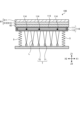
- FIG. 3 is a schematic diagram of the detection device according to the first embodiment.
- the detection device 100 includes a light source device 7, a container 110, an optical filter 82, an optical sensor 81, and a spring 5.
- the light source device 7 includes a light source substrate 72 and a plurality of point light sources (light-emitting elements) 71.
- the point light sources 71 are, for example, light-emitting diodes (LEDs). In this way, the light source device 7 includes a plurality of point light sources 71 arranged in a planar shape.
- the container 110 includes a mounting substrate 111 and a cover member 112.
- the container 110 is, for example, a petri dish.
- the container 110 is translucent.
- the mounting substrate 111 is disposed on the Z1 side relative to the light source device 7, and is a translucent substrate on which the object to be detected 114 is mounted.
- the container is arranged upside down compared to a normal container. That is, in a normal container, the mounting substrate is arranged on the lower side and the cover member is arranged on the upper side.
- the mounting substrate 111 is arranged on the upper side and the cover member 112 is arranged on the lower side, and the optical sensor 81 and the optical filter 82 are provided on the upper side (Z1 side) of the upside-down container 110, and the light source device 7 is provided on the lower side (Z2 side).
- a culture medium 113 is provided on the lower side of the mounting substrate 111, and a detectable substance 114 is applied on the culture medium 113 (the lower surface of the culture medium 113).
- the detectable substance 114 is, for example, a microorganism such as bacteria, or a sample containing a microorganism, which forms a colony on the culture medium 113 over time.
- the detectable substance 114 is not limited to bacteria, and may be other minute objects such as cells.
- the optical sensor 81 has an array substrate 811 and sensor pixels 812 (photodiodes 813, light detection elements).
- the optical sensor 81 is arranged overlapping the optical filter 82 on the Z1 side.
- a plurality of sensor pixels 812 are provided on the Z2 side surface of the array substrate 811.
- the optical filter 82 is an optical element that transmits the component of the light L irradiated from the point light source 71 that travels in a direction perpendicular to the optical sensor 81 toward the photodiode 813.
- the optical filter 82 is also called a collimating aperture or a collimator.
- Light L emitted from the point light source 71 passes through the cover member 112, culture medium 113, mounting substrate 111, and optical filter 82, and is irradiated toward the optical sensor 81.
- the amount of light irradiated to the photodiode 813 (light detection element) of the optical sensor 81 differs between the area overlapping with the detectable object 114 and the area not overlapping with the detectable object 114. This allows the optical sensor 81 to image the detectable object 114.
- the detection device 100 is a device that places the detectable object 114 contained in the container 110 between the light source device 7 and the optical sensor 81, and monitors changes in the detectable object 114 by imaging the detectable object 114 with the optical sensor 81.
- the array substrate 811 is formed using the substrate 21 as a base.
- Each of the sensor pixels 812 is configured with a photodiode 813, multiple transistors, and various wiring.
- the array substrate 811 has a detection area AA and a peripheral area GA.
- the detection area AA is an area in which a plurality of sensor pixels 812 (a plurality of photodiodes 813) are provided.
- the peripheral area GA is an area between the outer periphery of the detection area AA and the outer edge of the array substrate 811, and is an area in which a plurality of sensor pixels 812 are not provided.
- the gate line driving circuits 814A, 814B, the signal line driving circuit 815A, and the detection control circuit 816 are provided in the peripheral area GA.
- Each of the multiple sensor pixels 812 is an optical sensor having a photodiode 813 as a sensor element.
- Each photodiode 813 outputs an electrical signal according to the light irradiated thereon.
- the detection control circuit 816 is a circuit that supplies control signals Sa, Sb, and Sc to the gate line driving circuits 814A, 814B and the signal line driving circuit 815A, respectively, and controls their operation.
- the detection control circuit 816 includes a signal processing circuit that processes the detection signals Vdet from the multiple photodiodes 813.
- the detection control circuit 816 processes the detection signal Vdet from the multiple photodiodes 813 and outputs a sensor value So based on the detection signal Vdet to the host IC 75. In this way, the detection device 100 detects information related to the object to be detected 114.
- the light source device 7 has a light source substrate 72, a plurality of point light sources 71 formed on the light source substrate 72, gate line driving circuits 814C and 814D, a signal line driving circuit 815B, and a light emitting element control circuit 74.
- the multiple point light sources 71 are arranged in a matrix in an area that overlaps with the detection area AA of the light source board 72.
- the light source board 72 is a drive circuit board that drives each of the multiple light-emitting elements 85 by switching them between on (illuminated state) and off (non-illuminated state).
- the host IC 75 has a sensor value storage circuit 751, a sensor value calculation circuit 752, a light amount setting circuit 753, and a target value storage circuit 759 as control circuits on the optical sensor 81 side.
- the sensor value storage circuit 751 stores the sensor value So output from the detection control circuit 816 of the optical sensor 81.
- the sensor value calculation circuit 752 performs a predetermined calculation process on the sensor value So of the photodiode 813.
- the light intensity setting circuit 753 compares the sensor value So detected by the multiple photodiodes 813 with a preset target sensor value So-t obtained from the target value memory circuit 759 to set the light intensity for detection of the multiple point light sources 71.
- the target value memory circuit 759 stores the preset target sensor value So-t.
- the host IC 75 has a lighting pattern generation circuit 754 and a lighting pattern storage circuit 755 as control circuits on the light source device 7 side.
- the lighting pattern storage circuit 755 stores information on the light intensity of each of the multiple point light sources 71 in the light intensity setting mode.
- the host IC 75 further includes an image generation circuit 756.
- the image generation circuit 756 In the detection mode, the image generation circuit 756 generates an image of the object to be detected 114 based on the sensor values So output from the multiple photodiodes 813.
- FIG. 5 is a schematic diagram showing the projection area of the light emitted from a point light source.
- FIG. 6 is a schematic diagram of the detection device according to the first embodiment.
- FIG. 5 shows the projection area of the light without the optical filter 82 according to this embodiment.
- FIG. 7 is a schematic diagram of the light source device according to the first embodiment as viewed in a plane.
- FIG. 8 is a schematic diagram of the optical filter according to the first embodiment as viewed in a plane.
- a total of 16 point light sources 71 are provided.
- the 16 point light sources 71 are arranged at equal intervals in the X and Y directions.
- the distance between adjacent point light sources 71 in the X direction is distance d
- the distance between adjacent point light sources 71 in the Y direction is also distance d.
- the light emitted from one point light source 71 spreads radially as it moves upward (toward the Z1 side), so as shown in FIG. 5, the projection area IA of the light projected onto the optical sensor 81 without the optical filter 82 is a circle of radius r centered on the point light source 71.
- Adjacent projection areas IA in the X direction or Y direction have an overlapping portion P, shown by hatching. This overlapping portion P causes the image of the detected object 114 to become blurred or hazy.
- FIG. 7 a total of 16 point light sources 71 according to this embodiment are provided.
- the 16 point light sources 71 are arranged at equal intervals in the X and Y directions. Specifically, four rows are arranged along the X direction, and four columns are arranged along the Y direction.
- point light source 71-4, point light source 71-3, point light source 71-4, and point light source 71-3 are arranged from the X2 side to the X1 side.
- point light source 71-1, point light source 71-2, point light source 71-1, and point light source 71-2 are arranged from the X2 side to the X1 side.
- point light source 71-3, point light source 71-4, point light source 71-3, and point light source 71-4 are arranged from the X2 side to the X1 side.
- point light source 71-2, point light source 71-1, point light source 71-2, and point light source 71-1 are arranged from the X2 side to the X1 side.
- point light source 71-4, point light source 71-1, point light source 71-3, and point light source 71-2 are arranged from the Y2 side to the Y1 side.
- the optical filter 82 is divided into a total of 16 parts in plan view. That is, the optical filter 82 has 16 divided regions divided in the X direction (second direction) and the Y direction (second direction).
- the divided regions (divided regions 82-1 to 82-4) have a square shape in plan view and are arranged at equal intervals in the X direction and the Y direction.
- the 16 divided regions are arranged at equal intervals in a lattice pattern in the X direction and the Y direction. Specifically, four rows are arranged along the X direction, and four columns are arranged along the Y direction.
- divided regions 82-4, 82-3, 82-4, and 82-3 are arranged from the X2 side to the X1 side.
- divided regions 82-1, 82-2, 82-1, and 82-2 are arranged from the X2 side to the X1 side.
- divided areas 82-3, 82-4, 82-3, and 82-4 are arranged from the X2 side to the X1 side.
- divided areas 82-2, 82-1, 82-2, and 82-1 are arranged from the X2 side to the X1 side.
- each of the multiple divided regions overlaps with each of the multiple point light sources 71 when viewed from the Z direction.
- the second row of the multiple point light sources 71 includes point light source 71-1 (first point light source), point light source 71-2 (second point light source), point light source 71-1, and point light source 71-2 arranged from the X2 side to the X1 side
- the second row of the multiple divided regions of the optical filter 82 includes divided region 82-1 (first divided region), divided region 82-2 (second divided region), divided region 82-1, and divided region 82-2 arranged from the X2 side to the X1 side.
- the point light source 71-1 overlaps with the divided region 82-1 (first divided region), and the point light source 71-2 (second point light source) overlaps with the divided region 82-2 (second divided region).
- point light source 71-1 first point light source
- divided region 82-1 first divided region
- divided region 82-2 second divided region
- point light source 71-1 overlaps with divided region 82-1
- point light source 71-2 overlaps with divided region 82-2
- point light source 71-3 overlaps with divided region 82-3
- point light source 71-4 overlaps with divided region 82-4.
- Light L1 emitted from point light source 71-1 is irradiated onto the entire divided region 82-1 and part of divided region 82-2.
- light L2 emitted from point light source 71-2 is irradiated onto the entire divided region 82-2, part of divided region 82-1, and part of divided region 82-3
- Light L3 emitted from point light source 71-3 is irradiated onto the entire divided region 82-3, part of divided region 82-2, and part of divided region 82-4.
- Light L4 emitted from point light source 71-4 is irradiated onto the entire divided region 82-4, part of divided region 82-3, and part of divided region 82-1.
- the irradiation angle of the light emitted from point light source 71 is angle ⁇ 1
- 114A is the captured image of the object to be detected.
- Figure 9 is a schematic diagram showing the wavelength bands of the emitted light and transmitted light.
- the solid lines show the emitted light 210 from point light source 71-1 (first point light source) and the transmitted light 230 that has passed through division region 82-1 (first division region).
- the dashed lines show the emitted light 220 from point light source 71-2 (second point light source) and the transmitted light 240 that has passed through division region 82-2 (second division region).
- the emitted light 210 has a first emitted light wavelength band Lb1
- the transmitted light 230 has a first transmitted light wavelength band La1.
- the first emitted light wavelength band Lb1 overlaps with the first transmitted light wavelength band La1.
- the emitted light 220 has a second emitted light wavelength band Lb2, and the transmitted light 240 has a second transmitted light wavelength band La2.
- the second emitted light wavelength band Lb2 overlaps with the second transmitted light wavelength band La2.
- the first emitted light wavelength band Lb1 does not overlap with the second emitted light wavelength band Lb2.
- the first transmitted light wavelength band La1 does not overlap with the second transmitted light wavelength band La2.
- the emitted light from the multiple point light sources 71 may have four or more different wavelength bands, and the transmitted light passing through the multiple divided regions of the optical filter 82 may have four or more different wavelength bands.
- the detection device 100 includes a light source device 7 including a plurality of point light sources 71, a translucent mounting substrate 111 on which a detected object 114 is mounted, an optical filter 82 having a plurality of divided regions, and an optical sensor 81 including a plurality of photodiodes (photodetection elements) 813.
- the first point light source 71-1 overlaps with the first divided region 82-1 of the optical filter 82 when viewed from the Z direction.
- the first emitted light wavelength band Lb1 of the emitted light 210 emitted from the first point light source 71-1 overlaps with the first transmitted light wavelength band La1 of the transmitted light 230 that passes through the first divided region 82-1.
- the first division region 82-1 of the optical filter 82 and the first point light source 71-1 are arranged to overlap in the Z direction, and the first emitted light wavelength band Lb1 and the first transmitted light wavelength band La1 are overlapped. Therefore, the light passing through the first division region 82-1 of the optical filter 82 is limited to the emitted light 210 emitted from the first point light source 71-1, preventing light of multiple wavelength bands from entering a specific region of the optical sensor 81. This makes it possible to reduce blurring of the image captured by the optical sensor 81.
- the second point light source 71-2 is adjacent to the first point light source 71-1 in the second direction, and the second division region 82-2 of the optical filter 82 is adjacent to the first division region 82-1 in the second direction.
- the second point light source 71-2 overlaps with the second division region 82-2 when viewed from the Z direction.
- the second emitted light wavelength band Lb2 of the emitted light 220 emitted from the second point light source 71-2 overlaps with the second transmitted light wavelength band La2 of the transmitted light 240 that passes through the second division region 82-2, the first emitted light wavelength band Lb1 does not overlap with the second emitted light wavelength band Lb2, and the first transmitted light wavelength band La1 does not overlap with the second transmitted light wavelength band La2.
- this embodiment further suppresses light of multiple wavelength bands from being incident on a specific region of the optical sensor 81. This makes it possible to further reduce blurring of the image captured by the optical sensor 81.
- the multiple divided regions When viewed from the Z direction, the multiple divided regions are arranged in a grid pattern. This reduces the number of boundaries between adjacent divided regions and reduces blurring of the image captured by the optical sensor 81.
- the detection device 100A according to the second embodiment differs from the detection device 100 according to the first embodiment in that it includes a side wall 6.
- the side wall 6 will be described in detail below.
- the sidewall 6 separates the multiple point light sources 71 from each other.
- the sidewall 6 is a partition that separates the point light sources adjacent in the X direction and the point light sources adjacent in the Y direction.
- the sidewall 6 has a lattice shape.
- the sidewall 6 protrudes toward the Z1 side.
- the height of the sidewall 6 is higher than that of the point light sources 71.
- the sidewall 6 has visible light absorption properties that absorb at least a portion of visible light.
- the irradiation angle of the light emitted from the point light source 71 is angle ⁇ 2.
- the angle ⁇ 2 is smaller than the angle ⁇ 1 (see Figure 6).
- the irradiation angle of the light emitted from the point light source 71 is angle ⁇ 2, which is smaller than angle ⁇ 1 (see FIG. 6). That is, the side wall 6 restricts a portion of the light emitted from the point light source 71 toward the Z1 side, reducing the irradiation angle of the light. In addition, because the side wall 6 has visible light absorption properties, the amount of light reflected is smaller than that of a normal louver. As a result, the light irradiated to the divided area of the optical filter 82 can be more concentrated.
- Light source device 71 Point light source 71-1 Point light source (first point light source) 71-2 Point light source (second point light source) 71-3 Point light source 71-4 Point light source 72
- Light source substrate 81 Optical sensor 82
- Optical filter 82-1 Division area (first division area) 82-2 Divided area (second divided area) 82-3 Divided region 82-4 Divided region 100, 100A Detection device 110
- Container 111 Mounting substrate 114 Object to be detected 210, 220 Emitted light 230, 240 Transmitted light 811
- Array substrate 812 Sensor pixel 813 Photodiode (light detection element) L light La1 first transmitted light wavelength band La2 second transmitted light wavelength band Lb1 first emitted light wavelength band Lb2 second emitted light wavelength band
Landscapes
- Life Sciences & Earth Sciences (AREA)
- Health & Medical Sciences (AREA)
- Chemical & Material Sciences (AREA)
- Engineering & Computer Science (AREA)
- Organic Chemistry (AREA)
- Zoology (AREA)
- Bioinformatics & Cheminformatics (AREA)
- Physics & Mathematics (AREA)
- General Health & Medical Sciences (AREA)
- Biochemistry (AREA)
- Wood Science & Technology (AREA)
- Biomedical Technology (AREA)
- Biotechnology (AREA)
- Immunology (AREA)
- Analytical Chemistry (AREA)
- Biophysics (AREA)
- General Engineering & Computer Science (AREA)
- Pathology (AREA)
- Genetics & Genomics (AREA)
- Microbiology (AREA)
- General Physics & Mathematics (AREA)
- Proteomics, Peptides & Aminoacids (AREA)
- Medicinal Chemistry (AREA)
- Molecular Biology (AREA)
- Hematology (AREA)
- Urology & Nephrology (AREA)
- Food Science & Technology (AREA)
- Sustainable Development (AREA)
- Toxicology (AREA)
- Geophysics And Detection Of Objects (AREA)
Priority Applications (1)
| Application Number | Priority Date | Filing Date | Title |
|---|---|---|---|
| JP2025527589A JPWO2024262213A1 (https=) | 2023-06-20 | 2024-05-17 |
Applications Claiming Priority (2)
| Application Number | Priority Date | Filing Date | Title |
|---|---|---|---|
| JP2023-101112 | 2023-06-20 | ||
| JP2023101112 | 2023-06-20 |
Related Child Applications (1)
| Application Number | Title | Priority Date | Filing Date |
|---|---|---|---|
| US19/424,954 Continuation US20260126321A1 (en) | 2023-06-20 | 2025-12-18 | Detection device |
Publications (1)
| Publication Number | Publication Date |
|---|---|
| WO2024262213A1 true WO2024262213A1 (ja) | 2024-12-26 |
Family
ID=93935667
Family Applications (1)
| Application Number | Title | Priority Date | Filing Date |
|---|---|---|---|
| PCT/JP2024/018365 Ceased WO2024262213A1 (ja) | 2023-06-20 | 2024-05-17 | 検出装置 |
Country Status (2)
| Country | Link |
|---|---|
| JP (1) | JPWO2024262213A1 (https=) |
| WO (1) | WO2024262213A1 (https=) |
Citations (4)
| Publication number | Priority date | Publication date | Assignee | Title |
|---|---|---|---|---|
| JP2013033008A (ja) * | 2011-08-03 | 2013-02-14 | Sony Corp | 光学分析装置及び光学分析方法 |
| JP2017021020A (ja) * | 2015-07-10 | 2017-01-26 | ヤマト科学株式会社 | 組織試料分析装置及び組織試料分析システム |
| WO2020184485A1 (ja) * | 2019-03-14 | 2020-09-17 | 株式会社 東芝 | モニタリング装置、及びモニタリングシステム |
| WO2021100367A1 (ja) * | 2019-11-19 | 2021-05-27 | 富士フイルム株式会社 | 検査装置 |
-
2024
- 2024-05-17 JP JP2025527589A patent/JPWO2024262213A1/ja active Pending
- 2024-05-17 WO PCT/JP2024/018365 patent/WO2024262213A1/ja not_active Ceased
Patent Citations (4)
| Publication number | Priority date | Publication date | Assignee | Title |
|---|---|---|---|---|
| JP2013033008A (ja) * | 2011-08-03 | 2013-02-14 | Sony Corp | 光学分析装置及び光学分析方法 |
| JP2017021020A (ja) * | 2015-07-10 | 2017-01-26 | ヤマト科学株式会社 | 組織試料分析装置及び組織試料分析システム |
| WO2020184485A1 (ja) * | 2019-03-14 | 2020-09-17 | 株式会社 東芝 | モニタリング装置、及びモニタリングシステム |
| WO2021100367A1 (ja) * | 2019-11-19 | 2021-05-27 | 富士フイルム株式会社 | 検査装置 |
Also Published As
| Publication number | Publication date |
|---|---|
| JPWO2024262213A1 (https=) | 2024-12-26 |
Similar Documents
| Publication | Publication Date | Title |
|---|---|---|
| JP7303114B2 (ja) | バックライト光源、バックライトモジュールおよび表示装置 | |
| US8947747B2 (en) | Erecting equal-magnification lens array plate and image reading device | |
| US20170017145A1 (en) | High contrast projection screen with stray light rejection | |
| KR101931402B1 (ko) | 마이크로 렌즈 어레이 및 그것을 사용한 스캔 노광 장치 | |
| JP2021518031A5 (https=) | ||
| JP2017524985A (ja) | ピクセル数の多い表示装置用の有色無機ledディスプレイ | |
| KR20140024630A (ko) | 표시 장치 | |
| JP7114017B1 (ja) | 光固化3dプリンタの光学機器、プリンタ及び3d印刷方法 | |
| US9772550B2 (en) | Apparatus, system and method for mitigating contrast artifacts at an overlap region of a projected image | |
| CN1723688A (zh) | 导光单元以及具备其的图像读取装置 | |
| WO2024262213A1 (ja) | 検出装置 | |
| JP5825470B2 (ja) | 露光装置及び遮光板 | |
| US20260126321A1 (en) | Detection device | |
| US7989829B2 (en) | Light emitting diode backlight module and liquid crystal display | |
| KR20160125604A (ko) | 백라이트 유닛 및 이를 포함하는 표시 장치 | |
| CN220913346U (zh) | 用于激光雷达的光发射装置及激光雷达 | |
| KR20080048782A (ko) | 백라이트 유닛 및 이를 포함하는 디스플레이장치 | |
| US20250264358A1 (en) | Detection device | |
| CN114083798A (zh) | 光源组件及打印机 | |
| WO2025009272A1 (ja) | 検出装置 | |
| US12578601B2 (en) | Backlight and display device | |
| US20250264359A1 (en) | Detection device | |
| US20250044216A1 (en) | Detection device | |
| US20250189719A1 (en) | Detection device | |
| JP5141080B2 (ja) | 光源装置、及び、それを用いた画像表示装置、モニタ装置、並びに照明装置 |
Legal Events
| Date | Code | Title | Description |
|---|---|---|---|
| 121 | Ep: the epo has been informed by wipo that ep was designated in this application |
Ref document number: 24825621 Country of ref document: EP Kind code of ref document: A1 |
|
| ENP | Entry into the national phase |
Ref document number: 2025527589 Country of ref document: JP Kind code of ref document: A |
|
| WWE | Wipo information: entry into national phase |
Ref document number: 2025527589 Country of ref document: JP |
|
| NENP | Non-entry into the national phase |
Ref country code: DE |