WO2024257470A1 - 回路モジュール - Google Patents
回路モジュール Download PDFInfo
- Publication number
- WO2024257470A1 WO2024257470A1 PCT/JP2024/014999 JP2024014999W WO2024257470A1 WO 2024257470 A1 WO2024257470 A1 WO 2024257470A1 JP 2024014999 W JP2024014999 W JP 2024014999W WO 2024257470 A1 WO2024257470 A1 WO 2024257470A1
- Authority
- WO
- WIPO (PCT)
- Prior art keywords
- electrode
- end surface
- insulating member
- circuit module
- electronic component
- Prior art date
- Legal status (The legal status is an assumption and is not a legal conclusion. Google has not performed a legal analysis and makes no representation as to the accuracy of the status listed.)
- Ceased
Links
Images



Classifications
-
- H—ELECTRICITY
- H05—ELECTRIC TECHNIQUES NOT OTHERWISE PROVIDED FOR
- H05K—PRINTED CIRCUITS; CASINGS OR CONSTRUCTIONAL DETAILS OF ELECTRIC APPARATUS; MANUFACTURE OF ASSEMBLAGES OF ELECTRICAL COMPONENTS
- H05K3/00—Apparatus or processes for manufacturing printed circuits
- H05K3/30—Assembling printed circuits with electric components, e.g. with resistors
- H05K3/32—Assembling printed circuits with electric components, e.g. with resistors electrically connecting electric components or wires to printed circuits
- H05K3/34—Assembling printed circuits with electric components, e.g. with resistors electrically connecting electric components or wires to printed circuits by soldering
- H05K3/341—Surface mounted components
- H05K3/3431—Leadless components
- H05K3/3442—Leadless components having edge contacts, e.g. leadless chip capacitors, chip carriers
-
- H—ELECTRICITY
- H05—ELECTRIC TECHNIQUES NOT OTHERWISE PROVIDED FOR
- H05K—PRINTED CIRCUITS; CASINGS OR CONSTRUCTIONAL DETAILS OF ELECTRIC APPARATUS; MANUFACTURE OF ASSEMBLAGES OF ELECTRICAL COMPONENTS
- H05K1/00—Printed circuits
- H05K1/02—Details
- H05K1/0296—Conductive pattern lay-out details not covered by sub groups H05K1/02 - H05K1/0295
-
- H—ELECTRICITY
- H05—ELECTRIC TECHNIQUES NOT OTHERWISE PROVIDED FOR
- H05K—PRINTED CIRCUITS; CASINGS OR CONSTRUCTIONAL DETAILS OF ELECTRIC APPARATUS; MANUFACTURE OF ASSEMBLAGES OF ELECTRICAL COMPONENTS
- H05K1/00—Printed circuits
- H05K1/18—Printed circuits structurally associated with non-printed electric components
-
- H—ELECTRICITY
- H05—ELECTRIC TECHNIQUES NOT OTHERWISE PROVIDED FOR
- H05K—PRINTED CIRCUITS; CASINGS OR CONSTRUCTIONAL DETAILS OF ELECTRIC APPARATUS; MANUFACTURE OF ASSEMBLAGES OF ELECTRICAL COMPONENTS
- H05K1/00—Printed circuits
- H05K1/18—Printed circuits structurally associated with non-printed electric components
- H05K1/181—Printed circuits structurally associated with non-printed electric components associated with surface mounted components
-
- H—ELECTRICITY
- H05—ELECTRIC TECHNIQUES NOT OTHERWISE PROVIDED FOR
- H05K—PRINTED CIRCUITS; CASINGS OR CONSTRUCTIONAL DETAILS OF ELECTRIC APPARATUS; MANUFACTURE OF ASSEMBLAGES OF ELECTRICAL COMPONENTS
- H05K3/00—Apparatus or processes for manufacturing printed circuits
- H05K3/22—Secondary treatment of printed circuits
- H05K3/28—Applying non-metallic protective coatings
- H05K3/284—Applying non-metallic protective coatings for encapsulating mounted components
-
- H—ELECTRICITY
- H05—ELECTRIC TECHNIQUES NOT OTHERWISE PROVIDED FOR
- H05K—PRINTED CIRCUITS; CASINGS OR CONSTRUCTIONAL DETAILS OF ELECTRIC APPARATUS; MANUFACTURE OF ASSEMBLAGES OF ELECTRICAL COMPONENTS
- H05K3/00—Apparatus or processes for manufacturing printed circuits
- H05K3/30—Assembling printed circuits with electric components, e.g. with resistors
- H05K3/32—Assembling printed circuits with electric components, e.g. with resistors electrically connecting electric components or wires to printed circuits
- H05K3/34—Assembling printed circuits with electric components, e.g. with resistors electrically connecting electric components or wires to printed circuits by soldering
- H05K3/3405—Edge mounted components, e.g. terminals
-
- H—ELECTRICITY
- H05—ELECTRIC TECHNIQUES NOT OTHERWISE PROVIDED FOR
- H05K—PRINTED CIRCUITS; CASINGS OR CONSTRUCTIONAL DETAILS OF ELECTRIC APPARATUS; MANUFACTURE OF ASSEMBLAGES OF ELECTRICAL COMPONENTS
- H05K2201/00—Indexing scheme relating to printed circuits covered by H05K1/00
- H05K2201/10—Details of components or other objects attached to or integrated in a printed circuit board
- H05K2201/10007—Types of components
- H05K2201/1003—Non-printed inductor
-
- H—ELECTRICITY
- H05—ELECTRIC TECHNIQUES NOT OTHERWISE PROVIDED FOR
- H05K—PRINTED CIRCUITS; CASINGS OR CONSTRUCTIONAL DETAILS OF ELECTRIC APPARATUS; MANUFACTURE OF ASSEMBLAGES OF ELECTRICAL COMPONENTS
- H05K2201/00—Indexing scheme relating to printed circuits covered by H05K1/00
- H05K2201/10—Details of components or other objects attached to or integrated in a printed circuit board
- H05K2201/10613—Details of electrical connections of non-printed components, e.g. special leads
- H05K2201/10621—Components characterised by their electrical contacts
- H05K2201/10636—Leadless chip, e.g. chip capacitor or resistor
Definitions
- the present invention relates to a circuit module.
- a known example of a conventional circuit module invention is the circuit module described in Patent Document 1.
- the circuit module described in Patent Document 1 comprises a substrate module having an upper main surface, an electronic component disposed on the substrate module, and a bonding adhesive for fixing the electronic component to the upper main surface of the substrate module.
- the electronic component includes a first electrode.
- the substrate module includes a second electrode. The first electrode is electrically connected to the second electrode via solder.
- the manufacture of the circuit module described in Patent Document 1 may include a process (polishing process) of polishing the upper main surface of the substrate module to expose the second electrode from the upper main surface of the substrate module.
- a process polishing process
- the productivity of the circuit module described in Patent Document 1 deteriorates. Therefore, in the field of the circuit module described in Patent Document 1, there is a demand to reduce the polishing process during manufacture.
- the object of the present invention is to provide a circuit module that can eliminate the polishing process during manufacturing.
- a circuit module includes: a circuit board including a circuit board body having a first upper end surface and a first lower end surface aligned in a vertical direction, and a conductor provided on the first upper end surface; an insulating member disposed on the first upper end surface; a first electrode having a second upper end surface and a second lower end surface aligned in the vertical direction and a first side surface connected to the second upper end surface, the first electrode being electrically connected to the conductor; an electronic component including an electronic component body and a second electrode, the electronic component being disposed on the insulating member; Equipped with the second upper end surface is covered with the insulating member, The second electrode is electrically connected to the first electrode by at least a portion of the first side surface being exposed from the insulating member.
- the circuit module of the present invention can eliminate the polishing process during manufacturing.
- FIG. 1 is a perspective view of a circuit module 1.
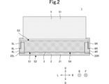
- FIG. FIG. 2 is a cross-sectional view of the circuit module 1 taken along line AA.
- FIG. 3 is a plan view of the insulating member 3 viewed from above.
- FIG. 4 is a perspective view of the insulating member 3 and the first electrodes 4L and 4R.
- FIG. 5 is a cross-sectional view of the insulating member 3 and the first electrodes 4L and 4R taken along the line BB.
- FIG. 6 is a perspective view of the electronic component 5.
- FIG. 7 is a cross-sectional view showing an example of a method for manufacturing the circuit module 1.
- FIG. 8 is a cross-sectional view of the circuit module 1a taken along line AA.
- FIG. 9 is a cross-sectional view of the circuit module 1b taken along line AA.
- FIG. 1 is a perspective view of the circuit module 1.
- Fig. 2 is a cross-sectional view of the circuit module 1 taken along line A-A.
- Fig. 3 is a plan view of the insulating member 3 viewed from above.
- Fig. 4 is a perspective view of the insulating member 3 and the first electrodes 4L and 4R.
- Fig. 5 is a cross-sectional view of the insulating member 3 and the first electrodes 4L and 4R taken along line B-B.
- Fig. 6 is a perspective view of an electronic component 5.
- directions are defined as follows. As shown in FIG. 1, the direction in which the bottom end surface S2 and the top end surface S1 of the circuit board main body 21 are arranged in this order is defined as the upward direction. The opposite direction of the upward direction is defined as the downward direction. As shown in FIG. 2, the direction in which the first electrodes 4L and the first electrodes 4R are arranged in this order is defined as the rightward direction. The opposite direction of the rightward direction is defined as the leftward direction. The rightward and leftward directions are perpendicular to the upward and downward directions. The direction perpendicular to the upward and rightward directions is defined as the forward direction. The opposite direction of the forward direction is defined as the rearward direction.
- the direction perpendicular to the up-down direction is defined as the horizontal direction.
- the rightward, leftward, forward, and rearward directions are examples of the horizontal direction.
- the upward, downward, rightward, leftward, forward, and rearward directions in this specification are directions defined for the convenience of explanation, and do not have to match the upward, downward, rightward, leftward, forward, and rearward directions when the circuit module 1 is in use.
- the top and bottom directions may be interchanged
- the right and left directions may be interchanged
- the front and rear directions may be interchanged.
- the positional relationship of the members is defined as follows.
- the first member to the third member constitute the circuit module 1.
- a first member being positioned above a second member includes cases where at least a portion of the first member is located directly above the second member, and cases where the first member is not located directly above the second member but is located diagonally above the second member. In this case, the first member does not have to overlap with the second member when viewed in the up-down direction. Diagonally above means, for example, top left or top right. This definition also applies to directions other than the upward direction.
- each part of the first member is defined as follows:
- the upper part of the first member means the upper half of the first member.
- the upper end of the first member means the upper end of the first member.
- the upper end part of the first member means the upper end of the first member and its vicinity. This definition also applies to directions other than the upward direction.
- the first member and the second member are electrically connected means that electricity is conducted between the first member and the second member. Therefore, the first member and the second member may be in direct contact with each other, or may not be in direct contact with each other. When the first member and the second member are not in direct contact with each other, a third member having electrical conductivity is disposed between the first member and the second member.
- the circuit module 1 includes a circuit board 2, an insulating member 3, a first electrode 4L, a first electrode 4R, an electronic component 5, solder 6L, and solder 6R.
- the circuit module 1 has a bilaterally symmetrical structure.
- the circuit board 2 includes a circuit board main body 21, a conductor 22L, and a conductor 22R.
- the conductor 22L has a structure that is symmetrical to the conductor 22R. Therefore, a description of the conductor 22L will be omitted.
- the circuit board 2 has upper and lower main surfaces that are aligned in the vertical direction. The upper main surface of the circuit board 2 is located above the lower main surface of the circuit board 2. As shown in FIG. 1, the circuit board 2 has a rectangular shape with long sides extending in the left-right direction and short sides extending in the front-rear direction when viewed in the vertical direction.
- the circuit board body 21 has an upper end surface S1 and a lower end surface S2 aligned in the vertical direction.
- the upper end surface S1 is located above the lower end surface S2.
- the upper end surface S1 is defined as the surface located at the upper end of the circuit board body 21. This definition also applies to end surfaces other than the upper end surface. This definition also applies to members other than the circuit board body 21.
- the circuit board body 21 has a left-right symmetrical structure. Therefore, the description of the left part of the circuit board body 21 is omitted.
- the upper end surface S1 is a part of the upper main surface of the circuit board 2.
- the lower end surface S2 is a part of the lower main surface of the circuit board 2.
- the circuit board body 21 When viewed in the vertical direction, the circuit board body 21 has a rectangular shape with long sides extending in the left-right direction and short sides extending in the front-rear direction.
- the right end surface of the circuit board body 21 is a part of the right surface of the circuit board 2.
- the front end surface of the circuit board body 21 is the same as the front surface of the circuit board 2.
- the rear end surface of the circuit board body 21 is the same as the rear surface of the circuit board 2.
- the upper end surface S1 corresponds to the "first upper end surface” of the present invention.
- the lower end surface S2 corresponds to the "first lower end surface" of the present invention.
- the conductor 22R is provided on the circuit board main body 21.
- the conductor 22R is provided on the right end of the circuit board main body 21.
- the conductor 22R is conductive.
- the conductor 22R has an upper surface and a lower surface aligned in the vertical direction.
- the upper surface of the conductor 22R is located above the lower surface of the conductor 22R.
- the upper surface of the conductor 22R is a part of the upper main surface of the circuit board 2.
- the lower surface of the conductor 22R is located above the lower main surface of the circuit board 2.
- the conductor 22R is electrically connected to the electric circuit inside the circuit board main body 21.
- the conductor 22R When viewed in the vertical direction, the conductor 22R has a rectangular shape with short sides extending in the left-right direction and long sides extending in the front-rear direction.
- the right surface of the conductor 22R is a part of the right surface of the circuit board 2.
- the material of the conductor 22R is, for example, a metal such as copper.
- the insulating member 3 has insulating properties.
- the insulating member 3 has a bilaterally symmetrical structure.
- the insulating member 3 has an upper end surface S3 and a lower end surface S4 aligned in the vertical direction.
- the upper end surface S3 is located above the lower end surface S4.
- the insulating member 3 is disposed on the upper end surface S1 of the circuit board body 21.
- the insulating member 3 covers the entire upper end surface S1 of the circuit board body 21.
- the insulating member 3 is, for example, a resin.
- Each of the upper end surface S3 and the lower end surface S4 has a rectangular shape with short sides extending in the left-right direction and long sides extending in the front-rear direction when viewed in the vertical direction.
- the lower end surface S4 has an area A1 that does not overlap with the upper end surface S3 when viewed in the vertical direction.
- the upper end surface S3 corresponds to the "third upper end surface” of the present invention.
- the lower end surface S4 corresponds to the "third lower end surface” of the present invention.
- each of the protrusions 31LB and 31LF has a structure that is symmetrical to each of the protrusions 31RB and 31RF. Therefore, a description of each of the protrusions 31LB and 31LF will be omitted.
- the protrusions 31RB and 31RF are lined up in this order toward the rear. The protrusions 31RB and 31RF are located in area A1 when viewed in the up-down direction.
- the lower end surface S4 has area A1.
- the protrusions 31RB and 31RF are parts of the insulating member 3 that are located in an area that does not overlap with the upper end surface S3.
- the upper surfaces of the protrusions 31RB and 31RF are not connected to the upper end surface S3.
- the upper surfaces of the protrusions 31RB and 31RF are located between the upper end surface S3 and the lower end surface S4 in the vertical direction.
- the lower surfaces of the protrusions 31RB and 31RF are parts of the lower end surface S4.
- the first electrode 4L and the first electrode 4R are conductive.
- the first electrode 4L has a structure that is symmetrical to the first electrode 4R. Therefore, a description of the first electrode 4L will be omitted.
- the first electrode 4R is disposed on the conductor 22R.
- the material of the first electrode 4R is, for example, a metal such as copper.
- the first electrode 4R is provided at the right end of the insulating member 3.
- the first electrode 4R has an upper end surface S5 and a lower end surface S6 aligned in the vertical direction, and a side surface SS1 connected to the upper end surface S5.
- the upper end surface S5 is located above the lower end surface S6.
- the first electrode 4R includes an electrode portion 4RE and a protrusion 4RP.
- the electrode portion 4RE has a rectangular shape extending in the vertical direction.
- the upper surface of the electrode portion 4RE is the upper end surface S5.
- the lower surface of the electrode portion 4RE is a part of the lower end surface S6.
- the upper surface of the electrode portion 4RE is not exposed because it is covered by the insulating member 3.
- the upper end surface S5 is not exposed because it is covered by the insulating member 3.
- the lower surface of the electrode portion 4RE is exposed from the insulating member 3.
- the lower end surface S6 is exposed from the insulating member 3.
- the electrode portion 4RE is fixed to the upper surface of the conductor 22R by solder (not shown). Therefore, the first electrode 4R is electrically connected to the conductor 22R.
- the right surface of the electrode portion 4RE is exposed from the insulating member 3.
- at least a portion of the side surface SS1 is exposed from the insulating member 3.
- the first electrode 4R is embedded in the right part of the insulating member 3 so that the right surface of the electrode portion 4RE is exposed.
- the upper end surface S5 corresponds to the "second upper end surface” of the present invention.
- the lower end surface S6 corresponds to the "second lower end surface” of the present invention.
- the side surface SS1 corresponds to the "first side surface” of the present invention.
- the protrusion 4RP is located to the right of the electrode portion 4RE. More specifically, the protrusion 4RP extends from the lower portion of the electrode portion 4RE to the right. As a result, the protrusion 4RP does not overlap with the upper end surface S5 of the first electrode 4R when viewed in the up-down direction.
- the protrusion 4RP is located below the upper end surface S5.
- the upper surface of the protrusion 4RP is exposed from the insulating member 3.
- the lower surface of the protrusion 4RP is exposed from the insulating member 3.
- the protrusion 4RP is fixed to the upper surface of the conductor 22R by solder (not shown).
- the right surface of the electrode portion 4RE is exposed from the insulating member 3.
- the protrusion 4RP is located between the protrusions 31RB and 31RF of the insulating member 3 in the front-rear direction. As a result, the front and rear surfaces of the protrusion 4RP are not exposed from the insulating member 3.
- the electronic component 5 includes an electronic component body 51, a second electrode 5L, and a second electrode 5R.
- the second electrode 5L and the second electrode 5R are conductive.
- the electronic component 5 is, for example, an inductor.
- the second electrode 5L has a structure symmetrical to the second electrode 5R. Therefore, the description of the second electrode 5L is omitted.
- the electronic component body 51 has a rectangular parallelepiped shape. Therefore, the electronic component body 51 has an upper main surface S7 and a lower main surface S8 aligned in the vertical direction, and a side surface SS2 connecting the upper main surface S7 and the lower main surface S8.
- the upper main surface S7 is located on the lower main surface S8.
- the electronic component 5 is disposed on the insulating member 3 as shown in FIG. 1.
- the electronic component body 51 overlaps the insulating member 3 when viewed in the vertical direction.
- the electronic component body 51 overlaps the first electrode 4L and the first electrode 4R when viewed in the vertical direction.
- the lower main surface S8 is not in contact with the upper end surface S3 of the insulating member 3.
- the side surface SS2 corresponds to the "second side surface" of the present invention.
- the second electrode 5R is provided on the right end of the electronic component body 51 as shown in FIG. 6. More specifically, the second electrode 5R has a shape extending from the right surface of the electronic component body 51 in a lower right direction. That is, the second electrode 5R has a shape extending from at least a part of the side surface SS2 of the electronic component body 51 in a lower right direction.
- the second electrode 5R has a first electrode portion 52R1 extending rightward from the right surface of the electronic component body 51, and a second electrode portion 52R2 extending downward from the right end of the first electrode portion 52R1. As a result, the lower end of the second electrode 5R is located below the lower main surface S8 of the electronic component body 51.
- the second electrode 5R overlaps with the protruding portion 4RP of the first electrode 4R when viewed in the up-down direction.
- the material of the second electrode 5R is, for example, a metal such as copper.
- the second electrode portion 52R2 corresponds to the "electrode portion" of the present invention.
- the electronic component 5 is fixed to the first electrode 4L and the first electrode 4R by the solder 6L and the solder 6R.
- the solder 6L has a structure symmetrical to the solder 6R. Therefore, the description of the solder 6L is omitted.
- the solder 6R is provided between the first electrode 4R and the second electrode 5R. More specifically, the solder 6R is located between the right surface of the electrode portion 4RE and the left surface of the second electrode portion 52R2, and is in contact with each of the right surface of the electrode portion 4RE and the left surface of the second electrode portion 52R2.
- the solder 6R fixes the left surface of the second electrode portion 52R2 to the right of the right surface of the electrode portion 4RE.
- the solder 6R is also located between the upper surface of the protrusion portion 4RP and the lower surface of the second electrode portion 52R2, and is in contact with each of the upper surface of the protrusion portion 4RP and the lower surface of the second electrode portion 52R2.
- the solder 6R fixes the lower surface of the second electrode portion 52R2 onto the upper surface of the protruding portion 4RP. That is, the second electrode 5R is electrically connected to the first electrode 4R because the right surface of the electrode portion 4RE of the first electrode 4R is exposed from the insulating member 3. Therefore, the second electrode 5R is electrically connected to the conductor 22R.
- a circuit board 2a having a plurality of conductors 22a provided on the upper end surface S1 of the circuit board main body 21, an insulating member 3a, and a plurality of electrodes 4a are prepared. Solder paste (not shown) is applied to the upper surface of each of the plurality of conductors 22a. At this time, the plurality of conductors 22a are arranged in the left-right direction. The plurality of electrodes 4a are arranged in the left-right direction. The insulating member 3a is also placed on the circuit board 2a. Each of the plurality of electrodes 4a is placed on each of the plurality of conductors 22a.
- the insulating member 3a and the multiple electrodes 4a are half-cut. More specifically, when viewed from the top-bottom direction, each of the multiple electrodes 4a and the insulating member 3a are cut so that in the areas overlapping each of the multiple electrodes 4a, an area including the entire outer edge of the upper surface of each of the multiple electrodes 4a and the lower end of each of the multiple electrodes 4a remain. This forms multiple recesses aR.
- solder paste 6a is filled into each of the multiple recesses aR.
- the vertical position of the upper end of each of the multiple solder pastes 6a is the same as the vertical position of the upper end of each of the multiple electrodes 4a. Note that the upper end of each of the multiple solder pastes 6a may be lower than the upper end of each of the multiple electrodes 4a.
- the multiple electronic components 5 are placed on the insulating member 3 so that the second electrodes 5L and the second electrodes 5R are inserted into the multiple solder pastes 6a, respectively.
- the circuit board 2a, the insulating member 3a, the multiple electrodes 4a, the multiple electronic components 5, and the solder pastes 6a are placed inside a reflow furnace and heated. This causes each of the multiple solder pastes 6a to melt.
- the circuit board 2a, the insulating member 3a, the multiple electrodes 4a, the multiple electronic components 5, and the solder pastes 6a are taken out of the reflow furnace and allowed to cool naturally. This causes each of the multiple molten solder pastes 6a to solidify. As a result, each of the multiple solder pastes 6a fixes the second electrodes 5L and the second electrodes 5R.
- the circuit board 2a, insulating member 3a, and multiple solder pastes 6a are fully cut. More specifically, in the left-right direction, the circuit board 2a, insulating member 3a, and multiple solder pastes 6a located in the area between the second electrode 5R of a certain electronic component 5 and the second electrode 5L of the electronic component 5 located immediately to the right of it are cut. This separates the circuit board 2a, insulating member 3a, and multiple solder pastes 6a. As a result, the circuit module 1 is completed.
- the polishing process during manufacturing can be eliminated. More specifically, the upper end surface S5 of the first electrode 4R is covered by the insulating member 3. Therefore, the upper end surface S5 of the first electrode 4R is not exposed from the insulating member 3. Meanwhile, at least a part of the side surface SS1 of the first electrode 4R is exposed from the insulating member 3.
- the polishing process of exposing the first electrode 4R from the insulating member 3 can be eliminated by polishing the insulating member 3.
- the heat dissipation of the first electrode can be easily improved. More specifically, at least a portion of the side surface SS1 of the first electrode 4R is exposed from the insulating member 3. Therefore, the area of the portion of the first electrode 4R exposed from the insulating member 3 can be easily made larger than the area of the portion of the first electrode exposed from the insulating member when the upper end surface of the first electrode is exposed from the insulating member. Furthermore, it is possible to suppress a decrease in the heat dissipation of the first electrode 4R due to the electronic component body 51. As a result, according to the circuit module 1, the heat dissipation of the first electrode can be easily improved.
- the circuit module 1 can be made smaller. More specifically, the electronic component body 51 overlaps with the first electrode 4L and the first electrode 4R when viewed in the vertical direction. Therefore, the left-right length of the circuit module 1 can be made shorter than the left-right length of a circuit module in which the electronic component body does not overlap with the first electrode when viewed in the vertical direction. As a result, the circuit module 1 can be made smaller.
- the circuit module 1 can prevent the electronic component 5 from shifting out of position. More specifically, when the upper end surface of the first electrode is exposed from the insulating member, solder paste is applied to the upper end surface of the first electrode, and the second electrode of the electronic component is mounted on the solder paste. After that, the solder paste melts due to heating, and the second electrode slides on the solder paste, which may cause the position of the second electrode to shift. On the other hand, according to the circuit module 1, at least a portion of the side surface SS1 of the first electrode 4R is exposed from the insulating member 3. In addition, the lower end of the second electrode 5R is located below the lower main surface S8 of the electronic component body 51.
- the second electrode 5R is electrically connected to the first electrode 4R.
- the solder paste 6a is located between the right surface of the electrode portion 4RE of the first electrode 4R and the left surface of the second electrode portion 52R2 of the second electrode 5R. Therefore, the risk of the second electrode 5R slipping on the solder paste 6a and shifting the position of the second electrode 5R can be reduced. As a result, the circuit module 1 can prevent the electronic component 5 from shifting its position.
- the circuit module 1 allows the electronic component 5 to be easily positioned. More specifically, the second electrode 5R overlaps with the protruding portion 4RP of the first electrode 4R when viewed in the vertical direction.
- the electronic component 5 can be positioned by arranging the electronic component 5 so that the second electrode 5R overlaps with the protruding portion 4RP of the first electrode 4R when viewed in the vertical direction. Therefore, the circuit module 1 allows the electronic component 5 to be easily positioned.
- the first electrode 4R includes a protrusion 4RP extending to the right, so that the solder 6R can be secured onto the protrusion 4RP of the first electrode 4R.
- FIG. 8 is a cross-sectional view of the circuit module 1a taken along line A-A. Note that, regarding the circuit module 1a according to the first modified example, only the parts that are different from the circuit module 1 according to the first embodiment will be described, and the rest will be omitted.
- Circuit module 1a differs from circuit module 1 in that it further includes adhesive member 7.
- the adhesive member 7 is provided between the electronic component 5 and the insulating member 3 in the front-rear direction. More specifically, the adhesive member 7 is provided between the upper end surface S3 of the insulating member 3 and the lower main surface S8 of the electronic component body 51. The adhesive member 7 fixes the electronic component 5 onto the insulating member 3.
- the adhesive member 7 may be conductive or insulating.
- the circuit module 1a as described above also has the same effect as the circuit module 1. Moreover, according to the circuit module 1a, the area on which the adhesive material is applied can be increased, and the adhesive material can be prevented from coming into contact with the solder. More specifically, the adhesive material 7 is provided between the upper end surface S3 of the insulating member 3 and the lower main surface S8 of the electronic component body 51. On the other hand, in the circuit module 1a, there is no solder between the upper end surface S3 of the insulating member 3 and the lower main surface S8 of the electronic component body 51. Therefore, the area on which the adhesive material 7 is applied can be increased. This allows the electronic component 5 to be fixed more firmly on the insulating member 3.
- the circuit module 1a can increase the area over which the adhesive material is applied and can prevent the adhesive material from coming into contact with the solder.
- Fig. 9 is a cross-sectional view of the circuit module 1b taken along line A-A. Note that, for the circuit module 1b according to the second modified example, only the differences from the circuit module 1 according to the first embodiment will be described, and the rest will be omitted.
- Circuit module 1b differs from circuit module 1 in that protrusions 31RB and 31RF are not provided at the right end of insulating member 3, protrusions 31LB and 31LF are not provided at the left end of insulating member 3, insulating member 3 has a slope S9 located between upper end surface S3 and lower end surface S4 in the up-down direction, first electrode 4L has second electrode portion 52L2 extending in second direction DIR2 from the left end of first electrode portion 52L1, and first electrode 4R has second electrode portion 52R2 extending in first direction DIR1 from the right end of first electrode portion 52R1.
- the insulating member 3 has a quadrangular pyramid shape with the upper end surface S3 as the upper base and the lower end surface S4 as the lower base. As shown in FIG. 9, the insulating member 3 also has a slope S9 located between the upper end surface S3 and the lower end surface S4 in the up-down direction. More specifically, when viewed in the front-to-back direction, the angle ⁇ 1 between the slope S9 and the lower end surface S4 is greater than 0 degrees and less than 90 degrees.
- the second electrode portion 52R2 extends in the first direction DIR1 from the right end of the first electrode portion 52R1.
- the first direction DIR1 is a direction that includes a downward component and is different from the downward direction.
- the first direction DIR1 is a downward and rightward direction.
- acute angles and obtuse angles there are two angles between the first direction DIR1 and the left-to-right direction: acute angles and obtuse angles. Of these, the acute angle is the angle ⁇ 2 between the first direction DIR1 and the left-to-right direction.
- the angle ⁇ 2 between the first direction DIR1 and the left-to-right direction is larger than the angle ⁇ 1 between the slope S9 and the bottom end surface S4 and smaller than 90 degrees.
- the solder 6R fixes the left surface of the second electrode portion 52R2 to the upper right of the slope S9.
- the circuit module 1b as described above also has the same effect as the circuit module 1. Moreover, according to the circuit module 1b, the first electrode 4R and the second electrode 5R can be easily electrically connected. More specifically, when viewed in the front-rear direction, the angle ⁇ 1 between the inclined surface S9 and the lower end surface S4 is greater than 0 degrees and less than 90 degrees. Also, when viewed in the front-rear direction, the angle ⁇ 2 between the first direction DIR1 in which the second electrode portion 52R2 extends and the left-right direction is greater than the angle ⁇ 1 between the inclined surface S9 and the lower end surface S4 and less than 90 degrees.
- the angle ⁇ 2 between the first direction DIR1 and the left-right direction is greater than the angle ⁇ 1 between the inclined surface S9 and the lower end surface S4, so that the second electrode portion 52R2 and the solder 6R are more likely to come into contact with each other, and the second electrode 5R and the first electrode 4R are more likely to be electrically connected.
- the angle ⁇ 2 between the first direction DIR1 and the left-right direction is less than 90 degrees, so that the contact area between the second electrode 5R and the solder 6R can be increased. This improves the reliability of the electrical connection between the first electrode 4R and the second electrode 5R.
- the circuit module 1b makes it easy to electrically connect the first electrode 4R and the second electrode 5R.
- the circuit module according to the present invention is not limited to the circuit module 1, the circuit module 1a, and the circuit module 1b, and may be modified within the scope of the present invention.
- the structures of the circuit module 1, the circuit module 1a, and the circuit module 1b may be combined in any manner.
- circuit module 1, circuit module 1a, and circuit module 1b do not have to have a bilaterally symmetrical structure.
- conductor 22L does not have to have a structure symmetrical to conductor 22R.
- the circuit board body 21 does not have to have a bilaterally symmetrical structure.
- the insulating member 3 does not have to have a symmetrical structure.
- protrusions 31LB and 31LF do not have to have a structure symmetrical to protrusions 31RB and 31RF, respectively.
- the first electrode 4L does not have to have a structure symmetrical with the first electrode 4R.
- the second electrode 5L does not have to have a structure symmetrical with the second electrode 5R.
- solder 6L does not have to have a bilaterally symmetrical structure with solder 6R.
- solder 6L and solder 6R are not essential components.
- protrusion 31RB, protrusion 31RF, protrusion 31LB, and protrusion 31LF are not essential components. Also, protrusion 4RP is not an essential component.
- the lower surfaces of the protrusions 31RB and 31RF may be located between the upper end surface S3 and the lower end surface S4 of the insulating member 3 in the vertical direction.
- the lower end surface S4 does not have to have the area A1 that does not overlap with the upper end surface S3 when viewed in the vertical direction.
- the electronic component body 51 does not have to overlap the first electrode 4L and the first electrode 4R when viewed in the vertical direction.
- the present invention has the following configuration.
- a circuit board including a circuit board body having a first upper end surface and a first lower end surface aligned in a vertical direction, and a conductor provided on the circuit board body; an insulating member disposed on the first upper end surface; a first electrode having a second upper end surface and a second lower end surface aligned in the vertical direction and a first side surface connected to the second upper end surface, the first electrode being electrically connected to the conductor; an electronic component including an electronic component body and a second electrode, the electronic component being disposed on the insulating member; Equipped with the second upper end surface is covered with the insulating member, the second electrode is electrically connected to the first electrode by at least a portion of the first side surface being exposed from the insulating member; Circuit module.
- the electronic component body has an upper main surface and a lower main surface aligned in the up-down direction, and a second side surface connecting the upper main surface and the lower main surface, the second electrode extends from at least a portion of the second side; A lower end of the second electrode is located below the lower main surface.
- the insulating member has a third upper end surface and a third lower end surface aligned in the up-down direction
- the electronic component body has an upper main surface and a lower main surface aligned in the up-down direction
- the adhesive member is provided between the third upper end surface and the lower main surface.
- the first electrode includes a protrusion extending in a horizontal direction perpendicular to the vertical direction, The protruding portion is located below the second upper end surface, The second electrode overlaps with the protruding portion when viewed in the up-down direction.
- a circuit module according to any one of (1) to (4).
- the insulating member has a third upper end surface and a third lower end surface aligned in the vertical direction, and a slope located between the third upper end surface and the third lower end surface in the vertical direction
- the second electrode has an electrode portion extending in a first direction that is a direction including a downward component and is different from the downward direction
- an angle between the inclined surface and the third lower end surface is greater than 0 degrees and less than 90 degrees
- an acute angle between the first direction and a left-right direction perpendicular to the up-down direction and the front-rear direction is greater than an angle between the inclined surface and the third lower end surface and is smaller than 90 degrees.
- a circuit module according to any one of (1) to (5).
- the electronic component is an inductor.
- a circuit module according to any one of (1) to (6).
- the insulating member is made of resin.
- a circuit module according to any one of (1) to (7).
Landscapes
- Engineering & Computer Science (AREA)
- Microelectronics & Electronic Packaging (AREA)
- Manufacturing & Machinery (AREA)
- Structures For Mounting Electric Components On Printed Circuit Boards (AREA)
Abstract
回路モジュールは、上下方向に並ぶ第1上端面及び第1下端面を有する回路基板本体と、第1上端面に設けられる導電体と、を含む回路基板と、第1上端面に配置される絶縁性部材と、上下方向に並ぶ第2上端面及び第2下端面と、第2上端面に繋がっている第1側面と、を有する第1電極であって、導電体と電気的に接続される第1電極と、電子部品本体と、第2電極と、を含む電子部品であって、絶縁性部材の上に配置される電子部品と、を備えている。第2上端面は、絶縁性部材に覆われており、第2電極は、第1側面の少なくとも一部分が絶縁性部材から露出していることにより、第1電極と電気的に接続される。
Description
本発明は、回路モジュールに関する。
従来の回路モジュールに関する発明としては、例えば、特許文献1に記載の回路モジュールが知られている。特許文献1に記載の回路モジュールは、上主面を有する基板モジュールと、基板モジュールの上に配置される電子部品と、電子部品を基板モジュールの上主面に固定するボンディング用接着剤と、を備えている。電子部品は、第1電極を含んでいる。基板モジュールは、第2電極を含んでいる。第1電極は、半田を介して、第2電極と電気的に接続されている。
特許文献1に記載の回路モジュールの製造において、基板モジュールの上主面を研磨することにより、基板モジュールの上主面から第2電極を露出させる工程(研磨工程)を含むことがある。この場合、特許文献1に記載の回路モジュールの生産性が悪化する。そこで、特許文献1に記載の回路モジュールの分野において、製造時の研磨工程を削減したいという要望がある。
そこで、本発明の目的は、製造時の研磨工程を削減することができる回路モジュールを提供することである。
本発明の一形態に係る回路モジュールは、
上下方向に並ぶ第1上端面及び第1下端面を有する回路基板本体と、前記第1上端面に設けられる導電体と、を含む回路基板と、
前記第1上端面に配置される絶縁性部材と、
前記上下方向に並ぶ第2上端面及び第2下端面と、前記第2上端面に繋がっている第1側面と、を有する第1電極であって、前記導電体と電気的に接続される第1電極と、
電子部品本体と、第2電極と、を含む電子部品であって、前記絶縁性部材の上に配置される電子部品と、
を備えており、
前記第2上端面は、前記絶縁性部材に覆われており、
前記第2電極は、前記第1側面の少なくとも一部分が前記絶縁性部材から露出していることにより、前記第1電極と電気的に接続される。
上下方向に並ぶ第1上端面及び第1下端面を有する回路基板本体と、前記第1上端面に設けられる導電体と、を含む回路基板と、
前記第1上端面に配置される絶縁性部材と、
前記上下方向に並ぶ第2上端面及び第2下端面と、前記第2上端面に繋がっている第1側面と、を有する第1電極であって、前記導電体と電気的に接続される第1電極と、
電子部品本体と、第2電極と、を含む電子部品であって、前記絶縁性部材の上に配置される電子部品と、
を備えており、
前記第2上端面は、前記絶縁性部材に覆われており、
前記第2電極は、前記第1側面の少なくとも一部分が前記絶縁性部材から露出していることにより、前記第1電極と電気的に接続される。
本発明に係る回路モジュールによれば、製造時の研磨工程を削減することができる。
[第1の実施形態]
[回路モジュール1の構造]
以下に、本発明の第1の実施形態に係る回路モジュール1について、図面を参照しながら説明する。図1は、回路モジュール1の斜視図である。図2は、回路モジュール1のA-Aにおける断面図である。図3は、絶縁性部材3を上方向に視た平面図である。図4は、絶縁性部材3及び第1電極4L及び第1電極4Rの斜視図である。図5は、絶縁性部材3及び第1電極4L及び第1電極4RのB-Bにおける断面図である。図6は、電子部品5の斜視図である。
[回路モジュール1の構造]
以下に、本発明の第1の実施形態に係る回路モジュール1について、図面を参照しながら説明する。図1は、回路モジュール1の斜視図である。図2は、回路モジュール1のA-Aにおける断面図である。図3は、絶縁性部材3を上方向に視た平面図である。図4は、絶縁性部材3及び第1電極4L及び第1電極4Rの斜視図である。図5は、絶縁性部材3及び第1電極4L及び第1電極4RのB-Bにおける断面図である。図6は、電子部品5の斜視図である。
本明細書において、方向を以下のように定義する。図1に示すように、回路基板本体21の下端面S2及び上端面S1がこの順に並ぶ方向を上方向と定義する。また、上方向の反対方向を下方向と定義する。また、図2に示すように、第1電極4L及び第1電極4Rがこの順に並ぶ方向を右方向と定義する。右方向の反対方向を左方向と定義する。右方向及び左方向は、上方向及び下方向に直交する。また、上方向及び右方向に直交する方向を前方向と定義する。前方向の反対方向を後方向と定義する。また、上下方向に直交する方向を水平方向と定義する。右方向、左方向、前方向及び後方向は、水平方向の一例である。ただし、本明細書における上方向、下方向、右方向、左方向、前方向及び後方向は、説明の便宜上定義した方向であり、回路モジュール1の使用時における上方向、下方向、右方向、左方向、前方向及び後方向と一致していなくてもよい。また、各図面において、上方向と下方向とを入れ替えてもよいし、右方向と左方向とを入れ替えてもよいし、前方向と後方向とを入れ替えてもよい。
本明細書において、部材の位置関係を以下のように定義する。第1部材乃至第3部材は、回路モジュール1の構成である。本明細書において、第1部材が第2部材の上に配置されるとは、以下の状態を指す。第1部材の少なくとも一部は、第2部材の真上に位置している。従って、上下方向に視て、第1部材は、第2部材と重なっている。この定義は、上方向以外の方向にも適用される。
本明細書において、第1部材が第2部材より上に配置されるとは、第1部材の少なくとも一部が第2部材の真上に位置している場合、及び、第1部材が第2部材の真上に位置せずに第1部材が第2部材の斜め上に位置している場合を含む。この場合、上下方向に視て、第1部材は、第2部材と重なっていなくてもよい。斜め上とは、例えば、左上、右上である。この定義は、上方向以外の方向にも適用される。
本明細書において、特に断りのない場合には、第1部材の各部について以下のように定義する。第1部材の上部とは、第1部材の上半分を意味する。第1部材の上端とは、第1部材の上方向の端を意味する。第1部材の上端部とは、第1部材の上端及びその近傍を意味する。この定義は、上方向以外の方向にも適用される。
本明細書において、「第1部材と第2部材とが電気的に接続される」とは、第1部材と第2部材との間で電気が導通していることを意味する。従って、第1部材と第2部材とが直接接触していてもよいし、第1部材と第2部材とが直接接触していなくてもよい。第1部材と第2部材とが直接接触していない場合には、第1部材と第2部材との間に導電性を有する第3部材が配置されている。
回路モジュール1は、図1及び図2に示すように、回路基板2、絶縁性部材3、第1電極4L、第1電極4R、電子部品5、半田6L及び半田6Rを備えている。本実施形態では、回路モジュール1は、左右対称な構造を有している。
回路基板2は、図2に示すように、回路基板本体21、導電体22L及び導電体22Rを含んでいる。なお、本実施形態では、導電体22Lは、導電体22Rと左右対称な構造を有している。そのため、導電体22Lの説明を省略する。回路基板2は、上下方向に並ぶ上主面及び下主面を有している。回路基板2の上主面は、回路基板2の下主面の上に位置している。回路基板2は、図1に示すように、上下方向に視て、左右方向に延びる長辺及び前後方向に延びる短辺を有する矩形状を有している。
回路基板本体21は、上下方向に並ぶ上端面S1及び下端面S2を有している。上端面S1は、下端面S2の上に位置している。ここで、上端面S1を回路基板本体21の上端に位置する面と定義する。この定義は、上端面以外の端面にも適用される。また、この定義は、回路基板本体21以外の部材にも適用される。なお、本実施形態では、回路基板本体21は、左右対称な構造を有している。そのため、回路基板本体21の左部の説明を省略する。上端面S1は、回路基板2の上主面の一部分である。また、下端面S2は、回路基板2の下主面の一部分である。回路基板本体21の内部には、導体層により電気回路が形成されている。回路基板本体21は、上下方向に視て、左右方向に延びる長辺及び前後方向に延びる短辺を有する矩形状を有している。回路基板本体21の右端面は、回路基板2の右面の一部分である。回路基板本体21の前端面は、回路基板2の前面と同一である。回路基板本体21の後端面は、回路基板2の後面と同一である。なお、上端面S1は、本発明の「第1上端面」に対応する。下端面S2は、本発明の「第1下端面」に対応する。
導電体22Rは、回路基板本体21に設けられている。また、導電体22Rは、回路基板本体21の右端部に設けられている。導電体22Rは、導電性を有している。導電体22Rは、上下方向に並ぶ上面及び下面を有している。導電体22Rの上面は、導電体22Rの下面の上に位置している。導電体22Rの上面は、回路基板2の上主面の一部分である。導電体22Rの下面は、回路基板2の下主面の上に位置している。導電体22Rは、回路基板本体21の内部の電気回路と電気的に接続されている。導電体22Rは、上下方向に視て、左右方向に延びる短辺及び前後方向に延びる長辺を有する矩形状を有している。導電体22Rの右面は、回路基板2の右面の一部分である。導電体22Rの材料は、例えば、銅等の金属である。
絶縁性部材3は、絶縁性を有している。本実施形態では、絶縁性部材3は、左右対称な構造を有している。絶縁性部材3は、上下方向に並ぶ上端面S3及び下端面S4を有している。上端面S3は、下端面S4の上に位置している。絶縁性部材3は、回路基板本体21の上端面S1に配置されている。本実施形態では、絶縁性部材3は、回路基板本体21の上端面S1の全体を覆っている。絶縁性部材3は、例えば、樹脂である。上端面S3及び下端面S4のそれぞれは、上下方向に視て、左右方向に延びる短辺及び前後方向に延びる長辺を有する矩形状を有している。ただし、本実施形態では、図3に示すように、下端面S4は、上下方向に視て、上端面S3と重ならない領域A1を有している。なお、上端面S3は、本発明の「第3上端面」に対応する。下端面S4は、本発明の「第3下端面」に対応する。
図3及び図4に示すように、絶縁性部材3の右端部には、突出部31RB及び突出部31RFが設けられている。また、絶縁性部材3の左端部には、突出部31LB及び突出部31LFが設けられている。なお、本実施形態では、突出部31LB及び突出部31LFのそれぞれは、突出部31RB及び突出部31RFのそれぞれと左右対称な構造を有している。そのため、突出部31LB及び突出部31LFのそれぞれの説明を省略する。突出部31RB及び突出部31RFは、後方向にこの順に並んでいる。突出部31RB及び突出部31RFは、上下方向に視て、領域A1に位置している。言い換えると、絶縁性部材3の右端部に突出部31RB及び突出部31RFが設けられていることにより、下端面S4は、領域A1を有している。突出部31RB及び突出部31RFは、絶縁性部材3を下方向に視たときに、上端面S3と重ならない領域に位置する絶縁性部材3の一部分である。また、突出部31RB及び突出部31RFの上面は、上端面S3に繋がっていない。突出部31RB及び突出部31RFの上面は、上下方向において、上端面S3と下端面S4との間に位置している。一方、突出部31RB及び突出部31RFの下面は、下端面S4の一部分である。
第1電極4L及び第1電極4Rは、導電性を有している。なお、本実施形態では、第1電極4Lは、第1電極4Rと左右対称な構造を有している。そのため、第1電極4Lの説明を省略する。第1電極4Rは、導電体22Rの上に配置されている。第1電極4Rの材料は、例えば、銅等の金属である。
第1電極4Rは、絶縁性部材3の右端部に設けられている。第1電極4Rは、上下方向に並ぶ上端面S5及び下端面S6と、上端面S5に繋がっている側面SS1と、を有している。上端面S5は、下端面S6の上に位置している。第1電極4Rは、図4及び図5に示すように、電極部4RE及び突出部4RPを含んでいる。電極部4REは、上下方向に延びる矩形状を有している。電極部4REの上面は、上端面S5である。電極部4REの下面は、下端面S6の一部分である。電極部4REの上面は、絶縁性部材3に覆われていることにより、露出していない。すなわち、上端面S5は、絶縁性部材3に覆われていることにより、露出していない。一方、電極部4REの下面は、絶縁性部材3から露出している。すなわち、下端面S6は、絶縁性部材3から露出している。これにより、電極部4REは、半田(図示せず)により、導電体22Rの上面に固定される。従って、第1電極4Rは、導電体22Rと電気的に接続されている。また、電極部4REの右面は、絶縁性部材3から露出している。すなわち、側面SS1の少なくとも一部分は、絶縁性部材3から露出している。第1電極4Rは、電極部4REの右面が露出するように、絶縁性部材3の右部に埋め込まれている。なお、上端面S5は、本発明の「第2上端面」に対応する。下端面S6は、本発明の「第2下端面」に対応する。側面SS1は、本発明の「第1側面」に対応する。
突出部4RPは、電極部4REの右に位置している。より詳細には、突出部4RPは、電極部4REの下部から右方向に延びている。これにより、突出部4RPは、上下方向に視て、第1電極4Rの上端面S5と重ならない。また、突出部4RPは、上端面S5より下に位置している。また、突出部4RPの上面は、絶縁性部材3から露出している。また、突出部4RPの下面は、絶縁性部材3から露出している。これにより、突出部4RPは、半田(図示せず)により、導電体22Rの上面に固定される。また、電極部4REの右面は、絶縁性部材3から露出している。一方、突出部4RPは、前後方向において、絶縁性部材3の突出部31RBと31RFとの間に位置している。これにより、突出部4RPの前面及び後面のそれぞれは、絶縁性部材3から露出していない。
電子部品5は、図6に示すように、電子部品本体51、第2電極5L及び第2電極5Rを含んでいる。第2電極5L及び第2電極5Rは、導電性を有している。電子部品5は、例えば、インダクタである。なお、本実施形態では、第2電極5Lは、第2電極5Rと左右対称な構造を有している。そのため、第2電極5Lの説明を省略する。電子部品本体51は、図6に示すように、直方体形状を有している。従って、電子部品本体51は、上下方向に並ぶ上主面S7及び下主面S8と、上主面S7と下主面S8とを繋ぐ側面SS2と、を有している。上主面S7は、下主面S8の上に位置している。また、電子部品5は、図1に示すように、絶縁性部材3の上に配置されている。電子部品本体51は、上下方向に視て、絶縁性部材3と重なっている。また、電子部品本体51は、上下方向に視て、第1電極4L及び第1電極4Rと重なっている。下主面S8は、図2に示すように、絶縁性部材3の上端面S3と接触していない。側面SS2は、本発明の「第2側面」に対応する。
第2電極5Rは、図6に示すように、電子部品本体51の右端部に設けられている。より詳細には、第2電極5Rは、電子部品本体51の右面から右下方向に延びる形状を有している。すなわち、第2電極5Rは、電子部品本体51の側面SS2の少なくとも一部分から右下方向に延びる形状を有している。第2電極5Rは、電子部品本体51の右面から右方向に延びる第1電極部52R1、及び、第1電極部52R1の右端部から下方向に延びる第2電極部52R2を有している。これにより、第2電極5Rの下端は、電子部品本体51の下主面S8より下に位置している。また、第2電極5Rは、上下方向に視て、第1電極4Rの突出部4RPと重なっている。第2電極5Rの材料は、例えば、銅等の金属である。なお、第2電極部52R2は、本発明の「電極部」に対応する。
電子部品5は、図1及び図2に示すように、半田6L及び半田6Rにより、第1電極4L及び第1電極4Rに固定される。なお、本実施形態では、半田6Lは、半田6Rと左右対称な構造を有している。そのため、半田6Lの説明を省略する。半田6Rは、第1電極4Rと第2電極5Rとの間に設けられている。より詳細には、半田6Rは、電極部4REの右面と第2電極部52R2の左面との間に位置しており、かつ、電極部4REの右面及び第2電極部52R2の左面のそれぞれと接触している。これにより、半田6Rは、第2電極部52R2の左面を電極部4REの右面の右に固定している。また、突出部4RPの上面と第2電極部52R2の下面との間に位置しており、かつ、突出部4RPの上面及び第2電極部52R2の下面のそれぞれと接触している。これにより、半田6Rは、第2電極部52R2の下面を突出部4RPの上面の上に固定している。すなわち、第2電極5Rは、第1電極4Rの電極部4REの右面が絶縁性部材3から露出していることにより、第1電極4Rと電気的に接続されている。従って、第2電極5Rは、導電体22Rと電気的に接続されている。
[回路モジュール1の製造方法]
次に、回路モジュール1の製造方法の一例について、図面を参照しながら説明する。図7は、回路モジュール1の製造方法の一例を示す断面図である。
次に、回路モジュール1の製造方法の一例について、図面を参照しながら説明する。図7は、回路モジュール1の製造方法の一例を示す断面図である。
まず、複数の導電体22aが回路基板本体21の上端面S1に設けられている回路基板2a、絶縁性部材3a、及び、複数の電極4aを準備する。複数の導電体22aのそれぞれの上面には、半田ペースト(図示せず)が塗られている。このとき、複数の導電体22aは、左右方向に並べられる。複数の電極4aは、左右方向に並べられる。また、絶縁性部材3aは、回路基板2aの上に配置される。複数の電極4aのそれぞれは、複数の導電体22aのそれぞれの上に配置される。
次に、絶縁性部材3a及び複数の電極4aをハーフカットする。より詳細には、上下方向に視て、複数の電極4aのそれぞれと重なる領域において、複数の電極4aのそれぞれの上面の外縁の全体を含む領域、及び、複数の電極4aのそれぞれの下端部が残るように、複数の電極4aのそれぞれ及び絶縁性部材3aを切る。これにより、複数の凹部aRが形成される。
次に、複数の凹部aRのそれぞれに半田ペースト6aを充填する。複数の半田ペースト6aのそれぞれの上端の上下方向の位置は、複数の電極4aのそれぞれの上端の上下方向の位置と同じである。なお、複数の半田ペースト6aのそれぞれの上端は、複数の電極4aのそれぞれの上端より下でもよい。
次に、複数の電子部品5を、第2電極5L及び第2電極5Rが複数の半田ペースト6aのそれぞれ内に挿入されるように、絶縁性部材3の上に配置する。その後、回路基板2a、絶縁性部材3a、複数の電極4a、複数の電子部品5及び半田ペースト6aをリフロー炉の内部に入れ、加熱する。これにより、複数の半田ペースト6aのそれぞれが溶融する。その後、回路基板2a、絶縁性部材3a、複数の電極4a、複数の電子部品5及び半田ペースト6aをリフロー炉の外部に取り出し、自然冷却する。これにより、溶融した複数の半田ペースト6aのそれぞれが固化する。これに伴い、複数の半田ペースト6aのそれぞれは、第2電極5L及び第2電極5Rを固定する。
次に、回路基板2a、絶縁性部材3a及び複数の半田ペースト6aをフルカットする。より詳細には、左右方向において、ある電子部品5の第2電極5Rと、その右隣に位置する電子部品5の第2電極5Lとの間の領域に位置する回路基板2a、絶縁性部材3a及び複数の半田ペースト6aを切る。これにより、回路基板2a、絶縁性部材3a及び複数の半田ペースト6aのそれぞれが分断される。その結果、回路モジュール1が完成する。
[効果]
回路モジュール1によれば、製造時の研磨工程を削減することができる。より詳細には、第1電極4Rの上端面S5は、絶縁性部材3に覆われている。従って、第1電極4Rの上端面S5は、絶縁性部材3から露出していない。一方、第1電極4Rの側面SS1の少なくとも一部分が絶縁性部材3から露出している。回路モジュール1の製造時に、絶縁性部材3a及び電極4aをハーフカットすることにより、第1電極4Rの側面SS1の少なくとも一部分を絶縁性部材3から露出させることができる。これにより、第1電極4Rと第2電極5Rとを電気的に接続することができる。従って、回路モジュール1によれば、絶縁性部材3を研磨することにより、絶縁性部材3から第1電極4Rを露出させる研磨工程を削減することができる。
回路モジュール1によれば、製造時の研磨工程を削減することができる。より詳細には、第1電極4Rの上端面S5は、絶縁性部材3に覆われている。従って、第1電極4Rの上端面S5は、絶縁性部材3から露出していない。一方、第1電極4Rの側面SS1の少なくとも一部分が絶縁性部材3から露出している。回路モジュール1の製造時に、絶縁性部材3a及び電極4aをハーフカットすることにより、第1電極4Rの側面SS1の少なくとも一部分を絶縁性部材3から露出させることができる。これにより、第1電極4Rと第2電極5Rとを電気的に接続することができる。従って、回路モジュール1によれば、絶縁性部材3を研磨することにより、絶縁性部材3から第1電極4Rを露出させる研磨工程を削減することができる。
また、回路モジュール1によれば、第1電極の放熱性を容易に向上することができる。より詳細には、第1電極4Rの側面SS1の少なくとも一部分は、絶縁性部材3から露出している。従って、第1電極4Rが絶縁性部材3から露出する部分の面積を、第1電極の上端面が絶縁性部材から露出する場合の第1電極が絶縁性部材から露出する部分の面積より容易に大きくすることができる。また、電子部品本体51により第1電極4Rの放熱性が低下することを抑制することができる。その結果、回路モジュール1によれば、第1電極の放熱性を容易に向上することができる。
また、回路モジュール1によれば、回路モジュールを小型化することができる。より詳細には、電子部品本体51は、上下方向に視て、第1電極4L及び第1電極4Rと重なっている。従って、回路モジュール1の左右方向の長さを、電子部品本体が、上下方向に視て、第1電極と重なっていない回路モジュールの左右方向の長さより短くすることができる。その結果、回路モジュール1によれば、回路モジュールを小型化することができる。
また、回路モジュール1によれば、電子部品5の位置がずれることを抑制することができる。より詳細には、第1電極の上端面が絶縁性部材から露出する場合、第1電極の上端面に半田ペーストが塗られ、半田ペーストの上に電子部品の第2電極を搭載する。その後、加熱により、半田ペーストが溶融し、第2電極が半田ペースト上を滑ることにより、第2電極の位置がずれるおそれがある。一方、回路モジュール1によれば、第1電極4Rの側面SS1の少なくとも一部分が、絶縁性部材3から露出している。また、第2電極5Rの下端は、電子部品本体51の下主面S8より下に位置している。これらにより、第2電極5Rは、第1電極4Rと電気的に接続される。半田ペースト6aは、第1電極4Rの電極部4REの右面と第2電極5Rの第2電極部52R2の左面との間に位置している。従って、第2電極5Rが半田ペースト6a上を滑ることにより、第2電極5Rの位置がずれるおそれを抑制することができる。その結果、回路モジュール1によれば、電子部品5の位置がずれることを抑制することができる。
また、回路モジュール1によれば、電子部品5を容易に位置決めすることができる。より詳細には、第2電極5Rは、上下方向に視て、第1電極4Rの突出部4RPと重なっている。第2電極5Rが、上下方向に視て、第1電極4Rの突出部4RPと重なるように、電子部品5を配置することにより、電子部品5を位置決めすることができる。従って、回路モジュール1によれば、電子部品5を容易に位置決めすることができる。
また、回路モジュール1によれば、第1電極4Rが右方向に延びている突出部4RPを含んでいることにより、半田6Rを第1電極4Rの突出部4RP上に留めることができる。
[第1の変形例]
以下に、本発明の第1の変形例に係る回路モジュール1aの構造について、図面を参照しながら説明する。図8は、回路モジュール1aのA-Aにおける断面図である。なお、第1の変形例に係る回路モジュール1aについては、第1の実施形態に係る回路モジュール1と異なる部分のみ説明し、後は省略する。
以下に、本発明の第1の変形例に係る回路モジュール1aの構造について、図面を参照しながら説明する。図8は、回路モジュール1aのA-Aにおける断面図である。なお、第1の変形例に係る回路モジュール1aについては、第1の実施形態に係る回路モジュール1と異なる部分のみ説明し、後は省略する。
回路モジュール1aは、接着部材7を更に備えている点において、回路モジュール1と相違する。
接着部材7は、図8に示すように、前後方向において、電子部品5と絶縁性部材3との間に設けられている。より詳細には、接着部材7は、絶縁性部材3の上端面S3と電子部品本体51の下主面S8との間に設けられている。接着部材7は、電子部品5を絶縁性部材3の上に固定している。接着部材7は、導電性を有していてもよいし、絶縁性を有していてもよい。
以上のような回路モジュール1aにおいても、回路モジュール1と同じ効果を奏する。また、回路モジュール1aによれば、接着部材を塗る面積を大きくすることができ、かつ、接着部材が半田と接触することを抑制することができる。より詳細には、接着部材7は、絶縁性部材3の上端面S3と電子部品本体51の下主面S8との間に設けられている。一方、回路モジュール1aにおいて、絶縁性部材3の上端面S3と電子部品本体51の下主面S8との間には、半田が存在しない。従って、接着部材7を塗る面積を大きくすることができる。これにより、電子部品5を絶縁性部材3の上により強固に固定することができる。また、接着部材7を塗る面積を大きくしたとしても、絶縁性部材3の上端面S3と電子部品本体51の下主面S8との間には、半田が存在しないため、接着部材7は、半田6L及び半田6Rと接触しにくい。従って、接着部材7が半田6L及び半田6Rと接触することを抑制することができる。その結果、回路モジュール1aによれば、接着部材を塗る面積を大きくすることができ、かつ、接着部材が半田と接触することを抑制することができる。
[第2の変形例]
以下に、本発明の第2の変形例に係る回路モジュール1bの構造について、図面を参照しながら説明する。図9は、回路モジュール1bのA-Aにおける断面図である。なお、第2の変形例に係る回路モジュール1bについては、第1の実施形態に係る回路モジュール1と異なる部分のみ説明し、後は省略する。
以下に、本発明の第2の変形例に係る回路モジュール1bの構造について、図面を参照しながら説明する。図9は、回路モジュール1bのA-Aにおける断面図である。なお、第2の変形例に係る回路モジュール1bについては、第1の実施形態に係る回路モジュール1と異なる部分のみ説明し、後は省略する。
回路モジュール1bは、絶縁性部材3の右端部に突出部31RB及び突出部31RFが設けられていない点、絶縁性部材3の左端部に突出部31LB及び突出部31LFが設けられていない点、絶縁性部材3が、上下方向において、上端面S3と下端面S4との間に位置している斜面S9を有している点、第1電極4Lが第1電極部52L1の左端部から第2方向DIR2に延びる第2電極部52L2を有している点、及び、第1電極4Rが第1電極部52R1の右端部から第1方向DIR1に延びる第2電極部52R2を有している点において、回路モジュール1と相違する。
絶縁性部材3は、上端面S3を上底とし、下端面S4を下底とする四角錐台形状を有している。また、絶縁性部材3は、図9に示すように、上下方向において、上端面S3と下端面S4との間に位置している斜面S9を有している。より詳細には、前後方向に視て、斜面S9と下端面S4とがなす角θ1は、0度より大きく、90度より小さい。
第2電極部52R2は、第1電極部52R1の右端部から第1方向DIR1に延びている。第1方向DIR1は、下方向の成分を含む方向であって、下方向とは異なる方向である。具体的には、第1方向DIR1は、右下方向である。前後方向に視て、第1方向DIR1と左右方向とがなす角には、鋭角と鈍角の2つがある。その内の鋭角を第1方向DIR1と左右方向とがなす角θ2とする。前後方向に視て、第1方向DIR1と左右方向とがなす角θ2は、斜面S9と下端面S4とがなす角θ1より大きく、90度より小さい。これにより、半田6Rは、第2電極部52R2の左面を斜面S9の右上に固定する。
以上のような回路モジュール1bにおいても、回路モジュール1と同じ効果を奏する。また、回路モジュール1bによれば、第1電極4Rと第2電極5Rとを容易に電気的に接続することができる。より詳細には、前後方向に視て、斜面S9と下端面S4とがなす角θ1は、0度より大きく、90度より小さい。また、前後方向に視て、第2電極部52R2が延びる第1方向DIR1と左右方向とがなす角θ2は、斜面S9と下端面S4とがなす角θ1より大きく、90度より小さい。前後方向に視て、第1方向DIR1と左右方向とがなす角θ2が斜面S9と下端面S4とがなす角θ1より大きいことにより、第2電極部52R2と半田6Rとが接触しやすくなり、第2電極5Rと第1電極4Rとを電気的に接続しやすくなる。また、前後方向に視て、第1方向DIR1と左右方向とがなす角θ2が90度より小さいことにより、第2電極5Rと半田6Rとの接触面積を大きくすることができる。従って、第1電極4Rと第2電極5Rとの間の電気的接続の信頼性を向上することができる。その結果、回路モジュール1bによれば、第1電極4Rと第2電極5Rとを容易に電気的に接続することができる。
[その他の実施形態]
本発明に係る回路モジュールは、回路モジュール1、回路モジュール1a及び回路モジュール1bに限らず、その要旨の範囲において変更可能である。また、回路モジュール1、回路モジュール1a及び回路モジュール1bの構造を任意に組み合わせてもよい。
本発明に係る回路モジュールは、回路モジュール1、回路モジュール1a及び回路モジュール1bに限らず、その要旨の範囲において変更可能である。また、回路モジュール1、回路モジュール1a及び回路モジュール1bの構造を任意に組み合わせてもよい。
なお、回路モジュール1、回路モジュール1a及び回路モジュール1bは、左右対称な構造を有していなくてもよい。
なお、導電体22Lは、導電体22Rと左右対称な構造を有していなくてもよい。
なお、回路基板本体21は、左右対称な構造を有していなくてもよい。
なお、絶縁性部材3は、左右対称な構造を有していなくてもよい。
なお、突出部31LB及び突出部31LFのそれぞれは、突出部31RB及び突出部31RFのそれぞれと左右対称な構造を有していなくてもよい。
なお、第1電極4Lは、第1電極4Rと左右対称な構造を有していなくてもよい。
なお、第2電極5Lは、第2電極5Rと左右対称な構造を有していなくてもよい。
なお、半田6Lは、半田6Rと左右対称な構造を有していなくてもよい。
なお、半田6L及び半田6Rは、必須の構成要件ではない。
なお、突出部31RB、突出部31RF、突出部31LB及び突出部31LFのそれぞれは、必須の構成要件ではない。また、突出部4RPは、必須の構成要件ではない。
なお、突出部31RB及び突出部31RFの下面は、上下方向において、絶縁性部材3の上端面S3と下端面S4との間に位置していてもよい。
なお、下端面S4は、上下方向に視て、上端面S3と重ならない領域A1を有していなくてもよい。
なお、電子部品本体51は、上下方向に視て、第1電極4L及び第1電極4Rと重なっていなくてもよい。
本発明は、以下の構成を有する。
(1)
上下方向に並ぶ第1上端面及び第1下端面を有する回路基板本体と、前記回路基板本体に設けられる導電体と、を含む回路基板と、
前記第1上端面に配置される絶縁性部材と、
前記上下方向に並ぶ第2上端面及び第2下端面と、前記第2上端面に繋がっている第1側面と、を有する第1電極であって、前記導電体と電気的に接続される第1電極と、
電子部品本体と、第2電極と、を含む電子部品であって、前記絶縁性部材の上に配置される電子部品と、
を備えており、
前記第2上端面は、前記絶縁性部材に覆われており、
前記第2電極は、前記第1側面の少なくとも一部分が前記絶縁性部材から露出していることにより、前記第1電極と電気的に接続される、
回路モジュール。
上下方向に並ぶ第1上端面及び第1下端面を有する回路基板本体と、前記回路基板本体に設けられる導電体と、を含む回路基板と、
前記第1上端面に配置される絶縁性部材と、
前記上下方向に並ぶ第2上端面及び第2下端面と、前記第2上端面に繋がっている第1側面と、を有する第1電極であって、前記導電体と電気的に接続される第1電極と、
電子部品本体と、第2電極と、を含む電子部品であって、前記絶縁性部材の上に配置される電子部品と、
を備えており、
前記第2上端面は、前記絶縁性部材に覆われており、
前記第2電極は、前記第1側面の少なくとも一部分が前記絶縁性部材から露出していることにより、前記第1電極と電気的に接続される、
回路モジュール。
(2)
前記電子部品本体は、前記上下方向に視て、前記第1電極と重なっている、
(1)に記載の回路モジュール。
前記電子部品本体は、前記上下方向に視て、前記第1電極と重なっている、
(1)に記載の回路モジュール。
(3)
前記電子部品本体は、前記上下方向に並ぶ上主面及び下主面と、前記上主面と前記下主面とを繋ぐ第2側面と、を有しており、
前記第2電極は、前記第2側面の少なくとも一部分から延びており、
前記第2電極の下端は、前記下主面より下に位置する、
(1)又は(2)に記載の回路モジュール。
前記電子部品本体は、前記上下方向に並ぶ上主面及び下主面と、前記上主面と前記下主面とを繋ぐ第2側面と、を有しており、
前記第2電極は、前記第2側面の少なくとも一部分から延びており、
前記第2電極の下端は、前記下主面より下に位置する、
(1)又は(2)に記載の回路モジュール。
(4)
接着部材を更に備えており、
前記絶縁性部材は、前記上下方向に並ぶ第3上端面及び第3下端面を有しており、
前記電子部品本体は、前記上下方向に並ぶ上主面及び下主面を有しており、
前記接着部材は、前記第3上端面と前記下主面との間に設けられている、
(1)乃至(3)のいずれかに記載の回路モジュール。
接着部材を更に備えており、
前記絶縁性部材は、前記上下方向に並ぶ第3上端面及び第3下端面を有しており、
前記電子部品本体は、前記上下方向に並ぶ上主面及び下主面を有しており、
前記接着部材は、前記第3上端面と前記下主面との間に設けられている、
(1)乃至(3)のいずれかに記載の回路モジュール。
(5)
前記第1電極は、前記上下方向に直交する水平方向に延びている突出部を含んでおり、
前記突出部は、前記第2上端面より下に位置しており、
前記第2電極は、前記上下方向に視て、前記突出部と重なっている、
(1)乃至(4)のいずれかに記載の回路モジュール。
前記第1電極は、前記上下方向に直交する水平方向に延びている突出部を含んでおり、
前記突出部は、前記第2上端面より下に位置しており、
前記第2電極は、前記上下方向に視て、前記突出部と重なっている、
(1)乃至(4)のいずれかに記載の回路モジュール。
(6)
前記絶縁性部材は、前記上下方向に並ぶ第3上端面及び第3下端面と、前記上下方向において、前記第3上端面と前記第3下端面との間に位置している斜面と、を有しており、
前記第2電極は、下方向の成分を含む方向であって、前記下方向とは異なる方向である第1方向に延びる電極部を有しており、
前記上下方向に直交する前後方向に視て、前記斜面と前記第3下端面とがなす角は、0度より大きく、90度より小さく、
前記前後方向に視て、前記第1方向と、前記上下方向及び前記前後方向に直交する左右方向と、がなす角の内の鋭角は、前記斜面と前記第3下端面とがなす角より大きく、90度より小さい、
(1)乃至(5)のいずれかに記載の回路モジュール。
前記絶縁性部材は、前記上下方向に並ぶ第3上端面及び第3下端面と、前記上下方向において、前記第3上端面と前記第3下端面との間に位置している斜面と、を有しており、
前記第2電極は、下方向の成分を含む方向であって、前記下方向とは異なる方向である第1方向に延びる電極部を有しており、
前記上下方向に直交する前後方向に視て、前記斜面と前記第3下端面とがなす角は、0度より大きく、90度より小さく、
前記前後方向に視て、前記第1方向と、前記上下方向及び前記前後方向に直交する左右方向と、がなす角の内の鋭角は、前記斜面と前記第3下端面とがなす角より大きく、90度より小さい、
(1)乃至(5)のいずれかに記載の回路モジュール。
(7)
前記電子部品は、インダクタである、
(1)乃至(6)のいずれかに記載の回路モジュール。
前記電子部品は、インダクタである、
(1)乃至(6)のいずれかに記載の回路モジュール。
(8)
前記絶縁性部材は、樹脂である、
(1)乃至(7)のいずれかに記載の回路モジュール。
前記絶縁性部材は、樹脂である、
(1)乃至(7)のいずれかに記載の回路モジュール。
1,1a,1b:回路モジュール
2,2a:回路基板
3,3a:絶縁性部材
4L,4R:第1電極
4RE:電極部
4RP:突出部
4a:電極
5:電子部品
5L,5R:第2電極
6L,6R:半田
6a:半田ペースト
7:接着部材
21:回路基板本体
22L,22R,22a:導電体
31LB,31LF,31RB,31RF:突出部
51:電子部品本体
52L1,52R1:第1電極部
52L2,52R2:第2電極部
A1:領域
DIR1:第1方向
DIR2:第2方向
S1,S3,S5:上端面
S2,S4,S6:下端面
S7:上主面
S8:下主面
S9:斜面
SS1,SS2:側面
aR:凹部
θ1,θ2:角
2,2a:回路基板
3,3a:絶縁性部材
4L,4R:第1電極
4RE:電極部
4RP:突出部
4a:電極
5:電子部品
5L,5R:第2電極
6L,6R:半田
6a:半田ペースト
7:接着部材
21:回路基板本体
22L,22R,22a:導電体
31LB,31LF,31RB,31RF:突出部
51:電子部品本体
52L1,52R1:第1電極部
52L2,52R2:第2電極部
A1:領域
DIR1:第1方向
DIR2:第2方向
S1,S3,S5:上端面
S2,S4,S6:下端面
S7:上主面
S8:下主面
S9:斜面
SS1,SS2:側面
aR:凹部
θ1,θ2:角
Claims (8)
- 上下方向に並ぶ第1上端面及び第1下端面を有する回路基板本体と、前記回路基板本体に設けられる導電体と、を含む回路基板と、
前記第1上端面に配置される絶縁性部材と、
前記上下方向に並ぶ第2上端面及び第2下端面と、前記第2上端面に繋がっている第1側面と、を有する第1電極であって、前記導電体と電気的に接続される第1電極と、
電子部品本体と、第2電極と、を含む電子部品であって、前記絶縁性部材の上に配置される電子部品と、
を備えており、
前記第2上端面は、前記絶縁性部材に覆われており、
前記第2電極は、前記第1側面の少なくとも一部分が前記絶縁性部材から露出していることにより、前記第1電極と電気的に接続される、
回路モジュール。 - 前記電子部品本体は、前記上下方向に視て、前記第1電極と重なっている、
請求項1に記載の回路モジュール。 - 前記電子部品本体は、前記上下方向に並ぶ上主面及び下主面と、前記上主面と前記下主面とを繋ぐ第2側面と、を有しており、
前記第2電極は、前記第2側面の少なくとも一部分から延びており、
前記第2電極の下端は、前記下主面より下に位置する、
請求項1又は請求項2に記載の回路モジュール。 - 接着部材を更に備えており、
前記絶縁性部材は、前記上下方向に並ぶ第3上端面及び第3下端面を有しており、
前記電子部品本体は、前記上下方向に並ぶ上主面及び下主面を有しており、
前記接着部材は、前記第3上端面と前記下主面との間に設けられている、
請求項1乃至請求項3のいずれかに記載の回路モジュール。 - 前記第1電極は、前記上下方向に直交する水平方向に延びている突出部を含んでおり、
前記突出部は、前記第2上端面より下に位置しており、
前記第2電極は、前記上下方向に視て、前記突出部と重なっている、
請求項1乃至請求項4のいずれかに記載の回路モジュール。 - 前記絶縁性部材は、前記上下方向に並ぶ第3上端面及び第3下端面と、前記上下方向において、前記第3上端面と前記第3下端面との間に位置している斜面と、を有しており、
前記第2電極は、下方向の成分を含む方向であって、前記下方向とは異なる方向である第1方向に延びる電極部を有しており、
前記上下方向に直交する前後方向に視て、前記斜面と前記第3下端面とがなす角は、0度より大きく、90度より小さく、
前記前後方向に視て、前記第1方向と、前記上下方向及び前記前後方向に直交する左右方向と、がなす角の内の鋭角は、前記斜面と前記第3下端面とがなす角より大きく、90度より小さい、
請求項1乃至請求項5のいずれかに記載の回路モジュール。 - 前記電子部品は、インダクタである、
請求項1乃至請求項6のいずれかに記載の回路モジュール。 - 前記絶縁性部材は、樹脂である、
請求項1乃至請求項7のいずれかに記載の回路モジュール。
Priority Applications (2)
| Application Number | Priority Date | Filing Date | Title |
|---|---|---|---|
| CN202480039587.9A CN121312257A (zh) | 2023-06-14 | 2024-04-15 | 电路模块 |
| US19/407,800 US20260107388A1 (en) | 2023-06-14 | 2025-12-03 | Circuit module |
Applications Claiming Priority (2)
| Application Number | Priority Date | Filing Date | Title |
|---|---|---|---|
| JP2023-097426 | 2023-06-14 | ||
| JP2023097426 | 2023-06-14 |
Related Child Applications (1)
| Application Number | Title | Priority Date | Filing Date |
|---|---|---|---|
| US19/407,800 Continuation US20260107388A1 (en) | 2023-06-14 | 2025-12-03 | Circuit module |
Publications (1)
| Publication Number | Publication Date |
|---|---|
| WO2024257470A1 true WO2024257470A1 (ja) | 2024-12-19 |
Family
ID=93851911
Family Applications (1)
| Application Number | Title | Priority Date | Filing Date |
|---|---|---|---|
| PCT/JP2024/014999 Ceased WO2024257470A1 (ja) | 2023-06-14 | 2024-04-15 | 回路モジュール |
Country Status (3)
| Country | Link |
|---|---|
| US (1) | US20260107388A1 (ja) |
| CN (1) | CN121312257A (ja) |
| WO (1) | WO2024257470A1 (ja) |
Citations (4)
| Publication number | Priority date | Publication date | Assignee | Title |
|---|---|---|---|---|
| JP2005039064A (ja) * | 2003-07-15 | 2005-02-10 | Matsushita Electric Ind Co Ltd | シート状基板および電子部品 |
| WO2014208450A1 (ja) * | 2013-06-24 | 2014-12-31 | 日産自動車株式会社 | 電力変換装置 |
| WO2018139048A1 (ja) * | 2017-01-27 | 2018-08-02 | 株式会社村田製作所 | インターポーザおよび電子機器 |
| JP2022189354A (ja) * | 2021-06-11 | 2022-12-22 | 株式会社村田製作所 | 回路モジュール |
-
2024
- 2024-04-15 CN CN202480039587.9A patent/CN121312257A/zh active Pending
- 2024-04-15 WO PCT/JP2024/014999 patent/WO2024257470A1/ja not_active Ceased
-
2025
- 2025-12-03 US US19/407,800 patent/US20260107388A1/en active Pending
Patent Citations (4)
| Publication number | Priority date | Publication date | Assignee | Title |
|---|---|---|---|---|
| JP2005039064A (ja) * | 2003-07-15 | 2005-02-10 | Matsushita Electric Ind Co Ltd | シート状基板および電子部品 |
| WO2014208450A1 (ja) * | 2013-06-24 | 2014-12-31 | 日産自動車株式会社 | 電力変換装置 |
| WO2018139048A1 (ja) * | 2017-01-27 | 2018-08-02 | 株式会社村田製作所 | インターポーザおよび電子機器 |
| JP2022189354A (ja) * | 2021-06-11 | 2022-12-22 | 株式会社村田製作所 | 回路モジュール |
Also Published As
| Publication number | Publication date |
|---|---|
| US20260107388A1 (en) | 2026-04-16 |
| CN121312257A (zh) | 2026-01-09 |
Similar Documents
| Publication | Publication Date | Title |
|---|---|---|
| JP7849545B2 (ja) | コネクタ | |
| CN113924689B (zh) | 挠性基板与汇流条的连接构造、布线模块及蓄电模块 | |
| CN103687302A (zh) | 基板构造、半导体芯片的安装方法以及固态继电器 | |
| US9697933B2 (en) | PTC device | |
| US10389099B2 (en) | Circuit assembly | |
| CN112822838B (zh) | 包括电路主体和导电主体的连接结构 | |
| CN115474335B (zh) | 电路模块 | |
| EP3819935B1 (en) | Connecting structure including circuit body and conductive body | |
| CN121312257A (zh) | 电路模块 | |
| JP2007088020A (ja) | 回路構成体 | |
| JP7528573B2 (ja) | 回路構成体 | |
| JP7341078B2 (ja) | 半導体装置 | |
| CN102163786B (zh) | 棒状焊料及使用该棒状焊料的焊接方法 | |
| JP7857541B2 (ja) | 電線と回路基板との接続構造、及び測温ユニット | |
| JP7855461B2 (ja) | 半導体装置 | |
| JP7380483B2 (ja) | 車載用配線モジュール | |
| JP2004185866A (ja) | コネクタ装置およびコネクタ用リード端子の製造方法 | |
| WO2023210371A1 (ja) | 配線モジュール | |
| CN121488626A (zh) | 功率模块 | |
| JPH05136532A (ja) | フレキシブル配線基板 | |
| JPH0794859A (ja) | 積層合体構造を採る電気部品 | |
| JP2020092133A (ja) | 電子モジュール |
Legal Events
| Date | Code | Title | Description |
|---|---|---|---|
| 121 | Ep: the epo has been informed by wipo that ep was designated in this application |
Ref document number: 24823092 Country of ref document: EP Kind code of ref document: A1 |
|
| WWE | Wipo information: entry into national phase |
Ref document number: CN2024800395879 Country of ref document: CN |
|
| NENP | Non-entry into the national phase |
Ref country code: DE |