WO2024252971A1 - 半導体装置 - Google Patents
半導体装置 Download PDFInfo
- Publication number
- WO2024252971A1 WO2024252971A1 PCT/JP2024/019425 JP2024019425W WO2024252971A1 WO 2024252971 A1 WO2024252971 A1 WO 2024252971A1 JP 2024019425 W JP2024019425 W JP 2024019425W WO 2024252971 A1 WO2024252971 A1 WO 2024252971A1
- Authority
- WO
- WIPO (PCT)
- Prior art keywords
- region
- regions
- semiconductor device
- main surface
- concentration
- Prior art date
- Legal status (The legal status is an assumption and is not a legal conclusion. Google has not performed a legal analysis and makes no representation as to the accuracy of the status listed.)
- Ceased
Links
Images










Classifications
-
- H—ELECTRICITY
- H10—SEMICONDUCTOR DEVICES; ELECTRIC SOLID-STATE DEVICES NOT OTHERWISE PROVIDED FOR
- H10D—INORGANIC ELECTRIC SEMICONDUCTOR DEVICES
- H10D62/00—Semiconductor bodies, or regions thereof, of devices having potential barriers
- H10D62/80—Semiconductor bodies, or regions thereof, of devices having potential barriers characterised by the materials
- H10D62/81—Semiconductor bodies, or regions thereof, of devices having potential barriers characterised by the materials of structures exhibiting quantum-confinement effects, e.g. single quantum wells; of structures having periodic or quasi-periodic potential variation
-
- H—ELECTRICITY
- H10—SEMICONDUCTOR DEVICES; ELECTRIC SOLID-STATE DEVICES NOT OTHERWISE PROVIDED FOR
- H10D—INORGANIC ELECTRIC SEMICONDUCTOR DEVICES
- H10D12/00—Bipolar devices controlled by the field effect, e.g. insulated-gate bipolar transistors [IGBT]
-
- H—ELECTRICITY
- H10—SEMICONDUCTOR DEVICES; ELECTRIC SOLID-STATE DEVICES NOT OTHERWISE PROVIDED FOR
- H10D—INORGANIC ELECTRIC SEMICONDUCTOR DEVICES
- H10D12/00—Bipolar devices controlled by the field effect, e.g. insulated-gate bipolar transistors [IGBT]
- H10D12/01—Manufacture or treatment
- H10D12/031—Manufacture or treatment of IGBTs
-
- H—ELECTRICITY
- H10—SEMICONDUCTOR DEVICES; ELECTRIC SOLID-STATE DEVICES NOT OTHERWISE PROVIDED FOR
- H10D—INORGANIC ELECTRIC SEMICONDUCTOR DEVICES
- H10D30/00—Field-effect transistors [FET]
- H10D30/01—Manufacture or treatment
- H10D30/021—Manufacture or treatment of FETs having insulated gates [IGFET]
-
- H—ELECTRICITY
- H10—SEMICONDUCTOR DEVICES; ELECTRIC SOLID-STATE DEVICES NOT OTHERWISE PROVIDED FOR
- H10D—INORGANIC ELECTRIC SEMICONDUCTOR DEVICES
- H10D30/00—Field-effect transistors [FET]
- H10D30/01—Manufacture or treatment
- H10D30/021—Manufacture or treatment of FETs having insulated gates [IGFET]
- H10D30/028—Manufacture or treatment of FETs having insulated gates [IGFET] of double-diffused metal oxide semiconductor [DMOS] FETs
- H10D30/0291—Manufacture or treatment of FETs having insulated gates [IGFET] of double-diffused metal oxide semiconductor [DMOS] FETs of vertical DMOS [VDMOS] FETs
- H10D30/0297—Manufacture or treatment of FETs having insulated gates [IGFET] of double-diffused metal oxide semiconductor [DMOS] FETs of vertical DMOS [VDMOS] FETs using recessing of the gate electrodes, e.g. to form trench gate electrodes
-
- H—ELECTRICITY
- H10—SEMICONDUCTOR DEVICES; ELECTRIC SOLID-STATE DEVICES NOT OTHERWISE PROVIDED FOR
- H10D—INORGANIC ELECTRIC SEMICONDUCTOR DEVICES
- H10D30/00—Field-effect transistors [FET]
- H10D30/60—Insulated-gate field-effect transistors [IGFET]
-
- H—ELECTRICITY
- H10—SEMICONDUCTOR DEVICES; ELECTRIC SOLID-STATE DEVICES NOT OTHERWISE PROVIDED FOR
- H10D—INORGANIC ELECTRIC SEMICONDUCTOR DEVICES
- H10D30/00—Field-effect transistors [FET]
- H10D30/60—Insulated-gate field-effect transistors [IGFET]
- H10D30/64—Double-diffused metal-oxide semiconductor [DMOS] FETs
- H10D30/66—Vertical DMOS [VDMOS] FETs
- H10D30/665—Vertical DMOS [VDMOS] FETs having edge termination structures
-
- H—ELECTRICITY
- H10—SEMICONDUCTOR DEVICES; ELECTRIC SOLID-STATE DEVICES NOT OTHERWISE PROVIDED FOR
- H10D—INORGANIC ELECTRIC SEMICONDUCTOR DEVICES
- H10D30/00—Field-effect transistors [FET]
- H10D30/60—Insulated-gate field-effect transistors [IGFET]
- H10D30/64—Double-diffused metal-oxide semiconductor [DMOS] FETs
- H10D30/66—Vertical DMOS [VDMOS] FETs
- H10D30/668—Vertical DMOS [VDMOS] FETs having trench gate electrodes, e.g. UMOS transistors
-
- H—ELECTRICITY
- H10—SEMICONDUCTOR DEVICES; ELECTRIC SOLID-STATE DEVICES NOT OTHERWISE PROVIDED FOR
- H10D—INORGANIC ELECTRIC SEMICONDUCTOR DEVICES
- H10D62/00—Semiconductor bodies, or regions thereof, of devices having potential barriers
- H10D62/01—Manufacture or treatment
- H10D62/051—Forming charge compensation regions, e.g. superjunctions
- H10D62/054—Forming charge compensation regions, e.g. superjunctions by high energy implantations in bulk semiconductor bodies, e.g. forming pillars
-
- H—ELECTRICITY
- H10—SEMICONDUCTOR DEVICES; ELECTRIC SOLID-STATE DEVICES NOT OTHERWISE PROVIDED FOR
- H10D—INORGANIC ELECTRIC SEMICONDUCTOR DEVICES
- H10D62/00—Semiconductor bodies, or regions thereof, of devices having potential barriers
- H10D62/10—Shapes, relative sizes or dispositions of the regions of the semiconductor bodies; Shapes of the semiconductor bodies
-
- H—ELECTRICITY
- H10—SEMICONDUCTOR DEVICES; ELECTRIC SOLID-STATE DEVICES NOT OTHERWISE PROVIDED FOR
- H10D—INORGANIC ELECTRIC SEMICONDUCTOR DEVICES
- H10D62/00—Semiconductor bodies, or regions thereof, of devices having potential barriers
- H10D62/10—Shapes, relative sizes or dispositions of the regions of the semiconductor bodies; Shapes of the semiconductor bodies
- H10D62/102—Constructional design considerations for preventing surface leakage or controlling electric field concentration
- H10D62/103—Constructional design considerations for preventing surface leakage or controlling electric field concentration for increasing or controlling the breakdown voltage of reverse-biased devices
- H10D62/105—Constructional design considerations for preventing surface leakage or controlling electric field concentration for increasing or controlling the breakdown voltage of reverse-biased devices by having particular doping profiles, shapes or arrangements of PN junctions; by having supplementary regions, e.g. junction termination extension [JTE]
- H10D62/106—Constructional design considerations for preventing surface leakage or controlling electric field concentration for increasing or controlling the breakdown voltage of reverse-biased devices by having particular doping profiles, shapes or arrangements of PN junctions; by having supplementary regions, e.g. junction termination extension [JTE] having supplementary regions doped oppositely to or in rectifying contact with regions of the semiconductor bodies, e.g. guard rings with PN or Schottky junctions
- H10D62/107—Buried supplementary regions, e.g. buried guard rings
-
- H—ELECTRICITY
- H10—SEMICONDUCTOR DEVICES; ELECTRIC SOLID-STATE DEVICES NOT OTHERWISE PROVIDED FOR
- H10D—INORGANIC ELECTRIC SEMICONDUCTOR DEVICES
- H10D62/00—Semiconductor bodies, or regions thereof, of devices having potential barriers
- H10D62/10—Shapes, relative sizes or dispositions of the regions of the semiconductor bodies; Shapes of the semiconductor bodies
- H10D62/102—Constructional design considerations for preventing surface leakage or controlling electric field concentration
- H10D62/103—Constructional design considerations for preventing surface leakage or controlling electric field concentration for increasing or controlling the breakdown voltage of reverse-biased devices
- H10D62/105—Constructional design considerations for preventing surface leakage or controlling electric field concentration for increasing or controlling the breakdown voltage of reverse-biased devices by having particular doping profiles, shapes or arrangements of PN junctions; by having supplementary regions, e.g. junction termination extension [JTE]
- H10D62/109—Reduced surface field [RESURF] PN junction structures
- H10D62/111—Multiple RESURF structures, e.g. double RESURF or 3D-RESURF structures
-
- H—ELECTRICITY
- H10—SEMICONDUCTOR DEVICES; ELECTRIC SOLID-STATE DEVICES NOT OTHERWISE PROVIDED FOR
- H10D—INORGANIC ELECTRIC SEMICONDUCTOR DEVICES
- H10D62/00—Semiconductor bodies, or regions thereof, of devices having potential barriers
- H10D62/10—Shapes, relative sizes or dispositions of the regions of the semiconductor bodies; Shapes of the semiconductor bodies
- H10D62/124—Shapes, relative sizes or dispositions of the regions of semiconductor bodies or of junctions between the regions
- H10D62/126—Top-view geometrical layouts of the regions or the junctions
- H10D62/127—Top-view geometrical layouts of the regions or the junctions of cellular field-effect devices, e.g. multicellular DMOS transistors or IGBTs
-
- H—ELECTRICITY
- H10—SEMICONDUCTOR DEVICES; ELECTRIC SOLID-STATE DEVICES NOT OTHERWISE PROVIDED FOR
- H10D—INORGANIC ELECTRIC SEMICONDUCTOR DEVICES
- H10D62/00—Semiconductor bodies, or regions thereof, of devices having potential barriers
- H10D62/10—Shapes, relative sizes or dispositions of the regions of the semiconductor bodies; Shapes of the semiconductor bodies
- H10D62/13—Semiconductor regions connected to electrodes carrying current to be rectified, amplified or switched, e.g. source or drain regions
- H10D62/149—Source or drain regions of field-effect devices
- H10D62/151—Source or drain regions of field-effect devices of IGFETs
- H10D62/156—Drain regions of DMOS transistors
- H10D62/157—Impurity concentrations or distributions
-
- H—ELECTRICITY
- H10—SEMICONDUCTOR DEVICES; ELECTRIC SOLID-STATE DEVICES NOT OTHERWISE PROVIDED FOR
- H10D—INORGANIC ELECTRIC SEMICONDUCTOR DEVICES
- H10D62/00—Semiconductor bodies, or regions thereof, of devices having potential barriers
- H10D62/10—Shapes, relative sizes or dispositions of the regions of the semiconductor bodies; Shapes of the semiconductor bodies
- H10D62/17—Semiconductor regions connected to electrodes not carrying current to be rectified, amplified or switched, e.g. channel regions
- H10D62/393—Body regions of DMOS transistors or IGBTs
-
- H—ELECTRICITY
- H10—SEMICONDUCTOR DEVICES; ELECTRIC SOLID-STATE DEVICES NOT OTHERWISE PROVIDED FOR
- H10D—INORGANIC ELECTRIC SEMICONDUCTOR DEVICES
- H10D62/00—Semiconductor bodies, or regions thereof, of devices having potential barriers
- H10D62/40—Crystalline structures
- H10D62/405—Orientations of crystalline planes
-
- H—ELECTRICITY
- H10—SEMICONDUCTOR DEVICES; ELECTRIC SOLID-STATE DEVICES NOT OTHERWISE PROVIDED FOR
- H10D—INORGANIC ELECTRIC SEMICONDUCTOR DEVICES
- H10D62/00—Semiconductor bodies, or regions thereof, of devices having potential barriers
- H10D62/80—Semiconductor bodies, or regions thereof, of devices having potential barriers characterised by the materials
- H10D62/83—Semiconductor bodies, or regions thereof, of devices having potential barriers characterised by the materials being Group IV materials, e.g. B-doped Si or undoped Ge
- H10D62/832—Semiconductor bodies, or regions thereof, of devices having potential barriers characterised by the materials being Group IV materials, e.g. B-doped Si or undoped Ge being Group IV materials comprising two or more elements, e.g. SiGe
- H10D62/8325—Silicon carbide
-
- H—ELECTRICITY
- H10—SEMICONDUCTOR DEVICES; ELECTRIC SOLID-STATE DEVICES NOT OTHERWISE PROVIDED FOR
- H10D—INORGANIC ELECTRIC SEMICONDUCTOR DEVICES
- H10D64/00—Electrodes of devices having potential barriers
- H10D64/20—Electrodes characterised by their shapes, relative sizes or dispositions
- H10D64/27—Electrodes not carrying the current to be rectified, amplified, oscillated or switched, e.g. gates
- H10D64/311—Gate electrodes for field-effect devices
- H10D64/411—Gate electrodes for field-effect devices for FETs
- H10D64/511—Gate electrodes for field-effect devices for FETs for IGFETs
- H10D64/517—Gate electrodes for field-effect devices for FETs for IGFETs characterised by the conducting layers
- H10D64/519—Gate electrodes for field-effect devices for FETs for IGFETs characterised by the conducting layers characterised by their top-view geometrical layouts
-
- H—ELECTRICITY
- H10—SEMICONDUCTOR DEVICES; ELECTRIC SOLID-STATE DEVICES NOT OTHERWISE PROVIDED FOR
- H10P—GENERIC PROCESSES OR APPARATUS FOR THE MANUFACTURE OR TREATMENT OF DEVICES COVERED BY CLASS H10
- H10P30/00—Ion implantation into wafers, substrates or parts of devices
- H10P30/20—Ion implantation into wafers, substrates or parts of devices into semiconductor materials, e.g. for doping
Definitions
- Patent Document 1 discloses a semiconductor device including a semiconductor substrate, a drift region, a body region, a gate trench, a gate insulating film, a gate electrode, and a p-type diffusion region.
- the drift region is formed on the upper surface side of the semiconductor substrate.
- the body region is formed on the upper surface side of the semiconductor substrate relative to the drift region.
- the gate trench is formed on the upper surface of the semiconductor substrate and penetrates the body region.
- the gate insulating film covers the wall surface of the gate trench.
- the gate electrode is embedded in the gate trench via the gate insulating film.
- the p-type diffusion region is formed along the bottom wall of the gate trench in the drift region.
- the present disclosure provides a semiconductor device capable of improving electrical characteristics.
- the present disclosure provides a semiconductor device including a chip having a main surface, a first conductivity type semiconductor region formed on a surface layer portion of the main surface, a trench-type gate structure formed on the main surface and positioned within the semiconductor region, a second conductivity type body region formed in a region on the main surface side relative to a depth position of a bottom wall of the gate structure in the surface layer portion of the main surface, and a first conductivity type high concentration region formed in a thickness range between the bottom wall of the gate structure and the bottom of the body region within the chip and having an impurity concentration higher than the impurity concentration of the semiconductor region.
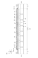
- FIG. 1 is a plan view showing a semiconductor device according to a first embodiment.
- FIG. 2 is a cross-sectional view taken along the line II-II shown in FIG.
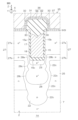
- FIG. 3 is a plan view showing an example of the layout of the first main surface.
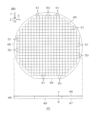
- FIG. 4 is an enlarged plan view showing an example of the layout of a main part of the first main surface.
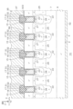
- FIG. 5 is a cross-sectional view taken along line V-V shown in FIG.
- FIG. 6 is a cross-sectional view taken along the line VI-VI shown in FIG.
- FIG. 7 is an enlarged cross-sectional view of a region including the gate structure shown in FIG.
- FIG. 8 is an enlarged cross-sectional view of a region including the gate structure shown in FIG. FIG.
- FIG. 10A is a cross-sectional view showing an example of a method for manufacturing a semiconductor device.
- FIG. 10B is a cross-sectional view showing a step subsequent to that of FIG. 10A.
- FIG. 10C is a cross-sectional view showing a step subsequent to FIG. 10B.
- FIG. 10D is a cross-sectional view showing a step subsequent to FIG. 10C.
- FIG. 10E is a cross-sectional view showing a step subsequent to FIG. 10D.
- FIG. 10F is a cross-sectional view showing a step subsequent to FIG. 10E.
- FIG. 10G is a cross-sectional view showing a step subsequent to FIG. 10F.
- FIG. 10A is a cross-sectional view showing an example of a method for manufacturing a semiconductor device.
- FIG. 10B is a cross-sectional view showing a step subsequent to that of FIG. 10A.
- FIG. 10C is a cross-sectional view showing a step subsequent to FIG
- FIG. 10H is a cross-sectional view showing a step subsequent to FIG. 10G.
- FIG. 10I is a cross-sectional view showing a step subsequent to FIG. 10H.
- FIG. 10J is a cross-sectional view showing a step subsequent to FIG. 10I.
- FIG. 10K is a cross-sectional view showing a step subsequent to FIG. 10J.
- FIG. 10L is a cross-sectional view showing a step subsequent to FIG. 10K.
- FIG. 10M is a cross-sectional view showing a step subsequent to FIG. 10L.
- FIG. 10N is a cross-sectional view showing a step subsequent to FIG. 10M.
- FIG. 10O is a cross-sectional view showing a step subsequent to FIG. 10N.
- FIG. 10N is a cross-sectional view showing a step subsequent to FIG. 10N.
- FIG. 10P is a cross-sectional view showing a step subsequent to that shown in FIG. 10O.
- FIG. 11 is a cross-sectional view showing a main part of a semiconductor device according to the second embodiment.
- FIG. 12 is a plan view showing a main part of a semiconductor device according to a third embodiment.
- 13 is a cross-sectional view taken along line XIII-XIII shown in FIG. 12.
- FIG. 14 is a cross-sectional view taken along line XIV-XIV shown in FIG. 12.
- FIG. 15 is an enlarged cross-sectional view of a region including the source structure shown in FIG.
- FIG. 16 is an enlarged cross-sectional view of the area including the source structure shown in FIG. FIG.
- FIG. 17 is a plan view showing a main part of a semiconductor device according to the fourth embodiment.
- FIG. 18 is a cross-sectional view showing a semiconductor device according to a first modification.
- FIG. 19 is a cross-sectional view showing a semiconductor device according to a second modification.
- FIG. 20 is a cross-sectional view showing a semiconductor device according to a third modification.
- FIG. 21 is a cross-sectional view showing a semiconductor device according to a fourth modification.
- FIG. 22 is a cross-sectional view showing a semiconductor device according to a fifth modification.
- FIG. 23 is a cross-sectional view showing a semiconductor device according to a sixth modification.
- FIG. 24 is a cross-sectional view showing a semiconductor device according to a seventh modification.
- FIG. 25 is a cross-sectional view showing a semiconductor device according to an eighth modification.
- this term includes a numerical value (shape) that is equal to the numerical value (shape) of the comparison target, as well as a numerical error (shape error) within a range of ⁇ 10% based on the numerical value (shape) of the comparison target.
- shape a numerical value that is equal to the numerical value (shape) of the comparison target
- error a numerical error within a range of ⁇ 10% based on the numerical value (shape) of the comparison target.
- the conductivity type of a semiconductor is indicated using “p-type” or “n-type”, but “p-type” may also be referred to as the “first conductivity type” and “n-type” as the “second conductivity type”. Of course, “n-type” may also be referred to as the "first conductivity type” and “p-type” as the “second conductivity type”.
- P-type is a conductivity type resulting from a trivalent element
- n-type is a conductivity type resulting from a pentavalent element.
- the trivalent element is at least one of boron, aluminum, gallium, and indium.
- the pentavalent element is at least one of nitrogen, phosphorus, arsenic, antimony, and bismuth.
- FIG. 1 is a plan view showing a semiconductor device 1A according to the first embodiment.
- FIG. 2 is a cross-sectional view taken along line II-II shown in FIG. 1.
- FIG. 3 is a plan view showing an example layout of the first main surface 3.
- FIG. 4 is an enlarged plan view showing an example layout of a major portion of the first main surface 3.
- FIG. 5 is a cross-sectional view taken along line V-V shown in FIG. 4.
- FIG. 6 is a cross-sectional view taken along line VI-VI shown in FIG. 4.
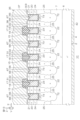
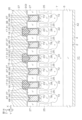
- FIG. 7 is an enlarged cross-sectional view of a region including the gate structure 15 shown in FIG. 5.
- FIG. 8 is an enlarged cross-sectional view of a region including the gate structure 15 shown in FIG. 6.
- semiconductor device 1A is a semiconductor switching device having an insulated gate type transistor structure Tr as an example of a device structure.
- the transistor structure Tr has a vertical structure.
- Semiconductor device 1A is a SiC semiconductor device having a chip 2 including a SiC single crystal. Chip 2 may be referred to as a "SiC chip” or a "semiconductor chip.”
- the chip 2 is made of hexagonal SiC single crystal and is formed into a rectangular parallelepiped shape.
- the hexagonal SiC single crystal has a number of polytypes including 2H (Hexagonal)-SiC single crystal, 4H-SiC single crystal, 6H-SiC single crystal, etc.
- the chip 2 is made of 4H-SiC single crystal, but the chip 2 may be made of other polytypes.
- the chip 2 has a first main surface 3 on one side, a second main surface 4 on the other side, and first to fourth side surfaces 5A to 5D connecting the first main surface 3 and the second main surface 4.
- the first main surface 3 and the second main surface 4 are formed in a quadrangular shape in a plan view seen from the vertical direction Z (hereinafter simply referred to as "plan view").
- the vertical direction Z is also the thickness direction of the chip 2 and the normal direction of the first main surface 3 (second main surface 4).
- the first main surface 3 and the second main surface 4 may be formed in a square or rectangular shape in a plan view.
- the first main surface 3 and the second main surface 4 are preferably formed by the c-plane of the SiC single crystal.
- the first main surface 3 is formed by the silicon surface ((0001) surface) of the SiC single crystal
- the second main surface 4 is formed by the carbon surface ((000-1) surface) of the SiC single crystal.
- the first side surface 5A and the second side surface 5B extend in a first direction X along the first main surface 3 and face a second direction Y that intersects with the first direction X along the first main surface 3. Specifically, the second direction Y is perpendicular to the first direction X.
- the third side surface 5C and the fourth side surface 5D extend in the second direction Y and face the first direction X.
- the first direction X is the m-axis direction ([1-100] direction) of the SiC single crystal
- the second direction Y is the a-axis direction ([11-20] direction) of the SiC single crystal.
- the first direction X may be the a-axis direction of the SiC single crystal
- the second direction Y may be the m-axis direction of the SiC single crystal.
- the direction extending along the first main surface 3 may be referred to as the "horizontal direction.”
- the horizontal direction is also the XY plane (horizontal plane) formed by the first direction X and the second direction Y, and is perpendicular to the vertical direction Z.
- the chip 2 (first main surface 3 and second main surface 4) has an off angle that is inclined at a predetermined angle in a predetermined off direction relative to the c-plane of the SiC single crystal.
- the c-axis ((0001) axis) of the SiC single crystal is inclined from the vertical line toward the off direction by the off angle.
- the c-plane of the SiC single crystal is inclined by the off angle relative to the horizontal plane.
- the off-direction is preferably the a-axis direction of the SiC single crystal (i.e., the second direction Y).
- the off-angle may be greater than 0° and less than or equal to 10°.
- the off-angle may have a value that falls within at least one of the following ranges: greater than 0° and less than or equal to 1°, 1° or more and less than or equal to 2.5°, 2.5° or more and less than or equal to 5°, 5° or more and less than or equal to 7.5°, and 7.5° or more and less than or equal to 10°.
- the off angle is preferably 5° or less. It is particularly preferable that the off angle be 2° or more and 4.5° or less.
- the off angle is typically set in the range of 4° ⁇ 0.1°. This specification does not exclude a configuration in which the off angle is 0° (i.e., a configuration in which the first main surface 3 is a just plane relative to the c-plane).
- the semiconductor device 1A includes an n-type first semiconductor region 6 formed in a surface layer portion of the second main surface 4 of the chip 2.
- a drain potential is applied to the first semiconductor region 6 as a first potential (high potential).
- the first semiconductor region 6 may be referred to as a "semiconductor layer", a “first semiconductor layer”, a “drain region”, or the like.
- the first semiconductor region 6 may have an n-type impurity concentration of 1 ⁇ 10 14 cm -3 or more and 1 ⁇ 10 21 cm -3 or less.
- the first semiconductor region 6 is formed in a layer extending along the second main surface 4, and is exposed from the second main surface 4 of the chip 2 and the first to fourth side surfaces 5A to 5D of the chip 2.
- the first semiconductor region 6 is made of an n-type semiconductor layer.
- the first semiconductor region 6 is made of a substrate (SiC substrate) containing SiC single crystal (semiconductor single crystal), and forms the second main surface 4 of the chip 2 and the first to fourth side surfaces 5A to 5D of the chip 2.
- the first semiconductor region 6 (substrate) has the off direction and off angle described above.
- the first semiconductor region 6 may have a thickness of 10 ⁇ m or more and 500 ⁇ m or less.
- the thickness of the first semiconductor region 6 may have a value that belongs to at least one of the following ranges: 10 ⁇ m or more and 50 ⁇ m or less, 50 ⁇ m or more and 100 ⁇ m or less, 100 ⁇ m or more and 150 ⁇ m or less, 150 ⁇ m or more and 200 ⁇ m or less, 200 ⁇ m or more and 300 ⁇ m or less, 300 ⁇ m or more and 400 ⁇ m or less, and 400 ⁇ m or more and 500 ⁇ m or less.
- the semiconductor device 1A includes an n-type second semiconductor region 7 formed in a surface layer portion of the first main surface 3 of the chip 2.
- the second semiconductor region 7 may be referred to as a "semiconductor layer,” a “second semiconductor layer,” a “drift region,” or the like.
- the second semiconductor region 7 has an n-type impurity concentration less than the n-type impurity concentration of the first semiconductor region 6.
- the n-type impurity concentration of the second semiconductor region 7 may be not less than 1 ⁇ 10 14 cm -3 and not more than 1 ⁇ 10 18 cm -3 .
- the second semiconductor region 7 is formed in a layer extending along the first main surface 3, and is electrically connected to the first semiconductor region 6.
- the second semiconductor region 7 is exposed from the second main surface 4 of the chip 2 and the first to fourth side surfaces 5A to 5D of the chip 2.
- the second semiconductor region 7 is made of an n-type semiconductor layer.
- the second semiconductor region 7 is made of an epitaxial layer (SiC epitaxial layer) containing SiC single crystal (semiconductor single crystal), and forms the first main surface 3 of the chip 2 and the first to fourth side surfaces 5A to 5D of the chip 2.
- the second semiconductor region 7 (epitaxial layer) has the off direction and off angle described above. It is preferable that the second semiconductor region 7 has a thickness less than the thickness of the first semiconductor region 6. The thickness of the second semiconductor region 7 may be greater than the thickness of the first semiconductor region 6.
- the thickness of the second semiconductor region 7 may be 5 ⁇ m or more and 50 ⁇ m or less.
- the thickness of the second semiconductor region 7 may have a value that belongs to at least one of the following ranges: 5 ⁇ m or more and 10 ⁇ m or less, 10 ⁇ m or more and 15 ⁇ m or less, 15 ⁇ m or more and 20 ⁇ m or less, 20 ⁇ m or more and 25 ⁇ m or less, 25 ⁇ m or more and 30 ⁇ m or less, 30 ⁇ m or more and 35 ⁇ m or less, 35 ⁇ m or more and 40 ⁇ m or less, 40 ⁇ m or more and 45 ⁇ m, and 45 ⁇ m or more and 50 ⁇ m or less.
- the semiconductor device 1A includes a first surface portion 8, a second surface portion 9, and first to fourth connection surface portions 10A to 10D formed on the first main surface 3.
- the first surface portion 8, the second surface portion 9, and the first to fourth connection surface portions 10A to 10D define a mesa 11 on the first main surface 3.
- the first surface portion 8, the second surface portion 9, and the first to fourth connection surface portions 10A to 10D may be considered to be components of the chip 2 (first main surface 3).
- the first surface portion 8 may be referred to as the "active surface”
- the second surface portion 9 may be referred to as the “outer surface”
- the first to fourth connecting surface portions 10A to 10D may be referred to as “connecting surfaces”
- the mesa 11 may be referred to as the "active mesa”.
- the first surface portion 8 is formed at a distance inward from the periphery (first to fourth side faces 5A to 5D) of the first main surface 3.
- the first surface portion 8 has a flat surface extending horizontally, and is formed by a c-plane (Si-plane).
- the first surface portion 8 is formed in a quadrangle shape having four sides parallel to the first to fourth side faces 5A to 5D in a plan view. It is preferable that the planar area of the first surface portion 8 is 50% to 90% of the planar area of the first main surface 3.
- the second surface portion 9 is located on the peripheral side of the first main surface 3 relative to the first surface portion 8, and is recessed from the height position of the first surface portion 8 in the thickness direction of the chip 2 (towards the second main surface 4).
- the second surface portion 9 extends in a band shape along the first surface portion 8 in a plan view, and is formed in a ring shape (specifically, a square ring shape) surrounding the first surface portion 8.
- the second surface portion 9 is connected to the first to fourth side surfaces 5A to 5D.
- the second surface 9 is formed approximately parallel to the first surface 8, and has a flat surface extending horizontally.
- the second surface 9 is formed by the c-plane (Si-plane).
- the second surface 9 is formed in the second semiconductor region 7 with a space therebetween from the first semiconductor region 6. In other words, the second surface 9 is recessed to a depth less than the thickness of the second semiconductor region 7, exposing the second semiconductor region 7.
- the second surface portion 9 has a depth of 0.1 ⁇ m or more and 3 ⁇ m or less.
- the depth of the second surface portion 9 may have a value that belongs to at least one of the following ranges: 0.1 ⁇ m or more and 0.5 ⁇ m or less, 0.5 ⁇ m or more and 1 ⁇ m or less, 1 ⁇ m or more and 1.5 ⁇ m or less, 1.5 ⁇ m or more and 2 ⁇ m or less, 2 ⁇ m or more and 2.5 ⁇ m or less, and 2.5 ⁇ m or more and 3 ⁇ m or less.
- the depth of the second surface portion 9 is preferably 1.5 ⁇ m or more and 2.5 ⁇ m or less.
- the first to fourth connection surface portions 10A to 10D extend in the vertical direction Z and are connected to the first surface portion 8 and the second surface portion 9.
- the first connection surface portion 10A is located on the first side surface 5A side
- the second connection surface portion 10B is located on the second side surface 5B side
- the third connection surface portion 10C is located on the third side surface 5C side
- the fourth connection surface portion 10D is located on the fourth side surface 5D side.
- the first connection surface portion 10A and the second connection surface portion 10B extend in the first direction X and face the second direction Y.
- the third connection surface portion 10C and the fourth connection surface portion 10D extend in the second direction Y and face the first direction X.
- the first to fourth connection surface portions 10A to 10D may extend almost vertically between the first surface portion 8 and the second surface portion 9, and define a mesa 11 in the shape of a rectangular prism.
- the first to fourth connection surface portions 10A to 10D may be inclined obliquely downward from the first surface portion 8 toward the second surface portion 9, and define a mesa 11 in the shape of a truncated rectangular pyramid.
- the first to fourth connection surface portions 10A to 10D may be inclined at an angle of more than 90° and not more than 135° with respect to the first surface portion 8.
- the mesa 11 is defined in a protruding shape in the second semiconductor region 7 on the first main surface 3.
- the mesa 11 is formed only in the second semiconductor region 7, and is not formed in the first semiconductor region 6.
- the semiconductor device 1A includes an active region 12 set in the chip 2.
- the active region 12 includes a device structure (transistor structure Tr) and is a region where an output current (drain current) is generated.
- the active region 12 is set in the inner part of the chip 2. Specifically, the active region 12 is set in the first surface portion 8.
- the semiconductor device 1A includes a peripheral region 13 that is set outside the active region 12 in the chip 2.
- the peripheral region 13 is a region that does not include a device structure (transistor structure Tr).
- the peripheral region 13 is set on the periphery of the chip 2.
- the peripheral region 13 is set on the second surface 9.
- the peripheral region 13 is set in the region between the periphery of the first surface 8 and the periphery of the second surface 9 in a plan view.
- the semiconductor device 1A includes a plurality of trench-type (trench electrode-type) gate structures 15 formed on the first main surface 3 (first surface portion 8).
- the gate structures 15 may be referred to as “trench gate structures", “trench structures”, etc.
- a gate potential is applied to the plurality of gate structures 15 as a control potential.
- the multiple gate structures 15 are formed on the first surface portion 8 at intervals inward from the periphery of the first surface portion 8 (first to fourth connection surface portions 10A to 10D).
- the multiple gate structures 15 are arranged at intervals in the first direction X in a plan view, and are each formed in a band shape extending in the second direction Y. In other words, the multiple gate structures 15 are arranged in stripes extending in the second direction Y in a plan view.
- the multiple gate structures 15 may be arranged with an interval of 0.25 ⁇ m or more and 3 ⁇ m or less.
- the interval between the gate structures 15 may have a value that belongs to at least one of the following ranges: 0.25 ⁇ m or more and 0.5 ⁇ m or less, 0.5 ⁇ m or more and 0.75 ⁇ m or less, 0.75 ⁇ m or more and 1 ⁇ m or less, 1 ⁇ m or more and 1.25 ⁇ m or less, 1.25 ⁇ m or more and 1.5 ⁇ m or less, 1.5 ⁇ m or more and 1.75 ⁇ m or less, 1.75 ⁇ m or more and 2 ⁇ m or less, 2 ⁇ m or more and 2.25 ⁇ m or less, 2.25 ⁇ m or more and 2.5 ⁇ m or less, 2.5 ⁇ m or more and 2.75 ⁇ m or less, and 2.75 ⁇ m or more and 3 ⁇ m or less.
- the interval between the gate structures 15 is preferably 0.5 ⁇ m or more and 1.5 ⁇ m or less.
- the multiple gate structures 15 are located within the second semiconductor region 7.
- the multiple gate structures 15 are formed at intervals from the bottom of the second semiconductor region 7 toward the first main surface 3, and face the first semiconductor region 6 across a portion of the second semiconductor region 7.
- the multiple gate structures 15 are formed approximately perpendicular to the first main surface 3 (first surface portion 8).
- each of the gate structures 15 has a first side wall 15a on one side in the first direction X (the third side surface 5C side), a second side wall 15b on the other side in the first direction X (the fourth side surface 5D side), and a bottom wall 15c connecting the first side wall 15a and the second side wall 15b.
- the first sidewall 15a and the second sidewall 15b are each formed by the a-plane ((11-20) plane) of the SiC single crystal.
- the first sidewall 15a and the second sidewall 15b may each be formed by the m-plane ((1-100) plane) of the SiC single crystal depending on the extension direction of the gate structure 15.
- the first sidewall 15a and the second sidewall 15b are formed approximately perpendicular to the first main surface 3.
- the inclination angle (absolute value) of the first side wall 15a (second side wall 15b) based on the vertical line may be 85° or more and 95° or less.
- the inclination angle of the first side wall 15a (second side wall 15b) may have a value that belongs to at least one of the ranges of 85° or more and 87.5° or less, 87.5° or more and 90° or less, 90° or more and 92.5° or less, and 92.5° or more and 95° or less.
- the inclination angle of the first side wall 15a (second side wall 15b) is preferably 87° or more and 93° or less.
- the bottom wall 15c is formed by the c-plane (Si-plane) of the SiC single crystal. It is preferable that the bottom wall 15c extends almost flat along the horizontal direction. Of course, the bottom wall 15c may be curved in an arc shape toward the second main surface 4.
- the gate structure 15 may have a width of 0.1 ⁇ m or more and 1.5 ⁇ m or less.
- the width of the gate structure 15 may have a value that belongs to at least one of the following ranges: 0.1 ⁇ m or more and 0.25 ⁇ m or less, 0.25 ⁇ m or more and 0.5 ⁇ m or less, 0.5 ⁇ m or more and 0.75 ⁇ m or less, 0.75 ⁇ m or more and 1 ⁇ m or less, 1 ⁇ m or more and 1.25 ⁇ m or less, and 1.25 ⁇ m or more and 1.5 ⁇ m or less.
- the width of the gate structure 15 is preferably 0.25 ⁇ m or more and 0.75 ⁇ m or less.
- the gate structure 15 may have a depth of 0.1 ⁇ m or more and 3 ⁇ m or less.
- the depth of the gate structure 15 may have a value that belongs to at least one of the following ranges: 0.1 ⁇ m or more and 0.5 ⁇ m or less, 0.5 ⁇ m or more and 1 ⁇ m or less, 1 ⁇ m or more and 1.5 ⁇ m or less, 1.5 ⁇ m or more and 2 ⁇ m or less, 2 ⁇ m or more and 2.5 ⁇ m or less, and 2.5 ⁇ m or more and 3 ⁇ m or less.
- the depth of the gate structure 15 is preferably 0.5 ⁇ m or more and 1.5 ⁇ m or less.
- the depth of the gate structure 15 is preferably approximately equal to the depth of the second surface portion 9.
- Each of the multiple gate structures 15 includes a trench 16, an insulating film 17, and a buried electrode 18.
- the trench 16 is formed in the first main surface 3 (first surface portion 8) and defines the walls of the gate structure 15 (first sidewall 15a, second sidewall 15b, and bottom wall 15c).
- the insulating film 17 may include at least one of a silicon oxide film, a silicon nitride film, and a silicon oxynitride film.
- the insulating film 17 has a single-layer structure made of a silicon oxide film. It is particularly preferable that the insulating film 17 includes a silicon oxide film made of an oxide of the chip 2.
- the insulating film 17 coats the wall surface of the trench 16 in a film-like manner.
- the insulating film 17 includes a first film portion, a second film portion, and a third film portion.
- the first film portion coats the first side wall 15a in a film-like manner.
- the second film portion coats the second side wall 15b in a film-like manner.
- the third film portion coats the bottom wall 15c in a film-like manner, and is connected to the first film portion and the second film portion.
- the second membrane portion has a thickness approximately equal to that of the first membrane portion.
- the third membrane portion has a thickness greater than both the thickness of the first membrane portion and the thickness of the second membrane portion.
- the thickness of the third membrane portion may be approximately equal to the thickness of the first membrane portion and the thickness of the second membrane portion.
- the insulating film 17 may have a thickness of 10 nm or more and 150 nm or less.
- the thickness of the insulating film 17 may have a value that belongs to at least one of the following ranges: 10 nm or more and 25 nm or less, 25 nm or more and 50 nm or less, 50 nm or more and 75 nm or less, 75 nm or more and 100 nm or less, 100 nm or more and 125 nm or less, and 125 nm or more and 150 nm or less.
- the buried electrode 18 may contain either or both of p-type conductive polysilicon and n-type conductive polysilicon.
- the buried electrode 18 is buried in the trench 16 with the insulating film 17 sandwiched therebetween.
- the buried electrode 18 has an electrode surface exposed from the trench 16.
- the electrode surface is located on the bottom wall 15c side relative to the height position of the first main surface 3.
- the electrode surface has a recess in its inner part that tapers toward the bottom wall 15c side. It is preferable that the bottom of the recess is located on the first main surface 3 side relative to the depth position of the middle part of the trench 16.
- the semiconductor device 1A includes a plurality of p-type body regions 20 formed in a surface layer portion of the first main surface 3 (first surface portion 8).
- a source potential is applied to the plurality of body regions 20 as a second potential (low potential) different from a first potential (high potential).
- the body regions 20 may be referred to as a "channel region", a "base region”, or the like.
- the plurality of body regions 20 may have a p-type impurity concentration of 1 ⁇ 10 17 cm -3 or more and 1 ⁇ 10 19 cm -3 or less.
- the multiple body regions 20 are formed in regions along the multiple gate structures 15. Specifically, the multiple body regions 20 are formed in regions between the multiple gate structures 15, and extend in stripes along the multiple gate structures 15.
- the body region 20 is formed in a layer extending in the first direction X in a cross-sectional view, and is connected to one or both (both in this embodiment) of the multiple adjacent gate structures 15.
- the body region 20 faces the buried electrodes 18 of the multiple gate structures 15, with the insulating films 17 of the multiple gate structures 15 sandwiched therebetween.
- the body region 20 is formed at a distance from the depth position of the second surface 9 to the region on the first surface 8 side.
- the body region 20 is formed at a distance from the depth position of the bottom wall 15c of the gate structure 15 to the first main surface 3 side.
- the body region 20 has a bottom located on the bottom wall 15c side of the gate structure 15 with respect to the depth position of the middle part of the gate structure 15.
- the bottom of the body region 20 is located in the region between the bottom wall 15c of the gate structure 15 and the middle part of the gate structure 15. In other words, the distance between the bottom of the body region 20 and the bottom wall 15c of the gate structure 15 is less than the thickness (depth) of the body region 20.
- the bottom of the body region 20 is located on the bottom wall 15c side of the gate structure 15 with respect to the bottom of the recess of the buried electrode 18.
- the bottom of the body region 20 may be located on the first main surface 3 side with respect to the depth position of the middle part of the gate structure 15.
- the body region 20 may have a thickness of 0.1 ⁇ m or more and 1 ⁇ m or less.
- the thickness of the body region 20 may have a value that belongs to at least one of the following ranges: 0.1 ⁇ m or more and 0.2 ⁇ m or less, 0.2 ⁇ m or more and 0.4 ⁇ m or less, 0.4 ⁇ m or more and 0.6 ⁇ m or less, 0.6 ⁇ m or more and 0.8 ⁇ m or less, and 0.8 ⁇ m or more and 1 ⁇ m or less.
- the thickness of the body region 20 is preferably 0.3 ⁇ m or more and 0.7 ⁇ m or less.
- the semiconductor device 1A includes a plurality of n-type source regions 21 formed in a region on the first main surface 3 side with respect to the plurality of body regions 20.
- the plurality of source regions 21 have an n-type impurity concentration higher than the n-type impurity concentration of the second semiconductor region 7.
- the n-type impurity concentration of the plurality of source regions 21 may be not less than 1 ⁇ 10 18 cm ⁇ 3 and not more than 1 ⁇ 10 21 cm ⁇ 3 .
- the multiple source regions 21 are formed in regions along the multiple gate structures 15 in the surface layer of the multiple body regions 20. Specifically, the multiple source regions 21 are formed in regions between the multiple gate structures 15, and extend in stripes along the multiple gate structures 15.
- the configuration of one source region 21 will be described below.
- the source region 21 is formed at a distance from the bottom of the body region 20 toward the first main surface 3.
- the source region 21 is formed in a layer extending in the first direction X in a cross-sectional view, and is connected to one or both (both in this embodiment) of the adjacent gate structures 15.
- the source region 21 faces the buried electrodes 18 of the gate structures 15 with the insulating films 17 of the gate structures 15 in between.
- the source region 21 has a bottom portion located on the bottom wall 15c side of the trench 16 relative to the height position of the electrode surface of the buried electrode 18, and a surface portion located on the first main surface 3 side relative to the height position of the electrode surface of the buried electrode 18.
- the source region 21 has a portion (bottom portion) that faces the buried electrode 18 across the insulating film 17, and a portion (surface portion) that does not face the buried electrode 18 across the insulating film 17.
- the bottom of the source region 21 may be located on the first main surface 3 side relative to the depth position of the bottom of the recess of the buried electrode 18.
- the bottom of the source region 21 may be located on the bottom side of the body region 20 relative to the depth position of the bottom of the recess.
- the semiconductor device 1A includes a plurality of p-type well regions 22 formed in the chip 2 (second semiconductor region 7).
- the plurality of well regions 22 have a p-type impurity concentration higher than the p-type impurity concentration of the body region 20.
- the p-type impurity concentration of the plurality of well regions 22 may be lower than the p-type impurity concentration of the body region 20.
- the p-type impurity concentration of the plurality of well regions 22 may be not less than 1 ⁇ 10 16 cm ⁇ 3 and not more than 1 ⁇ 10 20 cm ⁇ 3 .
- the multiple well regions 22 are formed in the chip 2 (second semiconductor region 7) in regions along the bottom walls 15c of the multiple gate structures 15 at intervals in the first direction X.
- the multiple well regions 22 are formed in a one-to-one correspondence with the multiple gate structures 15.
- the multiple well regions 22 are each formed in a strip shape extending along the corresponding gate structure 15 in a plan view, and face the corresponding buried electrode 18 across the corresponding insulating film 17.
- multiple well regions 22 may be formed in a one-to-many correspondence with one gate structure 15. In this case, the multiple well regions 22 are formed at intervals in the second direction Y.
- the configuration of one well region 22 is described below.
- the well region 22 is formed to be wider than the gate structure 15 in a plan view.
- the well region 22 is formed in a columnar shape extending in the thickness direction (vertical direction Z) of the second semiconductor region 7 in a cross-sectional view.
- the well region 22 may have a depth that crosses the intermediate portion between the bottom of the second semiconductor region 7 and the bottom wall 15c of the gate structure 15.
- the well region 22 may be formed at a distance from the intermediate portion between the bottom of the second semiconductor region 7 and the bottom wall 15c of the gate structure 15 toward the first main surface 3.
- the well region 22 is formed at a distance from the bottom of the second semiconductor region 7 toward the first surface portion 8, and faces the first semiconductor region 6 across a portion of the second semiconductor region 7. Of course, the well region 22 may cross the bottom of the second semiconductor region 7 and have a bottom located within the first semiconductor region 6. The well region 22 forms a pn junction with the second semiconductor region 7.
- the well region 22 has a thickness (depth) greater than the thickness (depth) of the body region 20.
- the thickness of the well region 22 is the thickness of the well region 22 in the vertical direction Z based on the bottom wall 15c of the gate structure 15. In this embodiment, the thickness of the well region 22 is greater than the depth of the gate structure 15.
- the thickness of the well region 22 may be less than the depth of the gate structure 15. In this case, the thickness of the well region 22 may be less than the thickness of the body region 20.
- the well region 22 has an upper end that is aligned with the corner of the bottom wall 15c of the gate structure 15. At the upper end, the well region 22 has a first extension 22a on the first sidewall 15a side and a second extension 22b on the second sidewall 15b side (see FIG. 7).
- the first extension 22a is drawn out from the region directly below the gate structure 15 to the lower end of the first sidewall 15a.
- the first extension 22a is formed at a distance from the bottom of the body region 20 toward the bottom wall 15c of the gate structure 15.
- the first extension 22a faces the buried electrode 18 in the horizontal direction, sandwiching the insulating film 17 therebetween.
- the first extension 22a may be formed on the bottom wall 15c side of the trench 16 with respect to the depth position of the lower end of the buried electrode 18, and may face only the insulating film 17 (third film portion) in the horizontal direction.
- the first extension 22a is formed in a tapered shape toward the first main surface 3 (the bottom side of the body region 20) in a cross-sectional view.
- the second extension 22b is drawn out from the region directly below the gate structure 15 to the lower end of the second sidewall 15b, and faces the first extension 22a across the gate structure 15.
- the second extension 22b is formed at a distance from the bottom of the body region 20 toward the bottom wall 15c of the gate structure 15.
- the second extension 22b faces the buried electrode 18 in the horizontal direction, with the insulating film 17 in between.
- the second extension 22b may be formed on the bottom wall 15c side of the trench 16 with respect to the depth position of the lower end of the buried electrode 18, and may face only the insulating film 17 (third film portion) in the horizontal direction.
- the second extension 22b is formed in a tapered shape toward the first main surface 3 (the bottom side of the body region 20) in a cross-sectional view.
- the well region 22 has one or more (multiple in this embodiment) first bulge portions 22c.
- first bulge portions 22c In the attached drawings, a well region 22 having four first bulge portions 22c is illustrated as an example. The number of first bulge portions 22c is adjusted appropriately by adjusting the process conditions.
- the multiple first bulge portions 22c are each formed by a portion of the well region 22 whose width in the horizontal direction (first direction X) gradually increases and decreases in the thickness direction, and are formed in multiple stages from the bottom wall 15c of the gate structure 15 toward the bottom of the second semiconductor region 7.
- the multiple first bulges 22c extend in an arc shape (circular arc) from the region directly below the gate structure 15 to both sides of the gate structure 15.
- the single first bulge 22c may be formed in the middle of the well region 22 so as to extend in an arc shape (circular arc) to both sides of the gate structure 15.
- the semiconductor device 1A includes a plurality of p-type high-concentration well regions 23 formed in each of the plurality of well regions 22.
- the plurality of high-concentration well regions 23 are regions in which the p-type impurity concentration of the well region 22 is increased, and have a p-type impurity concentration higher than the p-type impurity concentration of the well region 22.
- the high-concentration well regions 23 may be regarded as a high-concentration portion of the well region 22.
- the p-type impurity concentration of the plurality of high-concentration well regions 23 may be not less than 1 ⁇ 10 18 cm ⁇ 3 and not more than 1 ⁇ 10 20 cm ⁇ 3 .
- the multiple high-concentration well regions 23 are formed in a one-to-one correspondence with the multiple well regions 22.
- the multiple high-concentration well regions 23 are each formed in a region along the bottom wall 15c of the corresponding gate structure 15.
- the multiple high-concentration well regions 23 are each formed in a strip shape extending along the corresponding gate structure 15 (well region 22) in a plan view, and face the corresponding buried electrode 18 with the corresponding insulating film 17 in between.
- multiple high-concentration well regions 23 may be formed in a one-to-many correspondence with one well region 22.
- the multiple high-concentration well regions 23 are formed at intervals in the second direction Y within one well region 22.
- the configuration of one high-concentration well region 23 is described below.
- the high-concentration well region 23 is formed at a distance from the bottom of the well region 22 toward the bottom wall 15c of the gate structure 15. It is preferable that the high-concentration well region 23 has a bottom located toward the bottom wall 15c of the gate structure 15 with respect to the depth position of the middle part of the well region 22.
- the bottom of the high-concentration well region 23 is defined by a concentration transition portion where the p-type impurity concentration gradually decreases toward the bottom side of the well region 22.
- the bottom of the high-concentration well region 23 may be located on the bottom side of the well region 22 with respect to the depth position of the middle part of the well region 22.
- the high-concentration well region 23 is formed narrower than the well region 22.
- the high-concentration well region 23 is formed narrower than the gate structure 15.
- the high-concentration well region 23 may be formed wider than the gate structure 15 and extend out on both sides of the gate structure 15.
- the high-concentration well region 23 has a thickness (depth) less than the depth of the gate structure 15.
- the thickness of the high-concentration well region 23 is the thickness in the vertical direction Z of the high-concentration well region 23 based on the bottom wall 15c of the gate structure 15.
- the thickness of the high-concentration well region 23 is less than the thickness of the body region 20.
- the thickness of the high-concentration well region 23 may be greater than the thickness of the body region 20 or greater than the depth of the gate structure 15.
- the semiconductor device 1A includes a plurality of n-type high concentration regions 24 formed in the chip 2 (second semiconductor region 7) in regions below the plurality of body regions 20.
- the plurality of high concentration regions 24 are regions (low resistance regions) in which the n-type impurity concentration of the second semiconductor region 7 is increased, and have a higher n-type impurity concentration than the n-type impurity concentration of the second semiconductor region 7.
- the plurality of high concentration regions 24 may be regarded as high concentration portions of the second semiconductor region 7.
- the n-type impurity concentration of the multiple high concentration regions 24 may be not less than 1 ⁇ 10 16 cm ⁇ 3 and not more than 1 ⁇ 10 19 cm ⁇ 3 .
- the n-type impurity concentration of the multiple high concentration regions 24 can be appropriately compared by comparing it with the n-type impurity concentration on the bottom side of the second semiconductor region 7.
- the high concentration region 24 may be referred to as a “high concentration drift region”.
- the multiple high concentration regions 24 are formed in the regions below the multiple body regions 20 and along the multiple gate structures 15. Specifically, the multiple high concentration regions 24 are formed in the regions between the multiple gate structures 15 in the thickness range between the bottom walls 15c of the multiple gate structures 15 and the bottoms of the multiple body regions 20. The multiple high concentration regions 24 each extend in a band shape along the multiple gate structures 15 in a plan view.
- the high concentration region 24 is formed in a layer extending in the first direction X in a cross-sectional view, and is connected to one or both (both in this embodiment) of the multiple adjacent gate structures 15.
- the high concentration region 24 faces the buried electrodes 18 of the multiple gate structures 15, sandwiching the insulating films 17 of the multiple gate structures 15 therebetween.
- the high concentration region 24 faces the source region 21 in the thickness direction, sandwiching a portion of the body region 20 therebetween.
- the high concentration region 24 faces the source region 21 in a one-to-one correspondence in the thickness direction.
- the high concentration region 24 is formed at a distance from the bottom of the second semiconductor region 7 toward the first main surface 3, and faces the first semiconductor region 6 across a portion of the second semiconductor region 7. It is preferable that the high concentration region 24 is formed at a distance from the middle of the second semiconductor region 7 toward the first main surface 3.
- the high concentration region 24 has a bottom located on the first main surface 3 side relative to the depth position of the bottom wall 15c of the gate structure 15.
- the bottom of the high concentration region 24 is defined by a concentration transition section where the n-type impurity concentration gradually decreases toward the bottom side of the second semiconductor region 7.
- the high concentration region 24 is formed at a distance from the depth position of the bottom wall 15c of the gate structure 15 toward the first main surface 3.
- the high concentration region 24 is formed in a thickness range between the body region 20 and the well region 22, and separates the well region 22 from the body region 20. In other words, the high concentration region 24 suppresses an increase in the p-type impurity concentration in the portion along the sidewall (first sidewall 15a and second sidewall 15b) of the gate structure 15.
- the high concentration region 24 has a thickness (depth) in the vertical direction Z that is less than the thickness (depth) of the body region 20.
- the thickness of the high concentration region 24 may be 0.1 ⁇ m or more and 0.5 ⁇ m or less.
- the thickness of the high concentration region 24 may have a value that belongs to at least one of the following ranges: 0.1 ⁇ m or more and 0.15 ⁇ m or less, 0.15 ⁇ m or more and 0.2 ⁇ m or less, 0.2 ⁇ m or more and 0.25 ⁇ m or less, 0.25 ⁇ m or more and 0.3 ⁇ m or less, 0.3 ⁇ m or more and 0.35 ⁇ m or less, 0.35 ⁇ m or more and 0.4 ⁇ m or less, 0.4 ⁇ m or more and 0.45 ⁇ m or less, and 0.45 ⁇ m or more and 0.5 ⁇ m or less.
- the thickness of the high concentration region 24 is preferably 0.1 ⁇ m or more and 0.3 ⁇ m or less.
- the distance in the vertical direction Z between the bottom wall 15c of the gate structure 15 and the bottom of the high concentration region 24 may be 0 ⁇ m or more and 0.4 ⁇ m or less.
- the distance may have a value that belongs to at least one of the following ranges: 0 ⁇ m or more and 0.05 ⁇ m or less, 0.05 ⁇ m or more and 0.1 ⁇ m or less, 0.1 ⁇ m or more and 0.15 ⁇ m or less, 0.15 ⁇ m or more and 0.2 ⁇ m or less, 0.2 ⁇ m or more and 0.25 ⁇ m or less, 0.25 ⁇ m or more and 0.3 ⁇ m or less, 0.3 ⁇ m or more and 0.35 ⁇ m or less, and 0.35 ⁇ m or more and 0.4 ⁇ m or less.
- the distance is preferably 0.05 ⁇ m or more and 0.2 ⁇ m or less.
- the bottom of the high concentration region 24 may be located on the bottom side of the second semiconductor region 7 relative to the bottom wall 15c of the gate structure 15.
- the current density in the vicinity of the bottom wall 15c of the gate structure 15 is increased, and attention must be paid to electric field concentration in the vicinity of the bottom wall 15c of the gate structure 15 (especially in the vicinity of the corners of the bottom wall 15c).
- the multiple high concentration regions 24 may have approximately the same n-type impurity concentration, or may have different n-type impurity concentrations.
- the n-type impurity concentration of the other high concentration region 24 may be different from the n-type impurity concentration of the one high concentration region 24.
- the n-type impurity concentration of the other high concentration region 24 may be higher than the n-type impurity concentration of the one high concentration region 24, or may be lower than the n-type impurity concentration of the one high concentration region 24.
- the semiconductor device 1A includes a plurality of n-type medium concentration regions 25 formed in the chip 2 (second semiconductor region 7) in a region below a plurality of high concentration regions 24.
- the plurality of medium concentration regions 25 are regions (low resistance regions) in which the n-type impurity concentration of the second semiconductor region 7 is increased, and have an n-type impurity concentration that is higher than the n-type impurity concentration of the second semiconductor region 7 and lower than the n-type impurity concentration of the high concentration region 24.
- the plurality of medium concentration regions 25 may be regarded as high concentration portions of the second semiconductor region 7.
- the n-type impurity concentration of the plurality of medium concentration regions 25 may be not less than 1 ⁇ 10 15 cm ⁇ 3 and not more than 1 ⁇ 10 17 cm ⁇ 3 .
- the n-type impurity concentration of the plurality of medium concentration regions 25 can be appropriately compared by comparing it with the n-type impurity concentration on the bottom side of the second semiconductor region 7.
- the medium concentration region 25 may be referred to as a “medium concentration drift region”.
- the multiple medium concentration regions 25 are each formed in a thickness range between the bottom of the second semiconductor region 7 and the bottom of the multiple high concentration regions 24 in the region between the multiple gate structures 15.
- the multiple medium concentration regions 25 each have a portion interposed in the region between the multiple well regions 22.
- the multiple medium concentration regions 25 each have a portion interposed in the region of the multiple gate structures 15.
- the multiple medium concentration regions 25 each extend in a strip shape along the multiple gate structures 15 in a plan view.
- the multiple medium concentration regions 25 are connected to one or both (in this embodiment, both) of two adjacent well regions 22.
- the configuration of one medium concentration region 25 is described below.
- the medium concentration region 25 is formed at a distance from the bottom of the second semiconductor region 7 toward the first main surface 3, and faces the first semiconductor region 6 across a portion of the second semiconductor region 7.
- the medium concentration region 25 has an upper end located above the depth position of the bottom wall 15c of the gate structure 15.
- the upper end of the medium concentration region 25 is located in a region between multiple gate structures 15 and faces the gate structure 15 across the upper end (first extension 22a and second extension 22b) of the well region 22.
- the upper end of the medium concentration region 25 may have a portion connected to the gate structure 15.
- the medium concentration region 25 has a bottom that is located below the depth position of the bottom wall 15c of the gate structure 15. Specifically, the bottom of the medium concentration region 25 is formed at a distance from the bottom of the well region 22 toward the first main surface 3. It is preferable that the bottom of the medium concentration region 25 is located closer to the bottom of the well region 22 than the bottom of the high concentration well region 23.
- the bottom of the medium concentration region 25 may be located closer to the bottom of the second semiconductor region 7 than the middle part of the well region 22.
- the bottom of the medium concentration region 25 may be located closer to the bottom wall 15c of the gate structure 15 than the middle part of the well region 22.
- the semiconductor device 1A includes a plurality of channel regions 26 formed between the plurality of source regions 21 and the plurality of high concentration regions 24 in the plurality of body regions 20.
- the inversion and non-inversion of the plurality of channel regions 26 is controlled by the gate structure 15.
- the plurality of channel regions 26 form current paths connecting the plurality of source regions 21 and the plurality of high concentration regions 24 along the sidewalls (first sidewall 15a and second sidewall 15b) of the plurality of gate structures 15 in the plurality of body regions 20.
- the semiconductor device 1A includes a plurality of p-type first contact regions 27 formed in regions along the plurality of gate structures 15 in the surface layer portion of the first main surface 3 (first surface portion 8).
- the multiple first contact regions 27 have a p-type impurity concentration higher than the p-type impurity concentration of the multiple body regions 20.
- the p-type impurity concentration of the multiple first contact regions 27 is higher than the p-type impurity concentration of the multiple well regions 22.
- the p-type impurity concentration of the multiple first contact regions 27 may be not less than 1 ⁇ 10 17 cm ⁇ 3 and not more than 1 ⁇ 10 19 cm ⁇ 3 .
- the multiple first contact regions 27 are formed in the regions between the multiple gate structures 15. That is, the multiple first contact regions 27 are formed on both sides of the multiple gate structures 15.
- the multiple first contact regions 27 are arranged at intervals in the second direction Y along the multiple gate structures 15, and are each formed in a strip shape extending in the second direction Y.
- the multiple first contact regions 27 overlap the multiple body regions 20, increasing the p-type impurity concentration of the multiple body regions 20.
- the other first contact region 27 faces the first contact region 27 across the gate structure 15.
- the multiple first contact regions 27 are arranged in a matrix as a whole in a plan view.
- the length and spacing of the multiple first contact regions 27 are adjusted appropriately according to the channel area to be achieved.
- the channel area corresponds to the total area of the multiple source regions 21.
- the length of the first contact regions 27 in the second direction Y may be greater than the width of the gate structure 15 in the first direction X.
- the length of the first contact regions 27 may be less than the width of the gate structure 15.
- the first ratio of the length of the first contact region 27 to the width of the gate structure 15 may be 0.5 or more and 10 or less.
- the first ratio may have a value that belongs to at least one of the following ranges: 0.5 or more and 1 or less, 1 or more and 2.5 or less, 2.5 or more and 5 or less, 5 or more and 7.5 or less, and 7.5 or more and 10 or less.
- the first ratio is preferably 1 or more and 5 or less.
- the second ratio of the spacing of the first contact regions 27 to the length of the first contact regions 27 may be 1 or more and 50 or less.
- the second ratio may have a value that belongs to at least one of the following ranges: 1 or more and 5 or less, 5 or more and 10 or less, 10 or more and 15 or less, 15 or more and 20 or less, 20 or more and 25 or less, 25 or more and 30 or less, 30 or more and 35 or less, 35 or more and 40 or less, 40 or more and 45 or less, and 45 or more and 50 or less.
- the configuration of one first contact region 27 will be described below.
- the first contact region 27 is formed in a layer extending horizontally along the first main surface 3, and is connected to one or both (in this embodiment, both) of the adjacent gate structures 15.
- the first contact region 27 faces the buried electrodes 18 of the multiple gate structures 15, sandwiching the insulating films 17 of the multiple gate structures 15 therebetween.
- the first contact region 27 has a thickness greater than the thickness of the source region 21, and has a bottom located closer to the bottom of the second semiconductor region 7 than the bottom of the source region 21.
- the bottom of the first contact region 27 is located closer to the bottom of the body region 20 than the depth position of the bottom of the recess of the buried electrode 18.
- the first contact region 27 has a thickness greater than the thickness of the body region 20, and has a bottom located closer to the bottom of the second semiconductor region 7 than the bottom of the body region 20.
- the bottom of the first contact region 27 is defined by a concentration transition portion where the p-type impurity concentration gradually decreases toward the bottom of the second semiconductor region 7.
- the bottom of the first contact region 27 may be located closer to the first major surface 3 than the depth position of the bottom wall 15c of the gate structure 15.
- the first contact region 27 may have a thickness less than the thickness of the body region 20, and may have a bottom located closer to the first major surface 3 than the bottom of the body region 20.
- the first contact region 27 may face the high concentration region 24 across a portion of the body region 20.
- the bottom of the first contact region 27 is located closer to the bottom of the second semiconductor region 7 than the depth position of the bottom wall 15c of the gate structure 15.
- the first contact region 27 overlaps part or all of the high concentration region 24 in a cross-sectional view.
- the first contact region 27 replaces the n-type impurity concentration of part or all of the high concentration region 24 with a p-type impurity concentration. Therefore, the p-type impurity concentration at the bottom (lower end) of the first contact region 27 is reduced by the amount of the n-type impurity concentration of the high concentration region 24.
- the first contact region 27 has a bottom that crosses the bottom of the high concentration region 24 and is located within the medium concentration region 25. Therefore, the first contact region 27 also replaces the n-type impurity concentration of a portion of the medium concentration region 25 with a p-type impurity concentration. It is preferable that the bottom of the first contact region 27 is located closer to the first main surface 3 than the depth position of the middle part of the well region 22.
- the bottom of the first contact region 27 overlaps with the upper end of the well region 22 (first extension 22a and second extension 22b) in a region closer to the bottom of the second semiconductor region 7 than the depth position of the bottom wall 15c of the gate structure 15. As a result, the first contact region 27 electrically connects the well region 22 to the body region 20.
- the first contact region 27 has a high concentration portion 27a on the first main surface 3 side and a low concentration portion 27b on the bottom side of the second semiconductor region 7.
- the high concentration portion 27a is formed at least closer to the first main surface 3 than the depth position of the bottom wall 15c of the gate structure 15, and forms the main body of the first contact region 27.
- the high concentration portion 27a extends horizontally in a layer along the first main surface 3.
- the low concentration portion 27b is formed on the bottom side of the second semiconductor region 7 relative to the high concentration portion 27a, and forms the bottom (concentration transition portion) of the first contact region 27.
- the low concentration portion 27b is also a portion where the p-type impurity concentration is reduced by the n-type impurity concentration of the high concentration region 24.
- the low concentration portion 27b has a thickness less than the thickness of the high concentration portion 27a, and extends horizontally in a layer along the high concentration portion 27a.
- the low concentration portion 27b crosses the depth position of the bottom wall 15c of the gate structure 15 in the thickness direction.
- the low concentration portion 27b has a portion located closer to the first main surface 3 than the depth position of the bottom wall 15c of the gate structure 15, and a portion located closer to the bottom of the second semiconductor region 7 than the depth position of the bottom wall 15c of the gate structure 15.
- the low concentration portion 27b overlaps the upper ends of the multiple well regions 22 and is electrically connected to the multiple well regions 22.
- the low concentration portion 27b may be located only on the first main surface 3 side from the depth position of the bottom wall 15c of the gate structure 15 depending on the thickness of the high concentration portion 27a.
- the low concentration portion 27b may be located only on the bottom side of the second semiconductor region 7 from the depth position of the bottom wall 15c of the gate structure 15 depending on the thickness of the high concentration portion 27a.
- the semiconductor device 1A includes a plurality of p-type second contact regions 28 formed in regions along the bottom walls 15c of the plurality of gate structures 15 in the chip 2.
- the plurality of second contact regions 28 have a p-type impurity concentration higher than the p-type impurity concentration of the plurality of body regions 20.
- the p-type impurity concentration of the plurality of second contact regions 28 is higher than the p-type impurity concentration of the plurality of well regions 22.
- the p-type impurity concentration of the second contact regions 28 may be not less than 1 ⁇ 10 18 cm ⁇ 3 and not more than 1 ⁇ 10 20 cm ⁇ 3 .
- the p-type impurity concentration of the second contact regions 28 is preferably approximately equal to the p-type impurity concentration of the first contact regions 27.
- the second contact regions 28 are formed in a one-to-many correspondence with the bottom walls 15c of the gate structures 15.
- the second contact regions 28 are each interposed in the region between the first contact regions 27 adjacent to each other in the first direction X in a plan view. In other words, the second contact regions 28 are positioned on the same straight line as the first contact regions 27 in the first direction X.
- the second contact regions 28 are each formed in a band shape extending along the corresponding gate structure 15 in a plan view, and face the buried electrode 18 across the insulating film 17.
- the length of the second contact regions 28 is approximately equal to the length of the first contact regions 27.
- the spacing between the second contact regions 28 is approximately equal to the spacing between the first contact regions 27.
- the configuration of one second contact region 28 will be described below.
- the second contact region 28 is formed in one corresponding well region 22.
- the second contact region 28 overlaps with the high concentration well region 23 and is electrically connected to the high concentration well region 23 within the well region 22.
- the second contact region 28 is formed at a distance inward from the periphery of the well region 22.
- the second contact regions 28 are formed at a distance from the bottom of the well region 22 toward the bottom wall 15c of the gate structure 15, and face the bottom of the second semiconductor region 7 across a portion of the well region 22.
- the second contact regions 28 are each formed in a columnar shape extending in the thickness direction (vertical direction Z) of the second semiconductor region 7 in a cross-sectional view.
- the second contact region 28 has a bottom that is located closer to the bottom of the well region 22 than the thickness position of the middle part of the well region 22.
- the bottom of the second contact region 28 may be located closer to the bottom wall 15c of the gate structure 15 than the thickness position of the middle part of the well region 22.
- the bottom of the second contact region 28 is located closer to the bottom wall 15c of the gate structure 15 than the bottom of the medium concentration region 25.
- the bottom of the second contact region 28 may be located closer to the bottom of the second semiconductor region 7 than the bottom of the medium concentration region 25.
- the second contact region 28 may be formed to cross the bottom of the well region 22 and have a bottom located within the second semiconductor region 7.
- the second contact region 28 has an upper end that is aligned with a corner of the bottom wall 15c of the gate structure 15.
- the second contact region 28 is electrically connected to the multiple first contact regions 27 at its upper end.
- the second contact region 28 electrically connects the well region 22 and the high-concentration well region 23 to the body region 20 via the multiple first contact regions 27.
- the second contact region 28 has a first extension 28a on the first sidewall 15a side and a second extension 28b on the second sidewall 15b side.
- the first extension 28a is drawn out from the region directly below the gate structure 15 to the lower end of the first sidewall 15a.
- the first extension 28a faces the buried electrode 18 in the horizontal direction, sandwiching the insulating film 17 therebetween.
- the first extension 28a is connected to the first contact region 27 in a region along the first sidewall 15a. Specifically, the first extension 28a is connected to both the high concentration portion 27a and the low concentration portion 27b of the first contact region 27.
- the second extension 28b is drawn out from the region directly below the gate structure 15 to the lower end of the second sidewall 15b, and faces the first extension 28a across the gate structure 15.
- the second extension 28b faces the buried electrode 18 in the horizontal direction, across the insulating film 17.
- the second extension 28b is connected to the first contact region 27 in a region along the second sidewall 15b. Specifically, the second extension 28b is connected to both the high concentration portion 27a and the low concentration portion 27b of the first contact region 27.
- the second contact region 28 has one or more (multiple in this embodiment) second bulge portions 28c.
- a second contact region 28 having two second bulge portions 28c is illustrated as an example. The number of second bulge portions 28c is adjusted as appropriate by adjusting the process conditions.
- the multiple second bulges 28c are each formed by a portion of the second contact region 28 whose width in the horizontal direction (first direction X) gradually increases or decreases in the thickness direction, and are formed in multiple steps from the bottom wall 15c of the gate structure 15 toward the bottom of the second semiconductor region 7.
- the multiple second bulges 28c extend in an arc shape (circular arc) from the region directly below the gate structure 15 to both sides of the gate structure 15.
- the single second bulge 28c may be formed in the middle of the second contact region 28 so as to extend in an arc shape (circular arc) to both sides of the gate structure 15.
- the semiconductor device 1A includes a main surface insulating film 30 that covers the first main surface 3.
- the main surface insulating film 30 selectively covers the first surface portion 8, the second surface portion 9, and the first to fourth connection surface portions 10A to 10D.
- the main surface insulating film 30 is connected to the insulating films 17 of the multiple gate structures 15 on the first surface portion 8, and exposes the buried electrodes 18 of the multiple gate structures 15.
- the main surface insulating film 30 may include at least one of a silicon oxide film, a silicon nitride film, and a silicon oxynitride film.
- the main surface insulating film 30 has a single-layer structure made of a silicon oxide film. It is particularly preferable that the main surface insulating film 30 includes a silicon oxide film made of an oxide of the chip 2.
- the semiconductor device 1A includes an insulating interlayer film 31 that covers the main surface insulating film 30.
- the interlayer film 31 may be called an "insulating film,” an “interlayer insulating film,” an “intermediate insulating film,” or the like.
- the interlayer film 31 selectively covers the first surface portion 8, the second surface portion 9, and the first to fourth connection surface portions 10A to 10D, sandwiching the main surface insulating film 30 therebetween.
- the interlayer film 31 covers a plurality of gate structures 15 (buried electrodes 18) on the first surface portion 8.
- the interlayer film 31 is continuous with the first to fourth side faces 5A to 5D at the periphery of the second surface 9.
- the interlayer film 31 may be formed at a distance inward from the periphery of the second surface 9, exposing the second semiconductor region 7 from the periphery of the second surface 9.
- the interlayer film 31 may include at least one of a silicon oxide film, a silicon nitride film, and a silicon oxynitride film. It is preferable that the interlayer film 31 includes a silicon oxide film.
- the interlayer film 31 may have a thickness of 0.5 ⁇ m or more and 3 ⁇ m or less.
- the thickness of the interlayer film 31 may have a value that falls within at least one of the following ranges: 0.5 ⁇ m or more and 1 ⁇ m or less, 1 ⁇ m or more and 1.5 ⁇ m or less, 1.5 ⁇ m or more and 2 ⁇ m or less, 2 ⁇ m or more and 2.5 ⁇ m or less, and 2.5 ⁇ m or more and 3 ⁇ m or less.
- the semiconductor device 1A includes a plurality of source openings 32 formed in an interlayer film 31.
- the plurality of source openings 32 are formed in the regions between the plurality of gate structures 15, respectively, and expose the plurality of source regions 21 and the plurality of first contact regions 27.
- the plurality of source openings 32 extend in a band shape along the plurality of gate structures 15 in the second direction Y.
- each of the multiple source openings 32 has an opening end curved in an arc shape.
- the multiple source openings 32 may be formed at intervals in the second direction Y.
- the multiple source openings 32 may be formed in a square shape, a rectangular shape (strip shape), a circular shape, etc. in a plan view.
- the semiconductor device 1A includes a plurality of gate openings 33 formed in the interlayer film 31 (see FIG. 3).
- the plurality of gate openings 33 selectively expose both ends of a corresponding one of the gate structures 15.
- each of the multiple gate openings 33 exposes both ends of the buried electrode 18 of a corresponding gate structure 15. It is preferable that each of the multiple gate openings 33 has an opening end that is curved in an arc, similar to the source opening 32.
- the multiple gate openings 33 may be formed in a square shape, a rectangular shape (strip shape), a circle shape, etc., when viewed in a plan view.
- the semiconductor device 1A includes a source electrode 35 disposed on the first main surface 3.
- the source electrode 35 is a terminal electrode to which a source potential is applied from the outside.
- the source electrode 35 may also be referred to as a "source pad electrode,” a “first pad electrode,” a “first main surface electrode,” a “first terminal electrode,” etc.
- the source electrode 35 is disposed on a portion of the interlayer film 31 that covers the first surface portion 8.
- the source electrode 35 has a first pad portion 35a, a second pad portion 35b, and a third pad portion 35c.
- the first pad portion 35a has a relatively large planar area and forms the main body of the source electrode 35.
- the first pad portion 35a is formed in a polygonal shape (a square shape in this embodiment) having four sides parallel to the periphery of the chip 2 in a plan view, and is biased toward the fourth side surface 5D relative to the center of the first surface portion 8.
- the second pad portion 35b has a planar area less than that of the first pad portion 35a, and is drawn out in a strip (rectangular) shape from one end of the first pad portion 35a in the second direction Y (the end on the first side surface 5A side) toward the third side surface 5C.
- the third pad portion 35c has a planar area less than that of the first pad portion 35a, and is drawn out in a strip (rectangular) shape from the other end of the first pad portion 35a in the second direction Y (the end on the second side surface 5B side) toward the third side surface 5C, and faces the second pad portion 35b in the second direction Y.
- the plane area of the third pad portion 35c may be approximately equal to the plane area of the second pad portion 35b. Of course, the plane area of the third pad portion 35c may be greater than the plane area of the second pad portion 35b, or may be less than the plane area of the second pad portion 35b. Either or both of the second pad portion 35b and the third pad portion 35c may be used as a terminal portion for monitoring a current.
- the source electrode 35 does not necessarily have to have both the second pad portion 35b and the third pad portion 35c at the same time.
- the source electrode 35 may have only one of the second pad portion 35b and the third pad portion 35c.
- the source electrode 35 may be composed of only the first pad portion 35a and may not have both the second pad portion 35b and the third pad portion 35c.
- the source electrode 35 penetrates the multiple source openings 32 from above the interlayer film 31 and is connected to the first main surface 3 (first surface portion 8) within the multiple source openings 32.
- the source electrode 35 is electrically connected to the multiple source regions 21 and the multiple first contact regions 27 within the multiple source openings 32.
- the source electrode 35 has a layered structure including a lower electrode film 36 and a main electrode film 37, which are layered in this order from the chip 2 side.
- the lower electrode film 36 has a layered structure including a first electrode film 38 and a second electrode film 39.
- the first electrode film 38 includes a Ti film
- the second electrode film 39 includes a TiN film.
- the lower electrode film 36 does not necessarily have to have a layered structure, and may have a single layer structure consisting of either the first electrode film 38 (Ti film) or the second electrode film 39 (TiN film).
- the first electrode film 38 has a thickness less than the thickness of the interlayer film 31.
- the thickness of the first electrode film 38 may be 10 nm or more and 100 nm or less.
- the thickness of the first electrode film 38 may have a value that belongs to at least one of the following ranges: 10 nm or more and 25 nm or less, 25 nm or more and 50 nm or less, 50 nm or more and 75 nm or less, and 75 nm or more and 100 nm or less.
- the second electrode film 39 has a thickness less than the thickness of the interlayer film 31.
- the thickness of the second electrode film 39 is preferably greater than the thickness of the first electrode film 38.
- the thickness of the second electrode film 39 may be 50 nm or more and 200 nm or less.
- the thickness of the second electrode film 39 may have a value belonging to at least one of the following ranges: 50 nm or more and 75 nm or less, 75 nm or more and 100 nm or less, 100 nm or more and 125 nm or less, 125 nm or more and 150 nm or less, 150 nm or more and 175 nm or less, and 175 nm or more and 200 nm or less.
- the first electrode film 38 collectively covers the area of the interlayer film 31 where the multiple source openings 32 are formed, and extends from above the interlayer film 31 into the multiple source openings 32.
- the first electrode film 38 has a portion that covers the insulating main surface of the interlayer film 31 in a film-like manner, a portion that covers the wall surfaces of the multiple source openings 32 in a film-like manner, and a portion that covers the first main surface 3 in the multiple source openings 32 in a film-like manner.
- the first electrode film 38 directly covers the insulating main surface of the interlayer film 31 and faces the gate structure 15 across the interlayer film 31.
- the first electrode film 38 extends in an arc shape from above the insulating main surface of the interlayer film 31 following the opening edge of the source opening 32, and covers the wall surface of the source opening 32 in a film-like manner.
- the first electrode film 38 covers the first main surface 3 (first surface portion 8) in the source opening 32 in a film-like manner, and is mechanically and electrically connected to the multiple source regions 21 and multiple first contact regions 27 on the first main surface 3.
- the second electrode film 39 directly covers the first electrode film 38.
- the second electrode film 39 collectively covers the area of the interlayer film 31 in which the multiple source openings 32 are formed, sandwiching the first electrode film 38 between them, and penetrates into the multiple source openings 32 from above the interlayer film 31.
- the second electrode film 39 has a portion that sandwiches the first electrode film 38 to cover the insulating main surface of the interlayer film 31 in a film-like manner, a portion that sandwiches the first electrode film 38 to cover the wall surfaces of the multiple source openings 32 in a film-like manner, and a portion that sandwiches the first electrode film 38 within the multiple source openings 32 to cover the first main surface 3 in a film-like manner.
- the second electrode film 39 covers the insulating main surface of the interlayer film 31 with the first electrode film 38 in between, and faces the gate structure 15 with the interlayer film 31 and the first electrode film 38 in between.
- the second electrode film 39 covers the opening end of the source opening 32 in an arc shape with the first electrode film 38 in between, and covers the wall surface of the source opening 32 in a film shape with the first electrode film 38 in between.
- the second electrode film 39 covers the first main surface 3 (first surface portion 8) in a film shape within the source opening 32 with the first electrode film 38 in between, and is electrically connected to the multiple source regions 21 and the multiple first contact regions 27 via the first electrode film 38.
- the main electrode film 37 contains a conductive material different from that of the lower electrode film 36 (the first electrode film 38 and the second electrode film 39).
- the main electrode film 37 may contain at least one of an Al film, an Al alloy film, a Cu film, and a Cu alloy film.
- the Al alloy film may contain at least one of an AlSi alloy film, an AlCu alloy film, and an AlSiCu alloy film.
- the main electrode film 37 has a thickness greater than the thickness (total thickness) of the lower electrode film 36.
- the thickness of the main electrode film 37 is preferably greater than the thickness of the interlayer film 31.
- the thickness of the main electrode film 37 may be 0.5 ⁇ m or more and 5 ⁇ m or less.
- the thickness of the main electrode film 37 may have a value that belongs to at least one of the following ranges: 0.5 ⁇ m or more and 1 ⁇ m or less, 1 ⁇ m or more and 1.5 ⁇ m or less, 1.5 ⁇ m or more and 2 ⁇ m or less, 2 ⁇ m or more and 2.5 ⁇ m or less, 2.5 ⁇ m or more and 3 ⁇ m or less, 3 ⁇ m or more and 3.5 ⁇ m or less, 3.5 ⁇ m or more and 4 ⁇ m or less, 4 ⁇ m or more and 4.5 ⁇ m or less, and 4.5 ⁇ m or more and 5 ⁇ m or less.
- the main electrode film 37 directly covers the lower electrode film 36 (second electrode film 39).
- the main electrode film 37 backfills the multiple source openings 32, and collectively covers the area of the interlayer film 31 in which the multiple source openings 32 are formed.
- the main electrode film 37 has a portion that covers the insulating main surface of the interlayer film 31 with the lower electrode film 36 in between, a portion that covers the wall surfaces of the multiple source openings 32 with the lower electrode film 36 in between, and a portion that covers the first main surface 3 with the lower electrode film 36 in between.
- the main electrode film 37 covers the insulating main surface of the interlayer film 31 with the lower electrode film 36 in between, and faces the gate structure 15 with the interlayer film 31 and the lower electrode film 36 in between.
- the main electrode film 37 covers the opening end of the source opening 32 with the lower electrode film 36 in between.
- the main electrode film 37 covers the first main surface 3 (first surface portion 8) within the source opening 32 with the lower electrode film 36 in between, and is electrically connected to the multiple source regions 21 and the multiple first contact regions 27 via the lower electrode film 36.
- the semiconductor device 1A includes a gate electrode 40 disposed on the first main surface 3.
- the gate electrode 40 is a terminal electrode to which a gate potential is applied from the outside.
- the gate electrode 40 may also be referred to as a "second pad electrode,” a “second main surface electrode,” a “second terminal electrode,” etc.
- the gate electrode 40 includes a lower electrode film 36 and a main electrode film 37, which are stacked in this order from the chip 2 side, similar to the source electrode 35.
- the gate electrode 40 is disposed on a portion of the interlayer film 31 that covers the first surface portion 8, spaced apart from the source electrode 35.
- the gate electrode 40 is disposed in a region on the third side surface 5C side of the first pad portion 35a, and faces the first pad portion 35a in the first direction X.
- the gate electrode 40 is also interposed in a region between the second pad portion 35b and the third pad portion 35c, and faces both the second pad portion 35b and the third pad portion 35c in the second direction Y.
- the gate electrode 40 is formed in a polygonal shape (a square shape in this embodiment) having four sides parallel to the periphery of the chip 2 in a plan view.
- the gate electrode 40 has a planar area less than the planar area of the source electrode 35.
- the gate electrode 40 has a planar area less than the planar area of the first pad portion 35a.
- the gate electrode 40 may have a planar area less than the planar area of the second pad portion 35b (third pad portion 35c).
- the gate electrode 40 partially faces the multiple gate structures 15 across the interlayer film 31. Specifically, the gate electrode 40 is disposed inwardly from both ends of the multiple gate structures 15 with a space therebetween, and faces the inner parts (middle parts in this embodiment) of the multiple gate structures 15 across the interlayer film 31.
- the gate electrode 40 does not have a direct electrical connection to the multiple gate structures 15.
- the gate electrode 40 may be electrically connected to the multiple gate structures 15 via multiple gate openings 33.
- the portion of the multiple gate structures 15 that is located at the gate electrode 40 may be removed.
- the gate electrode 40 may face the body region 20 with the main surface insulating film 30 and the interlayer film 31 sandwiched therebetween.
- the semiconductor device 1A includes a gate wiring 41 extending from the gate electrode 40 onto the first main surface 3.
- the gate wiring 41 may also be referred to as a "gate finger” or “gate finger electrode.”
- the gate wiring 41 transmits the gate potential applied to the gate electrode 40 to other regions.
- the gate wiring 41 includes a lower electrode film 36 and a main electrode film 37, which are stacked in this order from the chip 2 side, similar to the source electrode 35 (gate electrode 40).
- the gate wiring 41 is drawn out from the gate electrode 40 onto a portion of the interlayer film 31 that covers the first surface 8.
- the gate wiring 41 is routed in a strip shape in the region between the periphery of the first surface 8 and the source electrode 35.
- the gate wiring 41 has a portion that extends in a strip shape in the first direction X and a portion that extends in a strip shape in the second direction Y.
- the gate wiring 41 is formed in a strip shape with ends having four sides parallel to the periphery of the first main surface 3, and surrounds the source electrode 35.
- the gate wiring 41 intersects (specifically, perpendicular to) the ends (both ends in this embodiment) of the multiple gate structures 15.
- the gate wiring 41 enters the multiple gate openings 33 from above the interlayer film 31, and is mechanically and electrically connected to the ends (both ends) of the multiple gate structures 15 (buried electrodes 18) within the multiple gate openings 33.
- the gate potential applied to the gate electrode 40 is applied to the multiple gate structures 15 via the gate wiring 41.
- the semiconductor device 1A includes a drain electrode 42 covering the second main surface 4.
- the drain electrode 42 is a terminal electrode to which a drain potential is applied from the outside.
- the drain electrode 42 may also be referred to as a "third pad electrode,” a “third main surface electrode,” a “third terminal electrode,” etc.
- the drain electrode 42 is electrically connected to the first semiconductor region 6.
- the drain electrode 42 may cover the entire second major surface 4 so as to be continuous with the periphery of the second major surface 4 (first to fourth side surfaces 5A to 5D).
- the drain electrode 42 may partially cover the second major surface 4 so as to expose the periphery of the second major surface 4.
- the breakdown voltage that can be applied between the source electrode 35 and the drain electrode 42 (between the first major surface 3 and the second major surface 4) may be 500 V or more and 3000 V or less.
- the breakdown voltage may have a value that belongs to at least one of the following ranges: 500 V or more and 1000 V or less, 1000 V or more and 1500 V or less, 1500 V or more and 2000 V or less, 2000 V or more and 2500 V or less, and 2500 V or more and 3000 V or less.
- the semiconductor device 1A includes the chip 2, the n-type second semiconductor region 7 (semiconductor layer), the trench-type gate structure 15, the p-type body region 20, and the n-type high-concentration region 24.
- the chip 2 has a first main surface 3.
- the second semiconductor region 7 is formed in a surface layer portion of the first main surface 3.
- the gate structure 15 is formed on the first main surface 3 and is located within the second semiconductor region 7.
- the body region 20 is formed in a surface layer of the first main surface 3 in a region on the first main surface 3 side with respect to the depth position of the bottom wall 15c of the gate structure 15.
- the high concentration region 24 is formed in the chip 2 in a thickness range between the bottom wall 15c of the gate structure 15 and the bottom of the body region 20.
- the high concentration region 24 has an impurity concentration higher than the impurity concentration of the second semiconductor region 7.
- This configuration allows the application of a semiconductor device 1A that can improve electrical characteristics.
- the resistance value in the vicinity of the gate structure 15 is reduced by the high concentration region 24 formed below the body region 20.
- This configuration is effective in reducing the on-resistance and JFET resistance.
- the high concentration region 24 offsets undesired p-type impurities introduced to the side of the gate structure 15 due to process errors, etc. This suppresses fluctuations in the gate threshold voltage caused by undesired p-type impurities.
- the chip 2 preferably contains SiC.
- This configuration provides the semiconductor device 1A as a SiC semiconductor device capable of improving electrical characteristics.
- the high concentration region 24 may have a bottom located on the first main surface 3 side relative to the depth position of the bottom wall 15c of the gate structure 15. This configuration suppresses an increase in current density in the vicinity of the bottom wall 15c of the gate structure 15. This reduces the electric field with respect to the bottom wall 15c of the gate structure 15, suppressing a decrease in breakdown voltage due to electric field concentration.
- the high concentration region 24 may be connected to the gate structure 15. With this configuration, the undesired p-type impurities introduced to the side of the gate structure 15 are appropriately offset by the high concentration region 24. This appropriately suppresses the fluctuation of the gate threshold voltage.
- the high concentration region 24 may have a thickness less than the thickness of the body region 20. With this configuration, the reduction in the cross-sectional area of the body region 20 caused by the high concentration region 24 is suppressed. Therefore, the function of the body region 20 is properly ensured in a configuration in which the high concentration region 24 is present.
- the gate structure 15 may have sidewalls (first sidewall 15a and second sidewall 15b) with an inclination angle of 87° or more and 93° or less. For example, if the gate structure 15 has sidewalls (first sidewall 15a and second sidewall 15b) that are inclined at an angle of less than 87°, depending on the process conditions, p-type impurities may be easily introduced to the sides of the gate structure 15 through the sidewalls (first sidewall 15a and second sidewall 15b) of the trench 16 of the gate structure 15.
- the gate structure 15 having sidewalls (first sidewall 15a and second sidewall 15b) that are nearly perpendicular to the first main surface 3 suppresses undesired introduction of p-type impurities through the sidewalls (first sidewall 15a and second sidewall 15b). Even if p-type impurities are introduced, the p-type impurities are offset by the high concentration region 24. Therefore, fluctuations in the gate threshold voltage are appropriately suppressed.
- a plurality of gate structures 15 may be formed at intervals on the first main surface 3.
- the body region 20 may be formed in the region between the plurality of gate structures 15.
- the high concentration region 24 may be formed in the thickness range between the bottom walls 15c of the plurality of gate structures 15 and the bottom of the body region 20 in the region between the plurality of gate structures 15.
- the high concentration region 24 reduces the resistance in the region between the multiple gate structures 15.
- the gate threshold voltage fluctuation suppression effect is obtained for the multiple gate structures 15.
- the high concentration region 24 may be connected to the multiple gate structures 15.
- the semiconductor device 1A may include an n-type source region 21 (impurity region) and a channel region 26.
- the source region 21 may be formed in a region on the first main surface 3 side with respect to the body region 20 so as to be aligned with the gate structure 15.
- the high concentration region 24 may face the source region 21 across a portion of the body region 20.
- the channel region 26 may be formed in the body region 20 between the source region 21 and the high concentration region 24.
- the high concentration region 24 may have an n-type impurity concentration less than the n-type impurity concentration of the source region 21.
- the semiconductor device 1A may include a p-type well region 22 formed in a region along the bottom wall 15c of the gate structure 15 within the chip 2. With this configuration, a depletion layer spreads from the pn junction between the well region 22 and the second semiconductor region 7 when a reverse bias voltage is applied.
- the well region 22 may have an upper end that is aligned with a corner of the bottom wall 15c of the gate structure 15.
- the high concentration region 24 may be formed in a thickness range between the bottom of the body region 20 and the upper end of the well region 22. With this configuration, the fluctuation in the gate threshold voltage caused by the p-type impurity that constitutes the upper end of the well region 22 is appropriately suppressed by the high concentration region 24.
- the well region 22 may have a thickness greater than the thickness of the body region 20.
- the semiconductor device 1A may include a p-type high-concentration well region 23 formed in the well region 22 at a distance from the bottom of the well region 22 toward the bottom wall 15c of the gate structure 15.
- the high-concentration well region 23 may have a p-type impurity concentration higher than the p-type impurity concentration of the well region 22.
- the high-concentration well region 23 may have a bottom located on the bottom wall 15c side of the gate structure 15 with respect to the depth position of the middle part of the well region 22.
- the semiconductor device 1A may include a p-type first contact region 27 formed in a region along the sidewall of the gate structure 15 within the chip 2.
- the first contact region 27 may have an impurity concentration higher than the impurity concentration of the body region 20. With this configuration, the electrical response of the body region 20 is improved by the first contact region 27.
- the semiconductor device 1A may include a p-type first contact region 27 formed in a region along the bottom wall 15c of the gate structure 15 within the chip 2.
- the first contact region 27 may have an impurity concentration higher than the impurity concentration of the body region 20. With this configuration, the electrical response of the body region 20 is improved by the first contact region 27.
- the semiconductor device 1A may include a p-type second contact region 28 formed in a region along the bottom wall 15c of the gate structure 15 within the chip 2.
- the second contact region 28 may have an impurity concentration higher than the impurity concentration of the body region 20.
- the second contact region 28 may be electrically connected to the first contact region 27. With this configuration, the electrical response of the second contact region 28 is improved by the first contact region 27.
- the second contact region 28 may electrically connect the well region 22 to the first contact region 27. With this configuration, the electrical response of the well region 22 is improved by the second contact region 28.
- the semiconductor device 1A may include an n-type medium concentration region 25 formed in a region below the high concentration region 24 within the chip 2.
- the medium concentration region 25 may have an impurity concentration higher than the impurity concentration of the second semiconductor region 7 and lower than the impurity concentration of the high concentration region 24.
- the resistance value in the region below the high concentration region 24 is reduced by the medium concentration region 25.
- Such a configuration is effective in reducing the on-resistance and JFET resistance. Since the medium concentration region 25 has a lower impurity concentration than the high concentration region 24, an increase in current density near the bottom wall 15c of the gate structure 15 is suppressed. Therefore, a decrease in breakdown voltage caused by electric field concentration is suppressed.
- the medium concentration region 25 may have a region located above the depth position of the bottom wall 15c of the gate structure 15, and a region located below the depth position of the bottom wall 15c of the gate structure 15.
- FIG. 9 is a schematic diagram showing a wafer 45 used in the manufacture of semiconductor device 1A.
- Wafer 45 is the base material of chip 2 and contains SiC single crystal.
- Wafer 45 is formed in a flat disk shape. Of course, wafer 45 may also be formed in a flat rectangular parallelepiped shape.
- Wafer 45 has a first wafer main surface 46 on one side, a second wafer main surface 47 on the other side, and a wafer side surface 48 connecting first wafer main surface 46 and second wafer main surface 47.
- the first wafer main surface 46 corresponds to the first main surface 3 of the chip 2, and the second wafer main surface 47 corresponds to the second main surface 4 of the chip 2.
- the first wafer main surface 46 and the second wafer main surface 47 are formed by the c-plane of the SiC single crystal.
- the first wafer main surface 46 is formed by the silicon surface of the SiC single crystal, and the second wafer main surface 47 is formed by the carbon surface of the SiC single crystal.
- the wafer 45 (the first wafer main surface 46 and the second wafer main surface 47) has the off-direction and off-angle described above.
- the wafer 45 has a mark 49 on the wafer side surface 48 that indicates the crystal orientation of the SiC single crystal.
- the mark 49 may include either or both of an orientation flat and an orientation notch.
- the orientation flat consists of a cutout that is cut in a straight line in a plan view.
- the orientation notch consists of a cutout that is cut in a concave shape (e.g., a tapered shape) toward the center of the first wafer main surface 46 in a plan view.
- the mark 49 may include either or both of a first orientation flat extending in the a-axis direction and a second orientation flat extending in the m-axis direction.
- the mark 49 may include either or both of an orientation notch recessed in the a-axis direction and an orientation notch recessed in the m-axis direction.
- the wafer 45 includes an n-type first semiconductor region 6 formed in a surface layer of the second wafer main surface 47.
- the first semiconductor region 6 is formed in a layer extending along the second wafer main surface 47, and is exposed from the second wafer main surface 47 and the wafer side surface 48.
- the first semiconductor region 6 is made of an n-type semiconductor wafer (SiC wafer) containing SiC single crystal (semiconductor single crystal), and has the off direction and off angle described above.
- the wafer 45 includes an n-type second semiconductor region 7 formed in a surface layer of the first wafer main surface 46.
- the second semiconductor region 7 is formed in a layer extending along the first wafer main surface 46 and is exposed from the first wafer main surface 46 and the wafer side surface 48.
- the second semiconductor region 7 is made of an n-type epitaxial layer (SiC epitaxial layer) containing a SiC single crystal (semiconductor single crystal) and is layered on the first semiconductor region 6.
- the second semiconductor region 7 has the off-direction and off-angle described above.
- the wafer 45 is made of an epitaxial wafer (a so-called epiwafer) having a layered structure including a semiconductor wafer and an epitaxial layer.
- the wafer 45 includes a plurality of device regions 50 and a plurality of cutting lines 51.
- the plurality of device regions 50 and the plurality of cutting lines 51 are defined by alignment marks or the like formed on the first wafer main surface 46 side.
- Each device region 50 is an area corresponding to the semiconductor device 1A.
- the plurality of device regions 50 are each set to have a rectangular shape in a plan view.
- the multiple device regions 50 are set in a matrix along the first direction X and the second direction Y in a plan view.
- the multiple device regions 50 are each set at intervals inward from the periphery of the first wafer main surface 46 in a plan view.
- the multiple cutting lines 51 are set in a lattice extending along the first direction X and the second direction Y to partition the multiple device regions 50.
- FIGS. 10A to 10P are cross-sectional views showing an example of a manufacturing method for semiconductor device 1A.
- FIG. 10A to FIG. 10P a cross section of the area corresponding to FIG. 5 is shown.
- the aforementioned wafer 45 (see FIG. 9) is prepared.
- a base medium concentration region 52 is formed in the surface layer of the first wafer main surface 46 in the wafer 45 (second semiconductor region 7).
- the base medium concentration region 52 is the base of the multiple medium concentration regions 25.
- n-type impurities are introduced into the second semiconductor region 7 by ion implantation.
- the ion implantation method may be either one or both of channeling ion implantation and random ion implantation.
- n-type impurities are introduced into the second semiconductor region 7 along the axial channel of the second semiconductor region 7.
- the axial channel is a region (channel) in which the interatomic distance (atomic spacing) is relatively wide with respect to the SiC single crystal that constitutes the second semiconductor region 7, and is surrounded by atomic rows that form a crystal axis that extends in the stacking direction (crystal growth direction).
- the axial channel is a region in which the atomic rows are sparse extending in the stacking direction, and in which the atomic rows (atomic distance/atomic density) are sparse in the horizontal direction in a planar view.
- the axial channel is preferably a region surrounded by atomic rows along a low-index crystal axis among the crystal axes.
- a low-index crystal axis is a crystal axis in which the absolute values of "a1", "a2", “a3" and "c" are all expressed as 2 or less (preferably 1 or less) with respect to the Miller indices (a1, a2, a3, c).
- the axial channel consists of a region surrounded by atomic rows along the c-axis ((0001) axis) of the SiC single crystal.
- the axial channel extends along the c-axis and has the off-direction and off-angle described above.
- the axial channel is inclined from the vertical axis toward the off-direction by the off-angle.
- n-type impurities are implanted deep into the second semiconductor region 7 while repeatedly undergoing small-angle scattering due to the channeling effect.
- the channeling implantation method reduces the probability of n-type impurities colliding with the atomic rows of the SiC single crystal. Therefore, the channeling ion implantation process is effective when forming a relatively deep base medium concentration region 52.
- n-type impurities are introduced into the second semiconductor region 7 in a random direction.
- the random direction is a direction other than the axial channel of the second semiconductor region 7 (i.e., a direction intersecting the axial channel).
- the random direction is the vertical direction Z.
- the probability of collision of n-type impurities with the atomic rows of the SiC single crystal is high, so the base medium concentration region 52 is formed in a relatively shallow region. Therefore, the random ion implantation process is effective when forming a relatively shallow base medium concentration region 52.
- the base medium concentration region 52 is formed in a layer extending horizontally along the first wafer main surface 46.
- the base medium concentration region 52 may be formed in the second semiconductor region 7 at a distance from the first wafer main surface 46 to the bottom side of the second semiconductor region 7.
- the base medium concentration region 52 may be exposed from the first wafer main surface 46.
- the base high concentration region 53 is formed at a distance from the first wafer main surface 46.
- a base high concentration region 53 is formed in the surface layer of the first wafer main surface 46 in the wafer 45 (second semiconductor region 7).
- the base high concentration region 53 is the base of the multiple high concentration regions 24.
- n-type impurities are introduced into the second semiconductor region 7 by ion implantation.
- the ion implantation may be either one or both of channeling ion implantation and random ion implantation. Since the n-type impurities are introduced into a region shallower than the medium concentration base region 52, it is preferable that the ion implantation is random ion implantation.
- the n-type impurity is introduced into the thickness range of the first wafer main surface 46 and the base medium concentration region 52. This forms a high concentration base region 53 that extends horizontally in a layer along the first wafer main surface 46.
- the high concentration base region 53 may be formed in the second semiconductor region 7 at a distance from the first wafer main surface 46 to the bottom side of the second semiconductor region 7.
- the high concentration base region 53 may be exposed from the first wafer main surface 46. Considering the offsetting of p-type impurities and n-type impurities in later processes, it is preferable that the high concentration base region 53 is formed at a distance from the first wafer main surface 46 to the bottom side of the second semiconductor region 7.
- a base body region 54 is formed in the surface layer of the first wafer main surface 46 in the wafer 45 (second semiconductor region 7).
- the base high concentration region 53 is the base of the multiple body regions 20.
- p-type impurities are introduced into the second semiconductor region 7 by ion implantation.
- the ion implantation method may be either one or both of channeling ion implantation and random ion implantation. Since the p-type impurity is introduced into a region shallower than the high concentration base region 53, the ion implantation method is preferably random ion implantation. In this embodiment, the p-type impurity is introduced into the thickness range of the first wafer main surface 46 and the high concentration base region 53. This forms a base body region 54 that extends in layers horizontally along the first wafer main surface 46.
- a base source region 55 is formed in the surface layer of the first wafer main surface 46 in the wafer 45 (base body region 54).
- the base source region 55 is the base of the multiple source regions 21.
- n-type impurities are introduced into the base body region 54 by ion implantation.
- the ion implantation method may be either one or both of channeling ion implantation and random ion implantation. Since the n-type impurity is introduced into a region shallower than the base body region 54, the ion implantation method is preferably random ion implantation. This forms a base source region 55 that extends horizontally in layers along the first wafer main surface 46.
- the process order of the base medium concentration region 52 formation process, the base high concentration region 53 formation process, the body region 20 formation process, and the base source region 55 formation process may be arbitrarily changed and performed as appropriate.
- a mesa 11 and a plurality of trenches 16 are formed on the first wafer main surface 46.
- a first mask 56 having a predetermined layout is first formed on the first wafer main surface 46.
- the first mask 56 may be an inorganic mask (e.g., a silicon oxide film) or an organic mask (resist mask).
- the first mask 56 exposes the second surface 9 and the area where the plurality of trenches 16 are to be formed, and covers the other areas.
- the etching method may be either or both of a wet etching method and a dry etching method.
- the first surface portion 8, the second surface portion 9, the first to fourth connection surface portions 10A to 10D, and a plurality of trenches 16 are formed.
- the base high concentration region 53, the base body region 54, and the base source region 55 are separated by the plurality of trenches 16, and a plurality of body regions 20, a plurality of source regions 21, and a plurality of high concentration regions 24 are formed.
- the multiple trenches 16 are formed approximately perpendicular to the first wafer main surface 46. That is, the first sidewall 15a and the second sidewall 15b of the multiple trenches 16 have an inclination angle of 87° or more and 93° or less.
- the bottom walls 15c of the multiple trenches 16 are formed flat along the horizontal direction.
- the trenches 16 having bottom walls 15c made of a flat surface improve the accuracy of introducing impurities through the bottom walls 15c.
- the first mask 56 is removed after this process.
- a plurality of well regions 22 are formed in the wafer 45 (second semiconductor region 7) in regions along the bottom walls 15c of the plurality of trenches 16.
- a second mask 57 having a predetermined layout is formed on the first wafer main surface 46.
- the second mask 57 may be an inorganic mask (e.g., a silicon oxide film) or an organic mask (resist mask).
- the second mask 57 exposes the regions where the multiple well regions 22 are to be formed (i.e., the multiple trenches 16) and covers the other regions.
- p-type impurities are introduced into the second semiconductor region 7 through the bottom walls 15c of the multiple trenches 16 by ion implantation through the second mask 57.
- the ion implantation may be either one or both of channeling ion implantation and random ion implantation.
- the ion implantation method is preferably a random ion implantation method, and the p-type impurity is introduced into the wafer 45 at an implantation angle that is approximately perpendicular to the first wafer main surface 46.
- the ion implantation method is preferably a vertical ion implantation method, not an oblique ion implantation method. This process suppresses the introduction of the p-type impurity into the wafer 45 through the first sidewall 15a and the second sidewall 15b of the trench 16.
- the p-type impurity may be implanted in a single step at a target depth position in the second semiconductor region 7 (medium base concentration region 52).
- the p-type impurity may be implanted in multiple steps at different target depth positions in the second semiconductor region 7 (medium base concentration region 52) with different implantation energies.
- the p-type impurity implantation process may include a step of implanting the p-type impurity multiple times at the same target depth position in the second semiconductor region 7 (medium base concentration region 52).
- the number of injection stages (the number of target depth positions) of p-type impurities in the multi-stage injection process is adjusted appropriately according to the thickness of the well region 22.
- the number of injection stages may be 2, 3, 4, 5, 6, 7, 8, 9, or 10.
- the number of injection stages is preferably 2 to 5.
- p-type impurities are injected into different target depth positions so that the injection sites of the p-type impurities overlap.
- the dose (impurity concentration) of the p-type impurity into the second semiconductor region 7 may be adjusted to increase as the injection site becomes deeper.
- the injection energy of the p-type impurity into the second semiconductor region 7 may be adjusted to increase as the injection site becomes deeper.
- multiple well regions 22 having multiple first bulges 22c that gradually increase and decrease in multiple steps along the thickness direction are formed in the regions along the bottom walls 15c of the multiple trenches 16.
- the base medium concentration region 52 is separated by the multiple well regions 22, and multiple medium concentration regions 25 are formed.
- multiple high concentration well regions 23 are formed in the multiple well regions 22 in regions along the bottom walls 15c of the multiple trenches 16.
- p-type impurities are introduced into the wafer 45 through the bottom walls 15c of the multiple trenches 16 by ion implantation through the second mask 57 described above.
- the ion implantation may be either one or both of channeling ion implantation and random ion implantation.
- the ion implantation method is preferably a random ion implantation method, and the p-type impurity is introduced into the wafer 45 at an implantation angle that is approximately perpendicular to the first wafer main surface 46.
- the ion implantation method is preferably a vertical ion implantation method, not an oblique ion implantation method. This process suppresses the introduction of the p-type impurity into the second semiconductor region 7 through the first sidewall 15a and the second sidewall 15b of the trench 16.
- multiple high-concentration well regions 23 are formed in each of the multiple well regions 22.
- the second mask 57 related to the well region 22 formation process is used.
- the multiple high-concentration well regions 23 may be formed using a mask different from the second mask 57. The second mask 57 is then removed.
- a plurality of first contact regions 27 and a plurality of second contact regions 28 are formed in the wafer 45 (second semiconductor region 7) in regions along the plurality of trenches 16.
- a third mask 58 having a predetermined layout is formed on the first wafer main surface 46.
- the third mask 58 may be an inorganic mask (e.g., a silicon oxide film) or an organic mask (resist mask).
- the third mask 58 exposes the areas where the multiple first contact regions 27 and the multiple second contact regions 28 are to be formed, and covers the other areas. In other words, the third mask 58 selectively exposes a portion of the first wafer main surface 46 and a portion of the multiple trenches 16.
- p-type impurities are introduced into the wafer 45 through the first wafer main surface 46 and the multiple trenches 16 by ion implantation through the third mask 58.
- the ion implantation may be either or both of a channeling ion implantation method and a random ion implantation method.
- the ion implantation method is a random ion implantation method.
- the random ion implantation method may be a vertical ion implantation method.
- the p-type impurity is introduced into the wafer 45 at an implantation angle that is approximately perpendicular to the first wafer main surface 46.
- the random ion implantation method may be an oblique ion implantation method.
- p-type impurities are introduced into the wafer 45 at an implantation angle that is oblique to the first wafer main surface 46.
- the implantation angle may be greater than 0° and less than or equal to 10°.
- a plurality of first contact regions 27 and a plurality of second contact regions 28 are respectively formed in the second semiconductor region 7.
- the third mask 58 is then removed.
- a base insulating film 59 is formed on the first wafer main surface 46.
- the base insulating film 59 serves as a base for the multiple insulating films 17 and the main surface insulating film 30.
- the base insulating film 59 is formed in the form of a film along the first wafer main surface 46 and the wall surfaces of the multiple trenches 16.
- the base insulating film 59 may be formed by either one or both of a CVD method and an oxidation process (e.g., a thermal oxidation process).
- a first base electrode film 60 is formed on the base insulating film 59.
- the first base electrode film 60 serves as a base for the multiple buried electrodes 18.
- the first base electrode film 60 has a portion that covers the first wafer main surface 46 with the base insulating film 59 in between, and a portion that is embedded in the multiple trenches 16 with the base insulating film 59 in between.
- the base insulating film 59 may be formed by a CVD method.
- the etching method may be either or both of a wet etching method and a dry etching method. As a result, a plurality of buried electrodes 18 are formed. Also, a plurality of gate structures 15 are formed.
- the interlayer film 31 is formed on the first wafer main surface 46.
- the interlayer film 31 collectively covers the first surface portion 8, the second surface portion 9, the first to fourth connection surface portions 10A to 10D, and the multiple gate structures 15 in a film-like manner.
- the interlayer film 31 may be formed by a CVD method.
- a fourth mask 61 having a predetermined layout is formed on the interlayer film 31.
- the fourth mask 61 may be an organic mask (resist mask).
- the fourth mask 61 exposes areas where the source openings 32 and the gate openings 33 are to be formed, and covers the other areas.
- the etching method may be either or both of a wet etching method and a dry etching method.
- the etching method may be either or both of a wet etching method and a dry etching method.
- Unnecessary portions of the base insulating film 59 may be removed simultaneously with the interlayer film 31. This results in a plurality of source openings 32 and a plurality of gate openings 33 being formed in the interlayer film 31.
- the base insulating film 59 is also divided into an insulating film 17 and a main surface insulating film 30. The fourth mask 61 is then removed.
- a second base electrode film 62 is formed on the interlayer film 31.
- the second base electrode film 62 is the base for the source electrode 35, the gate electrode 40, and the gate wiring 41.
- the second base electrode film 62 has a layered structure including the lower electrode film 36 and the main electrode film 37.
- the lower electrode film 36 has a layered structure including the first electrode film 38 and the second electrode film 39.
- the first electrode film 38 may be formed by either or both of a sputtering method and a vapor deposition method.
- the first electrode film 38 is formed in the form of a film along the first wafer main surface 46, the interlayer film 31, the wall surfaces of the multiple source openings 32, and the wall surfaces of the multiple gate openings 33.
- the second electrode film 39 may be formed by either or both of a sputtering method and a vapor deposition method.
- the second electrode film 39 is laminated on the first electrode film 38 and formed in a film shape along the first wafer main surface 46, the interlayer film 31, the wall surfaces of the multiple source openings 32, and the wall surfaces of the multiple gate openings 33.
- the main electrode film 37 is formed on the lower electrode film 36.
- the main electrode film 37 may be formed by either or both of a sputtering method and a vapor deposition method.
- the main electrode film 37 is laminated on the lower electrode film 36 and formed in the form of a film along the first wafer main surface 46, the interlayer film 31, the wall surfaces of the multiple source openings 32, and the wall surfaces of the multiple gate openings 33.
- the second base electrode film 62 is divided into the source electrode 35, the gate electrode 40, and the gate wiring 41.
- a mask (not shown) having a predetermined layout is formed on the main electrode film 37.
- the mask (not shown) covers the areas where the source electrode 35, the gate electrode 40, and the gate wiring 41 are to be formed, and leaves the other areas exposed.
- unnecessary portions of the main electrode film 37 are removed by etching through a mask (not shown).
- the unnecessary portions of the main electrode film 37 are removed until the lower electrode film 36 is exposed.
- the etching method may be either or both of a wet etching method and a dry etching method.
- the mask (not shown) is removed after the etching process of the main electrode film 37.
- the process of removing the lower electrode film 36 includes a process of removing the second electrode film 39 by an etching method, and a process of removing the first electrode film 38 by an etching method.
- the etching method may be either or both of a wet etching method and a dry etching method.
- unnecessary portions of the lower electrode film 36 may be removed by an etching method using a mask (not shown) in the etching process of the main electrode film 37.
- a drain electrode 42 is formed on the second wafer main surface 47.
- the drain electrode 42 may be formed by either or both of a sputtering method and a vapor deposition method. Thereafter, the wafer 45 is cut along the intended cutting lines 51 (see FIG. 9) to cut out a plurality of semiconductor devices 1A. Through the steps including those described above, the semiconductor device 1A is manufactured.
- FIG. 11 is a cross-sectional view showing a main portion of a semiconductor device 1B according to the second embodiment.
- the semiconductor device 1B includes a plurality of well regions 22 each formed as a column region forming a superjunction structure.
- the multiple well regions 22 are formed in a columnar shape extending in the thickness direction in a cross-sectional view.
- the semiconductor device 1B includes a plurality of n-type intermediate drift regions 64 formed in the chip 2 (second semiconductor region 7).
- Each of the plurality of intermediate drift regions 64 is made up of a region partitioned between a plurality of well regions 22 in the second semiconductor region 7. That is, in this embodiment, the plurality of intermediate drift regions 64 each include a part of the second semiconductor region 7, a high concentration region 24, and a medium concentration region 25.
- the multiple intermediate drift regions 64 are arranged alternately with the multiple well regions 22 in the first direction X, and are each formed in a band shape extending in the second direction Y. That is, the multiple intermediate drift regions 64 are formed in stripes extending in the second direction Y along the multiple well regions 22.
- the extension direction of the multiple intermediate drift regions 64 coincides with the off-direction of the SiC single crystal.
- the multiple intermediate drift regions 64 are formed in columns extending in the thickness direction in a cross-sectional view, and face the multiple body regions 20 in a one-to-one correspondence.
- the intermediate drift regions 64 form charge-balanced pn junctions together with the well regions 22 in the thickness range below the gate structures 15.
- the charge-balanced state means that, for adjacent well regions 22, the depletion layer extending from one pn junction and the depletion layer extending from the other pn junction are connected within the intermediate drift regions 64.
- the semiconductor device 1B includes an n-type intermediate drift region 64 that is partitioned between multiple well regions 22 in the chip 2 (second semiconductor region 7).
- the intermediate drift region 64 is partitioned in a region between multiple well regions 22 in the second semiconductor region 7.
- the intermediate drift region 64 and the multiple well regions 22 form a superjunction structure.
- a superjunction type semiconductor device 1B is provided.
- the chip 2 includes SiC, a superjunction type SiC semiconductor device is provided.
- FIG. 12 is a plan view showing a main part of a semiconductor device 1C according to the third embodiment.
- FIG. 13 is a cross-sectional view taken along line XIII-XIII shown in FIG. 12.
- FIG. 14 is a cross-sectional view taken along line XIV-XIV shown in FIG. 12.
- FIG. 15 is an enlarged cross-sectional view of a region including source structure 65 shown in FIG. 13.
- FIG. 16 is an enlarged cross-sectional view of a region including source structure 65 shown in FIG. 14.
- the semiconductor device 1C differs from the semiconductor device 1A in that it includes multiple trench-type (trench electrode-type) source structures 65 formed on the first main surface 3 (first surface portion 8).
- the source structures 65 may be referred to as “trench source structures", “second trench structures”, etc.
- a source potential is applied to the multiple source structures 65.
- semiconductor device 1C the layout of other components relative to gate structure 15 is similar to that of semiconductor device 1A, so the following mainly describes the form of other components relative to source structure 65. Descriptions of other components relative to gate structure 15 will be omitted unless otherwise specified. For omitted descriptions, the descriptions given in semiconductor device 1A apply.
- the multiple source structures 65 are formed adjacent to the multiple gate structures 15 in the first direction X. Specifically, the multiple source structures 65 are each disposed in a region between the multiple adjacent gate structures 15, and face the multiple gate structures 15 in the first direction X. The multiple source structures 65 are arranged alternately with the multiple gate structures 15 in the first direction X.
- the multiple source structures 65 may be formed on the first surface portion 8 at intervals inward from the periphery of the first surface portion 8 (the first to fourth connection surface portions 10A to 10D). The multiple source structures 65 may penetrate the periphery of the first surface portion 8 and be exposed from the first to fourth connection surface portions 10A to 10D.
- the multiple source structures 65 are formed at intervals from the bottom of the second semiconductor region 7 toward the first major surface 3, and face the first semiconductor region 6 across a portion of the second semiconductor region 7.
- the multiple source structures 65 are formed approximately perpendicular to the first major surface 3 (first surface portion 8).
- each of the source structures 65 has a first side wall 65a on one side in the first direction X (the third side surface 5C side), a second side wall 65b on the other side in the first direction X (the fourth side surface 5D side), and a bottom wall 65c connecting the first side wall 65a and the second side wall 65b.
- the first sidewall 65a and the second sidewall 65b are each formed by the a-plane ((11-20) plane) of the SiC single crystal.
- the first sidewall 65a and the second sidewall 65b may each be formed by the m-plane ((1-100) plane) of the SiC single crystal depending on the extension direction of the source structure 65.
- the first sidewall 65a and the second sidewall 65b are formed approximately perpendicular to the first main surface 3.
- the inclination angle (absolute value) of the first side wall 65a (second side wall 65b) based on the vertical line may be 85° or more and 95° or less.
- the inclination angle of the first side wall 65a (second side wall 65b) may have a value that belongs to at least one of the ranges of 85° or more and 87.5° or less, 87.5° or more and 90° or less, 90° or more and 92.5° or less, and 92.5° or more and 95° or less.
- the inclination angle of the first side wall 65a (second side wall 65b) is preferably 87° or more and 93° or less.
- the bottom wall 65c is formed by the c-plane (Si-plane) of the SiC single crystal. It is preferable that the bottom wall 65c extends almost flat along the horizontal direction. Of course, the bottom wall 65c may be curved in an arc shape toward the second main surface 4.
- the width of the source structure 65 may be approximately equal to the width of the gate structure 15.
- the width of the source structure 65 may be greater than the width of the gate structure 15 or less than the width of the gate structure 15.
- the source structure 65 may have a width of 0.1 ⁇ m or more and 1.5 ⁇ m or less.
- the width of the source structure 65 may have a value that falls within at least one of the following ranges: 0.1 ⁇ m to 0.25 ⁇ m, 0.25 ⁇ m to 0.5 ⁇ m, 0.5 ⁇ m to 0.75 ⁇ m, 0.75 ⁇ m to 1 ⁇ m, 1 ⁇ m to 1.25 ⁇ m, and 1.25 ⁇ m to 1.5 ⁇ m.
- the width of the source structure 65 is preferably 0.25 ⁇ m to 0.75 ⁇ m.
- the depth of the source structure 65 may be approximately equal to the depth of the second surface portion 9. The depth of the source structure 65 may be greater than the depth of the second surface portion 9 or less than the depth of the second surface portion 9. The depth of the source structure 65 may be approximately equal to the depth of the gate structure 15. The depth of the source structure 65 may be greater than the depth of the gate structure 15 or less than the depth of the gate structure 15.
- the depth of the source structure 65 may be 0.1 ⁇ m or more and 3 ⁇ m or less.
- the depth of the source structure 65 may have a value that belongs to at least one of the following ranges: 0.1 ⁇ m or more and 0.5 ⁇ m or less, 0.5 ⁇ m or more and 1 ⁇ m or less, 1 ⁇ m or more and 1.5 ⁇ m or less, 1.5 ⁇ m or more and 2 ⁇ m or less, 2 ⁇ m or more and 2.5 ⁇ m or less, and 2.5 ⁇ m or more and 3 ⁇ m or less.
- the depth of the source structure 65 is preferably 0.5 ⁇ m or more and 1.5 ⁇ m or less.
- Each of the multiple source structures 65 includes a second trench 66, a second insulating film 67, and a second buried electrode 68.
- the second trench 66 is formed in the first main surface 3 and defines the walls of the source structure 65 (the first sidewall 65a, the second sidewall 65b, and the bottom wall 65c).
- the second insulating film 67 may include at least one of a silicon oxide film, a silicon nitride film, and a silicon oxynitride film. It is preferable that the second insulating film 67 includes the same type of insulating material as the insulating film 17. In this embodiment, the second insulating film 67 has a single-layer structure made of a silicon oxide film. It is particularly preferable that the second insulating film 67 includes a silicon oxide film made of an oxide of the chip 2.
- the second insulating film 67 coats the wall surface of the second trench 66 in a film-like manner.
- the second insulating film 67 coats the first sidewall 65a and the second sidewall 65b at a distance from the first main surface 3 toward the bottom wall 65c.
- the second insulating film 67 exposes a part of the first sidewall 65a and a part of the second sidewall 65b from the opening end of the second trench 66.
- the second insulating film 67 includes a first film portion, a second film portion, and a third film portion.
- the first film portion covers the first sidewall 65a of the second trench 66 in a film-like manner.
- the second film portion covers the second sidewall 65b of the second trench 66 in a film-like manner.
- the third film portion covers the bottom wall 65c of the second trench 66 in a film-like manner, and is connected to the first film portion and the second film portion.
- the second membrane portion has a thickness approximately equal to the thickness of the first membrane portion.
- the third membrane portion has a thickness greater than the thickness of the first membrane portion and the thickness of the second membrane portion.
- the thickness of the third membrane portion may be approximately equal to the thickness of the first membrane portion and the thickness of the second membrane portion.
- the first film portion of the second insulating film 67 may have a thickness approximately equal to that of the first film portion of the insulating film 17.
- the second film portion of the second insulating film 67 may have a thickness approximately equal to that of the second film portion of the insulating film 17.
- the third film portion of the second insulating film 67 may have a thickness approximately equal to that of the third film portion of the insulating film 17.
- the second insulating film 67 may have a thickness of 10 nm or more and 150 nm or less.
- the thickness of the second insulating film 67 may have a value that belongs to at least one of the following ranges: 10 nm or more and 25 nm or less, 25 nm or more and 50 nm or less, 50 nm or more and 75 nm or less, 75 nm or more and 100 nm or less, 100 nm or more and 125 nm or less, and 125 nm or more and 150 nm or less.
- the second buried electrode 68 may include either or both of p-type conductive polysilicon and n-type conductive polysilicon.
- the second buried electrode 68 is buried in the second trench 66 with the second insulating film 67 sandwiched therebetween.
- the second buried electrode 68 has an electrode surface exposed from the second trench 66.
- the electrode surface of the second buried electrode 68 is located on the bottom wall 65c side of the second trench 66 with respect to the height position of the first main surface 3.
- the electrode surface of the second buried electrode 68 may be located on the bottom wall 65c side with respect to the height position of the electrode surface of the buried electrode 18.
- the height position of the electrode surface of the second buried electrode 68 may be approximately equal to the height position of the electrode surface of the buried electrode 18.
- the electrode surface of the second buried electrode 68 has a recess in the inner part that is tapered toward the bottom wall 15c. It is preferable that the bottom of the recess is located on the first main surface 3 side with respect to the depth position of the middle part of the second trench 66.
- the semiconductor device 1C includes a plurality of body regions 20 formed in a region along the plurality of gate structures 15 in the surface portion of the first main surface 3 (first surface portion 8).
- the plurality of body regions 20 are formed in the regions between the plurality of gate structures 15 and the plurality of source structures 65, respectively, and extend in a strip shape along the plurality of gate structures 15 and the plurality of source structures 65, respectively.
- the body region 20 is formed in a layer extending in the first direction X in a cross-sectional view, and is connected to the gate structure 15 and the source structure 65.
- the body region 20 faces the second buried electrode 68 on the source structure 65 side, with the second insulating film 67 sandwiched therebetween.
- the body region 20 is formed in a region on the first main surface 3 side with respect to the depth position of the bottom wall 65c of the source structure 65.
- the body region 20 has a bottom portion located on the bottom wall 65c side of the source structure 65 with respect to the depth position of the middle part of the source structure 65.
- the bottom of the body region 20 is located in the region between the bottom wall 65c of the source structure 65 and the middle part of the source structure 65. In other words, the distance between the bottom of the body region 20 and the bottom wall 65c of the source structure 65 is less than the thickness (depth) of the body region 20.
- the bottom of the body region 20 is located on the bottom wall 65c side with respect to the bottom of the recess of the second buried electrode 68.
- the semiconductor device 1C includes a plurality of source regions 21 formed in a region on the first main surface 3 side relative to the plurality of body regions 20.
- the plurality of source regions 21 are formed in regions between the plurality of gate structures 15 and the plurality of source structures 65, respectively, and extend in a strip shape along the plurality of gate structures 15 and the plurality of source structures 65, respectively.
- the configuration of one source region 21 is described below.
- the source region 21 is formed at a distance from the bottom of the body region 20 toward the first main surface 3.
- the source region 21 is formed in a layer extending in the first direction X in a cross-sectional view, and is connected to the gate structure 15 and the source structure 65.
- the multiple source regions 21 face the second buried electrode 68 on the source structure 65 side, with the second insulating film 67 between them.
- the source region 21 has a bottom portion located on the bottom wall 65c side of the second trench 66 relative to the height position of the electrode surface of the second buried electrode 68, and a surface portion located on the first main surface 3 side relative to the height position of the electrode surface of the second buried electrode 68.
- the source region 21 has a portion (bottom portion) that faces the second buried electrode 68 across the second insulating film 67, and a portion (surface portion) that does not face the second buried electrode 68 across the second insulating film 67.
- the bottom of the source region 21 is preferably located on the bottom side of the body region 20 relative to the depth position of the bottom of the recess of the second buried electrode 68.
- the bottom of the source region 21 may be located on the first main surface 3 side relative to the depth position of the bottom of the recess.
- the surface portion of the source region 21 is exposed from the upper end of the first sidewall 65a or the upper end of the second sidewall 65b of the source structure 65.
- the semiconductor device 1C includes multiple well regions 22 formed in the chip 2 (second semiconductor region 7).
- the explanation of the multiple well regions 22 is omitted because it is similar to the case of the semiconductor device 1A.
- the semiconductor device 1C includes a plurality of p-type second well regions 72 formed in the chip 2 (second semiconductor region 7) in regions along the bottom walls 65c of the plurality of source structures 65.
- the plurality of second well regions 72 are formed in a manner similar to the plurality of well regions 22, and have a p-type impurity concentration approximately equal to the p-type impurity concentration of the plurality of well regions 22.
- the second well regions 72 are formed in regions along the bottom walls 65c of the source structures 65 at intervals in the first direction X from the well regions 22.
- the second well regions 72 are formed in one-to-one correspondence with the source structures 65.
- the second well regions 72 are each formed in a band shape extending along the source structures 65 in a plan view, and face the corresponding second buried electrodes 68 across the corresponding second insulating films 67.
- the second well regions 72 may be formed in a one-to-many correspondence with one source structure 65. In this case, the second well regions 72 are formed at intervals in the second direction Y.
- Each second well region 72 is formed to be wider than the source structure 65 in a plan view. In a cross-sectional view, the second well region 72 is formed in a columnar shape extending in the thickness direction (vertical direction Z) of the second semiconductor region 7.
- the second well region 72 is formed at a distance from the bottom of the second semiconductor region 7 toward the first surface portion 8, and faces the first semiconductor region 6 across a portion of the second semiconductor region 7.
- the second well region 72 may be formed to cross the bottom of the second semiconductor region 7 and have a bottom located within the first semiconductor region 6.
- the second well region 72 forms a pn junction with the second semiconductor region 7.
- the second well region 72 has a thickness (depth) greater than the thickness (depth) of the body region 20.
- the thickness of the second well region 72 is the thickness of the second well region 72 in the vertical direction Z based on the bottom wall 65c of the source structure 65. In this embodiment, the thickness of the second well region 72 is greater than the depth of the source structure 65.
- the thickness of the second well region 72 may be less than the depth of the source structure 65. In this case, the thickness of the second well region 72 may be less than the thickness of the body region 20. It is preferable that the thickness of the second well region 72 is approximately equal to the thickness of the well region 22. Of course, the thickness of the second well region 72 may be greater than the thickness of the well region 22 or less than the thickness of the well region 22.
- the second well region 72 has an upper end that fits along the corner of the bottom wall 65c of the source structure 65. At the upper end, the second well region 72 has a first extension 72a on the first sidewall 65a side and a second extension 72b on the second sidewall 65b side (see FIG. 15).
- the first extension 72a is drawn out from the region directly below the source structure 65 to the lower end of the first sidewall 65a.
- the first extension 72a is formed at a distance from the bottom of the body region 20 toward the bottom wall 65c of the source structure 65.
- the first extension 72a faces the second buried electrode 68 in the horizontal direction, sandwiching the second insulating film 67 therebetween.
- the first extension 72a may be formed on the bottom wall 65c side of the second trench 66 with respect to the depth position of the lower end of the second buried electrode 68, and may face only the second insulating film 67 (third film portion) in the horizontal direction.
- the first extension 72a is formed in a tapered shape toward the first main surface 3 (the bottom side of the body region 20) in a cross-sectional view.
- the second extension 72b is drawn out from the region directly below the source structure 65 to the lower end of the second sidewall 65b, and faces the first extension 72a across the source structure 65.
- the second extension 72b is formed at a distance from the bottom of the body region 20 toward the bottom wall 65c of the source structure 65.
- the second extension 72b faces the second buried electrode 68 in the horizontal direction, across the second insulating film 67.
- the second extension 72b may be formed on the bottom wall 65c side of the second trench 66 with respect to the depth position of the lower end of the second buried electrode 68, and may face only the second insulating film 67 (third film portion) in the horizontal direction.
- the second extension 72b is formed in a tapered shape toward the first main surface 3 (the bottom side of the body region 20) in a cross-sectional view.
- the second well region 72 has one or more (multiple in this embodiment) third bulge portions 72c.
- a second well region 72 having four third bulge portions 72c is illustrated.
- the multiple third bulge portions 72c are each formed by a portion of the second well region 72 whose width in the horizontal direction (first direction X) gradually increases and decreases in the thickness direction, and are formed in multiple stages from the bottom wall 65c of the source structure 65 toward the bottom of the second semiconductor region 7.
- the multiple third bulge portions 72c extend in an arc shape (circular arc shape) from the region directly below the source structure 65 to both sides of the source structure 65.
- the single third bulge portion 72c may be formed in the middle of the second well region 72 so as to extend in an arc shape (circular arc shape) to both sides of the source structure 65.
- the semiconductor device 1C includes a plurality of high-concentration well regions 23 formed within each of the plurality of well regions 22.
- the description of the multiple high-concentration well regions 23 is omitted because it is similar to the case of the semiconductor device 1A.
- the semiconductor device 1C includes a plurality of second high concentration well regions 73 of p-type formed respectively within the plurality of second well regions 72.
- the plurality of second high concentration well regions 73 are formed in a manner similar to the plurality of high concentration well regions 23, and have a p-type impurity concentration approximately equal to the p-type impurity concentration of the plurality of high concentration well regions 23.
- the second high concentration well regions 73 are each formed in a one-to-one correspondence with the corresponding second well region 72.
- the second high concentration well regions 73 are each formed in a region along the bottom wall 65c of the corresponding source structure 65.
- the second high concentration well regions 73 are each formed in a band shape extending along the corresponding source structure 65 (second well region 72) in a plan view, and face the corresponding second buried electrode 68 across the corresponding second insulating film 67.
- multiple second high-concentration well regions 73 may be formed in a one-to-many correspondence with one second well region 72.
- the multiple second high-concentration well regions 73 are formed at intervals in the second direction Y within one second well region 72.
- the configuration of one second high-concentration well region 73 will be described below.
- the second high-concentration well region 73 is formed at a distance from the bottom of the second well region 72 toward the bottom wall 65c of the source structure 65. It is preferable that the second high-concentration well region 73 has a bottom that is located toward the bottom wall 65c of the source structure 65 with respect to the depth position of the middle part of the second well region 72.
- the bottom of the second high concentration well region 73 is defined by a concentration transition portion where the p-type impurity concentration gradually decreases toward the bottom side of the second well region 72.
- the bottom of the second high concentration well region 73 may be located on the bottom side of the second well region 72 with respect to the depth position of the middle part of the second well region 72.
- the bottom of the second high concentration well region 73 is formed at a depth position that is approximately equal to the depth position of the bottom of the high concentration well region 23.
- the second high concentration well region 73 is formed narrower than the second well region 72.
- the second high concentration well region 73 is formed narrower than the source structure 65.
- the second high concentration well region 73 may be formed wider than the source structure 65 and extend out on both sides of the source structure 65.
- the width of the second high concentration well region 73 is approximately equal to the width of the high concentration well region 23.
- the width of the second high concentration well region 73 may be greater than the width of the high concentration well region 23, or may be smaller than the width of the high concentration well region 23.
- the second high concentration well region 73 has a thickness (depth) less than the depth of the source structure 65.
- the thickness of the second high concentration well region 73 is the thickness of the second high concentration well region 73 in the vertical direction Z based on the bottom wall 65c of the source structure 65.
- the thickness of the second high concentration well region 73 is less than the thickness of the body region 20.
- the thickness of the second high concentration well region 73 may be greater than the thickness of the body region 20 or greater than the depth of the source structure 65.
- the thickness of the second high concentration well region 73 is preferably approximately equal to the thickness of the high concentration well region 23.
- the thickness of the second well region 72 may be greater than the thickness of the high concentration well region 23, or may be less than the thickness of the high concentration well region 23.
- the semiconductor device 1C includes a plurality of high concentration regions 24 formed in the chip 2 (second semiconductor region 7) in regions below the plurality of body regions 20.
- the plurality of high concentration regions 24 are formed in regions between the plurality of gate structures 15 and the plurality of source structures 65.
- the multiple high concentration regions 24 are formed in the thickness range between the bottom walls 65c of the multiple source structures 65 and the bottoms of the multiple body regions 20 with respect to the multiple source structures 65.
- the multiple high concentration regions 24 extend in a band shape along the multiple gate structures 15 and the multiple source structures 65 in a plan view.
- the high concentration region 24 is formed in a layer extending in the first direction X in a cross-sectional view, and is connected to both the gate structure 15 and the source structure 65.
- the high concentration region 24 faces the second buried electrode 68 on the source structure 65 side, with the second insulating film 67 sandwiched therebetween.
- the high concentration region 24 has a bottom located on the first main surface 3 side with respect to the depth position of the bottom wall 65c of the source structure 65. In other words, the high concentration region 24 is formed at a distance from the depth position of the bottom wall 65c of the source structure 65 to the first main surface 3 side.
- the high concentration region 24 is formed in a thickness range between the body region 20 and the second well region 72, and separates the second well region 72 from the body region 20. In other words, the high concentration region 24 suppresses an increase in the p-type impurity concentration in the portion along the sidewall (first sidewall 65a or second sidewall 65b) of the source structure 65.
- the bottom of the high concentration region 24 may be located on the bottom side of the second semiconductor region 7 relative to the bottom wall 65c of the source structure 65.
- semiconductor device 1C includes a plurality of n-type medium concentration regions 25 formed in the chip 2 (second semiconductor region 7) in regions below the plurality of high concentration regions 24.
- the plurality of medium concentration regions 25 are formed in regions between the plurality of gate structures 15 and the plurality of source structures 65.
- the plurality of medium concentration regions 25 are each formed in a thickness range between the bottom of the second semiconductor region 7 and the bottom of the plurality of high concentration regions 24.
- the plurality of medium concentration regions 25 each have a portion interposed in a region between the plurality of well regions 22 and the plurality of second well regions 72.
- the plurality of medium concentration regions 25 each have a portion interposed in a region between the plurality of gate structures 15 and the plurality of source structures 65.
- the multiple medium concentration regions 25 extend in a band shape along the multiple gate structures 15 and the multiple source structures 65 in a plan view.
- the multiple medium concentration regions 25 are connected to either one or both of the adjacent well regions 22 and second well regions 72 (both in this embodiment).
- the configuration of one medium concentration region 25 is described below.
- the medium concentration region 25 is formed at a distance from the bottom of the second semiconductor region 7 toward the first main surface 3, and faces the first semiconductor region 6 across a portion of the second semiconductor region 7.
- the medium concentration region 25 has an upper end located above the depth position of the bottom wall 65c of the source structure 65.
- the upper end of the medium concentration region 25 is located in the region between the gate structure 15 and the source structure 65.
- the upper end of the medium concentration region 25 faces the source structure 65 across the upper end (first extension 72a or second extension 72b) of the second well region 72.
- the upper end of the medium concentration region 25 may have a portion connected to the source structure 65.
- the medium concentration region 25 has a bottom that is located below the depth position of the bottom wall 65c of the source structure 65. Specifically, the bottom of the medium concentration region 25 is formed at a distance from the bottom of the second well region 72 toward the first main surface 3. It is preferable that the bottom of the medium concentration region 25 is located closer to the bottom of the second well region 72 than the bottom of the second high concentration well region 73.
- the bottom of the medium concentration region 25 may be located closer to the bottom of the second semiconductor region 7 than the middle part of the second well region 72.
- the bottom of the medium concentration region 25 may be located closer to the bottom wall 65c of the source structure 65 than the middle part of the second well region 72.
- the semiconductor device 1C includes a plurality of channel regions 26 formed between a plurality of source regions 21 and a plurality of high concentration regions 24 in the body region 20.
- the description of the plurality of channel regions 26 is omitted because it is similar to the case of the semiconductor device 1A.
- the semiconductor device 1C includes a plurality of first contact regions 27 formed in regions along the plurality of gate structures 15 in the surface layer portion of the first main surface 3.
- the plurality of first contact regions 27 are each formed in the body region 20 in regions between the plurality of gate structures 15 and the plurality of source structures 65.
- the multiple first contact regions 27 are formed on both sides of the multiple gate structures 15 and on both sides of the multiple source structures 65.
- the multiple first contact regions 27 are arranged at intervals in the second direction Y along the multiple gate structures 15 and the multiple source structures 65, and are each formed in a strip shape extending in the second direction Y.
- the multiple first contact regions 27 are formed so as to overlap the body region 20, increasing the p-type impurity concentration of the body region 20.
- the other first contact region 27 faces the first contact region 27 across the source structure 65 (gate structure 15).
- the multiple first contact regions 27 are arranged in a matrix as a whole in a plan view.
- the configuration of one first contact region 27 will be described below.
- the first contact region 27 is formed in a layer extending horizontally along the first main surface 3, and is connected to either or both of the gate structure 15 and the source structure 65 (both in this embodiment).
- the first contact region 27 faces the second buried electrode 68 of the source structure 65, with the second insulating film 67 of the source structure 65 in between.
- the bottom of the first contact region 27 is located on the bottom side of the body region 20 relative to the depth position of the bottom of the recess of the second buried electrode 68. In this embodiment, the bottom of the first contact region 27 is located closer to the bottom of the second semiconductor region 7 than the depth position of the bottom wall 65c of the source structure 65. Of course, the bottom of the first contact region 27 may also be located closer to the first main surface 3 than the depth position of the bottom wall 65c of the source structure 65.
- the first contact region 27 overlaps part or all (all in this embodiment) of the high concentration region 24 in a cross-sectional view, as in the case of the semiconductor device 1A.
- the first contact region 27 has a bottom that crosses the bottom of the high concentration region 24 and is positioned within the medium concentration region 25.
- the bottom of the first contact region 27 overlaps the upper end of the well region 22 (first extension 72a and second extension 72b).
- the first contact region 27 has a high concentration portion 27a and a low concentration portion 27b, as in the case of the semiconductor device 1A.
- the high concentration portion 27a is formed at least closer to the first main surface 3 than the depth position of the bottom wall 65c of the source structure 65, and extends in a layer in the horizontal direction along the first main surface 3.
- the high concentration portion 27a is connected to the gate structure 15 and the source structure 65.
- the low concentration portion 27b crosses the depth position of the bottom wall 65c of the source structure 65 in the thickness direction.
- the low concentration portion 27b has a portion located closer to the first main surface 3 than the depth position of the bottom wall 65c of the source structure 65, and a portion located closer to the bottom of the second semiconductor region 7 than the depth position of the bottom wall 65c of the source structure 65.
- the low concentration portion 27b overlaps the upper ends of the multiple second well regions 72 and is electrically connected to the multiple second well regions 72.
- the low concentration portion 27b may be located only on the first main surface 3 side from the depth position of the bottom wall 65c of the source structure 65 depending on the thickness of the high concentration portion 27a.
- the low concentration portion 27b may be located only on the bottom side of the second semiconductor region 7 from the depth position of the bottom wall 65c of the source structure 65 depending on the thickness of the high concentration portion 27a.
- the semiconductor device 1C includes a plurality of second contact regions 28 formed in the chip 2 in regions along the bottom walls 15c of the plurality of gate structures 15.
- the description of the plurality of second contact regions 28 is omitted because it is similar to the semiconductor device 1A.
- the semiconductor device 1C includes a plurality of third contact regions 78 formed in regions along the bottom walls 65c of the plurality of source structures 65 in the chip 2.
- the plurality of third contact regions 78 are formed in a manner similar to the plurality of second contact regions 28, and have a p-type impurity concentration approximately equal to the p-type impurity concentration of the plurality of second contact regions 28.
- the third contact regions 78 are formed in a one-to-many correspondence with the bottom walls 65c of the source structures 65.
- the third contact regions 78 are each interposed in the region between the first contact regions 27 adjacent to each other in the first direction X in a plan view. In other words, the third contact regions 78 are positioned on the same straight line as the first contact regions 27 in the first direction X.
- the multiple third contact regions 78 are formed in the regions between the multiple well regions 22 (second contact regions 28) at intervals in the first direction X from the multiple well regions 22 (second contact regions 28).
- the multiple third contact regions 78 are each formed in a strip shape extending along the bottom wall 65c of the corresponding source structure 65 in a plan view, and face the second buried electrode 68 with the second insulating film 67 in between.
- the length of the multiple third contact regions 78 is approximately equal to the length of the multiple first contact regions 27.
- the length of the multiple third contact regions 78 is approximately equal to the length of the multiple second contact regions 28.
- the spacing between the multiple third contact regions 78 is approximately equal to the spacing between the multiple first contact regions 27.
- the spacing between the multiple third contact regions 78 is approximately equal to the spacing between the multiple second contact regions 28.
- the configuration of one third contact region 78 will be described below.
- the third contact region 78 is formed in one corresponding second well region 72.
- the third contact region 78 overlaps with the second high concentration well region 73 and is electrically connected to the second high concentration well region 73 within the second well region 72.
- the third contact region 78 is formed at a distance inward from the peripheral portion of the second well region 72.
- the third contact region 78 is formed at a distance from the bottom of the second well region 72 toward the bottom wall 65c of the source structure 65, and faces the bottom of the second semiconductor region 7 across a portion of the second well region 72.
- the third contact regions 78 are each formed in a columnar shape extending in the thickness direction (vertical direction Z) of the second semiconductor region 7 in a cross-sectional view.
- the third contact region 78 has a bottom that is located closer to the bottom of the second well region 72 than the thickness position of the intermediate portion of the second well region 72.
- the bottom of the third contact region 78 may be located closer to the bottom wall 65c of the source structure 65 than the thickness position of the intermediate portion of the second well region 72.
- the bottom of the third contact region 78 is located closer to the bottom wall 65c of the source structure 65 than the bottom of the medium concentration region 25.
- the bottom of the third contact region 78 may be located closer to the bottom of the second semiconductor region 7 than the bottom of the medium concentration region 25.
- the third contact region 78 may be formed to cross the bottom of the second well region 72 and have a bottom located within the second semiconductor region 7.
- the thickness of the third contact region 78 is preferably approximately equal to the thickness of the second contact region 28.
- the thickness of the third contact region 78 may be greater than the thickness of the second contact region 28, or may be less than the thickness of the second contact region 28.
- the third contact region 78 has an upper end that is aligned with a corner of the bottom wall 65c of the source structure 65.
- the third contact region 78 is electrically connected to a plurality of first contact regions 27 at its upper end.
- the third contact region 78 electrically connects the second well region 72 and the second high concentration well region 73 to the body region 20 via the plurality of first contact regions 27.
- the third contact region 78 has a first extension 78a on the first sidewall 65a side and a second extension 78b on the second sidewall 65b side.
- the first extension 78a is extended from the region directly below the source structure 65 to the lower end of the first sidewall 65a.
- the first extension 78a faces the second buried electrode 68 across the second insulating film 67 in the horizontal direction.
- the first extension 78a is connected to the first contact region 27 in a region along the first sidewall 65a. Specifically, the first extension 78a is connected to both the high concentration portion 27a and the low concentration portion 27b of the first contact region 27.
- the second extension 78b is drawn out from the region directly below the source structure 65 to the lower end of the second sidewall 65b, and faces the second extension 78b across the source structure 65.
- the second extension 78b faces the second buried electrode 68 across the second insulating film 67 in the horizontal direction.
- the second extension 78b is connected to the first contact region 27 in the region along the second sidewall 65b. Specifically, the second extension 78b is connected to both the high concentration portion 27a and the low concentration portion 27b of the first contact region 27.
- the third contact region 78 has one or more (multiple in this embodiment) fourth bulges 78c.
- a third contact region 78 having two fourth bulges 78c is illustrated. The number of fourth bulges 78c is adjusted as appropriate by adjusting the process conditions.
- the multiple fourth bulges 78c are each formed by a portion of the third contact region 78 whose width in the horizontal direction (first direction X) gradually increases or decreases in the thickness direction, and are formed in multiple stages from the bottom wall 65c of the source structure 65 toward the bottom of the second semiconductor region 7.
- the multiple fourth bulges 78c extend in an arc shape (circular arc) from the region directly below the source structure 65 to both sides of the source structure 65.
- the single third bulge 72c may be formed to extend in an arc shape (circular arc) to both sides of the source structure 65 in the middle of the third contact region 78.
- the semiconductor device 1C includes a main surface insulating film 30 that covers the first main surface 3.
- the main surface insulating film 30 is connected to the insulating film 17 at the first surface portion 8, exposing the buried electrode 18.
- the main surface insulating film 30 is connected to the second insulating film 67 at the periphery of the first surface portion 8, exposing the second buried electrode 68.
- the semiconductor device 1C includes an interlayer film 31 that covers the main surface insulating film 30.
- the interlayer film 31 covers a plurality of gate structures 15 (buried electrodes 18) on the first surface portion 8.
- the interlayer film 31 covers a plurality of source structures 65 (second buried electrodes 68) on the periphery of the first surface portion 8.
- the semiconductor device 1C includes a plurality of source openings 32 and a plurality of gate openings 33 (see FIG. 3) formed in the interlayer film 31.
- the plurality of source openings 32 are formed in a one-to-one correspondence with the plurality of source structures 65.
- Each of the plurality of source openings 32 exposes a corresponding one of the source structures 65, the plurality of source regions 21, and the plurality of first contact regions 27. It is preferable that each of the plurality of source openings 32 has an opening end curved in an arc shape.
- the multiple source openings 32 are formed in a band shape extending in the second direction Y along the corresponding source structures 65.
- the multiple source openings 32 may be formed in a one-to-many correspondence with the corresponding source structures 65. In this case, the multiple source openings 32 may be formed at intervals along the corresponding source structure 65. Also, in this case, the multiple source openings 32 may be formed in a square shape, a rectangular shape (band shape), a circle shape, etc. in a plan view.
- the semiconductor device 1C includes a source electrode 35, a gate electrode 40, a gate wiring 41, and a drain electrode 42 arranged on the first main surface 3.
- the description of the gate electrode 40, the gate wiring 41, and the drain electrode 42 is omitted because they are similar to those of the semiconductor device 1A.
- the source electrode 35 penetrates into the multiple source openings 32 from above the interlayer film 31, and is electrically connected to the multiple source structures 65, the multiple source regions 21, and the multiple first contact regions 27 within the multiple source openings 32. Specifically, the source electrode 35 covers the first main surface 3 (first surface portion 8) within the multiple source openings 32, and is mechanically and electrically connected to the multiple source structures 65, the multiple source regions 21, and the multiple first contact regions 27 on the first main surface 3.
- the source electrode 35 extends further into the second trenches 66 from above the first main surface 3, and is mechanically and electrically connected to the second buried electrode 68, the source regions 21, and the first contact regions 27 within the second trenches 66.
- the source electrode 35 has a layered structure including a lower electrode film 36 and a main electrode film 37, which are layered in this order from the chip 2 side, as in the case of the semiconductor device 1A.
- the lower electrode film 36 has a layered structure including a first electrode film 38 and a second electrode film 39.
- the first electrode film 38 collectively covers the region of the interlayer film 31 where the multiple source openings 32 are formed, and extends from above the interlayer film 31 into the multiple source openings 32.
- the first electrode film 38 has a portion that covers the insulating main surface of the interlayer film 31 in a film-like manner, a portion that covers the wall surfaces of the multiple source openings 32 in a film-like manner, a portion that covers the first main surface 3 within the multiple source openings 32 in a film-like manner, and a portion that covers the multiple source structures 65 in a film-like manner.
- the first electrode film 38 directly covers the insulating main surface of the interlayer film 31 and faces the gate structure 15 across the interlayer film 31.
- the first electrode film 38 extends in an arc shape from above the insulating main surface of the interlayer film 31 following the opening edge of the source opening 32, and covers the wall surface of the source opening 32 in a film shape.
- the first electrode film 38 covers the first main surface 3 in the source opening 32 in the form of a film, and is mechanically and electrically connected to the multiple source regions 21 and the multiple first contact regions 27 on the first main surface 3.
- the first electrode film 38 penetrates into the second trench 66 from above the first main surface 3, and in the second trench 66 covers the first sidewall 65a, the second sidewall 65b, the second insulating film 67, and the second buried electrode 68 in a film-like manner.
- the first electrode film 38 is mechanically and electrically connected to the second buried electrode 68, the multiple source regions 21, and the multiple first contact regions 27.
- the second electrode film 39 directly covers the first electrode film 38.
- the second electrode film 39 collectively covers the area of the interlayer film 31 in which the multiple source openings 32 are formed, sandwiching the first electrode film 38 between them, and penetrates into the multiple source openings 32 from above the interlayer film 31.
- the second electrode film 39 has a portion that covers the insulating main surface of the interlayer film 31 in a film-like manner by sandwiching the first electrode film 38, a portion that covers the wall surfaces of the multiple source openings 32 in a film-like manner by sandwiching the first electrode film 38, a portion that covers the first main surface 3 in the multiple source openings 32 in a film-like manner by sandwiching the first electrode film 38, and a portion that covers the multiple source structures 65 in a film-like manner by sandwiching the first electrode film 38.
- the second electrode film 39 covers the insulating main surface of the interlayer film 31 with the first electrode film 38 in between, and faces the gate structure 15 with the interlayer film 31 and the first electrode film 38 in between.
- the second electrode film 39 covers the opening end of the source opening 32 in an arc shape with the first electrode film 38 in between, and covers the wall surface of the source opening 32 in a film shape with the first electrode film 38 in between.
- the second electrode film 39 covers the first main surface 3 in the source opening 32 with the first electrode film 38 sandwiched therebetween, and is electrically connected to the multiple source regions 21 and the multiple first contact regions 27 via the first electrode film 38.
- the second electrode film 39 enters the second trench 66 from above the first main surface 3, and in the second trench 66, sandwiches the first electrode film 38, covering the first sidewall 65a, the second sidewall 65b, the second insulating film 67, and the second buried electrode 68 in a film-like manner.
- the second electrode film 39 is electrically connected to the second buried electrode 68, the multiple source regions 21, and the multiple first contact regions 27 via the first electrode film 38.
- the main electrode film 37 directly covers the lower electrode film 36 (second electrode film 39).
- the main electrode film 37 backfills the second trenches 66 and the source openings 32 with the lower electrode film 36 in between, and collectively covers the region of the interlayer film 31 in which the source openings 32 are formed with the lower electrode film 36 in between.
- the main electrode film 37 has a portion that covers the insulating main surface of the interlayer film 31 with the lower electrode film 36 in between, a portion that covers the wall surfaces of the multiple source openings 32 with the lower electrode film 36 in between, a portion that covers the first main surface 3 with the lower electrode film 36 in between, and a portion that covers the second trench 66 with the lower electrode film 36 in between.
- the main electrode film 37 covers the insulating main surface of the interlayer film 31 with the lower electrode film 36 in between, and faces the gate structure 15 with the interlayer film 31 and the lower electrode film 36 in between.
- the main electrode film 37 covers the opening end of the source opening 32 with the lower electrode film 36 in between.
- the main electrode film 37 covers the first main surface 3 within the source opening 32 with the lower electrode film 36 in between, and is electrically connected to the multiple source regions 21 and the multiple first contact regions 27 via the lower electrode film 36.
- the main electrode film 37 enters the second trench 66 from above the first major surface 3, and within the second trench 66, sandwiching the lower electrode film 36 to cover the first sidewall 65a, the second sidewall 65b, the second insulating film 67, and the second buried electrode 68.
- the main electrode film 37 is electrically connected to the second buried electrode 68, the source region 21, and the first contact region 27 via the lower electrode film 36 within the second trench 66.
- Semiconductor device 1C is manufactured by modifying the layout of various masks in the manufacturing method of semiconductor device 1A.
- source structure 65 is formed simultaneously with gate structure 15 by utilizing the formation process of gate structure 15.
- second well region 72 is formed simultaneously with well region 22 by utilizing the formation process of well region 22.
- the second high-concentration well region 73 is formed simultaneously with the high-concentration well region 23 by utilizing the formation process of the high-concentration well region 23.
- the third contact region 78 is formed simultaneously with the first contact region 27 (second contact region 28) by utilizing the formation process of the first contact region 27 (second contact region 28).
- FIG. 17 is a cross-sectional view showing a main portion of a semiconductor device 1D according to the fourth embodiment.
- the semiconductor device 1D includes a plurality of well regions 22 formed as column regions forming a super junction structure, and a plurality of second well regions 72 formed as column regions forming a super junction structure.
- the multiple well regions 22 and the multiple second well regions 72 are each formed in a columnar shape extending in the thickness direction in a cross-sectional view.
- the semiconductor device 1D includes a plurality of n-type intermediate drift regions 64 formed in the second semiconductor region 7.
- Each of the plurality of intermediate drift regions 64 is made up of a region partitioned between the plurality of well regions 22 and the plurality of second well regions 72 in the second semiconductor region 7. That is, in this embodiment, the plurality of intermediate drift regions 64 each include a part of the second semiconductor region 7, a high concentration region 24, and a medium concentration region 25.
- the multiple intermediate drift regions 64 are arranged alternately with the multiple well regions 22 and the multiple second well regions 72 in the first direction X, and are each formed in a band shape extending in the second direction Y. In other words, the multiple intermediate drift regions 64 are formed in a stripe shape extending in the second direction Y along the multiple well regions 22 and the multiple second well regions 72.
- the extension direction of the multiple intermediate drift regions 64 coincides with the off-direction of the SiC single crystal.
- the multiple intermediate drift regions 64 are formed in a columnar shape extending in the thickness direction in a cross-sectional view, and face the multiple body regions 20 in a one-to-one correspondence.
- the intermediate drift regions 64 form a plurality of pn junctions having charge balance with the well regions 22 and the second well regions 72 in the thickness range below the gate structures 15.
- the state of having charge balance means a state in which the depletion layer extending from one pn junction and the depletion layer extending from the other pn junction are connected within the intermediate drift region 64 with respect to the adjacent well regions 22 and second well regions 72.
- first to eighth modified examples of semiconductor devices 1A to 1D are shown with reference to Figures 18 to 25.
- Figures 18 to 25 show examples in which the first to eighth embodiments are applied to semiconductor device 1A, but the first to eighth embodiments can also be applied to semiconductor devices 1B to 1D.
- the semiconductor devices 1A to 1D according to the first modification do not have the well region 22, the high-concentration well region 23, the first contact region 27, and the second contact region 28.
- the multiple medium concentration regions 25 are integrated directly below the multiple gate structures 15, and are formed as a single medium concentration region 25 extending along the horizontal direction.
- the single medium concentration region 25 corresponds to the base medium concentration region 52 described above.
- the second well region 72, the second high concentration well region 73, and the third contact region 78 are further removed.
- the multiple medium concentration regions 25 are integrated directly below the multiple gate structures 15 and directly below the multiple source structures 65, and are formed as a single medium concentration region 25 extending along the horizontal direction.
- the semiconductor devices 1A to 1D according to the second modification do not have the medium concentration region 25.
- the semiconductor devices 1A to 1D according to the third modification have a configuration in which the well region 22 (second well region 72), the high concentration well region 23 (second high concentration well region 73), the first contact region 27, and the second contact region 28 (third contact region 78) have been removed from the configuration of the semiconductor devices 1A to 1D according to the second modification.
- the semiconductor devices 1A to 1D according to the fourth modification do not have the high concentration region 24.
- the medium concentration region 25 is formed in the region below the body region 20 as the high concentration region 24 having an n-type impurity concentration higher than the n-type impurity concentration of the second semiconductor region 7.
- the medium concentration region 25 has a portion formed in the second semiconductor region 7 in a thickness range between the bottom wall 15c of the gate structure 15 (source structure 65) and the bottom of the body region 20.
- the resistance value near the gate structure 15 is reduced by the medium concentration region 25 formed below the body region 20.
- the medium concentration region 25 offsets undesired p-type impurities introduced to the side of the gate structure 15 due to process errors, etc.
- the semiconductor devices 1A to 1D according to the fifth modification have a configuration in which the well region 22 (second well region 72), the high concentration well region 23 (second high concentration well region 73), the first contact region 27, and the second contact region 28 (third contact region 78) are removed from the configuration of the semiconductor devices 1A to 1D according to the fourth modification.
- the semiconductor devices 1A to 1D according to the sixth modification include a plurality of high concentration regions 24 formed in the second semiconductor region 7 at a distance from the plurality of gate structures 15.
- the plurality of high concentration regions 24 face the sidewalls of the plurality of gate structures 15, sandwiching a portion of the medium concentration region 25 therebetween.
- the multiple high concentration regions 24 face the sidewalls of the multiple gate structures 15, sandwiching a portion of the second semiconductor region 7 between them.
- the multiple high concentration regions 24 may have approximately the same n-type impurity concentration as each other, or may have different n-type impurity concentrations as each other.
- the multiple high concentration regions 24 are formed at intervals from the multiple gate structures 15 toward the multiple source structures 65.
- the multiple high concentration regions 24 may be connected to the multiple source structures 65.
- the multiple high concentration regions 24 may also be formed at intervals from the multiple source structures 65 toward the multiple gate structures 15.
- the high concentration region 24 in the sixth modified example is obtained by introducing n-type impurities into the second semiconductor region 7 through a mask having a number of openings that expose the regions in which the high concentration regions 24 are to be formed during the process of forming the high concentration regions 24.
- semiconductor devices 1A to 1D according to the seventh modification include a plurality of high concentration regions 24 formed in regions along the lower ends of the sidewalls (first sidewall 15a and second sidewall 15b) of a plurality of gate structures 15 in the second semiconductor region 7.
- the multiple high concentration regions 24 are formed at intervals in the regions between the multiple gate structures 15, and face each other with a portion of the second semiconductor region 7 in between.
- the multiple high concentration regions 24 may extend in the vertical direction Z along the side walls (first side wall 15a and second side wall 15b) of the multiple gate structures 15.
- the multiple high concentration regions 24 may be formed so as to bulge outward from the side walls (first side wall 15a and second side wall 15b) of the multiple gate structures 15.
- the plurality of medium concentration regions 25 have portions interposed between the plurality of high concentration regions 24 in the regions between the plurality of gate structures 15.
- the plurality of medium concentration regions 25 are electrically connected to the bottoms of the plurality of body regions 20.
- the multiple high concentration regions 24 are formed in regions along the lower ends of the sidewalls (first sidewall 15a and second sidewall 15b) of the multiple gate structures 15, spaced apart from the multiple source structures 65.
- the high concentration region 24 in the seventh modification is obtained by introducing an n-type impurity into the second semiconductor region 7 through the sidewalls (first sidewall 15a and second sidewall 15b) of the trench 16 of the gate structure 15.
- the n-type impurity may be introduced into the second semiconductor region 7 by oblique ion implantation.
- semiconductor devices 1A to 1D include gate structures 15 each having a trench 16, an insulating film 17, a buried electrode 18, and a buried insulator 80.
- the buried insulator 80 is buried in the trench 16 so as to expose the first main surface 3, and covers the insulating film 17 and the buried electrode 18 within the trench 16.
- the buried insulator 80 may include at least one of a silicon oxide film, a silicon nitride film, and a silicon oxynitride film. It is preferable that the buried insulator 80 includes a silicon oxide film.
- the source electrode 35 has a portion that directly covers the first major surface 3 and a portion that directly covers the buried insulator 80.
- the source electrode 35 is electrically connected to the multiple source regions 21 and the multiple first contact regions 27 on the first major surface 3, and is electrically insulated from the multiple buried electrodes 18 by the buried insulator 80. With this configuration, the connection area of the source electrode 35 to the multiple source regions 21 and the multiple first contact regions 27 is increased.
- the chip 2 including single crystal SiC is used.
- the chip 2 may include a wide band gap semiconductor single crystal other than single crystal SiC.
- a wide band gap semiconductor is a semiconductor that has a band gap larger than the band gap of silicon.
- the chip 2 may include gallium nitride, gallium oxide, diamond, etc.
- the chip 2 may include single crystal silicon.
- the first semiconductor region 6 may contain a wide band gap semiconductor single crystal other than a SiC single crystal.
- the first semiconductor region 6 may contain gallium nitride, gallium oxide, diamond, etc.
- the first semiconductor region 6 may also contain a silicon single crystal.
- the second semiconductor region 7 may contain a wide band gap semiconductor single crystal other than a SiC single crystal.
- the second semiconductor region 7 may contain gallium nitride, gallium oxide, diamond, etc.
- the second semiconductor region 7 may also contain a silicon single crystal.
- a p-type collector region may be formed in the surface layer of the second main surface 4 of the chip 2.
- the chip 2 may have a single-layer structure made of an n-type semiconductor substrate.
- the transistor structure Tr includes an IGBT (Insulated Gate Bipolar Transistor) structure instead of a MISFET structure. The specific configuration in this case is obtained by replacing the "source" of the MISFET structure with the "emitter” of the IGBT structure and the "drain” of the MISFET structure with the "collector” of the IGBT structure in the above explanation.
- IGBT Insulated Gate Bipolar Transistor
- a semiconductor device (1A-1D) including: a chip (2) having a main surface (3); a semiconductor region (7) of a first conductivity type (n-type) formed on the main surface (3); a trench-type gate structure (15) formed on the main surface (3) and positioned within the semiconductor region (7); a body region (20) of a second conductivity type (p-type) formed in a region on the main surface (3) side with respect to a depth position of a bottom wall (15c) of the gate structure (15) in a surface layer portion of the main surface (3); and a high-concentration region (24) of the first conductivity type (n-type) formed in the chip (2) in a thickness range between the bottom wall (15c) of the gate structure (15) and the bottom of the body region (20) and having an impurity concentration higher than the impurity concentration of the semiconductor region (7).
- a semiconductor device (1A-1D) according to any one of A1 to A9, further including a first conductivity type (n-type) impurity region (21) formed in a region on the main surface (3) side of the body region (20) along the gate structure (15), the high concentration region (24) facing the impurity region (21) across a portion of the body region (20), and a channel (26) formed between the impurity region (21) and the high concentration region (24) within the body region (20).
- n-type impurity region (21) formed in a region on the main surface (3) side of the body region (20) along the gate structure (15)
- the high concentration region (24) facing the impurity region (21) across a portion of the body region (20)
- a channel (26) formed between the impurity region (21) and the high concentration region (24) within the body region (20).
- a well region (22) of a second conductivity type (p-type) formed in a region along the bottom wall (15c) of the gate structure (15) within the chip (2).
- a contact region (27) of a second conductivity type (p-type) formed in a region along the sidewall of the gate structure (15) within the chip (2) and having an impurity concentration higher than the impurity concentration of the body region (20).
- a bottom contact region (28) of a second conductivity type (p-type) formed in a region along the bottom wall (15c) of the gate structure (15) within the chip (2) and having an impurity concentration higher than the impurity concentration of the body region (20).
- n-type first conductivity type
Landscapes
- Electrodes Of Semiconductors (AREA)
Abstract
半導体装置は、主面を有するチップと、前記主面の表層部に形成された第1導電型の半導体領域と、前記主面に形成され、前記半導体領域内に位置されたトレンチ型のゲート構造と、前記主面の表層部において前記ゲート構造の底壁の深さ位置に対して前記主面側の領域に形成された第2導電型のボディ領域と、前記チップ内で前記ゲート構造の底壁および前記ボディ領域の底部の間の厚さ範囲に形成され、前記半導体領域の不純物濃度よりも高い不純物濃度を有する第1導電型の高濃度領域と、を含む。
Description
この出願は、2023年6月6日に日本国特許庁に提出された特許出願2023-093514号に基づく優先権を主張しており、この出願の全内容はここに引用により組み込まれる。本開示は、半導体装置に関する。
特許文献1(US2010/0224932A1)は、半導体基板、ドリフト領域、ボディ領域、ゲートトレンチ、ゲート絶縁膜、ゲート電極およびp型拡散領域を含む半導体装置を開示している。ドリフト領域は、半導体基板の上面側に形成されている。ボディ領域は、ドリフト領域よりも半導体基板の上面側に形成されている。
ゲートトレンチは、半導体基板の上面に形成され、ボディ領域を貫通している。ゲート絶縁膜は、ゲートトレンチの壁面を被覆している。ゲート電極は、ゲート絶縁膜を介してゲートトレンチに埋設されている。p型拡散領域は、ドリフト領域内においてゲートトレンチの底壁に沿って形成されている。
[概要]
本開示は、電気的特性を向上できる半導体装置を提供する。
本開示は、電気的特性を向上できる半導体装置を提供する。
本開示は、主面を有するチップと、前記主面の表層部に形成された第1導電型の半導体領域と、前記主面に形成され、前記半導体領域内に位置されたトレンチ型のゲート構造と、前記主面の表層部において前記ゲート構造の底壁の深さ位置に対して前記主面側の領域に形成された第2導電型のボディ領域と、前記チップ内で前記ゲート構造の底壁および前記ボディ領域の底部の間の厚さ範囲に形成され、前記半導体領域の不純物濃度よりも高い不純物濃度を有する第1導電型の高濃度領域と、を含む、半導体装置を提供する。
上述のまたはさらに他の目的、特徴および効果は、添付図面および詳細な説明により明らかにされる。
[詳細な説明]
以下、添付図面を参照して、具体的な形態が詳細に説明される。添付図面は、いずれも模式図であり、厳密に図示されたものではなく、相対的な位置関係、縮尺、比率、角度等は必ずしも一致しない。添付図面の間で対応する構造には同一の参照符号が付され、重複する説明は省略または簡略化される。説明が省略または簡略化された構造については、省略または簡略化される前になされた説明が適用される。
以下、添付図面を参照して、具体的な形態が詳細に説明される。添付図面は、いずれも模式図であり、厳密に図示されたものではなく、相対的な位置関係、縮尺、比率、角度等は必ずしも一致しない。添付図面の間で対応する構造には同一の参照符号が付され、重複する説明は省略または簡略化される。説明が省略または簡略化された構造については、省略または簡略化される前になされた説明が適用される。
この明細書において「ほぼ(substantially)」の文言が使用される場合、この文言は、比較対象の数値(形態)と等しい数値(形態)を含む他、比較対象の数値(形態)を基準とする±10%の範囲の数値誤差(形態誤差)も含む。以下の説明では「第1」、「第2」、「第3」等の文言が使用されるが、これらは説明順序を明確にするために各構造の名称に付された記号であり、各構造の名称を限定する趣旨で付されていない。
以下の説明では、「p型」または「n型」を用いて半導体(不純物)の導電型が示されるが、「p型」が「第1導電型」と称され、「n型」が「第2導電型」と称されてもよい。むろん、「n型」が「第1導電型」と称され、「p型」が「第2導電型」と称されてもよい。「p型」は3価元素に起因する導電型であり、「n型」は5価元素に起因する導電型である。3価元素は、ホウ素、アルミニウム、ガリウムおよびインジウムのうちの少なくとも1種である。5価元素は、窒素、リン、ヒ素、アンチモンおよびビスマスのうちの少なくとも1種である。
図1は、第1形態に係る半導体装置1Aを示す平面図である。図2は、図1に示すII-II線に沿う断面図である。図3は、第1主面3のレイアウト例を示す平面図である。図4は、第1主面3の一要部のレイアウト例を示す拡大平面図である。図5は、図4に示すV-V線に沿う断面図である。図6は、図4に示すVI-VI線に沿う断面図である。図7は、図5に示すゲート構造15を含む領域の拡大断面図である。図8は、図6に示すゲート構造15を含む領域の拡大断面図である。
図1~図8を参照して、半導体装置1Aは、デバイス構造の一例としての絶縁ゲート型のトランジスタ構造Trを有する半導体スイッチング装置である。トランジスタ構造Trは、縦型構造を有している。半導体装置1Aは、SiC単結晶を含むチップ2を有するSiC半導体装置である。チップ2は、「SiCチップ」または「半導体チップ」と称されてもよい。
チップ2は、この形態(this embodiment)では、六方晶のSiC単結晶からなり、直方体形状に形成されている。六方晶のSiC単結晶は、2H(Hexagonal)-SiC単結晶、4H-SiC単結晶、6H-SiC単結晶等を含む複数種のポリタイプを有している。この形態では、チップ2が4H-SiC単結晶からなる例が示されるが、チップ2は他のポリタイプからなっていてもよい。
チップ2は、一方側の第1主面3、他方側の第2主面4、ならびに、第1主面3および第2主面4を接続する第1~第4側面5A~5Dを有している。第1主面3および第2主面4は、鉛直方向Zから見た平面視(以下、単に「平面視」という。)において四角形状に形成されている。鉛直方向Zは、チップ2の厚さ方向や第1主面3(第2主面4)の法線方向でもある。第1主面3および第2主面4は、平面視において正方形状または長方形状に形成されていてもよい。
第1主面3および第2主面4は、SiC単結晶のc面によって形成されていることが好ましい。この場合、第1主面3はSiC単結晶のシリコン面((0001)面)によって形成され、第2主面4はSiC単結晶のカーボン面((000ー1)面)によって形成されていることが好ましい。
第1側面5Aおよび第2側面5Bは、第1主面3に沿う第1方向Xに延び、第1主面3に沿って第1方向Xに交差する第2方向Yに対向している。具体的には、第2方向Yは、第1方向Xに直交している。第3側面5Cおよび第4側面5Dは、第2方向Yに延び、第1方向Xに対向している。
この形態では、第1方向XがSiC単結晶のm軸方向([1-100]方向)であり、第2方向YがSiC単結晶のa軸方向([11-20]方向)である。むろん、第1方向XがSiC単結晶のa軸方向であり、第2方向YがSiC単結晶のm軸方向であってもよい。以下では、第1主面3に沿って延びる方向が「水平方向」と表現されることがある。水平方向は、第1方向Xおよび第2方向Yによって形成されるXY平面(水平面)でもあり、鉛直方向Zに直交している。
チップ2(第1主面3および第2主面4)は、SiC単結晶のc面に対して所定のオフ方向に所定の角度で傾斜したオフ角を有している。つまり、SiC単結晶のc軸((0001)軸)は、鉛直線からオフ方向に向けてオフ角分だけ傾斜している。また、SiC単結晶のc面は、水平面に対してオフ角分だけ傾斜している。
オフ方向は、SiC単結晶のa軸方向(つまり第2方向Y)であることが好ましい。オフ角は、0°を超えて10°以下であってもよい。オフ角は、0°を超えて1°以下、1°以上2.5°以下、2.5°以上5°以下、5°以上7.5°以下、および、7.5°以上10°以下のうちの少なくとも1つの範囲に属する値を有していてもよい。
オフ角は、5°以下であることが好ましい。オフ角は、2°以上4.5°以下であることが特に好ましい。オフ角は、典型的には、4°±0.1°の範囲に設定される。この明細書は、オフ角が0°である形態(つまり、第1主面3がc面に対してジャスト面である形態)を除外しない。
半導体装置1Aは、チップ2の第2主面4の表層部に形成されたn型の第1半導体領域6を含む。第1半導体領域6には、第1電位(高電位)としてのドレイン電位が付与される。第1半導体領域6は、「半導体層」、「第1半導体層」、「ドレイン領域」等と称されてもよい。第1半導体領域6は、1×1014cm-3以上1×1021cm-3以下のn型不純物濃度を有していてもよい。
第1半導体領域6は、第2主面4に沿って延びる層状に形成され、チップ2の第2主面4およびチップ2の第1~第4側面5A~5Dから露出している。第1半導体領域6は、この形態では、n型の半導体層からなる。具体的には、第1半導体領域6は、SiC単結晶(半導体単結晶)を含む基板(SiC基板)からなり、チップ2の第2主面4およびチップ2の第1~第4側面5A~5Dを形成している。第1半導体領域6(基板)は、前述のオフ方向およびオフ角を有している。
第1半導体領域6は、10μm以上500μm以下の厚さを有していてもよい。第1半導体領域6の厚さは、10μm以上50μm以下、50μm以上100μm以下、100μm以上150μm以下、150μm以上200μm以下、200μm以上300μm以下、300μm以上400μm以下、および、400μm以上500μm以下のうちの少なくとも1つの範囲に属する値を有していてもよい。
半導体装置1Aは、チップ2の第1主面3の表層部に形成されたn型の第2半導体領域7を含む。第2半導体領域7は、「半導体層」、「第2半導体層」、「ドリフト領域」等と称されてもよい。第2半導体領域7は、第1半導体領域6のn型不純物濃度未満のn型不純物濃度を有している。第2半導体領域7のn型不純物濃度は、1×1014cm-3以上1×1018cm-3以下であってもよい。
第2半導体領域7は、第1主面3に沿って延びる層状に形成され、第1半導体領域6に電気的に接続されている。第2半導体領域7は、チップ2の第2主面4およびチップ2の第1~第4側面5A~5Dから露出している。第2半導体領域7は、この形態では、n型の半導体層からなる。
具体的には、第2半導体領域7は、SiC単結晶(半導体単結晶)を含むエピタキシャル層(SiCエピタキシャル層)からなり、チップ2の第1主面3およびチップ2の第1~第4側面5A~5Dを形成している。第2半導体領域7(エピタキシャル層)は、前述のオフ方向およびオフ角を有している。第2半導体領域7は、第1半導体領域6の厚さ未満の厚さを有していることが好ましい。第2半導体領域7の厚さは、第1半導体領域6の厚さよりも大きくてもよい。
第2半導体領域7の厚さは、5μm以上50μm以下であってもよい。第2半導体領域7の厚さは、5μm以上10μm以下、10μm以上15μm以下、15μm以上20μm以下、20μm以上25μm以下、25μm以上30μm以下、30μm以上35μm以下、35μm以上40μm以下、40μm以上45μm、および、45μm以上50μm以下のうちの少なくとも1つの範囲に属する値を有していてもよい。
半導体装置1Aは、第1主面3に形成された第1面部8、第2面部9および第1~第4接続面部10A~10Dを含む。第1面部8、第2面部9および第1~第4接続面部10A~10Dは、第1主面3においてメサ11を区画している。第1面部8、第2面部9および第1~第4接続面部10A~10D(つまりメサ11)は、チップ2(第1主面3)の構成要素と見做されてもよい。
第1面部8が「活性面(active surface)」と称され、第2面部9が「外周面(outer surface)」と称され、第1~第4接続面部10A~10Dが「接続面(connecting surface)」と称され、メサ11が「活性メサ(active mesa)」と称されてもよい。
第1面部8は、第1主面3の周縁(第1~第4側面5A~5D)から内方に間隔を空けて形成されている。第1面部8は、水平方向に延びる平坦面を有し、c面(Si面)によって形成されている。第1面部8は、この形態では、平面視において第1~第4側面5A~5Dに平行な4辺を有する四角形状に形成されている。第1面部8の平面積は、第1主面3の平面積の50%以上90%以下であることが好ましい。
第2面部9は、第1面部8に対して第1主面3の周縁部側に位置され、第1面部8の高さ位置からチップ2の厚さ方向(第2主面4側)に窪んでいる。第2面部9は、平面視において第1面部8に沿って帯状に延び、第1面部8を取り囲む環状(具体的には四角環状)に形成されている。第2面部9は、第1~第4側面5A~5Dに連なっている。
第2面部9は、第1面部8に対してほぼ平行に形成され、水平方向に延びる平坦面を有している。第2面部9は、この形態では、c面(Si面)によって形成されている。第2面部9は、第1半導体領域6から間隔を空けて第2半導体領域7に形成されている。つまり、第2面部9は、第2半導体領域7の厚さ未満の深さで窪み、第2半導体領域7を露出させている。
第2面部9は、0.1μm以上3μm以下の深さを有している。第2面部9の深さは、0.1μm以上0.5μm以下、0.5μm以上1μm以下、1μm以上1.5μm以下、1.5μm以上2μm以下、2μm以上2.5μm以下、および、2.5μm以上3μm以下のうちの少なくとも1つの範囲に属する値を有していてもよい。第2面部9の深さは、1.5μm以上2.5μm以下であることが好ましい。
第1~第4接続面部10A~10Dは、鉛直方向Zに延び、第1面部8および第2面部9に接続されている。第1接続面部10Aは第1側面5A側に位置され、第2接続面部10Bは第2側面5B側に位置され、第3接続面部10Cは第3側面5C側に位置され、第4接続面部10Dは第4側面5D側に位置されている。第1接続面部10Aおよび第2接続面部10Bは、第1方向Xに延び、第2方向Yに対向している。第3接続面部10Cおよび第4接続面部10Dは、第2方向Yに延び、第1方向Xに対向している。
第1~第4接続面部10A~10Dは、第1面部8および第2面部9の間をほぼ垂直に延び、四角柱状のメサ11を区画していてもよい。第1~第4接続面部10A~10Dは、第1面部8から第2面部9に向けて斜め下り傾斜し、四角錘台状のメサ11を区画していてもよい。第1~第4接続面部10A~10Dは、第1面部8に対して90°を超えて135°以下の角度で傾斜していてもよい。
このように、メサ11は、第1主面3において第2半導体領域7に突状に区画されている。メサ11は、第2半導体領域7のみに形成され、第1半導体領域6には形成されていない。
半導体装置1Aは、チップ2に設定された活性領域12を含む。活性領域12は、デバイス構造(トランジスタ構造Tr)を含み、出力電流(ドレイン電流)が生成される領域である。活性領域12は、チップ2の内方部に設定されている。具体的には、活性領域12は、第1面部8に設定されている。
半導体装置1Aは、チップ2において活性領域12外に設定された外周領域13を含む。外周領域13は、デバイス構造(トランジスタ構造Tr)を含まない領域である。外周領域13は、チップ2の周縁部に設定されている。具体的には、外周領域13は、第2面部9に設定されている。つまり、外周領域13は、平面視において第1面部8の周縁および第2面部9の周縁の間の領域に設定されている。
以下、活性領域12内の構成が示される。半導体装置1Aは、第1主面3(第1面部8)に形成されたトレンチ型(トレンチ電極型)の複数のゲート構造15を含む。ゲート構造15は、「トレンチゲート構造」、「トレンチ構造」等と称されてもよい。複数のゲート構造15には、制御電位としてのゲート電位が付与される。
複数のゲート構造15は、第1面部8の周縁(第1~第4接続面部10A~10D)から内方に間隔を空けて第1面部8に形成されている。複数のゲート構造15は、平面視において第1方向Xに間隔を空けて配列され、第2方向Yに延びる帯状にそれぞれ形成されている。つまり、複数のゲート構造15は、平面視において第2方向Yに延びるストライプ状に配列されている。
複数のゲート構造15は、0.25μm以上3μm以下の間隔を空けて配列されていてもよい。ゲート構造15の間隔は、0.25μm以上0.5μm以下、0.5μm以上0.75μm以下、0.75μm以上1μm以下、1μm以上1.25μm以下、1.25μm以上1.5μm以下、1.5μm以上1.75μm以下、1.75μm以上2μm以下、2μm以上2.25μm以下、2.25μm以上2.5μm以下、2.5μm以上2.75μm以下、および、2.75μm以上3μm以下のうちの少なくとも1つの範囲に属する値を有していてもよい。ゲート構造15の間隔は、0.5μm以上1.5μm以下であることが好ましい。
複数のゲート構造15は、第2半導体領域7内に位置されている。複数のゲート構造15は、第2半導体領域7の底部から第1主面3側に間隔を空けて形成され、第2半導体領域7の一部を挟んで第1半導体領域6に対向している。複数のゲート構造15は、第1主面3(第1面部8)に対してほぼ垂直に形成されている。
複数のゲート構造15は、断面視において第1方向Xの一方側(第3側面5C側)の第1側壁15a、第1方向Xの他方側(第4側面5D側)の第2側壁15b、ならびに、第1側壁15aおよび第2側壁15bを接続する底壁15cをそれぞれ有している。
第1側壁15aおよび第2側壁15bは、SiC単結晶のa面((11-20)面)によってそれぞれ形成されている。むろん、第1側壁15aおよび第2側壁15bは、ゲート構造15の延在方向に応じてSiC単結晶のm面((1-100)面)によってそれぞれ形成されていてもよい。第1側壁15aおよび第2側壁15bは、第1主面3に対してほぼ垂直に形成されている。
鉛直線を基準とする第1側壁15a(第2側壁15b)の傾斜角度(絶対値)は、85°以上95°以下であってもよい。第1側壁15a(第2側壁15b)の傾斜角度は、85°以上87.5°以下、87.5°以上90°以下、90°以上92.5°以下、および、92.5°以上95°以下のうちの少なくとも1つの範囲に属する値を有していてもよい。第1側壁15a(第2側壁15b)の傾斜角度は、87°以上93°以下であることが好ましい。
底壁15cは、SiC単結晶のc面(Si面)によって形成されている。底壁15cは、水平方向に沿ってほぼ平坦に延びていることが好ましい。むろん、底壁15cは、第2主面4側に向けて円弧状に湾曲していてもよい。
ゲート構造15は、0.1μm以上1.5μm以下の幅を有していてもよい。ゲート構造15の幅は、0.1μm以上0.25μm以下、0.25μm以上0.5μm以下、0.5μm以上0.75μm以下、0.75μm以上1μm以下、1μm以上1.25μm以下、および、1.25μm以上1.5μm以下のうちの少なくとも1つの範囲に属する値を有していてもよい。ゲート構造15の幅は、0.25μm以上0.75μm以下であることが好ましい。
ゲート構造15は、0.1μm以上3μm以下の深さを有していてもよい。ゲート構造15の深さは、0.1μm以上0.5μm以下、0.5μm以上1μm以下、1μm以上1.5μm以下、1.5μm以上2μm以下、2μm以上2.5μm以下、および、2.5μm以上3μm以下のうちの少なくとも1つの範囲に属する値を有していてもよい。ゲート構造15の深さは、0.5μm以上1.5μm以下であることが好ましい。ゲート構造15の深さは、第2面部9の深さとほぼ等しいことが好ましい。
複数のゲート構造15は、トレンチ16、絶縁膜17および埋設電極18をそれぞれ含む。トレンチ16は、第1主面3(第1面部8)に形成され、ゲート構造15の壁面(第1側壁15a、第2側壁15bおよび底壁15c)を区画している。
絶縁膜17は、酸化シリコン膜、窒化シリコン膜および酸窒化シリコン膜のうちの少なくとも1つを含んでいてもよい。絶縁膜17は、この形態では、酸化シリコン膜からなる単層構造を有している。絶縁膜17は、チップ2の酸化物からなる酸化シリコン膜を含むことが特に好ましい。
絶縁膜17は、トレンチ16の壁面を膜状に被覆している。絶縁膜17は、第1膜部、第2膜部および第3膜部を含む。第1膜部は、第1側壁15aを膜状に被覆している。第2膜部は、第2側壁15bを膜状に被覆している。第3膜部は、底壁15cを膜状に被覆し、第1膜部および第2膜部に連なっている。
第2膜部は、第1膜部の厚さとほぼ等しい厚さを有している。第3膜部は、第1膜部の厚さおよび第2膜部の厚さの双方よりも大きい厚さを有している。むろん、第3膜部の厚さは、第1膜部の厚さおよび第2膜部の厚さとほぼ等しくてもよい。
絶縁膜17は、10nm以上150nm以下の厚さを有していてもよい。絶縁膜17の厚さは、10nm以上25nm以下、25nm以上50nm以下、50nm以上75nm以下、75nm以上100nm以下、100nm以上125nm以下、および、125nm以上150nm以下のうちの少なくとも1つの範囲に属する値を有していてもよい。
埋設電極18は、p型の導電性ポリシリコンおよびn型の導電性ポリシリコンのいずれか一方または双方を含んでいてもよい。埋設電極18は、絶縁膜17を挟んでトレンチ16に埋設されている。
埋設電極18は、トレンチ16から露出した電極面を有している。電極面は、第1主面3の高さ位置に対して底壁15c側に位置されている。電極面は、内方部において底壁15c側に向けて先細り形状に窪んだリセスを有している。リセスの底部は、トレンチ16の中間部の深さ位置に対して第1主面3側に位置されていることが好ましい。
半導体装置1Aは、第1主面3(第1面部8)の表層部に形成されたp型の複数のボディ領域20を含む。複数のボディ領域20には、第1電位(高電位)とは異なる第2電位(低電位)としてのソース電位が付与される。ボディ領域20は、「チャネル領域」、「ベース領域」等と称されてもよい。複数のボディ領域20は、1×1017cm-3以上1×1019cm-3以下のp型不純物濃度を有していてもよい。
複数のボディ領域20は、複数のゲート構造15に沿う領域にそれぞれ形成されている。具体的には、複数のボディ領域20は、複数のゲート構造15の間の領域にそれぞれ形成され、複数のゲート構造15に沿って帯状にそれぞれ延びている。
以下、1つのボディ領域20の構成が説明される。ボディ領域20は、この形態では、断面視において第1方向Xに延びる層状に形成され、隣り合う複数のゲート構造15のいずれか一方または双方(この形態では双方)に接続されている。ボディ領域20は、複数のゲート構造15の絶縁膜17を挟んで複数のゲート構造15の埋設電極18に対向している。
ボディ領域20は、第2面部9の深さ位置から第1面部8側の領域に間隔を空けて形成されている。ボディ領域20は、ゲート構造15の底壁15cの深さ位置から第1主面3側に間隔を空けて形成されている。ボディ領域20は、ゲート構造15の中間部の深さ位置に対してゲート構造15の底壁15c側に位置された底部を有している。
つまり、ボディ領域20の底部は、ゲート構造15の底壁15cおよびゲート構造15の中間部の間の領域に位置されている。換言すると、ボディ領域20の底部およびゲート構造15の底壁15cの間の距離は、ボディ領域20の厚さ(深さ)未満である。ボディ領域20の底部は、埋設電極18のリセスの底部に対してゲート構造15の底壁15c側に位置されている。むろん、ボディ領域20の底部は、ゲート構造15の中間部の深さ位置に対して第1主面3側に位置されていてもよい。
ボディ領域20は、0.1μm以上1μm以下の厚さを有していてもよい。ボディ領域20の厚さは、0.1μm以上0.2μm以下、0.2μm以上0.4μm以下、0.4μm以上0.6μm以下、0.6μm以上0.8μm以下、および、0.8μm以上1μm以下のうちの少なくとも1つの範囲に属する値を有していてもよい。ボディ領域20の厚さは、0.3μm以上0.7μm以下であることが好ましい。
半導体装置1Aは、複数のボディ領域20に対して第1主面3側の領域に形成されたn型の複数のソース領域21を含む。複数のソース領域21は、第2半導体領域7のn型不純物濃度よりも高いn型不純物濃度を有している。複数のソース領域21のn型不純物濃度は、1×1018cm-3以上1×1021cm-3以下であってもよい。
複数のソース領域21は、複数のボディ領域20の表層部において複数のゲート構造15に沿う領域にそれぞれ形成されている。具体的には、複数のソース領域21は、複数のゲート構造15の間の領域にそれぞれ形成され、複数のゲート構造15に沿って帯状にそれぞれ延びている。
以下、1つのソース領域21の構成が説明される。ソース領域21は、ボディ領域20の底部から第1主面3側に間隔を空けて形成されている。ソース領域21は、この形態では、断面視において第1方向Xに延びる層状に形成され、隣り合う複数のゲート構造15のいずれか一方または双方(この形態では双方)に接続されている。ソース領域21は、複数のゲート構造15の絶縁膜17を挟んで複数のゲート構造15の埋設電極18に対向している。
ソース領域21は、埋設電極18の電極面の高さ位置に対してトレンチ16の底壁15c側に位置された底部、および、埋設電極18の電極面の高さ位置に対して第1主面3側に位置された表層部を有している。つまり、ソース領域21は、絶縁膜17を挟んで埋設電極18に対向する部分(底部)、および、絶縁膜17を挟んで埋設電極18に対向しない部分(表層部)を有している。
ソース領域21の底部は、埋設電極18のリセスの底部の深さ位置に対して第1主面3側に位置されていてもよい。むろん、ソース領域21の底部は、リセスの底部の深さ位置に対してボディ領域20の底部側に位置されていてもよい。
半導体装置1Aは、チップ2(第2半導体領域7)内に形成されたp型の複数のウェル領域22を含む。複数のウェル領域22は、ボディ領域20のp型不純物濃度よりも高いp型不純物濃度を有している。むろん、複数のウェル領域22のp型不純物濃度は、ボディ領域20のp型不純物濃度未満であってもよい。複数のウェル領域22のp型不純物濃度は、1×1016cm-3以上1×1020cm-3以下であってもよい。
複数のウェル領域22は、チップ2(第2半導体領域7)内において第1方向Xに互いに間隔を空けて複数のゲート構造15の底壁15cに沿う領域にそれぞれ形成されている。複数のウェル領域22は、この形態では、複数のゲート構造15に対して1対1の対応関係でそれぞれ形成されている。
複数のウェル領域22は、平面視において対応するゲート構造15に沿って延びる帯状にそれぞれ形成され、対応する絶縁膜17を挟んで対応する埋設電極18に対向している。むろん、複数のウェル領域22が、1つのゲート構造15に対して1対多の対応関係で形成されていてもよい。この場合、複数のウェル領域22は、第2方向Yに間隔を空けて形成される。
以下、1つのウェル領域22の構成が説明される。ウェル領域22は、平面視においてゲート構造15よりも幅広に形成されている。ウェル領域22は、断面視において第2半導体領域7の厚さ方向(鉛直方向Z)に延びる柱状に形成されている。
ウェル領域22は、第2半導体領域7の底部およびゲート構造15の底壁15cの間の中間部を横切る深さを有していてもよい。ウェル領域22は、第2半導体領域7の底部およびゲート構造15の底壁15cの間の中間部から第1主面3側に間隔を空けて形成されていてもよい。
ウェル領域22は、第2半導体領域7の底部から第1面部8側に間隔を空けて形成され、第2半導体領域7の一部を挟んで第1半導体領域6に対向している。むろん、ウェル領域22は、第2半導体領域7の底部を横切り、第1半導体領域6内に位置された底部を有していてもよい。ウェル領域22は、第2半導体領域7とpn接合部を形成している。
ウェル領域22は、この形態では、ボディ領域20の厚さ(深さ)よりも大きい厚さ(深さ)を有している。ウェル領域22の厚さは、ゲート構造15の底壁15cを基準としたウェル領域22の鉛直方向Zの厚さである。ウェル領域22の厚さは、この形態では、ゲート構造15の深さよりも大きい。むろん、ウェル領域22の厚さは、ゲート構造15の深さ未満であってもよい。この場合、ウェル領域22の厚さは、ボディ領域20の厚さ未満であってもよい。
ウェル領域22は、ゲート構造15の底壁15cの角部に沿う上端部を有している。ウェル領域22は、上端部において第1側壁15a側の第1延部22aおよび第2側壁15b側の第2延部22bを有している(図7参照)。
第1延部22aは、ゲート構造15の直下の領域から第1側壁15aの下端部に引き出されている。第1延部22aは、ボディ領域20の底部からゲート構造15の底壁15c側に間隔を空けて形成されている。第1延部22aは、この形態では、水平方向に絶縁膜17を挟んで埋設電極18に対向している。
むろん、第1延部22aは、埋設電極18の下端部の深さ位置に対してトレンチ16の底壁15c側に形成され、水平方向に絶縁膜17(第3膜部)のみに対向していてもよい。第1延部22aは、断面視において第1主面3(ボディ領域20の底部側)に向かう先細り形状に形成されている。
第2延部22bは、ゲート構造15の直下の領域から第2側壁15bの下端部に引き出され、ゲート構造15を挟んで第1延部22aに対向している。第2延部22bは、ボディ領域20の底部からゲート構造15の底壁15c側に間隔を空けて形成されている。第2延部22bは、この形態では、水平方向に絶縁膜17を挟んで埋設電極18に対向している。
むろん、第2延部22bは、埋設電極18の下端部の深さ位置に対してトレンチ16の底壁15c側に形成され、水平方向に絶縁膜17(第3膜部)のみに対向していてもよい。第2延部22bは、断面視において第1主面3(ボディ領域20の底部側)に向かう先細り形状に形成されている。
ウェル領域22は、1つまたは複数(この形態では複数)の第1膨出部22cを有している。添付図面では、4つの第1膨出部22cを有するウェル領域22が例示されている。第1膨出部22cの個数は、プロセス条件を調節することによって適宜調節される。複数の第1膨出部22cは、ウェル領域22の水平方向(第1方向X)の幅が厚さ方向に漸増減する部分によってそれぞれ形成され、ゲート構造15の底壁15cから第2半導体領域7の底部に向けて多段階的に形成されている。
複数の第1膨出部22cは、ゲート構造15の直下の領域からゲート構造15の両サイドに弧状(円弧状)に張り出している。ウェル領域22が単一の第1膨出部22cを有する場合、単一の第1膨出部22cはウェル領域22の中間部においてゲート構造15の両サイドに弧状(円弧状)に張り出すように形成されてもよい。
半導体装置1Aは、複数のウェル領域22内にそれぞれ形成されたp型の複数の高濃度ウェル領域23を含む。複数の高濃度ウェル領域23は、ウェル領域22のp型不純物濃度を増加させた領域であり、ウェル領域22のp型不純物濃度よりも高いp型不純物濃度を有している。高濃度ウェル領域23は、ウェル領域22の高濃度部と見做されてもよい。複数の高濃度ウェル領域23のp型不純物濃度は、1×1018cm-3以上1×1020cm-3以下であってもよい。
複数の高濃度ウェル領域23は、複数のウェル領域22に対して1対1の対応関係でそれぞれ形成されている。複数の高濃度ウェル領域23は、対応するゲート構造15の底壁15cに沿う領域にそれぞれ形成されている。複数の高濃度ウェル領域23は、平面視において対応するゲート構造15(ウェル領域22)に沿って延びる帯状にそれぞれ形成され、対応する絶縁膜17を挟んで対応する埋設電極18に対向している。
むろん、複数の高濃度ウェル領域23が、1つのウェル領域22に対して1対多の対応関係で形成されていてもよい。この場合、複数の高濃度ウェル領域23は、1つのウェル領域22内において第2方向Yに間隔を空けて形成される。
以下、1つの高濃度ウェル領域23の構成が説明される。高濃度ウェル領域23は、ウェル領域22の底部からゲート構造15の底壁15c側に間隔を空けて形成されている。高濃度ウェル領域23は、ウェル領域22の中間部の深さ位置に対してゲート構造15の底壁15c側に位置された底部を有していることが好ましい。
高濃度ウェル領域23の底部は、p型不純物濃度がウェル領域22の底部側に向けて漸減する濃度遷移部によって定義される。むろん、高濃度ウェル領域23の底部は、ウェル領域22の中間部の深さ位置に対してウェル領域22の底部側に位置されていてもよい。
高濃度ウェル領域23は、ウェル領域22よりも幅狭に形成されている。高濃度ウェル領域23は、この形態では、ゲート構造15よりも幅狭に形成されている。むろん、高濃度ウェル領域23は、ゲート構造15よりも幅広に形成され、ゲート構造15の両サイドに張り出していてもよい。
高濃度ウェル領域23は、ゲート構造15の深さ未満の厚さ(深さ)を有している。高濃度ウェル領域23の厚さは、ゲート構造15の底壁15cを基準とした高濃度ウェル領域23の鉛直方向Zの厚さである。高濃度ウェル領域23の厚さは、ボディ領域20の厚さ未満である。むろん、高濃度ウェル領域23の厚さは、ボディ領域20の厚さよりも大きくてもよいし、ゲート構造15の深さよりも大きくてもよい。
半導体装置1Aは、チップ2(第2半導体領域7)内において複数のボディ領域20の下方の領域にそれぞれ形成されたn型の複数の高濃度領域24を含む。複数の高濃度領域24は、第2半導体領域7のn型不純物濃度を増加させた領域(低抵抗領域)であり、第2半導体領域7のn型不純物濃度よりも高いn型不純物濃度を有している。複数の高濃度領域24は、第2半導体領域7の高濃度部と見做されてもよい。
複数の高濃度領域24のn型不純物濃度は、1×1016cm-3以上1×1019cm-3以下であってもよい。たとえば、複数の高濃度領域24のn型不純物濃度は、第2半導体領域7の底部側のn型不純物濃度と比較されることによって適切に対比され得る。高濃度領域24は、「高濃度ドリフト領域」と称されてもよい。
複数の高濃度領域24は、複数のボディ領域20の下方の領域において複数のゲート構造15に沿う領域にそれぞれ形成されている。具体的には、複数の高濃度領域24は、複数のゲート構造15の間の領域において複数のゲート構造15の底壁15cおよび複数のボディ領域20の底部の間の厚さ範囲にそれぞれ形成されている。複数の高濃度領域24は、平面視において複数のゲート構造15に沿って帯状にそれぞれ延びている。
以下、1つの高濃度領域24の構成が説明される。高濃度領域24は、この形態では、断面視において第1方向Xに延びる層状に形成され、隣り合う複数のゲート構造15のいずれか一方または双方(この形態では双方)に接続されている。高濃度領域24は、複数のゲート構造15の絶縁膜17を挟んで複数のゲート構造15の埋設電極18に対向している。
高濃度領域24は、厚さ方向に関してボディ領域20の一部を挟んでソース領域21に対向している。高濃度領域24は、この形態では、厚さ方向にソース領域21と1対1の対応関係で対向している。
高濃度領域24は、第2半導体領域7の底部から第1主面3側に間隔を空けて形成され、第2半導体領域7の一部を挟んで第1半導体領域6に対向している。高濃度領域24は、第2半導体領域7の中間部から第1主面3側に間隔を空けて形成されていることが好ましい。
高濃度領域24は、この形態では、ゲート構造15の底壁15cの深さ位置に対して第1主面3側に位置された底部を有している。高濃度領域24の底部は、n型不純物濃度が第2半導体領域7の底部側に向けて漸減する濃度遷移部によって定義される。つまり、高濃度領域24は、ゲート構造15の底壁15cの深さ位置から第1主面3側に間隔を空けて形成されている。
高濃度領域24は、ボディ領域20およびウェル領域22の間の厚さ範囲に形成され、ウェル領域22をボディ領域20から切り離している。つまり、高濃度領域24は、ゲート構造15の側壁(第1側壁15aおよび第2側壁15b)に沿う部分においてp型不純物濃度の増加を抑制している。高濃度領域24は、鉛直方向Zに関してボディ領域20の厚さ(深さ)未満の厚さ(深さ)を有している。
高濃度領域24の厚さは、0.1μm以上0.5μm以下であってもよい。高濃度領域24の厚さは、0.1μm以上0.15μm以下、0.15μm以上0.2μm以下、0.2μm以上0.25μm以下、0.25μm以上0.3μm以下、0.3μm以上0.35μm以下、0.35μm以上0.4μm以下、0.4μm以上0.45μm以下、および、0.45μm以上0.5μm以下のうちの少なくとも1つの範囲に属する値を有していてもよい。高濃度領域24の厚さは、0.1μm以上0.3μm以下であることが好ましい。
たとえば、ゲート構造15の底壁15cおよび高濃度領域24の底部の間の鉛直方向Zの距離は、0μm以上0.4μm以下であってもよい。距離は、0μm以上0.05μm以下、0.05μm以上0.1μm以下、0.1μm以上0.15μm以下、0.15μm以上0.2μm以下、0.2μm以上0.25μm以下、0.25μm以上0.3μm以下、0.3μm以上0.35μm以下、および、0.35μm以上0.4μm以下のうちの少なくとも1つの範囲に属する値を有していてもよい。距離は、0.05μm以上0.2μm以下であることが好ましい。
むろん、高濃度領域24の底部は、ゲート構造15の底壁15cに対して第2半導体領域7の底部側に位置されていてもよい。この場合、ゲート構造15の底壁15c近傍の電流密度が増加される結果、ゲート構造15の底壁15c近傍(とりわけ底壁15cの角部近傍)に対する電界集中に留意される必要がある。
複数の高濃度領域24は、互いにほぼ等しいn型不純物濃度を有していてもよいし、互いに異なるn型不純物濃度を有していてもよい。たとえば、1つのゲート構造15の両サイドに位置された一方および他方の高濃度領域24に関して、他方の高濃度領域24のn型不純物濃度は、一方の高濃度領域24のn型不純物濃度と異なっていてもよい。つまり、他方の高濃度領域24のn型不純物濃度は、一方の高濃度領域24のn型不純物濃度よりも高くてもよいし、一方の高濃度領域24のn型不純物濃度よりも低くてもよい。
半導体装置1Aは、チップ2(第2半導体領域7)内において複数の高濃度領域24の下方の領域にそれぞれ形成されたn型の複数の中濃度領域25を含む。複数の中濃度領域25は、第2半導体領域7のn型不純物濃度を増加させた領域(低抵抗領域)であり、第2半導体領域7のn型不純物濃度よりも高く、高濃度領域24のn型不純物濃度よりも低いn型不純物濃度を有している。複数の中濃度領域25は、第2半導体領域7の高濃度部と見做されてもよい。
複数の中濃度領域25のn型不純物濃度は、1×1015cm-3以上1×1017cm-3以下であってもよい。たとえば、複数の中濃度領域25のn型不純物濃度は、第2半導体領域7の底部側のn型不純物濃度と比較されることによって適切に対比され得る。中濃度領域25は、「中濃度ドリフト領域」と称されてもよい。
複数の中濃度領域25は、複数のゲート構造15の間の領域において第2半導体領域7の底部および複数の高濃度領域24の底部の間の厚さ範囲にそれぞれ形成されている。複数の中濃度領域25は、複数のウェル領域22の間の領域に介在された部分をそれぞれ有している。複数の中濃度領域25は、この形態では、複数のゲート構造15の領域に介在された部分をそれぞれ有している。
複数の中濃度領域25は、平面視において複数のゲート構造15に沿って帯状にそれぞれ延びている。複数の中濃度領域25は、この形態では、隣り合う2つのウェル領域22に関して一方または双方(この形態では双方)のウェル領域22に接続されている。
以下、1つの中濃度領域25の構成が説明される。中濃度領域25は、第2半導体領域7の底部から第1主面3側に間隔を空けて形成され、第2半導体領域7の一部を挟んで第1半導体領域6に対向している。
中濃度領域25は、ゲート構造15の底壁15cの深さ位置に対して上方に位置された上端部を有している。中濃度領域25の上端部は、複数のゲート構造15の間の領域に位置され、ウェル領域22の上端部(第1延部22aおよび第2延部22b)を挟んでゲート構造15に対向している。中濃度領域25の上端部は、ゲート構造15に接続された部分を有していてもよい。
中濃度領域25は、ゲート構造15の底壁15cの深さ位置に対して下方に位置された底部を有している。具体的には、中濃度領域25の底部は、ウェル領域22の底部から第1主面3側に間隔を空けて形成されている。中濃度領域25の底部は、高濃度ウェル領域23の底部よりもウェル領域22の底部側に位置されていることが好ましい。
中濃度領域25の底部は、ウェル領域22の中間部よりも第2半導体領域7の底部側に位置されていてもよい。むろん、中濃度領域25の底部は、ウェル領域22の中間部よりもゲート構造15の底壁15c側に位置されていてもよい。
半導体装置1Aは、複数のボディ領域20内において複数のソース領域21および複数の高濃度領域24の間にそれぞれ形成される複数のチャネル領域26を含む。複数のチャネル領域26の反転および非反転は、ゲート構造15によって制御される。複数のチャネル領域26は、複数のボディ領域20内において複数のゲート構造15の側壁(第1側壁15aおよび第2側壁15b)に沿って複数のソース領域21および複数の高濃度領域24を結ぶ電流経路をそれぞれ形成する。
図4、図6および図8を参照して、半導体装置1Aは、第1主面3(第1面部8)の表層部において複数のゲート構造15に沿う領域にそれぞれ形成されたp型の複数の第1コンタクト領域27を含む。
複数の第1コンタクト領域27は、複数のボディ領域20のp型不純物濃度よりも高いp型不純物濃度を有している。複数の第1コンタクト領域27のp型不純物濃度は、複数のウェル領域22のp型不純物濃度よりも高い。複数の第1コンタクト領域27のp型不純物濃度は、1×1017cm-3以上1×1019cm-3以下であってもよい。
複数の第1コンタクト領域27は、複数のゲート構造15の間の領域にそれぞれ形成されている。つまり、複数の第1コンタクト領域27は、複数のゲート構造15の両サイドにそれぞれ形成されている。複数の第1コンタクト領域27は、複数のゲート構造15に沿って第2方向Yに間隔を空けて配列され、第2方向Yに延びる帯状にそれぞれ形成されている。複数の第1コンタクト領域27は、複数のボディ領域20にオーバラップされ、複数のボディ領域20のp型不純物濃度を増加させている。
1つのゲート構造15の両サイドに位置された一方および他方の第1コンタクト領域27に関して、他方の第1コンタクト領域27はゲート構造15を挟んで一方の第1コンタクト領域27に対向している。つまり、複数の第1コンタクト領域27は、平面視において全体として行列状に配列されている。
第2方向Yに関して、複数の第1コンタクト領域27の長さや間隔は、達成すべきチャネル面積に応じて適宜調節される。チャネル面積は、複数のソース領域21の総面積に相当する。第1コンタクト領域27の第2方向Yの長さは、ゲート構造15の第1方向Xの幅よりも大きくてもよい。むろん、第1コンタクト領域27の長さは、ゲート構造15の幅未満であってもよい。
ゲート構造15の幅に対する第1コンタクト領域27の長さの第1比は、0.5以上10以下であってもよい。第1比は、0.5以上1以下、1以上2.5以下、2.5以上5以下、5以上7.5以下、および、7.5以上10以下のうちの少なくとも1つの範囲に属する値を有していてもよい。第1比は、1以上5以下であることが好ましい。
第1コンタクト領域27の長さに対する第1コンタクト領域27の間隔の第2比は、1以上50以下であってもよい。第2比は、1以上5以下、5以上10以下、10以上15以下、15以上20以下、20以上25以下、25以上30以下、30以上35以下、35以上40以下、40以上45以下、および、45以上50以下のうちの少なくとも1つの範囲に属する値を有していてもよい。
以下、1つの第1コンタクト領域27の構成が説明される。第1コンタクト領域27は、第1主面3に沿って水平方向に延びる層状に形成され、隣り合う複数のゲート構造15のいずれか一方または双方(この形態では双方)に接続されている。第1コンタクト領域27は、複数のゲート構造15の絶縁膜17を挟んで複数のゲート構造15の埋設電極18に対向している。
第1コンタクト領域27は、ソース領域21の厚さよりも大きい厚さを有し、ソース領域21の底部よりも第2半導体領域7の底部側に位置された底部を有している。第1コンタクト領域27の底部は、埋設電極18のリセスの底部の深さ位置に対してボディ領域20の底部側に位置されている。
第1コンタクト領域27は、この形態では、ボディ領域20の厚さよりも大きい厚さを有し、ボディ領域20の底部よりも第2半導体領域7の底部側に位置された底部を有している。第1コンタクト領域27の底部は、p型不純物濃度が第2半導体領域7の底部側に向けて漸減する濃度遷移部によって定義される。
第1コンタクト領域27の底部は、ゲート構造15の底壁15cの深さ位置よりも第1主面3側に位置されていてもよい。この場合、第1コンタクト領域27は、ボディ領域20の厚さ未満の厚さを有し、ボディ領域20の底部よりも第1主面3側に位置された底部を有していてもよい。つまり、第1コンタクト領域27は、ボディ領域20の一部を挟んで高濃度領域24に対向していてもよい。
第1コンタクト領域27の底部は、この形態では、ゲート構造15の底壁15cの深さ位置よりも第2半導体領域7の底部側に位置されている。第1コンタクト領域27は、この形態では、断面視において高濃度領域24の一部または全部にオーバラップされている。つまり、第1コンタクト領域27は、高濃度領域24の一部または全部のn型不純物濃度をp型不純物濃度に置換している。したがって、第1コンタクト領域27の底部(下端部)のp型不純物濃度は高濃度領域24のn型不純物濃度の分だけ低下されている。
第1コンタクト領域27は、この形態では、高濃度領域24の底部を横切って中濃度領域25内に位置された底部を有している。したがって、第1コンタクト領域27は、中濃度領域25の一部のn型不純物濃度もp型不純物濃度に置換している。第1コンタクト領域27の底部は、ウェル領域22の中間部の深さ位置よりも第1主面3側に位置されていることが好ましい。
第1コンタクト領域27の底部は、ゲート構造15の底壁15cの深さ位置よりも第2半導体領域7の底部側の領域において、ウェル領域22の上端部(第1延部22aおよび第2延部22b)にオーバラップされている。これにより、第1コンタクト領域27は、ウェル領域22をボディ領域20に電気的に接続させている。
第1コンタクト領域27は、この形態では、第1主面3側の高濃度部27aおよび第2半導体領域7の底部側の低濃度部27bを有している。高濃度部27aは、少なくともゲート構造15の底壁15cの深さ位置よりも第1主面3側に形成され、第1コンタクト領域27の本体部を形成している。高濃度部27aは、第1主面3に沿って水平方向に層状に延びている。
低濃度部27bは、高濃度部27aに対して第2半導体領域7の底部側に形成され、第1コンタクト領域27の底部(濃度遷移部)を形成している。低濃度部27bは、高濃度領域24のn型不純物濃度によってp型不純物濃度が低下された部分でもある。低濃度部27bは、高濃度部27aの厚さ未満の厚さを有し、高濃度部27aに沿って水平方向に層状に延びている。
低濃度部27bは、ゲート構造15の底壁15cの深さ位置を厚さ方向に横切っている。つまり、低濃度部27bは、ゲート構造15の底壁15cの深さ位置よりも第1主面3側に位置された部分、および、ゲート構造15の底壁15cの深さ位置よりも第2半導体領域7の底部側に位置された部分を有している。低濃度部27bは、複数のウェル領域22の上端部にオーバラップされ、複数のウェル領域22に電気的に接続されている。
むろん、低濃度部27bは、高濃度部27aの厚さに応じてゲート構造15の底壁15cの深さ位置よりも第1主面3側のみに位置されていてもよい。低濃度部27bは、高濃度部27aの厚さに応じてゲート構造15の底壁15cの深さ位置よりも第2半導体領域7の底部側のみに位置されていてもよい。
半導体装置1Aは、チップ2内において複数のゲート構造15の底壁15cに沿う領域にそれぞれ形成されたp型の複数の第2コンタクト領域28を含む。複数の第2コンタクト領域28は、複数のボディ領域20のp型不純物濃度よりも高いp型不純物濃度を有している。複数の第2コンタクト領域28のp型不純物濃度は、複数のウェル領域22のp型不純物濃度よりも高い。
複数の第2コンタクト領域28のp型不純物濃度は、1×1018cm-3以上1×1020cm-3以下であってもよい。複数の第2コンタクト領域28のp型不純物濃度は、複数の第1コンタクト領域27のp型不純物濃度とほぼ等しいことが好ましい。
複数の第2コンタクト領域28は、複数のゲート構造15の底壁15cに対して1対多の対応関係でそれぞれ形成されている。複数の第2コンタクト領域28は、平面視において第1方向Xに隣り合う複数の第1コンタクト領域27の間の領域にそれぞれ介在されている。つまり、複数の第2コンタクト領域28は、第1方向Xに複数の第1コンタクト領域27と同一直線上に位置されている。
複数の第2コンタクト領域28は、平面視において対応するゲート構造15に沿って延びる帯状にそれぞれ形成され、絶縁膜17を挟んで埋設電極18に対向している。第2方向Yに関して、複数の第2コンタクト領域28の長さは複数の第1コンタクト領域27の長さとほぼ等しい。第2方向Yに関して、複数の第2コンタクト領域28の間隔は複数の第1コンタクト領域27の間隔とほぼ等しい。
以下、1つの第2コンタクト領域28の構成が説明される。第2コンタクト領域28は、対応する1つのウェル領域22内に形成されている。第2コンタクト領域28は、高濃度ウェル領域23にオーバラップされ、ウェル領域22内において高濃度ウェル領域23に電気的に接続されている。第2コンタクト領域28は、ウェル領域22の周縁部から内方に間隔を空けて形成されている。
第2コンタクト領域28は、ウェル領域22の底部からゲート構造15の底壁15c側に間隔を空けて形成され、ウェル領域22の一部を挟んで第2半導体領域7の底部に対向している。第2コンタクト領域28は、断面視において第2半導体領域7の厚さ方向(鉛直方向Z)に延びる柱状にそれぞれ形成されている。
第2コンタクト領域28は、この形態では、ウェル領域22の中間部の厚さ位置よりもウェル領域22の底部側に位置された底部を有している。むろん、第2コンタクト領域28の底部は、ウェル領域22の中間部の厚さ位置よりもゲート構造15の底壁15c側に位置されていてもよい。
第2コンタクト領域28の底部は、この形態では、中濃度領域25の底部よりもゲート構造15の底壁15c側に位置されている。むろん、第2コンタクト領域28の底部は、中濃度領域25の底部よりも第2半導体領域7の底部側に位置されていてもよい。この場合、第2コンタクト領域28は、ウェル領域22の底部を横切るように形成され、第2半導体領域7内に位置された底部を有していてもよい。
第2コンタクト領域28は、ゲート構造15の底壁15cの角部に沿う上端部を有している。第2コンタクト領域28は、上端部において複数の第1コンタクト領域27に電気的に接続されている。つまり、第2コンタクト領域28は、ウェル領域22および高濃度ウェル領域23を、複数の第1コンタクト領域27を介してボディ領域20に電気的に接続させている。
第2コンタクト領域28は、第1側壁15a側の第1延部28aおよび第2側壁15b側の第2延部28bを有している。第1延部28aは、ゲート構造15の直下の領域から第1側壁15aの下端部に引き出されている。第1延部28aは、水平方向に絶縁膜17を挟んで埋設電極18に対向している。
第1延部28aは、第1側壁15aに沿う領域において第1コンタクト領域27に接続されている。具体的には、第1延部28aは、第1コンタクト領域27の高濃度部27aおよび低濃度部27bの双方に接続されている。
第2延部28bは、ゲート構造15の直下の領域から第2側壁15bの下端部に引き出され、ゲート構造15を挟んで第1延部28aに対向している。第2延部28bは、水平方向に絶縁膜17を挟んで埋設電極18に対向している。第2延部28bは、第2側壁15bに沿う領域において第1コンタクト領域27に接続されている。具体的には、第2延部28bは、第1コンタクト領域27の高濃度部27aおよび低濃度部27bの双方に接続されている。
第2コンタクト領域28は、1つまたは複数(この形態では複数)の第2膨出部28cを有している。添付図面では、2つの第2膨出部28cを有する第2コンタクト領域28が例示されている。第2膨出部28cの個数は、プロセス条件を調節することによって適宜調節される。
複数の第2膨出部28cは、第2コンタクト領域28の水平方向(第1方向X)の幅が厚さ方向に漸増減する部分によってそれぞれ形成され、ゲート構造15の底壁15cから第2半導体領域7の底部に向けて多段階的に形成されている。
複数の第2膨出部28cは、ゲート構造15の直下の領域からゲート構造15の両サイドに弧状(円弧状)に張り出している。第2コンタクト領域28が単一の第2膨出部28cを有する場合、単一の第2膨出部28cは第2コンタクト領域28の中間部においてゲート構造15の両サイドに弧状(円弧状)に張り出すように形成されてもよい。
半導体装置1Aは、第1主面3を被覆する主面絶縁膜30を含む。主面絶縁膜30は、第1面部8、第2面部9および第1~第4接続面部10A~10Dを選択的に被覆している。主面絶縁膜30は、第1面部8において複数のゲート構造15の絶縁膜17に接続され、複数のゲート構造15の埋設電極18を露出させている。
主面絶縁膜30は、酸化シリコン膜、窒化シリコン膜および酸窒化シリコン膜のうちの少なくとも1つを含んでいてもよい。主面絶縁膜30は、この形態では、酸化シリコン膜からなる単層構造を有している。主面絶縁膜30は、チップ2の酸化物からなる酸化シリコン膜を含むことが特に好ましい。
半導体装置1Aは、主面絶縁膜30を被覆する絶縁性の層間膜31を含む。層間膜31は、「絶縁膜」、「層間絶縁膜」、「中間絶縁膜」等と称されてもよい。層間膜31は、主面絶縁膜30を挟んで第1面部8、第2面部9および第1~第4接続面部10A~10Dを選択的に被覆している。層間膜31は、第1面部8において複数のゲート構造15(埋設電極18)を被覆している。
層間膜31は、この形態では、第2面部9の周縁部において第1~第4側面5A~5Dに連なっている。むろん、層間膜31は、第2面部9の周縁から内方に間隔を空けて形成され、第2面部9の周縁部から第2半導体領域7を露出させていてもよい。層間膜31は、酸化シリコン膜、窒化シリコン膜および酸窒化シリコン膜のうちの少なくとも1つを含んでいてもよい。層間膜31は、酸化シリコン膜を含むことが好ましい。
層間膜31は、0.5μm以上3μm以下の厚さを有していてもよい。層間膜31の厚さは、0.5μm以上1μm以下、1μm以上1.5μm以下、1.5μm以上2μm以下、2μm以上2.5μm以下、および、2.5μm以上3μm以下のうちの少なくとも1つの範囲に属する値を有していてもよい。
半導体装置1Aは、層間膜31に形成された複数のソース開口32を含む。複数のソース開口32は、複数のゲート構造15の間の領域にそれぞれ形成され、複数のソース領域21および複数の第1コンタクト領域27を露出させている。複数のソース開口32は、複数のゲート構造15に沿って第2方向Yに帯状に延びている。
複数のソース開口32は、円弧状に湾曲した開口端をそれぞれ有していることが好ましい。隣り合う複数のゲート構造15の間の領域において、複数のソース開口32が第2方向Yに間隔を空けて形成されていてもよい。この場合、複数のソース開口32は、平面視において四角形状、長方形状(帯状)、円形状等に形成されていてもよい。
半導体装置1Aは、層間膜31に形成された複数のゲート開口33を含む(図3参照)。複数のゲート開口33は、この形態では、対応する1つのゲート構造15の両端部をそれぞれ選択的に露出させている。
具体的には、複数のゲート開口33は、対応する1つのゲート構造15の埋設電極18の両端部をそれぞれ露出させている。複数のゲート開口33は、ソース開口32と同様、円弧状に湾曲した開口端をそれぞれ有していることが好ましい。複数のゲート開口33は、平面視において四角形状、長方形状(帯状)、円形状等に形成されていてもよい。
半導体装置1Aは、第1主面3の上に配置されたソース電極35を含む。ソース電極35は、外部からソース電位が付与される端子電極である。ソース電極35は、「ソースパッド電極」、「第1パッド電極」、「第1主面電極」、「第1端子電極」等と称されてもよい。ソース電極35は、層間膜31のうち第1面部8を被覆する部分の上に配置されている。
ソース電極35は、この形態では、第1パッド部35a、第2パッド部35bおよび第3パッド部35cを有している。第1パッド部35aは、比較的大きい平面積を有し、ソース電極35の本体を形成している。第1パッド部35aは、この形態では、平面視においてチップ2の周縁に平行な4辺を有する多角形状(この形態では四角形状)に形成され、第1面部8の中央部に対して第4側面5D側に偏在されている。
第2パッド部35bは、第1パッド部35aの平面積未満の平面積を有し、第1パッド部35aの第2方向Yの一端部(第1側面5A側の端部)から第3側面5Cに向けて帯状(四角形状)に引き出されている。第3パッド部35cは、第1パッド部35aの平面積未満の平面積を有し、第1パッド部35aの第2方向Yの他端部(第2側面5B側の端部)から第3側面5Cに向けて帯状(四角形状)に引き出され、第2方向Yに第2パッド部35bに対向している。
第3パッド部35cの平面積は、第2パッド部35bの平面積とほぼ等しくてもよい。むろん、第3パッド部35cの平面積は、第2パッド部35bの平面積よりも大きくてもよいし、第2パッド部35bの平面積未満であってもよい。第2パッド部35bおよび第3パッド部35cのいずれか一方または双方は、電流モニタ用の端子部として使用されてもよい。
ソース電極35は、必ずしも第2パッド部35bおよび第3パッド部35cの双方を同時に有している必要はない。ソース電極35は、第2パッド部35bおよび第3パッド部35cのうちのいずれ一方のみを有していてもよい。むろん、ソース電極35は、第1パッド部35aのみからなり、第2パッド部35bおよび第3パッド部35cの双方を有していなくてもよい。
ソース電極35は、層間膜31の上から複数のソース開口32に入り込み、複数のソース開口32内において第1主面3(第1面部8)に接続されている。ソース電極35は、複数のソース開口32内において複数のソース領域21および複数の第1コンタクト領域27に電気的に接続されている。
ソース電極35は、この形態では、チップ2側からこの順に積層された下電極膜36および主電極膜37を含む積層構造を有している。下電極膜36は、この形態では、第1電極膜38および第2電極膜39を含む積層構造を有している。この形態では、第1電極膜38はTi膜を含み、第2電極膜39はTiN膜を含む。下電極膜36は、必ずしも積層構造を有している必要はなく、第1電極膜38(Ti膜)および第2電極膜39(TiN膜)のいずれか一方からなる単層構造を有していてもよい。
第1電極膜38は、層間膜31の厚さ未満の厚さを有している。第1電極膜38の厚さは、10nm以上100nm以下であってもよい。第1電極膜38の厚さは、10nm以上25nm以下、25nm以上50nm以下、50nm以上75nm以下、および、75nm以上100nm以下のうちの少なくとも1つの範囲に属する値を有していてもよい。
第2電極膜39は、層間膜31の厚さ未満の厚さを有している。第2電極膜39の厚さは、第1電極膜38の厚さよりも大きいことが好ましい。第2電極膜39の厚さは、50nm以上200nm以下であってもよい。第2電極膜39の厚さは、50nm以上75nm以下、75nm以上100nm以下、100nm以上125nm以下、125nm以上150nm以下、150nm以上175nm以下、および、175nm以上200nm以下のうちの少なくとも1つの範囲に属する値を有していてもよい。
第1電極膜38は、層間膜31のうち複数のソース開口32が形成された領域を一括して膜状に被覆し、層間膜31の上から複数のソース開口32に入り込んでいる。第1電極膜38は、層間膜31の絶縁主面を膜状に被覆する部分、複数のソース開口32の壁面を膜状に被覆する部分、および、複数のソース開口32内において第1主面3を膜状に被覆する部分を有している。
具体的には、第1電極膜38は、層間膜31の絶縁主面を直接被覆し、層間膜31を挟んでゲート構造15に対向している。第1電極膜38は、層間膜31の絶縁主面の上からソース開口32の開口端に倣って円弧状に延び、ソース開口32の壁面を膜状に被覆している。第1電極膜38は、ソース開口32内において第1主面3(第1面部8)を膜状に被覆し、第1主面3の上において複数のソース領域21および複数の第1コンタクト領域27に機械的および電気的に接続されている。
第2電極膜39は、第1電極膜38を直接被覆している。第2電極膜39は、第1電極膜38を挟んで層間膜31のうち複数のソース開口32が形成された領域を一括して膜状に被覆し、層間膜31の上から複数のソース開口32に入り込んでいる。
第2電極膜39は、第1電極膜38を挟んで層間膜31の絶縁主面を膜状に被覆する部分、第1電極膜38を挟んで複数のソース開口32の壁面を膜状に被覆する部分、および、複数のソース開口32内において第1電極膜38を挟んで第1主面3を膜状に被覆する部分を有している。
具体的には、第2電極膜39は、第1電極膜38を挟んで層間膜31の絶縁主面を被覆し、層間膜31および第1電極膜38を挟んでゲート構造15に対向している。第2電極膜39は、第1電極膜38を挟んでソース開口32の開口端を円弧状に被覆し、第1電極膜38を挟んでソース開口32の壁面を膜状に被覆している。第2電極膜39は、ソース開口32内において第1電極膜38を挟んで第1主面3(第1面部8)を膜状に被覆し、第1電極膜38を介して複数のソース領域21および複数の第1コンタクト領域27に電気的に接続されている。
主電極膜37は、下電極膜36(第1電極膜38および第2電極膜39)とは異なる導電材料を含む。主電極膜37は、Al膜、Al合金膜、Cu膜およびCu合金膜のうちの少なくとも1つを含んでいてもよい。Al合金膜は、AlSi合金膜、AlCu合金膜およびAlSiCu合金膜のうちの少なくとも1つを含んでいてもよい。主電極膜37は、下電極膜36の厚さ(総厚さ)よりも大きい厚さを有している。主電極膜37の厚さは、層間膜31の厚さよりも大きいことが好ましい。
主電極膜37の厚さは、0.5μm以上5μm以下であってもよい。主電極膜37の厚さは、0.5μm以上1μm以下、1μm以上1.5μm以下、1.5μm以上2μm以下、2μm以上2.5μm以下、2.5μm以上3μm以下、3μm以上3.5μm以下、3.5μm以上4μm以下、4μm以上4.5μm以下、および、4.5μm以上5μm以下のうちの少なくとも1つの範囲に属する値を有していてもよい。
主電極膜37は、下電極膜36(第2電極膜39)を直接被覆している。主電極膜37は、複数のソース開口32を埋め戻し、層間膜31のうち複数のソース開口32が形成された領域を一括して膜状に被覆している。主電極膜37は、下電極膜36を挟んで層間膜31の絶縁主面を被覆する部分、下電極膜36を挟んで複数のソース開口32の壁面を被覆する部分、および、下電極膜36を挟んで第1主面3を被覆する部分を有している。
具体的には、主電極膜37は、下電極膜36を挟んで層間膜31の絶縁主面を被覆し、層間膜31および下電極膜36を挟んでゲート構造15に対向している。主電極膜37は、下電極膜36を挟んでソース開口32の開口端を被覆している。主電極膜37は、ソース開口32内において下電極膜36を挟んで第1主面3(第1面部8)を被覆し、下電極膜36を介して複数のソース領域21および複数の第1コンタクト領域27に電気的に接続されている。
半導体装置1Aは、第1主面3の上に配置されたゲート電極40を含む。ゲート電極40は、外部からゲート電位が付与される端子電極である。ゲート電極40は、「第2パッド電極」、「第2主面電極」、「第2端子電極」等と称されてもよい。図示は省略されるが、ゲート電極40は、ソース電極35と同様、チップ2側からこの順に積層された下電極膜36および主電極膜37を含む。
ゲート電極40は、ソース電極35から間隔を空けて層間膜31のうち第1面部8を被覆する部分の上に配置されている。ゲート電極40は、この形態では、第1パッド部35aに対して第3側面5C側の領域に配置され、第1方向Xに第1パッド部35aに対向している。また、ゲート電極40は、第2パッド部35bおよび第3パッド部35cの間の領域に介在され、第2方向Yに第2パッド部35bおよび第3パッド部35cの双方に対向している。
ゲート電極40は、平面視においてチップ2の周縁に平行な4辺を有する多角形状(この形態では四角形状)に形成されている。ゲート電極40は、ソース電極35の平面積未満の平面積を有している。ゲート電極40は、第1パッド部35aの平面積未満を有している。ゲート電極40は、第2パッド部35b(第3パッド部35c)の平面積未満の平面積を有していてもよい。
ゲート電極40は、層間膜31を挟んで複数のゲート構造15に部分的に対向している。具体的には、ゲート電極40は、複数のゲート構造15の両端部から内方に間隔を空けて配置され、層間膜31を挟んで複数のゲート構造15の内方部(この形態では中間部)に対向している。
ゲート電極40は、この形態では、複数のゲート構造15に対する直接的な電気的接続箇所を有していない。むろん、ゲート電極40は、複数のゲート開口33を介して複数のゲート構造15に電気的に接続されていてもよい。複数のゲート構造15のうちゲート電極40に位置された部分は取り除かれてもよい。この場合、ゲート電極40は、主面絶縁膜30および層間膜31を挟んでボディ領域20に対向していてもよい。
半導体装置1Aは、ゲート電極40から第1主面3の上に引き出されたゲート配線41を含む。ゲート配線41は、「ゲートフィンガー」、「ゲートフィンガー電極」等と称されてもよい。ゲート配線41は、ゲート電極40に付与されたゲート電位を他の領域に伝達する。図示は省略されるが、ゲート配線41は、ソース電極35(ゲート電極40)と同様、チップ2側からこの順に積層された下電極膜36および主電極膜37を含む。
ゲート配線41は、ゲート電極40から層間膜31のうち第1面部8を被覆する部分の上に引き出されている。ゲート配線41は、第1面部8の周縁およびソース電極35の間の領域に帯状に引き回されている。ゲート配線41は、平面視において第1方向Xに帯状に延びる部分および第2方向Yに帯状に延びる部分を有している。ゲート配線41は、この形態では、第1主面3の周縁に平行な4辺を有する有端帯状に形成され、ソース電極35を取り囲んでいる。
ゲート配線41は、複数のゲート構造15の端部(この形態では両端部)に交差(具体的に直交)している。ゲート配線41は、層間膜31の上から複数のゲート開口33に入り込み、複数のゲート開口33内において複数のゲート構造15(埋設電極18)の端部(両端部)に機械的および電気的に接続されている。これにより、ゲート電極40に付与されたゲート電位は、ゲート配線41を介して複数のゲート構造15に付与される。
半導体装置1Aは、第2主面4を被覆するドレイン電極42を含む。ドレイン電極42は、外部からドレイン電位が付与される端子電極である。ドレイン電極42は、「第3パッド電極」、「第3主面電極」、「第3端子電極」等と称されてもよい。
ドレイン電極42は、第1半導体領域6に電気的に接続されている。ドレイン電極42は、第2主面4の周縁(第1~第4側面5A~5D)に連なるように第2主面4の全域を被覆していてもよい。ドレイン電極42は、第2主面4の周縁部を露出させるように第2主面4を部分的に被覆していてもよい。
ソース電極35およびドレイン電極42の間(第1主面3および第2主面4の間)に印加可能なブレークダウン電圧は、500V以上3000V以下であってもよい。ブレークダウン電圧は、500V以上1000V以下、1000V以上1500V以下、1500V以上2000V以下、2000V以上2500V以下、および、2500V以上3000V以下のうちの少なくとも1つの範囲に属する値を有していてもよい。
以上、半導体装置1Aは、チップ2、n型の第2半導体領域7(半導体層)、トレンチ型のゲート構造15、p型のボディ領域20およびn型の高濃度領域24を含む。チップ2は、第1主面3を有している。第2半導体領域7は、第1主面3の表層部に形成されている。ゲート構造15は、第1主面3に形成され、第2半導体領域7内に位置されている。
ボディ領域20は、第1主面3の表層部においてゲート構造15の底壁15cの深さ位置に対して第1主面3側の領域に形成されている。高濃度領域24は、チップ2内でゲート構造15の底壁15cおよびボディ領域20の底部の間の厚さ範囲に形成されている。高濃度領域24は、第2半導体領域7の不純物濃度よりも高い不純物濃度を有している。
この構成によれば、電気的特性を向上できる半導体装置1Aが適用される。たとえば、ゲート構造15の近傍の抵抗値は、ボディ領域20の下方に形成された高濃度領域24によって低減される。このような構成は、オン抵抗やJFET抵抗を削減する上で有効である。高濃度領域24は、プロセス誤差等に起因してゲート構造15の側方に導入された不所望なp型不純物を相殺する。これにより、不所望なp型不純物に起因するゲート閾値電圧の変動が抑制される。
チップ2は、SiCを含むことが好ましい。この構成によれば、電気的特性を向上できるSiC半導体装置としての半導体装置1Aが提供される。高濃度領域24は、ゲート構造15の底壁15cの深さ位置に対して第1主面3側に位置された底部を有していてもよい。この構成によれば、ゲート構造15の底壁15cの近傍における電流密度の増加が抑制される。これにより、ゲート構造15の底壁15cに対する電界が緩和され、電界集中に起因する耐圧の低下が抑制される。
高濃度領域24は、ゲート構造15に接続されていてもよい。この構成によれば、ゲート構造15の側方に導入された不所望なp型不純物が高濃度領域24によって適切に相殺される。これにより、ゲート閾値電圧の変動が適切に抑制される。
高濃度領域24は、ボディ領域20の厚さ未満の厚さを有していてもよい。この構成によれば、高濃度領域24に起因するボディ領域20の断面積の低下が抑制される。したがって、高濃度領域24が存する構成においてボディ領域20の機能が適切に確保される。
ゲート構造15は、87°以上93°以下の傾斜角度を有する側壁(第1側壁15aおよび第2側壁15b)を有していてもよい。たとえば、ゲート構造15が87°未満の傾斜角度で斜め傾斜した側壁(第1側壁15aおよび第2側壁15b)を有している場合、プロセス条件によってはゲート構造15のトレンチ16の側壁(第1側壁15aおよび第2側壁15b)を介してp型不純物がゲート構造15の側方に導入され易くなる。
したがって、第1主面3に対してほぼ垂直な側壁(第1側壁15aおよび第2側壁15b)を有するゲート構造15によれば、側壁(第1側壁15aおよび第2側壁15b)を介するp型不純物の不所望な導入が抑制される。また、仮に、p型不純物が導入されたとしても高濃度領域24によってp型不純物は相殺される。したがって、ゲート閾値電圧の変動が適切に抑制される。
複数のゲート構造15が第1主面3に間隔を空けて形成されていてもよい。この場合、ボディ領域20は、複数のゲート構造15の間の領域に形成されていてもよい。また、高濃度領域24は、複数のゲート構造15の間の領域において複数のゲート構造15の底壁15cおよびボディ領域20の底部の間の厚さ範囲に形成されていてもよい。
この構成によれば、複数のゲート構造15の間の領域において高濃度領域24による抵抗値の低減効果が得られる。また、複数のゲート構造15に対してゲート閾値電圧の変動抑制効果が得られる。この構成において、高濃度領域24は、複数のゲート構造15に接続されていてもよい。
半導体装置1Aは、n型のソース領域21(不純物領域)およびチャネル領域26を含んでいてもよい。この場合、ソース領域21は、ゲート構造15に沿うようにボディ領域20に対して第1主面3側の領域に形成されてもよい。
高濃度領域24は、ボディ領域20の一部を挟んでソース領域21に対向していてもよい。チャネル領域26は、ボディ領域20内においてソース領域21および高濃度領域24の間に形成されてもよい。高濃度領域24は、ソース領域21のn型不純物濃度未満のn型不純物濃度を有していてもよい。
半導体装置1Aは、チップ2内でゲート構造15の底壁15cに沿う領域に形成されたp型のウェル領域22を含んでいてもよい。この構成によれば、逆バイアス電圧の印加時においてウェル領域22および第2半導体領域7の間のpn接合部から空乏層が拡がる。
また、この構成によれば、ウェル領域22の形成工程に伴ってゲート構造15の側方に導入され得る不所望なp型不純物が高濃度領域24によって相殺される。これにより、ウェル領域22によって耐圧が向上されると同時に、ゲート閾値電圧の変動が適切に抑制される。
ウェル領域22は、ゲート構造15の底壁15cの角部に沿う上端部を有していてもよい。この場合、高濃度領域24は、ボディ領域20の底部およびウェル領域22の上端部の間の厚さ範囲に形成されていてもよい。この構成によれば、ウェル領域22の上端部を構成するp型不純物に起因するゲート閾値電圧の変動が高濃度領域24によって適切に抑制される。ウェル領域22は、ボディ領域20の厚さよりも大きい厚さを有していてもよい。
半導体装置1Aは、ウェル領域22の底部からゲート構造15の底壁15c側に間隔を空けてウェル領域22内に形成されたp型の高濃度ウェル領域23を含んでいてもよい。高濃度ウェル領域23は、ウェル領域22のp型不純物濃度よりも高いp型不純物濃度を有していてもよい。
この構成によれば、ウェル領域22の電気的応答性が高濃度ウェル領域23によって向上される。また、この構成によれば、高濃度ウェル領域23を構成するp型不純物に起因するゲート閾値電圧の変動が高濃度領域24によって抑制される。高濃度ウェル領域23は、ウェル領域22の中間部の深さ位置に対してゲート構造15の底壁15c側に位置された底部を有していてもよい。
半導体装置1Aは、チップ2内でゲート構造15の側壁に沿う領域に形成されたp型の第1コンタクト領域27を含んでいてもよい。第1コンタクト領域27は、ボディ領域20の不純物濃度よりも高い不純物濃度を有していてもよい。この構成によれば、ボディ領域20の電気的応答性が第1コンタクト領域27によって向上される。
半導体装置1Aは、チップ2内でゲート構造15の底壁15cに沿う領域に形成されたp型の第1コンタクト領域27を含んでいてもよい。第1コンタクト領域27は、ボディ領域20の不純物濃度よりも高い不純物濃度を有していてもよい。この構成によれば、ボディ領域20の電気的応答性が第1コンタクト領域27によって向上される。
半導体装置1Aは、チップ2内でゲート構造15の底壁15cに沿う領域に形成されたp型の第2コンタクト領域28を含んでいてもよい。第2コンタクト領域28は、ボディ領域20の不純物濃度よりも高い不純物濃度を有していてもよい。
第2コンタクト領域28は、第1コンタクト領域27に電気的に接続されていてもよい。この構成によれば、第2コンタクト領域28の電気的応答性が第1コンタクト領域27によって向上される。第2コンタクト領域28は、ウェル領域22を第1コンタクト領域27に電気的に接続させていてもよい。この構成によれば、ウェル領域22の電気的応答性が第2コンタクト領域28によって向上される。
半導体装置1Aは、チップ2内で高濃度領域24の下方の領域に形成されたn型の中濃度領域25を含んでいてもよい。中濃度領域25は、第2半導体領域7の不純物濃度よりも高く、高濃度領域24の不純物濃度よりも低い不純物濃度を有していてもよい。
この構成によれば、高濃度領域24の下方の領域における抵抗値が、中濃度領域25によって低減される。このような構成は、オン抵抗やJFET抵抗を削減する上で有効である。中濃度領域25は、高濃度領域24よりも低い不純物濃度を有しているため、ゲート構造15の底壁15cの近傍における電流密度の増加は抑制される。したがって、電界集中に起因する耐圧の低下が抑制される。
半導体装置1Aは、中濃度領域25は、ゲート構造15の底壁15cの深さ位置に対して上方に位置された領域、および、前記ゲート構造15の底壁15cの深さ位置に対して下方に位置された領域を有していてもよい。
図9は、半導体装置1Aの製造に使用されるウエハ45を示す概略図である。ウエハ45は、チップ2の基材であり、SiC単結晶を含む。ウエハ45は、扁平な円盤状に形成されている。むろん、ウエハ45は、扁平な直方体形状に形成されていてもよい。ウエハ45は、一方側の第1ウエハ主面46、他方側の第2ウエハ主面47、ならびに、第1ウエハ主面46および第2ウエハ主面47を接続するウエハ側面48を有している。
第1ウエハ主面46はチップ2の第1主面3に対応し、第2ウエハ主面47はチップ2の第2主面4に対応している。第1ウエハ主面46および第2ウエハ主面47は、SiC単結晶のc面によって形成されている。第1ウエハ主面46はSiC単結晶のシリコン面によって形成され、第2ウエハ主面47はSiC単結晶のカーボン面によって形成されている。ウエハ45(第1ウエハ主面46および第2ウエハ主面47)は、前述のオフ方向およびオフ角を有している。
ウエハ45は、ウエハ側面48においてSiC単結晶の結晶方位を示す目印49を有している。目印49は、オリエンテーションフラットおよびオリエンテーションノッチのいずれか一方または双方を含んでいてもよい。オリエンテーションフラットは、平面視において直線状に切り欠かれた切り欠き部からなる。オリエンテーションノッチは、平面視において第1ウエハ主面46の中央部に向けて凹形状(たとえば先細り形状)に切り欠かれた切り欠き部からなる。
目印49は、a軸方向に延びる第1のオリエンテーションフラット、および、m軸方向に延びる第2のオリエンテーションフラットのいずれか一方または双方を含んでいてもよい。目印49は、a軸方向に窪んだオリエンテーションノッチ、および、m軸方向に窪んだオリエンテーションノッチのいずれか一方または双方を含んでいてもよい。
ウエハ45は、第2ウエハ主面47の表層部に形成されたn型の第1半導体領域6を含む。第1半導体領域6は、第2ウエハ主面47に沿って延びる層状に形成され、第2ウエハ主面47およびウエハ側面48から露出している。第1半導体領域6は、この形態では、SiC単結晶(半導体単結晶)を含むn型の半導体ウエハ(SiCウエハ)からなり、前述のオフ方向およびオフ角を有している。
ウエハ45は、第1ウエハ主面46の表層部に形成されたn型の第2半導体領域7を含む。第2半導体領域7は、第1ウエハ主面46に沿って延びる層状に形成され、第1ウエハ主面46およびウエハ側面48から露出している。
第2半導体領域7は、SiC単結晶(半導体単結晶)を含むn型のエピタキシャル層(SiCエピタキシャル層)からなり、第1半導体領域6の上に積層されている。第2半導体領域7は、前述のオフ方向およびオフ角を有している。つまり、ウエハ45は、この形態では、半導体ウエハおよびエピタキシャル層を含む積層構造を有するエピタキシャルウエハ(所謂エピウエハ)からなる。
ウエハ45は、複数のデバイス領域50および複数の切断予定ライン51を含む。たとえば、複数のデバイス領域50および複数の切断予定ライン51は、第1ウエハ主面46側に形成されたアライメントマーク等によって区画されている。各デバイス領域50は、半導体装置1Aに対応する領域である。複数のデバイス領域50は、平面視において四角形状にそれぞれ設定されている。
複数のデバイス領域50は、この形態では、平面視において第1方向Xおよび第2方向Yに沿って行列状に設定される。複数のデバイス領域50は、平面視において第1ウエハ主面46の周縁から内方に間隔を空けてそれぞれ設定されている。複数の切断予定ライン51は、複数のデバイス領域50を区画するように第1方向Xおよび第2方向Yに沿って延びる格子状に設定されている。
図10A~図10Pは、半導体装置1Aの製法方法の一例を示す断面図である。図10A~図10Pでは、図5に対応した領域の断面が示されている。まず、図10Aを参照して、前述のウエハ45(図9参照)が用意される。
次に、図10Bを参照して、ベース中濃度領域52がウエハ45(第2半導体領域7)内において第1ウエハ主面46の表層部において形成される。ベース中濃度領域52は、複数の中濃度領域25のベースである。ベース中濃度領域52の形成工程では、イオン注入法によってn型不純物が第2半導体領域7に導入される。
イオン注入法は、チャネリングイオン注入法およびランダムイオン注入法のいずれか一方または双方であってもよい。チャネリングイオン注入工程では、第2半導体領域7の軸チャネルに沿ってn型不純物が第2半導体領域7内に導入される。軸チャネルは、第2半導体領域7を構成するSiC単結晶に関して原子間距離(原子間隔)が比較的広い領域(チャネル)であり、積層方向(結晶成長方向)に延びる結晶軸を構成する原子列によって取り囲まれている。
つまり、軸チャネルは、原子列が疎である領域が積層方向に延在し、平面視において水平方向の原子列(原子間距離/原子密度)が疎である領域である。軸チャネルは、結晶軸のうち低指数結晶軸に沿う原子列によって取り囲まれた領域であることが好ましい。低指数結晶軸は、ミラー指数(a1、a2、a3、c)に関して、「a1」、「a2」、「a3」および「c」の絶対値がいずれも2以下(好ましくは1以下)で表現される結晶軸である。
軸チャネルは、この形態では、SiC単結晶のc軸((0001)軸)に沿う原子列によって取り囲まれた領域からなる。つまり、軸チャネルは、c軸に沿って延び、前述のオフ方向およびオフ角を有している。換言すると、軸チャネルは、鉛直軸からオフ方向に向けてオフ角分だけ傾斜している。
チャネリングイオン注入工程では、n型不純物がチャネリング効果に起因する小角散乱を繰り返しながら第2半導体領域7の深い領域まで注入される。つまり、チャネリング注入法の場合、SiC単結晶の原子列に対するn型不純物の衝突確率が低減される。したがって、チャネリングイオン注入工程は、比較的深いベース中濃度領域52を形成する場合に有効である。
一方、ランダムイオン注入工程では、n型不純物がランダム方向に第2半導体領域7に導入される。ランダム方向は、第2半導体領域7の軸チャネル以外の方向(つまり軸チャネルに交差する方向)である。
たとえば、ランダム方向は、鉛直方向Zである。ランダムイオン注入工程の場合、SiC単結晶の原子列に対するn型不純物の衝突確率が高いため、ベース中濃度領域52が比較的浅い領域に形成される。したがって、ランダムイオン注入工程は、比較的浅いベース中濃度領域52を形成する場合に有効である。
ベース中濃度領域52の形成工程では、第1ウエハ主面46に沿って水平方向に層状に延びるベース中濃度領域52が形成される。ベース中濃度領域52は、第1ウエハ主面46から第2半導体領域7の底部側に間隔を空けて第2半導体領域7内に形成されてもよい。むろん、ベース中濃度領域52は、第1ウエハ主面46から露出してもよい。後の工程におけるp型不純物およびn型不純物の相殺等を考慮すると、ベース高濃度領域53は第1ウエハ主面46から間隔を空けて形成されることが好ましい。
次に、図10Cを参照して、ベース高濃度領域53がウエハ45(第2半導体領域7)内において第1ウエハ主面46の表層部に形成される。ベース高濃度領域53は、複数の高濃度領域24のベースである。
ベース高濃度領域53の形成工程では、イオン注入法によってn型不純物が第2半導体領域7に導入される。イオン注入法は、チャネリングイオン注入法およびランダムイオン注入法のいずれか一方または双方であってもよい。n型不純物はベース中濃度領域52よりも浅い領域に導入されるため、イオン注入法はランダムイオン注入法であることが好ましい。
n型不純物は、第1ウエハ主面46およびベース中濃度領域52の厚さ範囲に導入される。これにより、第1ウエハ主面46に沿って水平方向に層状に延びるベース高濃度領域53が形成される。ベース高濃度領域53は、第1ウエハ主面46から第2半導体領域7の底部側に間隔を空けて第2半導体領域7内に形成されてもよい。
むろん、ベース高濃度領域53は、第1ウエハ主面46から露出してもよい。後の工程におけるp型不純物およびn型不純物の相殺等を考慮すると、ベース高濃度領域53は、第1ウエハ主面46から第2半導体領域7の底部側に間隔を空けて形成されることが好ましい。
次に、図10Dを参照して、ベースボディ領域54がウエハ45(第2半導体領域7)内において第1ウエハ主面46の表層部に形成される。ベース高濃度領域53は、複数のボディ領域20のベースである。ベースボディ領域54の形成工程では、イオン注入法によってp型不純物が第2半導体領域7内に導入される。
イオン注入法は、チャネリングイオン注入法およびランダムイオン注入法のいずれか一方または双方であってもよい。p型不純物はベース高濃度領域53よりも浅い領域に導入されるため、イオン注入法はランダムイオン注入法であることが好ましい。p型不純物は、この形態では、第1ウエハ主面46およびベース高濃度領域53の厚さ範囲に導入される。これにより、第1ウエハ主面46に沿って水平方向に層状に延びるベースボディ領域54が形成される。
次に、図10Eを参照して、ベースソース領域55がウエハ45(ベースボディ領域54)内において第1ウエハ主面46の表層部に形成される。ベースソース領域55は、複数のソース領域21のベースである。ベースソース領域55の形成工程では、イオン注入法によってn型不純物がベースボディ領域54内に導入される。
イオン注入法は、チャネリングイオン注入法およびランダムイオン注入法のいずれか一方または双方であってもよい。n型不純物はベースボディ領域54よりも浅い領域に導入されるため、イオン注入法はランダムイオン注入法であることが好ましい。これにより、第1ウエハ主面46に沿って水平方向に層状に延びるベースソース領域55が形成される。
ベース中濃度領域52の形成工程、ベース高濃度領域53の形成工程、ボディ領域20の形成工程およびベースソース領域55の形成工程の工程順序は任意であり、適宜入れ替えて実施されてもよい。
次に、図10Fを参照して、メサ11および複数のトレンチ16が第1ウエハ主面46に形成される。この工程では、まず、所定のレイアウトを有する第1マスク56が第1ウエハ主面46の上に形成される。第1マスク56は、無機マスク(たとえば酸化シリコン膜)であってもよいし、有機マスク(レジストマスク)であってもよい。第1マスク56は、第2面部9および複数のトレンチ16を形成すべき領域を露出させ、それら以外の領域を被覆している。
次に、ウエハ45の不要な部分が第1マスク56を介するエッチング法によって除去される。エッチング法は、ウエットエッチング法およびドライエッチング法のいずれか一方または双方であってもよい。
これにより、第1面部8、第2面部9、第1~第4接続面部10A~10Dおよび複数のトレンチ16が形成される。また、ベース高濃度領域53、ベースボディ領域54およびベースソース領域55が複数のトレンチ16によって分離され、複数のボディ領域20、複数のソース領域21および複数の高濃度領域24が形成される。
この工程では、複数のトレンチ16が第1ウエハ主面46に対してほぼ垂直に形成される。つまり、複数のトレンチ16の第1側壁15aおよび第2側壁15bは、87°以上93°以下の傾斜角度を有している。また、複数のトレンチ16の底壁15cは、水平方向に沿って平坦に形成される。平坦面からなる底壁15cを有するトレンチ16によれば、底壁15cを介する不純物の導入精度が向上される。第1マスク56は、この工程後、除去される。
次に、図10Gを参照して、複数のウェル領域22がウエハ45(第2半導体領域7)内において複数のトレンチ16の底壁15cに沿う領域に形成される。この工程では、まず、所定のレイアウトを有する第2マスク57が第1ウエハ主面46の上に形成される。第2マスク57は、無機マスク(たとえば酸化シリコン膜)であってもよいし、有機マスク(レジストマスク)であってもよい。
第2マスク57は、複数のウェル領域22を形成すべき領域(つまり複数のトレンチ16)を露出させ、それら以外の領域を被覆している。次に、第2マスク57を介するイオン注入法によってp型不純物が複数のトレンチ16の底壁15cを介して第2半導体領域7内に導入される。イオン注入法は、チャネリングイオン注入法およびランダムイオン注入法のいずれか一方または双方であってもよい。
イオン注入法はランダムイオン注入法であり、p型不純物は第1ウエハ主面46に対してほぼ垂直な注入角度でウエハ45内に導入されることが好ましい。イオン注入法は、垂直イオン注入法であり、斜めイオン注入法ではないことが好ましい。この工程によれば、トレンチ16の第1側壁15aおよび第2側壁15bを介するウエハ45内へのp型不純物の導入が抑制される。
ランダムイオン注入工程では、p型不純物が第2半導体領域7(ベース中濃度領域52)の目的深さ位置に一段注入されてもよい。p型不純物は、第2半導体領域7(ベース中濃度領域52)の異なる目的深さ位置に異なる注入エネルギで多段注入されてもよい。p型不純物の注入工程は、一段注入工程および多段注入工程のいずれの場合においても、第2半導体領域7(ベース中濃度領域52)の同一の目的深さ位置に対してp型不純物を複数回注入する工程を含んでいてもよい。
多段注入工程におけるp型不純物の注入段数(目的深さ位置の個数)は、ウェル領域22の厚さに応じて適宜調節される。注入段数は、2段、3段、4段、5段、6段、7段、8段、9段または10段であってもよい。注入段数は、2段以上5段以下であることが好ましい。多段注入工程の場合、p型不純物の注入箇所が重複するように異なる目的深さ位置に対してp型不純物が注入される。
多段注入工程では、注入箇所が深くなるに従って、第2半導体領域7(ベース中濃度領域52)に対するp型不純物のドーズ量(不純物濃度)が大きくなるように調節されてもよい。また、多段注入工程では、注入箇所が深くなるに従って、第2半導体領域7(ベース中濃度領域52)に対するp型不純物の注入エネルギが大きくなるように調節されてもよい。
これにより、厚さ方向に沿って多段階的に漸増減する複数の第1膨出部22cを有する複数のウェル領域22が複数のトレンチ16の底壁15cに沿う領域にそれぞれ形成される。また、ベース中濃度領域52が複数のウェル領域22によって分離され、複数の中濃度領域25が形成される。
次に、図10Hを参照して、複数の高濃度ウェル領域23が複数のウェル領域22内において複数のトレンチ16の底壁15cに沿う領域に形成される。この工程では、前述の第2マスク57を介するイオン注入法によってp型不純物が複数のトレンチ16の底壁15cを介してウエハ45内に導入される。イオン注入法は、チャネリングイオン注入法およびランダムイオン注入法のいずれか一方または双方であってもよい。
イオン注入法はランダムイオン注入法であり、p型不純物は第1ウエハ主面46に対してほぼ垂直な注入角度でウエハ45内に導入されることが好ましい。イオン注入法は、垂直イオン注入法であり、斜めイオン注入法ではないことが好ましい。この工程によれば、トレンチ16の第1側壁15aおよび第2側壁15bを介する第2半導体領域7内へのp型不純物の導入が抑制される。
これにより、複数の高濃度ウェル領域23が複数のウェル領域22内にそれぞれ形成される。この工程では、ウェル領域22の形成工程に係る第2マスク57が利用される。むろん、複数の高濃度ウェル領域23は、第2マスク57とは異なるマスクを利用して形成されてもよい。第2マスク57は、その後、除去される。
次に、図10Iを参照して、複数の第1コンタクト領域27および複数の第2コンタクト領域28が、ウエハ45(第2半導体領域7)内において複数のトレンチ16に沿う領域に形成される。この工程では、まず、所定のレイアウトを有する第3マスク58が第1ウエハ主面46の上に形成される。
第3マスク58は、無機マスク(たとえば酸化シリコン膜)であってもよいし、有機マスク(レジストマスク)であってもよい。第3マスク58は、複数の第1コンタクト領域27および複数の第2コンタクト領域28を形成すべき領域を露出させ、それら以外の領域を被覆している。つまり、第3マスク58は、第1ウエハ主面46の一部および複数のトレンチ16の一部を選択的に露出させている。
次に、第3マスク58を介するイオン注入法によってp型不純物が第1ウエハ主面46および複数のトレンチ16を介してウエハ45内に導入される。イオン注入法は、チャネリングイオン注入法およびランダムイオン注入法のいずれか一方または双方であってもよい。
この形態では、イオン注入法は、ランダムイオン注入法である。ランダムイオン注入法は、垂直イオン注入法であってもよい。この場合、p型不純物は第1ウエハ主面46に対してほぼ垂直な注入角度でウエハ45内に導入される。
ランダムイオン注入法は、斜めイオン注入法であってもよい。この場合、p型不純物は第1ウエハ主面46に対して斜め傾斜した注入角度でウエハ45内に導入される。注入角度は、0°よりも大きく10°以下であってもよい。これにより、複数の第1コンタクト領域27および複数の第2コンタクト領域28が第2半導体領域7内にそれぞれ形成される。第3マスク58は、その後、除去される。
次に、図10Jを参照して、ベース絶縁膜59が第1ウエハ主面46に形成される。ベース絶縁膜59は、複数の絶縁膜17および主面絶縁膜30のベースとなる。ベース絶縁膜59は、第1ウエハ主面46および複数のトレンチ16の壁面に沿って膜状に形成される。ベース絶縁膜59は、CVD法および酸化処理法(たとえば熱酸化処理法)のいずれか一方または双方によって形成されてもよい。
次に、図10Kを参照して、第1ベース電極膜60がベース絶縁膜59の上に形成される。第1ベース電極膜60は、複数の埋設電極18のベースとなる。第1ベース電極膜60は、ベース絶縁膜59を挟んで第1ウエハ主面46を被覆する部分、および、ベース絶縁膜59を挟んで複数のトレンチ16に埋設された部分を有している。ベース絶縁膜59は、CVD法によって形成されてもよい。
次に、図10Lを参照して、第1ベース電極膜60の不要な部分がエッチング法によってベース絶縁膜59が露出するまで除去される。エッチング法は、ウエットエッチング法およびドライエッチング法のいずれか一方または双方であってもよい。これにより、複数の埋設電極18が形成される。また、複数のゲート構造15が形成される。
次に、図10Mを参照して、層間膜31が第1ウエハ主面46の上に形成される。層間膜31は、第1面部8、第2面部9、第1~第4接続面部10A~10Dおよび複数のゲート構造15を一括して膜状に被覆する。層間膜31は、CVD法によって形成されてもよい。
次に、図10Nを参照して、所定のレイアウトを有する第4マスク61が層間膜31の上に形成される。第4マスク61は、有機マスク(レジストマスク)であってもよい。第4マスク61は、複数のソース開口32および複数のゲート開口33を形成すべき領域を露出させ、それら以外の領域を被覆している。
次に、層間膜31の不要な部分が第4マスク61を介するエッチング法によって除去される。エッチング法は、ウエットエッチング法およびドライエッチング法のいずれか一方または双方であってもよい。
次に、ベース絶縁膜59の不要な部分が第4マスク61を介するエッチング法によって除去される。エッチング法は、ウエットエッチング法およびドライエッチング法のいずれか一方または双方であってもよい。
ベース絶縁膜59の不要な部分は、層間膜31と同時に除去されてもよい。これにより、複数のソース開口32および複数のゲート開口33が層間膜31に形成される。また、ベース絶縁膜59が、絶縁膜17および主面絶縁膜30に分割される。第4マスク61は、その後、除去される。
次に、図10Oを参照して、第2ベース電極膜62が層間膜31の上に形成される。第2ベース電極膜62は、ソース電極35、ゲート電極40およびゲート配線41のベースである。第2ベース電極膜62は、下電極膜36および主電極膜37を含む積層構造を有している。下電極膜36は、第1電極膜38および第2電極膜39を含む積層構造を有している。
第1電極膜38は、スパッタ法および蒸着法のいずれか一方または双方によって形成されてもよい。第1電極膜38は、第1ウエハ主面46、層間膜31、複数のソース開口32の壁面および複数のゲート開口33の壁面に沿って膜状に形成される。
第2電極膜39は、スパッタ法および蒸着法のいずれか一方または双方によって形成されてもよい。第2電極膜39は、第1電極膜38の上に積層され、第1ウエハ主面46、層間膜31、複数のソース開口32の壁面および複数のゲート開口33の壁面に沿って膜状に形成される。
主電極膜37は、下電極膜36の上に形成される。主電極膜37は、スパッタ法および蒸着法のいずれか一方または双方によって形成されてもよい。主電極膜37は、下電極膜36の上に積層され、第1ウエハ主面46、層間膜31、複数のソース開口32の壁面および複数のゲート開口33の壁面に沿って膜状に形成される。
次に、第2ベース電極膜62がソース電極35、ゲート電極40およびゲート配線41に分割される。この工程では、所定のレイアウトを有するマスク(図示せず)が主電極膜37の上に形成される。マスク(図示せず)は、ソース電極35、ゲート電極40およびゲート配線41を形成すべき領域を被覆し、これら以外の領域を露出させている。
次に、マスク(図示せず)を介するエッチング法によって主電極膜37の不要な部分が除去される。主電極膜37の不要な部分は、下電極膜36が露出するまで除去される。エッチング法は、ウエットエッチング法およびドライエッチング法のいずれか一方または双方であってもよい。マスク(図示せず)は、主電極膜37のエッチング工程後、除去される。
次に、主電極膜37をマスクとするエッチング法によって下電極膜36の不要な部分が除去される。下電極膜36の不要な部分は、層間膜31が露出するまで除去される。下電極膜36の除去工程は、エッチング法によって第2電極膜39を除去する工程、および、エッチング法によって第1電極膜38を除去する工程を含む。エッチング法は、ウエットエッチング法およびドライエッチング法のいずれか一方または双方であってもよい。
これにより、ソース電極35、ゲート電極40およびゲート配線41が形成される。むろん、下電極膜36の不要な部分は、主電極膜37のエッチング工程に係るマスク(図示せず)を介するエッチング法によって除去されてもよい。
次に、図10Pを参照して、第2ウエハ主面47の上にドレイン電極42が形成される。ドレイン電極42は、スパッタ法および蒸着法のいずれか一方または双方によって形成されてもよい。その後、切断予定ライン51(図9参照)に沿ってウエハ45が切断され、複数の半導体装置1Aが切り出される。以上を含む工程を経て、半導体装置1Aが製造される。
図11は、第2形態に係る半導体装置1Bの一要部を示す断面図である。図11を参照して、半導体装置1Bは、スーパージャンクション構造を形成するコラム領域としてそれぞれ形成された複数のウェル領域22を含む。複数のウェル領域22は、半導体装置1Aの場合と同様、断面視において厚さ方向に延びる柱状に形成されている。
半導体装置1Bは、チップ2(第2半導体領域7)内に形成されたn型の複数の中間ドリフト領域64を含む。複数の中間ドリフト領域64は、第2半導体領域7内において複数のウェル領域22の間に区画された領域からそれぞれなる。つまり、複数の中間ドリフト領域64は、この形態では、第2半導体領域7の一部、高濃度領域24および中濃度領域25をそれぞれ含む。
複数の中間ドリフト領域64は、第1方向Xに複数のウェル領域22と交互に配列され、第2方向Yに延びる帯状にそれぞれ形成されている。つまり、複数の中間ドリフト領域64は、複数のウェル領域22に沿って第2方向Yに延びるストライプ状に形成されている。また、複数の中間ドリフト領域64の延在方向は、SiC単結晶のオフ方向に一致している。複数の中間ドリフト領域64は、断面視において厚さ方向に延びる柱状に形成され、複数のボディ領域20に1対1の対応関係で対向している。
複数の中間ドリフト領域64は、複数のゲート構造15の下方の厚さ範囲において複数のウェル領域22と共にチャージバランスを有する複数のpn接合部を形成している。チャージバランスを有する状態は、互いに隣り合う複数のウェル領域22に関して、一方のpn接合部から拡がる空乏層、および、他方のpn接合部から拡がる空乏層が、複数の中間ドリフト領域64内で接続される状態を意味する。
以上、半導体装置1Bは、チップ2(第2半導体領域7)内において複数のウェル領域22の間に区画されたn型の中間ドリフト領域64を含む。中間ドリフト領域64は、第2半導体領域7内において複数のウェル領域22の間の領域に区画されている。
中間ドリフト領域64は、複数のウェル領域22とスーパージャンクション構造を構成している。この構成によれば、スーパージャンクション型の半導体装置1Bが提供される。チップ2がSiCを含む場合、スーパージャンクション型のSiC半導体装置が提供される。
図12は、第3形態に係る半導体装置1Cの一要部を示す平面図である。図13は、図12に示すXIII-XIII線に沿う断面図である。図14は、図12に示すXIV-XIV線に沿う断面図である。図15は、図13に示すソース構造65を含む領域の拡大断面図である。図16は、図14に示すソース構造65を含む領域の拡大断面図である。
半導体装置1Cは、第1主面3(第1面部8)に形成されたトレンチ型(トレンチ電極型)の複数のソース構造65を含む点において、半導体装置1Aの構成と異なる。ソース構造65は、「トレンチソース構造」、「第2トレンチ構造」等と称されてもよい。複数のソース構造65には、ソース電位が付与される。
半導体装置1Cではゲート構造15に対する他の構成のレイアウトが半導体装置1Aの場合と同様であるため、以下では、ソース構造65に対する他の構成の形態が主に説明される。ゲート構造15に対する他の構成の説明は、特に明示されない限り省略される。省略された説明については、半導体装置1Aにおいてなされた説明が適用される。
図12~図16を参照して、複数のソース構造65は、第1方向Xに複数のゲート構造15に隣り合うように形成されている。具体的には、複数のソース構造65は、隣り合う複数のゲート構造15の間の領域にそれぞれ配置され、第1方向Xに複数のゲート構造15に対向している。複数のソース構造65は、第1方向Xに複数のゲート構造15と交互に配列されている。
複数のソース構造65は、第1面部8の周縁(第1~第4接続面部10A~10D)から内方に間隔を空けて第1面部8に形成されていてもよい。複数のソース構造65は、第1面部8の周縁を貫通し、第1~第4接続面部10A~10Dから露出していてもよい。
複数のソース構造65は、第2半導体領域7の底部から第1主面3側に間隔を空けて形成され、第2半導体領域7の一部を挟んで第1半導体領域6に対向している。複数のソース構造65は、第1主面3(第1面部8)に対してほぼ垂直に形成されている。
複数のソース構造65は、断面視において第1方向Xの一方側(第3側面5C側)の第1側壁65a、第1方向Xの他方側(第4側面5D側)の第2側壁65b、ならびに、第1側壁65aおよび第2側壁65bを接続する底壁65cをそれぞれ有している。
第1側壁65aおよび第2側壁65bは、SiC単結晶のa面((11-20)面)によってそれぞれ形成されている。むろん、第1側壁65aおよび第2側壁65bは、ソース構造65の延在方向に応じてSiC単結晶のm面((1-100)面)によってそれぞれ形成されていてもよい。第1側壁65aおよび第2側壁65bは、第1主面3に対してほぼ垂直に形成されている。
鉛直線を基準とする第1側壁65a(第2側壁65b)の傾斜角度(絶対値)は、85°以上95°以下であってもよい。第1側壁65a(第2側壁65b)の傾斜角度は、85°以上87.5°以下、87.5°以上90°以下、90°以上92.5°以下、および、92.5°以上95°以下のうちの少なくとも1つの範囲に属する値を有していてもよい。第1側壁65a(第2側壁65b)の傾斜角度は、87°以上93°以下であることが好ましい。
底壁65cは、SiC単結晶のc面(Si面)によって形成されている。底壁65cは、水平方向に沿ってほぼ平坦に延びていることが好ましい。むろん、底壁65cは、第2主面4側に向けて円弧状に湾曲していてもよい。
ソース構造65の幅は、ゲート構造15の幅とほぼ等しくてもよい。ソース構造65の幅は、ゲート構造15の幅よりも大きくてもよいし、ゲート構造15の幅未満であってもよい。ソース構造65は、0.1μm以上1.5μm以下の幅を有していてもよい。
ソース構造65の幅は、0.1μm以上0.25μm以下、0.25μm以上0.5μm以下、0.5μm以上0.75μm以下、0.75μm以上1μm以下、1μm以上1.25μm以下、および、1.25μm以上1.5μm以下のうちの少なくとも1つの範囲に属する値を有していてもよい。ソース構造65の幅は、0.25μm以上0.75μm以下であることが好ましい。
ソース構造65の深さは、第2面部9の深さとほぼ等しくてもよい。ソース構造65の深さは、第2面部9の深さよりも大きくてもよいし、第2面部9の深さ未満であってもよい。ソース構造65の深さは、ゲート構造15の深さとほぼ等しくてもよい。ソース構造65の深さは、ゲート構造15の深さよりも大きくてもよいし、ゲート構造15の深さ未満であってもよい。
ソース構造65の深さは、0.1μm以上3μm以下であってもよい。ソース構造65の深さは、0.1μm以上0.5μm以下、0.5μm以上1μm以下、1μm以上1.5μm以下、1.5μm以上2μm以下、2μm以上2.5μm以下、および、2.5μm以上3μm以下のうちの少なくとも1つの範囲に属する値を有していてもよい。ソース構造65の深さは、0.5μm以上1.5μm以下であることが好ましい。
複数のソース構造65は、第2トレンチ66、第2絶縁膜67および第2埋設電極68をそれぞれ含む。第2トレンチ66は、第1主面3に形成され、ソース構造65の壁面(第1側壁65a、第2側壁65bおよび底壁65c)を区画している。
第2絶縁膜67は、酸化シリコン膜、窒化シリコン膜および酸窒化シリコン膜のうちの少なくとも1つを含んでいてもよい。第2絶縁膜67は、絶縁膜17と同種の絶縁材料を含むことが好ましい。第2絶縁膜67は、この形態では、酸化シリコン膜からなる単層構造を有している。第2絶縁膜67は、チップ2の酸化物からなる酸化シリコン膜を含むことが特に好ましい。
第2絶縁膜67は、第2トレンチ66の壁面を膜状に被覆している。第2絶縁膜67は、第1主面3から底壁65c側に間隔を空けて第1側壁65aおよび第2側壁65bを被覆している。つまり、第2絶縁膜67は、第2トレンチ66の開口端から第1側壁65aの一部および第2側壁65bの一部を露出させている。
第2絶縁膜67は、第1膜部、第2膜部および第3膜部を含む。第1膜部は、第2トレンチ66の第1側壁65aを膜状に被覆している。第2膜部は、第2トレンチ66の第2側壁65bを膜状に被覆している。第3膜部は、第2トレンチ66の底壁65cを膜状に被覆し、第1膜部および第2膜部に連なっている。
第2膜部は、第1膜部の厚さとほぼ等しい厚さを有している。第3膜部は、第1膜部の厚さおよび第2膜部の厚さよりも大きい厚さを有している。第3膜部の厚さは、第1膜部の厚さおよび第2膜部の厚さとほぼ等しくてもよい。
第2絶縁膜67の第1膜部は、絶縁膜17の第1膜部とほぼ等しい厚さを有していてもよい。第2絶縁膜67の第2膜部は、絶縁膜17の第2膜部とほぼ等しい厚さを有していてもよい。第2絶縁膜67の第3膜部は、絶縁膜17の第3膜部とほぼ等しい厚さを有していてもよい。
第2絶縁膜67は、10nm以上150nm以下の厚さを有していてもよい。第2絶縁膜67の厚さは、10nm以上25nm以下、25nm以上50nm以下、50nm以上75nm以下、75nm以上100nm以下、100nm以上125nm以下、および、125nm以上150nm以下のうちの少なくとも1つの範囲に属する値を有していてもよい。
第2埋設電極68は、p型の導電性ポリシリコンおよびn型の導電性ポリシリコンのいずれか一方または双方を含んでいてもよい。第2埋設電極68は、第2絶縁膜67を挟んで第2トレンチ66に埋設されている。第2埋設電極68は、第2トレンチ66から露出した電極面を有している。
第2埋設電極68の電極面は、第1主面3の高さ位置に対して第2トレンチ66の底壁65c側に位置されている。第2埋設電極68の電極面は、埋設電極18の電極面の高さ位置よりも底壁65c側に位置されていてもよい。
むろん、第2埋設電極68の電極面の高さ位置は、埋設電極18の電極面の高さ位置とほぼ等しくてもよい。第2埋設電極68の電極面は、内方部において底壁15c側に向けて先細り形状に窪んだリセスを有している。リセスの底部は、第2トレンチ66の中間部の深さ位置に対して第1主面3側に位置されていることが好ましい。
半導体装置1Cは、半導体装置1Aの場合と同様、第1主面3(第1面部8)の表層部において複数のゲート構造15に沿う領域に形成された複数のボディ領域20を含む。複数のボディ領域20は、この形態では、複数のゲート構造15および複数のソース構造65の間の領域にそれぞれ形成され、複数のゲート構造15および複数のソース構造65に沿って帯状にそれぞれ延びている。
以下、1つのボディ領域20の構成が説明される。ボディ領域20は、この形態では、断面視において第1方向Xに延びる層状に形成され、ゲート構造15およびソース構造65に接続されている。ボディ領域20は、ソース構造65側において第2絶縁膜67を挟んで第2埋設電極68に対向している。
ボディ領域20は、ソース構造65の底壁65cの深さ位置に対して第1主面3側の領域に形成されている。ボディ領域20は、ソース構造65の中間部の深さ位置に対してソース構造65の底壁65c側に位置された底部を有している。
つまり、ボディ領域20の底部は、ソース構造65の底壁65cおよびソース構造65の中間部の間の領域に位置されている。換言すると、ボディ領域20の底部およびソース構造65の底壁65cの間の距離は、ボディ領域20の厚さ(深さ)未満である。ボディ領域20の底部は、第2埋設電極68のリセスの底部に対して底壁65c側に位置されている。
半導体装置1Cは、半導体装置1Aの場合と同様、複数のボディ領域20に対して第1主面3側の領域に形成された複数のソース領域21を含む。複数のソース領域21は、この形態では、複数のゲート構造15および複数のソース構造65の間の領域にそれぞれ形成され、複数のゲート構造15および複数のソース構造65に沿って帯状にそれぞれ延びている。
以下、1つのソース領域21の構成が説明される。ソース領域21は、ボディ領域20の底部から第1主面3側に間隔を空けて形成されている。ソース領域21は、この形態では、断面視において第1方向Xに延びる層状に形成され、ゲート構造15およびソース構造65に接続されている。複数のソース領域21は、ソース構造65側において第2絶縁膜67を挟んで第2埋設電極68に対向している。
ソース領域21は、第2埋設電極68の電極面の高さ位置に対して第2トレンチ66の底壁65c側に位置された底部、および、第2埋設電極68の電極面の高さ位置に対して第1主面3側に位置された表層部を有している。つまり、ソース領域21は、第2絶縁膜67を挟んで第2埋設電極68に対向する部分(底部)、および、第2絶縁膜67を挟んで第2埋設電極68に対向しない部分(表層部)を有している。
ソース領域21の底部は、第2埋設電極68のリセスの底部の深さ位置に対してボディ領域20の底部側に位置されていることが好ましい。むろん、ソース領域21の底部は、リセスの底部の深さ位置に対して第1主面3側に位置されていてもよい。ソース領域21の表層部は、ソース構造65の第1側壁65aの上端部または第2側壁65bの上端部から露出している。
半導体装置1Cは、半導体装置1Aの場合と同様、チップ2(第2半導体領域7)内に形成された複数のウェル領域22を含む。複数のウェル領域22に係る説明は、半導体装置1Aの場合と同様であるので省略される。
半導体装置1Cは、チップ2(第2半導体領域7)内において複数のソース構造65の底壁65cに沿う領域にそれぞれ形成されたp型の複数の第2ウェル領域72を含む。複数の第2ウェル領域72は、複数のウェル領域22と同様の態様で形成され、複数のウェル領域22のp型不純物濃度とほぼ等しいp型不純物濃度を有している。
複数の第2ウェル領域72は、複数のウェル領域22から第1方向Xに間隔を空けて複数のソース構造65の底壁65cに沿う領域にそれぞれ形成されている。複数の第2ウェル領域72は、複数のソース構造65に対して1対1の対応関係でそれぞれ形成されている。
複数の第2ウェル領域72は、平面視において複数のソース構造65に沿って延びる帯状にそれぞれ形成され、対応する第2絶縁膜67を挟んで対応する第2埋設電極68に対向している。むろん、複数の第2ウェル領域72が、1つのソース構造65に対して1対多の対応関係で形成されていてもよい。この場合、複数の第2ウェル領域72は、第2方向Yに間隔を空けて形成される。
以下、1つの第2ウェル領域72の構成が説明される。第2ウェル領域72は、平面視においてソース構造65よりも幅広にそれぞれ形成されている。第2ウェル領域72は、断面視において第2半導体領域7の厚さ方向(鉛直方向Z)に延びる柱状に形成されている。
第2ウェル領域72は、第2半導体領域7の底部から第1面部8側に間隔を空けて形成され、第2半導体領域7の一部を挟んで第1半導体領域6に対向している。むろん、第2ウェル領域72は、第2半導体領域7の底部を横切るように形成され、第1半導体領域6内に位置された底部を有していてもよい。第2ウェル領域72は、第2半導体領域7とpn接合部を形成している。
第2ウェル領域72は、この形態では、ボディ領域20の厚さ(深さ)よりも大きい厚さ(深さ)を有している。第2ウェル領域72の厚さは、ソース構造65の底壁65cを基準とした第2ウェル領域72の鉛直方向Zの厚さである。第2ウェル領域72の厚さは、この形態では、ソース構造65の深さよりも大きい。
むろん、第2ウェル領域72の厚さは、ソース構造65の深さ未満であってもよい。この場合、第2ウェル領域72の厚さは、ボディ領域20の厚さ未満であってもよい。第2ウェル領域72の厚さは、ウェル領域22の厚さとほぼ等しいことが好ましい。むろん、第2ウェル領域72の厚さは、ウェル領域22の厚さよりも大きくてもよいし、ウェル領域22の厚さ未満であってもよい。
第2ウェル領域72は、ソース構造65の底壁65cの角部に沿う上端部を有している。第2ウェル領域72は、上端部において第1側壁65a側の第1延部72aおよび第2側壁65b側の第2延部72bをそれぞれ有している(図15参照)。
第1延部72aは、ソース構造65の直下の領域から第1側壁65aの下端部に引き出されている。第1延部72aは、ボディ領域20の底部からソース構造65の底壁65c側に間隔を空けて形成されている。第1延部72aは、この形態では、水平方向に第2絶縁膜67を挟んで第2埋設電極68に対向している。
むろん、第1延部72aは、第2埋設電極68の下端部の深さ位置に対して第2トレンチ66の底壁65c側に形成され、水平方向に第2絶縁膜67(第3膜部)のみに対向していてもよい。第1延部72aは、断面視において第1主面3(ボディ領域20の底部側)に向かう先細り形状に形成されている。
第2延部72bは、ソース構造65の直下の領域から第2側壁65bの下端部に引き出され、ソース構造65を挟んで第1延部72aに対向している。第2延部72bは、ボディ領域20の底部からソース構造65の底壁65c側に間隔を空けて形成されている。第2延部72bは、この形態では、水平方向に第2絶縁膜67を挟んで第2埋設電極68に対向している。
むろん、第2延部72bは、第2埋設電極68の下端部の深さ位置に対して第2トレンチ66の底壁65c側に形成され、水平方向に第2絶縁膜67(第3膜部)のみに対向していてもよい。第2延部72bは、断面視において第1主面3(ボディ領域20の底部側)に向かう先細り形状に形成されている。
第2ウェル領域72は、1つまたは複数(この形態では複数)の第3膨出部72cを有している。添付図面では、4つの第3膨出部72cを有する第2ウェル領域72が例示されている。複数の第3膨出部72cは、第2ウェル領域72の水平方向(第1方向X)の幅が厚さ方向に漸増減する部分によってそれぞれ形成され、ソース構造65の底壁65cから第2半導体領域7の底部に向けて多段階的に形成されている。
複数の第3膨出部72cは、ソース構造65の直下の領域からソース構造65の両サイドに弧状(円弧状)に張り出している。第2ウェル領域72が単一の第3膨出部72cを有する場合、単一の第3膨出部72cは第2ウェル領域72の中間部においてソース構造65の両サイドに弧状(円弧状)に張り出すように形成されてもよい。
半導体装置1Cは、半導体装置1Aの場合と同様、複数のウェル領域22内にそれぞれ形成された複数の高濃度ウェル領域23を含む。複数の高濃度ウェル領域23に係る説明は、半導体装置1Aの場合と同様であるので省略される。
半導体装置1Cは、複数の第2ウェル領域72内にそれぞれ形成されたp型の複数の第2高濃度ウェル領域73を含む。複数の第2高濃度ウェル領域73は、複数の高濃度ウェル領域23と同様の態様で形成され、複数の高濃度ウェル領域23のp型不純物濃度とほぼ等しいp型不純物濃度を有している。
複数の第2高濃度ウェル領域73は、対応する第2ウェル領域72に対して1対1の対応関係でそれぞれ形成されている。複数の第2高濃度ウェル領域73は、対応するソース構造65の底壁65cに沿う領域にそれぞれ形成されている。複数の第2高濃度ウェル領域73は、平面視において対応するソース構造65(第2ウェル領域72)に沿って延びる帯状にそれぞれ形成され、対応する第2絶縁膜67を挟んで対応する第2埋設電極68に対向している。
むろん、複数の第2高濃度ウェル領域73が、1つの第2ウェル領域72に対して1対多の対応関係で形成されていてもよい。この場合、複数の第2高濃度ウェル領域73は、1つの第2ウェル領域72内において第2方向Yに間隔を空けて形成される。
以下、1つの第2高濃度ウェル領域73の構成が説明される。第2高濃度ウェル領域73は、第2ウェル領域72の底部からソース構造65の底壁65c側に間隔を空けて形成されている。第2高濃度ウェル領域73は、第2ウェル領域72の中間部の深さ位置に対してソース構造65の底壁65c側に位置された底部を有していることが好ましい。
第2高濃度ウェル領域73の底部は、p型不純物濃度が第2ウェル領域72の底部側に向けて漸減する濃度遷移部によって定義される。むろん、第2高濃度ウェル領域73の底部は、第2ウェル領域72の中間部の深さ位置に対して第2ウェル領域72の底部側に位置されていてもよい。第2高濃度ウェル領域73の底部は、この形態では、高濃度ウェル領域23の底部の深さ位置とほぼ等しい深さ位置に形成されている。
第2高濃度ウェル領域73は、第2ウェル領域72よりも幅狭に形成されている。第2高濃度ウェル領域73は、この形態では、ソース構造65よりも幅狭に形成されている。むろん、第2高濃度ウェル領域73は、ソース構造65よりも幅広に形成され、ソース構造65の両サイドに張り出していてもよい。
第2高濃度ウェル領域73の幅は、この形態では、高濃度ウェル領域23の幅とほぼ等しい。むろん、第2高濃度ウェル領域73の幅は、高濃度ウェル領域23の幅よりも大きくてもよいし、高濃度ウェル領域23の幅よりも小さくてもよい。
第2高濃度ウェル領域73は、ソース構造65の深さ未満の厚さ(深さ)を有している。第2高濃度ウェル領域73の厚さは、ソース構造65の底壁65cを基準とした第2高濃度ウェル領域73の鉛直方向Zの厚さである。第2高濃度ウェル領域73の厚さは、ボディ領域20の厚さ未満である。むろん、第2高濃度ウェル領域73の厚さは、ボディ領域20の厚さよりも大きくてもよいし、ソース構造65の深さよりも大きくてもよい。
第2高濃度ウェル領域73の厚さは、高濃度ウェル領域23の厚さとほぼ等しいことが好ましい。むろん、第2ウェル領域72の厚さは、高濃度ウェル領域23の厚さよりも大きくてもよいし、高濃度ウェル領域23の厚さ未満であってもよい。
半導体装置1Cは、半導体装置1Aの場合と同様、チップ2(第2半導体領域7)内において複数のボディ領域20の下方の領域にそれぞれ形成された複数の高濃度領域24を含む。複数の高濃度領域24は、この形態では、複数のゲート構造15および複数のソース構造65の間の領域にそれぞれ形成されている。
複数の高濃度領域24は、複数のソース構造65に関して、複数のソース構造65の底壁65cおよび複数のボディ領域20の底部の間の厚さ範囲にそれぞれ形成されている。複数の高濃度領域24は、平面視において複数のゲート構造15および複数のソース構造65に沿って帯状にそれぞれ延びている。
以下、1つの高濃度領域24の構成が説明される。高濃度領域24は、この形態では、断面視において第1方向Xに延びる層状に形成され、ゲート構造15およびソース構造65の双方に接続されている。高濃度領域24は、ソース構造65側において第2絶縁膜67を挟んで第2埋設電極68に対向している。
高濃度領域24は、ソース構造65の底壁65cの深さ位置に対して第1主面3側に位置された底部を有している。つまり、高濃度領域24は、ソース構造65の底壁65cの深さ位置から第1主面3側に間隔を空けて形成されている。
高濃度領域24は、ボディ領域20および第2ウェル領域72の間の厚さ範囲に形成され、第2ウェル領域72をボディ領域20から切り離している。つまり、高濃度領域24は、ソース構造65の側壁(第1側壁65aまたは第2側壁65b)に沿う部分においてp型不純物濃度の増加を抑制している。むろん、高濃度領域24の底部は、ソース構造65の底壁65cに対して第2半導体領域7の底部側に位置されていてもよい。
半導体装置1Cは、半導体装置1Aと同様、チップ2(第2半導体領域7)内において複数の高濃度領域24の下方の領域にそれぞれ形成されたn型の複数の中濃度領域25を含む。複数の中濃度領域25は、この形態では、複数のゲート構造15および複数のソース構造65の間の領域にそれぞれ形成されている。
複数の中濃度領域25は、第2半導体領域7の底部および複数の高濃度領域24の底部の間の厚さ範囲にそれぞれ形成されている。複数の中濃度領域25は、複数のウェル領域22および複数の第2ウェル領域72の間の領域に介在された部分をそれぞれ有している。複数の中濃度領域25は、この形態では、複数のゲート構造15および複数のソース構造65の間の領域に介在された部分をそれぞれ有している。
複数の中濃度領域25は、平面視において複数のゲート構造15および複数のソース構造65に沿って帯状にそれぞれ延びている。複数の中濃度領域25は、隣り合うウェル領域22および第2ウェル領域72のいずれか一方または双方(この形態では双方)に接続されている。
以下、1つの中濃度領域25の構成が説明される。中濃度領域25は、第2半導体領域7の底部から第1主面3側に間隔を空けて形成され、第2半導体領域7の一部を挟んで第1半導体領域6に対向している。
中濃度領域25は、ソース構造65の底壁65cの深さ位置に対して上方に位置された上端部を有している。中濃度領域25の上端部は、ゲート構造15およびソース構造65の間の領域に位置されている。中濃度領域25の上端部は、第2ウェル領域72の上端部(第1延部72aまたは第2延部72b)を挟んでソース構造65に対向している。中濃度領域25の上端部は、ソース構造65に接続された部分を有していてもよい。
中濃度領域25は、ソース構造65の底壁65cの深さ位置に対して下方に位置された底部を有している。具体的には、中濃度領域25の底部は、第2ウェル領域72の底部から第1主面3側に間隔を空けて形成されている。中濃度領域25の底部は、第2高濃度ウェル領域73の底部よりも第2ウェル領域72の底部側に位置されていることが好ましい。
中濃度領域25の底部は、第2ウェル領域72の中間部よりも第2半導体領域7の底部側に位置されていてもよい。むろん、中濃度領域25の底部は、第2ウェル領域72の中間部よりもソース構造65の底壁65c側に位置されていてもよい。
半導体装置1Cは、半導体装置1Aの場合と同様、ボディ領域20内において複数のソース領域21および複数の高濃度領域24の間に形成される複数のチャネル領域26を含む。複数のチャネル領域26に係る説明は、半導体装置1Aの場合と同様であるので省略される。
半導体装置1Cは、半導体装置1Aの場合と同様、第1主面3の表層部において複数のゲート構造15に沿う領域にそれぞれ形成された複数の第1コンタクト領域27を含む。複数の第1コンタクト領域27は、この形態では、複数のゲート構造15および複数のソース構造65の間の領域においてボディ領域20内にそれぞれ形成されている。
つまり、複数の第1コンタクト領域27は、複数のゲート構造15の両サイドおよび複数のソース構造65の両サイドにそれぞれ形成されている。複数の第1コンタクト領域27は、複数のゲート構造15および複数のソース構造65に沿って第2方向Yに間隔を空けて配列され、第2方向Yに延びる帯状にそれぞれ形成されている。複数の第1コンタクト領域27は、ボディ領域20にオーバラップするように形成され、ボディ領域20のp型不純物濃度を増加させている。
1つのソース構造65(ゲート構造15)の両サイドに位置された一方および他方の第1コンタクト領域27について見ると、他方の第1コンタクト領域27はソース構造65(ゲート構造15)を挟んで一方の第1コンタクト領域27に対向している。つまり、複数の第1コンタクト領域27は、平面視において全体として行列状に配列されている。
以下、1つの第1コンタクト領域27の構成が説明される。第1コンタクト領域27は、第1主面3に沿って水平方向に延びる層状に形成され、ゲート構造15およびソース構造65のいずれか一方または双方(この形態では双方)に接続されている。第1コンタクト領域27は、ソース構造65の第2絶縁膜67を挟んでソース構造65の第2埋設電極68に対向している。
第1コンタクト領域27の底部は、第2埋設電極68のリセスの底部の深さ位置に対してボディ領域20の底部側に位置されている。第1コンタクト領域27の底部は、この形態では、ソース構造65の底壁65cの深さ位置よりも第2半導体領域7の底部側に位置されている。むろん、第1コンタクト領域27の底部は、ソース構造65の底壁65cの深さ位置よりも第1主面3側に位置されていてもよい。
第1コンタクト領域27は、半導体装置1Aの場合と同様、断面視において高濃度領域24の一部または全部(この形態では全部)にオーバラップされている。また、第1コンタクト領域27は、高濃度領域24の底部を横切って中濃度領域25内に位置された底部を有している。また、第1コンタクト領域27の底部は、ウェル領域22の上端部(第1延部72aおよび第2延部72b)にオーバラップされている。
第1コンタクト領域27は、半導体装置1Aの場合と同様、高濃度部27aおよび低濃度部27bを有している。高濃度部27aは、少なくともソース構造65の底壁65cの深さ位置よりも第1主面3側に形成され、第1主面3に沿って水平方向に層状に延びている。高濃度部27aは、ゲート構造15およびソース構造65に接続されている。
低濃度部27bは、ソース構造65の底壁65cの深さ位置を厚さ方向に横切っている。つまり、低濃度部27bは、ソース構造65の底壁65cの深さ位置よりも第1主面3側に位置された部分、および、ソース構造65の底壁65cの深さ位置よりも第2半導体領域7の底部側に位置された部分を有している。低濃度部27bは、複数の第2ウェル領域72の上端部にオーバラップされ、複数の第2ウェル領域72に電気的に接続されている。
むろん、低濃度部27bは、高濃度部27aの厚さに応じてソース構造65の底壁65cの深さ位置よりも第1主面3側のみに位置されていてもよい。低濃度部27bは、高濃度部27aの厚さに応じてソース構造65の底壁65cの深さ位置よりも第2半導体領域7の底部側のみに位置されていてもよい。
半導体装置1Cは、半導体装置1Aの場合と同様、チップ2内において複数のゲート構造15の底壁15cに沿う領域にそれぞれ形成された複数の第2コンタクト領域28を含む。複数の第2コンタクト領域28に係る説明は、半導体装置1Aの場合と同様であるので省略される。
半導体装置1Cは、チップ2内において複数のソース構造65の底壁65cに沿う領域にそれぞれ形成された複数の第3コンタクト領域78を含む。複数の第3コンタクト領域78は、複数の第2コンタクト領域28と同様の態様で形成され、複数の第2コンタクト領域28のp型不純物濃度とほぼ等しいp型不純物濃度を有している。
複数の第3コンタクト領域78は、複数のソース構造65の底壁65cに対して1対多の対応関係でそれぞれ形成されている。複数の第3コンタクト領域78は、平面視において第1方向Xに隣り合う複数の第1コンタクト領域27の間の領域にそれぞれ介在されている。つまり、複数の第3コンタクト領域78は、第1方向Xに複数の第1コンタクト領域27と同一直線上に位置されている。
複数の第3コンタクト領域78は、複数のウェル領域22(第2コンタクト領域28)の間の領域において、複数のウェル領域22(第2コンタクト領域28)から第1方向Xに間隔を空けてそれぞれ形成されている。複数の第3コンタクト領域78は、平面視において対応するソース構造65の底壁65cに沿って延びる帯状にそれぞれ形成され、第2絶縁膜67を挟んで第2埋設電極68に対向している。
第2方向Yに関して、複数の第3コンタクト領域78の長さは複数の第1コンタクト領域27の長さとほぼ等しい。複数の第3コンタクト領域78の長さは、複数の第2コンタクト領域28の長さとほぼ等しい。第2方向Yに関して、複数の第3コンタクト領域78の間隔は複数の第1コンタクト領域27の間隔とほぼ等しい。複数の第3コンタクト領域78の間隔は複数の第2コンタクト領域28の間隔とほぼ等しい。
以下、1つの第3コンタクト領域78の構成が説明される。第3コンタクト領域78は、対応する1つの第2ウェル領域72内に形成されている。第3コンタクト領域78は、第2高濃度ウェル領域73にオーバラップされ、第2ウェル領域72内において第2高濃度ウェル領域73に電気的に接続されている。第3コンタクト領域78は、第2ウェル領域72の周縁部から内方に間隔を空けて形成されている。
第3コンタクト領域78は、第2ウェル領域72の底部からソース構造65の底壁65c側に間隔を空けて形成され、第2ウェル領域72の一部を挟んで第2半導体領域7の底部に対向している。第3コンタクト領域78は、断面視において第2半導体領域7の厚さ方向(鉛直方向Z)に延びる柱状にそれぞれ形成されている。
第3コンタクト領域78は、この形態では、第2ウェル領域72の中間部の厚さ位置よりも第2ウェル領域72の底部側に位置された底部を有している。むろん、第3コンタクト領域78の底部は、第2ウェル領域72の中間部の厚さ位置よりもソース構造65の底壁65c側に位置されていてもよい。
第3コンタクト領域78の底部は、この形態では、中濃度領域25の底部よりもソース構造65の底壁65c側に位置されている。むろん、第3コンタクト領域78の底部は、中濃度領域25の底部よりも第2半導体領域7の底部側に位置されていてもよい。この場合、第3コンタクト領域78は、第2ウェル領域72の底部を横切るように形成され、第2半導体領域7内に位置された底部を有していてもよい。
第3コンタクト領域78の厚さは、第2コンタクト領域28の厚さとほぼ等しいことが好ましい。むろん、第3コンタクト領域78の厚さは、第2コンタクト領域28の厚さよりも大きくてもよいし、第2コンタクト領域28の厚さ未満であってもよい。
第3コンタクト領域78は、ソース構造65の底壁65cの角部に沿う上端部を有している。第3コンタクト領域78は、上端部において複数の第1コンタクト領域27に電気的に接続されている。つまり、第3コンタクト領域78は、第2ウェル領域72および第2高濃度ウェル領域73を、複数の第1コンタクト領域27を介してボディ領域20に電気的に接続させている。
第3コンタクト領域78は、第1側壁65a側の第1延部78aおよび第2側壁65b側の第2延部78bをそれぞれ有している。第1延部78aは、ソース構造65の直下の領域から第1側壁65aの下端部に引き出されている。
第1延部78aは、水平方向に第2絶縁膜67を挟んで第2埋設電極68に対向している。第1延部78aは、第1側壁65aに沿う領域において第1コンタクト領域27に接続されている。具体的には、第1延部78aは、第1コンタクト領域27の高濃度部27aおよび低濃度部27bの双方に接続されている。
第2延部78bは、ソース構造65の直下の領域から第2側壁65bの下端部に引き出され、ソース構造65を挟んで第2延部78bに対向している。第2延部78bは、水平方向に第2絶縁膜67を挟んで第2埋設電極68に対向している。第2延部78bは、第2側壁65bに沿う領域において第1コンタクト領域27に接続されている。具体的には、第2延部78bは、第1コンタクト領域27の高濃度部27aおよび低濃度部27bの双方に接続されている。
第3コンタクト領域78は、1つまたは複数(この形態では複数)の第4膨出部78cを有している。添付図面では、2つの第4膨出部78cを有する第3コンタクト領域78が例示されている。第4膨出部78cの個数は、プロセス条件を調節することによって適宜調節される。
複数の第4膨出部78cは、第3コンタクト領域78の水平方向(第1方向X)の幅が厚さ方向に漸増減する部分によってそれぞれ形成され、ソース構造65の底壁65cから第2半導体領域7の底部に向けて多段階的に形成されている。
複数の第4膨出部78cは、ソース構造65の直下の領域からソース構造65の両サイドに弧状(円弧状)に張り出している。第3コンタクト領域78が単一の第3膨出部72cを有する場合、単一の第3膨出部72cは第3コンタクト領域78の中間部においてソース構造65の両サイドに弧状(円弧状)に張り出すように形成されてもよい。
半導体装置1Cは、半導体装置1Aの場合と同様、第1主面3を被覆する主面絶縁膜30を含む。主面絶縁膜30は、この形態では、第1面部8において絶縁膜17に接続され、埋設電極18を露出させている。具体的な図示は省略されるが、主面絶縁膜30は、第1面部8の周縁部において第2絶縁膜67に接続され、第2埋設電極68を露出させている。
半導体装置1Cは、半導体装置1Aの場合と同様、主面絶縁膜30を被覆する層間膜31を含む。層間膜31は、第1面部8において複数のゲート構造15(埋設電極18)を被覆している。層間膜31は、第1面部8の周縁部において複数のソース構造65(第2埋設電極68)を被覆している。
半導体装置1Cは、半導体装置1Aの場合と同様、層間膜31に形成された複数のソース開口32および複数のゲート開口33(図3参照)を含む。複数のソース開口32は、複数のソース構造65に対して1対1の対応関係でそれぞれ形成されている。複数のソース開口32は、対応する1つのソース構造65、複数のソース領域21および複数の第1コンタクト領域27をそれぞれ露出させている。複数のソース開口32は、円弧状に湾曲した開口端をそれぞれ有していることが好ましい。
複数のソース開口32は、対応するソース構造65に沿って第2方向Yに延びる帯状に形成されている。複数のソース開口32は、対応する1つのソース構造65に対して1対多の対応関係で形成されていてもよい。この場合、複数のソース開口32は、対応する1つのソース構造65に沿って間隔を空けて形成されていてもよい。また、この場合、複数のソース開口32は、平面視において四角形状、長方形状(帯状)、円形状等に形成されていてもよい。
半導体装置1Cは、半導体装置1Aの場合と同様、第1主面3の上に配置されたソース電極35、ゲート電極40、ゲート配線41およびドレイン電極42を含む。ゲート電極40、ゲート配線41およびドレイン電極42についての説明は、半導体装置1Aの場合と同様であるので省略される。
ソース電極35は、層間膜31の上から複数のソース開口32に入り込み、複数のソース開口32内において複数のソース構造65、複数のソース領域21および複数の第1コンタクト領域27に電気的に接続されている。具体的には、ソース電極35は、複数のソース開口32内において第1主面3(第1面部8)を被覆し、第1主面3の上において複数のソース構造65、複数のソース領域21および複数の第1コンタクト領域27に機械的および電気的に接続されている。
ソース電極35は、第1主面3の上から複数の第2トレンチ66内にさらに入り込み、複数の第2トレンチ66内において第2埋設電極68、複数のソース領域21および複数の第1コンタクト領域27に機械的および電気的に接続されている。
ソース電極35は、半導体装置1Aの場合と同様、チップ2側からこの順に積層された下電極膜36および主電極膜37を含む積層構造を有している。下電極膜36は、第1電極膜38および第2電極膜39を含む積層構造を有している。
第1電極膜38は、層間膜31のうち複数のソース開口32が形成された領域を一括して膜状に被覆し、層間膜31の上から複数のソース開口32に入り込んでいる。第1電極膜38は、層間膜31の絶縁主面を膜状に被覆する部分、複数のソース開口32の壁面を膜状に被覆する部分、複数のソース開口32内において第1主面3を膜状に被覆する部分、および、複数のソース構造65を膜状に被覆する部分を有している。
具体的には、第1電極膜38は、層間膜31の絶縁主面を直接被覆し、層間膜31を挟んでゲート構造15に対向している。第1電極膜38は、層間膜31の絶縁主面の上からソース開口32の開口端に倣って円弧状に延び、ソース開口32の壁面を膜状に被覆している。
第1電極膜38は、ソース開口32内において第1主面3を膜状に被覆し、第1主面3の上において複数のソース領域21および複数の第1コンタクト領域27に機械的および電気的に接続されている。
第1電極膜38は、第1主面3の上から第2トレンチ66に入り込み、第2トレンチ66内において第1側壁65a、第2側壁65b、第2絶縁膜67および第2埋設電極68を膜状に被覆している。第1電極膜38は、第2埋設電極68、複数のソース領域21および複数の第1コンタクト領域27に機械的および電気的に接続されている。
第2電極膜39は、第1電極膜38を直接被覆している。第2電極膜39は、第1電極膜38を挟んで層間膜31のうち複数のソース開口32が形成された領域を一括して膜状に被覆し、層間膜31の上から複数のソース開口32に入り込んでいる。
第2電極膜39は、第1電極膜38を挟んで層間膜31の絶縁主面を膜状に被覆する部分、第1電極膜38を挟んで複数のソース開口32の壁面を膜状に被覆する部分、複数のソース開口32内において第1電極膜38を挟んで第1主面3を膜状に被覆する部分、および、第1電極膜38を挟んで複数のソース構造65を膜状に被覆する部分を有している。
具体的には、第2電極膜39は、第1電極膜38を挟んで層間膜31の絶縁主面を被覆し、層間膜31および第1電極膜38を挟んでゲート構造15に対向している。第2電極膜39は、第1電極膜38を挟んでソース開口32の開口端を円弧状に被覆し、第1電極膜38を挟んでソース開口32の壁面を膜状に被覆している。
第2電極膜39は、ソース開口32内において第1電極膜38を挟んで第1主面3を膜状に被覆し、第1電極膜38を介して複数のソース領域21および複数の第1コンタクト領域27に電気的に接続されている。
第2電極膜39は、第1主面3の上から第2トレンチ66に入り込み、第2トレンチ66内において第1電極膜38を挟んで第1側壁65a、第2側壁65b、第2絶縁膜67および第2埋設電極68を膜状に被覆している。第2電極膜39は、第1電極膜38を介して第2埋設電極68、複数のソース領域21および複数の第1コンタクト領域27に電気的に接続されている。
主電極膜37は、下電極膜36(第2電極膜39)を直接被覆している。主電極膜37は、下電極膜36を挟んで複数の第2トレンチ66および複数のソース開口32を埋め戻し、下電極膜36を挟んで層間膜31のうち複数のソース開口32が形成された領域を一括して膜状に被覆している。
主電極膜37は、下電極膜36を挟んで層間膜31の絶縁主面を被覆する部分、下電極膜36を挟んで複数のソース開口32の壁面を被覆する部分、下電極膜36を挟んで第1主面3を被覆する部分、および、下電極膜36を挟んで第2トレンチ66を被覆する部分を有している。
具体的には、主電極膜37は、下電極膜36を挟んで層間膜31の絶縁主面を被覆し、層間膜31および下電極膜36を挟んでゲート構造15に対向している。主電極膜37は、下電極膜36を挟んでソース開口32の開口端を被覆している。主電極膜37は、ソース開口32内において下電極膜36を挟んで第1主面3を被覆し、下電極膜36を介して複数のソース領域21および複数の第1コンタクト領域27に電気的に接続されている。
主電極膜37は、第1主面3の上から第2トレンチ66に入り込み、第2トレンチ66内において下電極膜36を挟んで第1側壁65a、第2側壁65b、第2絶縁膜67および第2埋設電極68を被覆している。主電極膜37は、第2トレンチ66内において下電極膜36を介して第2埋設電極68、ソース領域21および第1コンタクト領域27に電気的に接続されている。
半導体装置1Cは、半導体装置1Aの製造方法において各種マスクのレイアウトを変更することによって製造される。たとえば、ソース構造65は、ゲート構造15の形成工程を利用してゲート構造15と同時に形成される。たとえば、第2ウェル領域72は、ウェル領域22の形成工程を利用してウェル領域22と同時に形成される。
たとえば、第2高濃度ウェル領域73は、高濃度ウェル領域23の形成工程を利用して高濃度ウェル領域23と同時に形成される。たとえば、第3コンタクト領域78は、第1コンタクト領域27(第2コンタクト領域28)の形成工程を利用して第1コンタクト領域27(第2コンタクト領域28)と同時に形成される。
図17は、第4形態に係る半導体装置1Dの一要部を示す断面図である。図17を参照して、半導体装置1Dは、スーパージャンクション構造を形成するコラム領域として形成された複数のウェル領域22、および、スーパージャンクション構造を形成するコラム領域として形成された複数の第2ウェル領域72を含む。複数のウェル領域22および複数の第2ウェル領域72は、半導体装置1Cの場合と同様、断面視において厚さ方向に延びる柱状にそれぞれ形成されている。
半導体装置1Dは、第2半導体領域7内に形成されたn型の複数の中間ドリフト領域64を含む。複数の中間ドリフト領域64は、第2半導体領域7内において複数のウェル領域22および複数の第2ウェル領域72の間に区画された領域からそれぞれなる。つまり、複数の中間ドリフト領域64は、この形態では、第2半導体領域7の一部、高濃度領域24および中濃度領域25をそれぞれ含む。
複数の中間ドリフト領域64は、第1方向Xに複数のウェル領域22および複数の第2ウェル領域72と交互に配列され、第2方向Yに延びる帯状にそれぞれ形成されている。つまり、複数の中間ドリフト領域64は、複数のウェル領域22および複数の第2ウェル領域72に沿って第2方向Yに延びるストライプ状に形成されている。
また、複数の中間ドリフト領域64の延在方向は、SiC単結晶のオフ方向に一致している。複数の中間ドリフト領域64は、断面視において厚さ方向に延びる柱状に形成され、複数のボディ領域20に1対1の対応関係で対向している。
複数の中間ドリフト領域64は、複数のゲート構造15の下方の厚さ範囲において複数のウェル領域22および複数の第2ウェル領域72と共にチャージバランスを有する複数のpn接合部を形成している。チャージバランスを有する状態は、互いに隣り合うウェル領域22および第2ウェル領域72に関して、一方のpn接合部から拡がる空乏層、および、他方のpn接合部から拡がる空乏層が中間ドリフト領域64内で接続される状態を意味する。
以下、図18~図25を参照して、半導体装置1A~1Dの第1~第8変形例が示される。図18~図25では、第1~第8形態例が半導体装置1Aに適用された例が示されているが、第1~第8形態例は半導体装置1B~1Dにも適用可能である。
図18を参照して、第1変形例に係る半導体装置1A~1Dは、ウェル領域22、高濃度ウェル領域23、第1コンタクト領域27および第2コンタクト領域28を有さない。複数の中濃度領域25は、この形態では、複数のゲート構造15の直下において一体化し、水平方向に沿って延びる単一の中濃度領域25として形成されている。単一の中濃度領域25は、前述のベース中濃度領域52に対応している。
第1変形例が半導体装置1C、1Dに適用される場合、第2ウェル領域72、第2高濃度ウェル領域73および第3コンタクト領域78が更に取り除かれる。この場合、複数の中濃度領域25は、複数のゲート構造15の直下および複数のソース構造65の直下において一体化し、水平方向に沿って延びる単一の中濃度領域25として形成されている。
図19を参照して、第2変形例に係る半導体装置1A~1Dは、中濃度領域25を有していない。図20を参照して、第3変形例に係る半導体装置1A~1Dは、第2変形例に係る半導体装置1A~1Dの構成からウェル領域22(第2ウェル領域72)、高濃度ウェル領域23(第2高濃度ウェル領域73)、第1コンタクト領域27および第2コンタクト領域28(第3コンタクト領域78)が取り除かれた構成を有している。
図21を参照して、第4変形例に係る半導体装置1A~1Dは、高濃度領域24を有していない。この形態では、中濃度領域25が、第2半導体領域7のn型不純物濃度よりも高いn型不純物濃度を有する高濃度領域24としてボディ領域20の下方の領域に形成されている。
すなわち、中濃度領域25は、この形態では、第2半導体領域7内でゲート構造15(ソース構造65)の底壁15cおよびボディ領域20の底部の間の厚さ範囲に形成された部分を有している。この構成によれば、ゲート構造15近傍の抵抗値は、ボディ領域20の下方に形成された中濃度領域25によって低減される。また、中濃度領域25は、プロセス誤差等に起因してゲート構造15の側方に導入された不所望なp型不純物を相殺する。
図22を参照して、第5変形例に係る半導体装置1A~1Dは、第4変形例に係る半導体装置1A~1Dの構成からウェル領域22(第2ウェル領域72)、高濃度ウェル領域23(第2高濃度ウェル領域73)、第1コンタクト領域27および第2コンタクト領域28(第3コンタクト領域78)が取り除かれた構成を有している。
図23を参照して、第6変形例に係る半導体装置1A~1Dは、複数のゲート構造15から間隔を空けて第2半導体領域7内に形成された複数の高濃度領域24を含む。つまり、複数の高濃度領域24は、この形態では、中濃度領域25の一部を挟んで複数のゲート構造15の側壁に対向している。
中濃度領域25が存在しない場合、複数の高濃度領域24は、第2半導体領域7の一部を挟んで複数のゲート構造15の側壁に対向する。複数の高濃度領域24は、互いにほぼ等しいn型不純物濃度を有していてもよいし、互いに異なるn型不純物濃度を有していてもよい。
第6変形例が半導体装置1C、1Dに適用される場合、複数の高濃度領域24は、複数のゲート構造15から複数のソース構造65側に間隔を空けて形成される。この場合、複数の高濃度領域24は、複数のソース構造65に接続されていてもよい。むろん、複数の高濃度領域24は、複数のソース構造65から複数のゲート構造15側に間隔を空けて形成されていてもよい。
第6変形例に係る高濃度領域24は、高濃度領域24の形成工程において、複数の高濃度領域24を形成すべき領域を露出させる複数の開口を有するマスクを介して、第2半導体領域7内にn型不純物を導入することによって得られる。
図24を参照して、第7変形例に係る半導体装置1A~1Dは、第2半導体領域7内において複数のゲート構造15の側壁(第1側壁15aおよび第2側壁15b)の下端部に沿う領域にそれぞれ形成された複数の高濃度領域24を含む。複数の高濃度領域24は、複数のゲート構造15の間の領域において互いに間隔を空けて形成され、第2半導体領域7の一部を挟んで互いに対向している。
複数の高濃度領域24は、複数のゲート構造15の側壁(第1側壁15aおよび第2側壁15b)に沿って鉛直方向Zに延びていてもよい。複数の高濃度領域24は、複数のゲート構造15の側壁(第1側壁15aおよび第2側壁15b)から外方に向けて膨出するように形成されていてもよい。
複数の中濃度領域25は、この形態では、複数のゲート構造15の間の領域において複数の高濃度領域24の間の領域に介在された部分を有している。複数の中濃度領域25は、複数のボディ領域20の底部に電気的に接続されている。
第7変形例が半導体装置1C、1Dに適用される場合、複数の高濃度領域24は、複数のソース構造65から間隔を空けて複数のゲート構造15の側壁(第1側壁15aおよび第2側壁15b)の下端部に沿う領域にそれぞれ形成される。
第7変形例に係る高濃度領域24は、ゲート構造15のトレンチ16の側壁(第1側壁15aおよび第2側壁15b)を介して第2半導体領域7内にn型不純物を導入することによって得られる。n型不純物は、斜めイオン注入法によって第2半導体領域7内に導入されてもよい。
図25を参照して、第8変形例に係る半導体装置1A~1Dは、トレンチ16、絶縁膜17、埋設電極18および埋設絶縁体80をそれぞれ有するゲート構造15を含む。埋設絶縁体80は、第1主面3を露出させるようにトレンチ16に埋設され、トレンチ16内において絶縁膜17および埋設電極18を被覆している。埋設絶縁体80は、酸化シリコン膜、窒化シリコン膜および酸窒化シリコン膜のうちの少なくとも1つを含んでいてもよい。埋設絶縁体80は、酸化シリコン膜を含むことが好ましい。
ソース電極35は、第1主面3を直接被覆する部分、および、埋設絶縁体80を直接被覆する部分を有している。ソース電極35は、第1主面3において複数のソース領域21および複数の第1コンタクト領域27に電気的に接続され、埋設絶縁体80によって複数の埋設電極18から電気的に絶縁されている。このような構成によれば、複数のソース領域21および複数の第1コンタクト領域27に対するソース電極35の接続面積が増加される。
前述の形態(変形例を含む)はさらに他の形態で実施できる。たとえば、前述の各形態において、「n型」の半導体領域の導電型が「p型」に反転され、「p型」の半導体領域の導電型が「n型」に反転された構造が採用されてもよい。この場合の具体的な構成は、前述の説明および添付図面において、「n型」を「p型」に置き換えると同時に、「p型」を「n型」に置き換えることによって得られる。
前述の形態では、SiC単結晶を含むチップ2が採用された。しかし、チップ2は、SiC単結晶以外のワイドバンドギャップ半導体単結晶を含んでいてもよい。ワイドバンドギャップ半導体は、シリコンのバンドギャップよりも大きいバンドギャップを有する半導体である。たとえば、チップ2は、窒化ガリウム、酸化ガリウム、ダイアモンド等を含んでいてもよい。むろん、チップ2は、シリコン単結晶を含んでいてもよい。
同様に、第1半導体領域6は、SiC単結晶以外のワイドバンドギャップ半導体単結晶を含んでいてもよい。第1半導体領域6は、窒化ガリウム、酸化ガリウム、ダイアモンド等を含んでいてもよい。むろん、第1半導体領域6は、シリコン単結晶を含んでいてもよい。
同様に、第2半導体領域7は、SiC単結晶以外のワイドバンドギャップ半導体単結晶を含んでいてもよい。第2半導体領域7は、窒化ガリウム、酸化ガリウム、ダイアモンド等を含んでいてもよい。むろん、第2半導体領域7は、シリコン単結晶を含んでいてもよい。
前述の各形態において、チップ2の第2主面4の表層部にp型のコレクタ領域が形成されてもよい。この場合、チップ2は、n型の半導体基板からなる単層構造を有していてもよい。この場合、トランジスタ構造Trは、MISFET構造に代えてIGBT(Insulated Gate Bipolar Transistor)構造を含む。この場合の具体的な構成は、前述の説明において、MISFET構造の「ソース」をIGBT構造の「エミッタ」に置き換え、MISFET構造の「ドレイン」をIGBT構造の「コレクタ」に置き換えることによって得られる。
以下、この明細書および図面から抽出される特徴例が示される。以下、括弧内の英数字等は前述の形態における対応構成要素等を表すが、各項目(Clause)の範囲を形態に限定する趣旨ではない。以下の項目に係る「半導体装置」は、必要に応じて「SiC半導体装置」、「ワイドバンドギャップ半導体装置」、「半導体スイッチング装置」、「MISFET装置」、「IGBT装置」等に置き換えられてもよい。
[A1]主面(3)を有するチップ(2)と、前記主面(3)に形成された第1導電型(n-type)の半導体領域(7)と、前記主面(3)に形成され、前記半導体領域(7)内に位置されたたトレンチ型のゲート構造(15)と、前記主面(3)の表層部において前記ゲート構造(15)の底壁(15c)の深さ位置に対して前記主面(3)側の領域に形成された第2導電型(p-type)のボディ領域(20)と、前記チップ(2)内で前記ゲート構造(15)の底壁(15c)および前記ボディ領域(20)の底部の間の厚さ範囲に形成され、前記半導体領域(7)の不純物濃度よりも高い不純物濃度を有する第1導電型(n-type)の高濃度領域(24)と、を含む、半導体装置(1A~1D)。
[A2]前記チップ(2)は、SiCを含む、A1に記載の半導体装置(1A~1D)。
[A3]前記高濃度領域(24)は、前記ゲート構造(15)の底壁(15c)の深さ位置に対して前記主面(3)側に位置された底部を有している、A1またはA2に記載の半導体装置(1A~1D)。
[A4]前記高濃度領域(24)は、前記ゲート構造(15)に接続されている、A1~A3のいずれか一つに記載の半導体装置(1A~1D)。
[A5]前記高濃度領域(24)は、前記ボディ領域(20)の厚さ未満の厚さを有している、A1~A4のいずれか一つに記載の半導体装置(1A~1D)。
[A6]前記ボディ領域(20)は、前記ゲート構造(15)の中間部の深さ位置よりも前記ゲート構造(15)の底壁(15c)側に位置された底部を有している、A1~A5のいずれか一つに記載の半導体装置(1A~1D)。
[A7]前記ゲート構造(15)は、87°以上93°以下の傾斜角度を有する側壁を含む、A1~A6のいずれか一つに記載の半導体装置(1A~1D)。
[A8]複数の前記ゲート構造(15)が前記主面(3)に間隔を空けて形成され、前記ボディ領域(20)は、複数の前記ゲート構造(15)の間の領域に形成され、前記高濃度領域(24)は、複数の前記ゲート構造(15)の間の領域において複数の前記ゲート構造(15)の底壁(15c)および前記ボディ領域(20)の底部の間の厚さ範囲に形成されている、A1~A7のいずれか一つに記載の半導体装置(1A~1D)。
[A9]前記高濃度領域(24)は、複数の前記ゲート構造(15)に接続されている、A8に記載の半導体装置(1A~1D)。
[A10]前記ゲート構造(15)に沿うように前記ボディ領域(20)に対して前記主面(3)側の領域に形成された第1導電型(n-type)の不純物領域(21)と、前記ボディ領域(20)の一部を挟んで前記不純物領域(21)に対向する前記高濃度領域(24)と、前記ボディ領域(20)内において前記不純物領域(21)および前記高濃度領域(24)の間に形成されるチャネル(26)と、をさらに含む、A1~A9のいずれか一つに記載の半導体装置(1A~1D)。
[A11]前記高濃度領域(24)は、前記不純物領域(21)の不純物濃度未満の不純物濃度を有している、A10に記載の半導体装置(1A~1D)。
[A12]前記チップ(2)内で前記ゲート構造(15)の底壁(15c)に沿う領域に形成された第2導電型(p-type)のウェル領域(22)をさらに含む、A1~A11のいずれか一つに記載の半導体装置(1A~1D)。
[A13]前記ウェル領域(22)は、前記ゲート構造(15)の底壁(15c)の角部に沿う上端部を有し、前記高濃度領域(24)は、前記ボディ領域(20)の底部および前記ウェル領域(22)の上端部の間の厚さ範囲に形成されている、A12に記載の半導体装置(1A~1D)。
[A14]前記ウェル領域(22)は、前記ボディ領域(20)の厚さよりも大きい厚さを有している、A12またはA13に記載の半導体装置(1A~1D)。
[A15]前記ウェル領域(22)の底部から前記ゲート構造(15)の底壁(15c)側に間隔を空けて前記ウェル領域(22)内に形成され、前記ウェル領域(22)の不純物濃度よりも高い不純物濃度を有する第2導電型(p-type)の高濃度ウェル領域(23)をさらに含む、A12~A14のいずれか一つに記載の半導体装置(1A~1D)。
[A16]前記高濃度ウェル領域(23)は、前記ウェル領域(22)の中間部の深さ位置に対して前記ゲート構造(15)の底壁(15c)側に位置された底部を有している、A15に記載の半導体装置(1A~1D)。
[A17]前記チップ(2)内で前記ゲート構造(15)の側壁に沿う領域に形成され、前記ボディ領域(20)の不純物濃度よりも高い不純物濃度を有する第2導電型(p-type)のコンタクト領域(27)をさらに含む、A1~A16のいずれか一つに記載の半導体装置(1A~1D)。
[A18]前記チップ(2)内で前記ゲート構造(15)の底壁(15c)に沿う領域に形成され、前記ボディ領域(20)の不純物濃度よりも高い不純物濃度を有する第2導電型(p-type)の底側コンタクト領域(28)をさらに含む、A1~A17のいずれか一つに記載の半導体装置(1A~1D)。
[A19]前記チップ(2)内で前記高濃度領域(24)の下方の領域に形成され、前記半導体領域(7)の不純物濃度よりも高く、前記高濃度領域(24)の不純物濃度よりも低い不純物濃度を有する第1導電型(n-type)の中濃度領域(25)をさらに含む、A1~A18のいずれか一つに記載の半導体装置(1A~1D)。
[A20]前記中濃度領域(25)は、前記ゲート構造(15)の底壁(15c)の深さ位置に対して上方に位置された領域、および、前記ゲート構造(15)の底壁(15c)の深さ位置に対して下方に位置された領域を有している、A19に記載の半導体装置(1A~1D)。
以上、具体的な形態が詳細に説明されたが、これらは技術的内容を明示する具体例に過ぎない。この明細書から抽出される種々の技術的思想は、明細書内の説明順序や形態例の順序等に制限されずにそれらの間で適宜組み合わせ可能である。
1A 半導体装置
1B 半導体装置
1C 半導体装置
1D 半導体装置
3 第1主面
7 第2半導体領域
15 ゲート構造
15c ゲート構造の底壁
20 ボディ領域
21 ソース領域(不純物領域)
22 ウェル領域
23 高濃度ウェル領域
24 高濃度領域
25 中濃度領域
26 チャネル領域
27 第1コンタクト領域
28 第2コンタクト領域(底側コンタクト領域)
1B 半導体装置
1C 半導体装置
1D 半導体装置
3 第1主面
7 第2半導体領域
15 ゲート構造
15c ゲート構造の底壁
20 ボディ領域
21 ソース領域(不純物領域)
22 ウェル領域
23 高濃度ウェル領域
24 高濃度領域
25 中濃度領域
26 チャネル領域
27 第1コンタクト領域
28 第2コンタクト領域(底側コンタクト領域)
Claims (20)
- 主面を有するチップと、
前記主面の表層部に形成された第1導電型の半導体領域と、
前記主面に形成され、前記半導体領域内に位置されたトレンチ型のゲート構造と、
前記主面の表層部において前記ゲート構造の底壁の深さ位置に対して前記主面側の領域に形成された第2導電型のボディ領域と、
前記チップ内で前記ゲート構造の底壁および前記ボディ領域の底部の間の厚さ範囲に形成され、前記半導体領域の不純物濃度よりも高い不純物濃度を有する第1導電型の高濃度領域と、を含む、半導体装置。 - 前記チップは、SiCを含む、請求項1に記載の半導体装置。
- 前記高濃度領域は、前記ゲート構造の底壁の深さ位置に対して前記主面側に位置された底部を有している、請求項1または2に記載の半導体装置。
- 前記高濃度領域は、前記ゲート構造に接続されている、請求項1~3のいずれか一項に記載の半導体装置。
- 前記高濃度領域は、前記ボディ領域の厚さ未満の厚さを有している、請求項1~4のいずれか一項に記載の半導体装置。
- 前記ボディ領域は、前記ゲート構造の中間部の深さ位置よりも前記ゲート構造の底壁側に位置された底部を有している、請求項1~5のいずれか一項に記載の半導体装置。
- 前記ゲート構造は、87°以上93°以下の傾斜角度を有する側壁を含む、請求項1~6のいずれか一項に記載の半導体装置。
- 複数の前記ゲート構造が前記主面に間隔を空けて形成され、
前記ボディ領域は、複数の前記ゲート構造の間の領域に形成され、
前記高濃度領域は、複数の前記ゲート構造の間の領域において複数の前記ゲート構造の底壁および前記ボディ領域の底部の間の厚さ範囲に形成されている、請求項1~7のいずれか一項に記載の半導体装置。 - 前記高濃度領域は、複数の前記ゲート構造に接続されている、請求項8に記載の半導体装置。
- 前記ゲート構造に沿うように前記ボディ領域に対して前記主面側の領域に形成された第1導電型の不純物領域と、
前記ボディ領域の一部を挟んで前記不純物領域に対向する前記高濃度領域と、
前記ボディ領域内において前記不純物領域および前記高濃度領域の間に形成されるチャネルと、をさらに含む、請求項1~9のいずれか一項に記載の半導体装置。 - 前記高濃度領域は、前記不純物領域の不純物濃度未満の不純物濃度を有している、請求項10に記載の半導体装置。
- 前記チップ内で前記ゲート構造の底壁に沿う領域に形成された第2導電型のウェル領域をさらに含む、請求項1~11のいずれか一項に記載の半導体装置。
- 前記ウェル領域は、前記ゲート構造の底壁の角部に沿う上端部を有し、
前記高濃度領域は、前記ボディ領域の底部および前記ウェル領域の上端部の間の厚さ範囲に形成されている、請求項12に記載の半導体装置。 - 前記ウェル領域は、前記ボディ領域の厚さよりも大きい厚さを有している、請求項12または13に記載の半導体装置。
- 前記ウェル領域の底部から前記ゲート構造の底壁側に間隔を空けて前記ウェル領域内に形成され、前記ウェル領域の不純物濃度よりも高い不純物濃度を有する第2導電型の高濃度ウェル領域をさらに含む、請求項12~14のいずれか一項に記載の半導体装置。
- 前記高濃度ウェル領域は、前記ウェル領域の中間部の深さ位置に対して前記ゲート構造の底壁側に位置された底部を有している、請求項15に記載の半導体装置。
- 前記チップ内で前記ゲート構造の側壁に沿う領域に形成され、前記ボディ領域の不純物濃度よりも高い不純物濃度を有する第2導電型のコンタクト領域をさらに含む、請求項1~16のいずれか一項に記載の半導体装置。
- 前記チップ内で前記ゲート構造の底壁に沿う領域に形成され、前記ボディ領域の不純物濃度よりも高い不純物濃度を有する第2導電型の底側コンタクト領域をさらに含む、請求項1~17のいずれか一項に記載の半導体装置。
- 前記チップ内で前記高濃度領域の下方の領域に形成され、前記半導体領域の不純物濃度よりも高く、前記高濃度領域の不純物濃度よりも低い不純物濃度を有する第1導電型の中濃度領域をさらに含む、請求項1~18のいずれか一項に記載の半導体装置。
- 前記中濃度領域は、前記ゲート構造の底壁の深さ位置に対して上方に位置された領域、および、前記ゲート構造の底壁の深さ位置に対して下方に位置された領域を有している、請求項19に記載の半導体装置。
Priority Applications (2)
| Application Number | Priority Date | Filing Date | Title |
|---|---|---|---|
| JP2025526057A JPWO2024252971A1 (ja) | 2023-06-06 | 2024-05-27 | |
| US19/409,917 US20260090037A1 (en) | 2023-06-06 | 2025-12-05 | Sic semiconductor device |
Applications Claiming Priority (2)
| Application Number | Priority Date | Filing Date | Title |
|---|---|---|---|
| JP2023-093514 | 2023-06-06 | ||
| JP2023093514 | 2023-06-06 |
Related Child Applications (1)
| Application Number | Title | Priority Date | Filing Date |
|---|---|---|---|
| US19/409,917 Continuation US20260090037A1 (en) | 2023-06-06 | 2025-12-05 | Sic semiconductor device |
Publications (1)
| Publication Number | Publication Date |
|---|---|
| WO2024252971A1 true WO2024252971A1 (ja) | 2024-12-12 |
Family
ID=93795897
Family Applications (1)
| Application Number | Title | Priority Date | Filing Date |
|---|---|---|---|
| PCT/JP2024/019425 Ceased WO2024252971A1 (ja) | 2023-06-06 | 2024-05-27 | 半導体装置 |
Country Status (3)
| Country | Link |
|---|---|
| US (1) | US20260090037A1 (ja) |
| JP (1) | JPWO2024252971A1 (ja) |
| WO (1) | WO2024252971A1 (ja) |
Citations (6)
| Publication number | Priority date | Publication date | Assignee | Title |
|---|---|---|---|---|
| WO2017038518A1 (ja) * | 2015-09-04 | 2017-03-09 | 株式会社デンソー | 炭化珪素半導体装置 |
| JP2018026562A (ja) * | 2016-08-05 | 2018-02-15 | 国立研究開発法人産業技術総合研究所 | 半導体装置および半導体装置の製造方法 |
| JP2018107167A (ja) * | 2016-12-22 | 2018-07-05 | 国立研究開発法人産業技術総合研究所 | 半導体装置および半導体装置の製造方法 |
| JP2018186305A (ja) * | 2015-03-03 | 2018-11-22 | インフィネオン テクノロジーズ アクチエンゲゼルシャフトInfineon Technologies AG | ダイオード領域用のゲート電極とコンタクト構造とを含んでいるトレンチ構造を備えた半導体デバイス |
| JP2021182639A (ja) * | 2017-06-06 | 2021-11-25 | 三菱電機株式会社 | 半導体装置および電力変換装置 |
| JP2022120620A (ja) * | 2021-02-05 | 2022-08-18 | 三菱電機株式会社 | 半導体装置およびその製造方法 |
-
2024
- 2024-05-27 WO PCT/JP2024/019425 patent/WO2024252971A1/ja not_active Ceased
- 2024-05-27 JP JP2025526057A patent/JPWO2024252971A1/ja active Pending
-
2025
- 2025-12-05 US US19/409,917 patent/US20260090037A1/en active Pending
Patent Citations (6)
| Publication number | Priority date | Publication date | Assignee | Title |
|---|---|---|---|---|
| JP2018186305A (ja) * | 2015-03-03 | 2018-11-22 | インフィネオン テクノロジーズ アクチエンゲゼルシャフトInfineon Technologies AG | ダイオード領域用のゲート電極とコンタクト構造とを含んでいるトレンチ構造を備えた半導体デバイス |
| WO2017038518A1 (ja) * | 2015-09-04 | 2017-03-09 | 株式会社デンソー | 炭化珪素半導体装置 |
| JP2018026562A (ja) * | 2016-08-05 | 2018-02-15 | 国立研究開発法人産業技術総合研究所 | 半導体装置および半導体装置の製造方法 |
| JP2018107167A (ja) * | 2016-12-22 | 2018-07-05 | 国立研究開発法人産業技術総合研究所 | 半導体装置および半導体装置の製造方法 |
| JP2021182639A (ja) * | 2017-06-06 | 2021-11-25 | 三菱電機株式会社 | 半導体装置および電力変換装置 |
| JP2022120620A (ja) * | 2021-02-05 | 2022-08-18 | 三菱電機株式会社 | 半導体装置およびその製造方法 |
Also Published As
| Publication number | Publication date |
|---|---|
| JPWO2024252971A1 (ja) | 2024-12-12 |
| US20260090037A1 (en) | 2026-03-26 |
Similar Documents
| Publication | Publication Date | Title |
|---|---|---|
| US11004936B2 (en) | Silicon carbide insulated-gate power field effect transistor | |
| US11637199B2 (en) | Semiconductor device and method of manufacturing semiconductor device | |
| JP7293750B2 (ja) | 超接合炭化珪素半導体装置および超接合炭化珪素半導体装置の製造方法 | |
| US20230246102A1 (en) | Superjunction semiconductor device | |
| US20260032950A1 (en) | Semiconductor device and manufacturing method for same | |
| WO2024143378A1 (ja) | SiC半導体装置 | |
| US20260090037A1 (en) | Sic semiconductor device | |
| US20260090057A1 (en) | Semiconductor device and method for manufacturing same | |
| WO2025013769A1 (ja) | 半導体装置 | |
| WO2025023129A1 (ja) | 半導体装置 | |
| WO2025023128A1 (ja) | 半導体装置 | |
| US20260032949A1 (en) | Semiconductor device and manufacturing method for semiconductor device | |
| US20260047154A1 (en) | Silicon carbide semiconductor device | |
| US20260101548A1 (en) | Semiconductor device | |
| WO2024143385A1 (ja) | SiC半導体装置 | |
| WO2024143382A1 (ja) | SiC半導体装置 | |
| WO2024143383A1 (ja) | SiC半導体装置 | |
| CN120937525A (zh) | 半导体装置 | |
| WO2024143379A1 (ja) | SiC半導体装置 | |
| WO2025143235A1 (ja) | 半導体装置 | |
| WO2025182523A1 (ja) | 半導体装置 | |
| WO2025143237A1 (ja) | 半導体装置 | |
| WO2024203339A1 (ja) | 半導体装置 | |
| WO2024257527A1 (ja) | 半導体装置および半導体装置の製造方法 | |
| WO2025143234A1 (ja) | 半導体装置 |
Legal Events
| Date | Code | Title | Description |
|---|---|---|---|
| 121 | Ep: the epo has been informed by wipo that ep was designated in this application |
Ref document number: 24819203 Country of ref document: EP Kind code of ref document: A1 |
|
| ENP | Entry into the national phase |
Ref document number: 2025526057 Country of ref document: JP Kind code of ref document: A |
|
| WWE | Wipo information: entry into national phase |
Ref document number: 2025526057 Country of ref document: JP |
|
| NENP | Non-entry into the national phase |
Ref country code: DE |