WO2024252942A1 - 車載用電子機器 - Google Patents
車載用電子機器 Download PDFInfo
- Publication number
- WO2024252942A1 WO2024252942A1 PCT/JP2024/019005 JP2024019005W WO2024252942A1 WO 2024252942 A1 WO2024252942 A1 WO 2024252942A1 JP 2024019005 W JP2024019005 W JP 2024019005W WO 2024252942 A1 WO2024252942 A1 WO 2024252942A1
- Authority
- WO
- WIPO (PCT)
- Prior art keywords
- heat dissipation
- flash memory
- electronic device
- vehicle
- electronic component
- Prior art date
- Legal status (The legal status is an assumption and is not a legal conclusion. Google has not performed a legal analysis and makes no representation as to the accuracy of the status listed.)
- Ceased
Links
Images



Classifications
-
- H—ELECTRICITY
- H05—ELECTRIC TECHNIQUES NOT OTHERWISE PROVIDED FOR
- H05K—PRINTED CIRCUITS; CASINGS OR CONSTRUCTIONAL DETAILS OF ELECTRIC APPARATUS; MANUFACTURE OF ASSEMBLAGES OF ELECTRICAL COMPONENTS
- H05K7/00—Constructional details common to different types of electric apparatus
- H05K7/20—Modifications to facilitate cooling, ventilating, or heating
-
- H—ELECTRICITY
- H10—SEMICONDUCTOR DEVICES; ELECTRIC SOLID-STATE DEVICES NOT OTHERWISE PROVIDED FOR
- H10W—GENERIC PACKAGES, INTERCONNECTIONS, CONNECTORS OR OTHER CONSTRUCTIONAL DETAILS OF DEVICES COVERED BY CLASS H10
- H10W40/00—Arrangements for thermal protection or thermal control
- H10W40/10—Arrangements for heating
Definitions
- the technology disclosed in this specification relates to in-vehicle electronic devices.
- Patent Document 1 Electronic devices that have a housing and a circuit board housed in the housing may require some kind of heat countermeasure (see, for example, Patent Document 1).
- the electronic device described in Patent Document 1 has a frame made of a sponge-like material placed between the top plate and the shield case to form an air tunnel, and air inside the shield case that is guided by a fan is guided to a heat dissipation hole opened in the top plate.
- Some electronic devices are mounted on vehicles.
- Electronic devices mounted on vehicles may have flash memory mounted on the circuit board.
- flash memory mounted on the circuit board.
- the flash memory may come off the connector due to vehicle vibrations, so it is generally fixed to the circuit board by soldering.
- This specification discloses a technology that extends the life of flash memory soldered to the circuit board of an in-vehicle electronic device while minimizing increases in cost and space.
- the in-vehicle electronic device is an in-vehicle electronic device comprising: a housing; a circuit board housed in the housing, the circuit board having a flash memory and a first electronic component that generates more heat than the flash memory soldered thereto; and a metal heat dissipation member having a heat dissipation portion spaced apart from the circuit board and a first extension portion extending from the heat dissipation portion and in contact with the first electronic component, wherein the flash memory is not in contact with the heat dissipation member.
- FIG. 1 is a perspective view of a data relay device according to a first embodiment.
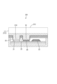
- FIG. 2 is a cross-sectional view of the data relay device.
- FIG. 3 is a perspective view of the circuit board.
- FIG. 4 is a perspective view of the heat dissipation member as viewed from below.
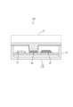
- FIG. 5 is a cross-sectional view of a data relay device according to the second embodiment.
- FIG. 6 is a cross-sectional view of a data relay device according to the third embodiment.
- FIG. 7 is a cross-sectional view of an in-vehicle electronic device according to a comparative example.
- the in-vehicle electronic device comprises a housing, a circuit board housed in the housing, the circuit board having a flash memory and a first electronic component that generates more heat than the flash memory soldered thereto, and a metal heat dissipation member having a heat dissipation portion spaced apart from the circuit board and a first extension portion extending from the heat dissipation portion and in contact with the first electronic component, wherein the flash memory is not in contact with the heat dissipation member.
- In-vehicle electronic device 401 according to the comparative example has a metal heat dissipation member 412.
- Heat dissipation member 412 has a heat dissipation section 417 arranged at a distance from circuit board 411, and an extension section 418 extending from heat dissipation section 417 and in contact with electronic component 430.
- Electronic component 430 is a component that generates more heat than flash memory 432.
- extension section 418 further extends from heat dissipation section 417 toward flash memory 432, and extension section 418 contacts flash memory 432.
- the heat from the electronic component 430 and the heat from the flash memory 432 are averaged by the heat dissipation member 412.
- the heat dissipation member 412. by sharing the temperature burden between the electronic component 430 and the flash memory 432, it is possible to prevent the temperature of the electronic component 430 from rising significantly. In this case, there is an issue that the temperature of the electronic component 430 falls, but the temperature of the flash memory 432 rises.
- the first electronic component contacts the heat dissipation member via the first extension portion, while the flash memory does not contact the heat dissipation member.
- This makes it possible to suppress the temperature rise of the flash memory compared to when the first electronic component and the flash memory are in contact with the heat dissipation member to equalize the temperature.
- This makes it possible to extend the life of the flash memory soldered to the circuit board of the in-vehicle electronic device while suppressing increases in cost and space.
- the flash memory may be covered with a sheet-like insulating material.
- the flash memory is covered with a sheet-like insulating material, so that the temperature of the flash memory can be prevented from increasing due to radiant heat from the first extension portion.
- a sheet-like insulating material may be wrapped around the outer peripheral surface of the first extension portion.
- the temperature of the flash memory may increase due to radiant heat from the first extension.
- the in-vehicle electronic device described in (3) above since the outer peripheral surface of the first extension portion is wrapped with a heat insulating material, it is possible to suppress an increase in temperature of the flash memory due to radiant heat from the first extension portion.
- a sheet-shaped insulating material may be disposed between the heat dissipation section and the circuit board.
- the heat from the heat dissipation section will cause the temperature inside the housing to rise, which may in turn cause the temperature of the flash memory to rise.
- the temperature inside the housing is less likely to rise, which makes it possible to further suppress the temperature rise of the flash memory.
- the first electronic component may be an integrated circuit for arithmetic processing.
- an integrated circuit (IC) for arithmetic processing becomes hot.
- the integrated circuit for arithmetic processing is in contact with the heat dissipation member, whereas the flash memory is not in contact with the heat dissipation member, so that the temperature rise of the flash memory can be suppressed.
- the integrated circuit for arithmetic processing may be an integrated circuit for Ethernet communication that performs arithmetic processing for Ethernet communication.
- integrated circuits used for Ethernet communication become very hot.
- the integrated circuit for Ethernet communication is in contact with the heat dissipation member, whereas the flash memory is not in contact with the heat dissipation member, so that the temperature rise of the flash memory can be suppressed.
- a second electronic component that generates less heat than the first electronic component is soldered to the circuit board, and the heat dissipation member may have a second extension portion extending from the heat dissipation portion and in contact with the second electronic component.
- the second electronic component which generates less heat than the first electronic component, is in contact with the heat dissipation member via the second extension portion, so that the temperature is equalized between the first electronic component and the second electronic component, thereby preventing the temperature of the first electronic component from rising significantly.
- a data relay device 1 as an in-vehicle electronic device according to the first embodiment will be described with reference to Fig. 1.
- the data relay device 1 is a device that relays data between a plurality of in-vehicle networks having different communication protocols.
- the data relay device 1 is called, for example, a CGW-ECU (Central Gateway - Electronic Control Unit).
- Examples of the multiple in-vehicle networks include a Controller Area Network (CAN), a Local Interconnect Network (LIN), an in-vehicle Ethernet, etc. At least an in-vehicle Ethernet is connected to the data relay device 1 according to the first embodiment.
- CAN Controller Area Network
- LIN Local Interconnect Network
- Ethernet At least an in-vehicle Ethernet is connected to the data relay device 1 according to the first embodiment.
- the data relay device 1 is generally box-shaped. As shown in Fig. 2, the data relay device 1 includes a housing 10, a circuit board 11 housed in the housing 10, and a heat dissipation member 12.
- the housing 10 is made of resin and has a box-shaped case portion 13 that is open at the top, and a lid portion 14 that is fixed to the top of the case portion 13.
- the case portion 13 has a bottom wall portion 15 that is rectangular when viewed from above, and a side wall portion 16 that rises in an annular shape from the outer periphery of the bottom wall portion 15.
- circuit board 11 An example of the circuit board 11 will be described with reference to Figures 2 and 3. As shown in Figure 2, the circuit board 11 is housed in the housing 10 in a position parallel to the bottom wall portion 15. As shown in Figure 3, a CPU 30, a RAM (random access memory) 31, and a flash memory 32 are mounted by soldering on the upper surface of the circuit board 11. Other components are also mounted on the circuit board 11, but these are omitted.
- the CPU 30 is an example of a first electronic component that generates more heat than a flash memory, an integrated circuit for arithmetic processing, and an integrated circuit for Ethernet communication.
- the RAM 31 is an example of a second electronic component that generates less heat than the first electronic component.
- the CPU 30 is a CPU for Ethernet communication that performs calculation processing for Ethernet communication.
- in-vehicle Ethernet has a high communication speed, so the CPU 30 for Ethernet communication has a large amount of calculation processing per unit time. Therefore, the CPU 30 for Ethernet communication generally generates more heat than the flash memory 32.
- the RAM 31 is a main storage device for the CPU 30 to execute various programs.
- Flash memory 32 is a rewritable non-volatile semiconductor memory. Various programs and data executed by CPU 30 are stored in flash memory 32. Examples of flash memory 32 include NAND type flash ROM and NOR type flash ROM. NAND type flash ROM also includes eMMC (embedded Multi Media Card).
- eMMC embedded Multi Media Card
- the heat dissipation member 12 will be described with reference to Figure 2.
- the heat dissipation member 12 is fixed to the lid portion 14 of the housing 10 with screws, bolts, etc.
- the heat dissipation member 12 is made of a metal such as aluminum or copper, and has a heat dissipation portion 17 that is spaced apart from the circuit board 11, and a first extension portion 18 that extends from the heat dissipation portion 17.
- the heat dissipation portion 17 has a flat board portion 19 and a plurality of heat dissipation fins 20 that are formed integrally with the board portion 19.
- the multiple heat dissipation fins 20 rise parallel to one another from the upper surface of the board portion 19.
- the first extension 18 is provided at a position overlapping the CPU 30 when viewed from above.
- an opening 21 is formed in the lid 14 of the housing 10 at a position corresponding to the first extension 18.
- the first extension 18 passes through the opening 21 in the lid 14 and is inserted into the inside of the housing 10, with its bottom surface in contact with the top surface of the CPU 30. Therefore, heat from the CPU 30 is transferred to the heat dissipation section 17 via the first extension 18.
- a sheet-like insulating material 22 is wrapped around the outer peripheral surface of the first extension portion 18.
- the insulating material 22 is, for example, flexible aerogel.
- the sheet-like insulating material 22 is not limited to flexible aerogel, and can be selected as appropriate as long as it has insulating properties.
- a sheet-like insulating material 23 is disposed between the heat dissipation section 17 and the circuit board 11.
- the insulating material 23 is attached to the underside of the substrate section 19 of the heat dissipation section 17 (specifically, the portion of the underside of the substrate section 19 where the first extension section 18 is not formed).
- the insulating material 23 may be attached to the upper surface of the lid section 14 instead of the underside of the substrate section 19.
- the insulating material 23 may not be attached to either the underside of the substrate section 19 or the upper surface of the lid section 14, but may simply be sandwiched between the underside of the substrate section 19 and the upper surface of the lid section 14.
- the insulating material 22 wrapped around the first extension section 18 and the insulating material 23 attached to the underside of the substrate section 19 may be of different types.
- the heat dissipation section 17 does not have an extension provided at a position overlapping the flash memory 32 when viewed from above. Therefore, the flash memory 32 is not in contact with the heat dissipation member 12 . 2 and 3, the flash memory 32 is covered from above with a sheet-shaped insulating material 24. When viewed from above, the insulating material 24 has a shape that is slightly larger than the shape of the flash memory 32. The type of the insulating material 24 may also be different from the insulating materials 22 and 23.
- the CPU 30 contacts the heat dissipation member 12 via the first extension portion 18, while the flash memory 32 does not contact the heat dissipation member 12, so that it is possible to suppress an increase in temperature of the flash memory 32 compared to a case where the CPU 30 and the flash memory 32 are brought into contact with the heat dissipation member 12 to equalize the temperature. Therefore, it is possible to extend the life of the flash memory 32 soldered to the circuit board 11 provided in the data relay device 1 while suppressing increases in cost and space.
- the flash memory 32 is covered with the sheet-like insulating material 24, so that the temperature of the flash memory 32 can be prevented from increasing due to radiant heat from the first extension section 18.
- the insulating material 22 is wrapped around the outer peripheral surface of the first extension portion 18, so that the temperature of the flash memory 32 can be prevented from increasing due to radiant heat from the first extension portion 18.
- the sheet-like insulating material 23 is disposed between the heat dissipation section 17 and the circuit board 11, so the temperature inside the housing 10 is less likely to rise. This makes it possible to further suppress the rise in temperature of the flash memory 32.
- the first electronic component that generates more heat than the flash memory 32 is the CPU 30.
- the CPU 30 is in contact with the heat dissipation member 12, whereas the flash memory 32 is not in contact with the heat dissipation member 12, so that the rise in temperature of the flash memory 32 can be suppressed.
- the CPU 30 is a CPU for Ethernet communication. According to the data relay device 1, the CPU 30 for Ethernet communication is in contact with the heat dissipation member 12, while the flash memory 32 is not in contact with the heat dissipation member 12, so that the temperature rise of the flash memory 32 can be suppressed.
- a data relay device 201 according to the second embodiment will be described with reference to Fig. 5.
- the heat dissipation member 212 of the data relay device 201 has a second extension 218 extending from the heat dissipation section 17.
- the lower surface of the second extension 218 is in contact with the RAM 31.
- a sheet-like heat insulating material 22 is also wrapped around the outer peripheral surface of the second extension 218.
- the data relay device 201 according to the second embodiment is substantially the same as the data relay device 1 according to the first embodiment in other respects.
- the RAM 31, which generates less heat than the CPU 30, is in contact with the second extension 218, and the temperature is equalized between the CPU 30 and the RAM 31, thereby preventing the temperature of the CPU 30 from rising significantly.
- the lifespan of the RAM 31 is unlikely to be shortened even if it becomes hot, so even if the temperature of the RAM 31 rises due to the equalization, the lifespan of the RAM 31 is unlikely to be shortened.
- a data relay device 301 according to the third embodiment will be described with reference to Fig. 6.
- the data relay device 301 does not include the cover portion 14 of the first embodiment.
- the data relay device 301 according to the third embodiment is substantially the same as the data relay device 1 according to the first embodiment in other respects.
- the data relay device 1 according to the third embodiment does not have a cover portion 14, so the configuration of the data relay device 1 can be simplified.
- the data relay device 1 (CGW-ECU) is used as an example of an in-vehicle electronic device, but the in-vehicle electronic device is not limited to this.
- the in-vehicle electronic device may be an ECU for engine control, an ECU for gear shift control, or an ECU for brake control.
- the in-vehicle electronic device may be an electronic device other than an ECU.
- the CPU 30 is exemplified as an integrated circuit for arithmetic processing, but the integrated circuit for arithmetic processing may be an FPGA (Field Programmable Gate Array), an ASIC (Application Specific Integrated Circuit), or a microcomputer (so-called microcomputer).
- a microcomputer is an integrated circuit in which a CPU, RAM, flash memory, etc. are integrated into a single chip. Since the flash memory of a microcomputer generally has a small capacity, a large-capacity flash memory is often mounted on the circuit board 11 separately from the microcomputer. In this case, the microcomputer is brought into contact with the heat dissipation member 12, while the flash memory mounted separately from the microcomputer is not brought into contact with the heat dissipation member 12, thereby extending the life of the flash memory mounted separately from the microcomputer.
- the underside of the first extension portion 18 is in direct contact with the CPU 30.
- the underside of the first extension portion 18 may be indirectly in contact with the CPU 30 via a thermal pad, thermally conductive grease, a thermally conductive adhesive (e.g., a thermally conductive two-part adhesive), etc.
- the heat dissipation section 17 has a substrate section 19 and a plurality of heat dissipation fins 20, but the heat dissipation section 17 does not have to have the heat dissipation fins 20.
- the heat dissipation section 17 may be composed of only the substrate section 19.
- the housing 10 is made of resin, but the housing 10 may be made of metal.
- the RAM 31 is exemplified as the second electronic component, but the second electronic component is not limited to the RAM 31 as long as it is an electronic component that generates less heat than the first electronic component.
- the second electronic component may be a power supply IC or a FET (Field Effect Transistor).
- first extension portion 18 and the second extension portion 218 extend straight toward the circuit board 11, but they may extend while bending.
- Data relay device (an example of an in-vehicle electronic device) 10: Housing 11: Circuit board 12: Heat dissipation member 13: Case portion 14: Lid portion 15: Bottom wall portion 16: Side wall portion 17: Heat dissipation portion 18: First extension portion 19: Substrate portion 20: Heat dissipation fins 21: Opening 22: Heat insulating material 23: Heat insulating material 24: Heat insulating material 30: CPU (an example of a first electronic component, an integrated circuit for arithmetic processing, and an integrated circuit for Ethernet communication) 31: RAM (an example of a second electronic component) 32: Flash memory 201: Data relay device 212: Heat dissipation member 218: Second extension portion 301: Data relay device 401: Vehicle-mounted electronic device 411: Circuit board 412: Heat dissipation member 417: Heat dissipation portion 418: Extension portion 430: Electronic component 432: Flash memory
Landscapes
- Physics & Mathematics (AREA)
- Thermal Sciences (AREA)
- Engineering & Computer Science (AREA)
- Microelectronics & Electronic Packaging (AREA)
- Cooling Or The Like Of Electrical Apparatus (AREA)
- Cooling Or The Like Of Semiconductors Or Solid State Devices (AREA)
Abstract
本開示の車載用電子機器は、筐体10と、筐体10に収容されている回路基板11であって、フラッシュメモリ32と、フラッシュメモリ32より発熱量が多い第1の電子部品とが半田付けされている回路基板11と、金属製の放熱部材12であって、回路基板11から離間している放熱部17と、放熱部17から延びており、第1の電子部品に接触している第1の延伸部18と、を有する放熱部材12と、を備え、フラッシュメモリ32が放熱部材12に接触していない。
Description
本明細書で開示する技術は、車載用電子機器に関する。
筐体と、筐体に収容されている回路基板とを備える電子機器は、何らかの熱対策が求められることがある(例えば、特許文献1参照)。特許文献1に記載の電子機器は、天板とシールドケースとの間にスポンジ状部材からなる枠体を配置して風洞を構成し、ファンから導かれたシールドケース内の空気を、天板に開けた放熱孔まで導くようにしている。
電子機器の中には車両に搭載されるものがある。車両に搭載される電子機器(以下、車載用電子機器という)は、回路基板にフラッシュメモリが搭載されていることがある。回路基板にフラッシュメモリを搭載する場合、回路基板に設けたコネクタにフラッシュメモリを差し込むことによって搭載することも可能である。しかしながら、車載用電子機器の場合は車両の振動によってフラッシュメモリがコネクタから外れることが懸念されるため、一般に半田付けによって回路基板に固定されている。
フラッシュメモリは高温になるほど寿命が短くなることが知られている。フラッシュメモリがコネクタに差し込まれている場合はフラッシュメモリが寿命に至っても交換が容易であるが、車載用電子機器の場合はフラッシュメモリが半田付けされているので交換が容易ではない。
このため、車載用電子機器の場合は、フラッシュメモリの交換を不要にするために、フラッシュメモリに熱対策を施して長寿命化することが望まれる。この場合、前述した特許文献1に記載の電子機器のように筐体内にファンを設置することも考えられるが、一般に車載用電子機器はコストやスペースなどの観点でファンが搭載されていないことが多い。車両内には空気の流れが生じ難いので、車両内の空気の流れによってフラッシュメモリを冷却することも難しい。
このため、車載用電子機器の場合は、フラッシュメモリの交換を不要にするために、フラッシュメモリに熱対策を施して長寿命化することが望まれる。この場合、前述した特許文献1に記載の電子機器のように筐体内にファンを設置することも考えられるが、一般に車載用電子機器はコストやスペースなどの観点でファンが搭載されていないことが多い。車両内には空気の流れが生じ難いので、車両内の空気の流れによってフラッシュメモリを冷却することも難しい。
本明細書では、車載用電子機器が備える回路基板に半田付けされているフラッシュメモリを、コストの増加やスペースの増大を抑制しつつ長寿命化する技術を開示する。
本開示に係る車載用電子機器は、車載用電子機器であって、筐体と、前記筐体に収容されている回路基板であって、フラッシュメモリと、前記フラッシュメモリより発熱量が多い第1の電子部品とが半田付けされている回路基板と、金属製の放熱部材であって、前記回路基板から離間している放熱部と、前記放熱部から延びており、前記第1の電子部品に接触している第1の延伸部と、を有する放熱部材と、を備え、前記フラッシュメモリが前記放熱部材に接触していない。
本開示によれば、車載用電子機器が備える回路基板に半田付けされているフラッシュメモリを、コストの増加やスペースの増大を抑制しつつ長寿命化できる。
[本開示の実施形態の説明]
最初に本開示の実施態様を列挙して説明する。
最初に本開示の実施態様を列挙して説明する。
(1)本開示に係る車載用電子機器は、筐体と、前記筐体に収容されている回路基板であって、フラッシュメモリと、前記フラッシュメモリより発熱量が多い第1の電子部品とが半田付けされている回路基板と、金属製の放熱部材であって、前記回路基板から離間している放熱部と、前記放熱部から延びており、前記第1の電子部品に接触している第1の延伸部と、を有する放熱部材と、を備え、前記フラッシュメモリが前記放熱部材に接触していない。
上記(1)に記載の車載用電子機器の効果を、図7に示す比較例を参照しつつ説明する。比較例に係る車載用電子機器401は金属製の放熱部材412を備えている。放熱部材412は回路基板411から離間して配されている放熱部417と、放熱部417から延びており、電子部品430に接触している延伸部418と、を有している。電子部品430はフラッシュメモリ432より発熱量が多い部品である。そして、比較例に係る車載用電子機器401では更に放熱部417からフラッシュメモリ432に向かって延伸部418が延びており、延伸部418がフラッシュメモリ432に接触している。
比較例に係る車載用電子機器401では、電子部品430の熱とフラッシュメモリ432の熱とが放熱部材412によって平準化される。言い換えると、電子部品430とフラッシュメモリ432との間で温度の負担を分担することにより、電子部品430の温度が大きく上昇することを抑制できる。この場合、電子部品430の温度は低下するが、フラッシュメモリ432の温度は上昇するという課題がある。
これに対し、上記(1)に記載の車載用電子機器によると、第1の電子部品は第1の延伸部を介して放熱部材に接触する一方、フラッシュメモリは放熱部材に接触しないので、第1の電子部品とフラッシュメモリとを放熱部材に接触させて温度を平準化する場合に比べ、フラッシュメモリの温度の上昇を抑制できる。このため、車載用電子機器が備える回路基板に半田付けされているフラッシュメモリを、コストの増加やスペースの増大を抑制しつつ長寿命化できる。
(2)上記(1)に記載の車載用電子機器であって、前記フラッシュメモリがシート状の断熱材で覆われていてもよい。
上記(2)に記載の車載用電子機器によると、フラッシュメモリがシート状の断熱材で覆われているので、第1の延伸部からの輻射熱によってフラッシュメモリの温度が上昇することを抑制できる。
(3)上記(1)又は(2)に記載の車載用電子機器であって、前記第1の延伸部の外周面にシート状の断熱材が巻かれていてもよい。
第1の延伸部に断熱材が巻かれていないと第1の延伸部からの輻射熱によってフラッシュメモリの温度が上昇する可能性がある。
上記(3)に記載の車載用電子機器によると、第1の延伸部の外周面に断熱材が巻かれているので、第1の延伸部からの輻射熱によってフラッシュメモリの温度が上昇することを抑制できる。
上記(3)に記載の車載用電子機器によると、第1の延伸部の外周面に断熱材が巻かれているので、第1の延伸部からの輻射熱によってフラッシュメモリの温度が上昇することを抑制できる。
(4)上記(1)又は(2)に記載の車載用電子機器であって、前記放熱部と前記回路基板との間にシート状の断熱材が配されていてもよい。
放熱部と回路基板との間にシート状の断熱材が配されていないと、放熱部の熱によって筐体内の温度が上昇し、それによりフラッシュメモリの温度が上昇する可能性がある。
上記(4)に記載の車載用電子機器によると、放熱部と回路基板との間にシート状の断熱材が配されているので、筐体内の温度が上昇し難くなる。これによりフラッシュメモリの温度の上昇をより抑制できる。
上記(4)に記載の車載用電子機器によると、放熱部と回路基板との間にシート状の断熱材が配されているので、筐体内の温度が上昇し難くなる。これによりフラッシュメモリの温度の上昇をより抑制できる。
(5)上記(1)又は(2)に記載の車載用電子機器であって、前記第1の電子部品は演算処理用の集積回路であってもよい。
一般に演算処理用の集積回路(IC:Integrated Circuit)は高温になる。
上記(5)に記載の車載用電子機器によると、演算処理用の集積回路は放熱部材に接触する一方、フラッシュメモリは放熱部材に接触しないので、フラッシュメモリの温度の上昇を抑制できる。
上記(5)に記載の車載用電子機器によると、演算処理用の集積回路は放熱部材に接触する一方、フラッシュメモリは放熱部材に接触しないので、フラッシュメモリの温度の上昇を抑制できる。
(6)上記(5)に記載の車載用電子機器であって、前記演算処理用の集積回路は、イーサネット(登録商標)通信のための演算処理を行うイーサネット通信用の集積回路であってもよい。
一般にイーサネット通信用の集積回路は高温になる。
上記(6)に記載の車載用電子機器によると、イーサネット通信用の集積回路は放熱部材に接触する一方、フラッシュメモリは放熱部材に接触しないので、フラッシュメモリの温度の上昇を抑制できる。
一般にイーサネット通信用の集積回路は高温になる。
上記(6)に記載の車載用電子機器によると、イーサネット通信用の集積回路は放熱部材に接触する一方、フラッシュメモリは放熱部材に接触しないので、フラッシュメモリの温度の上昇を抑制できる。
(7)上記(1)又は(2)に記載の車載用電子機器であって、前記回路基板に前記第1の電子部品より発熱量が少ない第2の電子部品が半田付けされており、前記放熱部材は、前記放熱部から延びている第2の延伸部であって、前記第2の電子部品に接触している第2の延伸部を有してもよい。
上記(7)に記載の車載用電子機器によると、第1の電子部品より発熱量が少ない第2の電子部品が第2の延伸部を介して放熱部材に接触しているので、第1の電子部品と第2の電子部品との間で温度が平準化されることにより、第1の電子部品の温度が大きく上昇することを抑制できる。
[本開示の実施形態の詳細]
以下に、本開示の実施形態について説明する。本開示はこれらの例示に限定されるものではなく、特許請求の範囲によって示され、特許請求の範囲と均等の意味および範囲内での全ての変更が含まれることが意図される。
[本開示の実施形態の詳細]
以下に、本開示の実施形態について説明する。本開示はこれらの例示に限定されるものではなく、特許請求の範囲によって示され、特許請求の範囲と均等の意味および範囲内での全ての変更が含まれることが意図される。
<実施形態1>
実施形態1を図1ないし図4によって説明する。以降の説明において上下方向、前後方向及び左右方向とは図1に示す上下方向、前後方向及び左右方向を基準とする。
実施形態1を図1ないし図4によって説明する。以降の説明において上下方向、前後方向及び左右方向とは図1に示す上下方向、前後方向及び左右方向を基準とする。
図1を参照して、実施形態1に係る車載用電子機器としてのデータ中継装置1について説明する。データ中継装置1は通信プロトコルが異なる複数の車載ネットワーク間でデータを中継する装置である。データ中継装置1は例えばCGW-ECU(Central Gateway - Electronic Control Unit)と称されている。
複数の車載ネットワークとしてはCAN(Controller Area Network)、LIN(Local Interconnect Network)、車載イーサネットなどが例示される。実施形態1に係るデータ中継装置1には少なくとも車載イーサネットが接続される。
複数の車載ネットワークとしてはCAN(Controller Area Network)、LIN(Local Interconnect Network)、車載イーサネットなどが例示される。実施形態1に係るデータ中継装置1には少なくとも車載イーサネットが接続される。
図1に示すように、データ中継装置1は概ね箱状である。図2に示すように、データ中継装置1は筐体10と、筐体10に収容されている回路基板11と、放熱部材12とを備えている。
筐体10は樹脂製であり、上側が開口している箱状のケース部13と、ケース部13の上側に固定されている蓋部14とを有している。ケース部13は上側から見て矩形状の底壁部15と、底壁部15の外周縁部から環状に立ち上がっている側壁部16とを有している。
筐体10は樹脂製であり、上側が開口している箱状のケース部13と、ケース部13の上側に固定されている蓋部14とを有している。ケース部13は上側から見て矩形状の底壁部15と、底壁部15の外周縁部から環状に立ち上がっている側壁部16とを有している。
図2及び図3を参照して、回路基板11の一例について説明する。図2に示すように、回路基板11は底壁部15と平行な姿勢で筐体10に収容されている。図3に示すように、回路基板11の上面にはCPU30、RAM(ランダムアクセスメモリ)31、及び、フラッシュメモリ32が半田付けによって搭載されている。回路基板11には他の部品も搭載されているが、他の部品は省略している。
CPU30はフラッシュメモリより発熱量が多い第1の電子部品、演算処理用の集積回路、及び、イーサネット通信用の集積回路の一例である。RAM31は第1の電子部品より発熱量が少ない第2の電子部品の一例である。
CPU30はフラッシュメモリより発熱量が多い第1の電子部品、演算処理用の集積回路、及び、イーサネット通信用の集積回路の一例である。RAM31は第1の電子部品より発熱量が少ない第2の電子部品の一例である。
CPU30はイーサネット通信のための演算処理を行うイーサネット通信用のCPUである。一般に車載イーサネットは通信速度が速いため、イーサネット通信用のCPU30は単位時間当たりの演算処理量が多い。このため、一般にイーサネット通信用のCPU30はフラッシュメモリ32より発熱量が多い。
RAM31はCPU30が各種のプログラムを実行するための主記憶装置である。
RAM31はCPU30が各種のプログラムを実行するための主記憶装置である。
フラッシュメモリ32は書き換え可能な不揮発性の半導体メモリである。フラッシュメモリ32にはCPU30によって実行される各種のプログラムやデータが記憶されている。フラッシュメモリ32としてはNAND型のフラッシュROM、NOR型のフラッシュROMなどが例示される。NAND型のフラッシュROMにはeMMC(embedded Multi Media Card)も含まれる。
図2を参照して、放熱部材12について説明する。放熱部材12は筐体10の蓋部14にネジやボルトなどで固定されている。放熱部材12はアルミや銅などの金属製であり、回路基板11から離間している放熱部17と、放熱部17から延びている第1の延伸部18とを有している。放熱部17は平板状の基板部19と、基板部19に一体に形成されている複数の放熱フィン20とを有している。複数の放熱フィン20は基板部19の上面から互いに平行に立ち上がっている。
図2及び図4に示すように、第1の延伸部18は上側から見てCPU30と重なる位置に設けられている。図2に示すように、筐体10の蓋部14には第1の延伸部18に対応する位置に開口21が形成されている。第1の延伸部18は蓋部14の開口21を通過して筐体10の内部に挿入されており、下面がCPU30の上面に接触している。このためCPU30の熱が第1の延伸部18を介して放熱部17に伝達される。
第1の延伸部18の外周面にはシート状の断熱材22が巻かれている。断熱材22は例えばフレキシブルエアロゲルである。シート状の断熱材22は断熱性を有するものであればフレキシブルエアロゲルに限定されず、適宜に選択可能である。
放熱部17と回路基板11との間にはシート状の断熱材23が配されている。断熱材23は放熱部17の基板部19の下面(具体的には基板部19の下面のうち第1の延伸部18が形成されていない部分)に貼り付けられている。断熱材23は基板部19の下面ではなく蓋部14の上面に貼り付けられていてもよい。あるいは、断熱材23は基板部19の下面及び蓋部14の上面のどちらにも貼り付けられておらず、基板部19の下面と蓋部14の上面とに挟持されているだけでもよい。第1の延伸部18に巻かれている断熱材22と基板部19の下面に貼り付けられている断熱材23とは種類が異なってもよい。
放熱部17は、上側から見てフラッシュメモリ32と重なる位置に延伸部が設けられていない。このためフラッシュメモリ32は放熱部材12に接触していない。
図2及び図3に示すように、フラッシュメモリ32はシート状の断熱材24で上から覆われている。断熱材24は上側から見てフラッシュメモリ32の形状よりも一回り大きい形状である。断熱材24の種類も断熱材22や断熱材23と異なっていてもよい。
図2及び図3に示すように、フラッシュメモリ32はシート状の断熱材24で上から覆われている。断熱材24は上側から見てフラッシュメモリ32の形状よりも一回り大きい形状である。断熱材24の種類も断熱材22や断熱材23と異なっていてもよい。
(2)実施形態の効果
実施形態1に係るデータ中継装置1によると、CPU30は第1の延伸部18を介して放熱部材12に接触する一方、フラッシュメモリ32は放熱部材12に接触しないので、CPU30とフラッシュメモリ32とを放熱部材12に接触させて温度を平準化する場合に比べ、フラッシュメモリ32の温度の上昇を抑制できる。このため、データ中継装置1が備える回路基板11に半田付けされているフラッシュメモリ32を、コストの増加やスペースの増大を抑制しつつ長寿命化できる。
実施形態1に係るデータ中継装置1によると、CPU30は第1の延伸部18を介して放熱部材12に接触する一方、フラッシュメモリ32は放熱部材12に接触しないので、CPU30とフラッシュメモリ32とを放熱部材12に接触させて温度を平準化する場合に比べ、フラッシュメモリ32の温度の上昇を抑制できる。このため、データ中継装置1が備える回路基板11に半田付けされているフラッシュメモリ32を、コストの増加やスペースの増大を抑制しつつ長寿命化できる。
データ中継装置1によると、フラッシュメモリ32がシート状の断熱材24で覆われているので、第1の延伸部18からの輻射熱によってフラッシュメモリ32の温度が上昇することを抑制できる。
データ中継装置1によると、第1の延伸部18の外周面に断熱材22が巻かれているので、第1の延伸部18からの輻射熱によってフラッシュメモリ32の温度が上昇することを抑制できる。
データ中継装置1によると、放熱部17と回路基板11との間にシート状の断熱材23が配されているので、筐体10内の温度が上昇し難くなる。これによりフラッシュメモリ32の温度の上昇をより抑制できる。
データ中継装置1によると、フラッシュメモリ32より発熱量が多い第1の電子部品はCPU30である。データ中継装置1によると、CPU30は放熱部材12に接触する一方、フラッシュメモリ32は放熱部材12に接触しないので、フラッシュメモリ32の温度の上昇を抑制できる。
データ中継装置1によると、CPU30はイーサネット通信用のCPUである。データ中継装置1によると、イーサネット通信用のCPU30は放熱部材12に接触する一方、フラッシュメモリ32は放熱部材12に接触しないので、フラッシュメモリ32の温度の上昇を抑制できる。
<実施形態2>
図5を参照して、実施形態2に係るデータ中継装置201について説明する。データ中継装置201の放熱部材212は、放熱部17から延びている第2の延伸部218を有している。第2の延伸部218の下面はRAM31に接触している。第2の延伸部218の外周面にもシート状の断熱材22が巻かれている。
実施形態2に係るデータ中継装置201はその他の点において実施形態1に係るデータ中継装置1と実質的に同一である。
図5を参照して、実施形態2に係るデータ中継装置201について説明する。データ中継装置201の放熱部材212は、放熱部17から延びている第2の延伸部218を有している。第2の延伸部218の下面はRAM31に接触している。第2の延伸部218の外周面にもシート状の断熱材22が巻かれている。
実施形態2に係るデータ中継装置201はその他の点において実施形態1に係るデータ中継装置1と実質的に同一である。
実施形態2に係るデータ中継装置201によると、CPU30より発熱量が少ないRAM31が第2の延伸部218に接触しているので、CPU30とRAM31との間で温度が平準化されることにより、CPU30の温度が大きく上昇することを抑制できる。一般にRAM31は高温になっても寿命が短くなり難いので、平準化によってRAM31の温度が上昇してもRAM31の寿命は短くなり難い。
<実施形態3>
図6を参照して、実施形態3に係るデータ中継装置301について説明する。データ中継装置301は実施形態1の蓋部14を備えていない。実施形態3に係るデータ中継装置301はその他の点において実施形態1に係るデータ中継装置1と実質的に同一である。
図6を参照して、実施形態3に係るデータ中継装置301について説明する。データ中継装置301は実施形態1の蓋部14を備えていない。実施形態3に係るデータ中継装置301はその他の点において実施形態1に係るデータ中継装置1と実質的に同一である。
実施形態3に係るデータ中継装置1によると、蓋部14を備えていないのでデータ中継装置1の構成を簡素にできる。
<他の実施形態>
本明細書によって開示される技術は上記記述及び図面によって説明した実施形態に限定されるものではなく、例えば次のような実施形態も本明細書によって開示される技術的範囲に含まれる。
本明細書によって開示される技術は上記記述及び図面によって説明した実施形態に限定されるものではなく、例えば次のような実施形態も本明細書によって開示される技術的範囲に含まれる。
(1)上記実施形態では車載用電子機器としてデータ中継装置1(CGW-ECU)を例示したが、車載用電子機器はこれに限定されない。例えば、車載用電子機器はエンジン制御用のECUでもよいし、変速制御用のECUでもよいし、ブレーキ制御用のECUでもよい。車載用電子機器はECU以外の電子機器であってもよい。
(2)上記実施形態では演算処理用の集積回路としてCPU30を例示したが、演算処理用の集積回路はFPGA(Field Programmable Gate Array)でもよいし、ASIC(Application Specific Integrated Circuit)でもよいし、マイクロコンピュータ(所謂マイコン)でもよい。マイコンはCPU、RAM、フラッシュメモリなどが1チップ化された集積回路である。一般にマイコンのフラッシュメモリは小容量であるので、マイコンとは別に大容量のフラッシュメモリが回路基板11に搭載されることが多い。その場合はマイコンを放熱部材12に接触させる一方、マイコンとは別に搭載されているフラッシュメモリは放熱部材12に接触させないことにより、マイコンとは別に搭載されているフラッシュメモリを長寿命化できる。
(3)上記実施形態では第1の延伸部18の下面がCPU30に直に接触している場合を例示した。これに対し、第1の延伸部18の下面はサーマルパッド、熱伝導グリス、熱伝導性を有する接着剤(例えば熱伝導性を有する二液接着剤)などを介して間接的にCPU30に接触してもよい。
(4)上記実施形態では放熱部17が基板部19と複数の放熱フィン20とを有している場合を例示したが、放熱部17は放熱フィン20を有していなくてもよい。すなわち放熱部17は基板部19だけで構成されてもよい。
(5)上記実施形態では筐体10が樹脂製である場合を例示したが、筐体10は金属製であってもよい。
(6)上記実施形態では第2の電子部品としてRAM31を例示したが、第2の電子部品は第1の電子部品より発熱量が少ない電子部品であればRAM31に限定されない。例えば、第2の電子部品は電源ICでもよいし、FET(Field Effect Transistor)でもよい。
(7)上記実施形態では第1の延伸部18や第2の延伸部218が回路基板11に向かって真っ直ぐ伸びている場合を例示したが、これらは曲がりながら延びていてもよい。
1: データ中継装置(車載用電子機器の一例)
10: 筐体
11: 回路基板
12: 放熱部材
13: ケース部
14: 蓋部
15: 底壁部
16: 側壁部
17: 放熱部
18: 第1の延伸部
19: 基板部
20: 放熱フィン
21: 開口
22: 断熱材
23: 断熱材
24: 断熱材
30: CPU(第1の電子部品、演算処理用の集積回路、及び、イーサネット通信用の集積回路の一例)
31: RAM(第2の電子部品の一例)
32: フラッシュメモリ
201: データ中継装置
212: 放熱部材
218: 第2の延伸部
301: データ中継装置
401: 車載用電子機器
411: 回路基板
412: 放熱部材
417: 放熱部
418: 延伸部
430: 電子部品
432: フラッシュメモリ
10: 筐体
11: 回路基板
12: 放熱部材
13: ケース部
14: 蓋部
15: 底壁部
16: 側壁部
17: 放熱部
18: 第1の延伸部
19: 基板部
20: 放熱フィン
21: 開口
22: 断熱材
23: 断熱材
24: 断熱材
30: CPU(第1の電子部品、演算処理用の集積回路、及び、イーサネット通信用の集積回路の一例)
31: RAM(第2の電子部品の一例)
32: フラッシュメモリ
201: データ中継装置
212: 放熱部材
218: 第2の延伸部
301: データ中継装置
401: 車載用電子機器
411: 回路基板
412: 放熱部材
417: 放熱部
418: 延伸部
430: 電子部品
432: フラッシュメモリ
Claims (7)
- 車載用電子機器であって、
筐体と、
前記筐体に収容されている回路基板であって、フラッシュメモリと、前記フラッシュメモリより発熱量が多い第1の電子部品とが半田付けされている回路基板と、
金属製の放熱部材であって、前記回路基板から離間している放熱部と、前記放熱部から延びており、前記第1の電子部品に接触している第1の延伸部と、を有する放熱部材と、
を備え、
前記フラッシュメモリが前記放熱部材に接触していない、車載用電子機器。 - 請求項1に記載の車載用電子機器であって、
前記フラッシュメモリがシート状の断熱材で覆われている、車載用電子機器。 - 請求項1又は請求項2に記載の車載用電子機器であって、
前記第1の延伸部の外周面にシート状の断熱材が巻かれている、車載用電子機器。 - 請求項1又は請求項2に記載の車載用電子機器であって、
前記放熱部と前記回路基板との間にシート状の断熱材が配されている、車載用電子機器。 - 請求項1又は請求項2に記載の車載用電子機器であって、
前記第1の電子部品は演算処理用の集積回路である、車載用電子機器。 - 請求項5に記載の車載用電子機器であって、
前記演算処理用の集積回路は、イーサネット通信のための演算処理を行うイーサネット通信用の集積回路である、車載用電子機器。 - 請求項1又は請求項2に記載の車載用電子機器であって、
前記回路基板に前記第1の電子部品より発熱量が少ない第2の電子部品が半田付けされており、
前記放熱部材は、前記放熱部から延びている第2の延伸部であって、前記第2の電子部品に接触している第2の延伸部を有する、車載用電子機器。
Applications Claiming Priority (2)
| Application Number | Priority Date | Filing Date | Title |
|---|---|---|---|
| JP2023094597A JP2024176215A (ja) | 2023-06-08 | 2023-06-08 | 車載用電子機器 |
| JP2023-094597 | 2023-06-08 |
Publications (1)
| Publication Number | Publication Date |
|---|---|
| WO2024252942A1 true WO2024252942A1 (ja) | 2024-12-12 |
Family
ID=93795871
Family Applications (1)
| Application Number | Title | Priority Date | Filing Date |
|---|---|---|---|
| PCT/JP2024/019005 Ceased WO2024252942A1 (ja) | 2023-06-08 | 2024-05-23 | 車載用電子機器 |
Country Status (2)
| Country | Link |
|---|---|
| JP (1) | JP2024176215A (ja) |
| WO (1) | WO2024252942A1 (ja) |
Citations (6)
| Publication number | Priority date | Publication date | Assignee | Title |
|---|---|---|---|---|
| JP2005150249A (ja) * | 2003-11-12 | 2005-06-09 | Otsuka Denki Kk | 熱伝導部材とそれを用いた放熱用構造体 |
| JP2006269685A (ja) * | 2005-03-23 | 2006-10-05 | Fujitsu Ltd | 受熱シート、電子機器及び受熱シートの製造方法 |
| JP2013254791A (ja) * | 2012-06-05 | 2013-12-19 | Nec Corp | 放熱機構およびその放熱機構を備えた電子機器 |
| US20140022733A1 (en) * | 2012-07-19 | 2014-01-23 | Samsung Electronics Co., Ltd. | Storage Device |
| JP2019075507A (ja) * | 2017-10-18 | 2019-05-16 | 日本碍子株式会社 | 放熱部材、放熱構造及び電子機器 |
| JP2022070415A (ja) * | 2020-10-27 | 2022-05-13 | 日立Astemo株式会社 | 電子制御装置 |
-
2023
- 2023-06-08 JP JP2023094597A patent/JP2024176215A/ja active Pending
-
2024
- 2024-05-23 WO PCT/JP2024/019005 patent/WO2024252942A1/ja not_active Ceased
Patent Citations (6)
| Publication number | Priority date | Publication date | Assignee | Title |
|---|---|---|---|---|
| JP2005150249A (ja) * | 2003-11-12 | 2005-06-09 | Otsuka Denki Kk | 熱伝導部材とそれを用いた放熱用構造体 |
| JP2006269685A (ja) * | 2005-03-23 | 2006-10-05 | Fujitsu Ltd | 受熱シート、電子機器及び受熱シートの製造方法 |
| JP2013254791A (ja) * | 2012-06-05 | 2013-12-19 | Nec Corp | 放熱機構およびその放熱機構を備えた電子機器 |
| US20140022733A1 (en) * | 2012-07-19 | 2014-01-23 | Samsung Electronics Co., Ltd. | Storage Device |
| JP2019075507A (ja) * | 2017-10-18 | 2019-05-16 | 日本碍子株式会社 | 放熱部材、放熱構造及び電子機器 |
| JP2022070415A (ja) * | 2020-10-27 | 2022-05-13 | 日立Astemo株式会社 | 電子制御装置 |
Also Published As
| Publication number | Publication date |
|---|---|
| JP2024176215A (ja) | 2024-12-19 |
Similar Documents
| Publication | Publication Date | Title |
|---|---|---|
| JP4877389B2 (ja) | 自動変速機用コントロールユニット冷却装置 | |
| JP2006303106A (ja) | 電子回路装置 | |
| JP7234044B2 (ja) | ステレオカメラ | |
| JP4023054B2 (ja) | 電子回路ユニット | |
| JP7618399B2 (ja) | 電子機器の温度調整構造 | |
| CN110383612B (zh) | 电气连接箱 | |
| CN105493648B (zh) | 车辆用电子控制装置 | |
| JP4387314B2 (ja) | 電気接続箱 | |
| WO2022110741A1 (zh) | 具有浮动支撑结构的电子设备 | |
| JP6982776B2 (ja) | 発熱電子部品の放熱装置、車載充電器、および車両 | |
| CN211128747U (zh) | 排热结构及电子设备 | |
| WO2024252942A1 (ja) | 車載用電子機器 | |
| CN104080312A (zh) | 车辆用电子控制装置 | |
| US11848251B2 (en) | Semiconductor device | |
| JP6424839B2 (ja) | 電子制御ユニット、および、これを用いた電動パワーステアリング装置 | |
| JP4851154B2 (ja) | 回路基板内蔵筐体 | |
| KR20200025215A (ko) | 전자제어 장치 | |
| KR101063172B1 (ko) | 전자제어장치 | |
| JP2003188563A (ja) | 電子制御装置 | |
| JP2007216823A (ja) | 車載制御装置のケース収容構造 | |
| JP2021190495A (ja) | 電子制御装置 | |
| JP7746804B2 (ja) | 演算ユニットの冷却構造 | |
| JP7619156B2 (ja) | 電子制御装置 | |
| WO2025215971A1 (ja) | 電気接続ユニット | |
| WO2025135118A1 (ja) | 電子機器の筐体構造 |
Legal Events
| Date | Code | Title | Description |
|---|---|---|---|
| 121 | Ep: the epo has been informed by wipo that ep was designated in this application |
Ref document number: 24819174 Country of ref document: EP Kind code of ref document: A1 |
|
| NENP | Non-entry into the national phase |
Ref country code: DE |