WO2024252915A1 - 電子部品及びこれを備える回路モジュール - Google Patents
電子部品及びこれを備える回路モジュール Download PDFInfo
- Publication number
- WO2024252915A1 WO2024252915A1 PCT/JP2024/018609 JP2024018609W WO2024252915A1 WO 2024252915 A1 WO2024252915 A1 WO 2024252915A1 JP 2024018609 W JP2024018609 W JP 2024018609W WO 2024252915 A1 WO2024252915 A1 WO 2024252915A1
- Authority
- WO
- WIPO (PCT)
- Prior art keywords
- conductor pattern
- conductor
- coil
- electrically connected
- terminal electrode
- Prior art date
- Legal status (The legal status is an assumption and is not a legal conclusion. Google has not performed a legal analysis and makes no representation as to the accuracy of the status listed.)
- Ceased
Links
Images



Classifications
-
- H—ELECTRICITY
- H01—ELECTRIC ELEMENTS
- H01F—MAGNETS; INDUCTANCES; TRANSFORMERS; SELECTION OF MATERIALS FOR THEIR MAGNETIC PROPERTIES
- H01F17/00—Fixed inductances of the signal type
-
- H—ELECTRICITY
- H01—ELECTRIC ELEMENTS
- H01F—MAGNETS; INDUCTANCES; TRANSFORMERS; SELECTION OF MATERIALS FOR THEIR MAGNETIC PROPERTIES
- H01F17/00—Fixed inductances of the signal type
- H01F17/04—Fixed inductances of the signal type with magnetic core
-
- H—ELECTRICITY
- H01—ELECTRIC ELEMENTS
- H01F—MAGNETS; INDUCTANCES; TRANSFORMERS; SELECTION OF MATERIALS FOR THEIR MAGNETIC PROPERTIES
- H01F27/00—Details of transformers or inductances, in general
-
- H—ELECTRICITY
- H01—ELECTRIC ELEMENTS
- H01F—MAGNETS; INDUCTANCES; TRANSFORMERS; SELECTION OF MATERIALS FOR THEIR MAGNETIC PROPERTIES
- H01F27/00—Details of transformers or inductances, in general
- H01F27/28—Coils; Windings; Conductive connections
-
- H—ELECTRICITY
- H01—ELECTRIC ELEMENTS
- H01F—MAGNETS; INDUCTANCES; TRANSFORMERS; SELECTION OF MATERIALS FOR THEIR MAGNETIC PROPERTIES
- H01F27/00—Details of transformers or inductances, in general
- H01F27/28—Coils; Windings; Conductive connections
- H01F27/29—Terminals; Tapping arrangements for signal inductances
Definitions
- This disclosure relates to electronic components and circuit modules that include the same.
- Patent documents 1 and 2 disclose coil components with a coil array built into the base body.
- the coil axis of each coil is perpendicular to the mounting surface.
- the coil axis of each coil is horizontal to the mounting surface.
- the coil component of Patent Document 1 has a problem in that the mounting area is large because the coil axis of each coil is perpendicular to the mounting surface.
- the coil component of Patent Document 2 has a problem in that the coil axis of each coil is horizontal to the mounting surface, so the number of layers required increases in proportion to the number of built-in coils.
- This disclosure describes an improved electronic component that includes multiple coils and a circuit module that includes the same.
- An electronic component comprises an element body having first and second surfaces extending in a first direction and a second direction perpendicular to the first direction and differing in position from each other in a third direction perpendicular to the first and second directions, first and second terminal electrodes formed on the first surface and arranged in the first direction, third and fourth terminal electrodes formed on the first surface and arranged in the first direction, a first coil having one end electrically connected to the first terminal electrode and the other end electrically connected to the second terminal electrode, and a second coil having one end electrically connected to the third terminal electrode and the other end electrically connected to the fourth terminal electrode, the first coil being formed in the first direction on the first surface and including a first conductor pattern having one end located on the first terminal electrode side and the other end located on the second terminal electrode side, and a second conductor pattern formed on the second surface and having one end electrically connected to the first terminal electrode and the other end electrically connected to the other of the first conductor pattern.
- the second coil includes a second conductor pattern electrically connected to one end of the first conductor pattern, and a third conductor pattern formed on the second surface, one end of which is electrically connected to the second terminal electrode and the other end of which is electrically connected to one end of the first conductor pattern.
- the second coil includes a fourth conductor pattern formed on the first surface in a first direction, one end of which is located on the third terminal electrode side and the other end of which is located on the fourth terminal electrode side, a fifth conductor pattern formed on the second surface, one end of which is electrically connected to the third terminal electrode and the other end of which is electrically connected to the other end of the fourth conductor pattern, and a sixth conductor pattern formed on the second surface, one end of which is electrically connected to the fourth terminal electrode and the other end of which is electrically connected to one end of the fourth conductor pattern.
- the first coil and the second coil are disposed adjacent to each other in the second direction, and the first conductor pattern and the fourth conductor pattern are formed at different positions from each other in the first direction.
- a circuit module includes a substrate having first to fourth land patterns and the above-mentioned electronic component mounted on the substrate, and the first to fourth terminal electrodes are connected to the first to fourth land patterns, respectively.
- the present disclosure provides an improved electronic component including multiple coils and a circuit module including the same.
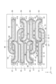
- FIG. 1 is a schematic perspective view showing the appearance of a coil component 100 according to an embodiment of the technology disclosed herein.
- FIG. 2 is a schematic perspective top view of the coil device 100.
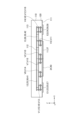
- FIG. 3 is a schematic perspective side view of the coil device 100.
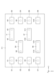
- FIG. 4 is a schematic bottom view of the coil device 100.
- FIG. 5 is a schematic exploded perspective view of a circuit module 200 including the coil component 100.
- FIG. 6 is a schematic perspective top view of a coil component according to a modified example.
- FIG. 7 is a schematic perspective side view of a coil component according to a modified example.
- FIG. 8 is a schematic bottom view of a coil component according to a modified example.
- FIG. 1 is a schematic perspective view showing the appearance of an electronic component (coil component) 100 according to one embodiment of the technology disclosed herein.
- FIG. 2 is a schematic perspective top view of the coil component 100
- FIG. 3 is a schematic perspective side view of the coil component 100
- FIG. 4 is a schematic bottom view of the coil component 100.
- the coil component 100 includes a base body 110, four coils C1 to C4 embedded in the base body 110, and terminal electrodes E1 to E8 exposed on the surface of the base body 110.
- the base body 110 may be made of a composite magnetic material in which magnetic particles made of a high magnetic permeability material such as ferrite or permalloy are bound by a resin binder.
- the base body 110 forms an XY plane and has outer surfaces 111, 113 and an inner layer surface 112 that are located at different positions in the Z direction.
- the outer surface 111 forms the mounting surface of the coil component 100.
- Eight terminal electrodes E1 to E8 are provided on the outer surface 111.
- the outer surface 111 may be covered with a protective film 120 made of resin or the like.
- the outer surface 113 is the upper surface located opposite the outer surface 111.
- the inner surface 112 is a surface located inside the element body 110 and is not exposed to the outside.
- the direction from terminal electrode E1 toward terminal electrode E2 may be referred to as the X direction (or +X direction), and the opposite direction may be referred to as the -X direction.
- the direction from terminal electrode E1 toward terminal electrode E7 may be referred to as the Y direction (or +Y direction), and the opposite direction may be referred to as the -Y direction.
- the direction from outer surface 111 toward outer surface 113 may be referred to as the Z direction (or +Z direction), and the opposite direction may be referred to as the -Z direction.
- the X direction, Y direction, and Z direction are each perpendicular to each other. Note that this disclosure also includes cases where the angles formed by the X direction, Y direction, and Z direction differ from a right angle due to manufacturing errors of coil component 100 (for example, when there is a difference of about 5° from a right angle).
- terminal electrodes E1 to E8 not only the terminal electrodes E1 to E8 but also the conductor patterns 11, 24, 37, and 40 are exposed on the outer surface 111.
- the terminal electrodes E1 to E8 and the conductor patterns 11, 24, 37, and 40 are located on the same conductor layer, but the conductor patterns 11, 24, 37, and 40 are not external terminals, so they may be covered with an insulating film such as resin.
- the terminal electrodes E1 and E2 are arranged in the X direction, and the conductor pattern 11 extending in the X direction is located between them.
- the terminal electrodes E3 and E4 are arranged in the X direction, and the conductor pattern 24 extending in the X direction is located between them.
- the terminal electrodes E5 and E6 are arranged in the X direction, and the conductor pattern 37 extending in the X direction is located between them.
- the terminal electrodes E7 and E8 are arranged in the X direction, and the conductor pattern 40 extending in the X direction is located between them.
- terminal electrodes E1, E3, E5, and E7 are arranged in the Y direction, and terminal electrodes E2, E4, E6, and E8 are arranged in the Y direction. This allows the size of element body 110 in the X direction to be reduced.
- the positions of conductor patterns 11 and 37 in the X direction may be the same, and the positions of conductor patterns 24 and conductor patterns 40 in the X direction may be the same. In contrast, the positions of conductor patterns 11 and 37 in the X direction are different from the positions of conductor patterns 24 and 40 in the X direction. In the example shown in FIG. 4, the positions of conductor patterns 11 and 37 in the X direction do not overlap with the positions of conductor patterns 24 and 40 in the X direction.
- the edge positions of conductor patterns 11 and 37 in the -X direction (the side on which terminal electrodes E1, E3, E5, and E7 are formed in FIG.
- the coil C1 is connected between the terminal electrodes E1 and E2. One end of the coil C1 is electrically connected to the terminal electrode E1, and the other end of the coil C1 is electrically connected to the terminal electrode E2.
- the coil C1 has a conductor pattern 11 located on the outer surface 111, conductor patterns 12 and 13 located on the inner surface 112, and via conductors V1 to V4 that penetrate between the outer surface 111 and the inner surface 112.
- the via conductors V1 to V4 may be arranged in this order in the X direction.
- the conductor pattern 11 extends linearly in the X direction, while the conductor patterns 12 and 13 extend in the X direction while meandering in the Y direction.
- the conductor pattern 12 in a plan view seen from the Z direction, has a first straight portion 51 that is formed linearly in the X direction and has an end in the -X direction connected to the via conductor V1.
- the conductor pattern 12 further has a second straight portion 52 that extends linearly in the X direction and has an end in the -X direction connected to an end in the +X direction of the first straight portion 51 via a first bend 61 and an end in the +X direction connected to the via conductor V3 via a second bend 62.
- the conductor pattern 13 also has a third straight portion 53 that extends linearly in the X direction, with the end in the -X direction connected to the via conductor V2 via the third bend 63, and the end in the +X direction connected to the via conductor V4 via the fourth bend 64.
- one end of conductor pattern 12 in the -X direction is connected to terminal electrode E1 via via conductor V1.
- One end of conductor pattern 13 in the +X direction is connected to terminal electrode E2 via via conductor V4.
- One end of conductor pattern 11 located on the terminal electrode E1 side (-X direction side) is connected to the other end of conductor pattern 13 via via conductor V2.
- the other end of conductor pattern 11 located on the terminal electrode E2 side (+X direction side) is connected to the other end of conductor pattern 12 via via conductor V3.
- a current input from the outside to the terminal electrode E1 flows to the terminal electrode E2 via the via conductor V1, the conductor pattern 12, the via conductor V3, the conductor pattern 11, the via conductor V2, the conductor pattern 13, and the via conductor V4.
- the current mainly flows in the +X direction in the conductor patterns 12 and 13, while the current flows in the -X direction in the conductor pattern 11.
- the current flows in the -Z direction in the via conductor V3, while the current flows in the +Z direction in the via conductor V2.
- the conductor pattern 12, the via conductor V3, the conductor pattern 11, the via conductor V2, and the conductor pattern 13 form a loop with the Y direction as the axial direction.
- a part of the element body 110 is embedded in the area surrounded by the above loop when viewed from the Y direction.
- the part surrounded by this loop becomes the area (the core of the inductor) where a magnetic flux is generated when a current flows through the coil C1.
- the area surrounded by the conductor patterns 12 and 13 overlaps with a part of the conductor pattern 11.
- Coil C2 is disposed adjacent to coils C1 and C3 so as to be sandwiched between them in the Y direction, and is connected between terminal electrodes E3 and E4. One end of coil C2 is electrically connected to terminal electrode E3, and the other end of coil C2 is electrically connected to terminal electrode E4.
- Coil C2 has conductor pattern 24 located on outer surface 111, conductor patterns 25 and 26 located on inner surface 112, and via conductors V5 to V8 that penetrate between outer surface 111 and inner surface 112. Via conductors V5 to V8 may be arranged in this order in the X direction.
- Conductor pattern 24 extends linearly in the X direction, while conductor patterns 25 and 26 extend in the X direction while meandering in the Y direction.
- the conductor pattern 26 in a plan view seen from the Z direction, is formed linearly in the X direction and has a fourth straight portion 54 whose end in the +X direction is connected to the via conductor V8.
- the conductor pattern 26 further has a fifth straight portion 55 which extends linearly in the X direction and whose end in the +X direction is connected to the end in the -X direction of the fourth straight portion 54 via a fifth bend 65 and whose end in the -X direction is connected to the via conductor V6 via a sixth bend 66.
- the conductor pattern 25 also has a sixth straight portion 56 that extends linearly in the X direction, with the end in the +X direction connected to the via conductor V7 via a seventh bend 67, and the end in the -X direction connected to the via conductor V5 via an eighth bend 68.
- one end of conductor pattern 25 in the -X direction is connected to terminal electrode E3 via via conductor V5.
- One end of conductor pattern 26 in the +X direction is connected to terminal electrode E4 via via conductor V8.
- One end of conductor pattern 24 located on the terminal electrode E3 side (-X direction side) is connected to the other end of conductor pattern 26 via via conductor V6.
- the other end of conductor pattern 24 located on the terminal electrode E4 side (+X direction side) is connected to the other end of conductor pattern 25 via via conductor V7.
- a current input from the outside to the terminal electrode E3 flows to the terminal electrode E4 via the via conductor V5, the conductor pattern 25, the via conductor V7, the conductor pattern 24, the via conductor V6, the conductor pattern 26, and the via conductor V8.
- a current mainly flows in the +X direction in the conductor patterns 25 and 26, while a current flows in the -X direction in the conductor pattern 24.
- a current flows in the -Z direction in the via conductor V7, while a current flows in the +Z direction in the via conductor V6.
- the conductor pattern 25, the via conductor V7, the conductor pattern 24, the via conductor V6, and the conductor pattern 26 form a loop with the Y direction as the axial direction.
- the portion surrounded by this loop becomes the region (the core of the inductor) where a magnetic flux is generated when a current flows through the coil C2.
- a part of the element body 110 is embedded in the region surrounded by the loop when viewed from the Y direction.
- the region surrounded by the conductor patterns 25 and 26 overlaps with a part of the conductor pattern 24 in a plan view when viewed from the Z direction.
- Coil C3 is disposed adjacent to coils C2 and C4 so as to be sandwiched between them in the Y direction, and is connected between terminal electrodes E5 and E6. One end of coil C3 is electrically connected to terminal electrode E5, and the other end of coil C3 is electrically connected to terminal electrode E6.
- Coil C3 has conductor pattern 37 located on outer surface 111, conductor patterns 38 and 39 located on inner surface 112, and via conductors V9 to V12 that penetrate between outer surface 111 and inner surface 112. Via conductors V9 to V12 may be arranged in this order in the X direction.
- Conductor pattern 37 extends linearly in the X direction, while conductor patterns 38 and 39 extend in the X direction while meandering in the Y direction.
- the conductor pattern 38 has two straight portions and two bends, similar to the conductor pattern 12.
- the conductor pattern 39 has one straight portion and two bends, similar to the conductor pattern 13.
- One end of the conductor pattern 38 in the -X direction is connected to the terminal electrode E5 through the via conductor V9.
- One end of the conductor pattern 39 in the +X direction is connected to the terminal electrode E6 through the via conductor V12.
- One end of the conductor pattern 37 located on the terminal electrode E5 side (-X direction side) is connected to the other end of the conductor pattern 39 through the via conductor V10.
- the other end of the conductor pattern 37 located on the terminal electrode E6 side (+X direction side) is connected to the other end of the conductor pattern 38 through the via conductor V11.
- a current input from the outside to the terminal electrode E5 flows to the terminal electrode E6 via the via conductor V9, the conductor pattern 38, the via conductor V11, the conductor pattern 37, the via conductor V10, the conductor pattern 39, and the via conductor V12.
- the current mainly flows in the +X direction in the conductor patterns 38 and 39, while the current flows in the -X direction in the conductor pattern 37.
- the current flows in the -Z direction in the via conductor V11, while the current flows in the +Z direction in the via conductor V10.
- the conductor pattern 38, the via conductor V11, the conductor pattern 37, the via conductor V10, and the conductor pattern 39 form a loop with the axial direction being the Y direction.
- the portion surrounded by this loop is the region (the core of the inductor) where a magnetic flux is generated when a current flows through the coil C3.
- a part of the element body 110 is embedded in the region surrounded by the loop when viewed from the Y direction.
- the region surrounded by the conductor patterns 38 and 39 overlaps with a part of the conductor pattern 37 in a plan view when viewed from the Z direction.
- Coil C4 is disposed adjacent to coil C3 in the Y direction and is connected between terminal electrodes E7 and E8. One end of coil C4 is electrically connected to terminal electrode E7, and the other end of coil C4 is electrically connected to terminal electrode E8.
- Coil C4 has conductor pattern 40 located on outer surface 111, conductor patterns 41 and 42 located on inner surface 112, and via conductors V13 to V16 that penetrate between outer surface 111 and inner surface 112. Via conductors V13 to V16 may be arranged in this order in the X direction.
- Conductor pattern 40 extends linearly in the X direction, while conductor patterns 41 and 42 extend in the X direction while meandering in the Y direction.
- the conductor pattern 41 like the conductor pattern 25, has one straight portion and two bends.
- the conductor pattern 42 like the conductor pattern 26, has two straight portions and two bends.
- One end of the conductor pattern 41 in the -X direction is connected to the terminal electrode E7 through the via conductor V13.
- One end of the conductor pattern 42 in the +X direction is connected to the terminal electrode E8 through the via conductor V16.
- One end of the conductor pattern 40 located on the terminal electrode E7 side (-X direction side) is connected to the other end of the conductor pattern 42 through the via conductor V14.
- the other end of the conductor pattern 40 located on the terminal electrode E8 side (+X direction side) is connected to the other end of the conductor pattern 41 through the via conductor V15.
- a current input from the outside to the terminal electrode E7 flows to the terminal electrode E8 via the via conductor V13, the conductor pattern 41, the via conductor V15, the conductor pattern 40, the via conductor V14, the conductor pattern 42, and the via conductor V16.
- a current mainly flows in the +X direction in the conductor patterns 41 and 42, while a current flows in the -X direction in the conductor pattern 40.
- a current flows in the -Z direction in the via conductor V15, while a current flows in the +Z direction in the via conductor V14.
- the conductor patterns 41, the via conductor V15, the conductor pattern 40, the via conductor V14, and the conductor pattern 42 form a loop with the Y direction as the axial direction.
- the portion surrounded by this loop becomes the region (the core of the inductor) where a magnetic flux is generated when a current flows through the coil C4.
- a part of the element body 110 is embedded in the region surrounded by the loop when viewed from the Y direction.
- the region surrounded by the conductor patterns 41 and 42 overlaps with a part of the conductor pattern 40 in a plan view when viewed from the Z direction.
- the coil component 100 forms an eight-terminal coil array with four built-in coils.
- the coil component 100 can be mounted on the mounting area 100A on the substrate 130 shown in FIG. 5 to form a circuit module 200.
- Land patterns P1 to P8 are provided on the surface of the substrate 130, and the coil component 100 is mounted on the substrate 130 so that the terminal electrodes E1 to E8 are connected to the land patterns P1 to P8, respectively.
- the coils C1 to C4 are arranged in the Y direction, and each has a loop with its axial direction in the Y direction, so that the size of the base body 110 in the Y direction can be reduced.
- the positions in the X direction of the conductor patterns provided on the outer surface 111 are different from each other, so that the sections in which the conductor patterns provided on the inner layer surface 112 of each coil overlap in the Y direction can be shifted in the X direction in the adjacent coils.
- the section in which the conductor patterns 12, 13 constituting coil C1 overlap in the Y direction and the section in which the conductor patterns 25, 26 constituting coil C2 overlap in the Y direction can be shifted in the X direction. This makes it possible to incorporate multiple coils in the base body 110 with higher density.
- the stacking direction of the conductor patterns inside the base body 110 is the Z direction, even if the number of coils built into the base body 110 increases, the number of stacked conductor patterns does not increase, and manufacturing costs are reduced.
- conductor patterns 12 and 13 constituting coil C1 and conductor patterns 25 and 26 constituting coil C2 have shapes that are linearly symmetrical with respect to the virtual line L0
- conductor patterns 38 and 39 constituting coil C3 and conductor patterns 41 and 42 constituting coil C4 have shapes that are linearly symmetrical with respect to the virtual line L0.
- conductor patterns 12 and 13 constituting coil C1 when conductor patterns 12 and 13 constituting coil C1 are inverted with respect to the virtual line L0 as the axis of symmetry, they have the same shape as conductor patterns 25 and 26 constituting coil C2, and when conductor patterns 38 and 39 constituting coil C3 are inverted with respect to the virtual line L0 as the axis of symmetry, they have the same shape as conductor patterns 41 and 42 constituting coil C4.
- conductor patterns 12 and 13 constituting coil C1 and conductor patterns 38 and 39 constituting coil C3 have shapes that are linearly symmetrical with respect to imaginary lines L1 and L3, respectively
- conductor patterns 25 and 26 constituting coil C2 and conductor patterns 41 and 42 constituting coil C4 have shapes that are linearly symmetrical with respect to imaginary lines L2 and L4, respectively.
- conductor patterns 12 and 13 constituting coil C1 when conductor patterns 12 and 13 constituting coil C1 are inverted with respect to imaginary line L1 as the axis of symmetry, they have the same shape as conductor patterns 38 and 39 constituting coil C3, and when conductor patterns 38 and 39 constituting coil C3 are inverted with respect to imaginary line L3 as the axis of symmetry, they have the same shape as conductor patterns 12 and 13 constituting coil C1.
- the conductor patterns 25 and 26 constituting the coil C2 are inverted with the virtual line L2 as the axis of symmetry, they have the same shape as the conductor patterns 41 and 42 constituting the coil C4, and when the conductor patterns 41 and 42 constituting the coil C4 are inverted with the virtual line L4 as the axis of symmetry, they have the same shape as the conductor patterns 25 and 26 constituting the coil C2.
- the conductor patterns 38 and 39 constituting the coil C3 are formed to have straight portions and bent portions similar to the conductor patterns 12 and 13 constituting the coil C1
- the conductor patterns 41 and 42 constituting C4 may be formed to have straight portions and bent portions similar to the conductor patterns 25 and 26 constituting the coil C2, respectively.
- coils C1 and C4 have shapes that are point-symmetrical to each other with intersections Q1 and Q4 as their center points
- coils C2 and C3 have shapes that are point-symmetrical to each other with intersections Q2 and Q3 as their center points.
- coil C1 when coil C1 is rotated 180° around intersection Q1 as its center point, it will have the same shape as coil C4, and when coil C4 is rotated 180° around intersection Q4 as its center point, it will have the same shape as coil C1.
- coil C2 is rotated 180° around intersection Q2 as its center point, it will have the same shape as coil C3, and when coil C3 is rotated 180° around intersection Q3 as its center point, it will have the same shape as coil C2.
- coils C1 to C4 have the above-mentioned shapes, coils C1 to C4 that have the same inductance can be arranged at high density, and the pattern design of the conductor pattern becomes easier.
- the inductance of coils C1 to C4 can be adjusted by modifying the design of the length of conductor patterns 11, 24, 37, and 40 in the X direction.
- the inductance of coils C1 to C4 can be increased by increasing the length of conductor patterns 11, 24, 37, and 40 in the X direction.
- the positions of conductor patterns 11 and 37 in the X direction and the positions of conductor patterns 24 and 40 in the X direction partially overlap each other.
- the positions of via conductors V2, V7, V10, and V15 in the X direction match each other.
- a coil component including four coils C1 to C4 is disclosed, but the technology disclosed herein does not limit the number of coils included in the electronic component (coil component).
- An electronic component comprises an element body having first and second surfaces extending in a first direction and a second direction perpendicular to the first direction and differing in position from each other in a third direction perpendicular to the first and second directions, first and second terminal electrodes formed on the first surface and arranged in the first direction, third and fourth terminal electrodes formed on the first surface and arranged in the first direction, a first coil having one end electrically connected to the first terminal electrode and the other end electrically connected to the second terminal electrode, and a second coil having one end electrically connected to the third terminal electrode and the other end electrically connected to the fourth terminal electrode, the first coil being formed in the first direction on the first surface and including a first conductor pattern having one end located on the first terminal electrode side and the other end located on the second terminal electrode side, and a second conductor pattern formed on the second surface and having one end electrically connected to the first terminal electrode and the other end electrically connected to the other of the first conductor pattern.
- the second coil includes a second conductor pattern electrically connected to an end of the first conductor pattern, and a third conductor pattern formed on the second surface, one end of which is electrically connected to the second terminal electrode and the other end of which is electrically connected to one end of the first conductor pattern.
- the second coil includes a fourth conductor pattern formed on the first surface in a first direction, one end of which is located on the third terminal electrode side and the other end of which is located on the fourth terminal electrode side, a fifth conductor pattern formed on the second surface, one end of which is electrically connected to the third terminal electrode and the other end of which is electrically connected to the other end of the fourth conductor pattern, and a sixth conductor pattern formed on the second surface, one end of which is electrically connected to the fourth terminal electrode and the other end of which is electrically connected to one end of the fourth conductor pattern.
- the first coil and the second coil are disposed adjacent to each other in the second direction, and the first conductor pattern and the fourth conductor pattern are formed at different positions from each other in the first direction. This allows the size of the element body in the second direction to be reduced.
- the first terminal electrode and the third terminal electrode may be arranged in the second direction, and the second terminal electrode and the fourth terminal electrode may be arranged in the second direction. This allows the size of the element body in the first direction to be reduced.
- the first conductor pattern may be formed in a linear shape in the first direction
- the second conductor pattern may be formed in a shape including a plurality of straight portions formed in a linear shape in the first direction and at least one bent portion connecting the plurality of straight portions and bending in the second direction
- the third conductor pattern may be formed in a shape including a straight portion formed in a linear shape in the first direction and at least one bent portion bending in the second direction
- the fourth conductor pattern may be formed in a linear shape in the first direction
- the fifth conductor pattern may be formed in a shape including a plurality of straight portions formed in a linear shape in the first direction and at least one bent portion connecting the plurality of straight portions and bending in the second direction
- the sixth conductor pattern may be formed in a shape including a straight portion formed in a linear shape in the first direction and at least one bent portion bending in the second direction. This allows the size of the element body in the second direction to be further reduced.
- the first terminal electrode and one end of the second conductor pattern are electrically connected via a first via conductor formed in the third direction
- one end of the first conductor pattern and the other end of the third conductor pattern are electrically connected via a second via conductor formed in the third direction
- the other end of the first conductor pattern and the other end of the second conductor pattern are electrically connected via a third via conductor formed in the third direction
- the second terminal electrode and one end of the third conductor pattern are electrically connected via a fourth via conductor formed in the third direction
- the third terminal electrode and one end of the fifth conductor pattern are electrically connected via a fourth via conductor formed in the third direction.
- the fourth terminal electrode and the sixth conductor pattern are electrically connected through a fifth via conductor formed in the first direction, one end of the fourth conductor pattern and the other end of the sixth conductor pattern are electrically connected through a sixth via conductor formed in the third direction, the other end of the fourth conductor pattern and the other end of the fifth conductor pattern are electrically connected through a seventh via conductor formed in the third direction, and the fourth terminal electrode and one end of the sixth conductor pattern are electrically connected through an eighth via conductor formed in the third direction, and the first to fourth via conductors may be arranged in this order in the first direction, and the fifth to eighth via conductors may be arranged in this order in the first direction. This allows the size of the element body in the second direction to be reduced.
- the first conductor pattern and the fourth conductor pattern may be formed in positions that do not overlap in the first direction. This allows the size of the element body in the second direction to be further reduced.
- the second via conductor and the seventh via conductor may be formed at different positions in the first direction. This allows the size of the element body in the second direction to be further reduced.
- the first conductor pattern and the fourth conductor pattern may be formed in a position where they partially overlap in the first direction. This makes it possible to obtain a larger inductance.
- the second via conductor and the seventh via conductor may be positioned to coincide with each other in the first direction. This makes it possible to obtain a larger inductance.
- the first coil has a core surrounded by the first conductor pattern, the second via conductor, the third via conductor, a portion of the second conductor pattern that is arranged between the second via conductor and the third via conductor in the first direction, and a portion of the third conductor pattern that is arranged between the second via conductor and the third via conductor in the first direction when viewed from the side in the second direction
- the second coil has a core surrounded by the fourth conductor pattern, the sixth via conductor, the seventh via conductor, a portion of the fifth conductor pattern that is arranged between the sixth via conductor and the seventh via conductor in the first direction, and a portion of the sixth conductor pattern that is arranged between the sixth via conductor and the seventh via conductor in the first direction when viewed from the side in the second direction, and the central axis of the core of the first coil in the second direction and the central axis of the core of the second coil in the second direction do not have to overlap in the first direction.
- a region surrounded by a portion of the second conductor pattern that is arranged between the second and third via conductors in the first direction and a portion of the third conductor pattern that is arranged between the second and third via conductors in the first direction may overlap with a portion of the first conductor pattern
- a region surrounded by a portion of the fifth conductor pattern that is arranged between the sixth and seventh via conductors in the first direction and a portion of the sixth conductor pattern that is arranged between the sixth and seventh via conductors in the first direction may overlap with a portion of the second conductor pattern. This allows the size of the element body in the second direction to be further reduced.
- the first coil and the second coil may have shapes that are linearly symmetrical with respect to an axis of symmetry that passes through the center in the first direction and extends in the second direction. This makes it easy to match the inductance of the first coil and the second coil, and also makes design easier.
- the above electronic component further includes fifth and sixth terminal electrodes formed on the first surface and arranged in a first direction, and a third coil having one end electrically connected to the fifth terminal electrode and the other end electrically connected to the sixth terminal electrode, the third coil including a seventh conductor pattern formed on the first surface in the first direction and having one end located on the fifth terminal electrode side and the other end located on the sixth terminal electrode side, an eighth conductor pattern formed on the second surface and having one end electrically connected to the fifth terminal electrode and the other end electrically connected to the other end of the seventh conductor pattern, and a ninth conductor pattern formed on the second surface and having one end electrically connected to the sixth terminal electrode and the other end electrically connected to one end of the seventh conductor pattern, the second coil and the third coil being disposed adjacent to each other in the second direction, and the fourth conductor pattern and the seventh conductor pattern may be positioned differently from each other in the first direction.
- the first conductor pattern and the seventh conductor pattern may be positioned to coincide with each other in the first direction. This makes pattern design easier.
- the first, third, and fifth terminal electrodes are arranged in this order in the second direction
- the second, fourth, and sixth terminal electrodes are arranged in this order in the second direction
- the first coil and the third coil may have shapes that are linearly symmetrical with each other with respect to an axis of symmetry that passes through the center in the second direction and extends in the first direction. This makes it easy to match the inductance of the first coil and the third coil, and also makes design easier.
- the above electronic component further comprises seventh and eighth terminal electrodes formed on the first surface and arranged in a first direction, and a fourth coil having one end electrically connected to the seventh terminal electrode and the other end electrically connected to the eighth terminal electrode, the fourth coil including a tenth conductor pattern formed on the first surface in the first direction and having one end located on the seventh terminal electrode side and the other end located on the eighth terminal electrode side, an eleventh conductor pattern formed on the second surface and having one end electrically connected to the seventh terminal electrode and the other end electrically connected to the other end of the tenth conductor pattern, and a twelfth conductor pattern formed on the second surface and having one end electrically connected to the eighth terminal electrode and the other end electrically connected to one end of the tenth conductor pattern, the third coil and the fourth coil are disposed adjacent to each other in the second direction, and the seventh conductor pattern and the tenth conductor pattern may be positioned differently from each other in the first direction. This makes it possible to provide an electronic component that includes four coil arrays.
- the first, third, fifth and seventh terminal electrodes are arranged in this order in the second direction
- the second, fourth, sixth and eighth terminal electrodes are arranged in this order in the second direction
- the second coil and the fourth coil have shapes that are linearly symmetrical to each other with respect to an axis of symmetry that passes through the center in the second direction and extends in the first direction
- the third coil and the fourth coil may have shapes that are linearly symmetrical to each other with respect to an axis of symmetry that passes through the center in the first direction and extends in the second direction.
- a circuit module includes a substrate having first to fourth land patterns and the above-mentioned electronic component mounted on the substrate, and the first to fourth terminal electrodes are connected to the first to fourth land patterns, respectively. This provides a circuit module including an improved electronic component including a plurality of coils.
- Reference Signs List 11 to 13, 24 to 26, 37 to 42 Conductor patterns 51 to 56 Straight portions 61 to 68 Bent portions 100 Coil component 100A Mounting area 110 Body 111, 113 Outer surface 112 Inner layer surface 120 Protective film 130 Substrate 200 Circuit modules C1 to C4 Coils E1 to E8 Terminal electrodes L0 to L4 Virtual lines P1 to P8 Land patterns Q1 to Q4 Intersections V1 to V16 Via conductors
Landscapes
- Engineering & Computer Science (AREA)
- Power Engineering (AREA)
- Microelectronics & Electronic Packaging (AREA)
- Coils Or Transformers For Communication (AREA)
Abstract
【課題】複数のコイルを含む改善された電子部品を提供する。 【解決手段】コイル部品100は、端子電極E1,E2間に電気的に接続されたコイルC1と、端子電極E3,E4間に電気的に接続されたコイルC2とを備える。コイルC1は、X方向に延在する導体パターン11と、一端が端子電極E1に接続され、他端が導体パターン11の他端に接続された導体パターン12と、一端が端子電極E2に接続され、他端が導体パターン11の一端に接続された導体パターン13とを含む。コイルC2は、X方向に延在する導体パターン24と、一端が端子電極E3に接続され、他端が導体パターン24の他端に接続された導体パターン25と、一端が端子電極E4に接続され、他端が導体パターン24の一端に接続された導体パターン26とを含む。コイルC1,C2はY方向に隣接して配置され、導体パターン11,24は、X方向における位置が互いに異なる。
Description
本開示は電子部品及びこれを備える回路モジュールに関する。
特許文献1及び2には、素体にコイルアレイが内蔵されたコイル部品が開示されている。特許文献1に開示されたコイル部品は、各コイルのコイル軸が実装面に対して垂直である。特許文献2に開示されたコイル部品は、各コイルのコイル軸が実装面に対して水平である。
特許文献1のコイル部品においては、各コイルのコイル軸が実装面に対して垂直であることから、実装面積が大きいという問題があった。特許文献2のコイル部品においては、各コイルのコイル軸が実装面に対して水平であることから、内蔵するコイルの数に比例して必要な積層数が増大するという問題があった。
本開示においては、複数のコイルを含む改善された電子部品及びこれを備える回路モジュールが説明される。
本開示の一側面による電子部品は、第1の方向及び第1の方向と直交する第2の方向に延在し、第1及び第2の方向と直交する第3の方向における位置が互いに異なる第1及び第2面を有する素体と、第1面に形成され、第1の方向に配列された第1及び第2の端子電極と、第1面に形成され、第1の方向に配列された第3及び第4の端子電極と、一端が第1の端子電極に電気的に接続され、他端が第2の端子電極に電気的に接続された第1のコイルと、一端が第3の端子電極に電気的に接続され、他端が第4の端子電極に電気的に接続された第2のコイルとを備え、第1のコイルは、第1面において第1の方向に形成され、一端が第1の端子電極側に位置し、他端が第2の端子電極側に位置する第1の導体パターンと、第2面に形成され、一端が第1の端子電極に電気的に接続され、他端が第1の導体パターンの他端に電気的に接続された第2の導体パターンと、第2面に形成され、一端が第2の端子電極に電気的に接続され、他端が第1の導体パターンの一端に電気的に接続された第3の導体パターンとを含み、第2のコイルは、第1面において第1の方向に形成され、一端が第3の端子電極側に位置し、他端が第4の端子電極側に位置する第4の導体パターンと、第2面に形成され、一端が第3の端子電極に電気的に接続され、他端が第4の導体パターンの他端に電気的に接続された第5の導体パターンと、第2面に形成され、一端が第4の端子電極に電気的に接続され、他端が第4の導体パターンの一端に電気的に接続された第6の導体パターンとを含み、第1のコイルと第2のコイルは、第2の方向に隣接して配置され、第1の導体パターンと第4の導体パターンは、第1の方向において互いに異なる位置に形成されている。
本開示の一側面による回路モジュールは、第1乃至第4のランドパターンを有する基板と、基板に搭載された上記の電子部品とを備え、第1乃至第4の端子電極は、それぞれ第1乃至第4のランドパターンに接続される。
本開示によれば、複数のコイルを含む改善された電子部品及びこれを備える回路モジュールが提供される。
以下、添付図面を参照しながら、本開示に係る技術の実施形態について詳細に説明する。
図1は、本開示に係る技術の一実施形態による電子部品(コイル部品)100の外観を示す略透視斜視図である。また、図2はコイル部品100の略透視上面図、図3はコイル部品100の略透視側面図、図4はコイル部品100の略底面図である。
図1~図4に示すように、本実施形態によるコイル部品100は、素体110と、素体110に埋め込まれた4つのコイルC1~C4と、素体110の表面に露出する端子電極E1~E8とを備えている。素体110は、フェライトやパーマロイなどの高透磁率材料からなる磁性粒子を樹脂バインダーによって固めた複合磁性材料からなるものであっても構わない。図3に示すように、素体110は、XY面を構成し、互いにZ方向における位置の異なる外表面111,113及び内層面112を有している。外表面111は、コイル部品100の実装面を構成する。外表面111には、8つの端子電極E1~E8が設けられている。外表面111は、樹脂などからなる保護膜120で覆われていても構わない。外表面113は、外表面111の反対側に位置する上面である。内層面112は、素体110の内部に位置する面であり、外部には露出しない。
なお、以下、端子電極E1から端子電極E2に向かう方向をX方向(または+X方向)、その反対を-X方向と記載することがある。同様に、端子電極E1から端子電極E7に向かう方向をY方向(または+Y方向)、その反対を-Y方向と記載することがある。同様に、外表面111から外表面113に向かう方向をZ方向(または+Z方向)、その反対を-Z方向と記載することがある。図1~図4に示す具体例の場合、X方向、Y方向、Z方向はそれぞれ直交している。なお、コイル部品100の製造誤差等に起因して、X方向、Y方向、Z方向のなす角について直角と差異がある場合(例えば、直角から5°程度の差異がある場合)も、本開示に含まれる。
図4に示すように、外表面111には、端子電極E1~E8だけでなく、導体パターン11,24,37,40が露出している。端子電極E1~E8と導体パターン11,24,37,40は互いに同じ導体層に位置するが、導体パターン11,24,37,40は外部端子ではないことから、樹脂などの絶縁膜で覆われていても構わない。また、図4に示すように、端子電極E1と端子電極E2はX方向に配列され、これらの間にX方向に延在する導体パターン11が位置する。端子電極E3と端子電極E4はX方向に配列され、これらの間にX方向に延在する導体パターン24が位置する。端子電極E5と端子電極E6はX方向に配列され、これらの間にX方向に延在する導体パターン37が位置する。端子電極E7と端子電極E8はX方向に配列され、これらの間にX方向に延在する導体パターン40が位置する。
図1~図4に示す例では、端子電極E1,E3,E5,E7はY方向に配列され、端子電極E2,E4,E6,E8はY方向に配列されている。これにより、素体110のX方向におけるサイズを小型化することができる。
図1~図4に示す例では、導体パターン11と導体パターン37のX方向における位置は互いに同じであってよく、導体パターン24と導体パターン40のX方向における位置は互いに同じであってよい。これに対し、導体パターン11,37のX方向における位置と、導体パターン24,40のX方向における位置は互いに異なる。図4に示す例では、導体パターン11,37のX方向における位置と、導体パターン24,40のX方向における位置は、互いに重なりを有していない。導体パターン11,37の-X方向(図4において、端子電極E1,E3,E5,E7が形成されている側)におけるエッジ位置と、導体パターン24,40の+X方向(図4において、端子電極E2,E4,E6,E8が形成されている側)におけるエッジ位置は、ほぼ一致していても構わない。なお、これに限らず、導体パターン11,37のX方向における位置と、導体パターン24,40のX方向における位置とは、X方向において一部が重なっていてもよい。
コイルC1は、端子電極E1と端子電極E2との間に接続されている。コイルC1の一端は、端子電極E1に電気的に接続され、コイルC1の他端は、端子電極E2に電気的に接続されている。コイルC1は、外表面111に位置する導体パターン11と、内層面112に位置する導体パターン12,13と、外表面111と内層面112の間を貫通して設けられたビア導体V1~V4とを有している。ビア導体V1~V4は、X方向にこの順に配列されても構わない。導体パターン11はX方向に直線的に延在するのに対し、導体パターン12,13は、Y方向に蛇行しながらX方向に延在する。
図2に例示する態様の場合、Z方向から見た平面視において、導体パターン12は、X方向に直線的に形成され、-X方向における端部がビア導体V1に接続された第1直線部51を有する。導体パターン12は、X方向に直線的に延在し、-X方向における端部が第1屈曲部61を介して第1直線部51の+X方向における端部に接続され、+X方向における端部が第2屈曲部62を介してビア導体V3に接続された第2直線部52をさらに有する。図2に例示する第1屈曲部61は、ビア導体V1からビア導体V3に向かって、+X方向から-Y方向への屈曲と、-Y方向から+X方向への屈曲と、を含んでよい。図2に例示する第2屈曲部62は、ビア導体V1からビア導体V3に向かって、+X方向から+Y方向への屈曲を含んでよい。図2に例示する態様の場合、また、導体パターン13は、X方向に直線的に延在し、-X方向における端部が第3屈曲部63を介してビア導体V2に接続され、+X方向における端部が第4屈曲部64を介してビア導体V4に接続された第3直線部53を有する。
そして、導体パターン12の-X方向における一端は、ビア導体V1を介して端子電極E1に接続される。導体パターン13の+X方向における一端は、ビア導体V4を介して端子電極E2に接続される。導体パターン11の端子電極E1側(-X方向側)に位置する一端は、ビア導体V2を介して導体パターン13の他端に接続される。導体パターン11の端子電極E2側(+X方向側)に位置する他端は、ビア導体V3を介して導体パターン12の他端に接続される。
これにより、外部から端子電極E1に入力された電流は、ビア導体V1、導体パターン12、ビア導体V3、導体パターン11、ビア導体V2、導体パターン13及びビア導体V4を介して、端子電極E2に流れる。ここで、導体パターン12,13には主に+X方向に電流が流れるのに対し、導体パターン11には-X方向に電流が流れる。また、ビア導体V3には-Z方向に電流が流れるのに対し、ビア導体V2には+Z方向に電流が流れる。その結果、導体パターン12、ビア導体V3、導体パターン11、ビア導体V2及び導体パターン13は、Y方向を軸方向とするループを構成する。Y方向から見て上記のループに囲まれた領域には、素体110の一部が埋め込まれる。このループにより囲まれた部分が、コイルC1に電流が流れた際に磁束が生じる領域(インダクタのコア)となる。また、Z方向から見た平面視で、導体パターン12,13に囲まれた領域は、導体パターン11の一部と重なる。
コイルC2は、コイルC1,C3にY方向から挟まれるよう、両者に隣接して配置され、端子電極E3と端子電極E4との間に接続されている。コイルC2の一端は、端子電極E3に電気的に接続され、コイルC2の他端は、端子電極E4に電気的に接続されている。コイルC2は、外表面111に位置する導体パターン24と、内層面112に位置する導体パターン25,26と、外表面111と内層面112の間を貫通して設けられたビア導体V5~V8とを有している。ビア導体V5~V8は、X方向にこの順に配列されても構わない。導体パターン24はX方向に直線的に延在するのに対し、導体パターン25,26は、Y方向に蛇行しながらX方向に延在する。
図2に例示する態様の場合、Z方向から見た平面視において、導体パターン26は、X方向に直線的に形成され、+X方向における端部がビア導体V8に接続された第4直線部54を有する。導体パターン26は、X方向に直線的に延在し、+X方向における端部が第5屈曲部65を介して第4直線部54の-X方向における端部に接続され、-X方向における端部が第6屈曲部66を介してビア導体V6に接続された第5直線部55をさらに有する。図2に例示する第5屈曲部65は、ビア導体V8からビア導体V6に向かって、-X方向から-Y方向への屈曲と、-Y方向から-X方向への屈曲と、を含んでよい。図2に例示する第6屈曲部66は、ビア導体V8からビア導体V6に向かって、-X方向から+Y方向への屈曲を含んでよい。図2に例示する態様の場合、また、導体パターン25は、X方向に直線的に延在し、+X方向における端部が第7屈曲部67を介してビア導体V7に接続され、-X方向における端部が第8屈曲部68を介してビア導体V5に接続された第6直線部56を有する。
そして、導体パターン25の-X方向における一端は、ビア導体V5を介して端子電極E3に接続される。導体パターン26の+X方向における一端は、ビア導体V8を介して端子電極E4に接続される。導体パターン24の端子電極E3側(-X方向側)に位置する一端は、ビア導体V6を介して導体パターン26の他端に接続される。導体パターン24の端子電極E4側(+X方向側)に位置する他端は、ビア導体V7を介して導体パターン25の他端に接続される。
これにより、外部から端子電極E3に入力された電流は、ビア導体V5、導体パターン25、ビア導体V7、導体パターン24、ビア導体V6、導体パターン26及びビア導体V8を介して、端子電極E4に流れる。ここで、導体パターン25,26には主に+X方向に電流が流れるのに対し、導体パターン24には-X方向に電流が流れる。また、ビア導体V7には-Z方向に電流が流れるのに対し、ビア導体V6には+Z方向に電流が流れる。その結果、導体パターン25、ビア導体V7、導体パターン24、ビア導体V6及び導体パターン26は、Y方向を軸方向とするループを構成する。このループにより囲まれた部分が、コイルC2に電流が流れた際に磁束が生じる領域(インダクタのコア)となる。Y方向から見て上記のループに囲まれた領域には、素体110の一部が埋め込まれる。また、Z方向から見た平面視で、導体パターン25,26に囲まれた領域は、導体パターン24の一部と重なる。
コイルC3は、コイルC2,C4にY方向から挟まれるよう、両者に隣接して配置され、端子電極E5と端子電極E6との間に接続されている。コイルC3の一端は、端子電極E5に電気的に接続され、コイルC3の他端は、端子電極E6に電気的に接続されている。コイルC3は、外表面111に位置する導体パターン37と、内層面112に位置する導体パターン38,39と、外表面111と内層面112の間を貫通して設けられたビア導体V9~V12とを有している。ビア導体V9~V12は、X方向にこの順に配列されても構わない。導体パターン37はX方向に直線的に延在するのに対し、導体パターン38,39は、Y方向に蛇行しながらX方向に延在する。
導体パターン38は、導体パターン12と同様、2つの直線部と2つの屈曲部を有する。導体パターン39は、導体パターン13と同様、1つの直線部と2つの屈曲部を有する。そして、導体パターン38の-X方向における一端は、ビア導体V9を介して端子電極E5に接続される。導体パターン39の+X方向における一端は、ビア導体V12を介して端子電極E6に接続される。導体パターン37の端子電極E5側(-X方向側)に位置する一端は、ビア導体V10を介して導体パターン39の他端に接続される。導体パターン37の端子電極E6側(+X方向側)に位置する他端は、ビア導体V11を介して導体パターン38の他端に接続される。
これにより、外部から端子電極E5に入力された電流は、ビア導体V9、導体パターン38、ビア導体V11、導体パターン37、ビア導体V10、導体パターン39及びビア導体V12を介して、端子電極E6に流れる。ここで、導体パターン38,39には主に+X方向に電流が流れるのに対し、導体パターン37には-X方向に電流が流れる。また、ビア導体V11には-Z方向に電流が流れるのに対し、ビア導体V10には+Z方向に電流が流れる。その結果、導体パターン38、ビア導体V11、導体パターン37、ビア導体V10及び導体パターン39は、Y方向を軸方向とするループを構成する。このループにより囲まれた部分が、コイルC3に電流が流れた際に磁束が生じる領域(インダクタのコア)となる。Y方向から見て上記のループに囲まれた領域には、素体110の一部が埋め込まれる。また、Z方向から見た平面視で、導体パターン38,39に囲まれた領域は、導体パターン37の一部と重なる。
コイルC4は、コイルC3にY方向に隣接して配置され、端子電極E7と端子電極E8との間に接続されている。コイルC4の一端は、端子電極E7に電気的に接続され、コイルC4の他端は、端子電極E8に電気的に接続されている。コイルC4は、外表面111に位置する導体パターン40と、内層面112に位置する導体パターン41,42と、外表面111と内層面112の間を貫通して設けられたビア導体V13~V16とを有している。ビア導体V13~V16は、X方向にこの順に配列されても構わない。導体パターン40はX方向に直線的に延在するのに対し、導体パターン41,42は、Y方向に蛇行しながらX方向に延在する。
導体パターン41は、導体パターン25と同様、1つの直線部と2つの屈曲部を有する。導体パターン42は、導体パターン26と同様、2つの直線部と2つの屈曲部を有する。そして、導体パターン41の-X方向における一端は、ビア導体V13を介して端子電極E7に接続される。導体パターン42の+X方向における一端は、ビア導体V16を介して端子電極E8に接続される。導体パターン40の端子電極E7側(-X方向側)に位置する一端は、ビア導体V14を介して導体パターン42の他端に接続される。導体パターン40の端子電極E8側(+X方向側)に位置する他端は、ビア導体V15を介して導体パターン41の他端に接続される。
これにより、外部から端子電極E7に入力された電流は、ビア導体V13、導体パターン41、ビア導体V15、導体パターン40、ビア導体V14、導体パターン42及びビア導体V16を介して、端子電極E8に流れる。ここで、導体パターン41,42には主に+X方向に電流が流れるのに対し、導体パターン40には-X方向に電流が流れる。また、ビア導体V15には-Z方向に電流が流れるのに対し、ビア導体V14には+Z方向に電流が流れる。その結果、導体パターン41、ビア導体V15、導体パターン40、ビア導体V14及び導体パターン42は、Y方向を軸方向とするループを構成する。このループにより囲まれた部分が、コイルC4に電流が流れた際に磁束が生じる領域(インダクタのコア)となる。Y方向から見て上記のループに囲まれた領域には、素体110の一部が埋め込まれる。また、Z方向から見た平面視で、導体パターン41,42に囲まれた領域は、導体パターン40の一部と重なる。
以上の構成により、本実施形態によるコイル部品100は、4つのコイルを内蔵する8端子型のコイルアレイを構成する。コイル部品100は、図5に示す基板130上の搭載領域100Aに搭載することにより、回路モジュール200を構成することができる。基板130の表面にはランドパターンP1~P8が設けられており、コイル部品100は、端子電極E1~E8がそれぞれランドパターンP1~P8に接続されるよう、基板130に搭載される。
そして、本実施形態によるコイル部品100は、コイルC1~C4がY方向に配列されるとともに、それぞれY方向を軸方向とするループを有していることから、素体110のY方向におけるサイズを小型化することができる。特に、Y方向に隣接する2つのコイルにおいては、外表面111に設けられる導体パターンのX方向における位置が互いに異なっていることから、各コイルにおいて内層面112に設けられる導体パターンがY方向に重なる区間を、隣接するコイルにおいてX方向にずらすことができる。例えば、コイルC1を構成する導体パターン12,13がY方向に重なる区間と、コイルC2を構成する導体パターン25,26がY方向に重なる区間とを、X方向にずらすことができる。これにより、複数のコイルをより高密度に素体110に内蔵することが可能となる。
しかも、素体110の内部における導体パターンの積層方向はZ方向であることから、素体110に内蔵するコイルの数が増えても導体パターンの積層数が増えず、製造コストも削減される。
ここで、図2に示すように、コイルC1~C4のX方向における中心を通り、Y方向に延在する仮想線L0を定義した場合、コイルC1を構成する導体パターン12,13と、コイルC2を構成する導体パターン25,26とは、仮想線L0を対称軸として互いに線対称な形状を有し、コイルC3を構成する導体パターン38,39と、コイルC4を構成する導体パターン41,42とは、仮想線L0を対称軸として互いに線対称な形状を有している。つまり、仮想線L0を対称軸としてコイルC1を構成する導体パターン12,13を反転させると、コイルC2を構成する導体パターン25,26と同じ形状となり、仮想線L0を対称軸としてコイルC3を構成する導体パターン38,39を反転させると、コイルC4を構成する導体パターン41,42と同じ形状となる。
また、それぞれコイルC1~C4のY方向における中心を通り、X方向に延在する仮想線L1~L4を定義した場合、コイルC1を構成する導体パターン12,13と、コイルC3を構成する導体パターン38,39とは、それぞれ仮想線L1,L3を対称軸として互いに線対称な形状を有し、コイルC2を構成する導体パターン25,26と、コイルC4を構成する導体パターン41,42とは、それぞれ仮想線L2,L4を対称軸として互いに線対称な形状を有している。つまり、仮想線L1を対称軸としてコイルC1を構成する導体パターン12,13を反転させると、コイルC3を構成する導体パターン38,39と同じ形状となり、仮想線L3を対称軸としてコイルC3を構成する導体パターン38,39を反転させると、コイルC1を構成する導体パターン12,13と同じ形状となる。同様に、仮想線L2を対称軸としてコイルC2を構成する導体パターン25,26を反転させると、コイルC4を構成する導体パターン41,42と同じ形状となり、仮想線L4を対称軸としてコイルC4を構成する導体パターン41,42を反転させると、コイルC2を構成する導体パターン25,26と同じ形状となる。言い換えると、コイルC3を構成する導体パターン38,39は、それぞれコイルC1を構成する導体パターン12,13と同様の直線部及び屈曲部を有する形状に形成され、C4を構成する導体パターン41,42は、それぞれコイルC2を構成する導体パターン25,26と同様の直線部及び屈曲部を有する形状に形成されてよい。
さらに、仮想線L0と仮想線L1~L4の交点をそれぞれQ1~Q4とした場合、コイルC1とコイルC4はそれぞれ交点Q1,Q4を中心点として互いに点対称な形状を有し、コイルC2とコイルC3はそれぞれ交点Q2,Q3を中心点として互いに点対称な形状を有している。つまり、交点Q1を中心点としてコイルC1を180°回転させると、コイルC4と同じ形状となり、交点Q4を中心点としてコイルC4を180°回転させると、コイルC1と同じ形状となる。同様に、交点Q2を中心点としてコイルC2を180°回転させると、コイルC3と同じ形状となり、交点Q3を中心点としてコイルC3を180°回転させると、コイルC2と同じ形状となる。
このように、コイルC1~C4が上記の形状を有していることから、互いに同じインダクタンスを有するコイルC1~C4を高密度に配置することができるとともに、導体パターンのパターン設計が容易となる。
コイルC1~C4のインダクタンスは、導体パターン11,24,37,40のX方向における長さを設計変更することによって調整可能である。例えば、変形例によるコイル部品の略透視上面図、略透視側面図及び略底面図である図6~図8に示すように、導体パターン11,24,37,40のX方向における長さをより長くすれば、コイルC1~C4のインダクタンスをより高めることができる。図6~図8に示す例では、導体パターン11,37のX方向における位置と、導体パターン24,40のX方向における位置は、互いに部分的に重なりを有している。また、図6~図8に示す例では、ビア導体V2,V7,V10,V15のX方向における位置が互いに一致している。
以上、本開示に係る技術の実施形態について説明したが、本開示に係る技術は、上記の実施形態に限定されることなく、その主旨を逸脱しない範囲で種々の変更が可能であり、それらも本開示に係る技術の範囲内に包含されるものであることはいうまでもない。
例えば、図1~図4に例示する形態においては、4つのコイルC1~C4を含むコイル部品が開示されているが、本開示にかかる技術において、電子部品(コイル部品)に含まれるコイルの数は限定されない。
本開示に係る技術には、以下の構成例が含まれるが、これに限定されるものではない。
本開示の一側面による電子部品は、第1の方向及び第1の方向と直交する第2の方向に延在し、第1及び第2の方向と直交する第3の方向における位置が互いに異なる第1及び第2面を有する素体と、第1面に形成され、第1の方向に配列された第1及び第2の端子電極と、第1面に形成され、第1の方向に配列された第3及び第4の端子電極と、一端が第1の端子電極に電気的に接続され、他端が第2の端子電極に電気的に接続された第1のコイルと、一端が第3の端子電極に電気的に接続され、他端が第4の端子電極に電気的に接続された第2のコイルとを備え、第1のコイルは、第1面において第1の方向に形成され、一端が第1の端子電極側に位置し、他端が第2の端子電極側に位置する第1の導体パターンと、第2面に形成され、一端が第1の端子電極に電気的に接続され、他端が第1の導体パターンの他端に電気的に接続された第2の導体パターンと、第2面に形成され、一端が第2の端子電極に電気的に接続され、他端が第1の導体パターンの一端に電気的に接続された第3の導体パターンとを含み、第2のコイルは、第1面において第1の方向に形成され、一端が第3の端子電極側に位置し、他端が第4の端子電極側に位置する第4の導体パターンと、第2面に形成され、一端が第3の端子電極に電気的に接続され、他端が第4の導体パターンの他端に電気的に接続された第5の導体パターンと、第2面に形成され、一端が第4の端子電極に電気的に接続され、他端が第4の導体パターンの一端に電気的に接続された第6の導体パターンとを含み、第1のコイルと第2のコイルは、第2の方向に隣接して配置され、第1の導体パターンと第4の導体パターンは、第1の方向において互いに異なる位置に形成されている。これによれば、素体の第2の方向におけるサイズを小型化することができる。
上記の電子部品において、第1の端子電極と第3の端子電極は、第2の方向に配列され、第2の端子電極と第4の端子電極は、第2の方向に配列されても構わない。これによれば、素体の第1の方向におけるサイズを小型化することができる。
上記の電子部品において、第1の導体パターンは、第1の方向に直線的な形状に形成され、第2の導体パターンは、第1の方向に直線的に形成される複数の直線部と、当該複数の直線部を接続し、第2の方向に屈曲する少なくとも1つの屈曲部と、を含む形状に形成され、第3の導体パターンは、第1の方向に直線的に形成される直線部と、第2の方向に屈曲する少なくとも1つの屈曲部と、を含む形状に形成され、第4の導体パターンは、第1の方向に直線的な形状に形成され、第5の導体パターンは、第1の方向に直線的に形成される複数の直線部と、当該複数の直線部を接続し、第2の方向に屈曲する少なくとも1つの屈曲部と、を含む形状に形成され、第6の導体パターンは、第1の方向に直線的に形成される直線部と、第2の方向に屈曲する少なくとも1つの屈曲部と、を含む形状に形成されても構わない。これによれば、素体の第2の方向におけるサイズをより小型化することができる。
上記の電子部品において、第1の端子電極と第2の導体パターンの一端は、第3の方向に形成された第1のビア導体を介して電気的に接続され、第1の導体パターンの一端と第3の導体パターンの他端は、第3の方向に形成された第2のビア導体を介して電気的に接続され、第1の導体パターンの他端と第2の導体パターンの他端は、第3の方向に形成された第3のビア導体を介して電気的に接続され、第2の端子電極と第3の導体パターンの一端は、第3の方向に形成された第4のビア導体を介して電気的に接続され、第3の端子電極と第5の導体パターンの一端は、第3の方向に形成された第5のビア導体を介して電気的に接続され、第4の導体パターンの一端と第6の導体パターンの他端は、第3の方向に形成された第6のビア導体を介して電気的に接続され、第4の導体パターンの他端と第5の導体パターンの他端は、第3の方向に形成された第7のビア導体を介して電気的に接続され、第4の端子電極と第6の導体パターンの一端は、第3の方向に形成された第8のビア導体を介して電気的に接続され、第1乃至第4のビア導体は、第1の方向にこの順に配列され、第5乃至第8のビア導体は、第1の方向にこの順に配列されても構わない。これによれば、素体の第2の方向におけるサイズを小型化することができる。
上記の電子部品において、第1の導体パターンと、第4の導体パターンとは、第1の方向において、重ならない位置に形成されていても構わない。これによれば、素体の第2の方向におけるサイズをより小型化することができる。
上記の電子部品において、第2のビア導体と第7のビア導体は、第1の方向において異なる位置に形成されていても構わない。これによれば、素体の第2の方向におけるサイズをより小型化することができる。
上記の電子部品において、第1の導体パターンと、第4の導体パターンとは、第1の方向において、一部が重なる位置に形成されていても構わない。これによれば、より大きなインダクタンスを得ることが可能となる。
上記の電子部品において、第2のビア導体と第7のビア導体は、第1の方向における位置が互いに一致しても構わない。これによれば、より大きなインダクタンスを得ることが可能となる。
上記の電子部品において、第1のコイルは、第2方向から側面視した際、第1の導体パターンと、第2のビア導体と、第3のビア導体と、第2の導体パターンのうち、第1の方向において第2のビア導体及び第3のビア導体との間に配置される部分と、第3の導体パターンのうち、第1の方向において第2のビア導体及び第3のビア導体との間に配置される部分と、により囲まれるコアを有し、第2のコイルは、第2方向から側面視した際、第4の導体パターンと、第6のビア導体と、第7のビア導体と、第5の導体パターンのうち、第1の方向において第6のビア導体及び第7のビア導体との間に配置される部分と、第6の導体パターンのうち、第1の方向において第6のビア導体及び第7のビア導体との間に配置される部分と、により囲まれるコアを有し、第1のコイルのコアの第2の方向の中心軸と、第2のコイルのコアの第2の方向の中心軸とは、第1方向において重ならなくても構わない。これによれば、素体の第2の方向におけるサイズをより小型化することができる。
上記の電子部品において、第3の方向から平面視した際、第2の導体パターンのうち、第1の方向において第2のビア導体及び第3のビア導体との間に配置される部分と、第3の導体パターンのうち、第1の方向において第2のビア導体及び第3のビア導体との間に配置される部分と、により囲まれる領域が、第1の導体パターンの一部と重なり、第5の導体パターンのうち、第1の方向において第6のビア導体及び第7のビア導体との間に配置される部分と、第6の導体パターンのうち、第1の方向において第6のビア導体及び第7のビア導体との間に配置される部分と、により囲まれる領域が、第2の導体パターンの一部と重なっても構わない。これによれば、素体の第2の方向におけるサイズをより小型化することができる。
上記の電子部品において、第1のコイルと第2のコイルは、第1の方向における中心を通り第2の方向に延在する対称軸に対して互いに線対称な形状を有していても構わない。これによれば、第1のコイルと第2のコイルのインダクタンスを容易に一致させることができるとともに、設計が容易となる。
上記の電子部品は、第1面に形成され、第1の方向に配列された第5及び第6の端子電極と、一端が第5の端子電極に電気的に接続され、他端が第6の端子電極に電気的に接続された第3のコイルとをさらに備え、第3のコイルは、第1面において第1の方向に形成され、一端が第5の端子電極側に位置し、他端が第6の端子電極側に位置する第7の導体パターンと、第2面に形成され、一端が第5の端子電極に電気的に接続され、他端が第7の導体パターンの他端に電気的に接続された第8の導体パターンと、第2面に形成され、一端が第6の端子電極に電気的に接続され、他端が第7の導体パターンの一端に電気的に接続された第9の導体パターンとを含み、第2のコイルと第3のコイルは、第2の方向に隣接して配置され、第4の導体パターンと第7の導体パターンは、第1の方向における位置が互いに異なっても構わない。これによれば、3つのコイルアレイを含む電子部品を提供することが可能となる。
上記の電子部品において、第1の導体パターンと第7の導体パターンは、第1の方向における位置が互いに一致しても構わない。これによれば、パターン設計が容易となる。
上記の電子部品において、第1、第3及び第5の端子電極は、第2の方向にこの順に配列され、第2、第4及び第6の端子電極は、第2の方向にこの順に配列され、第1のコイルと第3のコイルは、第2の方向における中心を通り第1の方向に延在する対称軸に対して互いに線対称な形状を有していても構わない。第1のコイルと第3のコイルのインダクタンスを容易に一致させることができるとともに、設計が容易となる。
上記の電子部品は、第1面に形成され、第1の方向に配列された第7及び第8の端子電極と、一端が第7の端子電極に電気的に接続され、他端が第8の端子電極に電気的に接続された第4のコイルとをさらに備え、第4のコイルは、第1面において第1の方向に形成され、一端が第7の端子電極側に位置し、他端が第8の端子電極側に位置する第10の導体パターンと、第2面に形成され、一端が第7の端子電極に電気的に接続され、他端が第10の導体パターンの他端に電気的に接続された第11の導体パターンと、第2面に形成され、一端が第8の端子電極に電気的に接続され、他端が第10の導体パターンの一端に電気的に接続された第12の導体パターンとを含み、第3のコイルと第4のコイルは、第2の方向に隣接して配置され、第7の導体パターンと第10の導体パターンは、第1の方向における位置が互いに異なっても構わない。これによれば、4つのコイルアレイを含む電子部品を提供することが可能となる。
上記の電子部品において、第1、第3、第5及び第7の端子電極は、第2の方向にこの順に配列され、第2、第4、第6及び第8の端子電極は、第2の方向にこの順に配列され、第2のコイルと第4のコイルは、第2の方向における中心を通り第1の方向に延在する対称軸に対して互いに線対称な形状を有しており、第3のコイルと第4のコイルは、第1の方向における中心を通り第2の方向に延在する対称軸に対して互いに線対称な形状を有していても構わない。第2~第4のコイルのインダクタンスを容易に一致させることができるとともに、設計が容易となる。
本開示の一側面による回路モジュールは、第1乃至第4のランドパターンを有する基板と、基板に搭載された上記の電子部品とを備え、第1乃至第4の端子電極は、それぞれ第1乃至第4のランドパターンに接続される。これによれば、複数のコイルを含む改善された電子部品を備える回路モジュールが提供される。
この出願は、2023年6月9日に出願された日本国特許出願第2023-095558号の利益を主張し、その全開示は参照により本明細書に組み込まれる。
11~13,24~26,37~42 導体パターン
51~56 直線部
61~68 屈曲部
100 コイル部品
100A 搭載領域
110 素体
111,113 外表面
112 内層面
120 保護膜
130 基板
200 回路モジュール
C1~C4 コイル
E1~E8 端子電極
L0~L4 仮想線
P1~P8 ランドパターン
Q1~Q4 交点
V1~V16 ビア導体
51~56 直線部
61~68 屈曲部
100 コイル部品
100A 搭載領域
110 素体
111,113 外表面
112 内層面
120 保護膜
130 基板
200 回路モジュール
C1~C4 コイル
E1~E8 端子電極
L0~L4 仮想線
P1~P8 ランドパターン
Q1~Q4 交点
V1~V16 ビア導体
Claims (17)
- 第1の方向及び前記第1の方向と直交する第2の方向に延在し、前記第1及び第2の方向と直交する第3の方向における位置が互いに異なる第1及び第2面を有する素体と、
前記第1面に形成され、前記第1の方向に配列された第1及び第2の端子電極と、
前記第1面に形成され、前記第1の方向に配列された第3及び第4の端子電極と、
一端が前記第1の端子電極に電気的に接続され、他端が前記第2の端子電極に電気的に接続された第1のコイルと、
一端が前記第3の端子電極に電気的に接続され、他端が前記第4の端子電極に電気的に接続された第2のコイルと、
を備え、
前記第1のコイルは、
前記第1面において前記第1の方向に形成され、一端が前記第1の端子電極側に位置し、他端が前記第2の端子電極側に位置する第1の導体パターンと、
前記第2面に形成され、一端が前記第1の端子電極に電気的に接続され、他端が前記第1の導体パターンの前記他端に電気的に接続された第2の導体パターンと、
前記第2面に形成され、一端が前記第2の端子電極に電気的に接続され、他端が前記第1の導体パターンの前記一端に電気的に接続された第3の導体パターンと、
を含み、
前記第2のコイルは、
前記第1面において前記第1の方向に形成され、一端が前記第3の端子電極側に位置し、他端が前記第4の端子電極側に位置する第4の導体パターンと、
前記第2面に形成され、一端が前記第3の端子電極に電気的に接続され、他端が前記第4の導体パターンの前記他端に電気的に接続された第5の導体パターンと、
前記第2面に形成され、一端が前記第4の端子電極に電気的に接続され、他端が前記第4の導体パターンの前記一端に電気的に接続された第6の導体パターンと、
を含み、
前記第1のコイルと前記第2のコイルは、前記第2の方向に隣接して配置され、
前記第1の導体パターンと前記第4の導体パターンは、前記第1の方向において互いに異なる位置に形成されている、
電子部品。 - 前記第1の端子電極と前記第3の端子電極は、前記第2の方向に配列され、
前記第2の端子電極と前記第4の端子電極は、前記第2の方向に配列される、
請求項1に記載の電子部品。 - 前記第1の導体パターンは、前記第1の方向に直線的な形状に形成され、
前記第2の導体パターンは、前記第1の方向に直線的に形成される複数の直線部と、当該複数の直線部を接続し、前記第2の方向に屈曲する少なくとも1つの屈曲部と、を含む形状に形成され、
前記第3の導体パターンは、前記第1の方向に直線的に形成される直線部と、前記第2の方向に屈曲する少なくとも1つの屈曲部と、を含む形状に形成され、
前記第4の導体パターンは、前記第1の方向に直線的な形状に形成され、
前記第5の導体パターンは、前記第1の方向に直線的に形成される複数の直線部と、当該複数の直線部を接続し、前記第2の方向に屈曲する少なくとも1つの屈曲部と、を含む形状に形成され、
前記第6の導体パターンは、前記第1の方向に直線的に形成される直線部と、前記第2の方向に屈曲する少なくとも1つの屈曲部と、を含む形状に形成される、
請求項2に記載の電子部品。 - 前記第1の端子電極と前記第2の導体パターンの前記一端は、前記第3の方向に形成された第1のビア導体を介して電気的に接続され、
前記第1の導体パターンの前記一端と前記第3の導体パターンの前記他端は、前記第3の方向に形成された第2のビア導体を介して電気的に接続され、
前記第1の導体パターンの前記他端と前記第2の導体パターンの前記他端は、前記第3の方向に形成された第3のビア導体を介して電気的に接続され、
前記第2の端子電極と前記第3の導体パターンの前記一端は、前記第3の方向に形成された第4のビア導体を介して電気的に接続され、
前記第3の端子電極と前記第5の導体パターンの前記一端は、前記第3の方向に形成された第5のビア導体を介して電気的に接続され、
前記第4の導体パターンの前記一端と前記第6の導体パターンの前記他端は、前記第3の方向に形成された第6のビア導体を介して電気的に接続され、
前記第4の導体パターンの前記他端と前記第5の導体パターンの前記他端は、前記第3の方向に形成された第7のビア導体を介して電気的に接続され、
前記第4の端子電極と前記第6の導体パターンの前記一端は、前記第3の方向に形成された第8のビア導体を介して電気的に接続され、
前記第1乃至第4のビア導体は、前記第1の方向にこの順に配列され、
前記第5乃至第8のビア導体は、前記第1の方向にこの順に配列される、
請求項3に記載の電子部品。 - 前記第1の導体パターンと、前記第4の導体パターンとは、前記第1の方向において、重ならない位置に形成されている、
請求項4に記載の電子部品。 - 前記第2のビア導体と前記第7のビア導体は、前記第1の方向において異なる位置に形成されている、
請求項5に記載の電子部品。 - 前記第1の導体パターンと、前記第4の導体パターンとは、前記第1の方向において、一部が重なる位置に形成されている、
請求項4に記載の電子部品。 - 前記第2のビア導体と前記第7のビア導体は、前記第1の方向における位置が互いに一致する、
請求項7に記載の電子部品。 - 前記第1のコイルは、前記第2方向から側面視した際、
前記第1の導体パターンと、
前記第2のビア導体と、
前記第3のビア導体と、
前記第2の導体パターンのうち、前記第1の方向において前記第2のビア導体及び第3のビア導体との間に配置される部分と、
前記第3の導体パターンのうち、前記第1の方向において前記第2のビア導体及び第3のビア導体との間に配置される部分と、
により囲まれるコアを有し、
前記第2のコイルは、前記第2方向から側面視した際、
前記第4の導体パターンと、
前記第6のビア導体と、
前記第7のビア導体と、
前記第5の導体パターンのうち、前記第1の方向において前記第6のビア導体及び第7のビア導体との間に配置される部分と、
前記第6の導体パターンのうち、前記第1の方向において前記第6のビア導体及び第7のビア導体との間に配置される部分と、
により囲まれるコアを有し、
前記第1のコイルのコアの前記第2の方向の中心軸と、前記第2のコイルのコアの前記第2の方向の中心軸とは、前記第1方向において重ならない、
請求項4に記載の電子部品。 - 前記第3の方向から平面視した際、
前記第2の導体パターンのうち、前記第1の方向において前記第2のビア導体及び第3のビア導体との間に配置される部分と、前記第3の導体パターンのうち、前記第1の方向において前記第2のビア導体及び第3のビア導体との間に配置される部分と、により囲まれる領域が、前記第1の導体パターンの一部と重なり、
前記第5の導体パターンのうち、前記第1の方向において前記第6のビア導体及び第7のビア導体との間に配置される部分と、前記第6の導体パターンのうち、前記第1の方向において前記第6のビア導体及び第7のビア導体との間に配置される部分と、により囲まれる領域が、前記第2の導体パターンの一部と重なる、
請求項9に記載の電子部品。 - 前記第1のコイルと前記第2のコイルは、前記第1の方向における中心を通り前記第2の方向に延在する対称軸に対して互いに線対称な形状を有している、
請求項1に記載の電子部品。 - 前記第1面に形成され、前記第1の方向に配列された第5及び第6の端子電極と、
一端が前記第5の端子電極に電気的に接続され、他端が前記第6の端子電極に電気的に接続された第3のコイルと、
をさらに備え、
前記第3のコイルは、
前記第1面において前記第1の方向に形成され、一端が前記第5の端子電極側に位置し、他端が前記第6の端子電極側に位置する第7の導体パターンと、
前記第2面に形成され、一端が前記第5の端子電極に電気的に接続され、他端が前記第7の導体パターンの前記他端に電気的に接続された第8の導体パターンと、
前記第2面に形成され、一端が前記第6の端子電極に電気的に接続され、他端が前記第7の導体パターンの前記一端に電気的に接続された第9の導体パターンと、
を含み、
前記第2のコイルと前記第3のコイルは、前記第2の方向に隣接して配置され、
前記第4の導体パターンと前記第7の導体パターンは、前記第1の方向における位置が互いに異なる、
請求項1乃至11のいずれか一項に記載の電子部品。 - 前記第1の導体パターンと前記第7の導体パターンは、前記第1の方向における位置が互いに一致する、
請求項12に記載の電子部品。 - 前記第1、第3及び第5の端子電極は、前記第2の方向にこの順に配列され、
前記第2、第4及び第6の端子電極は、前記第2の方向にこの順に配列され、
前記第1のコイルと前記第3のコイルは、前記第2の方向における中心を通り前記第1の方向に延在する対称軸に対して互いに線対称な形状を有している、
請求項12に記載の電子部品。 - 前記第1面に形成され、前記第1の方向に配列された第7及び第8の端子電極と、
一端が前記第7の端子電極に電気的に接続され、他端が前記第8の端子電極の間に電気的に接続された第4のコイルと、
をさらに備え、
前記第4のコイルは、
前記第1面において前記第1の方向に形成され、一端が前記第7の端子電極側に位置し、他端が前記第8の端子電極側に位置する第10の導体パターンと、
前記第2面に形成され、一端が前記第7の端子電極に電気的に接続され、他端が前記第10の導体パターンの前記他端に電気的に接続された第11の導体パターンと、
前記第2面に形成され、一端が前記第8の端子電極に電気的に接続され、他端が前記第10の導体パターンの前記一端に電気的に接続された第12の導体パターンと、
を含み、
前記第3のコイルと前記第4のコイルは、前記第2の方向に隣接して配置され、
前記第7の導体パターンと前記第10の導体パターンは、前記第1の方向における位置が互いに異なる、
請求項12に記載の電子部品。 - 前記第1、第3、第5及び第7の端子電極は、前記第2の方向にこの順に配列され、
前記第2、第4、第6及び第8の端子電極は、前記第2の方向にこの順に配列され、
前記第2のコイルと前記第4のコイルは、前記第2の方向における中心を通り前記第1の方向に延在する対称軸に対して互いに線対称な形状を有しており、
前記第3のコイルと前記第4のコイルは、前記第1の方向における中心を通り前記第2の方向に延在する対称軸に対して互いに線対称な形状を有している、
請求項15に記載の電子部品。 - 第1乃至第4のランドパターンを有する基板と、
前記基板に搭載された請求項1乃至11のいずれか一項に記載の電子部品と、
を備え、
前記第1乃至第4の端子電極は、それぞれ前記第1乃至第4のランドパターンに接続される、回路モジュール。
Priority Applications (1)
| Application Number | Priority Date | Filing Date | Title |
|---|---|---|---|
| JP2025526040A JPWO2024252915A1 (ja) | 2023-06-09 | 2024-05-21 |
Applications Claiming Priority (2)
| Application Number | Priority Date | Filing Date | Title |
|---|---|---|---|
| JP2023-095558 | 2023-06-09 | ||
| JP2023095558 | 2023-06-09 |
Publications (1)
| Publication Number | Publication Date |
|---|---|
| WO2024252915A1 true WO2024252915A1 (ja) | 2024-12-12 |
Family
ID=93795201
Family Applications (1)
| Application Number | Title | Priority Date | Filing Date |
|---|---|---|---|
| PCT/JP2024/018609 Ceased WO2024252915A1 (ja) | 2023-06-09 | 2024-05-21 | 電子部品及びこれを備える回路モジュール |
Country Status (2)
| Country | Link |
|---|---|
| JP (1) | JPWO2024252915A1 (ja) |
| WO (1) | WO2024252915A1 (ja) |
Citations (2)
| Publication number | Priority date | Publication date | Assignee | Title |
|---|---|---|---|---|
| JP2006190934A (ja) * | 2004-12-30 | 2006-07-20 | Samsung Electro Mech Co Ltd | 3次元スパイラルインダクタを内蔵したプリント基板およびその製造方法 |
| JP2022026520A (ja) * | 2020-07-31 | 2022-02-10 | 太陽誘電株式会社 | アレイ型インダクタ |
-
2024
- 2024-05-21 WO PCT/JP2024/018609 patent/WO2024252915A1/ja not_active Ceased
- 2024-05-21 JP JP2025526040A patent/JPWO2024252915A1/ja active Pending
Patent Citations (2)
| Publication number | Priority date | Publication date | Assignee | Title |
|---|---|---|---|---|
| JP2006190934A (ja) * | 2004-12-30 | 2006-07-20 | Samsung Electro Mech Co Ltd | 3次元スパイラルインダクタを内蔵したプリント基板およびその製造方法 |
| JP2022026520A (ja) * | 2020-07-31 | 2022-02-10 | 太陽誘電株式会社 | アレイ型インダクタ |
Also Published As
| Publication number | Publication date |
|---|---|
| JPWO2024252915A1 (ja) | 2024-12-12 |
Similar Documents
| Publication | Publication Date | Title |
|---|---|---|
| CN102474008B (zh) | 天线以及天线模块 | |
| KR101789963B1 (ko) | 안테나 디바이스 | |
| CN112908606B (zh) | 线圈部件 | |
| CN105680157A (zh) | 天线装置以及使用其的便携式电子设备 | |
| CN205039258U (zh) | 天线装置及电子设备 | |
| CN108695594A (zh) | 天线模块和具有该天线模块的电子装置 | |
| US11557425B2 (en) | Coil component | |
| JP7759270B2 (ja) | コイル部品及びこれを備える回路基板 | |
| JP2021068837A (ja) | インダクタ部品及びインダクタ部品実装基板 | |
| CN208352514U (zh) | 天线模块和具有该天线模块的电子装置 | |
| US9892841B2 (en) | Inductor | |
| CN105990009A (zh) | 线圈部件和具有该线圈部件的板 | |
| US11107620B2 (en) | Coil component | |
| US9978502B2 (en) | Multilayer substrate | |
| JP6455546B2 (ja) | コイル部品 | |
| JP6547655B2 (ja) | コイル部品 | |
| WO2025069578A1 (ja) | 電子部品及びその製造方法 | |
| JP2000277343A (ja) | コイル装置及びトランス | |
| US20250307594A1 (en) | Antenna device and ic card having the same | |
| JP2009246626A (ja) | ループアンテナ装置 | |
| US20250125077A1 (en) | Coil component | |
| JP2024154856A (ja) | 電子部品 | |
| WO2025164093A1 (ja) | 電子部品及びその製造方法 | |
| JP2025121659A (ja) | 電子部品及びその製造方法 | |
| WO2024219267A1 (ja) | 電子部品 |
Legal Events
| Date | Code | Title | Description |
|---|---|---|---|
| 121 | Ep: the epo has been informed by wipo that ep was designated in this application |
Ref document number: 24819148 Country of ref document: EP Kind code of ref document: A1 |
|
| WWE | Wipo information: entry into national phase |
Ref document number: 2025526040 Country of ref document: JP |
|
| NENP | Non-entry into the national phase |
Ref country code: DE |