WO2024252696A1 - 撮像装置 - Google Patents
撮像装置 Download PDFInfo
- Publication number
- WO2024252696A1 WO2024252696A1 PCT/JP2023/045504 JP2023045504W WO2024252696A1 WO 2024252696 A1 WO2024252696 A1 WO 2024252696A1 JP 2023045504 W JP2023045504 W JP 2023045504W WO 2024252696 A1 WO2024252696 A1 WO 2024252696A1
- Authority
- WO
- WIPO (PCT)
- Prior art keywords
- transistor
- capacitor
- imaging device
- photoelectric conversion
- period
- Prior art date
- Legal status (The legal status is an assumption and is not a legal conclusion. Google has not performed a legal analysis and makes no representation as to the accuracy of the status listed.)
- Ceased
Links
Images









Classifications
-
- H—ELECTRICITY
- H04—ELECTRIC COMMUNICATION TECHNIQUE
- H04N—PICTORIAL COMMUNICATION, e.g. TELEVISION
- H04N25/00—Circuitry of solid-state image sensors [SSIS]; Control thereof
- H04N25/50—Control of the SSIS exposure
- H04N25/57—Control of the dynamic range
-
- H—ELECTRICITY
- H04—ELECTRIC COMMUNICATION TECHNIQUE
- H04N—PICTORIAL COMMUNICATION, e.g. TELEVISION
- H04N25/00—Circuitry of solid-state image sensors [SSIS]; Control thereof
- H04N25/50—Control of the SSIS exposure
- H04N25/57—Control of the dynamic range
- H04N25/58—Control of the dynamic range involving two or more exposures
- H04N25/581—Control of the dynamic range involving two or more exposures acquired simultaneously
- H04N25/585—Control of the dynamic range involving two or more exposures acquired simultaneously with pixels having different sensitivities within the sensor, e.g. fast or slow pixels or pixels having different sizes
-
- H—ELECTRICITY
- H04—ELECTRIC COMMUNICATION TECHNIQUE
- H04N—PICTORIAL COMMUNICATION, e.g. TELEVISION
- H04N25/00—Circuitry of solid-state image sensors [SSIS]; Control thereof
- H04N25/60—Noise processing, e.g. detecting, correcting, reducing or removing noise
- H04N25/62—Detection or reduction of noise due to excess charges produced by the exposure, e.g. smear, blooming, ghost image, crosstalk or leakage between pixels
-
- H—ELECTRICITY
- H04—ELECTRIC COMMUNICATION TECHNIQUE
- H04N—PICTORIAL COMMUNICATION, e.g. TELEVISION
- H04N25/00—Circuitry of solid-state image sensors [SSIS]; Control thereof
- H04N25/70—SSIS architectures; Circuits associated therewith
-
- H—ELECTRICITY
- H04—ELECTRIC COMMUNICATION TECHNIQUE
- H04N—PICTORIAL COMMUNICATION, e.g. TELEVISION
- H04N25/00—Circuitry of solid-state image sensors [SSIS]; Control thereof
- H04N25/70—SSIS architectures; Circuits associated therewith
- H04N25/76—Addressed sensors, e.g. MOS or CMOS sensors
- H04N25/77—Pixel circuitry, e.g. memories, A/D converters, pixel amplifiers, shared circuits or shared components
-
- H—ELECTRICITY
- H04—ELECTRIC COMMUNICATION TECHNIQUE
- H04N—PICTORIAL COMMUNICATION, e.g. TELEVISION
- H04N25/00—Circuitry of solid-state image sensors [SSIS]; Control thereof
- H04N25/70—SSIS architectures; Circuits associated therewith
- H04N25/76—Addressed sensors, e.g. MOS or CMOS sensors
- H04N25/77—Pixel circuitry, e.g. memories, A/D converters, pixel amplifiers, shared circuits or shared components
- H04N25/771—Pixel circuitry, e.g. memories, A/D converters, pixel amplifiers, shared circuits or shared components comprising storage means other than floating diffusion
Definitions
- This technology relates to an imaging device. More specifically, it relates to an imaging device provided with a charge storage section.
- an overflow storage capacitor that stores charge that overflows from a photodiode is sometimes used.
- an imaging device has been proposed that is provided with a first switch that connects a first light receiving element to a first charge storage section and a second switch that connects a second light receiving element to a second charge storage section (see, for example, Patent Document 1).
- This technology was developed in light of these circumstances, and aims to suppress the degradation of image quality caused by dielectric absorption in the capacitors used in the charge storage section.
- a first aspect of the technology is an imaging device that includes a photoelectric conversion unit, a capacitor having one end connected to the photoelectric conversion unit, a first transistor having one end connected to the capacitor and the other end connected to a first node, a second transistor having one end connected to the first node and the other end connected to a power source, and a control unit that controls the driving of the first transistor and the second transistor, and the control unit turns on the first transistor and the second transistor during at least a portion of the period between a read operation that reads out the pixel voltage of the first node and a shutter operation of the photoelectric conversion unit.
- control unit may control the voltage applied to the capacitor so that no voltage is applied to the capacitor before an accumulation period during which charge is accumulated in the photoelectric conversion unit. This brings about the effect of controlling so that charge is not accumulated in the capacitor before an accumulation period during which charge is accumulated in the photoelectric conversion unit.
- the capacitor may be a high dielectric capacitor. This increases the capacitance of the capacitor without increasing the size of the capacitor.
- the capacitor may store charge that overflows from the photoelectric conversion unit. This has the effect of expanding the dynamic range of imaging.
- control unit may read out a signal from the capacitor based on DDS (Double Data Sampling) driving. This brings about the effect of reading out charge that has overflowed from the photoelectric conversion unit.
- DDS Double Data Sampling
- the other end of the capacitor may be connected to a control power supply, and during the accumulation period, the potential of the control power supply may be set to an intermediate potential that is lower than the potential of the power supply. This provides the effect of reducing the dark current of the capacitor during the accumulation period.
- the photoelectric conversion unit may include a first photoelectric conversion unit and a second photoelectric conversion unit having a lower sensitivity than the first photoelectric conversion unit, and the capacitor may accumulate charge that overflows from the second photoelectric conversion unit. This provides the effect of expanding the dynamic range of imaging.
- the capacitor may have a three-dimensional MIM (Metal Insulation Metal) structure. This increases the capacitance of the capacitor without increasing the planar size of the capacitor.
- MIM Metal Insulation Metal
- control unit may turn on the first transistor and the second transistor during the entire period from the read operation of reading out the pixel voltage of the first node to the shutter operation of the photoelectric conversion unit. This brings about the effect that the charge stored in the capacitor is discharged before the accumulation period during which charge is accumulated in the photoelectric conversion unit.
- control unit may turn on the first transistor and the second transistor midway through the period between the read operation of reading out the pixel voltage of the first node and the shutter operation of the photoelectric conversion unit. This shortens the period during which a high voltage is applied to the floating diffusion connected to the capacitor, while discharging the charge stored in the capacitor before the accumulation period during which charge is accumulated in the photoelectric conversion unit.
- control unit may intermittently turn on the first transistor and the second transistor during the period between the read operation of reading out the pixel voltage of the first node and the shutter operation of the photoelectric conversion unit. This makes it possible to suppress the shutter step, while providing the effect of discharging the charge stored in the capacitor before the accumulation period during which charge is accumulated in the photoelectric conversion unit.
- the second aspect is an imaging device that includes a photoelectric conversion unit, a first transistor having one end connected to the photoelectric conversion unit and the other end connected to a first node, a second transistor having one end connected to the first node and the other end connected to a second node, a third transistor having one end connected to the second node and the other end connected to a power source, a capacitor connected to the second node, and a control unit that controls the driving of the first transistor, the second transistor, and the third transistor, the control unit turning on the third transistor for at least a portion of the accumulation period in the photoelectric conversion unit. This brings about the effect that the capacitor is reset during the accumulation period in which charge is accumulated in the photoelectric conversion unit.
- control unit may turn on the first transistor and turn off the second transistor when turning on the third transistor during at least a portion of the accumulation period in the photoelectric conversion unit. This increases the capacity of the floating diffusion that can be accumulated during the accumulation period, while resetting the capacitor during the accumulation period.
- the capacitor may be a high dielectric capacitor. This increases the capacitance of the capacitor without increasing the size of the capacitor.
- the gate voltage applied to the second transistor may be variable. This increases the capacity of the floating diffusion that can store charge during the storage period while resetting the capacitor during the storage period.
- a capacitor that is connected to the first node and is not affected by dielectric absorption may be further provided. This increases the capacitance of the first node while resetting the capacitor during the accumulation period.
- the first transistor may include a buried gate. This increases the gate capacitance of the first transistor while resetting the capacitor during the accumulation period.
- 1 is a block diagram illustrating an example of a configuration of an imaging device according to a first embodiment.
- 1 is a block diagram illustrating an example of a configuration of a solid-state imaging device according to a first embodiment.
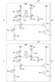
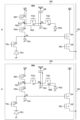
- 2 is a diagram illustrating an example of a circuit configuration of a pixel provided in the solid-state imaging device according to the first embodiment;
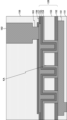
- 3 is a cross-sectional view showing an example of a capacitor configuration applied to the solid-state imaging device according to the first embodiment;
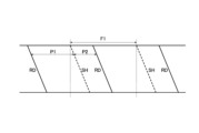
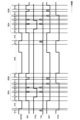
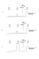
- 5 is a timing chart showing an example of a relationship between a read operation and a shutter operation of the solid-state imaging device according to the first embodiment.
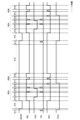
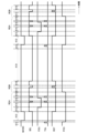
- FIG. 5 is a timing chart showing an example of waveforms of each part in a read operation, a shutter operation, and a storage operation of the solid-state imaging device according to the first embodiment.
- 10 is a timing chart showing an example of waveforms of each part in a read operation, a shutter operation, and a storage operation of a solid-state imaging device according to a second embodiment.
- 13 is a timing chart showing an example of waveforms of each part in a read operation, a shutter operation, and a storage operation of a solid-state imaging device according to a third embodiment.
- FIG. 13 is a diagram illustrating an example of a circuit configuration of a pixel provided in a solid-state imaging device according to a fourth embodiment.
- FIG. 13A and 13B are diagrams illustrating an example of potentials in a pre-accumulation period and an accumulation period of a solid-state imaging device according to a fourth embodiment.
- 13 is a timing chart showing an example of waveforms of each part in a read operation, a shutter operation, and a storage operation of a solid-state imaging device according to a fourth embodiment.
- FIG. 13 is a diagram illustrating an example of a circuit configuration of a pixel provided in a solid-state imaging device according to a fifth embodiment.
- 13 is a timing chart showing an example of waveforms of each part in a read operation, a shutter operation, and a storage operation of a solid-state imaging device according to a fifth embodiment.
- FIG. 13 is a diagram illustrating an example of a circuit configuration of a pixel provided in a solid-state imaging device according to a sixth embodiment.
- FIG. 23 is a diagram illustrating an example of a circuit configuration of a pixel provided in a solid-state imaging device according to a seventh embodiment. 23 is a timing chart showing an example of the relationship between a read operation and a shutter operation of a solid-state imaging device according to a seventh embodiment.
- 13A to 13C are diagrams illustrating a first example of potentials in a vertical blanking period and an accumulation period of a solid-state imaging device according to a seventh embodiment.
- FIG. 13A to 13C are diagrams illustrating a first example of potentials in a vertical blanking period and an accumulation period of a solid-state imaging device according to a seventh embodiment.
- 13A to 13C are diagrams illustrating a first example of potentials in a vertical blanking period and an accumulation period of a solid-state imaging device according to a seventh embodiment.
- FIG. 23 is a diagram showing a second example of potentials in a vertical blanking period and an accumulation period of a solid-state imaging device according to the seventh embodiment.
- FIG. 23 is a diagram showing a second example of potentials in a vertical blanking period and an accumulation period of the solid-state imaging device according to the seventh embodiment.
- FIG. 23 is a diagram showing a third example of potentials in a vertical blanking period and an accumulation period of a solid-state imaging device according to the seventh embodiment.
- FIG. 23 is a diagram showing a third example of potentials in a vertical blanking period and an accumulation period of a solid-state imaging device according to the seventh embodiment.
- FIG. 23 is a diagram illustrating an example of a potential during an accumulation period of a solid-state imaging device according to an eighth embodiment.
- FIG. 23 is a diagram illustrating an example of a circuit configuration of a pixel provided in a solid-state imaging device according to a ninth embodiment.
- FIG. 23 is a cross-sectional view showing an example of the configuration of a pixel provided in a solid-state imaging device according to a tenth embodiment.
- FIG. 23 is a diagram showing a third example of potentials in a vertical blanking period and an accumulation period of a solid-state imaging device according to the seventh embodiment.
- FIG. 23 is a diagram showing a third example
- FIG. 23 is a perspective view showing an example of a stack of a pixel array unit according to an eleventh embodiment
- 1 is a block diagram showing a schematic configuration example of a vehicle control system
- FIG. 4 is an explanatory diagram showing an example of an installation position of an imaging unit.
- First embodiment an example in which a reset transistor and a pass transistor are turned on during the entire period from a read operation to a shutter operation in a pixel provided with photodiodes having different sensitivities
- Second embodiment an example in which a reset transistor and a pass transistor are turned on midway through a period from a read operation to a shutter operation in a pixel provided with photodiodes having different sensitivities
- Third embodiment an example in which a reset transistor and a pass transistor are intermittently turned on during a period from a read operation to a shutter operation in a pixel provided with photodiodes having different sensitivities
- Fourth embodiment an example in which a reset transistor and a pass transistor are turned on during a period between a read operation and a shutter operation in a pixel in which photodiodes having different sensitivities are provided and a transfer transistor is connected to each photodiode
- Fifth embodiment an example in which a reset transistor and a pass transistor are turned on during a period between a read operation and a shutter operation in a pixel provided with a photodiode and a lateral overflow integration capacitor (LOFIC) 6.
- LFIC lateral overflow integration capacitor
- FIG. 1 is a diagram illustrating an example of the configuration of an imaging apparatus according to a first embodiment.
- the imaging device 100 includes an optical system 101, a solid-state imaging device 102, an imaging control unit 103, an image processing unit 104, a storage unit 105, a display unit 106, and an operation unit 107.
- the imaging control unit 103, the image processing unit 104, the storage unit 105, the display unit 106, and the operation unit 107 are connected to each other via a bus 108.
- the imaging device 100 may be used as a standalone device, or may be incorporated into a mobile terminal such as a smartphone, an authentication device, a monitoring device, a vehicle, or a drone.
- the optical system 101 allows light from a subject to be incident on the solid-state imaging device 102, and forms an optical image on the light receiving surface of the solid-state imaging device 102.
- the optical system 101 may include, for example, a focus lens, a zoom lens, and an aperture.
- the optical system 101 may also include multiple lenses, such as a wide-angle lens, a standard lens, and a telephoto lens.
- the solid-state imaging device 102 converts the optical image formed on the light receiving surface into an electrical signal for each pixel, digitizes the electrical signal, and outputs it.
- the solid-state imaging device 102 is, for example, a CMOS (Complementary Metal Oxide Semiconductor) image sensor.
- the CMOS image sensor may be a back-illuminated image sensor or a front-illuminated image sensor. Note that the application of this technology is not limited to the solid-state imaging device 102, and may also be applied to light detection devices such as ToF (Time of Flight) sensors and event detection sensors.
- ToF Time of Flight
- the imaging control unit 103 controls imaging by the solid-state imaging device 102 based on commands from the operation unit 107. At this time, the imaging control unit 103 can control the exposure time, exposure amount, imaging timing, etc. of the solid-state imaging device 102.
- the image processing unit 104 performs image processing based on the output from the solid-state imaging device 102.
- the image processing includes, for example, gamma correction, white balance processing, sharpness processing, and tone conversion processing.
- the image processing unit 104 may include a processor that executes processing based on software.
- the storage unit 105 stores images captured by the solid-state imaging device 102, and stores imaging parameters of the solid-state imaging device 102.
- the storage unit 105 can also store programs that operate the imaging device 100 based on software.
- the storage unit 105 may include a ROM (Read Only Memory), a RAM (Random Access Memory), and a memory card.
- the display unit 106 displays captured images and various information that supports the imaging operation.
- the display unit 106 may be a liquid crystal display or an organic EL (Electro Luminescence) display.
- the operation unit 107 provides a user interface for operating the imaging device 100.
- the operation unit 107 may include, for example, buttons, dials, and switches provided on the imaging device 100.
- the operation unit 107 may be configured as a touch panel together with the display unit 106.
- the imaging device 100 may have additional functions that are not disclosed.
- FIG. 2 is a block diagram showing an example of the configuration of a solid-state imaging device according to the first embodiment.
- the solid-state imaging device 102 includes a pixel array section 111, a vertical scanning circuit 112, a column readout circuit 113, a column signal processing section 114, a horizontal scanning circuit 115, and a control circuit 116.
- the pixel array unit 111 includes a plurality of pixels 120.
- the pixels 120 are arranged in a matrix along the row direction (also called the horizontal direction) and the column direction (also called the vertical direction).
- Each pixel 120 includes a capacitor that accumulates charge overflowing from a photodiode. This capacitor may be a horizontal overflow accumulation capacitance.
- Each pixel 120 may include a plurality of photodiodes with different sensitivities.
- each pixel 120 can form a source follower between itself and the column readout circuit 113 when reading out a signal.
- Each pixel 120 is connected to a horizontal drive line 131 for each row, and to a vertical signal line 132 for each column.
- the horizontal drive line 131 drives each pixel 120 for each row when reading out a signal from each pixel 120.
- the vertical signal line 132 transmits a potential based on a current that flows when reading out a signal from the pixel 120 to the column signal processing unit 114 for each column.
- the vertical scanning circuit 112 scans the pixels 120 to be read in the column direction.
- the vertical scanning circuit 112 may be configured using a vertical register.
- the column readout circuit 113 can form a source follower with each pixel 120 when reading out a signal from the pixel 120. At this time, the column readout circuit 113 can change the potential of the vertical signal line 132 based on the charge held in the pixel 120.
- the column signal processing unit 114 processes signals transmitted in the column direction from each pixel 120.
- the column signal processing unit 114 can perform correlated double sampling (CDS) processing based on the signals transmitted in the column direction from each pixel 120.
- CDS correlated double sampling
- AD Analog to Digital
- the column signal processing unit 114 includes a column ADC unit 114A.
- the column ADC unit 114A can perform AD conversion processing in parallel for each column. At this time, the column ADC unit 114A can perform AD conversion for each column based on the comparison result between the pixel signal read out from the pixel 120 and the reference signal.
- the horizontal scanning circuit 115 scans the pixels 120 to be read in the row direction.
- the horizontal scanning circuit 115 may be configured using a horizontal register.
- the control circuit 116 controls the vertical scanning circuit 112, the column readout circuit 113, the column signal processing unit 114, and the horizontal scanning circuit 115.
- the control circuit 116 can control the scanning timing in the column direction, the scanning timing in the row direction, the operation timing of the column readout circuit 113, and the processing timing of the column signal processing unit 114.
- the control circuit 116 can also control the voltage applied to the capacitor of each pixel 120 so that no voltage is applied to the capacitor during a pre-accumulation period before the accumulation period in which charge is accumulated in the photodiode of each pixel 120.
- the pre-accumulation period can be set to at least a portion of the period between the read operation in which the pixel voltage is read from the pixel 120 and the shutter operation.
- the control circuit 116 is an example of a control unit described in the claims.
- FIG. 3 is a diagram showing an example of the circuit configuration of a pixel provided in a solid-state imaging device according to the first embodiment.
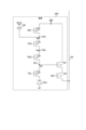
- pixel 120 includes photodiodes PD1 and PD2, transfer transistor 122, reset transistor 123, amplifier transistor 124, selection transistor 125, and floating diffusions FD1 to FD3. Furthermore, pixel 120 includes capacitor 126, pass transistor 127, and switching transistor 128. Transfer transistor 122, reset transistor 123, amplifier transistor 124, selection transistor 125, pass transistor 127, and switching transistor 128 may be MOS (Metal Oxide Semiconductor) transistors. Capacitor 126 may be a MIM (Metal Insulation Metal) capacitor. Capacitor 126 may be a three-dimensional MIM capacitor. Note that pass transistor 127 is an example of a first transistor as defined in the claims. Reset transistor 123 is an example of a second transistor as defined in the claims.
- the pixel 120 is provided with nodes N1 to N3.
- Floating diffusions FD1 to FD3 are formed in the nodes N1 to N3, respectively.
- the photodiodes PD1 and PD2 perform photoelectric conversion and accumulate the photoelectrically converted charges.
- the photodiodes PD1 and PD2 have different sensitivities.
- the sensitivity of the photodiode PD2 can be made smaller than the sensitivity of the photodiode PD1.
- the planar size of the photodiode PD2 can be made smaller than the planar size of the photodiode PD1.
- the photodiodes PD1 and PD2 are an example of a photoelectric conversion unit as described in the claims.
- Capacitor 126 accumulates charge that overflows from photodiode PD2.
- Capacitor 126 may be light-shielded. One end of capacitor 126 is connected to control power supply voltage MVDD, and the other end of capacitor 126 is connected to node N3. In addition, the cathode of photodiode PD2 is connected to node N3.
- Capacitor 126 may be a high-dielectric capacitor with a relative dielectric constant higher than a predetermined value (e.g., 100).
- the transfer transistor 122 transfers the charge accumulated in the photodiode PD1 to the floating diffusion FD1.
- the reset transistor 123 resets the floating diffusions FD1 to FD3.
- the amplification transistor 124 outputs a signal according to the potentials of the floating diffusions FD1 to FD3.
- the selection transistor 125 selects the output of the amplification transistor 124.
- the path transistor 127 sets a path for the charge accumulated in the capacitor 126 to be transferred to the floating diffusion FD1.
- the switching transistor 128 switches the conversion efficiency in the amplification transistor 124.
- the transfer transistor 122 is connected between the cathode of the photodiode PD1 and the node N1.
- the amplification transistor 124 and the selection transistor 125 are connected in series.
- the drain of the amplification transistor 124 is connected to the power supply voltage VDD.
- the gate of the amplification transistor 124 is connected to the node N1.
- the source of the selection transistor 125 is connected to the vertical signal line 132.
- the pass transistor 127 is connected between the nodes N2 and N3.
- the switching transistor 128 is connected between the nodes N1 and N2.
- the reset transistor 123 is connected between the node N2 and the power supply voltage VDD. At this time, the reset transistor 123 and the switching transistor 128 are connected in series.
- a transfer signal TGL is applied to the gate of the transfer transistor 122.
- a reset signal RST is applied to the gate of the reset transistor 123.
- a selection signal SEL is applied to the gate of the selection transistor 125.
- a pass setting signal FCG is applied to the gate of the pass transistor 127.
- a switching signal FDG is applied to the gate of the switching transistor 128.
- the transfer signal TGL, reset signal RST, selection signal SEL, pass setting signal FCG, and switching signal FDG can be transmitted to each pixel 120 via the horizontal drive line 131 in FIG. 2.
- the voltage applied to the capacitor 126 is controlled so that no voltage is applied to the capacitor 126.
- the reset signal RST and the pass setting signal FCG rise, and the reset transistor 123 and the pass transistor 127 are turned on.
- the capacitor 126 is connected to the power supply voltage VDD via the reset transistor 123 and the pass transistor 127 (R1A).
- the control power supply voltage MVDD can be set to the power supply voltage VDD.
- the power supply voltage VDD is applied to both ends of the capacitor 126, and the voltage applied to the capacitor 126 is controlled so that no voltage is applied to the capacitor 126. Therefore, it is possible to prevent charge from being accumulated in the capacitor 126 before the start of the accumulation period, and it is possible to suppress the potential fluctuation of the node N3 caused by the dielectric absorption of the capacitor 126.
- Turning a transistor on refers to a state in which the voltage applied to the transistor's terminals exceeds the transistor's threshold voltage.
- Turning a transistor off refers to a state in which the voltage applied to the transistor's terminals does not exceed the transistor's threshold voltage, and leakage current conduction is permitted even when the transistor is off.
- capacitor 126 is set to a floating state. At this time, as shown in b in the figure, after the shutter operation, the path setting signal FCG falls and the path transistor 127 turns off. At this time, capacitor 126 is disconnected from the power supply voltage VDD and transitions to a floating state. When capacitor 126 transitions to a floating state, the charge that has overflowed from photodiode PD2 is accumulated in capacitor 126 (R1B).
- FIG. 4 is a cross-sectional view showing an example of a capacitor configuration applied to a solid-state imaging device according to the first embodiment. Note that the drawings used in the following explanation may differ in scale and shape from the actual structure in order to make each configuration easier to understand.
- a wiring layer 161 is embedded in an interlayer insulating layer 151.
- a passivation layer 152 is laminated on the wiring layer 161, and an interlayer insulating layer 153 is laminated on the passivation layer 152.
- An opening KA is formed in the passivation layer 152 and the interlayer insulating layer 153 to expose the wiring layer 161.
- a capacitance electrode 154 is formed on the interlayer insulating layer 153 so as to cover the bottom and side surfaces of the opening KA.
- a dielectric layer 155 is formed on the capacitance electrode 154 so as to cover the bottom and side surfaces of the capacitance electrode 154.
- a capacitance electrode 156 is formed on the dielectric layer 155 so as to cover the bottom and side surfaces of the dielectric layer 155.
- the capacitance electrodes 154, 156 and the dielectric layer 155 can be used as the capacitor 126. At this time, the capacitor 126 can constitute a three-dimensional MIM.
- a passivation layer 157 is formed on the dielectric layer 155 so as to cover the capacitance electrode 156.
- An interlayer insulating layer 158 is stacked on the passivation layer 157.
- a wiring layer 162 is embedded in the interlayer insulating layer 158. The wiring layer 162 is connected to the capacitance electrode 156 through the via 163.
- the materials for the wiring layers 161, 162, the vias 163, and the capacitance electrodes 154, 156 can be, for example, Cu, Ti, Ta, Al, W, Ni, Ru, Co, TiN, TaN, and WN, and may be a layered structure of multiple materials.
- the material of the dielectric layer 155 may be, for example, SiO2 , SiON, Si3N4 , hafnium oxide ( HfO2 ), aluminum oxide ( Al2O3 ), zirconium oxide (ZrO), tantalum oxide ( Ta2O5 ), titanium oxide ( TiO2 ), lanthanum oxide ( LaO3 ), yttrium oxide ( Y2O3 ), aluminum nitride (AlN), hafnium oxynitride (HfON), aluminum oxynitride (AlON), or a laminate structure of multiple materials may be used.
- the interlayer insulating layers 151 and 158 may be made of inorganic materials such as SiO2 , SiON, SiOC, Si3N4 , or SiCO, or organic materials having a skeleton of polyimide, acrylic, silicone, or epoxy group, or may have a laminated structure of multiple materials.
- the passivation layers 152 and 157 may be made of an organic material having a skeleton of polyimide, acrylic, silicone, or epoxy group, or a material containing a filler such as SiO 2 , Al 2 O 3 , AlN, or BN.
- the passivation layers 152 and 157 may be a CVD (Chemical Vapor Deposition) film or a sputtered film.
- FIG. 5 is a timing chart showing an example of the relationship between the read operation and the shutter operation of the solid-state imaging device according to the first embodiment.
- the solid-state imaging device repeats a shutter operation SH for each frame F1. At this time, the solid-state imaging device performs a read operation RD between the shutter operations SH in each frame F1.
- an accumulation period P2 is set from the shutter operation SH of each frame F1 to the read operation RD. Also, a pre-accumulation period P1 is set from the read operation RD to the shutter operation SH of the next frame F1.
- the voltage applied to capacitor 126 is controlled so that no voltage is applied to capacitor 126.
- reset transistor 123 and pass transistor 127 are turned on during at least a portion of the period between read operation RD and shutter operation SH.
- the capacitor 126 is set to a floating state. At this time, as shown in FIG. 3b, the pass transistor 127 is turned off.
- FIG. 6 is a timing chart showing an example of waveforms of each part during the read operation, shutter operation, and accumulation operation of the solid-state imaging device according to the first embodiment.
- the shutter period K11 begins.
- the control power supply voltage MVDD is set to the power supply voltage VDD.
- the selection signal SEL is set to a low level.
- the switching signal FDG, the reset signal RST, and the path setting signal FCG are set to a high level.
- the transfer signal TGL rises, and the charges in the photodiode 121 and the floating diffusions FD1 and FD3 are discharged, and the conversion efficiency in the amplification transistor 124 is reduced.
- the accumulation period K12 begins.
- the control power supply voltage MVDD falls and is set to an intermediate potential.
- the intermediate potential can be set to a voltage lower than the power supply voltage VDD.
- the dark current of the capacitor 126 can be reduced by setting the control power supply voltage MVDD to an intermediate potential.
- the reset signal RST falls and the selection signal SEL rises.
- the reset transistor 123 turns off and the selection transistor 125 turns on, and the potential of the vertical signal line 132 is set based on the source follower operation when the low-efficiency P-phase level of the floating diffusion FD1 is applied to the gate of the amplification transistor 124.
- the low-efficiency P-phase level is AD converted based on the potential of the vertical signal line 132 at that time.
- the switching signal FDG falls, and the conversion efficiency of the amplification transistor 124 increases.
- the potential of the vertical signal line 132 is set based on the source follower operation when the high-efficiency P-phase level of the floating diffusion FD1 is applied to the gate of the amplification transistor 124.
- the high-efficiency P-phase level is AD converted based on the potential of the vertical signal line 132 at that time.
- the selection signal SEL falls and the transfer signal TGL rises.
- the selection transistor 125 turns off and the transfer transistor 122 turns on, and the charge stored in the photodiode PD1 is transferred to the floating diffusion FD1.
- the selection signal SEL rises and the transfer signal TGL falls.
- the selection transistor 125 turns on and the transfer transistor 122 turns off, and the potential of the vertical signal line 132 is set based on the source follower operation when the high-efficiency D-phase level of the floating diffusion FD1 is applied to the gate of the amplification transistor 124.
- the high-efficiency D-phase level is AD converted based on the potential of the vertical signal line 132 at that time.
- the switching signal FDG rises, and the conversion efficiency of the amplification transistor 124 decreases. Furthermore, the selection signal SEL falls and the transfer signal TGL rises. At this time, the selection transistor 125 turns off and the transfer transistor 122 turns on, and the charge stored in the photodiode PD1 is transferred to the floating diffusion FD1.
- the selection signal SEL rises and the transfer signal TGL falls.
- the selection transistor 125 turns on and the transfer transistor 122 turns off, and the potential of the vertical signal line 132 is set based on the source follower operation when the low-efficiency D-phase level of the floating diffusion FD1 is applied to the gate of the amplification transistor 124.
- the low-efficiency D-phase level is AD converted based on the potential of the vertical signal line 132 at that time.
- the reset signal RST rises.
- the reset transistor 123 turns on, and the charge in the floating diffusions FD1 and FD2 is discharged.
- CDS read RDA can be performed during the low-efficiency P-phase single read period K13, the high-efficiency P-phase single read period K14, the high-efficiency D-phase single read period K15, and the low-efficiency D-phase single read period K16.
- the reset signal RST falls and the path setting signal FCG rises.
- the reset transistor 123 turns off and the path transistor 127 turns on, and the potential of the vertical signal line 132 is set based on the source follower operation when the D-phase level of the floating diffusion FD3 is applied to the gate of the amplification transistor 124. Then, based on the potential of the vertical signal line 132 at that time, the D-phase level is AD converted.
- the selection signal SEL falls and the reset signal RST rises.
- the selection transistor 125 turns off and the reset transistor 123 turns on, discharging the charge in the floating diffusions FD1 to FD3.
- the reset signal RST falls and the selection signal SEL rises.
- the reset transistor 123 turns off and the selection transistor 125 turns on, and the potential of the vertical signal line 132 is set based on the source follower operation when the P-phase level of the floating diffusion FD3 is applied to the gate of the amplification transistor 124.
- the P-phase level is AD converted.
- the DDS read RDB can be performed.
- the voltage applied to capacitor 126 is controlled so that no voltage is applied to capacitor 126.
- the reset signal RST rises.
- the control power supply voltage MVDD is maintained at the power supply voltage VDD.
- the reset transistor 123 and the path transistor 127 are turned on, and the power supply voltage VDD is applied to both ends of capacitor 126.
- the voltage applied to capacitor 126 is controlled so that no voltage is applied to capacitor 126.
- reset transistor 123 and pass transistor 127 are turned on during the period between the read operation and the shutter operation. This makes it possible to control the voltage applied to capacitor 126 so that no voltage is applied to capacitor 126 during pre-accumulation period K19. This makes it possible to prevent charge from accumulating in capacitor 126 before the start of accumulation period PK11, and suppresses image retention and deterioration of linearity caused by dielectric absorption of capacitor 126.
- reset transistor 123 and pass transistor 127 are turned on for the entire period from readout operation to shutter operation.
- reset transistor 123 and pass transistor 127 are turned on midway through the period from readout operation to shutter operation.
- FIG. 7 is a timing chart showing an example of waveforms of each part during the read operation, shutter operation, and accumulation operation of the solid-state imaging device according to the second embodiment.
- a pre-accumulation period K29 is provided instead of the pre-accumulation period K19 in the first embodiment described above.
- Other operations of the solid-state imaging device of the second embodiment are similar to those of the solid-state imaging device of the first embodiment described above.
- the voltage applied to the capacitor 126 is controlled so that no voltage is applied to the capacitor 126 from the middle of the period from the read operation to the shutter operation.
- the control power supply voltage MVDD falls and is set to an intermediate potential
- the path setting signal FCG falls.
- the control power supply voltage MVDD also rises and is set to the power supply voltage VDD.
- the reset transistor 123 and the path transistor 127 are turned on, and the power supply voltage VDD is applied to both ends of the capacitor 126.
- the voltage applied to the capacitor 126 is controlled so that no voltage is applied to the capacitor 126 during a part of the pre-accumulation period K29.
- reset transistor 123 and pass transistor 127 are turned on midway through the period from the readout operation to the shutter operation. This makes it possible to prevent voltage from being applied to capacitor 126 during part of pre-accumulation period K29, and suppresses degradation of the reliability of capacitor 126 while suppressing afterimages and deterioration of linearity caused by dielectric absorption of capacitor 126.
- reset transistor 123 and pass transistor 127 are turned on during the entire period from read operation to shutter operation.
- reset transistor 123 and pass transistor 127 are turned on intermittently during the period from read operation to shutter operation.
- FIG. 8 is a timing chart showing an example of waveforms of each part during the read operation, shutter operation, and storage operation of a solid-state imaging device according to the third embodiment.
- a pre-accumulation period K39 is provided instead of the pre-accumulation period K19 in the first embodiment described above.
- Other operations of the solid-state imaging device of the third embodiment are similar to those of the solid-state imaging device of the first embodiment described above.
- the voltage applied to the capacitor 126 is intermittently controlled so that no voltage is applied to the capacitor 126 during the period from the read operation to the shutter operation.
- the path setting signal FCG falls.
- the path setting signal FCG and the reset signal RST rise in a pulsed manner.
- the number of times that the path setting signal FCG and the reset signal RST rise in a pulsed manner during the pre-accumulation period K39 may be one or multiple.
- the reset transistor 123 and the path transistor 127 are intermittently turned on, and the power supply voltage VDD is intermittently applied to both ends of the capacitor 126.
- the voltage applied to the capacitor 126 is controlled so that no voltage is applied to the capacitor 126 during part of the pre-accumulation period K39.
- reset transistor 123 and pass transistor 127 are intermittently turned on during the period from the read operation to the shutter operation. This makes it possible to prevent voltage from being intermittently applied to capacitor 126 during pre-accumulation period K39, making it possible to suppress shutter step while suppressing afterimages and deterioration of linearity caused by dielectric absorption of capacitor 126.
- the reset transistor 123 and the pass transistor 127 are turned on during the period from the readout operation to the shutter operation.
- the reset transistor 123 and the pass transistor 127 are turned on during the period from the readout operation to the shutter operation.
- FIG. 9 is a diagram showing an example of the circuit configuration of a pixel provided in a solid-state imaging device according to the fourth embodiment.
- pixel 220 is the pixel 120 of the first embodiment described above, to which a transfer transistor 129 has been added.
- the rest of the configuration of the pixel of the fourth embodiment is the same as the configuration of pixel 120 of the first embodiment described above.
- the transfer transistor 129 is connected between the cathode of the photodiode PD2 and the node N3.
- a transfer signal TGS is applied to the gate of the transfer transistor 129.
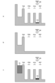
- FIG. 10 is a diagram showing an example of the potential during the pre-accumulation period and accumulation period of a solid-state imaging device according to the fourth embodiment.
- “a” shows an example of the potential during the pre-accumulation period.
- “b” shows an example of the potential during the shutter period.
- “c” shows an example of the potential during the accumulation period.
- the voltage VC applied to the capacitor 126 is controlled so that no voltage is applied to the capacitor 126.
- the reset signal RST and the pass setting signal FCG are set to a high level.
- the reset transistor 123 and the pass transistor 127 are turned on, and the potential from the capacitor 126 to the power supply voltage VDD is set so that the charge EL is not accumulated in the capacitor 126.
- the transfer signal TGS is set to a low level, and the transfer transistor 129 is turned off. As a result, charge is accumulated in the photodiode PD2 based on the incidence of light on the photodiode PD2.
- capacitor 126 is set to a floating state.
- the path setting signal FCG is set to a low level, and path transistor 127 is turned off.
- the charge that overflows from photodiode PD2 is accumulated in capacitor 126.
- FIG. 11 is a timing chart showing an example of waveforms of each part during the read operation, shutter operation, and storage operation of a solid-state imaging device according to the fourth embodiment.
- a P-phase sub-readout period K41 and a D-phase sub-readout period K42 are added to the readout operation of the first embodiment described above.
- the other operations of the pixel 220 of the fourth embodiment are similar to the operations of the pixel 120 of the first embodiment described above.
- the selection signal SEL falls and the selection transistor 125 turns off. Then, the reset signal RST falls and the path setting signal FCG rises, and then the P-phase sub-read period K41 begins.
- the selection signal SEL rises.
- the selection transistor 125 turns on, and the potential of the vertical signal line 132 is set based on the source follower operation when the P-phase sub-level of the floating diffusion FD3 is applied to the gate of the amplification transistor 124. Then, the P-phase sub-level is AD converted based on the potential of the vertical signal line 132 at that time.
- the selection signal SEL falls and the transfer signal TGS rises.
- the selection transistor 125 turns off and the transfer transistor 129 turns on, and the charge stored in the photodiode PD2 is transferred to the floating diffusion FD3.
- the selection signal SEL rises and the transfer signal TGS falls.
- the selection transistor 125 turns on and the transfer transistor 129 turns off, and the potential of the vertical signal line 132 is set based on the source follower operation when the D-phase sub-level of the floating diffusion FD2 is applied to the gate of the amplification transistor 124.
- the D-phase sub-level is AD converted based on the potential of the vertical signal line 132 at that time.
- the D-phase batch read period K17 begins.
- a CDS read RDC can be performed.
- reset transistor 123 and pass transistor 127 are turned on during the period from read operation to shutter operation. This makes it possible to read out a signal individually from photodiode PD2 while preventing voltage from being applied to capacitor 126 during pre-accumulation period K19. This makes it possible to expand the dynamic range while suppressing image retention and deterioration of linearity caused by dielectric absorption of capacitor 126.
- the full-period shutter operation of the pre-accumulation period K19 in the above-mentioned first embodiment is taken as an example, but the partial-period shutter operation in the above-mentioned second embodiment may also be applied, or the intermittent shutter operation in the above-mentioned third embodiment may also be applied.
- reset transistor 123 and pass transistor 127 are turned on during the period from the read operation to the shutter operation.
- reset transistor 123 and pass transistor 127 are turned on during the period from the read operation to the shutter operation.
- FIG. 12 is a diagram showing an example of the circuit configuration of a pixel provided in a solid-state imaging device according to the fifth embodiment.
- the photodiode PD2 of the first embodiment described above is removed from the pixel 320.
- the capacitor 126 can operate as a horizontal overflow storage capacitance that stores the charge that overflows from the photodiode PD1.
- the rest of the configuration of the pixel 320 of the fifth embodiment is the same as the configuration of the pixel 120 of the first embodiment described above.
- FIG. 13 is a timing chart showing an example of waveforms of each part during the read operation, shutter operation, and accumulation operation of a solid-state imaging device according to the fifth embodiment.
- the reset signal RST is maintained at a low level during the transition from the low-efficiency D-phase individual read period K16 to the D-phase batch read period K17.
- the transition to the D-phase batch read period K17 occurs while the charges of the floating diffusions FD1 and FD2 are maintained.
- the potential of the vertical signal line 132 is set based on the source follower operation when the D-phase level of the floating diffusions FD1 to FD3 is applied to the gate of the amplification transistor 124.
- the D-phase level is AD converted based on the potential of the vertical signal line 132 at that time.
- Other operations of the pixel 320 of the fifth embodiment are similar to those of the pixel 120 of the first embodiment described above.
- reset transistor 123 and pass transistor 127 are turned on during the period from the read operation to the shutter operation.
- This makes it possible to operate capacitor 126 as a horizontal overflow storage capacitance that stores charge that overflows from photodiode PD1 while preventing voltage from being applied to capacitor 126 during pre-accumulation period K19. This makes it possible to expand the dynamic range while suppressing image retention and deterioration of linearity caused by dielectric absorption of capacitor 126.
- the full-period shutter operation of the pre-accumulation period K19 in the above-mentioned first embodiment is taken as an example, but the partial-period shutter operation in the above-mentioned second embodiment may also be applied, or the intermittent shutter operation in the above-mentioned third embodiment may also be applied.
- the reset transistor 123 and the pass transistor 127 are turned on during the period from the readout operation to the shutter operation.
- the reset transistor 123 and the pass transistor 127 are turned on during the period from the readout operation to the shutter operation.
- FIG. 14 is a diagram showing an example of the circuit configuration of a pixel provided in a solid-state imaging device according to the sixth embodiment.
- pixel 420 is obtained by adding an overflow control transistor 130 to pixel 320 of the fifth embodiment described above.
- the rest of the configuration of pixel 420 of the sixth embodiment is the same as the configuration of pixel 120 of the first embodiment described above.
- the overflow control transistor 130 is connected between the photodiode PD1 and the capacitor 126.
- An overflow control voltage OFG is applied to the gate of the overflow control transistor 130.
- the overflow control voltage OFG can control the overflow of charge from the photodiode PD1 to the capacitor 126.
- the overflow control voltage OFG may be a fixed voltage.
- the read operation of this pixel 420 is similar to the read operation of the pixel 320 in the fifth embodiment described above.
- the reset transistor 123 and the pass transistor 127 are turned on during the period from the read operation to the shutter operation. This makes it possible to control the overflow of charge from the photodiode PD1 while preventing a voltage from being applied to the capacitor 126 during the pre-accumulation period K19. This makes it possible to expand the dynamic range while suppressing image retention and deterioration of linearity caused by the dielectric absorption of the capacitor 126.
- the full-period shutter operation of the pre-accumulation period K19 in the first embodiment described above is taken as an example, but the partial-period shutter operation in the second embodiment described above may also be applied, or the intermittent shutter operation in the third embodiment described above may also be applied.
- the capacitor 126 is reset during the pre-accumulation period. In the seventh embodiment, the capacitor 126 is reset during the accumulation period.
- FIG. 15 is a diagram showing an example of the circuit configuration of a pixel provided in a solid-state imaging device according to the seventh embodiment.
- pixel 520 is obtained by removing photodiode PD2 from pixel 120 of the first embodiment described above.
- reset transistor 123 is connected between power supply voltage VDD and node N3.
- the rest of the configuration of pixel 520 of the seventh embodiment is the same as the configuration of pixel 120 of the first embodiment described above.
- the capacitor 126 can be reset without turning on the pass transistor 127.
- the capacitor 126 can be reset without discharging the charge stored in the floating diffusion FD2.
- the switching transistor 128 can be turned on to increase the capacitance of the stage preceding the pass transistor 127. Therefore, the capacitor 126 can be reset during the accumulation period while suppressing a decrease in the dynamic range.
- the reset transistor 123 is an example of a third transistor in one embodiment of the present disclosure.
- control circuit 116 can control the driving of the switching transistor 128, the pass transistor 127, and the reset transistor 123. At this time, the control circuit 116 can turn on the reset transistor 123 for at least a portion of the accumulation period in the photodiode PD1. Furthermore, when the control circuit 116 turns on the reset transistor 123 for at least a portion of the accumulation period in the photodiode PD1, it can turn on the switching transistor 128 and turn off the pass transistor 127.
- FIG. 16 is a timing chart showing an example of the relationship between the read operation and the shutter operation of a solid-state imaging device according to the seventh embodiment.
- the solid-state imaging device repeats a shutter operation SH and a sub-shutter operation MSH for each frame F1.
- Each frame F1 is provided with an accumulation period K1 and a vertical blanking period K2.
- the solid-state imaging device performs a sub-shutter operation MSH during the accumulation period K1 in each frame F1.
- an accumulation period K1 is set from the shutter operation SH of each frame F1 to the read operation RD. Also, a vertical blanking period K2 is set from the read operation RD to the shutter operation SH of the next frame F1.
- the solid-state imaging device turns on the switching transistor 128, turns off the pass transistor 127, and turns on the reset transistor 123. At this time, the solid-state imaging device can reset the capacitor 126 without discharging the charge stored in the floating diffusion FD2.
- FIGS. 17 to 19 are diagrams showing a first example of potentials during the vertical blanking period and accumulation period of a solid-state imaging device according to the seventh embodiment. Note that FIG. 17 to FIG. 19 show an example in which the signal charge accumulated before the sub-shutter operation MSH is less than the maximum number of electrons FDQ that can be received at a stage preceding the pass transistor 127.
- the switching transistor 128, the pass transistor 127, and the reset transistor 123 are turned on. At this time, the recovery voltage ES caused by the dielectric absorption of the capacitor 126 is reset at the node N3.
- the switching transistor 128 is turned on.
- the nodes N1 and N2 are coupled, and the capacitance between the nodes N1 and N2 is increased.
- the charge EL overflowing from the photodiode PD1 can be stored between the nodes N1 and N2, and the dynamic range can be expanded.
- the number of electrons FDQ that can be received at the stage preceding the pass transistor 127 increases. This number of electrons FDQ is proportional to the potential range and inversely proportional to the conversion efficiency.
- the potential range expands based on the boost caused by turning on the switching transistor 128, and the number of electrons FDQ increases due to the decrease in conversion efficiency caused by the gate capacitance.
- the capacitor 126 can be reset during the accumulation period without reducing the dynamic range.
- the sub-shutter operation MSH may be performed at any timing during the accumulation period K1.
- the reset transistor 123 is turned on while the pass transistor 127 is turned off.
- the charge EL that has overflowed from the photodiode PD1 is stored between the nodes N1 and N2, and the recovery voltage ES caused by the dielectric absorption of the capacitor 126 is reset at the node N3.
- the switching transistor 128 and the reset transistor 123 are turned off. At this time, the coupling between nodes N1 and N2 is released, and the charge EL that has overflowed from the photodiode PD1 is distributed to each of the nodes N1 and N2.
- the charge EL that has overflowed from the photodiode PD1 also overflows from each of the nodes N1 and N2 and is also accumulated in the node N3.
- switching transistor 128 and pass transistor 127 are turned on, and nodes N1 to N3 are coupled.
- FIGS. 20 and 21 are diagrams showing a second example of the potential during the vertical blanking period and accumulation period of the solid-state imaging device according to the seventh embodiment.
- FIG. 20 and FIG. 21 show an example in which the dynamic range corresponding to the maximum number of electrons FDQ that can be received at the stage preceding the pass transistor 127 is equivalent to the dynamic range defined by the circuit side such as the AD converter.
- the sub-shutter operation MSH can be performed at any timing.
- FIG. 22 and FIG. 23 show, as an example, an example in which the sub-shutter operation MSH is performed before the charge generated in the photodiode PD1 flows into the node N3.
- the switching transistor 128 is turned on. At this time, the nodes N1 and N2 are coupled, and the capacitance between the nodes N1 and N2 is increased. The charge EL that overflows from the photodiode PD1 is accumulated between the nodes N1 and N2.
- the charge EL accumulated between nodes N1 and N2 before the sub-shutter operation MSH reaches a value equivalent to the dynamic range.
- the charge EL that has overflowed from the photodiode PD1 remains accumulated between nodes N1 and N2, and the recovery voltage at node N3 due to the dielectric absorption of capacitor 126 is reset.
- the switching transistor 128 and the reset transistor 123 are turned off. At this time, the coupling between nodes N1 and N2 is released, and the charge EL accumulated between nodes N1 and N2 overflows into node N3.
- the charge FE that has exceeded the dynamic range and overflowed from the photodiode PD1 is accumulated in the node N3 via the nodes N1 and N2.
- FIGS. 22 and 23 are diagrams showing a third example of the potential during the vertical blanking period and accumulation period of the solid-state imaging device according to the seventh embodiment.
- FIGS. 22 and 23 show an example in which the dynamic range corresponding to the maximum number of electrons FDQ that can be received at the stage preceding the pass transistor 127 exceeds the dynamic range defined by the circuit side such as the AD converter.
- the sub-shutter operation MSH can be performed at any timing.
- FIGS. 22 and 23 show an example in which the sub-shutter operation MSH is performed after the charge generated in the photodiode PD1 flows into the node N3.
- the switching transistor 128 is turned on. At this time, the nodes N1 and N2 are coupled, and the capacitance between the nodes N1 and N2 is increased. Then, the charge FL that has overflowed from the photodiode PD1 beyond the dynamic range is accumulated in the node N3 via the nodes N1 and N2.
- the reset transistor 123 is turned on while the pass transistor 127 is turned off.
- the charge EL that has overflowed from the photodiode PD1 remains stored between the nodes N1 and N2, and the recovery voltage caused by the dielectric absorption of the capacitor 126 is reset at the node N3.
- the charge FL that has exceeded the dynamic range and has been stored at the node N3 is discharged.
- the switching transistor 128 and the reset transistor 123 are turned off. At this time, the coupling between nodes N1 and N2 is released, and the charge EL accumulated between nodes N1 and N2 overflows into node N3.
- the charge FE that exceeds the dynamic range and overflows from the photodiode PD1 is accumulated in the node N3 via the nodes N1 and N2.
- the switching transistor 128 is turned on, the pass transistor 127 is turned off, and the reset transistor 123 is turned on. This makes it possible to reset the capacitor 126 without discharging the charge accumulated in the floating diffusion FD2. This makes it possible to suppress the degradation of the dynamic range while also suppressing afterimages and deterioration of linearity caused by the dielectric absorption of the capacitor 126.
- the capacitor 126 is reset during the charge accumulation period without discharging the charge accumulated in the floating diffusion FD2.
- the gate voltage of the pass transistor 127 is made variable during the charge accumulation period.
- FIG. 24 shows an example of the potential during the accumulation period of a solid-state imaging device according to the eighth embodiment.
- the negative voltage at the gate of pass transistor 127 may be made variable in order to increase the number of electrons FDQ that can be received at the stage preceding pass transistor 127.
- the potential barrier that accumulates charge EL between nodes N1 and N2 can be made higher, and the number of electrons FDQ that can be received at the stage preceding pass transistor 127 can be increased.
- the gate voltage of the pass transistor 127 is made variable during the accumulation period. This makes it possible to increase the capacity of the floating diffusion that can be accumulated during the accumulation period while resetting the capacitor 126 during the accumulation period.
- the capacitor 126 is reset during the charge accumulation period without discharging the charge accumulated in the floating diffusion FD2.
- a capacitor that is not affected by dielectric absorption is added.
- FIG. 25 is a diagram showing an example of the circuit configuration of a pixel provided in a solid-state imaging device according to the ninth embodiment.
- pixel 620 is pixel 520 of the seventh embodiment described above, to which a capacitor 626 has been added.
- the rest of the configuration of pixel 620 of the ninth embodiment is similar to the configuration of pixel 520 of the seventh embodiment described above.
- Capacitor 626 is connected between node N2 and power supply voltage VDD. Capacitor 626 may be configured to be free from the effects of dielectric absorption, and reading from capacitor 626 may be controlled to be free from the effects of dielectric absorption. For example, capacitor 626 may be made of a material that does not cause polarization in the insulation between the electrodes, and CDS may be implemented for reading from capacitor 626.
- the capacitor 626 which is not affected by dielectric absorption, is connected to node N2. This makes it possible to increase the number of electrons FDQ that can be received at the stage preceding the pass transistor 127 when the capacitor 126 is reset during the accumulation period, thereby making it possible to expand the dynamic range while suppressing the occurrence of afterimages.
- the capacitor 126 is reset during the charge accumulation period without discharging the charge accumulated in the floating diffusion FD2.
- a buried gate is provided in the switching transistor.
- FIG. 26 is a cross-sectional view showing an example of the configuration of a pixel provided in a solid-state imaging device according to the tenth embodiment.
- impurity diffusion layers 721 to 723 are formed in a semiconductor substrate 711 and are separated from each other.
- the material of the semiconductor substrate 711 may be Si, InP, InGaP, InAlP, InGaAs, InAlAs, or a compound semiconductor with a chalcopyrite structure.
- Each of the impurity diffusion layers 721 to 723 may be used as floating diffusions FD1 to FD3.
- a gate electrode 731 is formed on the semiconductor substrate 711 so that its end overlaps the impurity diffusion layer 721.
- a gate electrode 732 is also formed on the semiconductor substrate 711 so as to span between the impurity diffusion layers 721 and 722.
- a gate electrode 733 is also formed on the semiconductor substrate 711 so as to span between the impurity diffusion layers 722 and 723.
- a gate insulating film is formed between the gate electrodes 731 to 733 and the semiconductor substrate 711.
- the gate electrodes 731 to 733 can be used for the transfer transistor 122, the switching transistor 128, and the pass transistor 127, respectively.
- a buried gate 712 is buried in the semiconductor substrate 711.
- the buried gate 712 is connected to a gate electrode 732.
- a gate insulating film is formed between the buried gate 712 and the semiconductor substrate 711.
- a buried gate 712 is provided in the switching transistor 128. This makes it possible to increase the number of electrons FDQ that can be received in the stage preceding the pass transistor 127 when the capacitor 126 is reset during the accumulation period, thereby making it possible to expand the dynamic range while suppressing the occurrence of afterimages.
- a reset transistor 123 and a pass transistor 127 that are turned on during the period between a read operation and a shutter operation are provided in a pixel 120 provided with photodiodes PD1 and PD2 having different sensitivities.
- semiconductor chips provided with a pixel array portion in which pixels are arranged in a matrix are stacked.
- FIG. 27 is a perspective view showing an example of a stack of pixel array parts according to the eleventh embodiment.
- the solid-state imaging device includes semiconductor chips 921 and 922.
- Semiconductor chip 922 is stacked on semiconductor chip 921.
- a pixel array section 923 is formed in the semiconductor chip 922.
- pixels 931 are arranged in a matrix in the row and column directions.
- the pixels 931 may be any of the pixels in the first to sixth embodiments described above.
- a pad electrode 932 and a via electrode 933 are formed around the pixel array section 923.
- the via electrode 933 passes through the semiconductor chip 922 and can electrically connect the semiconductor chips 921 and 922 to each other.
- a peripheral circuit 924 is formed on the semiconductor chip 921.
- a column readout circuit 925, a column ADC 926, a communication interface 927, and a control circuit 928 are formed on the peripheral circuit 924.
- the column readout circuit 925 and the column ADC 926 may be formed to correspond to positions on both sides of the pixel array section 923 in the column direction.
- the control circuit 928 can control the voltage applied to the capacitor of each pixel 931 so that no voltage is applied to the capacitor during a pre-accumulation period before the accumulation period in which charge is accumulated in the photodiode of each pixel 931.
- the pre-accumulation period can be set to at least a portion of the period between the read operation in which the pixel voltage is read out from the pixel 931 and the shutter operation.
- the semiconductor chips 921 and 922 may be directly bonded. Hybrid bonding may be used for directly bonding the semiconductor chips 921 and 922. In this case, the semiconductor chips 921 and 922 may be electrically connected based on a Cu-Cu connection.
- the material of the semiconductor substrate used for the semiconductor chips 921 and 922 may be Si, InGaAs, or InP.
- the semiconductor chip 922 in which the pixel array section 923 is formed is stacked on the semiconductor chip 921 in which the peripheral circuit 924 is formed. This makes it possible to increase the sensitivity of the solid-state imaging device while suppressing an increase in the mounting area of the semiconductor chip in which the solid-state imaging device is formed.
- the technology according to the present disclosure can be applied to various products.
- the technology according to the present disclosure may be realized as a device mounted on any type of moving body such as an automobile, an electric vehicle, a hybrid electric vehicle, a motorcycle, a bicycle, a personal mobility device, an airplane, a drone, a ship, or a robot.
- FIG. 28 is a block diagram showing a schematic configuration example of a vehicle control system, which is an example of a mobile object control system to which the technology disclosed herein can be applied.
- the vehicle control system 12000 includes a plurality of electronic control units connected via a communication network 12001.
- the vehicle control system 12000 includes a drive system control unit 12010, a body system control unit 12020, an outside vehicle information detection unit 12030, an inside vehicle information detection unit 12040, and an integrated control unit 12050.
- Also shown as functional components of the integrated control unit 12050 are a microcomputer 12051, an audio/video output unit 12052, and an in-vehicle network I/F (interface) 12053.
- the drive system control unit 12010 controls the operation of devices related to the drive system of the vehicle according to various programs.
- the drive system control unit 12010 functions as a control device for a drive force generating device for generating the drive force of the vehicle, such as an internal combustion engine or a drive motor, a drive force transmission mechanism for transmitting the drive force to the wheels, a steering mechanism for adjusting the steering angle of the vehicle, and a braking device for generating a braking force for the vehicle.
- the body system control unit 12020 controls the operation of various devices installed in the vehicle body according to various programs.
- the body system control unit 12020 functions as a control device for a keyless entry system, a smart key system, a power window device, or various lamps such as headlamps, tail lamps, brake lamps, turn signals, and fog lamps.
- radio waves or signals from various switches transmitted from a portable device that replaces a key can be input to the body system control unit 12020.
- the body system control unit 12020 accepts the input of these radio waves or signals and controls the vehicle's door lock device, power window device, lamps, etc.
- the outside-vehicle information detection unit 12030 detects information outside the vehicle equipped with the vehicle control system 12000.
- the image capturing unit 12031 is connected to the outside-vehicle information detection unit 12030.
- the outside-vehicle information detection unit 12030 causes the image capturing unit 12031 to capture images outside the vehicle and receives the captured images.
- the outside-vehicle information detection unit 12030 may perform object detection processing or distance detection processing for people, cars, obstacles, signs, characters on the road surface, etc. based on the received images.
- the imaging unit 12031 is an optical sensor that receives light and outputs an electrical signal according to the amount of light received.
- the imaging unit 12031 can output the electrical signal as an image, or as distance measurement information.
- the light received by the imaging unit 12031 may be visible light, or may be invisible light such as infrared light.
- the in-vehicle information detection unit 12040 detects information inside the vehicle.
- a driver state detection unit 12041 that detects the state of the driver is connected.
- the driver state detection unit 12041 includes, for example, a camera that captures an image of the driver, and the in-vehicle information detection unit 12040 may calculate the driver's degree of fatigue or concentration based on the detection information input from the driver state detection unit 12041, or may determine whether the driver is dozing off.
- the microcomputer 12051 can calculate control target values for the driving force generating device, steering mechanism, or braking device based on information inside and outside the vehicle acquired by the outside-vehicle information detection unit 12030 or the inside-vehicle information detection unit 12040, and output control commands to the drive system control unit 12010.
- the microcomputer 12051 can perform cooperative control aimed at realizing the functions of an Advanced Driver Assistance System (ADAS), including vehicle collision avoidance or impact mitigation, following driving based on the distance between vehicles, maintaining vehicle speed, vehicle collision warning, or vehicle lane departure warning.
- ADAS Advanced Driver Assistance System
- the microcomputer 12051 can also perform cooperative control for the purpose of autonomous driving, which allows the vehicle to travel autonomously without relying on the driver's operation, by controlling the driving force generating device, steering mechanism, braking device, etc. based on information about the surroundings of the vehicle acquired by the outside vehicle information detection unit 12030 or the inside vehicle information detection unit 12040.
- the microcomputer 12051 can also output control commands to the body system control unit 12020 based on information outside the vehicle acquired by the outside information detection unit 12030. For example, the microcomputer 12051 can control the headlamps according to the position of a preceding vehicle or an oncoming vehicle detected by the outside information detection unit 12030, and perform cooperative control aimed at preventing glare, such as switching from high beams to low beams.
- the audio/image output unit 12052 transmits at least one output signal of audio and image to an output device capable of visually or audibly notifying the occupants of the vehicle or the outside of the vehicle of information.
- an audio speaker 12061, a display unit 12062, and an instrument panel 12063 are exemplified as output devices.
- the display unit 12062 may include, for example, at least one of an on-board display and a head-up display.
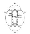
- FIG. 29 shows an example of the installation position of the imaging unit 12031.
- the imaging unit 12031 includes imaging units 12101, 12102, 12103, 12104, and 12105.
- the imaging units 12101, 12102, 12103, 12104, and 12105 are provided, for example, at the front nose, side mirrors, rear bumper, back door, and upper part of the windshield inside the vehicle cabin of the vehicle 12100.
- the imaging unit 12101 provided at the front nose and the imaging unit 12105 provided at the upper part of the windshield inside the vehicle cabin mainly acquire images of the front of the vehicle 12100.
- the imaging units 12102 and 12103 provided at the side mirrors mainly acquire images of the sides of the vehicle 12100.
- the imaging unit 12104 provided at the rear bumper or back door mainly acquires images of the rear of the vehicle 12100.
- the imaging unit 12105 provided at the upper part of the windshield inside the vehicle cabin is mainly used to detect leading vehicles, pedestrians, obstacles, traffic lights, traffic signs, lanes, etc.
- FIG. 29 shows an example of the imaging ranges of the imaging units 12101 to 12104.
- Imaging range 12111 indicates the imaging range of the imaging unit 12101 provided on the front nose
- imaging ranges 12112 and 12113 indicate the imaging ranges of the imaging units 12102 and 12103 provided on the side mirrors, respectively
- imaging range 12114 indicates the imaging range of the imaging unit 12104 provided on the rear bumper or back door.
- an overhead image of the vehicle 12100 viewed from above is obtained by superimposing the image data captured by the imaging units 12101 to 12104.
- At least one of the imaging units 12101 to 12104 may have a function of acquiring distance information.
- at least one of the imaging units 12101 to 12104 may be a stereo camera consisting of multiple imaging elements, or an imaging element having pixels for phase difference detection.
- the microcomputer 12051 can obtain the distance to each solid object within the imaging ranges 12111 to 12114 and the change in this distance over time (relative speed with respect to the vehicle 12100) based on the distance information obtained from the imaging units 12101 to 12104, and can extract as a preceding vehicle, in particular, the closest solid object on the path of the vehicle 12100 that is traveling in approximately the same direction as the vehicle 12100 at a predetermined speed (e.g., 0 km/h or faster). Furthermore, the microcomputer 12051 can set the inter-vehicle distance that should be maintained in advance in front of the preceding vehicle, and perform automatic braking control (including follow-up stop control) and automatic acceleration control (including follow-up start control). In this way, cooperative control can be performed for the purpose of automatic driving, which runs autonomously without relying on the driver's operation.
- automatic braking control including follow-up stop control
- automatic acceleration control including follow-up start control
- the microcomputer 12051 classifies and extracts three-dimensional object data on three-dimensional objects, such as two-wheeled vehicles, ordinary vehicles, large vehicles, pedestrians, utility poles, and other three-dimensional objects, based on the distance information obtained from the imaging units 12101 to 12104, and can use the data to automatically avoid obstacles.
- the microcomputer 12051 distinguishes obstacles around the vehicle 12100 into obstacles that are visible to the driver of the vehicle 12100 and obstacles that are difficult to see.
- the microcomputer 12051 determines the collision risk, which indicates the risk of collision with each obstacle, and when the collision risk is equal to or exceeds a set value and there is a possibility of a collision, it can provide driving assistance for collision avoidance by outputting an alarm to the driver via the audio speaker 12061 or the display unit 12062, or by performing forced deceleration or avoidance steering via the drive system control unit 12010.
- At least one of the imaging units 12101 to 12104 may be an infrared camera that detects infrared rays.
- the microcomputer 12051 can recognize a pedestrian by determining whether or not a pedestrian is present in the image captured by the imaging units 12101 to 12104. The recognition of such a pedestrian is performed, for example, by a procedure of extracting feature points in the image captured by the imaging units 12101 to 12104 as infrared cameras, and a procedure of performing pattern matching processing on a series of feature points that indicate the contour of an object to determine whether or not it is a pedestrian.
- the audio/image output unit 12052 controls the display unit 12062 to superimpose a rectangular contour line for emphasis on the recognized pedestrian.
- the audio/image output unit 12052 may also control the display unit 12062 to display an icon or the like indicating a pedestrian at a desired position.
- the technology disclosed herein can be applied to the imaging unit 12031 of the configuration described above.
- the imaging device of the above-mentioned embodiment can be applied to the imaging unit 12031.
- the above-described embodiment shows an example for realizing the present technology, and there is a corresponding relationship between the matters in the embodiment and the matters specifying the invention in the claims. Similarly, there is a corresponding relationship between the matters specifying the invention in the claims and the matters in the embodiment of the present technology that have the same name.
- the present technology is not limited to the embodiment, and can be realized by making various modifications to the embodiment without departing from the gist of the technology.
- the effects described in this specification are merely examples and are not limiting, and other effects may also be present.
- the present technology can also be configured as follows. (1) a photoelectric conversion unit; a capacitor having one end connected to the photoelectric conversion unit; a first transistor having one end connected to the capacitor and the other end connected to a first node; a second transistor having one end connected to the first node and the other end connected to a power supply; a control unit that controls driving of the first transistor and the second transistor, The control unit turns on the first transistor and the second transistor during at least a part of a period from a read operation of reading out the pixel voltage of the first node to a shutter operation of the photoelectric conversion unit.
- the capacitor accumulates electric charge that overflows from the photoelectric conversion unit.
- the control unit reads out a signal from the capacitor based on a double data sampling (DDS) drive.
- DDS double data sampling
- the photoelectric conversion unit is A first photoelectric conversion unit; a second photoelectric conversion unit having a lower sensitivity than the first photoelectric conversion unit,
- a photoelectric conversion unit a photoelectric conversion unit; a first transistor having one end connected to the photoelectric conversion unit and the other end connected to a first node; a second transistor having one end connected to the first node and the other end connected to a second node; a third transistor having one end connected to the second node and the other end connected to a power supply; a capacitor connected to the second node; a control unit that controls driving of the first transistor, the second transistor, and the third transistor, The control unit turns on the third transistor during at least a portion of an accumulation period in the photoelectric conversion unit.
- the control unit turns on the first transistor and turns off the second transistor when turning on the third transistor during at least a portion of the accumulation period in the photoelectric conversion unit.
- the gate voltage applied to the second transistor is variable.
- the first transistor has a buried gate.
- Imaging device 101 Optical system 102 Solid-state imaging device 103 Imaging control unit 104 Image processing unit 105 Memory unit 106 Display unit 107 Operation unit 108 Bus 111 Pixel array unit 112 Vertical scanning circuit 113 Column readout circuit 114 Column signal processing unit 115 Horizontal scanning circuit 116 Control circuit PD1, PD2 Photodiode 122 Transfer transistor 123 Reset transistor 124 Amplification transistor 125 Selection transistor 126 Capacitor 127 Pass transistor 128 Switching transistor FD1 to FD3 Floating diffusion 131 Horizontal drive line 132 Vertical signal line
Landscapes
- Engineering & Computer Science (AREA)
- Multimedia (AREA)
- Signal Processing (AREA)
- Solid State Image Pick-Up Elements (AREA)
- Transforming Light Signals Into Electric Signals (AREA)
Abstract
電荷蓄積部に用いられるキャパシタの誘電吸収に起因する画質の低下を抑制する。 撮像装置は、光電変換部と、光電変換部に一端が接続されるキャパシタと、一端が前記キャパシタに接続され、他端が第1ノードに接続される第1トランジスタと、一端が第1ノードに接続され、他端が電源に接続される第2トランジスタと、第1トランジスタおよび第2トランジスタの駆動を制御する制御部とを備え、制御部は、第1ノードの画素電圧を読出す読出し動作から、光電変換部のシャッタ動作までの間の少なくとも一部の期間に、第1トランジスタおよび第2トランジスタをオンする。
Description
本技術は、撮像装置に関する。詳しくは、電荷蓄積部が設けられた撮像装置に関する。
撮像のダイナミックレンジを拡大するため、フォトダイオードからオーバーフローした電荷を蓄積するオーバーフロー蓄積容量が用いられることがある。例えば、第1受光素子と第1電荷蓄積部とを接続する第1スイッチおよび第2受光素子と第2電荷蓄積部とを接続する第2スイッチが設けられた撮像装置が提案されている(例えば、特許文献1参照)。
しかしながら、上述の従来技術では、電荷蓄積部に高誘電体キャパシタが用いられると、高誘電体キャパシタの誘電吸収に起因して残像やリニアリティの悪化を招くおそれがあった。
本技術はこのような状況に鑑みて生み出されたものであり、電荷蓄積部に用いられるキャパシタの誘電吸収に起因する画質の低下を抑制することを目的とする。
本技術は、上述の問題点を解消するためになされたものであり、その第1の側面は、光電変換部と、前記光電変換部に一端が接続されるキャパシタと、一端が前記キャパシタに接続され、他端が第1ノードに接続される第1トランジスタと、一端が前記第1ノードに接続され、他端が電源に接続される第2トランジスタと、前記第1トランジスタおよび前記第2トランジスタの駆動を制御する制御部とを備え、前記制御部は、前記第1ノードの画素電圧を読出す読出し動作から、前記光電変換部のシャッタ動作までの間の少なくとも一部の期間に、前記第1トランジスタおよび前記第2トランジスタをオンする撮像装置である。これにより、光電変換部に電荷が蓄積される蓄積期間の前にキャパシタに電圧がかからないようにキャパシタに印加される電圧が制御されるという作用をもたらす。
また、第1の側面において、前記制御部は、前記光電変換部に電荷が蓄積される蓄積期間の前に前記キャパシタに電圧がかからないように前記キャパシタに印加される電圧を制御してもよい。これにより、光電変換部に電荷が蓄積される蓄積期間の前にキャパシタに電荷が蓄積されないように制御されるという作用をもたらす。
また、第1の側面において、前記キャパシタは、高誘電体キャパシタでもよい。これにより、キャパシタのサイズを増大させることなく、キャパシタの容量が増大されるという作用をもたらす。
また、第1の側面において、前記キャパシタは、前記光電変換部からオーバーフローした電荷を蓄積してもよい。これにより、撮像のダイナミックレンジが拡大されるという作用をもたらす。
また、第1の側面において、前記制御部は、DDS(Double Data Sampling)駆動に基づいて、前記キャパシタから信号を読出してもよい。これにより、光電変換部からオーバーフローした電荷が読出されるという作用をもたらす。
また、第1の側面において、前記キャパシタの他端は制御電源に接続され、蓄積期間において、前記制御電源の電位は、前記電源の電位よりも低い中間電位に設定されてもよい。これにより、蓄積期間においてキャパシタの暗電流が低減されるという作用をもたらす。
また、第1の側面において、前記光電変換部は、第1光電変換部と、前記第1光電変換部より感度が低い第2光電変換部とを備え、前記キャパシタは、前記第2光電変換部からオーバーフローした電荷を蓄積してもよい。これにより、撮像のダイナミックレンジが拡大されるという作用をもたらす。
また、第1の側面において、前記キャパシタは、3次元MIM(Metal Insulation Metal)構造を備えてもよい。これにより、キャパシタの平面サイズを増大させることなく、キャパシタの容量が増大されるという作用をもたらす。
また、第1の側面において、前記制御部は、前記第1ノードの画素電圧を読出す読出し動作から、前記光電変換部のシャッタ動作までの間の全期間において、前記第1トランジスタおよび前記第2トランジスタをオンしてもよい。これにより、光電変換部に電荷が蓄積される蓄積期間の前にキャパシタに蓄積される電荷が排出されるという作用をもたらす。
また、第1の側面において、前記制御部は、前記第1ノードの画素電圧を読出す読出し動作から、前記光電変換部のシャッタ動作までの間の期間の途中から、前記第1トランジスタおよび前記第2トランジスタをオンしてもよい。これにより、キャパシタに接続されるフローティングディフュージョンに高電圧がかかる期間を短縮しつつ、光電変換部に電荷が蓄積される蓄積期間の前にキャパシタに蓄積される電荷が排出されるという作用をもたらす。
また、第1の側面において、前記制御部は、前記第1ノードの画素電圧を読出す読出し動作から、前記光電変換部のシャッタ動作までの間の期間において、前記第1トランジスタおよび前記第2トランジスタを間欠的にオンしてもよい。これにより、シャッタ段差の抑制を可能としつつ、光電変換部に電荷が蓄積される蓄積期間の前にキャパシタに蓄積される電荷が排出されるという作用をもたらす。
また、第2の側面は、光電変換部と、一端が前記光電変換部に接続され、他端が第1ノードに接続される第1トランジスタと、一端が前記第1ノードに接続され、他端が第2ノードに接続される第2トランジスタと、一端が前記第2ノードに接続され、他端が電源に接続される第3トランジスタと、前記第2ノードに接続されるキャパシタと、前記第1トランジスタ、前記第2トランジスタおよび前記第3トランジスタの駆動を制御する制御部とを備え、前記制御部は、前記光電変換部での蓄積期間の少なくとも一部の期間に、前記第3トランジスタをオンする撮像装置である。これにより、光電変換部に電荷が蓄積される蓄積期間にキャパシタがリセットされるという作用をもたらす。
また、第2の側面において、前記制御部は、前記光電変換部での蓄積期間の少なくとも一部の期間に前記第3トランジスタをオンするときに、前記第1トランジスタをオンし、前記第2トランジスタをオフしてもよい。これにより、蓄積期間に蓄積可能なフローティングディフュージョンの容量を増大させつつ、蓄積期間にキャパシタがリセットされるという作用をもたらす。
また、第2の側面において、前記キャパシタは、高誘電体キャパシタでもよい。これにより、キャパシタのサイズを増大させることなく、キャパシタの容量が増大されるという作用をもたらす。
また、第2の側面において、前記第2トランジスタに印加されるゲート電圧は可変でもよい。これにより、蓄積期間に蓄積可能なフローティングディフュージョンの容量を増大させつつ、蓄積期間にキャパシタがリセットされるという作用をもたらす。
また、第2の側面において、前記第1ノードに接続され、誘電吸収の影響がないキャパシタをさらに備えてもよい。これにより、第1ノードの容量を増大させつつ、蓄積期間にキャパシタがリセットされるという作用をもたらす。
また、第2の側面において、前記第1トランジスタは、埋め込みゲートを備えてもよい。これにより、第1トランジスタのゲート容量を増大させつつ、蓄積期間にキャパシタがリセットされるという作用をもたらす。
以下、本技術を実施するための形態(以下、実施の形態と称する)について説明する。説明は以下の順序により行う。
1.第1の実施の形態(感度が互いに異なるフォトダイオードが設けられた画素において、読出し動作からシャッタ動作までの間の全期間にリセットトランジスタおよびパストランジスタをオンする例)
2.第2の実施の形態(感度が互いに異なるフォトダイオードが設けられた画素において、読出し動作からシャッタ動作までの期間の途中から、リセットトランジスタおよびパストランジスタをオンする例)
3.第3の実施の形態(感度が互いに異なるフォトダイオードが設けられた画素において、読出し動作からシャッタ動作までの期間にリセットトランジスタおよびパストランジスタを間欠的にオンする例)
4.第4の実施の形態(感度が互いに異なるフォトダイオードが設けられ、各フォトダイオードに転送トランジスタがそれぞれ接続された画素において、読出し動作からシャッタ動作までの間の期間にリセットトランジスタおよびパストランジスタをオンする例)
5.第5の実施の形態(フォトダイオードおよび横型オーバーフロー蓄積容量(LOFIC:Lateral Overflow Integration Capacitor)が設けられた画素において、読出し動作からシャッタ動作までの間の期間にリセットトランジスタおよびパストランジスタをオンする例)
6.第6の実施の形態(フォトダイオードと横型オーバーフロー蓄積容量との間にオーバーフロー制御トランジスタが設けられた画素において、読出し動作からシャッタ動作までの間の期間において、リセットトランジスタおよびパストランジスタをオンする例)
7.第7の実施の形態(蓄積期間中にキャパシタをリセットする例)
8.第8の実施の形態(蓄積期間中にパストランジスタのゲート電圧を可変とする例)
9.第9の実施の形態(誘電吸収の影響がないキャパシタを追加した例)
10.第10の実施の形態(切替トランジスタに埋め込みゲートを設けた例)
11.第11の実施の形態(画素アレイ部を積層した例)
12.移動体への応用例
1.第1の実施の形態(感度が互いに異なるフォトダイオードが設けられた画素において、読出し動作からシャッタ動作までの間の全期間にリセットトランジスタおよびパストランジスタをオンする例)
2.第2の実施の形態(感度が互いに異なるフォトダイオードが設けられた画素において、読出し動作からシャッタ動作までの期間の途中から、リセットトランジスタおよびパストランジスタをオンする例)
3.第3の実施の形態(感度が互いに異なるフォトダイオードが設けられた画素において、読出し動作からシャッタ動作までの期間にリセットトランジスタおよびパストランジスタを間欠的にオンする例)
4.第4の実施の形態(感度が互いに異なるフォトダイオードが設けられ、各フォトダイオードに転送トランジスタがそれぞれ接続された画素において、読出し動作からシャッタ動作までの間の期間にリセットトランジスタおよびパストランジスタをオンする例)
5.第5の実施の形態(フォトダイオードおよび横型オーバーフロー蓄積容量(LOFIC:Lateral Overflow Integration Capacitor)が設けられた画素において、読出し動作からシャッタ動作までの間の期間にリセットトランジスタおよびパストランジスタをオンする例)
6.第6の実施の形態(フォトダイオードと横型オーバーフロー蓄積容量との間にオーバーフロー制御トランジスタが設けられた画素において、読出し動作からシャッタ動作までの間の期間において、リセットトランジスタおよびパストランジスタをオンする例)
7.第7の実施の形態(蓄積期間中にキャパシタをリセットする例)
8.第8の実施の形態(蓄積期間中にパストランジスタのゲート電圧を可変とする例)
9.第9の実施の形態(誘電吸収の影響がないキャパシタを追加した例)
10.第10の実施の形態(切替トランジスタに埋め込みゲートを設けた例)
11.第11の実施の形態(画素アレイ部を積層した例)
12.移動体への応用例
<1.第1の実施の形態>
図1は、第1の実施の形態に係る撮像装置の構成例を示す図である。
図1は、第1の実施の形態に係る撮像装置の構成例を示す図である。
同図において、撮像装置100は、光学系101、固体撮像装置102、撮像制御部103、画像処理部104、記憶部105、表示部106および操作部107を備える。撮像制御部103、画像処理部104、記憶部105、表示部106および操作部107は、バス108を介して互いに接続されている。なお、撮像装置100は、単体としても用いられてもよいし、スマートフォンなどの携帯端末に組み込まれてもよいし、認証装置や監視装置に組み込まれてもよいし、認証装置や監視装置に組み込まれてもよいし、車両やドローンに組み込まれてもよい。
光学系101は、被写体からの光を固体撮像装置102に入射させ、光学像を固体撮像装置102の受光面に結像させる。光学系101は、例えば、フォーカスレンズ、ズームレンズおよび絞りなどを備えることができる。光学系101は、広角レンズ、標準レンズおよび望遠レンズなどの複数のレンズを備えてもよい。
固体撮像装置102は、受光面に結像された光学像を画素ごとに電気信号に変換し、その電気信号をデジタル化して出力する。固体撮像装置102は、例えば、CMOS(Complementary Metal Oxide Semiconductor)イメージセンサである。CMOSイメージセンサは、裏面照射型イメージセンサでもよいし、表面照射型イメージセンサでもよい。なお、本技術の適用においては、固体撮像装置102に限定されず、ToF(Time of Flight)センサやイベント検出センサ等の光検出装置に適用されても良い。
撮像制御部103は、操作部107からの指令に基づいて固体撮像装置102による撮像を制御する。このとき、撮像制御部103は、固体撮像装置102の露光時間、露光量および撮像タイミングなどを制御することができる。
画像処理部104は、固体撮像装置102からの出力に基づいて画像処理を実施する。画像処理は、例えば、ガンマ補正、ホワイトバランス処理、シャープネス処理、階調変換処理である。画像処理部104は、ソフトウェアに基づいて処理を実行するプロセッサを備えてもよい。
記憶部105は、固体撮像装置102で撮像された撮像画像を記憶したり、固体撮像装置102の撮像パラメータなどを記憶したりする。また、記憶部105は、ソフトウェアに基づいて撮像装置100を動作させるプログラムを記憶することができる。記憶部105は、ROM(Read Only Memory)、RAM(Random Access Memory)およびメモリカードを含んでもよい。
表示部106は、撮像画像を表示したり、撮像操作をサポートする各種情報を表示したりする。表示部106は、液晶ディスプレイでもよいし、有機EL(Electro Luminescence)ディスプレイでもよい。
操作部107は、撮像装置100を操作するユーザインターフェースを提供する。操作部107は、例えば、撮像装置100に設けられたボタン、ダイヤルおよびスイッチを含んでもよい。操作部107は、表示部106とともにタッチパネルで構成してもよい。
なお、撮像装置100の形態によっては、上述の機能の一部がなくてよいし、逆に開示していない機能をさらに有してもよい。
図2は、第1の実施の形態に係る固体撮像装置の構成例を示すブロック図である。
同図において、固体撮像装置102は、画素アレイ部111、垂直走査回路112、カラム読出し回路113、カラム信号処理部114、水平走査回路115および制御回路116を備える。
画素アレイ部111は、複数の画素120を備える。画素120は、ロウ方向(水平方向とも言う)およびカラム方向(垂直方向とも言う)に沿ってマトリックス状に配列される。各画素120は、フォトダイオードからオーバーフローした電荷を蓄積するキャパシタを備える。このキャパシタは、横型オーバーフロー蓄積容量でもよい。各画素120は、互いに感度が異なる複数のフォトダイオードを備えてもよい。また、各画素120は、信号の読出し時にカラム読出し回路113との間でソースフォロワを構成することができる。各画素120は、ロウごとに水平駆動線131に接続され、カラムごとに垂直信号線132に接続される。水平駆動線131は、各画素120からの信号の読出し時に各画素120をロウごとに駆動する。垂直信号線132は、画素120からの信号読出し時に流れる電流に基づく電位をカラムごとにカラム信号処理部114に伝送する。
垂直走査回路112は、読出し対象となる画素120をカラム方向に走査する。垂直走査回路112は、垂直レジスタを用いて構成してもよい。
カラム読出し回路113は、各画素120からの信号の読出し時に、各画素120との間でソースフォロワを構成することができる。このとき、カラム読出し回路113は、画素120に保持された電荷に基づいて垂直信号線132の電位を変化させることができる。
カラム信号処理部114は、各画素120からカラム方向に伝送された信号を処理する。例えば、カラム信号処理部114は、各画素120からカラム方向に伝送された信号に基づいて、相関二重サンプリング(CDS:Correlated Double Sampling)処理を実施することができる。また、カラム信号処理部114は、各画素120からカラム方向に伝送された信号に基づいて、AD(Analog to Digital)変換処理を実施し、撮像信号Goutを出力することができる。
カラム信号処理部114は、カラムADC部114Aを備える。カラムADC部114Aは、AD変換処理をカラムごとに並列に実施することができる。このとき、カラムADC部114Aは、画素120から読出された画素信号と参照信号との比較結果に基づいてカラムごとにAD変換することができる。
水平走査回路115は、読出し対象となる画素120をロウ方向に走査する。水平走査回路115は、水平レジスタを用いて構成してもよい。
制御回路116は、垂直走査回路112、カラム読出し回路113、カラム信号処理部114および水平走査回路115を制御する。例えば、制御回路116は、カラム方向の走査タイミング、ロウ方向の走査タイミング、カラム読出し回路113の動作タイミングおよびカラム信号処理部114の処理タイミングを制御することができる。
また、制御回路116は、各画素120のフォトダイオードに電荷が蓄積される蓄積期間の前の蓄積前期間に各画素120のキャパシタに電圧がかからないようにキャパシタに印加される電圧を制御することができる。蓄積前期間は、画素120から画素電圧を読出す読出し動作からシャッタ動作までの間の少なくとも一部の期間に設定することができる。なお、制御回路116は、特許請求の範囲に記載の制御部の一例である。
図3は、第1の実施の形態に係る固体撮像装置に設けられた画素の回路構成例を示す図である。
図3において、画素120は、フォトダイオードPD1、PD2、転送トランジスタ122、リセットトランジスタ123、増幅トランジスタ124、選択トランジスタ125およびフローティングディフュージョンFD1からFD3を備える。さらに、画素120は、キャパシタ126、パストランジスタ127および切替トランジスタ128を備える。転送トランジスタ122、リセットトランジスタ123、増幅トランジスタ124、選択トランジスタ125、パストランジスタ127および切替トランジスタ128は、MOS(Metal Oxide Semiconductor)トランジスタでもよい。キャパシタ126は、MIM(Metal Insulation Metal)容量を用いることができる。キャパシタ126は、3次元MIM容量でもよい。なお、パストランジスタ127は、特許請求の範囲に記載の第1トランジスタの一例である。リセットトランジスタ123は、特許請求の範囲に記載の第2トランジスタの一例である。
また、画素120には、ノードN1からN3が設けられる。各ノードN1からN3には、フローティングディフュージョンFD1からFD3がそれぞれ形成される。
フォトダイオードPD1、PD2は、光電変換を実施し、光電変換した電荷を蓄積する。フォトダイオードPD1、PD2は、互いに感度が異なる。このとき、フォトダイオードPD2の感度は、フォトダイオードPD1の感度よりも小さくすることができる。フォトダイオードPD2の感度をフォトダイオードPD1の感度よりも小さくするために、フォトダイオードPD2の平面サイズをフォトダイオードPD1の平面サイズよりも小さくすることができる。なお、フォトダイオードPD1、PD2は、特許請求の範囲に記載の光電変換部の一例である。
キャパシタ126は、フォトダイオードPD2からオーバーフローした電荷を蓄積する。キャパシタ126は遮光されてもよい。キャパシタ126の一端は、制御電源電圧MVDDに接続され、キャパシタ126の他端は、ノードN3に接続される。また、ノードN3には、フォトダイオードPD2のカソードが接続される。キャパシタ126は、比誘電率が所定値(例:100)よりも高い高誘電体キャパシタでもよい。
転送トランジスタ122は、フォトダイオードPD1に蓄積された電荷をフローティングディフュージョンFD1に転送する。リセットトランジスタ123は、フローティングディフュージョンFD1からFD3をリセットする。増幅トランジスタ124は、フローティングディフュージョンFD1からFD3の電位に応じた信号を出力する。選択トランジスタ125は、増幅トランジスタ124の出力を選択する。パストランジスタ127は、キャパシタ126に蓄積された電荷がフローティングディフュージョンFD1に転送されるパスを設定する。切替トランジスタ128は、増幅トランジスタ124における変換効率を切り替える。
転送トランジスタ122は、フォトダイオードPD1のカソードとノードN1との間に接続される。増幅トランジスタ124と選択トランジスタ125とは、直列に接続されている。増幅トランジスタ124のドレインは、電源電圧VDDに接続されている。増幅トランジスタ124のゲートは、ノードN1に接続されている。選択トランジスタ125のソースは、垂直信号線132に接続されている。
パストランジスタ127は、ノードN2、N3間に接続されている。切替トランジスタ128は、ノードN1、N2間に接続されている。リセットトランジスタ123は、ノードN2と電源電圧VDDとの間に接続されている。このとき、リセットトランジスタ123と切替トランジスタ128とは、直列に接続される。
転送トランジスタ122のゲートには、転送信号TGLが印加される。リセットトランジスタ123のゲートには、リセット信号RSTが印加される。選択トランジスタ125のゲートには、選択信号SELが印加される。パストランジスタ127のゲートには、パス設定信号FCGが印加される。切替トランジスタ128のゲートには、切替信号FDGが印加される。転送信号TGL、リセット信号RST、選択信号SEL、パス設定信号FCGおよび切替信号FDGは、図2の水平駆動線131を介して各画素120に伝送することができる。
ここで、蓄積前期間では、キャパシタ126に電圧がかからないようにキャパシタ126に印加される電圧が制御される。このとき、同図におけるaに示すように、画素120から画素電圧を読出す読出し動作からシャッタ動作までの間の少なくとも一部の期間に、リセット信号RSTおよびパス設定信号FCGが立ち上がり、リセットトランジスタ123およびパストランジスタ127はオンする。このとき、キャパシタ126は、リセットトランジスタ123およびパストランジスタ127を介して、電源電圧VDDに接続される(R1A)。また、制御電源電圧MVDDは、電源電圧VDDに設定することができる。これにより、蓄積前期間において、キャパシタ126の両端に電源電圧VDDが印加され、キャパシタ126に電圧がかからないようにキャパシタ126に印加される電圧が制御される。このため、蓄積期間の開始前にキャパシタ126に電荷が蓄積されないようにすることができ、キャパシタ126の誘電吸収に起因するノードN3の電位変動を抑制することができる。なお、トランジスタをオンするとは、トランジスタの端子に印加される電圧によってトランジスタの閾値電圧を超える状態を表す。また、トランジスタをオフするとは、トランジスタの端子に印加される電圧によってトランジスタの閾値電圧を超えない状態を表し、トランジスタがオフの状態であってもリーク電流の伝導は許容されうる。
蓄積期間では、キャパシタ126がフローティング状態に設定される。このとき、同図におけるbに示すように、シャッタ動作後にパス設定信号FCGが立ち下がり、パストランジスタ127はオフする。このとき、キャパシタ126は、電源電圧VDDから切り離され、フローティング状態に移行される。キャパシタ126がフローティング状態に移行されると、フォトダイオードPD2からオーバーフローした電荷がキャパシタ126に蓄積される(R1B)。
図4は、第1の実施の形態に係る固体撮像装置に適用されるキャパシタ構成例を示す断面図である。なお、以下の説明に用いる図面は、各構成を分かり易くするため、実際の構造と縮尺および形状などを異ならせることがある。
同図において、層間絶縁層151には、配線層161が埋め込まれている。配線層161上には、パッシベーション層152が積層され、パッシベーション層152上には、層間絶縁層153が積層されている。
パッシベーション層152および層間絶縁層153には、配線層161を露出させる開口部KAが形成されている。層間絶縁層153上には、開口部KAの底面および側面が覆われるように容量電極154が形成される。容量電極154上には、容量電極154の底面および側面が覆われるように誘電体層155が形成される。誘電体層155上には、誘電体層155の底面および側面が覆われるように容量電極156が形成される。容量電極154、156および誘電体層155は、キャパシタ126として用いることができる。このとき、キャパシタ126は、3次元MIMを構成することができる。誘電体層155上には、容量電極156が覆われるようにパッシベーション層157が形成される。パッシベーション層157上には、層間絶縁層158が積層されている。層間絶縁層158には、配線層162が埋め込まれる。配線層162は、ビア163を介して容量電極156に接続される。
配線層161、162、ビア163および容量電極154、156の材料は、例えば、Cu、Ti、Ta、Al、W、Ni、Ru、Co、TiN、TaN、WNを用いることができ、複数の材料の積層構造でもよい。
誘電体層155の材料は、例えば、SiO2、SiON、Si3N4、酸化ハフニウム(HfO2)、酸化アルミニウム(Al2O3)、酸化ジルコニウム(ZrO)、酸化タンタル(Ta2O5)、酸化チタン(TiO2)、酸化ランタン(LaO3)、酸化イットリウム(Y2O3)、窒化アルミニウム(AlN)、酸窒化ハフニウム(HfON)、酸窒化アルミニウム(AlON))を用いることができ、複数の材料の積層構造でもよい。
層間絶縁層151、158の材料は、例えば、SiO2、SiON、SiOC、Si3N4、SiCOなどの無機材料や、ポリイミド、アクリル、シリコーン、エポキシ基を骨格とする有機材料を用いることができ、複数の材料の積層構造でもよい。
パッシベーション層152、157の材料は、ポリイミド、アクリル、シリコーン、エポキシ基を骨格とする有機材料やSiO2、Al2O3、AlN、BNなどのフィラーを含む材料を用いることができる。パッシベーション層152、157は、CVD(Chemical Vapor Deposition)膜でもよいし、スパッタ膜でもよい。
図5は、第1の実施の形態に係る固体撮像装置の読出し動作とシャッタ動作との関係の一例を示すタイミングチャートである。
同図において、固体撮像装置は、フレームF1ごとにシャッタ動作SHが繰り返される。このとき、固体撮像装置は、各フレームF1において、シャッタ動作SH間に読出し動作RDを実施する。
ここで、各フレームF1のシャッタ動作SHから読出し動作RDまでの期間に蓄積期間P2が設定される。また、読出し動作RDから次のフレームF1のシャッタ動作SHまでの期間に蓄積前期間P1が設定される。
蓄積前期間P1では、キャパシタ126に電圧がかからないようにキャパシタ126に印加される電圧が制御される。図3におけるaに示すように、読出し動作RDからシャッタ動作SHまでの間の少なくとも一部の期間に、リセットトランジスタ123およびパストランジスタ127はオンする。
蓄積期間P2では、キャパシタ126がフローティング状態に設定される。このとき、図3におけるbに示すように、パストランジスタ127はオフする。
図6は、第1の実施の形態に係る固体撮像装置の読出し動作とシャッタ動作と蓄積動作における各部の波形の一例を示すタイミングチャートである。
同図において、蓄積前期間K19の後、シャッタ期間K11に移行する。シャッタ期間K11では、制御電源電圧MVDDは電源電圧VDDに設定される。選択信号SELは、ロウレベルに設定される。切替信号FDG、リセット信号RSTおよびパス設定信号FCGは、ハイレベルに設定される。そして、転送信号TGLが立ち上がり、フォトダイオード121およびフローティングディフュージョンFD1からFD3の電荷が排出されるとともに、増幅トランジスタ124における変換効率が低下される。そして、転送信号TGLおよびパス設定信号FCGが立ち下がった後、蓄積期間K12に移行する。
蓄積期間K12では、各フォトダイオードPD1、PD2への光の入射に基づいて、各フォトダイオードPD1、PD2に電荷が蓄積される。フォトダイオードPD2からオーバーフローした電荷は、キャパシタ126に蓄積される。ここで、蓄積期間K12では、制御電源電圧MVDDが立ち下がり、中間電位に設定される。中間電位は、電源電圧VDDより低い電圧に設定することができる。ここで、蓄積期間K12では、制御電源電圧MVDDを中間電位に設定することにより、キャパシタ126の暗電流を低減することができる。
次に、低効率P相単体読出し期間K13では、リセット信号RSTが立ち下がるとともに、選択信号SELが立ち上がる。このとき、リセットトランジスタ123がオフするとともに、選択トランジスタ125がオンし、フローティングディフュージョンFD1の低効率P相レベルが増幅トランジスタ124のゲートに印加された時のソースフォロワ動作に基づいて垂直信号線132の電位が設定される。そして、その時の垂直信号線132の電位に基づいて、低効率P相レベルがAD変換される。
次に、高効率P相単体読出し期間K14では、切替信号FDGが立ち下がり、増幅トランジスタ124における変換効率が上昇される。そして、フローティングディフュージョンFD1の高効率P相レベルが増幅トランジスタ124のゲートに印加された時のソースフォロワ動作に基づいて垂直信号線132の電位が設定される。そして、その時の垂直信号線132の電位に基づいて、高効率P相レベルがAD変換される。
その後、選択信号SELが立ち下がるとともに、転送信号TGLが立ち上がる。このとき、選択トランジスタ125がオフするとともに、転送トランジスタ122がオンし、フォトダイオードPD1に蓄積されていた電荷がフローティングディフュージョンFD1に転送される。
次に、高効率D相単体読出し期間K15では、選択信号SELが立ち上がるとともに、転送信号TGLが立ち下がる。このとき、選択トランジスタ125がオンするとともに、転送トランジスタ122がオフし、フローティングディフュージョンFD1の高効率D相レベルが増幅トランジスタ124のゲートに印加された時のソースフォロワ動作に基づいて垂直信号線132の電位が設定される。そして、その時の垂直信号線132の電位に基づいて、高効率D相レベルがAD変換される。
そして、切替信号FDGが立ち上がり、増幅トランジスタ124における変換効率が低下される。さらに、選択信号SELが立ち下がるとともに、転送信号TGLが立ち上がる。このとき、選択トランジスタ125がオフするとともに、転送トランジスタ122がオンし、フォトダイオードPD1に蓄積されていた電荷がフローティングディフュージョンFD1に転送される。
次に、低効率D相単体読出し期間K16では、選択信号SELが立ち上がるとともに、転送信号TGLが立ち下がる。このとき、選択トランジスタ125がオンするとともに、転送トランジスタ122がオフし、フローティングディフュージョンFD1の低効率D相レベルが増幅トランジスタ124のゲートに印加された時のソースフォロワ動作に基づいて垂直信号線132の電位が設定される。そして、その時の垂直信号線132の電位に基づいて、低効率D相レベルがAD変換される。
その後、リセット信号RSTが立ち上がる。このとき、リセットトランジスタ123がオンし、フローティングディフュージョンFD1、FD2の電荷が排出される。
低効率P相単体読出し期間K13、高効率P相単体読出し期間K14、高効率D相単体読出し期間K15および低効率D相単体読出し期間K16では、CDS読出しRDAを実施することができる。
次に、D相一括読出し期間K17では、リセット信号RSTが立ち下がるとともに、パス設定信号FCGが立ち上がる。このとき、リセットトランジスタ123がオフするとともに、パストランジスタ127はオンし、フローティングディフュージョンFD3のD相レベルが増幅トランジスタ124のゲートに印加された時のソースフォロワ動作に基づいて垂直信号線132の電位が設定される。そして、その時の垂直信号線132の電位に基づいて、そのD相レベルがAD変換される。
その後、選択信号SELが立ち下がるとともに、リセット信号RSTが立ち上がる。このとき、選択トランジスタ125がオフするとともに、リセットトランジスタ123がオンし、フローティングディフュージョンFD1からFD3の電荷が排出される。
次に、P相一括読出し期間K18では、リセット信号RSTが立ち下がるとともに、選択信号SELが立ち上がる。このとき、リセットトランジスタ123がオフするとともに、選択トランジスタ125がオンし、フローティングディフュージョンFD3のP相レベルが増幅トランジスタ124のゲートに印加された時のソースフォロワ動作に基づいて垂直信号線132の電位が設定される。そして、その時の垂直信号線132の電位に基づいて、そのP相レベルがAD変換される。P相一括読出し期間K18の後、蓄積前期間K19に移行する。
D相一括読出し期間K17およびP相一括読出し期間K18では、DDS読出しRDBを実施することができる。
蓄積前期間K19では、キャパシタ126に電圧がかからないようにキャパシタ126に印加される電圧が制御される。このとき、パス設定信号FCGが立ち上がった状態でリセット信号RSTが立ち上がる。制御電源電圧MVDDは、電源電圧VDDに維持される。このとき、リセットトランジスタ123およびパストランジスタ127はオンし、キャパシタ126の両端には、電源電圧VDDが印加される。これにより、蓄積前期間K19において、キャパシタ126に電圧がかからないようにキャパシタ126に印加される電圧が制御される。
このように、上述の第1の実施の形態では、感度が互いに異なる複数のフォトダイオードPD1、PD2が設けられた画素120において、読出し動作からシャッタ動作までの間の期間にリセットトランジスタ123およびパストランジスタ127をオンする。これにより、蓄積前期間K19において、キャパシタ126に電圧がかからないようにキャパシタ126に印加される電圧を制御することができる。このため、蓄積期間PK11の開始前にキャパシタ126に電荷が蓄積されないようにすることができ、キャパシタ126の誘電吸収に起因する残像やリニアリティの悪化を抑制することができる。
<2.第2の実施の形態>
上述の第1の実施の形態では、感度が互いに異なる複数のフォトダイオードPD1、PD2が設けられた画素120において、読出し動作からシャッタ動作までの間の全期間にリセットトランジスタ123およびパストランジスタ127をオンした。この第2の実施の形態では、感度が互いに異なる複数のフォトダイオードPD1、PD2が設けられた画素120において、読出し動作からシャッタ動作までの期間の途中から、リセットトランジスタ123およびパストランジスタ127をオンする。
上述の第1の実施の形態では、感度が互いに異なる複数のフォトダイオードPD1、PD2が設けられた画素120において、読出し動作からシャッタ動作までの間の全期間にリセットトランジスタ123およびパストランジスタ127をオンした。この第2の実施の形態では、感度が互いに異なる複数のフォトダイオードPD1、PD2が設けられた画素120において、読出し動作からシャッタ動作までの期間の途中から、リセットトランジスタ123およびパストランジスタ127をオンする。
図7は、第2の実施の形態に係る固体撮像装置の読出し動作とシャッタ動作と蓄積動作における各部の波形の一例を示すタイミングチャートである。
同図において、この固体撮像装置では、上述の第1の実施の形態の蓄積前期間K19に代えて、蓄積前期間K29が設けられる。第2の実施の形態の固体撮像装置のそれ以外の動作は、上述の第1の実施の形態の固体撮像装置の動作と同様である。
蓄積前期間K29では、読出し動作からシャッタ動作までの期間の途中から、キャパシタ126に電圧がかからないようにキャパシタ126に印加される電圧が制御される。このとき、蓄積前期間K29が開始されると、制御電源電圧MVDDが立ち下がり、中間電位に設定されるとともに、パス設定信号FCGが立ち下がる。ここで、制御電源電圧MVDDを中間電位に設定することにより、キャパシタ126に印加される電圧を低下させることができ、キャパシタ126の信頼性を向上させることができる。そして、例えば、蓄積前期間K29の後半において、パス設定信号FCGおよびリセット信号RSTが立ち上がる。このとき、制御電源電圧MVDDも立ち上がり、電源電圧VDDに設定される。このとき、リセットトランジスタ123およびパストランジスタ127はオンし、キャパシタ126の両端には、電源電圧VDDが印加される。これにより、蓄積前期間K29の一部において、キャパシタ126に電圧がかからないようにキャパシタ126に印加される電圧が制御される。
このように、上述の第2の実施の形態では、感度が互いに異なる複数のフォトダイオードPD1、PD2が設けられた画素120において、読出し動作からシャッタ動作までの期間の途中から、リセットトランジスタ123およびパストランジスタ127をオンする。これにより、蓄積前期間K29の一部において、キャパシタ126に電圧がかからないようにすることができ、キャパシタ126の信頼性の低下を抑制しつつ、キャパシタ126の誘電吸収に起因する残像やリニアリティの悪化を抑制することができる。
<3.第3の実施の形態>
上述の第1の実施の形態では、感度が互いに異なる複数のフォトダイオードPD1、PD2が設けられた画素120において、読出し動作からシャッタ動作までの間の全期間において、リセットトランジスタ123およびパストランジスタ127をオンした。この第3の実施の形態では、感度が互いに異なる複数のフォトダイオードPD1、PD2が設けられた画素120において、読出し動作からシャッタ動作までの期間にリセットトランジスタ123およびパストランジスタ127を間欠的にオンする。
上述の第1の実施の形態では、感度が互いに異なる複数のフォトダイオードPD1、PD2が設けられた画素120において、読出し動作からシャッタ動作までの間の全期間において、リセットトランジスタ123およびパストランジスタ127をオンした。この第3の実施の形態では、感度が互いに異なる複数のフォトダイオードPD1、PD2が設けられた画素120において、読出し動作からシャッタ動作までの期間にリセットトランジスタ123およびパストランジスタ127を間欠的にオンする。
図8は、第3の実施の形態に係る固体撮像装置の読出し動作とシャッタ動作と蓄積動作における各部の波形の一例を示すタイミングチャートである。
同図において、この固体撮像装置では、上述の第1の実施の形態の蓄積前期間K19に代えて、蓄積前期間K39が設けられる。第3の実施の形態の固体撮像装置のそれ以外の動作は、上述の第1の実施の形態の固体撮像装置の動作と同様である。
蓄積前期間K39では、読出し動作からシャッタ動作までの期間にキャパシタ126に電圧がかからないようにキャパシタ126に印加される電圧が間欠的に制御される。このとき、蓄積前期間K39が開始されると、パス設定信号FCGが立ち下がる。その後、蓄積前期間K39において、パス設定信号FCGおよびリセット信号RSTがパルス状に立ち上がる。蓄積前期間K39におけるパス設定信号FCGおよびリセット信号RSTのパルス状の立ち上げ回数は、1回でもよいし、複数回でもよい。このとき、リセットトランジスタ123およびパストランジスタ127は間欠的にオンし、キャパシタ126の両端には、電源電圧VDDが間欠的に印加される。これにより、蓄積前期間K39の一部において、キャパシタ126に電圧がかからないようにキャパシタ126に印加される電圧が制御される。
このように、上述の第3の実施の形態では、感度が互いに異なる複数のフォトダイオードPD1、PD2が設けられた画素120において、読出し動作からシャッタ動作までの期間にリセットトランジスタ123およびパストランジスタ127を間欠的にオンする。これにより、蓄積前期間K39において、キャパシタ126に間欠的に電圧がかからないようにすることができ、シャッタ段差の抑制を可能としつつ、キャパシタ126の誘電吸収に起因する残像やリニアリティの悪化を抑制することができる。
<4.第4の実施の形態>
上述の第1の実施の形態では、感度が互いに異なる複数のフォトダイオードPD1、PD2が設けられた画素120において、読出し動作からシャッタ動作までの間の期間にリセットトランジスタ123およびパストランジスタ127をオンした。この第4の実施の形態では、感度が互いに異なる複数のフォトダイオードPD1、PD2に転送トランジスタがそれぞれ接続された画素において、読出し動作からシャッタ動作までの期間にリセットトランジスタ123およびパストランジスタ127をオンする。
上述の第1の実施の形態では、感度が互いに異なる複数のフォトダイオードPD1、PD2が設けられた画素120において、読出し動作からシャッタ動作までの間の期間にリセットトランジスタ123およびパストランジスタ127をオンした。この第4の実施の形態では、感度が互いに異なる複数のフォトダイオードPD1、PD2に転送トランジスタがそれぞれ接続された画素において、読出し動作からシャッタ動作までの期間にリセットトランジスタ123およびパストランジスタ127をオンする。
図9は、第4の実施の形態に係る固体撮像装置に設けられた画素の回路構成例を示す図である。
同図において、画素220は、上述の第1の実施の形態の画素120に転送トランジスタ129が追加されている。第4の実施の形態の画素のそれ以外の構成は、上述の第1の実施の形態の画素120の構成と同様である。
転送トランジスタ129は、フォトダイオードPD2のカソードとノードN3との間に接続される。転送トランジスタ129のゲートには、転送信号TGSが印加される。
図10は、第4の実施の形態に係る固体撮像装置の蓄積前期間および蓄積期間のポテンシャルの一例を示す図である。なお、同図におけるaは、蓄積前期間のポテンシャルの一例を示す。同図におけるbは、シャッタ期間のポテンシャルの一例を示す。同図におけるcは、蓄積期間のポテンシャルの一例を示す。
同図におけるaおよびbにおいて、蓄積前期間およびシャッタ期間では、キャパシタ126に電圧がかからないようにキャパシタ126に印加される電圧VCが制御される。ここで、読出し動作からシャッタ動作までの間の少なくとも一部の期間に、リセット信号RSTおよびパス設定信号FCGはハイレベルに設定される。このとき、リセットトランジスタ123およびパストランジスタ127はオンし、キャパシタ126に電荷ELが蓄積されないようにキャパシタ126から電源電圧VDDまでのポテンシャルが設定される。一方、転送信号TGSはロウレベルに設定され、転送トランジスタ129がオフする。このため、フォトダイオードPD2への光の入射に基づいて、フォトダイオードPD2に電荷が蓄積される。
同図におけるcにおいて、蓄積期間では、キャパシタ126がフローティング状態に設定される。このとき、パス設定信号FCGはロウレベルに設定され、パストランジスタ127はオフする。このため、フォトダイオードPD2からオーバーフローした電荷は、キャパシタ126に蓄積される。
図11は、第4の実施の形態に係る固体撮像装置の読出し動作とシャッタ動作と蓄積動作における各部の波形の一例を示すタイミングチャートである。
同図において、この画素220では、上述の第1の実施の形態の読出し動作にP相サブ読出し期間K41およびD相サブ読出し期間K42が追加される。第4の実施の形態の画素220のそれ以外の動作は、上述の第1の実施の形態の画素120の動作と同様である。
この画素220の読出し動作では、低効率D相単体読出し期間K16の終了時に選択信号SELが立ち下がり、選択トランジスタ125がオフする。そして、リセット信号RSTが立ち下がり、パス設定信号FCGが立ち上がった後、P相サブ読出し期間K41に移行する。
P相サブ読出し期間K41では、選択信号SELが立ち上がる。このとき、選択トランジスタ125がオンし、フローティングディフュージョンFD3のP相サブレベルが増幅トランジスタ124のゲートに印加された時のソースフォロワ動作に基づいて垂直信号線132の電位が設定される。そして、その時の垂直信号線132の電位に基づいて、P相サブレベルがAD変換される。
その後、選択信号SELが立ち下がるとともに、転送信号TGSが立ち上がる。このとき、選択トランジスタ125がオフするとともに、転送トランジスタ129がオンし、フォトダイオードPD2に蓄積されていた電荷がフローティングディフュージョンFD3に転送される。
次に、D相サブ読出し期間K42では、選択信号SELが立ち上がるとともに、転送信号TGSが立ち下がる。このとき、選択トランジスタ125がオンするとともに、転送トランジスタ129がオフし、フローティングディフュージョンFD2のD相サブレベルが増幅トランジスタ124のゲートに印加された時のソースフォロワ動作に基づいて垂直信号線132の電位が設定される。そして、その時の垂直信号線132の電位に基づいて、D相サブレベルがAD変換される。D相サブ読出し期間K42の終了後、D相一括読出し期間K17に移行する。
P相サブ読出し期間K41およびD相サブ読出し期間K42では、CDS読出しRDCを実施することができる。
このように、上述の第4の実施の形態では、感度が互いに異なる複数のフォトダイオードPD1、PD2に転送トランジスタ122、129がそれぞれ接続された画素220において、読出し動作からシャッタ動作までの期間にリセットトランジスタ123およびパストランジスタ127をオンする。これにより、蓄積前期間K19にキャパシタ126に電圧がかからないようにしつつ、フォトダイオードPD2から信号を個別に読出すことが可能となる。このため、ダイナミックレンジの拡大を可能としつつ、キャパシタ126の誘電吸収に起因する残像やリニアリティの悪化を抑制することができる。
上述の第4の実施の形態では、上述の第1の実施の形態の蓄積前期間K19の全期間シャッタ動作を例にとったが、上述の第2の実施の形態の部分期間シャッタ動作を適用してもよいし、上述の第3の実施の形態の間欠シャッタ動作を適用してもよい。
<5.第5の実施の形態>
上述の第1の実施の形態では、感度が互いに異なる複数のフォトダイオードPD1、PD2が設けられた画素120において、読出し動作からシャッタ動作までの間の期間にリセットトランジスタ123およびパストランジスタ127をオンした。この第5の実施の形態では、フォトダイオードPD1が設けられた画素120において、読出し動作からシャッタ動作までの期間にリセットトランジスタ123およびパストランジスタ127をオンする。
上述の第1の実施の形態では、感度が互いに異なる複数のフォトダイオードPD1、PD2が設けられた画素120において、読出し動作からシャッタ動作までの間の期間にリセットトランジスタ123およびパストランジスタ127をオンした。この第5の実施の形態では、フォトダイオードPD1が設けられた画素120において、読出し動作からシャッタ動作までの期間にリセットトランジスタ123およびパストランジスタ127をオンする。
図12は、第5の実施の形態に係る固体撮像装置に設けられた画素の回路構成例を示す図である。
同図において、画素320は、上述の第1の実施の形態のフォトダイオードPD2が除去されている。このとき、キャパシタ126は、フォトダイオードPD1からオーバーフローした電荷を蓄積する横型オーバーフロー蓄積容量として動作することができる。第5の実施の形態の画素320のそれ以外の構成は、上述の第1の実施の形態の画素120の構成と同様である。
図13は、第5の実施の形態に係る固体撮像装置の読出し動作とシャッタ動作と蓄積動作における各部の波形の一例を示すタイミングチャートである。
同図において、この画素320では、低効率D相単体読出し期間K16からD相一括読出し期間K17に移行する間においてリセット信号RSTはロウレベルに維持される。このとき、フローティングディフュージョンFD1、FD2の電荷が維持されたままD相一括読出し期間K17に移行する。そして、フローティングディフュージョンFD1からFD3のD相レベルが増幅トランジスタ124のゲートに印加された時のソースフォロワ動作に基づいて垂直信号線132の電位が設定される。そして、その時の垂直信号線132の電位に基づいて、そのD相レベルがAD変換される。第5の実施の形態の画素320のそれ以外の動作は、上述の第1の実施の形態の画素120の動作と同様である。
このように、上述の第5の実施の形態では、フォトダイオードPD1が設けられた画素120において、読出し動作からシャッタ動作までの期間にリセットトランジスタ123およびパストランジスタ127をオンする。これにより、蓄積前期間K19にキャパシタ126に電圧がかからないようにしつつ、フォトダイオードPD1からオーバーフローした電荷を蓄積する横型オーバーフロー蓄積容量としてキャパシタ126を動作させることが可能となる。このため、ダイナミックレンジの拡大を可能としつつ、キャパシタ126の誘電吸収に起因する残像やリニアリティの悪化を抑制することができる。
上述の第5の実施の形態では、上述の第1の実施の形態の蓄積前期間K19の全期間シャッタ動作を例にとったが、上述の第2の実施の形態の部分期間シャッタ動作を適用してもよいし、上述の第3の実施の形態の間欠シャッタ動作を適用してもよい。
<6.第6の実施の形態>
上述の第5の実施の形態では、キャパシタ126は、フォトダイオードPD1からオーバーフローした電荷を蓄積する横型オーバーフロー蓄積容量としてキャパシタ126を動作させる画素320において、読出し動作からシャッタ動作までの間の期間にリセットトランジスタ123およびパストランジスタ127をオンした。この第6の実施の形態では、フォトダイオードPD1と横型オーバーフロー蓄積容量との間にオーバーフロー制御トランジスが設けられた画素において、読出し動作からシャッタ動作までの期間にリセットトランジスタ123およびパストランジスタ127をオンする。
上述の第5の実施の形態では、キャパシタ126は、フォトダイオードPD1からオーバーフローした電荷を蓄積する横型オーバーフロー蓄積容量としてキャパシタ126を動作させる画素320において、読出し動作からシャッタ動作までの間の期間にリセットトランジスタ123およびパストランジスタ127をオンした。この第6の実施の形態では、フォトダイオードPD1と横型オーバーフロー蓄積容量との間にオーバーフロー制御トランジスが設けられた画素において、読出し動作からシャッタ動作までの期間にリセットトランジスタ123およびパストランジスタ127をオンする。
図14は、第6の実施の形態に係る固体撮像装置に設けられた画素の回路構成例を示す図である。
同図において、画素420は、上述の第5の実施の形態の画素320にオーバーフロー制御トランジスタ130が追加されている。第6の実施の形態の画素420のそれ以外の構成は、上述の第1の実施の形態の画素120の構成と同様である。
オーバーフロー制御トランジスタ130は、フォトダイオードPD1とキャパシタ126との間に接続される。オーバーフロー制御トランジスタ130のゲートには、オーバーフロー制御電圧OFGが印加される。オーバーフロー制御電圧OFGは、フォトダイオードPD1からキャパシタ126への電荷のオーバーフローを制御することができる。オーバーフロー制御電圧OFGは固定電圧でもよい。この画素420の読出し動作は、上述の第5の実施の形態の画素320の読出し動作と同様である。
このように、上述の第6の実施の形態では、フォトダイオードPD1とキャパシタ126との間にオーバーフロー制御トランジスタ130が設けられた画素420において、読出し動作からシャッタ動作までの期間にリセットトランジスタ123およびパストランジスタ127をオンする。これにより、蓄積前期間K19にキャパシタ126に電圧がかからないようにしつつ、フォトダイオードPD1からの電荷のオーバーフローを制御することが可能となる。このため、ダイナミックレンジの拡大を可能としつつ、キャパシタ126の誘電吸収に起因する残像やリニアリティの悪化を抑制することができる。
上述の第6の実施の形態では、上述の第1の実施の形態の蓄積前期間K19の全期間シャッタ動作を例にとったが、上述の第2の実施の形態の部分期間シャッタ動作を適用してもよいし、上述の第3の実施の形態の間欠シャッタ動作を適用してもよい。
<7.第7の実施の形態>
上述の第1の実施の形態では、蓄積前期間キャパシタ126をリセットした。この第7の実施の形態では、蓄積期間中にキャパシタ126をリセットする。
上述の第1の実施の形態では、蓄積前期間キャパシタ126をリセットした。この第7の実施の形態では、蓄積期間中にキャパシタ126をリセットする。
図15は、第7の実施の形態に係る固体撮像装置に設けられた画素の回路構成例を示す図である。
同図において、画素520は、上述の第1の実施の形態の画素120からフォトダイオードPD2が除去されている。また、リセットトランジスタ123は、電源電圧VDDとノードN3との間に接続される。第7の実施の形態の画素520のそれ以外の構成は、上述の第1の実施の形態の画素120の構成と同様である。
リセットトランジスタ123を電源電圧VDDとノードN3との間に接続することにより、パストランジスタ127をオンすることなく、キャパシタ126をリセットすることができる。ここで、パストランジスタ127をオフ状態とすることにより、フローティングディフュージョンFD2に蓄積された電荷を排出させることなく、キャパシタ126をリセットすることができる。キャパシタ126をリセットするときは、切替トランジスタ128をオンし、パストランジスタ127の前段の容量を増大させることができる。このため、ダイナミックレンジの低下を抑制しつつ、蓄積期間中にキャパシタ126をリセットすることができる。なお、リセットトランジスタ123は、本開示の一実施形態における第3トランジスタの一例である。
ここで、制御回路116は、切替トランジスタ128、パストランジスタ127およびリセットトランジスタ123の駆動を制御することができる。このとき、制御回路116は、フォトダイオードPD1での蓄積期間の少なくとも一部の期間にリセットトランジスタ123をオンすることができる。また、制御回路116は、フォトダイオードPD1での蓄積期間の少なくとも一部の期間にリセットトランジスタ123をオンするときは、切替トランジスタ128をオンし、パストランジスタ127をオフすることができる。
図16は、第7の実施の形態に係る固体撮像装置の読出し動作とシャッタ動作との関係の一例を示すタイミングチャートである。
同図において、固体撮像装置は、フレームF1ごとにシャッタ動作SHおよびサブシャッタ動作MSHが繰り返される。各フレームF1には、蓄積期間K1および垂直ブランキング期間K2が設けられる。このとき、固体撮像装置は、各フレームF1において、蓄積期間K1中にサブシャッタ動作MSHを実施する。
ここで、各フレームF1のシャッタ動作SHから読出し動作RDまでの期間に蓄積期間K1が設定される。また、読出し動作RDから次のフレームF1のシャッタ動作SHまでの期間に垂直ブランキング期間K2が設定される。
サブシャッタ動作MSHでは、固体撮像装置は、切替トランジスタ128をオン、パストランジスタ127をオフ、リセットトランジスタ123をオンする。このとき、固体撮像装置は、フローティングディフュージョンFD2に蓄積された電荷を排出させることなく、キャパシタ126をリセットすることができる。
図17から図19は、第7の実施の形態に係る固体撮像装置の垂直ブランキング期間および蓄積期間のポテンシャルの第1の例を示す図である。なお、図17から図19では、サブシャッタ動作MSH前に蓄積された信号電荷がパストランジスタ127よりも前段で受けられる最大の電子数FDQ未満の例を示す。
図17におけるaにおいて、垂直ブランキング期間K2では、切替トランジスタ128、パストランジスタ127およびリセットトランジスタ123がオフされる。このとき、ノードN3には、キャパシタ126の誘電吸収に起因する復帰電圧ESが発生する。
次に、図17におけるbに示すように、シャッタ動作SHでは、切替トランジスタ128、パストランジスタ127およびリセットトランジスタ123がオンされる。このとき、ノードN3では、キャパシタ126の誘電吸収に起因する復帰電圧ESがリセットされる。
次に、図17におけるcに示すように、蓄積期間K1では、切替トランジスタ128、パストランジスタ127およびリセットトランジスタ123がオフされる。このとき、フォトダイオードPD1への光の入射に基づいて、フォトダイオードPD1に電荷ELが蓄積される。ノードN3には、キャパシタ126の誘電吸収に起因する復帰電圧ESが発生する。
次に、図18におけるaに示すように、切替トランジスタ128がオンされる。このとき、ノードN1、N2が結合され、ノードN1、N2間の容量が増大される。フォトダイオードPD1から溢れた電荷ELは、ノードN1、N2間に蓄積することができ、ダイナミックレンジを拡大することができる。このとき、パストランジスタ127よりも前段で受けられる電子数FDQは増加する。この電子数FDQはポテンシャルレンジに比例し、変換効率に反比例する。3変換効率であれば、切替トランジスタ128のオンによる昇圧に基づいてポテンシャルレンジが拡大し、さらにゲート容量による変換効率の低下で電子数FDQが増大する。フローティングディフュージョンFD3で受けられる電子数をフローティングディフュージョンFD1、FD2で一時的に保持可能な状態にすることにより、ダイナミックレンジを減少させることなく、蓄積期間中にキャパシタ126をリセットすることができる。ここで、この電子数FDQがAD変換器等の回路側によって規定されるダイナミックレンジ未満に収まる条件では、サブシャッタ動作MSHは蓄積期間K1の任意のタイミングで実施してもよい。
次に、図18におけるbに示すように、サブシャッタ動作MSHでは、パストランジスタ127がオフされたままリセットトランジスタ123がオンされる。このとき、フォトダイオードPD1から溢れた電荷ELをノードN1、N2間に蓄積したまま、ノードN3では、キャパシタ126の誘電吸収に起因する復帰電圧ESがリセットされる。
次に、図18におけるcに示すように、切替トランジスタ128およびリセットトランジスタ123がオフされる。このとき、ノードN1、N2の結合が解消され、フォトダイオードPD1から溢れた電荷ELが各ノードN1、N2に分配される。
次に、図19におけるaに示すように、蓄積期間K1が進行すると、フォトダイオードPD1から溢れた電荷ELが各ノードN1、N2からも溢れてノードN3にも蓄積される。
次に、図19におけるbに示すように、D相読出しでは、切替トランジスタ128およびパストランジスタ127がオンされ、ノードN1からN3が結合される。
図20および図21は、第7の実施の形態に係る固体撮像装置の垂直ブランキング期間および蓄積期間のポテンシャルの第2の例を示す図である。なお、図20および図21では、パストランジスタ127よりも前段で受けられる最大の電子数FDQに対応するダイナミックレンジが、AD変換器等の回路側によって規定されるダイナミックレンジ相当の例を示す。この例においては、任意のタイミングでサブシャッタ動作MSHを実行することが可能である。図22および図23では、一例として、フォトダイオードPD1で発生した電荷がノードN3に流れ込む前にサブシャッタ動作MSHが実行される例を示す。
図20におけるaにおいて、切替トランジスタ128がオンされる。このとき、ノードN1、N2が結合され、ノードN1、N2間の容量が増大される。フォトダイオードPD1から溢れた電荷ELは、ノードN1、N2間に蓄積される。
次に、図20におけるbに示すように、蓄積期間K1が進行すると、サブシャッタ動作MSH前にノードN1、N2間に蓄積された電荷ELがダイナミックレンジ相当に達する。このとき、サブシャッタ動作MSHが実施されると、フォトダイオードPD1から溢れた電荷ELがノードN1、N2間に蓄積されたまま、ノードN3では、キャパシタ126の誘電吸収に起因する復帰電圧がリセットされる。
次に、図20におけるcに示すように、切替トランジスタ128およびリセットトランジスタ123がオフされる。このとき、ノードN1、N2の結合が解消され、ノードN1、N2間に蓄積された電荷ELがノードN3に溢れる。
次に、図21におけるaに示すように、蓄積期間K1が進行すると、ダイナミックレンジ相当を超えてフォトダイオードPD1から溢れた電荷FEが各ノードN1、N2を介してノードN3に蓄積される。
次に、図21におけるbに示すように、D相読出しでは、切替トランジスタ128およびパストランジスタ127がオンされ、ノードN1からN3が結合される。このとき、ダイナミックレンジ相当を超えてノードN3に蓄積された電荷FEは、回路側の検出レンジを超えているため、D相読出しにおいてフルコードに達し、出力に影響しない。このためダイナミックレンジを低減させることなく、残像を抑制することができる。
図22および図23は、第7の実施の形態に係る固体撮像装置の垂直ブランキング期間および蓄積期間のポテンシャルの第3の例を示す図である。なお、図22および図23では、パストランジスタ127よりも前段で受けられる最大の電子数FDQに対応するダイナミックレンジが、AD変換器等の回路側によって規定されるダイナミックレンジを超える例を示す。この例においては、任意のタイミングでサブシャッタ動作MSHを実行することが可能である。図22および図23では、一例として、フォトダイオードPD1で発生した電荷がノードN3に流れ込んだ後にサブシャッタ動作MSHが実行される例を示す。
図22におけるaにおいて、切替トランジスタ128がオンされる。このとき、ノードN1、N2が結合され、ノードN1、N2間の容量が増大される。そして、ダイナミックレンジ相当を超えてフォトダイオードPD1から溢れた電荷FLは、ノードN1、N2を介してノードN3に蓄積される。
次に、図22におけるbに示すように、サブシャッタ動作MSHでは、パストランジスタ127がオフされたままリセットトランジスタ123がオンされる。このとき、フォトダイオードPD1から溢れた電荷ELがノードN1、N2間に蓄積されたまま、ノードN3では、キャパシタ126の誘電吸収に起因する復帰電圧がリセットされる。また、ダイナミックレンジ相当を超えてノードN3に蓄積されていた電荷FLは排出される。
次に、図22におけるcに示すように、切替トランジスタ128およびリセットトランジスタ123がオフされる。このとき、ノードN1、N2の結合が解消され、ノードN1、N2間に蓄積された電荷ELがノードN3に溢れる。
次に、図23におけるaに示すように、蓄積期間K1が進行すると、ダイナミックレンジ相当を超えてフォトダイオードPD1から溢れた電荷FEが各ノードN1、N2を介してノードN3に蓄積される。
次に、図23におけるbに示すように、D相読出しでは、切替トランジスタ128およびパストランジスタ127がオンされ、ノードN1からN3が結合される。このとき、ダイナミックレンジ相当を超えてノードN3に蓄積された電荷FEは、回路側の検出レンジを超えているため、D相読出しにおいてフルコードに達し、出力に影響しない。このためダイナミックレンジを低減させることなく、残像を抑制することができる。
このように、上述の第7の実施の形態では、蓄積期間中に切替トランジスタ128をオン、パストランジスタ127をオフ、リセットトランジスタ123をオンする。これにより、フローティングディフュージョンFD2に蓄積された電荷を排出させることなく、キャパシタ126をリセットすることができる。このため、ダイナミックレンジの低下を抑制しつつ、キャパシタ126の誘電吸収に起因する残像やリニアリティの悪化を抑制することができる。
<8.第8の実施の形態>
上述の第7の実施の形態では、フローティングディフュージョンFD2に蓄積された電荷を排出させることなく、蓄積期間中にキャパシタ126をリセットした。この第8の実施の形態では、蓄積期間中にパストランジスタ127のゲート電圧を可変とする。
上述の第7の実施の形態では、フローティングディフュージョンFD2に蓄積された電荷を排出させることなく、蓄積期間中にキャパシタ126をリセットした。この第8の実施の形態では、蓄積期間中にパストランジスタ127のゲート電圧を可変とする。
図24は、第8の実施の形態に係る固体撮像装置の蓄積期間のポテンシャルの一例を示す図である。
同図におけるaにおいて、パストランジスタ127がオフしているときは、ノードN1、N2間に電荷ELを蓄積させるポテンシャル障壁が形成される。このとき、パストランジスタ127よりも前段で受けられる電子数FDQは、このポテンシャル障壁の高さに依存する。
このため、パストランジスタ127よりも前段で受けられる電子数FDQを増大させるため、パストランジスタ127のゲートの負電圧を可変としてもよい。例えば、同図におけるbに示すように、パストランジスタ127のゲートの負電圧を増大させることにより、ノードN1、N2間に電荷ELを蓄積させるポテンシャル障壁を高くすることができ、パストランジスタ127よりも前段で受けられる電子数FDQを増大させることができる。
このように、上述の第8の実施の形態では、蓄積期間中にパストランジスタ127のゲート電圧を可変とする。これにより、蓄積期間に蓄積可能なフローティングディフュージョンの容量を増大させつつ、蓄積期間にキャパシタ126をリセットすることができる。
<9.第9の実施の形態>
上述の第7の実施の形態では、フローティングディフュージョンFD2に蓄積された電荷を排出させることなく、蓄積期間中にキャパシタ126をリセットした。この第9の実施の形態では、誘電吸収の影響がないキャパシタを追加する。
上述の第7の実施の形態では、フローティングディフュージョンFD2に蓄積された電荷を排出させることなく、蓄積期間中にキャパシタ126をリセットした。この第9の実施の形態では、誘電吸収の影響がないキャパシタを追加する。
図25は、第9の実施の形態に係る固体撮像装置に設けられた画素の回路構成例を示す図である。
同図において、画素620は、上述の第7の実施の形態の画素520にキャパシタ626が追加されている。第9の実施の形態の画素620のそれ以外の構成は、上述の第7の実施の形態の画素520の構成と同様である。
キャパシタ626は、ノードN2と電源電圧VDDとの間に接続される。キャパシタ626は、誘電吸収の影響がないように構成してもよいし、誘電吸収の影響がないようにキャパシタ626からの読出しを制御してもよい。例えば、キャパシタ626は、電極間の絶縁に分極が発生しない材料を用いてもよいし、キャパシタ626からの読出しにCDSを実施してもよい。
このように、上述の第9の実施の形態では、誘電吸収の影響がないキャパシタ626をノードN2に接続する。これにより、蓄積期間中のキャパシタ126のリセット時にパストランジスタ127よりも前段で受けられる電子数FDQを増大させることができ、残像の発生を抑制しつつ、ダイナミックレンジを拡大することができる。
<10.第10の実施の形態>
上述の第7の実施の形態では、フローティングディフュージョンFD2に蓄積された電荷を排出させることなく、蓄積期間中にキャパシタ126をリセットした。この第10の実施の形態では、切替トランジスタに埋め込みゲートを設ける。
上述の第7の実施の形態では、フローティングディフュージョンFD2に蓄積された電荷を排出させることなく、蓄積期間中にキャパシタ126をリセットした。この第10の実施の形態では、切替トランジスタに埋め込みゲートを設ける。
図26は、第10の実施の形態に係る固体撮像装置に設けられた画素の構成例を示す断面図である。
同図において、半導体基板711には、不純物拡散層721から723が互いに分離して形成されている。半導体基板711の材料は、Si、InP、InGaP、InAlP、InGaAs、InAlAsまたはカルコパイライト構造の化合物半導体などを用いることができる。各不純物拡散層721から723は、フローティングディフュージョンFD1からFD3として用いることができる。
半導体基板711上には、不純物拡散層721に端部がかかるようにゲート電極731が形成されている。また、半導体基板711上には、不純物拡散層721、722間に掛け渡されるようにゲート電極732が形成されている。さらに、半導体基板711上には、不純物拡散層722、723間に掛け渡されるようにゲート電極733が形成されている。各ゲート電極731から733と半導体基板711とを絶縁するために、各ゲート電極731から733と半導体基板711との間には、ゲート絶縁膜が形成される。各ゲート電極731から733は、転送トランジスタ122、切替トランジスタ128およびパストランジスタ127にそれぞれ用いることができる。
また、半導体基板711には、埋め込みゲート712が埋め込まれている。埋め込みゲート712は、ゲート電極732に接続される。埋め込みゲート712と半導体基板711とを絶縁するために、埋め込みゲート712と半導体基板711との間には、ゲート絶縁膜が形成される。ここで、ゲート電極732に接続される埋め込みゲート712を設けることにより、切替トランジスタ128のゲート容量を増大させることができる。
このように、上述の第10の実施の形態では、切替トランジスタ128に埋め込みゲート712を設ける。これにより、蓄積期間中のキャパシタ126のリセット時にパストランジスタ127よりも前段で受けられる電子数FDQを増大させることができ、残像の発生を抑制しつつ、ダイナミックレンジを拡大することができる。
<11.第11の実施の形態>
上述の第1の実施の形態では、感度が互いに異なるフォトダイオードPD1、PD2が設けられた画素120において、読出し動作からシャッタ動作までの間の期間においてオンされるリセットトランジスタ123およびパストランジスタ127を設けた。この第11の実施の形態では、画素がマトリックス状に配列された画素アレイ部が設けられた半導体チップを積層化する。
上述の第1の実施の形態では、感度が互いに異なるフォトダイオードPD1、PD2が設けられた画素120において、読出し動作からシャッタ動作までの間の期間においてオンされるリセットトランジスタ123およびパストランジスタ127を設けた。この第11の実施の形態では、画素がマトリックス状に配列された画素アレイ部が設けられた半導体チップを積層化する。
図27は、第11の実施の形態に係る画素アレイ部の積層例を示す斜視図である。
同図において、固体撮像装置は、半導体チップ921、922を備える。半導体チップ922は、半導体チップ921上に積層される。
半導体チップ922には、画素アレイ部923が形成される。画素アレイ部923には、画素931がロウ方向およびカラム方向にマトリックス状に配置される。画素931は、上述の第1から第6の実施の形態のいずれの画素でもよい。画素アレイ部923の周辺には、パッド電極932およびビア電極933が形成される。ビア電極933は、半導体チップ922を貫通し、半導体チップ921、922同士を電気的に接続することができる。
半導体チップ921には、周辺回路924が形成される。周辺回路924には、カラム読出し回路925、カラムADC926、通信インタフェース927および制御回路928が形成される。カラム読出し回路925およびカラムADC926は、画素アレイ部923のカラム方向の両側の位置に対応するように形成してもよい。
制御回路928は、各画素931のフォトダイオードに電荷が蓄積される蓄積期間の前の蓄積前期間に各画素931のキャパシタに電圧がかからないようにキャパシタに印加される電圧を制御することができる。蓄積前期間は、画素931から画素電圧を読出す読出し動作からシャッタ動作までの間の少なくとも一部の期間に設定することができる。
半導体チップ921、922は、直接接合してもよい。半導体チップ921、922の直接接合では、ハイブリッドボンディングを用いることができる。このとき、半導体チップ921、922は、Cu-Cu接続に基づいて電気的に接続してもよい。半導体チップ921、922に用いられる半導体基板の材料は、Siでもよいし、InGaAsでもよいし、InPでもよい。
このように、上述の第11の実施の形態では、画素アレイ部923が形成される半導体チップ922を、周辺回路924が形成される半導体チップ921上に積層する。これにより、固体撮像装置が形成された半導体チップの実装面積の増大を抑制しつつ、固体撮像装置の感度を増大させることが可能となる。
<12.移動体への応用例>
本開示に係る技術(本技術)は、様々な製品へ応用することができる。例えば、本開示に係る技術は、自動車、電気自動車、ハイブリッド電気自動車、自動二輪車、自転車、パーソナルモビリティ、飛行機、ドローン、船舶、ロボット等のいずれかの種類の移動体に搭載される装置として実現されてもよい。
本開示に係る技術(本技術)は、様々な製品へ応用することができる。例えば、本開示に係る技術は、自動車、電気自動車、ハイブリッド電気自動車、自動二輪車、自転車、パーソナルモビリティ、飛行機、ドローン、船舶、ロボット等のいずれかの種類の移動体に搭載される装置として実現されてもよい。
図28は、本開示に係る技術が適用され得る移動体制御システムの一例である車両制御システムの概略的な構成例を示すブロック図である。
車両制御システム12000は、通信ネットワーク12001を介して接続された複数の電子制御ユニットを備える。図28に示した例では、車両制御システム12000は、駆動系制御ユニット12010、ボディ系制御ユニット12020、車外情報検出ユニット12030、車内情報検出ユニット12040、及び統合制御ユニット12050を備える。また、統合制御ユニット12050の機能構成として、マイクロコンピュータ12051、音声画像出力部12052、及び車載ネットワークI/F(interface)12053が図示されている。
駆動系制御ユニット12010は、各種プログラムにしたがって車両の駆動系に関連する装置の動作を制御する。例えば、駆動系制御ユニット12010は、内燃機関又は駆動用モータ等の車両の駆動力を発生させるための駆動力発生装置、駆動力を車輪に伝達するための駆動力伝達機構、車両の舵角を調節するステアリング機構、及び、車両の制動力を発生させる制動装置等の制御装置として機能する。
ボディ系制御ユニット12020は、各種プログラムにしたがって車体に装備された各種装置の動作を制御する。例えば、ボディ系制御ユニット12020は、キーレスエントリシステム、スマートキーシステム、パワーウィンドウ装置、あるいは、ヘッドランプ、バックランプ、ブレーキランプ、ウィンカー又はフォグランプ等の各種ランプの制御装置として機能する。この場合、ボディ系制御ユニット12020には、鍵を代替する携帯機から発信される電波又は各種スイッチの信号が入力され得る。ボディ系制御ユニット12020は、これらの電波又は信号の入力を受け付け、車両のドアロック装置、パワーウィンドウ装置、ランプ等を制御する。
車外情報検出ユニット12030は、車両制御システム12000を搭載した車両の外部の情報を検出する。例えば、車外情報検出ユニット12030には、撮像部12031が接続される。車外情報検出ユニット12030は、撮像部12031に車外の画像を撮像させるとともに、撮像された画像を受信する。車外情報検出ユニット12030は、受信した画像に基づいて、人、車、障害物、標識又は路面上の文字等の物体検出処理又は距離検出処理を行ってもよい。
撮像部12031は、光を受光し、その光の受光量に応じた電気信号を出力する光センサである。撮像部12031は、電気信号を画像として出力することもできるし、測距の情報として出力することもできる。また、撮像部12031が受光する光は、可視光であってもよいし、赤外線等の非可視光であってもよい。
車内情報検出ユニット12040は、車内の情報を検出する。車内情報検出ユニット12040には、例えば、運転者の状態を検出する運転者状態検出部12041が接続される。運転者状態検出部12041は、例えば運転者を撮像するカメラを含み、車内情報検出ユニット12040は、運転者状態検出部12041から入力される検出情報に基づいて、運転者の疲労度合い又は集中度合いを算出してもよいし、運転者が居眠りをしていないかを判別してもよい。
マイクロコンピュータ12051は、車外情報検出ユニット12030又は車内情報検出ユニット12040で取得される車内外の情報に基づいて、駆動力発生装置、ステアリング機構又は制動装置の制御目標値を演算し、駆動系制御ユニット12010に対して制御指令を出力することができる。例えば、マイクロコンピュータ12051は、車両の衝突回避あるいは衝撃緩和、車間距離に基づく追従走行、車速維持走行、車両の衝突警告、又は車両のレーン逸脱警告等を含むADAS(Advanced Driver Assistance System)の機能実現を目的とした協調制御を行うことができる。
また、マイクロコンピュータ12051は、車外情報検出ユニット12030又は車内情報検出ユニット12040で取得される車両の周囲の情報に基づいて駆動力発生装置、ステアリング機構又は制動装置等を制御することにより、運転者の操作に拠らずに自律的に走行する自動運転等を目的とした協調制御を行うことができる。
また、マイクロコンピュータ12051は、車外情報検出ユニット12030で取得される車外の情報に基づいて、ボディ系制御ユニット12020に対して制御指令を出力することができる。例えば、マイクロコンピュータ12051は、車外情報検出ユニット12030で検知した先行車又は対向車の位置に応じてヘッドランプを制御し、ハイビームをロービームに切り替える等の防眩を図ることを目的とした協調制御を行うことができる。
音声画像出力部12052は、車両の搭乗者又は車外に対して、視覚的又は聴覚的に情報を通知することが可能な出力装置へ音声及び画像のうちの少なくとも一方の出力信号を送信する。図28の例では、出力装置として、オーディオスピーカ12061、表示部12062及びインストルメントパネル12063が例示されている。表示部12062は、例えば、オンボードディスプレイ及びヘッドアップディスプレイの少なくとも一つを含んでいてもよい。
図29は、撮像部12031の設置位置の例を示す図である。
図29では、撮像部12031として、撮像部12101,12102,12103,12104,12105を有する。
撮像部12101,12102,12103,12104,12105は、例えば、車両12100のフロントノーズ、サイドミラー、リアバンパ、バックドア及び車室内のフロントガラスの上部等の位置に設けられる。フロントノーズに備えられる撮像部12101及び車室内のフロントガラスの上部に備えられる撮像部12105は、主として車両12100の前方の画像を取得する。サイドミラーに備えられる撮像部12102,12103は、主として車両12100の側方の画像を取得する。リアバンパ又はバックドアに備えられる撮像部12104は、主として車両12100の後方の画像を取得する。車室内のフロントガラスの上部に備えられる撮像部12105は、主として先行車両又は、歩行者、障害物、信号機、交通標識又は車線等の検出に用いられる。
なお、図29には、撮像部12101ないし12104の撮影範囲の一例が示されている。撮像範囲12111は、フロントノーズに設けられた撮像部12101の撮像範囲を示し、撮像範囲12112,12113は、それぞれサイドミラーに設けられた撮像部12102,12103の撮像範囲を示し、撮像範囲12114は、リアバンパ又はバックドアに設けられた撮像部12104の撮像範囲を示す。例えば、撮像部12101ないし12104で撮像された画像データが重ね合わせられることにより、車両12100を上方から見た俯瞰画像が得られる。
撮像部12101ないし12104の少なくとも1つは、距離情報を取得する機能を有していてもよい。例えば、撮像部12101ないし12104の少なくとも1つは、複数の撮像素子からなるステレオカメラであってもよいし、位相差検出用の画素を有する撮像素子であってもよい。
例えば、マイクロコンピュータ12051は、撮像部12101ないし12104から得られた距離情報を基に、撮像範囲12111ないし12114内における各立体物までの距離と、この距離の時間的変化(車両12100に対する相対速度)を求めることにより、特に車両12100の進行路上にある最も近い立体物で、車両12100と略同じ方向に所定の速度(例えば、0km/h以上)で走行する立体物を先行車として抽出することができる。さらに、マイクロコンピュータ12051は、先行車の手前に予め確保すべき車間距離を設定し、自動ブレーキ制御(追従停止制御も含む)や自動加速制御(追従発進制御も含む)等を行うことができる。このように運転者の操作に拠らずに自律的に走行する自動運転等を目的とした協調制御を行うことができる。
例えば、マイクロコンピュータ12051は、撮像部12101ないし12104から得られた距離情報を元に、立体物に関する立体物データを、2輪車、普通車両、大型車両、歩行者、電柱等その他の立体物に分類して抽出し、障害物の自動回避に用いることができる。例えば、マイクロコンピュータ12051は、車両12100の周辺の障害物を、車両12100のドライバが視認可能な障害物と視認困難な障害物とに識別する。そして、マイクロコンピュータ12051は、各障害物との衝突の危険度を示す衝突リスクを判断し、衝突リスクが設定値以上で衝突可能性がある状況であるときには、オーディオスピーカ12061や表示部12062を介してドライバに警報を出力することや、駆動系制御ユニット12010を介して強制減速や回避操舵を行うことで、衝突回避のための運転支援を行うことができる。
撮像部12101ないし12104の少なくとも1つは、赤外線を検出する赤外線カメラであってもよい。例えば、マイクロコンピュータ12051は、撮像部12101ないし12104の撮像画像中に歩行者が存在するか否かを判定することで歩行者を認識することができる。かかる歩行者の認識は、例えば赤外線カメラとしての撮像部12101ないし12104の撮像画像における特徴点を抽出する手順と、物体の輪郭を示す一連の特徴点にパターンマッチング処理を行って歩行者か否かを判別する手順によって行われる。マイクロコンピュータ12051が、撮像部12101ないし12104の撮像画像中に歩行者が存在すると判定し、歩行者を認識すると、音声画像出力部12052は、当該認識された歩行者に強調のための方形輪郭線を重畳表示するように、表示部12062を制御する。また、音声画像出力部12052は、歩行者を示すアイコン等を所望の位置に表示するように表示部12062を制御してもよい。
以上、本開示に係る技術が適用され得る車両制御システムの一例について説明した。本開示に係る技術は、以上説明した構成のうち、撮像部12031に適用され得る。具体的には、例えば、上述の実施の形態の撮像装置は、撮像部12031に適用することができる。車両制御システム12000に本開示に係る技術を適用することにより、ダイナミックレンジの拡大を可能としつつ、撮像時の残像やリニアリティの悪化を抑制することができる。
なお、上述の実施の形態は本技術を具現化するための一例を示したものであり、実施の形態における事項と、特許請求の範囲における発明特定事項とはそれぞれ対応関係を有する。同様に、特許請求の範囲における発明特定事項と、これと同一名称を付した本技術の実施の形態における事項とはそれぞれ対応関係を有する。ただし、本技術は実施の形態に限定されるものではなく、その要旨を逸脱しない範囲において実施の形態に種々の変形を施すことにより具現化することができる。また、本明細書に記載された効果はあくまで例示であって、限定されるものではなく、また、他の効果があってもよい。
なお、本技術は以下のような構成もとることができる。
(1)光電変換部と、
前記光電変換部に一端が接続されるキャパシタと、
一端が前記キャパシタに接続され、他端が第1ノードに接続される第1トランジスタと、
一端が前記第1ノードに接続され、他端が電源に接続される第2トランジスタと、
前記第1トランジスタおよび前記第2トランジスタの駆動を制御する制御部とを備え、
前記制御部は、前記第1ノードの画素電圧を読出す読出し動作から、前記光電変換部のシャッタ動作までの間の少なくとも一部の期間に、前記第1トランジスタおよび前記第2トランジスタをオンする
撮像装置。
(2)前記制御部は、前記光電変換部に電荷が蓄積される蓄積期間の前に前記キャパシタに電圧がかからないように前記キャパシタに印加される電圧を制御する
前記(1)に記載の撮像装置。
(3)前記キャパシタは、高誘電体キャパシタである
前記(1)または(2)に記載の撮像装置。
(4)前記キャパシタは、前記光電変換部からオーバーフローした電荷を蓄積する
前記(1)から(3)のいずれかに記載の撮像装置。
(5)前記制御部は、DDS(Double Data Sampling)駆動に基づいて、前記キャパシタから信号を読出す
前記(1)から(4)のいずれかに記載の撮像装置。
(6)前記キャパシタの他端は制御電源に接続され、蓄積期間において、前記制御電源の電位は、前記電源の電位よりも低い中間電位に設定される
前記(1)から(5)のいずれかに記載の撮像装置。
(7)前記光電変換部は、
第1光電変換部と、
前記第1光電変換部より感度が低い第2光電変換部とを備え、
前記キャパシタは、前記第2光電変換部からオーバーフローした電荷を蓄積する
前記(1)から(6)のいずれかに記載の撮像装置。
(8)前記キャパシタは、3次元MIM(Metal Insulation Metal)構造を備える
前記(1)から(7)のいずれかに記載の撮像装置。
(9)前記制御部は、前記第1ノードの画素電圧を読出す読出し動作から、前記光電変換部のシャッタ動作までの間の全期間において、前記第1トランジスタおよび前記第2トランジスタをオンする
前記(1)から(8)のいずれかに記載の撮像装置。
(10)前記制御部は、前記第1ノードの画素電圧を読出す読出し動作から、前記光電変換部のシャッタ動作までの間の期間の途中から、前記第1トランジスタおよび前記第2トランジスタをオンする
前記(1)から(8)のいずれかに記載の撮像装置。
(11)前記制御部は、前記第1ノードの画素電圧を読出す読出し動作から、前記光電変換部のシャッタ動作までの間の期間において、前記第1トランジスタおよび前記第2トランジスタを間欠的にオンする
前記(1)から(8)のいずれかに記載の撮像装置。
(12)光電変換部と、
一端が前記光電変換部に接続され、他端が第1ノードに接続される第1トランジスタと、
一端が前記第1ノードに接続され、他端が第2ノードに接続される第2トランジスタと、
一端が前記第2ノードに接続され、他端が電源に接続される第3トランジスタと、
前記第2ノードに接続されるキャパシタと、
前記第1トランジスタ、前記第2トランジスタおよび前記第3トランジスタの駆動を制御する制御部とを備え、
前記制御部は、前記光電変換部での蓄積期間の少なくとも一部の期間に、前記第3トランジスタをオンする
撮像装置。
(13)前記制御部は、前記光電変換部での蓄積期間の少なくとも一部の期間に前記第3トランジスタをオンするときに、前記第1トランジスタをオンし、前記第2トランジスタをオフする
前記(12)に記載の撮像装置。
(14)前記キャパシタは、高誘電体キャパシタである
前記(12)または(13)に記載の撮像装置。
(15)前記第2トランジスタに印加されるゲート電圧は可変である
前記(12)から(14)のいずれかに記載の撮像装置。
(16)前記第1ノードに接続され、誘電吸収の影響がないキャパシタ
をさらに備える前記(12)から(15)のいずれかに記載の撮像装置。
(17)前記第1トランジスタは、埋め込みゲート
を備える前記(12)から(16)のいずれかに記載の撮像装置。
(1)光電変換部と、
前記光電変換部に一端が接続されるキャパシタと、
一端が前記キャパシタに接続され、他端が第1ノードに接続される第1トランジスタと、
一端が前記第1ノードに接続され、他端が電源に接続される第2トランジスタと、
前記第1トランジスタおよび前記第2トランジスタの駆動を制御する制御部とを備え、
前記制御部は、前記第1ノードの画素電圧を読出す読出し動作から、前記光電変換部のシャッタ動作までの間の少なくとも一部の期間に、前記第1トランジスタおよび前記第2トランジスタをオンする
撮像装置。
(2)前記制御部は、前記光電変換部に電荷が蓄積される蓄積期間の前に前記キャパシタに電圧がかからないように前記キャパシタに印加される電圧を制御する
前記(1)に記載の撮像装置。
(3)前記キャパシタは、高誘電体キャパシタである
前記(1)または(2)に記載の撮像装置。
(4)前記キャパシタは、前記光電変換部からオーバーフローした電荷を蓄積する
前記(1)から(3)のいずれかに記載の撮像装置。
(5)前記制御部は、DDS(Double Data Sampling)駆動に基づいて、前記キャパシタから信号を読出す
前記(1)から(4)のいずれかに記載の撮像装置。
(6)前記キャパシタの他端は制御電源に接続され、蓄積期間において、前記制御電源の電位は、前記電源の電位よりも低い中間電位に設定される
前記(1)から(5)のいずれかに記載の撮像装置。
(7)前記光電変換部は、
第1光電変換部と、
前記第1光電変換部より感度が低い第2光電変換部とを備え、
前記キャパシタは、前記第2光電変換部からオーバーフローした電荷を蓄積する
前記(1)から(6)のいずれかに記載の撮像装置。
(8)前記キャパシタは、3次元MIM(Metal Insulation Metal)構造を備える
前記(1)から(7)のいずれかに記載の撮像装置。
(9)前記制御部は、前記第1ノードの画素電圧を読出す読出し動作から、前記光電変換部のシャッタ動作までの間の全期間において、前記第1トランジスタおよび前記第2トランジスタをオンする
前記(1)から(8)のいずれかに記載の撮像装置。
(10)前記制御部は、前記第1ノードの画素電圧を読出す読出し動作から、前記光電変換部のシャッタ動作までの間の期間の途中から、前記第1トランジスタおよび前記第2トランジスタをオンする
前記(1)から(8)のいずれかに記載の撮像装置。
(11)前記制御部は、前記第1ノードの画素電圧を読出す読出し動作から、前記光電変換部のシャッタ動作までの間の期間において、前記第1トランジスタおよび前記第2トランジスタを間欠的にオンする
前記(1)から(8)のいずれかに記載の撮像装置。
(12)光電変換部と、
一端が前記光電変換部に接続され、他端が第1ノードに接続される第1トランジスタと、
一端が前記第1ノードに接続され、他端が第2ノードに接続される第2トランジスタと、
一端が前記第2ノードに接続され、他端が電源に接続される第3トランジスタと、
前記第2ノードに接続されるキャパシタと、
前記第1トランジスタ、前記第2トランジスタおよび前記第3トランジスタの駆動を制御する制御部とを備え、
前記制御部は、前記光電変換部での蓄積期間の少なくとも一部の期間に、前記第3トランジスタをオンする
撮像装置。
(13)前記制御部は、前記光電変換部での蓄積期間の少なくとも一部の期間に前記第3トランジスタをオンするときに、前記第1トランジスタをオンし、前記第2トランジスタをオフする
前記(12)に記載の撮像装置。
(14)前記キャパシタは、高誘電体キャパシタである
前記(12)または(13)に記載の撮像装置。
(15)前記第2トランジスタに印加されるゲート電圧は可変である
前記(12)から(14)のいずれかに記載の撮像装置。
(16)前記第1ノードに接続され、誘電吸収の影響がないキャパシタ
をさらに備える前記(12)から(15)のいずれかに記載の撮像装置。
(17)前記第1トランジスタは、埋め込みゲート
を備える前記(12)から(16)のいずれかに記載の撮像装置。
100 撮像装置
101 光学系
102 固体撮像装置
103 撮像制御部
104 画像処理部
105 記憶部
106 表示部
107 操作部
108 バス
111 画素アレイ部
112 垂直走査回路
113 カラム読出し回路
114 カラム信号処理部
115 水平走査回路
116 制御回路
PD1、PD2 フォトダイオード
122 転送トランジスタ
123 リセットトランジスタ
124 増幅トランジスタ
125 選択トランジスタ
126 キャパシタ
127 パストランジスタ
128 切替トランジスタ
FD1からFD3 フローティングディフュージョン
131 水平駆動線
132 垂直信号線
101 光学系
102 固体撮像装置
103 撮像制御部
104 画像処理部
105 記憶部
106 表示部
107 操作部
108 バス
111 画素アレイ部
112 垂直走査回路
113 カラム読出し回路
114 カラム信号処理部
115 水平走査回路
116 制御回路
PD1、PD2 フォトダイオード
122 転送トランジスタ
123 リセットトランジスタ
124 増幅トランジスタ
125 選択トランジスタ
126 キャパシタ
127 パストランジスタ
128 切替トランジスタ
FD1からFD3 フローティングディフュージョン
131 水平駆動線
132 垂直信号線
Claims (17)
- 光電変換部と、
前記光電変換部に一端が接続されるキャパシタと、
一端が前記キャパシタに接続され、他端が第1ノードに接続される第1トランジスタと、
一端が前記第1ノードに接続され、他端が電源に接続される第2トランジスタと、
前記第1トランジスタおよび前記第2トランジスタの駆動を制御する制御部とを備え、
前記制御部は、前記第1ノードの画素電圧を読出す読出し動作から、前記光電変換部のシャッタ動作までの間の少なくとも一部の期間に、前記第1トランジスタおよび前記第2トランジスタをオンする
撮像装置。 - 前記制御部は、前記光電変換部に電荷が蓄積される蓄積期間の前に前記キャパシタに電圧がかからないように前記キャパシタに印加される電圧を制御する
請求項1に記載の撮像装置。 - 前記キャパシタは、高誘電体キャパシタである
請求項1に記載の撮像装置。 - 前記キャパシタは、前記光電変換部からオーバーフローした電荷を蓄積する
請求項1に記載の撮像装置。 - 前記制御部は、DDS(Double Data Sampling)駆動に基づいて、前記キャパシタから信号を読出す
請求項1に記載の撮像装置。 - 前記キャパシタの他端は制御電源に接続され、蓄積期間において、前記制御電源の電位は、前記電源の電位よりも低い中間電位に設定される
請求項1に記載の撮像装置。 - 前記光電変換部は、
第1光電変換部と、
前記第1光電変換部より感度が低い第2光電変換部とを備え、
前記キャパシタは、前記第2光電変換部からオーバーフローした電荷を蓄積する
請求項1に記載の撮像装置。 - 前記キャパシタは、3次元MIM(Metal Insulation Metal)構造を備える
請求項1に記載の撮像装置。 - 前記制御部は、前記第1ノードの画素電圧を読出す読出し動作から、前記光電変換部のシャッタ動作までの間の全期間において、前記第1トランジスタおよび前記第2トランジスタをオンする
請求項1に記載の撮像装置。 - 前記制御部は、前記第1ノードの画素電圧を読出す読出し動作から、前記光電変換部のシャッタ動作までの間の期間の途中から、前記第1トランジスタおよび前記第2トランジスタをオンする
請求項1に記載の撮像装置。 - 前記制御部は、前記第1ノードの画素電圧を読出す読出し動作から、前記光電変換部のシャッタ動作までの間の期間において、前記第1トランジスタおよび前記第2トランジスタを間欠的にオンする
請求項1に記載の撮像装置。 - 光電変換部と、
一端が前記光電変換部に接続され、他端が第1ノードに接続される第1トランジスタと、
一端が前記第1ノードに接続され、他端が第2ノードに接続される第2トランジスタと、
一端が前記第2ノードに接続され、他端が電源に接続される第3トランジスタと、
前記第2ノードに接続されるキャパシタと、
前記第1トランジスタ、前記第2トランジスタおよび前記第3トランジスタの駆動を制御する制御部とを備え、
前記制御部は、前記光電変換部での蓄積期間の少なくとも一部の期間に、前記第3トランジスタをオンする
撮像装置。 - 前記制御部は、前記光電変換部での蓄積期間の少なくとも一部の期間に前記第3トランジスタをオンするときに、前記第1トランジスタをオンし、前記第2トランジスタをオフする
請求項12に記載の撮像装置。 - 前記キャパシタは、高誘電体キャパシタである
請求項12に記載の撮像装置。 - 前記第2トランジスタに印加されるゲート電圧は可変である
請求項12に記載の撮像装置。 - 前記第1ノードに接続され、誘電吸収の影響がないキャパシタ
をさらに備える請求項12に記載の撮像装置。 - 前記第1トランジスタは、埋め込みゲート
を備える請求項12に記載の撮像装置。
Priority Applications (1)
| Application Number | Priority Date | Filing Date | Title |
|---|---|---|---|
| CN202380098458.2A CN121220055A (zh) | 2023-06-09 | 2023-12-19 | 摄像装置 |
Applications Claiming Priority (4)
| Application Number | Priority Date | Filing Date | Title |
|---|---|---|---|
| JP2023095670 | 2023-06-09 | ||
| JP2023-095670 | 2023-06-09 | ||
| JP2023111331 | 2023-07-06 | ||
| JP2023-111331 | 2023-07-06 |
Publications (1)
| Publication Number | Publication Date |
|---|---|
| WO2024252696A1 true WO2024252696A1 (ja) | 2024-12-12 |
Family
ID=93795790
Family Applications (1)
| Application Number | Title | Priority Date | Filing Date |
|---|---|---|---|
| PCT/JP2023/045504 Ceased WO2024252696A1 (ja) | 2023-06-09 | 2023-12-19 | 撮像装置 |
Country Status (2)
| Country | Link |
|---|---|
| CN (1) | CN121220055A (ja) |
| WO (1) | WO2024252696A1 (ja) |
Citations (3)
| Publication number | Priority date | Publication date | Assignee | Title |
|---|---|---|---|---|
| WO2017141727A1 (ja) * | 2016-02-18 | 2017-08-24 | ソニー株式会社 | 固体撮像装置、固体撮像装置の駆動方法、及び、電子機器 |
| WO2019065866A1 (ja) * | 2017-09-29 | 2019-04-04 | 株式会社ニコン | 撮像素子 |
| JP2022149093A (ja) * | 2021-03-25 | 2022-10-06 | ソニーセミコンダクタソリューションズ株式会社 | 固体撮像装置および電子機器 |
-
2023
- 2023-12-19 WO PCT/JP2023/045504 patent/WO2024252696A1/ja not_active Ceased
- 2023-12-19 CN CN202380098458.2A patent/CN121220055A/zh active Pending
Patent Citations (3)
| Publication number | Priority date | Publication date | Assignee | Title |
|---|---|---|---|---|
| WO2017141727A1 (ja) * | 2016-02-18 | 2017-08-24 | ソニー株式会社 | 固体撮像装置、固体撮像装置の駆動方法、及び、電子機器 |
| WO2019065866A1 (ja) * | 2017-09-29 | 2019-04-04 | 株式会社ニコン | 撮像素子 |
| JP2022149093A (ja) * | 2021-03-25 | 2022-10-06 | ソニーセミコンダクタソリューションズ株式会社 | 固体撮像装置および電子機器 |
Also Published As
| Publication number | Publication date |
|---|---|
| CN121220055A (zh) | 2025-12-26 |
Similar Documents
| Publication | Publication Date | Title |
|---|---|---|
| US20210313362A1 (en) | Solid-state imaging device and electronic apparatus | |
| CN111226318B (zh) | 摄像器件和电子设备 | |
| TWI865651B (zh) | 固體攝像裝置及電子機器 | |
| JPWO2018008614A1 (ja) | 撮像素子、撮像素子の製造方法、及び、電子機器 | |
| CN112740658A (zh) | 固态成像元件、固态成像元件封装和电子设备 | |
| US11516418B2 (en) | Solid-state imaging apparatus | |
| US12490529B2 (en) | Solid-state imaging device and electronic apparatus having a storage capacitor with a thin insulating film | |
| US20210320140A1 (en) | Solid-state imaging device and imaging device | |
| CN119836027A (zh) | 摄像元件和电子设备 | |
| WO2020045142A1 (ja) | 撮像装置および電子機器 | |
| US20200021759A1 (en) | Solid-state imaging device, electronic apparatus, and driving method | |
| CN114008783B (zh) | 摄像装置 | |
| US12003878B2 (en) | Imaging device | |
| CN119769202A (zh) | 光检测元件和电子设备 | |
| CN121220055A (zh) | 摄像装置 | |
| WO2025100097A1 (ja) | 撮像装置 | |
| US20250194280A1 (en) | Photodetection device and electronic apparatus | |
| WO2026018563A1 (ja) | コンパレータ、ad変換器および撮像装置 | |
| WO2025158777A1 (ja) | 撮像装置 | |
| WO2025126657A1 (ja) | 撮像装置 | |
| WO2025182307A1 (ja) | 固体撮像装置 | |
| WO2026094419A1 (ja) | 撮像装置 | |
| WO2025253778A1 (ja) | 撮像装置 | |
| WO2023100547A1 (ja) | 撮像装置および電子機器 | |
| WO2026004392A1 (ja) | 固体撮像素子 |
Legal Events
| Date | Code | Title | Description |
|---|---|---|---|
| 121 | Ep: the epo has been informed by wipo that ep was designated in this application |
Ref document number: 23940790 Country of ref document: EP Kind code of ref document: A1 |
|
| NENP | Non-entry into the national phase |
Ref country code: DE |