WO2024252657A1 - 制御装置 - Google Patents
制御装置 Download PDFInfo
- Publication number
- WO2024252657A1 WO2024252657A1 PCT/JP2023/021482 JP2023021482W WO2024252657A1 WO 2024252657 A1 WO2024252657 A1 WO 2024252657A1 JP 2023021482 W JP2023021482 W JP 2023021482W WO 2024252657 A1 WO2024252657 A1 WO 2024252657A1
- Authority
- WO
- WIPO (PCT)
- Prior art keywords
- power
- power supply
- control device
- contact relay
- supply lines
- Prior art date
- Legal status (The legal status is an assumption and is not a legal conclusion. Google has not performed a legal analysis and makes no representation as to the accuracy of the status listed.)
- Ceased
Links
Images




Classifications
-
- H—ELECTRICITY
- H03—ELECTRONIC CIRCUITRY
- H03K—PULSE TECHNIQUE
- H03K17/00—Electronic switching or gating, i.e. not by contact-making and –breaking
- H03K17/51—Electronic switching or gating, i.e. not by contact-making and –breaking characterised by the components used
- H03K17/78—Electronic switching or gating, i.e. not by contact-making and –breaking characterised by the components used using opto-electronic devices, i.e. light-emitting and photoelectric devices electrically- or optically-coupled
Definitions
- This disclosure relates to a control device equipped with a non-contact relay.
- Patent Document 1 discloses a technology in which, in an external condition input circuit used in trains, the output from a semiconductor DC (Direct Current)/DC converter is output to a signal reading section as an operating signal information digital signal via a photocoupler, which is a non-contact relay.
- a semiconductor DC (Direct Current)/DC converter is output to a signal reading section as an operating signal information digital signal via a photocoupler, which is a non-contact relay.
- the primary and secondary sides of the photocoupler i.e., the light-emitting diode side and the light-receiving element side
- the primary and secondary sides of the photocoupler can be considered to be coupled.
- noise applied to the secondary side of the photocoupler flows through the primary side of the photocoupler before returning to the vehicle body, or noise applied to the primary side of the photocoupler flows through the secondary side of the photocoupler before returning to the vehicle body. Therefore, in a circuit configuration in which the control circuit is connected to a noise source via a photocoupler, there is a problem in that the control circuit may malfunction due to noise flowing through the control circuit via the photocoupler.
- the present disclosure has been made in consideration of the above, and aims to obtain a control device that is equipped with a non-contact relay and can reduce the inflow of noise into a desired path via parasitic capacitance.
- the control device of the present disclosure is characterized by comprising two first power supply lines, each having an inductor arranged thereon, two second power supply lines, a control circuit to which a first power is supplied from a power supply circuit via the two first power supply lines, a first non-contact relay having a first input terminal and a first output terminal, one of which is supplied with the first power from the power supply circuit via the two first power supply lines and the other of which is supplied with the second power from the power supply circuit via the two second power supply lines, and a second non-contact relay having a second input terminal and a second output terminal, one of which is supplied with the second power from the power supply circuit via the two second power supply lines and the other of which is supplied with a third power and is connected to an external configuration.
- the control device disclosed herein has the advantage of being equipped with a non-contact relay and capable of reducing the inflow of noise into a desired path via parasitic capacitance.
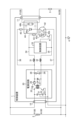
- FIG. 1 is a diagram showing a configuration example of a control device according to a first embodiment
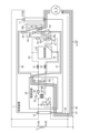
- FIG. 1 is a diagram showing an image of a parasitic capacitance present in a control device according to a first embodiment
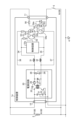
- FIG. 1 is a diagram showing an image of a circuit when a load connected to the control device according to the first embodiment becomes a noise source of common mode noise
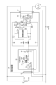
- FIG. 1 is a diagram showing an example of a path through which common mode noise flows in a control device according to a first embodiment
- FIG. 13 is a diagram showing a configuration example of a control device according to a second embodiment
- FIG. 13 is a diagram showing an image of a parasitic capacitance present in a control device according to a second embodiment
- FIG. 13 is a diagram showing an image of a circuit when a switch connected to a control device according to a second embodiment becomes a noise source of common mode noise.
- FIG. 13 is a diagram showing an example of a path through which common mode noise flows in a control device according to a second embodiment;
- FIG. 1 is a diagram showing a configuration example of a control device 1 according to a first embodiment.
- the control device 1 is a digital output (DO) circuit used in a train (not shown) or the like.
- the control device 1 is connected to a vehicle power source 2 and a load 3.
- the control device 1 controls the supply of power from the vehicle power source 2 to the load 3 under the control of a control circuit 33, and controls the operation of the load 3.
- the control device 1 includes connection units 10 and 11, a power supply circuit 20, a first power supply line 34 in which an inductor 31 is arranged, a first power supply line 35 in which an inductor 32 is arranged, a control circuit 33, second power supply lines 36 and 37, a transistor 41, a photocoupler 42, resistors 43 and 45, and a photo MOSFET (Metal-Oxide-Semiconductor Field-Effect Transistor) relay (hereinafter referred to as a photo MOS relay) 44.
- the power supply circuit 20 includes Y capacitors 21, 22, 28, and 29, a switching element 23, a transformer 24, capacitors 25 and 27, and a diode 26.
- the photocoupler 42 may be referred to as a first non-contact relay
- the photoMOS relay 44 may be referred to as a second non-contact relay.
- the control device 1 is connected to the positive pole P100 of the vehicle power supply 2 at one end of the connection part 10, and to the negative pole N100 of the vehicle power supply 2 at the other end of the connection part 10.
- the control device 1 is also connected to the positive pole P100 of the vehicle power supply 2 at one end of the connection part 11, and to the negative pole N100 of the vehicle power supply 2 at the other end of the connection part 11 via the load 3.
- the other end of the connection part 11 is an OUTPUT terminal.
- the load 3 is an external configuration having one end connected to the other end of the connection part 11 of the control device 1 and the other end connected to the negative pole N100 of the vehicle power supply 2.
- the load 3 is, for example, an on-board device mounted on a train (not shown).
- connection point of the Y capacitors 21 and 22, the connection point of the Y capacitors 28 and 29, the negative pole N100 of the vehicle power supply 2, the other end of the connection part 10 of the control device 1, and the other end of the load 3 are connected to the FG (Frame Ground) 4.
- FG4 is, for example, the body of a train (not shown).
- the power supply circuit 20 is a DC/DC converter that converts the voltage of the power supplied from the vehicle power supply 2 into a voltage that drives the control circuit 33, the photocoupler 42, and the photoMOS relay 44.
- the power supply circuit 20 includes a Y capacitor 21 between the positive side of the power supply input and FG4, a Y capacitor 22 between the negative side of the power supply input and FG4, a capacitor 25 between the primary and secondary sides of the transformer 24, a Y capacitor 28 between the positive side of the power supply output and FG4, and a Y capacitor 29 between the negative side of the power supply output and FG4, in order to counter switching noise caused by switching performed by the switching element 23.
- the configuration of the power supply circuit 20 is a general configuration, so a detailed description of the operation of the power supply circuit 20 will be omitted. Note that the configuration of the power supply circuit 20 is not limited to the example shown in FIG. 1.
- the power supply circuit 20 may have a configuration different from the configuration shown in FIG. 1 as long as it includes a Y capacitor.
- Inductors 31 and 32 are arranged on the first power supply lines 34 and 35. Specifically, as shown in FIG. 1, inductor 31 is arranged on the first power supply line 34, and inductor 32 is arranged on the first power supply line 35. That is, the control device 1 has two first power supply lines 34 and 35, each of which has an inductor arranged thereon.
- the first power supply lines 34 and 35, on which the inductors 31 and 32 are arranged, are power supply lines that supply the first power from the power supply circuit 20 to the control circuit 33 and the first input end to which the light-emitting diode 42a of the photocoupler 42 is connected.
- the control device 1 has two second power supply lines 36, 37 on which no inductor is disposed.
- the second power supply lines 36, 37 are power supply lines that supply the second power from the power supply circuit 20 to a first output terminal to which the light receiving element 42b of the photocoupler 42 is connected, and to a second input terminal to which the light emitting diode 44a of the photoMOS relay 44 is connected.
- the control circuit 33 receives a first power supply from the power supply circuit 20 via two first power supply lines 34, 35.
- the control circuit 33 controls the base current of the transistor 41 to control the on/off state of the transistor 41. By turning the transistor 41 on and off, the control circuit 33 can ultimately control the operation of the load 3.
- the transistor 41 is controlled to be turned on and off by the control circuit 33.
- the transistor 41 When the transistor 41 is turned on under the control of the control circuit 33, it conducts the first power to the light-emitting diode 42a at the first input end of the photocoupler 42, causing the light-emitting diode 42a to emit light.
- the resistor 43 is a resistor for adjusting the magnitude of the first power supplied from the power supply circuit 20.
- the resistor 45 is a resistor for adjusting the magnitude of the second power supplied from the power supply circuit 20.
- the photocoupler 42 includes a light-emitting diode 42a and a light-receiving element 42b.
- the photocoupler 42 also has a first input end and a first output end, with the light-emitting diode 42a connected to the first input end and the light-receiving element 42b connected to the first output end.
- the light-emitting diode 42a at the first input end is supplied with a first power from the power supply circuit 20 via two first power supply lines 34, 35
- the light-receiving element 42b at the first output end is supplied with a second power from the power supply circuit 20 via two second power supply lines 36, 37.
- the photoMOS relay 44 includes a light-emitting diode 44a and a light-receiving element 44b.
- the photoMOS relay 44 also has a second input end and a second output end, with the light-emitting diode 44a connected to the second input end and the light-receiving element 44b connected to the second output end.
- the light-emitting diode 44a at the second input end is supplied with the second power from the power supply circuit 20 via the two second power supply lines 36, 37
- the light-receiving element 44b at the second output end is supplied with the third power from the vehicle power supply 2 and is connected to the load 3, which is an external component.
- control circuit 33 can control the conduction of the first power to the light-emitting diode 42a at the first input end of the photocoupler 42 by controlling the on/off of the transistor 41 as described above.
- the control circuit 33 can conduct the first power to the light-emitting diode 42a at the first input end of the photocoupler 42, causing the light-emitting diode 42a at the first input end of the photocoupler 42 to emit light, thereby conducting the second power to the light-receiving element 42b at the first output end of the photocoupler 42.
- the control circuit 33 can conduct the second power to the light-receiving element 42b at the first output end of the photocoupler 42, thereby conducting the second power to the light-emitting diode 44a at the second input end of the photoMOS relay 44.
- the control circuit 33 conducts the second power to the light-emitting diode 44a at the second input end of the photoMOS relay 44, causing the light-emitting diode 44a at the second input end of the photoMOS relay 44 to emit light, and can conduct the third power from the vehicle power source 2 to the light-receiving element 44b at the second output end of the photoMOS relay 44.
- the control circuit 33 then conducts the third power from the vehicle power source 2 to the light-receiving element 44b at the second output end of the photoMOS relay 44, thereby supplying the third power from the vehicle power source 2 to the load 3 and controlling the operation of the load 3.
- FIG. 2 is a diagram showing an image of the parasitic capacitance present in the control device 1 according to the first embodiment.
- the control device 1 shown in FIG. 2 has additional parasitic capacitance inside the photocoupler 42 and photoMOS relay 44 compared to the control device 1 shown in FIG. 1, but in reality, parasitic capacitance also exists between the wires and between the wires and the housing.
- parasitic capacitance exists inside the control device 1 as shown in FIG.
- FIG. 3 is a diagram showing an image of a circuit when the load 3 connected to the control device 1 according to the first embodiment becomes a noise source of the common mode noise.
- the noise source can be considered to have a circuit configuration in which one end is connected to the other end of the connection part 11 of the control device 1 like the load 3, but the other end is connected to the FG 4. In such a case, if common mode noise flows into the control circuit 33, it is possible that the control circuit 33 may malfunction and affect the control of the load 3.
- inductors 31 and 32 are arranged on the first power supply lines 34 and 35 through which the first power is supplied from the power supply circuit 20 to the control circuit 33. Since the inductors 31 and 32 are arranged on the first power supply lines 34 and 35, the impedance of the first power supply lines 34 and 35 is larger than the impedance of the second power supply lines 36 and 37 on which no inductor is arranged. Therefore, even if common mode noise flows inside the control device 1, the common mode noise flows more in the second power supply lines 36 and 37, which have a smaller impedance, than in the first power supply lines 34 and 35 to which the control circuit 33 is connected. FIG.
- FIG. 4 is a diagram showing an example of paths 61 to 63 when common mode noise flows in the control device 1 according to the first embodiment.
- paths 61 to 63 when common mode noise flows in the control device 1 are added to FIG. 3. It is considered that the common mode noise flows mostly through the paths 61 and 62 and hardly flows through the path 63 due to the impedance relationship of each power supply line inside the control device 1 as described above.
- Path 61 is a path that returns from the noise source via connection 11, the parasitic capacitance of photoMOS relay 44, resistor 45, second power line 36, Y capacitor 28, the connection point of Y capacitors 28 and 29, and FG4.
- Path 62 is a path that returns from the noise source via connection 11, the parasitic capacitance of photoMOS relay 44, light receiving element 42b of photocoupler 42, second power line 37, Y capacitor 29, the connection point of Y capacitors 28 and 29, and FG4.
- Path 63 is a path that returns from the noise source via connection 11, the parasitic capacitance of photoMOS relay 44, the parasitic capacitance of photocoupler 42, transistor 41, control circuit 33, first power line 35, inductor 32, Y capacitor 29, the connection point of Y capacitors 28 and 29, and FG4.
- the path 63 may be a path that runs from the noise source through the connection 11, the parasitic capacitance of the photoMOS relay 44, the parasitic capacitance of the photocoupler 42, the transistor 41, the control circuit 33, the first power line 34, the inductor 31, the Y capacitor 28, the connection point of the Y capacitors 28 and 29, and the FG 4, and returns to the noise source.
- the paths 61 to 63 shown in FIG. 4 are examples, and parasitic capacitance may also exist between wires, between wires and the vehicle body, etc.
- the photocoupler 42 is used as the first non-contact relay
- the photoMOS relay 44 is used as the second non-contact relay
- the control device 1 may use a photoMOS relay as the first non-contact relay, and a photocoupler as the second non-contact relay.
- the control device 1 may also use photocouplers or photoMOS relays as both the first and second non-contact relays.
- the control device 1 may also use mechanical relays as the first and second non-contact relays. In this way, the control device 1 can use a photocoupler, a photoMOS relay, or a mechanical relay as the first and second non-contact relays.
- the control device 1 supplies the first power from the power supply circuit 20 to the control circuit 33 and the light emitting diode 42a at the first input end of the photocoupler 42, which is the first non-contact relay, via the first power supply line 34 on which the inductor 31 is arranged and the first power supply line 35 on which the inductor 32 is arranged.
- the control device 1 also supplies the second power from the power supply circuit 20 to the light receiving element 42b at the first output end of the photocoupler 42, which is the first non-contact relay, and the light emitting diode 44a at the second input end of the photoMOS relay 44, which is the second non-contact relay, via the second power supply lines 36 and 37.
- control device 1 can pass more common mode noise to the second power supply lines 36 and 37 than to the first power supply lines 34 and 35 to which the control circuit 33 is connected, thereby reducing malfunction of the control circuit 33 due to the common mode noise. That is, the control device 1 is equipped with a non-contact relay and can reduce the inflow of noise to a desired path via parasitic capacitance, specifically, to the first power supply lines 34 and 35 to which the control circuit 33 is connected.
- Embodiment 2 In the first embodiment, a DO circuit is specifically described as an example of the control device 1. In the second embodiment, a DI (Digital Input) circuit is specifically described as an example of the control device.
- DI Digital Input
- FIG. 5 is a diagram showing an example of the configuration of the control device 1a according to the second embodiment.
- the control device 1a is a DI circuit used in a train (not shown) or the like.
- the control device 1a is connected to a vehicle power source 2 and a switch 5.
- the control device 1a acquires operation information accepted by the switch 5 through a control circuit 33a.
- the control device 1a includes connection parts 10 and 11, a power supply circuit 20, a first power supply line 34 in which an inductor 31 is arranged, a first power supply line 35 in which an inductor 32 is arranged, a control circuit 33a, a second power supply line 36 and 37, resistors 51, 53, and 56, photocouplers 52 and 54, and a diode 55.
- the configuration of the power supply circuit 20 of the second embodiment shown in FIG. 5 is the same as the configuration of the power supply circuit 20 of the first embodiment shown in FIG. 1 and the like.
- the photocoupler 52 may be referred to as a first non-contact relay
- the photocoupler 54 may be referred to as a second non-contact relay.
- the control device 1a is connected to the positive pole P100 of the vehicle power supply 2 at one end of the connection part 10, and to the negative pole N100 of the vehicle power supply 2 at the other end of the connection part 10.
- the control device 1a is also connected to the positive pole P100 of the vehicle power supply 2 at one end of the connection part 11, and to the negative pole N100 of the vehicle power supply 2 at the other end of the connection part 11 via the switch 5.
- the other end of the connection part 11 is an INPUT terminal.
- the switch 5 is an external component having one end connected to the other end of the connection part 11 of the control device 1a and the other end connected to the negative pole N100 of the vehicle power supply 2.
- the switch 5 is, for example, an on-board device that accepts operations from a train crew member (not shown).
- the connection point of the Y capacitors 21 and 22, the connection point of the Y capacitors 28 and 29, the negative pole N100 of the vehicle power supply 2, the other end of the connection part 10 of the control device 1, and the other end of the switch 5
- Inductors 31 and 32 are arranged on the first power supply lines 34 and 35. Specifically, as shown in FIG. 5, inductor 31 is arranged on the first power supply line 34, and inductor 32 is arranged on the first power supply line 35. That is, the control device 1a has two first power supply lines 34 and 35, each of which has an inductor arranged thereon.
- the first power supply lines 34 and 35, on which the inductors 31 and 32 are arranged, are power supply lines that supply the first power from the power supply circuit 20 to the control circuit 33a and the first output end to which the light receiving element 52b of the photocoupler 52 is connected.
- the control device 1a has two second power supply lines 36, 37 on which no inductor is disposed.
- the second power supply lines 36, 37 are power supply lines that supply the second power from the power supply circuit 20 to a first input terminal to which the light-emitting diode 52a of the photocoupler 52 is connected, and to a second output terminal to which the light-receiving element 54b of the photocoupler 54 is connected.
- the control circuit 33a is supplied with the first power from the power supply circuit 20 via the two first power supply lines 34 and 35.
- the control circuit 33a acquires information on the operation accepted by the switch 5.
- Resistor 51 is a resistor for adjusting the magnitude of the first power supplied from power supply circuit 20.
- Resistor 53 is a resistor for adjusting the magnitude of the second power supplied from power supply circuit 20.
- Diode 55 is connected in parallel to photocoupler 54.
- Resistor 56 is a resistor for adjusting the magnitude of the third power supplied from vehicle power supply 2.
- the photocoupler 52 includes a light-emitting diode 52a and a light-receiving element 52b.
- the photocoupler 52 also has a first input end and a first output end, with the light-emitting diode 52a connected to the first input end and the light-receiving element 52b connected to the first output end.
- the light-receiving element 52b at the first output end is supplied with a first power from the power supply circuit 20 via two first power supply lines 34, 35
- the light-emitting diode 52a at the first input end is supplied with a second power from the power supply circuit 20 via two second power supply lines 36, 37.
- the photocoupler 54 includes a light-emitting diode 54a and a light-receiving element 54b.
- the photocoupler 54 also has a second input end and a second output end, with the light-emitting diode 54a connected to the second input end and the light-receiving element 54b connected to the second output end.
- the light-receiving element 54b at the second output end is supplied with the second power from the power supply circuit 20 via the two second power supply lines 36 and 37
- the light-emitting diode 54a at the second input end is supplied with the third power from the vehicle power supply 2 and is connected to the switch 5, which is an external component.
- a third power is conducted to the switch 5 and the light-emitting diode 54a at the second input end of the photocoupler 54 in response to the operation received by the switch 5, causing the light-emitting diode 54a at the second input end of the photocoupler 54 to emit light, and the second power is conducted to the light-receiving element 54b at the second output end of the photocoupler 54.
- the second power is conducted to the light-receiving element 54b at the second output end of the photocoupler 54, and therefore the second power is conducted to the light-emitting diode 52a at the first input end of the photocoupler 52.
- the control circuit 33a can obtain information on the operation accepted by the switch 5 based on the fluctuation of the first power conducted to the light-receiving element 52b at the first output end of the photocoupler 52.
- FIG. 6 is a diagram showing an image of the parasitic capacitances present in the control device 1a according to the second embodiment.
- the control device 1a shown in FIG. 6 has parasitic capacitances added inside the photocouplers 52 and 54 compared to the control device 1a shown in FIG. 5, but in reality, parasitic capacitances also exist between the wires and between the wires and the housing.
- parasitic capacitances exist inside the control device 1a as shown in FIG.
- FIG. 7 is a diagram showing an image of a circuit when the switch 5 connected to the control device 1a according to the second embodiment becomes a noise source of the common mode noise.
- the noise source can be considered to have a circuit configuration in which one end is connected to the other end of the connection part 11 of the control device 1a like the switch 5, but the other end is connected to the FG4. In such a case, if common mode noise flows into the control circuit 33a, it is possible that the control circuit 33a may malfunction, affecting the acquisition of information about the operation received by the switch 5.
- inductors 31 and 32 are arranged on the first power supply lines 34 and 35 through which the first power is supplied from the power supply circuit 20 to the control circuit 33a. Since the inductors 31 and 32 are arranged on the first power supply lines 34 and 35, the impedance of the first power supply lines 34 and 35 is larger than the impedance of the second power supply lines 36 and 37 on which no inductor is arranged. Therefore, even when common mode noise flows inside the control device 1a, the common mode noise flows more in the second power supply lines 36 and 37, which have a smaller impedance, than in the first power supply lines 34 and 35 to which the control circuit 33a is connected.
- Figure 8 is a diagram showing an example of paths 71 to 73 when common mode noise flows in the control device 1a according to the second embodiment.
- Figure 8 adds paths 71 to 73 when common mode noise flows in the control device 1a to FIG. 7. Due to the impedance relationships of the power supply lines inside the control device 1a described above, it is believed that most of the common mode noise flows through paths 71 and 72, and very little flows through path 73.
- Path 71 is a path that returns from the noise source via connection 11, the parasitic capacitance of photocoupler 54, light-emitting diode 52a of photocoupler 52, resistor 53, second power supply line 36, Y capacitor 28, the connection point of Y capacitors 28 and 29, and FG4.
- Path 72 is a path that returns from the noise source via connection 11, the parasitic capacitance of photocoupler 54, second power supply line 37, Y capacitor 29, the connection point of Y capacitors 28 and 29, and FG4.
- Path 73 is a path that returns from the noise source via connection 11, the parasitic capacitance of photocoupler 54, the parasitic capacitance of photocoupler 52, control circuit 33a, first power supply line 35, inductor 32, Y capacitor 29, the connection point of Y capacitors 28 and 29, and FG4.
- Path 73 may be a path that runs from the noise source through connection 11, the parasitic capacitance of photocoupler 54, the parasitic capacitance of photocoupler 52, control circuit 33a, first power line 34, inductor 31, Y capacitor 28, the connection point of Y capacitors 28 and 29, and FG4, and returns to the noise source.
- paths 71 to 73 shown in FIG. 8 are examples, and parasitic capacitance may also exist between wires, between wires and the vehicle body, etc.
- the photocoupler 52 is used as the first non-contact relay
- the photocoupler 54 is used as the second non-contact relay
- the control device 1a may use photoMOS relays as both the first non-contact relay and the second non-contact relay.
- the control device 1a may also use a photocoupler for one of the first non-contact relay and the second non-contact relay, and a photoMOS relay for the other.
- the control device 1a may also use mechanical relays as the first non-contact relay and the second non-contact relay. In this way, the control device 1a can use a photocoupler, a photoMOS relay, or a mechanical relay as the first non-contact relay and the second non-contact relay.
- the control device 1a supplies a first power from the power supply circuit 20 to the control circuit 33a and the light receiving element 52b at the first output end of the photocoupler 52, which is the first non-contact relay, via the first power supply line 34 on which the inductor 31 is arranged and the first power supply line 35 on which the inductor 32 is arranged.
- the control device 1a supplies a second power from the power supply circuit 20 to the light emitting diode 52a at the first input end of the photocoupler 52, which is the first non-contact relay, and the light receiving element 54b at the second output end of the photocoupler 54, which is the second non-contact relay, via the second power supply lines 36, 37.
- control device 1a can send more common mode noise to the second power lines 36 and 37 than to the first power lines 34 and 35 to which the control circuit 33a is connected, thereby reducing malfunction of the control circuit 33a due to common mode noise.
- the control device 1a is equipped with a non-contact relay and can reduce the inflow of noise to the desired path via parasitic capacitance, specifically the first power lines 34 and 35 to which the control circuit 33a is connected.
- the first power is supplied to the light-emitting diode 42a at the first input end, and the second power is supplied to the light-receiving element 42b at the first output end
- the photoMOS relay 44 which is the second non-contact relay, the second power is supplied to the light-emitting diode 44a at the second input end, and the third power is supplied to the light-receiving element 44b at the second output end.
- the control device 1a of the second embodiment in the photocoupler 52 which is the first non-contact relay, the first power is supplied to the light-receiving element 52b at the first output end, and the second power is supplied to the light-emitting diode 52a at the first input end, and in the photocoupler 54 which is the second non-contact relay, the second power is supplied to the light-receiving element 54b at the second output end, and the third power is supplied to the light-emitting diode 54a at the second input end.
- control device 1 of embodiment 1 and the control device 1a of embodiment 2 have different powers supplied to the input terminals and output terminals of each non-contact relay, but can achieve the same effect as described above. That is, the control devices 1 and 1a only need to include a first non-contact relay having a first input terminal and a first output terminal, one of which is supplied with a first power from the power supply circuit 20 via the two first power lines 34 and 35, and the other of which is supplied with a second power from the power supply circuit 20 via the two second power lines 36 and 37, and a second non-contact relay having a second input terminal and a second output terminal, one of which is supplied with a second power from the power supply circuit 20 via the two second power lines 36 and 37, and the other of which is supplied with a third power and is connected to an external configuration.
- 1, 1a control device 2 vehicle power supply, 3 load, 4 FG, 5 switch, 10, 11 connection, 20 power supply circuit, 21, 22, 28, 29 Y capacitor, 23 switching element, 24 transformer, 25, 27 capacitor, 26, 55 diode, 31, 32 inductor, 33, 33a control circuit, 34, 35 first power supply line, 36, 37 second power supply line, 41 transistor, 42, 52, 54 photocoupler, 42a, 44a, 52a, 54a light-emitting diode, 42b, 44b, 52b, 54b light-receiving element, 43, 45, 51, 53, 56 resistor, 44 photoMOS relay, 61-63, 71-73 path.
Landscapes
- Electronic Switches (AREA)
Abstract
制御装置(1)は、各々にインダクタ(31,32)が配置された2つの第1の電源ライン(34,35)と、2つの第2の電源ライン(36,37)と、電源回路(20)から2つの第1の電源ライン(34,35)を介して第1の電力が供給される制御回路(33)と、第1の入力端および第1の出力端を有し、一方に電源回路(20)から2つの第1の電源ライン(34,35)を介して第1の電力が供給され、他方に電源回路(20)から2つの第2の電源ライン(36,37)を介して第2の電力が供給される第1の非接触型リレーと、第2の入力端および第2の出力端を有し、一方に電源回路(20)から2つの第2の電源ライン(36,37)を介して第2の電力が供給され、他方に第3の電力が供給されるとともに外部構成が接続される第2の非接触型リレーと、を備える。
Description
本開示は、非接触型リレーを備える制御装置に関する。
従来、電車などで使用される制御装置は、一方の回路と他方の回路とを絶縁するため、フォトカプラなどの非接触型リレーを用いる。例えば、特許文献1には、電車で使用される外部条件入力回路において、半導体DC(Direct Current)/DCコンバータからの出力を、非接触型リレーであるフォトカプラを介して、動作信号情報デジタル信号として信号読み込み部に出力する技術が開示されている。
フォトカプラの内部に存在する寄生容量、配線経路に存在する寄生容量などによって、フォトカプラの1次側と2次側との間、すなわち発光ダイオード側と受光素子側との間は、結合されているとみなすことができる。このような回路を使用した場合、フォトカプラ付近に存在する寄生容量によって、フォトカプラの2次側に印加されたノイズはフォトカプラの1次側を流れてから車体に戻る、または、フォトカプラの1次側に印加されたノイズはフォトカプラの2次側を流れてから車体に戻る。そのため、制御回路がフォトカプラを介してノイズ源と接続されているような回路構成の場合、ノイズがフォトカプラを介して制御回路内を流れることによって制御回路が誤動作する可能性がある、という問題があった。
本開示は、上記に鑑みてなされたものであって、非接触型リレーを備えつつ、寄生容量を介した所望の経路へのノイズの流入を低減可能な制御装置を得ることを目的とする。
上述した課題を解決し、目的を達成するために、本開示の制御装置は、各々にインダクタが配置された2つの第1の電源ラインと、2つの第2の電源ラインと、電源回路から2つの第1の電源ラインを介して第1の電力が供給される制御回路と、第1の入力端および第1の出力端を有し、一方に電源回路から2つの第1の電源ラインを介して第1の電力が供給され、他方に電源回路から2つの第2の電源ラインを介して第2の電力が供給される第1の非接触型リレーと、第2の入力端および第2の出力端を有し、一方に電源回路から2つの第2の電源ラインを介して第2の電力が供給され、他方に第3の電力が供給されるとともに外部構成が接続される第2の非接触型リレーと、を備えることを特徴とする。
本開示の制御装置は、非接触型リレーを備えつつ、寄生容量を介した所望の経路へのノイズの流入を低減可能である、という効果を奏する。
以下に、本開示の実施の形態に係る制御装置を図面に基づいて詳細に説明する。
実施の形態1.
図1は、実施の形態1に係る制御装置1の構成例を示す図である。制御装置1は、図示しない電車などで使用されるDO(Degital Output)回路である。制御装置1は、車両電源2、および負荷3に接続される。制御装置1は、制御回路33の制御によって、車両電源2から負荷3への電力の供給を制御し、負荷3の動作を制御する。制御装置1は、接続部10,11と、電源回路20と、インダクタ31が配置された第1の電源ライン34と、インダクタ32が配置された第1の電源ライン35と、制御回路33と、第2の電源ライン36,37と、トランジスタ41と、フォトカプラ42と、抵抗43,45と、フォトMOSFET(Metal-Oxide-Semiconductor Field-Effect Transistor)リレー(以下、フォトMOSリレーと称する。)44と、を備える。電源回路20は、Yコンデンサ21,22,28,29と、スイッチング素子23と、トランス24と、コンデンサ25,27と、ダイオード26と、を備える。以降の説明において、フォトカプラ42を第1の非接触型リレーと称し、フォトMOSリレー44を第2の非接触型リレーと称することがある。
図1は、実施の形態1に係る制御装置1の構成例を示す図である。制御装置1は、図示しない電車などで使用されるDO(Degital Output)回路である。制御装置1は、車両電源2、および負荷3に接続される。制御装置1は、制御回路33の制御によって、車両電源2から負荷3への電力の供給を制御し、負荷3の動作を制御する。制御装置1は、接続部10,11と、電源回路20と、インダクタ31が配置された第1の電源ライン34と、インダクタ32が配置された第1の電源ライン35と、制御回路33と、第2の電源ライン36,37と、トランジスタ41と、フォトカプラ42と、抵抗43,45と、フォトMOSFET(Metal-Oxide-Semiconductor Field-Effect Transistor)リレー(以下、フォトMOSリレーと称する。)44と、を備える。電源回路20は、Yコンデンサ21,22,28,29と、スイッチング素子23と、トランス24と、コンデンサ25,27と、ダイオード26と、を備える。以降の説明において、フォトカプラ42を第1の非接触型リレーと称し、フォトMOSリレー44を第2の非接触型リレーと称することがある。
制御装置1は、車両電源2の正極P100と接続部10の一端で接続し、車両電源2の負極N100と接続部10の他端で接続する。また、制御装置1は、車両電源2の正極P100と接続部11の一端で接続し、車両電源2の負極N100と接続部11の他端で、負荷3を介して接続する。接続部11の他端は、OUTPUT端子である。負荷3は、一端が制御装置1の接続部11の他端に接続され、他端が車両電源2の負極N100に接続される外部構成である。負荷3は、例えば、図示しない電車などに搭載される車載機器である。なお、Yコンデンサ21,22の接続点、Yコンデンサ28,29の接続点、車両電源2の負極N100、制御装置1の接続部10の他端、および負荷3の他端は、FG(Frame Ground)4に接続されている。FG4は、例えば、図示しない電車の車体である。
制御装置1において、電源回路20は、車両電源2から供給された電力の電圧を制御回路33、フォトカプラ42、およびフォトMOSリレー44を駆動する電圧に変換するDC/DCコンバータである。電源回路20は、スイッチング素子23が行うスイッチングによるスイッチングノイズ対策などのため、電源入力の正側とFG4との間にYコンデンサ21を備え、電源入力の負側とFG4との間にYコンデンサ22を備え、トランス24の1次側と2次側との間にコンデンサ25を備え、電源出力の正側とFG4との間にYコンデンサ28を備え、電源出力の負側とFG4との間にYコンデンサ29を備えている。本実施の形態において、電源回路20の構成は一般的な構成であるので、電源回路20の詳細な動作の説明については省略する。なお、電源回路20の構成は、図1に示す例に限定されない。電源回路20は、Yコンデンサを備える構成であれば、図1に示す構成とは異なる構成であってもよい。
第1の電源ライン34,35には、インダクタ31,32が配置されている。具体的には、図1に示すように、第1の電源ライン34にはインダクタ31が配置され、第1の電源ライン35にはインダクタ32が配置されている。すなわち、制御装置1は、各々にインダクタが配置された2つの第1の電源ライン34,35を備えている。インダクタ31,32が配置されている第1の電源ライン34,35は、電源回路20からの第1の電力を、制御回路33、およびフォトカプラ42の発光ダイオード42aが接続される第1の入力端に供給する電源ラインである。
なお、第2の電源ライン36,37には、インダクタは配置されていない。すなわち、制御装置1は、インダクタが配置されていない2つの第2の電源ライン36,37を備えている。第2の電源ライン36,37は、電源回路20からの第2の電力を、フォトカプラ42の受光素子42bが接続される第1の出力端、およびフォトMOSリレー44の発光ダイオード44aが接続される第2の入力端に供給する電源ラインである。
制御回路33は、電源回路20から、2つの第1の電源ライン34,35を介して第1の電力が供給される。制御回路33は、トランジスタ41のベース電流を制御することでトランジスタ41のオンオフを制御する。制御回路33は、トランジスタ41をオンオフすることで、結果的に負荷3の動作を制御することができる。
トランジスタ41は、制御回路33によってオンオフが制御される。トランジスタ41は、制御回路33の制御によってオンすることで、第1の電力をフォトカプラ42の第1の入力端の発光ダイオード42aに導通させ、発光ダイオード42aを発光させることができる。抵抗43は、電源回路20から供給される第1の電力の大きさを調整するための抵抗である。抵抗45は、電源回路20から供給される第2の電力の大きさを調整するための抵抗である。
フォトカプラ42は、発光ダイオード42aと、受光素子42bと、を備える。また、フォトカプラ42は、第1の入力端および第1の出力端を有し、第1の入力端に発光ダイオード42aが接続され、第1の出力端に受光素子42bが接続される。図1に示すように、第1の入力端の発光ダイオード42aには、電源回路20から2つの第1の電源ライン34,35を介して第1の電力が供給され、第1の出力端の受光素子42bには、電源回路20から2つの第2の電源ライン36,37を介して第2の電力が供給される。
フォトMOSリレー44は、発光ダイオード44aと、受光素子44bと、を備える。また、フォトMOSリレー44は、第2の入力端および第2の出力端を有し、第2の入力端に発光ダイオード44aが接続され、第2の出力端に受光素子44bが接続される。図1に示すように、第2の入力端の発光ダイオード44aには、電源回路20から2つの第2の電源ライン36,37を介して第2の電力が供給され、第2の出力端の受光素子44bには、車両電源2から第3の電力が供給されるとともに外部構成である負荷3が接続される。
本実施の形態において、制御回路33は、前述のように、トランジスタ41のオンオフを制御することで、フォトカプラ42の第1の入力端の発光ダイオード42aにおける第1の電力の導通を制御可能である。制御回路33は、フォトカプラ42の第1の入力端の発光ダイオード42aに第1の電力を導通させることで、フォトカプラ42の第1の入力端の発光ダイオード42aが発光するので、フォトカプラ42の第1の出力端の受光素子42bに第2の電力を導通させることができる。フォトカプラ42の第1の出力端の受光素子42bとフォトMOSリレー44の第2の入力端の発光ダイオード44aとは直列接続されているので、制御回路33は、フォトカプラ42の第1の出力端の受光素子42bに第2の電力を導通させることで、フォトMOSリレー44の第2の入力端の発光ダイオード44aに第2の電力を導通させることができる。制御回路33は、フォトMOSリレー44の第2の入力端の発光ダイオード44aに第2の電力を導通させることで、フォトMOSリレー44の第2の入力端の発光ダイオード44aが発光するので、フォトMOSリレー44の第2の出力端の受光素子44bに車両電源2からの第3の電力を導通させることができる。そして、制御回路33は、フォトMOSリレー44の第2の出力端の受光素子44bに車両電源2からの第3の電力を導通させることで、負荷3に車両電源2からの第3の電力を供給させて負荷3の動作を制御することができる。
ここで、背景技術でも説明したように、フォトカプラ42、フォトMOSリレー44などでは、内部に寄生容量が存在することが想定される。図2は、実施の形態1に係る制御装置1に存在する寄生容量のイメージを示す図である。図2に示す制御装置1は、図1に示す制御装置1に対してフォトカプラ42およびフォトMOSリレー44の内部に寄生容量を追加しているが、実際には配線と配線との間、配線と筐体との間などにも寄生容量は存在する。図2に示すように制御装置1の内部に寄生容量が存在する場合、負荷3でコモンモードノイズが発生、すなわち負荷3がコモンモードノイズのノイズ源になると、コモンモードノイズが制御装置1の内部を流れてFG4からノイズ源に戻るループが発生する。図3は、実施の形態1に係る制御装置1に接続される負荷3がコモンモードノイズのノイズ源になった場合の回路のイメージを示す図である。図3に示すように、負荷3がコモンモードノイズのノイズ源になった場合、ノイズ源は、負荷3と同様に一端が制御装置1の接続部11の他端に接続されるが、他端がFG4に接続されるような回路構成とみなすことができる。このような場合、コモンモードノイズが制御回路33に流れると、制御回路33が誤動作し、負荷3の制御に影響を及ぼす可能性が考えられる。
しかしながら、本実施の形態では、電源回路20から制御回路33に第1の電力が供給される第1の電源ライン34,35には、インダクタ31,32が配置されている。第1の電源ライン34,35にインダクタ31,32が配置されていることから、第1の電源ライン34,35のインピーダンスは、インダクタが配置されていない第2の電源ライン36,37のインピーダンスよりも大きい。そのため、コモンモードノイズが制御装置1の内部を流れる場合でも、コモンモードノイズは、制御回路33が接続されている第1の電源ライン34,35よりも、インピーダンスの小さい第2の電源ライン36,37の方に多く流れることになる。図4は、実施の形態1に係る制御装置1にコモンモードノイズが流れる場合の経路61~63の例を示す図である。図4は、図3に対して、コモンモードノイズが制御装置1に流れるときの経路61~63を追加している。前述のような制御装置1の内部の各電源ラインのインピーダンスの関係から、コモンモードノイズは、大部分が経路61,62を流れ、経路63にはほとんど流れないと考えられる。
経路61は、ノイズ源から、接続部11、フォトMOSリレー44の寄生容量、抵抗45、第2の電源ライン36、Yコンデンサ28、Yコンデンサ28,29の接続点、およびFG4を経由してノイズ源に戻る経路である。経路62は、ノイズ源から、接続部11、フォトMOSリレー44の寄生容量、フォトカプラ42の受光素子42b、第2の電源ライン37、Yコンデンサ29、Yコンデンサ28,29の接続点、およびFG4を経由してノイズ源に戻る経路である。経路63は、ノイズ源から、接続部11、フォトMOSリレー44の寄生容量、フォトカプラ42の寄生容量、トランジスタ41、制御回路33、第1の電源ライン35、インダクタ32、Yコンデンサ29、Yコンデンサ28,29の接続点、およびFG4を経由してノイズ源に戻る経路である。なお、経路63は、ノイズ源から、接続部11、フォトMOSリレー44の寄生容量、フォトカプラ42の寄生容量、トランジスタ41、制御回路33、第1の電源ライン34、インダクタ31、Yコンデンサ28、Yコンデンサ28,29の接続点、およびFG4を経由してノイズ源に戻る経路としてもよい。なお、図4に示す経路61~63は例であって、配線と配線との間、配線と車体との間などにも寄生容量が存在することがある。
このように、負荷3がノイズ源となるコモンモードノイズが制御装置1に流れる場合、2つの第2の電源ライン36,37に流れるコモンモードノイズの合計量は、2つの第1の電源ライン34,35に流れるコモンモードノイズの合計量よりも大きくなる。
なお、本実施の形態では、第1の非接触型リレーとしてフォトカプラ42を用い、第2の非接触型リレーとしてフォトMOSリレー44を用いたが、これに限定されない。制御装置1は、第1の非接触型リレーとしてフォトMOSリレーを用い、第2の非接触型リレーとしてフォトカプラを用いてもよい。また、制御装置1は、第1の非接触型リレーおよび第2の非接触型リレーとして、ともにフォトカプラを用いてもよいし、ともにフォトMOSリレーを用いてもよい。また、制御装置1は、第1の非接触型リレーおよび第2の非接触型リレーとして、メカニカルリレーを用いることも可能である。このように、制御装置1は、第1の非接触型リレーおよび第2の非接触型リレーとして、フォトカプラ、またはフォトMOSリレー、またはメカニカルリレーを用いることができる。
以上説明したように、本実施の形態によれば、制御装置1は、電源回路20からインダクタ31が配置された第1の電源ライン34およびインダクタ32が配置された第1の電源ライン35を介して、制御回路33、および第1の非接触型リレーであるフォトカプラ42の第1の入力端の発光ダイオード42aに第1の電力を供給する。また、制御装置1は、電源回路20から第2の電源ライン36,37を介して、第1の非接触型リレーであるフォトカプラ42の第1の出力端の受光素子42b、および第2の非接触型リレーであるフォトMOSリレー44の第2の入力端の発光ダイオード44aに第2の電力を供給する。これにより、制御装置1は、負荷3をノイズ源とするコモンモードノイズが発生し、コモンモードノイズが制御装置1の内部を流れる場合でも、制御回路33が接続される第1の電源ライン34,35よりも第2の電源ライン36,37に多くのコモンモードノイズを流すことができるので、コモンモードノイズによる制御回路33の誤動作を低減することができる。すなわち、制御装置1は、非接触型リレーを備えつつ、寄生容量を介した所望の経路、具体的には制御回路33が接続される第1の電源ライン34,35へのノイズの流入を低減可能である。
実施の形態2.
実施の形態1では、制御装置1として、具体的に、DO回路を例にして説明した。実施の形態2では、制御装置として、具体的に、DI(Degital Input)回路を例にして説明する。
実施の形態1では、制御装置1として、具体的に、DO回路を例にして説明した。実施の形態2では、制御装置として、具体的に、DI(Degital Input)回路を例にして説明する。
図5は、実施の形態2に係る制御装置1aの構成例を示す図である。制御装置1aは、図示しない電車などで使用されるDI回路である。制御装置1aは、車両電源2、およびスイッチ5に接続される。制御装置1aは、スイッチ5で受け付けられた操作の情報を制御回路33aで取得する。制御装置1aは、接続部10,11と、電源回路20と、インダクタ31が配置された第1の電源ライン34と、インダクタ32が配置された第1の電源ライン35と、制御回路33aと、第2の電源ライン36,37と、抵抗51,53,56と、フォトカプラ52,54と、ダイオード55と、を備える。図5に示す実施の形態2の電源回路20の構成は、図1などに示す実施の形態1の電源回路20の構成と同様である。以降の説明において、フォトカプラ52を第1の非接触型リレーと称し、フォトカプラ54を第2の非接触型リレーと称することがある。
制御装置1aは、車両電源2の正極P100と接続部10の一端で接続し、車両電源2の負極N100と接続部10の他端で接続する。また、制御装置1aは、車両電源2の正極P100と接続部11の一端で接続し、車両電源2の負極N100と接続部11の他端で、スイッチ5を介して接続する。接続部11の他端は、INPUT端子である。スイッチ5は、一端が制御装置1aの接続部11の他端に接続され、他端が車両電源2の負極N100に接続される外部構成である。スイッチ5は、例えば、図示しない電車の乗務員からの操作を受け付ける車載機器である。なお、Yコンデンサ21,22の接続点、Yコンデンサ28,29の接続点、車両電源2の負極N100、制御装置1の接続部10の他端、およびスイッチ5の他端は、FG4に接続されている。
第1の電源ライン34,35には、インダクタ31,32が配置されている。具体的には、図5に示すように、第1の電源ライン34にはインダクタ31が配置され、第1の電源ライン35にはインダクタ32が配置されている。すなわち、制御装置1aは、各々にインダクタが配置された2つの第1の電源ライン34,35を備えている。インダクタ31,32が配置されている第1の電源ライン34,35は、電源回路20からの第1の電力を、制御回路33a、およびフォトカプラ52の受光素子52bが接続される第1の出力端に供給する電源ラインである。
なお、第2の電源ライン36,37には、インダクタは配置されていない。すなわち、制御装置1aは、インダクタが配置されていない2つの第2の電源ライン36,37を備えている。第2の電源ライン36,37は、電源回路20からの第2の電力を、フォトカプラ52の発光ダイオード52aが接続される第1の入力端、およびフォトカプラ54の受光素子54bが接続される第2の出力端に供給する電源ラインである。
制御回路33aは、電源回路20から、2つの第1の電源ライン34,35を介して第1の電力が供給される。制御回路33aは、スイッチ5で受け付けられた操作の情報を取得する。
抵抗51は、電源回路20から供給される第1の電力の大きさを調整するための抵抗である。抵抗53は、電源回路20から供給される第2の電力の大きさを調整するための抵抗である。ダイオード55は、フォトカプラ54に並列に接続される。抵抗56は、車両電源2から供給される第3の電力の大きさを調整するための抵抗である。
フォトカプラ52は、発光ダイオード52aと、受光素子52bと、を備える。また、フォトカプラ52は、第1の入力端および第1の出力端を有し、第1の入力端に発光ダイオード52aが接続され、第1の出力端に受光素子52bが接続される。図5に示すように、第1の出力端の受光素子52bには、電源回路20から2つの第1の電源ライン34,35を介して第1の電力が供給され、第1の入力端の発光ダイオード52aには、電源回路20から2つの第2の電源ライン36,37を介して第2の電力が供給される。
フォトカプラ54は、発光ダイオード54aと、受光素子54bと、を備える。また、フォトカプラ54は、第2の入力端および第2の出力端を有し、第2の入力端に発光ダイオード54aが接続され、第2の出力端に受光素子54bが接続される。図5に示すように、第2の出力端の受光素子54bには、電源回路20から2つの第2の電源ライン36,37を介して第2の電力が供給され、第2の入力端の発光ダイオード54aには、車両電源2から第3の電力が供給されるとともに外部構成であるスイッチ5が接続される。
本実施の形態において、制御装置1aでは、スイッチ5で受け付けられた操作に応じてスイッチ5およびフォトカプラ54の第2の入力端の発光ダイオード54aに第3の電力が導通することで、フォトカプラ54の第2の入力端の発光ダイオード54aが発光するので、フォトカプラ54の第2の出力端の受光素子54bに第2の電力が導通する。フォトカプラ54の第2の出力端の受光素子52bとフォトカプラ52の第1の入力端の発光ダイオード52aとは直列接続されているので、制御装置1aでは、フォトカプラ54の第2の出力端の受光素子54bに第2の電力が導通することで、フォトカプラ52の第1の入力端の発光ダイオード52aに第2の電力が導通する。フォトカプラ52の第1の入力端の発光ダイオード52aに第2の電力が導通することで、フォトカプラ52の第1の入力端の発光ダイオード52aが発光するので、フォトカプラ52の第1の出力端の受光素子52bに第1の電力が導通する。フォトカプラ52の第1の出力端の受光素子52bに第1の電力が導通することで、制御回路33aで検出可能な第1の電力が変動するが、第1の電力の変動は、スイッチ5で受け付けられた操作に応じた変動になる。そのため、制御回路33aは、フォトカプラ52の第1の出力端の受光素子52bに導通する第1の電力の変動に基づいて、スイッチ5で受け付けられた操作の情報を取得することができる。
ここで、背景技術でも説明したように、フォトカプラ52,54などでは、内部に寄生容量が存在することが想定される。図6は、実施の形態2に係る制御装置1aに存在する寄生容量のイメージを示す図である。図6に示す制御装置1aは、図5に示す制御装置1aに対してフォトカプラ52,54の内部に寄生容量を追加しているが、実際には配線と配線との間、配線と筐体との間などにも寄生容量は存在する。図6に示すように制御装置1aの内部に寄生容量が存在する場合、スイッチ5でコモンモードノイズが発生、すなわちスイッチ5がコモンモードノイズのノイズ源になると、コモンモードノイズが制御装置1aの内部を流れてFG4からノイズ源に戻るループが発生する。図7は、実施の形態2に係る制御装置1aに接続されるスイッチ5がコモンモードノイズのノイズ源になった場合の回路のイメージを示す図である。図7に示すように、スイッチ5がコモンモードノイズのノイズ源になった場合、ノイズ源は、スイッチ5と同様に一端が制御装置1aの接続部11の他端に接続されるが、他端がFG4に接続されるような回路構成とみなすことができる。このような場合、コモンモードノイズが制御回路33aに流れると、制御回路33aが誤動作し、スイッチ5で受け付けられた操作の情報の取得に影響を及ぼす可能性が考えられる。
しかしながら、本実施の形態では、電源回路20から制御回路33aに第1の電力が供給される第1の電源ライン34,35には、インダクタ31,32が配置されている。第1の電源ライン34,35にインダクタ31,32が配置されていることから、第1の電源ライン34,35のインピーダンスは、インダクタが配置されていない第2の電源ライン36,37のインピーダンスよりも大きい。そのため、コモンモードノイズが制御装置1aの内部を流れる場合でも、コモンモードノイズは、制御回路33aが接続されている第1の電源ライン34,35よりも、インピーダンスの小さい第2の電源ライン36,37の方に多く流れることになる。図8は、実施の形態2に係る制御装置1aにコモンモードノイズが流れる場合の経路71~73の例を示す図である。図8は、図7に対して、コモンモードノイズが制御装置1aに流れるときの経路71~73を追加している。前述のような制御装置1aの内部の各電源ラインのインピーダンスの関係から、コモンモードノイズは、大部分が経路71,72を流れ、経路73にはほとんど流れないと考えられる。
経路71は、ノイズ源から、接続部11、フォトカプラ54の寄生容量、フォトカプラ52の発光ダイオード52a、抵抗53、第2の電源ライン36、Yコンデンサ28、Yコンデンサ28,29の接続点、およびFG4を経由してノイズ源に戻る経路である。経路72は、ノイズ源から、接続部11、フォトカプラ54の寄生容量、第2の電源ライン37、Yコンデンサ29、Yコンデンサ28,29の接続点、およびFG4を経由してノイズ源に戻る経路である。経路73は、ノイズ源から、接続部11、フォトカプラ54の寄生容量、フォトカプラ52の寄生容量、制御回路33a、第1の電源ライン35、インダクタ32、Yコンデンサ29、Yコンデンサ28,29の接続点、およびFG4を経由してノイズ源に戻る経路である。なお、経路73は、ノイズ源から、接続部11、フォトカプラ54の寄生容量、フォトカプラ52の寄生容量、制御回路33a、第1の電源ライン34、インダクタ31、Yコンデンサ28、Yコンデンサ28,29の接続点、およびFG4を経由してノイズ源に戻る経路としてもよい。なお、図8に示す経路71~73は例であって、配線と配線との間、配線と車体との間などにも寄生容量が存在することがある。
このように、スイッチ5がノイズ源となるコモンモードノイズが制御装置1aに流れる場合、2つの第2の電源ライン36,37に流れるコモンモードノイズの合計量は、2つの第1の電源ライン34,35に流れるコモンモードノイズの合計量よりも大きくなる。
なお、本実施の形態では、第1の非接触型リレーとしてフォトカプラ52を用い、第2の非接触型リレーとしてフォトカプラ54を用いたが、これに限定されない。制御装置1aは、第1の非接触型リレーおよび第2の非接触型リレーとして、ともにフォトMOSリレーを用いてもよい。また、制御装置1aは、第1の非接触型リレーおよび第2の非接触型リレーのうち、一方をフォトカプラ、他方をフォトMOSリレーとして用いてもよい。また、制御装置1aは、第1の非接触型リレーおよび第2の非接触型リレーとして、メカニカルリレーを用いることも可能である。このように、制御装置1aは、第1の非接触型リレーおよび第2の非接触型リレーとして、フォトカプラ、またはフォトMOSリレー、またはメカニカルリレーを用いることができる。
以上説明したように、本実施の形態によれば、制御装置1aは、電源回路20からインダクタ31が配置された第1の電源ライン34およびインダクタ32が配置された第1の電源ライン35を介して、制御回路33a、および第1の非接触型リレーであるフォトカプラ52の第1の出力端の受光素子52bに第1の電力を供給する。また、制御装置1aは、電源回路20から第2の電源ライン36,37を介して、第1の非接触型リレーであるフォトカプラ52の第1の入力端の発光ダイオード52a、および第2の非接触型リレーであるフォトカプラ54の第2の出力端の受光素子54bに第2の電力を供給する。これにより、制御装置1aは、スイッチ5をノイズ源とするコモンモードノイズが発生し、コモンモードノイズが制御装置1aの内部を流れる場合でも、制御回路33aが接続される第1の電源ライン34,35よりも第2の電源ライン36,37に多くのコモンモードノイズを流すことができるので、コモンモードノイズによる制御回路33aの誤動作を低減することができる。すなわち、制御装置1aは、非接触型リレーを備えつつ、寄生容量を介した所望の経路、具体的には制御回路33aが接続される第1の電源ライン34,35へのノイズの流入を低減可能である。
ここで、実施の形態1の制御装置1において、第1の非接触型リレーであるフォトカプラ42では、第1の入力端の発光ダイオード42aに第1の電力が供給され、第1の出力端の受光素子42bに第2の電力が供給され、第2の非接触型リレーであるフォトMOSリレー44では、第2の入力端の発光ダイオード44aに第2の電力が供給され、第2の出力端の受光素子44bに第3の電力が供給される。これに対して、実施の形態2の制御装置1aにおいて、第1の非接触型リレーであるフォトカプラ52では、第1の出力端の受光素子52bに第1の電力が供給され、第1の入力端の発光ダイオード52aに第2の電力が供給され、第2の非接触型リレーであるフォトカプラ54では、第2の出力端の受光素子54bに第2の電力が供給され、第2の入力端の発光ダイオード54aに第3の電力が供給される。
このように、実施の形態1の制御装置1および実施の形態2の制御装置1aは、各非接触型リレーの入力端および出力端に供給される電力が異なっているが、前述のように同様の効果を得ることができる。すなわち、制御装置1,1aは、第1の入力端および第1の出力端を有し、一方に電源回路20から2つの第1の電源ライン34,35を介して第1の電力が供給され、他方に電源回路20から2つの第2の電源ライン36,37を介して第2の電力が供給される第1の非接触型リレーと、第2の入力端および第2の出力端を有し、一方に電源回路20から2つの第2の電源ライン36,37を介して第2の電力が供給され、他方に第3の電力が供給されるとともに外部構成が接続される第2の非接触型リレーと、を備えていればよい。
以上の実施の形態に示した構成は、一例を示すものであり、別の公知の技術と組み合わせることも可能であるし、実施の形態同士を組み合わせることも可能であるし、要旨を逸脱しない範囲で、構成の一部を省略、変更することも可能である。
1,1a 制御装置、2 車両電源、3 負荷、4 FG、5 スイッチ、10,11 接続部、20 電源回路、21,22,28,29 Yコンデンサ、23 スイッチング素子、24 トランス、25,27 コンデンサ、26,55 ダイオード、31,32 インダクタ、33,33a 制御回路、34,35 第1の電源ライン、36,37 第2の電源ライン、41 トランジスタ、42,52,54 フォトカプラ、42a,44a,52a,54a 発光ダイオード、42b,44b,52b,54b 受光素子、43,45,51,53,56 抵抗、44 フォトMOSリレー、61~63,71~73 経路。
Claims (6)
- 各々にインダクタが配置された2つの第1の電源ラインと、
2つの第2の電源ラインと、
電源回路から前記2つの第1の電源ラインを介して第1の電力が供給される制御回路と、
第1の入力端および第1の出力端を有し、一方に前記電源回路から前記2つの第1の電源ラインを介して前記第1の電力が供給され、他方に前記電源回路から前記2つの第2の電源ラインを介して第2の電力が供給される第1の非接触型リレーと、
第2の入力端および第2の出力端を有し、一方に前記電源回路から前記2つの第2の電源ラインを介して前記第2の電力が供給され、他方に第3の電力が供給されるとともに外部構成が接続される第2の非接触型リレーと、
を備えることを特徴とする制御装置。 - 前記外部構成は負荷であり、
前記制御回路は、
前記第1の非接触型リレーの前記第1の入力端における前記第1の電力の導通を制御可能であり、
前記第1の非接触型リレーの前記第1の入力端に前記第1の電力を導通させることで前記第1の非接触型リレーの前記第1の出力端に前記第2の電力を導通させ、
前記第1の非接触型リレーの前記第1の出力端に前記第2の電力を導通させることで前記第2の非接触型リレーの前記第2の入力端に前記第2の電力を導通させ、
前記第2の非接触型リレーの前記第2の入力端に前記第2の電力を導通させることで前記第2の非接触型リレーの前記第2の出力端に前記第3の電力を導通させ、
前記第2の非接触型リレーの前記第2の出力端に前記第3の電力を導通させることで前記負荷に前記第3の電力を供給させて前記負荷の動作を制御する、
ことを特徴とする請求項1に記載の制御装置。 - 前記負荷がノイズ源となるコモンモードノイズが前記制御装置に流れる場合、前記2つの第2の電源ラインに流れる前記コモンモードノイズの合計量は、前記2つの第1の電源ラインに流れる前記コモンモードノイズの合計量よりも大きい、
ことを特徴とする請求項2に記載の制御装置。 - 前記外部構成はスイッチであり、
前記スイッチで受け付けられた操作に応じて前記スイッチおよび前記第2の非接触型リレーの前記第2の入力端に前記第3の電力が導通することで前記第2の非接触型リレーの前記第2の出力端に前記第2の電力が導通し、
前記第2の非接触型リレーの前記第2の出力端に前記第2の電力が導通することで前記第1の非接触型リレーの前記第1の入力端に前記第2の電力が導通し、
前記第1の非接触型リレーの前記第1の入力端に前記第2の電力が導通することで前記第1の非接触型リレーの前記第1の出力端に前記第1の電力が導通し、
前記第1の非接触型リレーの前記第1の出力端に前記第1の電力が導通することで、
前記制御回路は、前記第1の非接触型リレーの前記第1の出力端に導通する前記第1の電力の変動に基づいて、前記スイッチで受け付けられた操作の情報を取得する、
ことを特徴とする請求項1に記載の制御装置。 - 前記スイッチがノイズ源となるコモンモードノイズが前記制御装置に流れる場合、前記2つの第2の電源ラインに流れる前記コモンモードノイズの合計量は、前記2つの第1の電源ラインに流れる前記コモンモードノイズの合計量よりも大きい、
ことを特徴とする請求項4に記載の制御装置。 - 前記第1の非接触型リレーおよび前記第2の非接触型リレーは、フォトカプラ、またはフォトMetal-Oxide-Semiconductor Field-Effect Transistorリレー、またはメカニカルリレーである、
ことを特徴とする請求項1から5のいずれか1つに記載の制御装置。
Priority Applications (2)
| Application Number | Priority Date | Filing Date | Title |
|---|---|---|---|
| PCT/JP2023/021482 WO2024252657A1 (ja) | 2023-06-09 | 2023-06-09 | 制御装置 |
| JP2025523961A JP7728490B2 (ja) | 2023-06-09 | 2023-06-09 | 制御装置 |
Applications Claiming Priority (1)
| Application Number | Priority Date | Filing Date | Title |
|---|---|---|---|
| PCT/JP2023/021482 WO2024252657A1 (ja) | 2023-06-09 | 2023-06-09 | 制御装置 |
Publications (1)
| Publication Number | Publication Date |
|---|---|
| WO2024252657A1 true WO2024252657A1 (ja) | 2024-12-12 |
Family
ID=93795575
Family Applications (1)
| Application Number | Title | Priority Date | Filing Date |
|---|---|---|---|
| PCT/JP2023/021482 Ceased WO2024252657A1 (ja) | 2023-06-09 | 2023-06-09 | 制御装置 |
Country Status (2)
| Country | Link |
|---|---|
| JP (1) | JP7728490B2 (ja) |
| WO (1) | WO2024252657A1 (ja) |
Citations (3)
| Publication number | Priority date | Publication date | Assignee | Title |
|---|---|---|---|---|
| JPS57200952U (ja) * | 1981-06-15 | 1982-12-21 | ||
| JPS5928724A (ja) * | 1982-08-10 | 1984-02-15 | Olympus Optical Co Ltd | フオト・カプラ信号処理回路 |
| JP2013106310A (ja) * | 2011-11-16 | 2013-05-30 | Panasonic Corp | 半導体スイッチ |
-
2023
- 2023-06-09 WO PCT/JP2023/021482 patent/WO2024252657A1/ja not_active Ceased
- 2023-06-09 JP JP2025523961A patent/JP7728490B2/ja active Active
Patent Citations (3)
| Publication number | Priority date | Publication date | Assignee | Title |
|---|---|---|---|---|
| JPS57200952U (ja) * | 1981-06-15 | 1982-12-21 | ||
| JPS5928724A (ja) * | 1982-08-10 | 1984-02-15 | Olympus Optical Co Ltd | フオト・カプラ信号処理回路 |
| JP2013106310A (ja) * | 2011-11-16 | 2013-05-30 | Panasonic Corp | 半導体スイッチ |
Also Published As
| Publication number | Publication date |
|---|---|
| JP7728490B2 (ja) | 2025-08-22 |
| JPWO2024252657A1 (ja) | 2024-12-12 |
Similar Documents
| Publication | Publication Date | Title |
|---|---|---|
| US8054106B2 (en) | Load driving device | |
| JP4034733B2 (ja) | フィードフォワード取り消しを備えた能動的emiフィルタ | |
| US9444445B2 (en) | Power switch driving circuits and power converters thereof | |
| US11209464B2 (en) | Current detection circuit and power converter | |
| JP2009075957A (ja) | 電源回路および半導体装置 | |
| EP0750803A1 (en) | Current protection method and apparatus and current protected low dropout voltage circuits | |
| CA2986883A1 (en) | Power conversion device | |
| WO2024252657A1 (ja) | 制御装置 | |
| WO2014192246A1 (ja) | 負荷制御装置 | |
| CN100448162C (zh) | 具有前馈补偿的有源电磁干扰滤波器 | |
| US11829179B2 (en) | Integrated circuit and method for limiting a switchable load current | |
| JP2023158375A (ja) | 電源回路 | |
| TW202236801A (zh) | 切換模組 | |
| US9099923B1 (en) | Hybrid power supply architecture | |
| JP6952493B2 (ja) | 通信システムおよび中継装置 | |
| US20250038712A1 (en) | Load drive circuit capable of stopping operating upon occurrence of abnormality, and method of controlling load drive circuit | |
| JP3739884B2 (ja) | 電源装置 | |
| US9941803B1 (en) | Controller IC device for a switched mode power converter and method for operating a controller IC device of a switched mode power converter | |
| JP2024063307A (ja) | 発光素子駆動装置 | |
| JPWO2018012168A1 (ja) | 電子制御装置 | |
| US20220311437A1 (en) | Electronic circuit | |
| JP3769527B2 (ja) | 電源回路および電子回路 | |
| JP2001061273A (ja) | ドライバ回路 | |
| KR200406392Y1 (ko) | 유도등 점등회로의 전압 스위칭회로 | |
| JPWO2024202425A5 (ja) |
Legal Events
| Date | Code | Title | Description |
|---|---|---|---|
| 121 | Ep: the epo has been informed by wipo that ep was designated in this application |
Ref document number: 23940755 Country of ref document: EP Kind code of ref document: A1 |
|
| WWE | Wipo information: entry into national phase |
Ref document number: 2025523961 Country of ref document: JP |
|
| NENP | Non-entry into the national phase |
Ref country code: DE |