WO2024252631A1 - 光送信器及び光送信器の制御方法 - Google Patents
光送信器及び光送信器の制御方法 Download PDFInfo
- Publication number
- WO2024252631A1 WO2024252631A1 PCT/JP2023/021408 JP2023021408W WO2024252631A1 WO 2024252631 A1 WO2024252631 A1 WO 2024252631A1 JP 2023021408 W JP2023021408 W JP 2023021408W WO 2024252631 A1 WO2024252631 A1 WO 2024252631A1
- Authority
- WO
- WIPO (PCT)
- Prior art keywords
- light
- wavelength
- light source
- optical
- optical transmitter
- Prior art date
- Legal status (The legal status is an assumption and is not a legal conclusion. Google has not performed a legal analysis and makes no representation as to the accuracy of the status listed.)
- Ceased
Links
Images









Classifications
-
- G—PHYSICS
- G02—OPTICS
- G02F—OPTICAL DEVICES OR ARRANGEMENTS FOR THE CONTROL OF LIGHT BY MODIFICATION OF THE OPTICAL PROPERTIES OF THE MEDIA OF THE ELEMENTS INVOLVED THEREIN; NON-LINEAR OPTICS; FREQUENCY-CHANGING OF LIGHT; OPTICAL LOGIC ELEMENTS; OPTICAL ANALOGUE/DIGITAL CONVERTERS
- G02F1/00—Devices or arrangements for the control of the intensity, colour, phase, polarisation or direction of light arriving from an independent light source, e.g. switching, gating or modulating; Non-linear optics
- G02F1/01—Devices or arrangements for the control of the intensity, colour, phase, polarisation or direction of light arriving from an independent light source, e.g. switching, gating or modulating; Non-linear optics for the control of the intensity, phase, polarisation or colour
- G02F1/015—Devices or arrangements for the control of the intensity, colour, phase, polarisation or direction of light arriving from an independent light source, e.g. switching, gating or modulating; Non-linear optics for the control of the intensity, phase, polarisation or colour based on semiconductor elements having potential barriers, e.g. having a PN or PIN junction
Definitions
- This disclosure relates to an optical transmitter and a method for controlling an optical transmitter.
- Patent Document 1 describes an LN (LiNbO 3 : lithium niobate) modulator constituting an MZ modulator and a control unit that controls the bias voltage of the LN modulator. Furthermore, Patent Documents 2 and 3 also describe a control unit that controls the wavelength of a light source input to the modulator.
- LN LiNbO 3 : lithium niobate
- Patent No. 5924349 JP 2008-228206 A Japanese Patent Application Publication No. 08-237203
- the present disclosure aims to provide an optical transmitter and a method for controlling an optical transmitter that can optimally control the bias of a modulator and the wavelength of a light source.
- the optical transmitter includes a light source that generates a light source light, a semiconductor modulator that modulates the generated light source light into modulated light, a splitter that branches the modulated light into output light and monitor light, an optical filter that transmits light in a transmission band from the branched monitor light, an optical monitor that monitors the transmitted light, a bias control means that controls the bias voltage of the semiconductor modulator based on the monitoring result, and a wavelength control means that controls the wavelength of the light source light based on the monitoring result.
- the method of controlling an optical transmitter generates source light using a light source, modulates the generated source light into modulated light using a semiconductor modulator, branches the modulated light into output light and monitor light, transmits light in a transmission band from the branched monitor light, monitors the transmitted light, controls the wavelength of the source light based on the monitoring result, and controls the bias voltage of the semiconductor modulator based on the monitoring result.
- the present disclosure provides an optical transmitter and a method for controlling an optical transmitter that can optimally control the bias of a modulator and the wavelength of a light source.
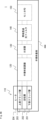
- FIG. 1 is a diagram showing a configuration of an optical transmitter according to a related technique.
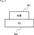
- 1 is a schematic side view showing an example of the arrangement of a temperature adjustment function of a light source in a related art.
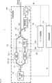
- 1 is a configuration diagram showing a configuration example of an optical transmitter according to a first embodiment;
- 2 is a schematic side view showing an example of an arrangement of each part in the semiconductor substrate according to the first embodiment;
- 10 is a schematic side view showing another example of the arrangement of each part in the semiconductor substrate according to the first embodiment.
- FIG. 2 is a configuration diagram showing a specific configuration example of the semiconductor modulator according to the first embodiment;
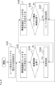
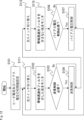
- 5 is a flowchart showing an example of the operation of the optical transmitter according to the first embodiment
- 5A to 5C are diagrams showing example spectra for explaining specific examples of wavelength control of the light source according to the first embodiment
- 5A to 5C are diagrams illustrating examples of monitor power for explaining specific examples of wavelength control of a light source according to the first embodiment
- 5A to 5C are diagrams showing example spectra for explaining specific examples of wavelength control of the light source according to the first embodiment
- 5A to 5C are diagrams illustrating examples of monitor power for explaining specific examples of wavelength control of a light source according to the first embodiment.
- FIG. 11 is a configuration diagram showing a configuration example of an optical transmitter according to a second embodiment.
- 11A and 11B are diagrams illustrating an example of a transmission band of a band-pass optical filter according to a second embodiment.
- 11 is a flowchart showing an example of the operation of the optical transmitter according to the second embodiment;
- FIG. 11 is a configuration diagram showing a configuration example of an optical transmitter according to a third embodiment.
- FIG. 11 is a configuration diagram showing a specific configuration example of a DP-IQ modulator according to a third embodiment.
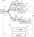
- FIG. 13 is a configuration diagram showing a configuration example of an optical transmitter according to a fourth embodiment.
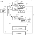
- FIG. 13 is a configuration diagram showing a configuration example of an optical transmitter according to a fifth embodiment.
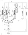
- FIG. 13 is a configuration diagram showing another configuration example of the optical transmitter according to the fifth embodiment.
- Fig. 1 shows the configuration of an optical transmitter 9 in the related technology based on the description of Patent Document 1, for example.
- Fig. 1 shows an example of the configuration of an optical transmitter using an LN modulator.
- the related optical transmitter 9 includes a light source 901, an LN modulator 902, a monitor PD 903, and a bias control unit 904.
- the light source 901 is an external light source provided outside the LN modulator 902, and is connected to the LN modulator 902 via an optical fiber or the like.
- the light source 901 is, for example, a DFB (Distributed Feedback) laser.
- the LN modulator 902 modulates the light output from the light source 901.
- the monitor PD 903 is a light receiving unit provided outside the LN modulator 902.
- the monitor PD 903 receives and monitors the light modulated by the LN modulator 902.
- the bias control unit 904 feedback controls the bias voltage of the LN modulator 902 according to the monitoring result of the monitor PD 903 so that the output deviation due to the bias point (operating point) vibration of the LN modulator 902 is reduced.
- a related technology is a wavelength control method that utilizes a temperature adjustment function.
- Figure 2 is a schematic side view showing an example of the arrangement of a temperature adjustment function of a light source in the related technology.
- a TEC Thermoelectric Cooler
- the wavelength of the light source 901 is controlled by adjusting the temperature of the entire surface below the light source 901 with the TEC 905.
- the light source is external to the LN modulator, and the temperature adjustment function of the light source is large, which is an obstacle to miniaturization.
- the LN modulator as a semiconductor modulator and the semiconductor modulator with the light source, it is difficult to locally control the wavelength of the light source with a large temperature adjustment function such as a TEC. Therefore, in the embodiment, it is possible to perform wavelength control of the light source and bias control of the semiconductor modulator in close proximity to each other in a small area.
- the light from the light source is split into two, and the split lights are input to an optical phase modulation section and an optical frequency shifter, respectively, and the output lights from the optical phase modulation section and the optical frequency shifter are combined.
- the distortion component control section controls the bias voltage applied to the optical phase modulation section based on the combined optical signal
- the light source control section controls the wavelength of the light source based on the optical signal from the optical frequency shifter.
- the optical signal output from the LN modulator is input to a bandpass filter, the optical signal that passes through the bandpass filter is branched by an optical coupler, and the bias voltage of the LN modulator and the wavelength of the light source are controlled based on the branched light. Since Patent Document 3 is based on the use of an LN modulator, the modulator and light source cannot be integrated. In addition, since the optical signal that passes through the bandpass filter is output to the optical transmission path, a large fluctuation in the wavelength of the light source may result in a disconnection of the signal, and depending on the amount of fluctuation, this may lead to a decrease in the power of the output light.
- Fig. 3 shows a configuration example of an optical transmitter 1 according to this embodiment.
- Fig. 4A and Fig. 4B are schematic side views showing an example of the arrangement of each part of the semiconductor substrate 200 in Fig. 3.
- Fig. 5 shows a specific configuration example of the semiconductor modulator 120 in Fig. 3.
- the optical transmitter 1 is, for example, an optical transmitter for digital coherent communication. As shown in FIG. 3, the optical transmitter 1 includes a single-wavelength light source 110, a semiconductor modulator 120, a splitter 130, a bandpass optical filter 140, a monitor PD 150, a bias control unit 160, and a wavelength control unit 170.
- the single-wavelength light source 110, the semiconductor modulator 120, the splitter 130, the bandpass optical filter 140, and the monitor PD 150 are formed on one semiconductor substrate 200. At least the single-wavelength light source 110 and the semiconductor modulator 120 may be formed on the semiconductor substrate 200.
- the semiconductor substrate 200 is, for example, a semiconductor substrate such as indium phosphide (InP), gallium arsenide (GaAs), or silicon (Si), but may also be another semiconductor substrate such as germanium (Ge).
- the bias control unit 160 and the wavelength control unit 170 are formed as a semiconductor chip separate from the semiconductor substrate 200.
- the bias control unit 160 and the wavelength control unit 170 may be configured as separate semiconductor chips or may be configured as a single semiconductor chip.
- the bias control unit 160 and the wavelength control unit 170 may be configured as hardware or software, or both.
- the functions of the bias control unit 160 and the wavelength control unit 170 may be implemented by executing a program stored in a memory in a processor such as a CPU (Central Processing Unit).
- a semiconductor chip including the bias control unit 160 and the wavelength control unit 170 may be mounted on the semiconductor substrate 200 by flip chip or the like.
- a semiconductor device including all the configurations in FIG. 3 may be formed as a single semiconductor package.
- the single-wavelength light source 110 generates source light SO1, which is light of a preset single wavelength (set wavelength).
- the single-wavelength light source 110 is a semiconductor laser formed on a semiconductor substrate 200 such as indium phosphide or silicon.
- the single-wavelength light source 110 may be, for example, a DFB laser or a DBR (Distributed Bragg Reflector) laser, or an external cavity laser (ECL).
- the single-wavelength light source 110 is a fixed-wavelength light source in which the set wavelength of the source light SO1 is fixed, but may also be a variable-wavelength light source in which the set wavelength of the source light SO1 is variable.
- the single-wavelength light source 110 is configured by, for example, stacking a lower clad layer 201, an active layer 202, and an upper clad layer 203 on a semiconductor substrate 200.
- a heater 204 is formed on the top of the single-wavelength light source 110 (semiconductor substrate 200), that is, on the upper clad layer 203.
- the heater 204 is a heating element capable of heating the single-wavelength light source 110.
- the heater 204 is formed of a temperature-controllable resistor such as a TiN heater.
- the heater 204 is formed in correspondence with the formation region of the single-wavelength light source 110 on the semiconductor substrate 200.
- the heater 204 may be formed within the range of the formation region of the single-wavelength light source 110.
- the heater 204 may have the same shape and size as the formation area (active layer 202) of the single-wavelength light source 110 in a plan view, or may have a shape and size smaller than the formation area of the single-wavelength light source 110.
- the heater 204 may be larger than the formation area of the single-wavelength light source 110, but it is preferable that the heater 204 does not overlap with the formation area of other optical devices such as the semiconductor modulator 120.
- the heater 204 generates heat according to the heater current HT supplied from the wavelength control unit 170, and the refractive index of the active layer 202 changes due to the heat of the heater 204, thereby controlling the wavelength of the light source light SO1 generated in the active layer 202. Since it is only necessary to adjust the temperature of the active layer 202, the heater 204 is not limited to being formed on the upper cladding layer 203, but may be formed in the upper cladding layer 203, or may be formed under the lower cladding layer 201 or under the semiconductor substrate 200.
- a heater may be formed in a silicon waveguide that constitutes the external cavity laser, and the wavelength may be controlled by adjusting the refractive index of the silicon waveguide using the heat of the heater.
- 4B shows another example of mounting the single-wavelength light source 110 on the semiconductor substrate 200.
- the semiconductor chip of the single-wavelength light source 110 may be flip-chip mounted on the semiconductor substrate 200. That is, the single-wavelength light source 110 may be monolithically mounted on the semiconductor substrate 200 as shown in FIG. 4A, or the single-wavelength light source 110 may be hybridly mounted on the semiconductor substrate 200 as shown in FIG. 4B.
- the heater 204 (lowest in FIG. 4B) formed on the single-wavelength light source 110 is bonded to the semiconductor substrate 200 via a solder bump 205, thereby mounting the single-wavelength light source 110 on the semiconductor substrate 200.
- the semiconductor modulator 120 is an IQ modulator for digital coherent communication.
- the semiconductor modulator 120 is formed on a semiconductor substrate 200 such as indium phosphide or silicon.
- the semiconductor modulator 120 modulates the light source light SO1 output from the single-wavelength light source 110 into a modulated optical signal SO.
- the semiconductor modulator 120 applies IQ modulation (coherent modulation) to the light source light SO1 output from the single-wavelength light source 110, and outputs the modulated modulated optical signal SO2.
- the semiconductor modulator 120 is composed of an MZ interference system including two MZ modulators.
- the semiconductor modulator 120 includes a splitter 121, MZ modulators 122-1 and 122-2, a phase shifter 123, and a multiplexer 124.
- the splitter 121 splits (demultiplexes) the light source light SO1 from the single-wavelength light source 110 into light for Ich (in-phase component) and light for Qch (quadrature component).
- the MZ modulator 122-1 is, for example, a modulator for Ich.
- the MZ modulator 122-1 receives an Ich data signal DT1 generated from a transmission data signal as a drive signal.
- the MZ modulator 122-1 modulates the Ich light branched by the branching filter 121 according to the data signal DT1.
- the bias voltage BS1 that adjusts the bias point is applied to the MZ modulator 122-1 from the bias control unit 160.
- the MZ modulator 122-2 is, for example, a modulator for Qch.
- a data signal DT2 for Qch generated from a transmission data signal is applied to the MZ modulator 122-2 as a drive signal.
- the MZ modulator 122-2 modulates the light for Qch branched by the branching filter 121 according to the data signal DT2.
- a bias voltage BS2 that adjusts the bias point is applied to the MZ modulator 122-2 from the bias control unit 160.
- the phase shifter 123 shifts the phase of the Ich optical signal or the Qch optical signal so that the phases of the Ich optical signal and the Qch optical signal are orthogonal.
- the phase shifter 123 shifts the phase of the Qch modulated optical signal modulated by the MZ modulator 122-2 by ⁇ /2.
- the phase shifter 123 may be configured as an MZ interferometer like the MZ modulator, or may be configured to shift the phase by changing the refractive index of the waveguide.
- a bias voltage BS3 that adjusts the amount of phase shift is applied to the phase shifter 123 from the bias control unit 160.
- the amount of phase shift may be controlled by the bias voltage BS3 applied to the MZ interferometer.
- the amount of phase shift may be controlled by forming a heater in the waveguide that constitutes the phase shifter 123 and changing the refractive index of the waveguide by the heat generated by applying a bias voltage BS3 to the formed heater.
- the multiplexer 124 multiplexes the optical signal modulated by the MZ modulator 122-1 with the optical signal modulated by the MZ modulator 122-2 and phase-shifted by the phase shifter 123, and outputs the multiplexed modulated optical signal SO2.
- the splitter 130 splits the modulated optical signal SO2 generated by the semiconductor modulator 120 (IQ modulator) into an output optical signal SO3 for output and a monitor optical signal SO4 for monitoring.
- the split output optical signal SO3 is output to the outside (optical transmission path, etc.) as transmission light.
- the multiplexer 124 of the semiconductor modulator 120 and the splitter 130 may be combined into one optical coupler (2x2 optical coupler).
- the bandpass optical filter 140 is an optical BPF (Band Pass Filter) that transmits optical signals in a specified transmission band.
- the bandpass optical filter 140 inputs the monitor optical signal SO4 branched by the splitter 130, and transmits light in the transmission band of the monitor optical signal SO4.
- the bandpass optical filter 140 is a semiconductor filter formed on a semiconductor substrate 200 such as indium phosphide or silicon.
- the bandpass optical filter 140 is configured, for example, by an asymmetric MZ interferometer.
- the bandpass optical filter 140 may be configured by a ring resonator, or may be configured by a resonator using opposing mirrors.
- the transmission band of the bandpass optical filter 140 corresponds to the set wavelength (desired target wavelength) of the light source light SO1 output from the single-wavelength light source 110.
- the bandpass optical filter 140 may be a tunable filter, and the transmission band of the bandpass optical filter 140 may be switched according to changes in the set wavelength of the light source light SO1.
- the bandpass optical filter 140 is configured with a resonator, a heater may be formed in the waveguide of the resonator, and the transmission band of the bandpass optical filter may be controlled by adjusting the heat of the heater.
- multiple bandpass optical filters with different transmission bands may be provided, and the bandpass optical filter to be used may be switched according to the set wavelength of the light source light SO1 of the single-wavelength light source 110.
- the monitor PD 150 is a PD (Photo Detector) that monitors (detects) the optical signal that has passed through the bandpass optical filter 140.
- the monitor PD 150 is a semiconductor PD formed on a semiconductor substrate 200 made of indium phosphide, silicon, or the like.
- the monitor PD 150 photoelectrically converts the optical signal that has passed through the bandpass optical filter 140, and outputs a photoelectrically converted monitor signal MO.
- the bias control unit 160 controls the bias voltage BS of the semiconductor modulator 120 based on the monitor signal MO, which is the monitoring result of the monitor PD 150.
- the modulated light output from the semiconductor modulator 120 is branched, and the bias voltage of the semiconductor modulator 120 is feedback-controlled according to the monitoring result of the branched light, thereby automatically optimizing the bias voltage.
- the bias control unit 160 controls the bias voltage BS1 applied to the MZ modulator 122-1, the bias voltage BS2 applied to the MZ modulator 122-2, and the bias voltage BS3 applied to the phase shifter 123 based on the monitor signal MO.
- the wavelength control unit 170 controls the wavelength of the light source light SO1 of the single-wavelength light source 110 based on the monitor signal MO, which is the monitoring result of the monitor PD 150.
- the wavelength control unit 170 controls the heat generation amount of the heater 204 according to the monitoring result of the monitor PD 150.
- the wavelength control unit 170 generates a heater current HT according to the monitor signal MO and supplies the generated heater current HT to the single-wavelength light source 110.
- the heater current HT is passed through a resistor, and a voltage according to the heater current HT is applied to the heater 204 via the resistor to generate heat in the heater 204, thereby controlling the wavelength of the light source light SO1 of the single-wavelength light source 110.
- the wavelength control unit 170 may adjust the wavelength of the light source light SO1 by controlling the drive current that drives the single-wavelength light source 110. That is, the wavelength control unit 170 may control the drive current that drives the single-wavelength light source 110 according to the monitoring result of the monitor PD 150. In this case, since the power of the source light SO1 output by the single-wavelength light source 110 changes, an optical amplifier may be provided to adjust the power of the source light SO1.
- FIG. 6 shows an example of the operation of the optical transmitter 1 according to this embodiment.
- the optical transmitter 1 sets initial values of the heater current HT of the single-wavelength light source 110 and the bias voltage BS of the semiconductor modulator 120 (S101).
- the wavelength control unit 170 generates a heater current HT of a predetermined initial value, and supplies the generated heater current HT to the single-wavelength light source 110.
- the wavelength control unit 170 applies a voltage according to the initial value of the heater current HT to the heater 204 via a resistor.
- the single-wavelength light source 110 generates light source light SO1 of a wavelength set by the initial value of the heater current HT.
- the bias control unit 160 also generates a bias voltage BS of a predetermined initial value and supplies the generated bias voltage BS to the semiconductor modulator 120. Specifically, the bias control unit 160 applies an initial bias voltage BS1 to the MZ modulator 122-1, an initial bias voltage BS2 to the MZ modulator 122-2, and an initial bias voltage BS3 to the phase shifter 123. The semiconductor modulator 120 performs modulation at the bias point set by the initial bias voltage BS.
- the optical transmitter 1 performs wavelength control processing of the single-wavelength light source 110 (S102 to S104).
- the monitor PD 150 monitors the light that has passed through the bandpass optical filter 140 (S102). Specifically, when the semiconductor modulator 120 receives the light source light SO1 from the single-wavelength light source 110 and the data signal DT, the semiconductor modulator 120 modulates the light source light SO1 according to the data signal DT1 and outputs the modulated modulated optical signal SO2.
- the splitter 130 branches the generated modulated optical signal SO2 into an output optical signal SO3 and a monitor optical signal SO4.
- the bandpass optical filter 140 transmits light in the transmission band from the branched monitor optical signal SO4.
- the monitor PD 150 detects the optical signal that has passed through the bandpass optical filter 140 and converts the detected optical signal into a monitor current (monitor signal MO).
- the wavelength control unit 170 determines whether or not wavelength control (adjustment) of the single-wavelength light source 110 is necessary based on the monitoring result of the monitor PD 150 (S103). For example, the wavelength control unit 170 determines whether or not the monitor current (monitor signal MO) output from the monitor PD 150 is equal to or less than a predetermined threshold, and if the monitor current is equal to or less than the predetermined threshold, determines that wavelength control is necessary.
- the monitor current monitoring signal MO
- the wavelength control unit 170 controls (adjusts) the wavelength of the single-wavelength light source 110 (S104).
- the wavelength control unit 170 adjusts the heater current HT according to the detected monitor current, and supplies the adjusted heater current HT to the single-wavelength light source 110. For example, the wavelength control unit 170 repeats the adjustment of the heater current HT until the monitor current exceeds a predetermined threshold value.
- 7A and 7B to 9A and 9B show specific examples of wavelength control of the single-wavelength light source 110.
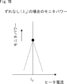
- 7A and 7B show examples of the spectrum and monitor power when the wavelength of the light source light SO1 output from the single-wavelength light source 110 does not deviate from the set wavelength ( ⁇ 0).
- the spectrum of the modulated optical signal SO2 generated by the semiconductor modulator 120 and the spectrum of the monitor optical signal SO4 branched from the splitter 130 are included in the transmission band spectrum of the band-pass optical filter 140.
- the bandwidth of the transmission band spectrum of the band-pass optical filter 140 corresponds to the bandwidth of the modulated optical signal SO2 output from the semiconductor modulator 120.
- the bandwidth of the transmission band of the band-pass optical filter 140 is wider than the bandwidth of the modulated optical signal SO2, or is approximately the same width as the bandwidth of the modulated optical signal SO2, and is at least a bandwidth that can transmit the modulated optical signal SO2. Then, as shown in FIG. 7B, when the wavelength of the light source light SO1 does not deviate from the set wavelength ( ⁇ 0), the monitor power (monitor current) of the monitor optical signal SO4 that has passed through the band-pass optical filter 140 becomes a maximum value. For example, the wavelength control unit 170 determines that wavelength control is unnecessary because the monitor power is greater than a predetermined threshold value (S103).
- FIG. 8A and 8B show examples of the spectrum and monitor power when the wavelength of the light source light SO1 output from the single-wavelength light source 110 is shifted to the shorter wavelength side than the set wavelength ( ⁇ 0).
- the spectrum of the modulated optical signal SO2 generated by the semiconductor modulator 120 and the monitor optical signal SO4 branched from the splitter 130 are shifted to the shorter wavelength side than the transmission band spectrum of the band-pass optical filter 140. Therefore, the short-wavelength side portion of the monitor optical signal SO4 that is not included in the transmission band is cut by the band-pass optical filter 140. Then, as shown in FIG.
- the monitor power (monitor current) of the monitor optical signal SO4 transmitted through the band-pass optical filter 140 becomes smaller than the maximum value.
- the wavelength control unit 170 determines that wavelength control is necessary because the monitor power is smaller than a predetermined threshold (S103), and controls the wavelength of the single-wavelength light source 110 (S104).
- the wavelength of the single-wavelength light source 110 is adjusted to the longer wavelength side by increasing the heater current according to the monitor power.
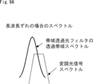
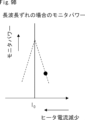
- FIG. 9A and 9B show examples of the spectrum and monitor power when the wavelength of the light source light SO1 output from the single-wavelength light source 110 is shifted to the long wavelength side from the set wavelength ( ⁇ 0).
- the spectrum of the modulated optical signal SO2 generated by the semiconductor modulator 120 and the monitor optical signal SO4 branched from the splitter 130 are shifted to the long wavelength side from the transmission band spectrum of the band-pass optical filter 140. Therefore, the long wavelength side portion of the monitor optical signal SO4 that is not included in the transmission band is cut by the band-pass optical filter 140. Then, as shown in FIG.
- the monitor power (monitor current) of the monitor optical signal SO4 transmitted through the band-pass optical filter 140 becomes smaller than the maximum value.
- the wavelength control unit 170 determines that wavelength control is necessary because the monitor power is smaller than a predetermined threshold (S103), and controls the wavelength of the single-wavelength light source 110 (S104).
- the wavelength of the single-wavelength light source 110 is adjusted to the shorter wavelength side by reducing the heater current according to the monitor power.
- the optical transmitter 1 determines in S103 that wavelength control is not necessary, or if the wavelength control in S104 is completed, it performs bias control processing of the semiconductor modulator 120 (S105 to S107).
- the monitor PD 150 monitors the light that has passed through the bandpass optical filter 140 (S105).
- the semiconductor modulator 120 modulates the wavelength-controlled light source light SO1
- the monitor PD 150 detects the optical signal that has passed through the bandpass optical filter 140 and converts the detected optical signal into a monitor current (monitor signal MO).
- the bias control unit 160 determines whether or not bias control (adjustment) of the semiconductor modulator 120 is necessary based on the monitoring result of the monitor PD 150 (S106). For example, the bias control unit 160 determines whether or not the monitor current (monitor signal MO) output from the monitor PD 150 is within a predetermined range, and if the monitor current exceeds the predetermined range, determines that bias control is necessary.
- the bias control unit 160 controls (adjusts) the bias voltage BS of the semiconductor modulator 120 (S107). Based on the detected monitor current, the bias control unit 160 controls the bias voltage BS1 applied to the MZ modulator 122-1, the bias voltage BS2 applied to the MZ modulator 122-2, and the bias voltage BS3 applied to the phase shifter 123. For example, the bias control unit 160 repeats the adjustment of the bias voltages BS1 to BS3 until the monitor current falls within a predetermined range.
- the optical transmitter 1 repeats the wavelength control process (S102 to S104) and the bias control process (S105 to S107) in order.
- the wavelength control process and the bias control process may be repeated constantly or periodically.
- the wavelength control process and the bias control process may be executed independently. That is, the wavelength control process and the bias control process may be executed in parallel, or may be executed in different cycles. Since the period from when the wavelength of the light source is adjusted until the wavelength shifts is longer than the period from when the bias voltage is adjusted until the bias point of the semiconductor modulator shifts, the bias control process may be executed in a first cycle, and the wavelength control process may be executed in a second cycle that is longer than the first cycle.
- an optical bandpass filter with a set wavelength as its center transmission wavelength is placed in front of the monitor PD.
- the light from the semiconductor modulator is branched by a coupler, and the branched light is input to the bandpass filter.
- the wavelength is controlled by identifying the electrical signal output from the monitor PD in the wavelength control unit and controlling the heater current of the light source, and then the electrical signal output from the monitor PD is identified and processed in the bias control unit to control the bias voltage of the optical modulator.
- FIG. 10 shows an example of the configuration of the optical transmitter 1 according to this embodiment.
- the optical transmitter 1 according to this embodiment includes an optical switch 180 in addition to the configuration of FIG. 3 of the first embodiment.
- the other configurations are the same as those of the first embodiment.
- the optical switch 180 is disposed between the splitter 130 and the bandpass optical filter 140, and is a switching unit that switches the bandpass optical filter 140 so that it can be bypassed. It can also be said that the optical switch 180 switches the presence or absence (use or non-use) of the bandpass optical filter 140.
- the optical switch 180 is formed on the semiconductor substrate 200, similar to the splitter 130, the bandpass optical filter 140, etc.
- the optical switch 180 switches the output destination of the monitor optical signal SO4 from the splitter 130, and outputs the monitor optical signal SO4 to either the bandpass optical filter 140 or the monitor PD 150. This switches whether or not to bypass the bandpass optical filter 140, i.e., whether or not to have the bandpass optical filter 140 filter the monitor optical signal SO4.
- the wavelength control unit 170 when the wavelength control unit 170 performs wavelength control processing, it connects the output of the splitter 130 to the input of the bandpass optical filter 140, and switches the output destination of the monitor optical signal SO4 to the bandpass optical filter 140. This causes the bandpass optical filter 140 to filter the monitor optical signal SO4, and the monitor optical signal SO4 that has passed through the bandpass optical filter 140 is detected by the monitor PD 150.
- the bias control unit 160 when the bias control unit 160 performs bias control processing, it connects the output of the splitter 130 to the input of the monitor PD 150, and switches the output destination of the monitor optical signal SO4 to the monitor PD 150. This bypasses the bandpass optical filter 140, and the monitor optical signal SO4 branched by the splitter 130 is directly detected by the monitor PD 150.
- the bandwidth of the transmission band of the band-pass optical filter 140 is narrower than that of the first embodiment.
- FIG. 11 shows an example of the transmission band spectrum of the band-pass optical filter 140. As shown in FIG. 11, for example, the bandwidth of the transmission band spectrum is narrower than the bandwidth of the modulated optical signal S02 output from the semiconductor modulator 120.
- the bandwidth of the transmission band of the band-pass optical filter 140 may correspond to the bandwidth of the light source light SO1 output from the single-wavelength light source 110.
- the bandwidth of the transmission band of the band-pass optical filter 140 may be wider than the bandwidth of the light source light SO1, or may be approximately the same as the bandwidth of the light source light SO1, and may be at least a bandwidth that can transmit the light source light SO1.
- FIG. 12 shows an example of the operation of the optical transmitter 1 according to this embodiment.
- S111 and S112 are added to the example of the operation of FIG. 6 of the first embodiment, and S105 is changed to S115.
- the optical transmitter 1 sets the initial values of the heater current HT of the single-wavelength light source 110 and the bias voltage BS of the semiconductor modulator 120 in the same manner as in the first embodiment (S101), and then switches the connection of the optical switch 180 to use the bandpass optical filter 140 in order to perform wavelength control processing (S111).
- the optical switch 180 directs the output of the monitor optical signal SO4 from the splitter 130 to the bandpass optical filter 140.
- the optical transmitter 1 performs wavelength control processing (S102 to S104) in the same manner as in the first embodiment.
- the bandpass optical filter 140 transmits the monitor optical signal SO4 from the optical switch 180 in a narrow transmission band as shown in FIG. 11.
- the monitor PD 150 monitors the optical signal that has passed through the bandpass optical filter 140, and the wavelength control unit 170 controls the wavelength of the single-wavelength light source 110 according to the monitoring result.
- the optical transmitter 1 switches the connection of the optical switch 180 to bypass the bandpass optical filter 140 in order to perform bias control processing (S112).
- the optical switch 180 directs the output of the monitor optical signal SO4 from the demultiplexer 130 to the monitor PD 150.
- the optical transmitter 1 performs bias control processing (S115, S106 to S107) in the same manner as in the first embodiment.
- the monitor PD 150 monitors the monitor optical signal SO4 from the optical switch 180 without passing through the bandpass optical filter 140 (S115).
- the bias control unit 160 controls the bias voltage BS of the semiconductor modulator 120 according to the monitoring result (S106 to S107).
- the transmission band of the bandpass filter is narrowed, and the presence or absence of a bandpass filter can be selected.
- the precision of wavelength control can be improved by monitoring the light that has passed through a bandpass filter with a narrow transmission band.
- bias control the influence of a bandpass filter with a narrow transmission band can be suppressed by bypassing the bandpass filter, enabling precise bias control.
- an optical transmitter includes a DP-IQ modulator as a semiconductor modulator.
- This embodiment can be implemented in combination with the first or second embodiment, and each configuration shown in the first or second embodiment may be used as appropriate.
- FIG. 13 shows an example of the configuration of the optical transmitter 1 according to this embodiment.
- FIG. 14 shows a specific example of the configuration of the DP-IQ modulator 220 in FIG. 13.
- the optical transmitter 1 according to this embodiment includes a DP-IQ modulator 220 as the semiconductor modulator 120 of embodiment 1.
- the other configurations are the same as those of embodiment 1.
- the DP-IQ modulator 220 is a DP (dual polarization) type IQ modulator, and is a semiconductor modulator formed on a semiconductor substrate 200. As shown in FIG. 14, the DP-IQ modulator 220 includes two IQ modulators that constitute the semiconductor modulator 120 of the first embodiment. One of the two IQ modulators is an IQ modulator for X-polarized waves, and the other is an IQ modulator for Y-polarized waves.
- the DP-IQ modulator 220 includes splitters 121-1 to 121-2, MZ modulators 122-1 to 122-4, phase shifters 123-1 to 123-2, multiplexers 124-1 to 124-2, splitter 125, polarization rotator 126, and polarization coupler 127.
- the splitter 125 splits (demultiplexes) the light source light SO1 from the single-wavelength light source 110 into light for X polarization and light for Y polarization.
- the splitter 121-1, the MZ modulators 122-1 to 122-2, the phase shifter 123-1, and the multiplexer 124-1 constitute, for example, an IQ modulator for X-polarized waves.
- the splitter 121-2, the MZ modulators 122-3 to 122-4, the phase shifter 123-2, and the multiplexer 124-2 constitute, for example, an IQ modulator for Y-polarized waves.
- the configurations of the IQ modulator for X-polarized waves and the IQ modulator for Y-polarized waves are similar to those of the semiconductor modulator 120 in the first embodiment.
- MZ modulator 122-1 is applied with a bias voltage BS1 and modulates the X-polarized Ich light branched by splitter 121-1 in accordance with data signal DT1.
- MZ modulator 122-2 is applied with a bias voltage BS2 and modulates the X-polarized Qch light branched by splitter 121-1 in accordance with data signal DT2.
- Phase shifter 123-1 is applied with a bias voltage BS3 and shifts the phase of the modulated optical signal for X-polarized Qch modulated by MZ modulator 122-2.
- MZ modulator 122-3 is applied with bias voltage BS4 and modulates the Y-polarized Ich light branched by splitter 121-2 in accordance with data signal DT3.
- MZ modulator 122-4 is applied with bias voltage BS5 and modulates the Y-polarized Qch light branched by splitter 121-2 in accordance with data signal DT4.
- Phase shifter 123-2 is applied with bias voltage BS6 and shifts the phase of the modulated optical signal for Y-polarized Qch modulated by MZ modulator 122-4.
- the polarization rotator 126 rotates the polarization direction of the modulated optical signal output from the IQ modulator for X polarization or the modulated optical signal output from the IQ modulator for Y polarization so that the polarization direction of the modulated optical signal output from the IQ modulator for X polarization is orthogonal to the polarization direction of the modulated optical signal output from the IQ modulator for Y polarization.
- the polarization rotator 126 rotates the polarization direction of the modulated optical signal output from the IQ modulator for X polarization (combiner 124-1) by 90°.
- the polarization coupler 127 polarization-couples the modulated optical signal of X-polarization, which has been output from the IQ modulator for X-polarization (combiner 124-1) and has its polarization direction rotated, and the modulated optical signal of Y-polarization, which has been output from the IQ modulator for Y-polarization (combiner 124-2), and outputs the polarization-coupled optical signal as modulated optical signal SO2.
- the splitter 130 splits the modulated optical signal SO2 including the X-polarized wave and the Y-polarized wave generated by the DP-IQ modulator 220 into an output optical signal SO3 for output and a monitor optical signal SO4 for monitoring.
- the bias control unit 160 controls the bias voltage BS of the DP-IQ modulator 220 based on the monitor signal MO that is transmitted through the bandpass optical filter 140 and monitored by the monitor PD 150.
- the bias control unit 160 controls the bias voltage BS1 of the MZ modulator 122-1, the bias voltage BS2 of the MZ modulator 122-2, the bias voltage BS3 of the phase shifter 123-1, the bias voltage BS4 of the MZ modulator 122-3, the bias voltage BS5 of the MZ modulator 122-4, and the bias voltage BS6 of the phase shifter 123-2 based on the monitor signal MO.
- the wavelength control unit 170 controls the wavelength of the single-wavelength light source 110 based on the monitor signal MO.
- the optical transmitter may include a DP-IQ modulator as a semiconductor modulator.
- the DP-IQ modulator and the like can be integrated to perform bias control and wavelength control appropriately.
- FIG. 15 shows an example of the configuration of the optical transmitter 1 according to this embodiment.
- the optical transmitter 1 according to this embodiment includes multiple DP-IP modulators 220-1 to 220-N (modulator array).
- the DP-IP modulators 220-1 to 220-N are the DP-IP modulators shown in embodiment 3.
- a single-wavelength light source 110, a splitter 111, DP-IP modulators 220-1 to 220-N, splitters 130-1 to 130-N, a bandpass optical filter 140, and monitor PDs 150-1 to 150-N are provided on a semiconductor substrate 200.
- the splitter 111 splits (demultiplexes) the light source light SO1 from the single-wavelength light source 110 to the DP-IP modulators 220-1 to 220-N.
- the DP-IP modulators 220-1 to 220-N each modulate the light split from the splitter 111.
- the splitters 130-1 to 130-N split the modulated optical signals generated by the DP-IP modulators 220-1 to 220-N into an output optical signal and a monitor optical signal.
- the bandpass optical filter 140 transmits the monitor optical signal branched by any of the splitters 130-1 to 130-N according to the transmission band.
- the bandpass optical filter 140 transmits the monitor optical signal generated by the DP-IP modulator 220-N and branched by the splitter 130-N.
- the bandpass optical filter 140 is not limited to the splitter 130-N, and may also transmit monitor optical signals branched by other splitters 130.
- Monitor PD 150-N monitors the optical signal that has passed through the bandpass optical filter 140.
- the other monitor PDs 150-1 to 150-N-1 monitor the monitor optical signals generated by the DP-IP modulators 220-1 to 220-N-1 and branched by the splitters 130-1 to 130-N-1, respectively.
- the bias control unit 160 controls the bias voltages BS of the DP-IP modulators 220-1 to 220-N, respectively, based on the monitor signals MO monitored by the monitor PDs 150-1 to 150-N. That is, the bias control unit 160 controls the bias voltages BS of the DP-IP modulators 220-1 to 220-N, respectively, based on the optical signals modulated by the DP-IP modulators 220-1 to 220-N and branched by the splitters 130-1 to 130-N.
- the bias control unit 160 controls the bias voltage BS of the DP-IP modulator 220-1 according to the monitoring results of the monitor PD 150-1, controls the bias voltage BS of the DP-IP modulator 220-2 according to the monitoring results of the monitor PD 150-2, ...
- the wavelength control unit 170 controls the bias voltage BS of the DP-IP modulator 220-N according to the monitoring results of the monitor PD 150-N.
- the wavelength control unit 170 controls the wavelength of the single-wavelength light source 110 based on the monitor signal MO monitored by the monitor PD 150-N. That is, the wavelength control unit 170 controls the wavelength of the single-wavelength light source 110 based on the optical signal modulated by one of the DP-IP modulators 220-1 to 220-N and branched by the branching filter 130.
- the optical transmitter may include multiple DP-IQ modulators as semiconductor modulators. Even in this case, similar to the first embodiment, multiple DP-IQ modulators etc. can be integrated to perform bias control and wavelength control appropriately.
- an optical transmitter includes a plurality of DP-IQ modulators and a multi-wavelength light source
- This embodiment can be implemented in combination with any of the first to fourth embodiments, and each configuration shown in any of the first to fourth embodiments may be used as appropriate.
- FIG. 16 shows an example of the configuration of the optical transmitter 1 according to this embodiment.
- the optical transmitter 1 according to this embodiment includes a multi-wavelength light source 112 instead of the single-wavelength light source 110, and a wavelength demultiplexer 113 instead of the demultiplexer 111, in comparison with the configuration of embodiment 4.
- the other configurations are the same as those of embodiment 4.
- the multi-wavelength light source 112 is a light source that outputs a multi-wavelength (multiple wavelengths) light source light SO1, and outputs light with wavelengths ⁇ 1 to ⁇ N.
- the multi-wavelength light source 112 outputs light with multiple wavelengths whose wavelength intervals are locked at equal intervals.
- the multi-wavelength light source 112 is, for example, a semiconductor laser such as a comb light source, and is formed on a semiconductor substrate 200.
- the wavelength demultiplexer 113 demultiplexes (branches) the light source light SO1 of multiple wavelengths output from the multi-wavelength light source 112 into individual wavelengths.
- the wavelength demultiplexer 113 is, for example, an AWG (Arrayed Waveguide Gratings), and is formed on a semiconductor substrate 200.
- the wavelength demultiplexer 113 outputs the optical signals of wavelengths ⁇ 1 to ⁇ N from the multi-wavelength light source 112 to the DP-IP modulators 220-1 to 220-N for each wavelength.
- the wavelength demultiplexer 113 outputs the optical signal of wavelength ⁇ 1 to DP-IP modulator 220-1, outputs the optical signal of wavelength ⁇ 2 to DP-IP modulator 220-2, ..., outputs the optical signal of wavelength ⁇ N to DP-IP modulator 220-N.
- the DP-IP modulators 220-1 to 220-N modulate the light of each wavelength branched from the wavelength branching filter 113, as in the fourth embodiment.
- the branching filters 130-1 to 130-N, the bandpass optical filter 140, the monitor PDs 150-1 to 150-N, and the bias control unit 160 are also the same as in the fourth embodiment.
- the bandpass optical filter 140 transmits the monitor optical signal generated by the DP-IP modulator 220-N and branched by the branching filter 130-N
- the transmission band of the bandpass optical filter 140 corresponds to the wavelength ( ⁇ N) of the optical signal modulated by the DP-IP modulator 220-N.
- the wavelength control unit 170 controls all of the multiple wavelengths of the multi-wavelength light source 112 based on the monitor signal MO monitored by the monitor PD 150-N. As in the first embodiment, the wavelength control unit 170 controls the multiple wavelengths by supplying a heater current to a heater formed in the multi-wavelength light source 112. Since the spacing between the multiple wavelengths is locked in the multi-wavelength light source 112, the multiple wavelengths can be controlled collectively by controlling the heater current according to the monitoring results of the optical signal modulated by one of the modulators.
- FIG. 17 shows another example of the configuration of the optical transmitter 1 according to this embodiment.
- the optical transmitter 1 includes a single-wavelength light source 110 and a multi-wavelength light source 114 as light sources.
- the single-wavelength light source 110 is a master laser
- the multi-wavelength light source 114 is a slave laser.
- the single-wavelength light source 110 and the multi-wavelength light source 114 are formed on a semiconductor substrate 200.
- the single-wavelength light source 110 outputs light of a single wavelength, as in the first embodiment.
- the multi-wavelength light source 114 outputs light of multiple wavelengths whose wavelength intervals are locked at equal intervals, as in the multi-wavelength light source 112 of FIG. 16.
- the wavelength of the multi-wavelength light source 114 is adjusted by injection locking with the light output from the single-wavelength light source 110.
- the wavelength control unit 170 supplies a heater current to a heater formed in the single-wavelength light source 110, as in the first embodiment, to control the wavelength of the single-wavelength light.
- the wavelength spacing of the multiple wavelengths is locked, so that by controlling the wavelength of the light input to the multi-wavelength light source 114, the wavelengths of the multiple wavelengths of light can be controlled collectively.
- the optical transmitter may include multiple DP-IQ modulators and a multi-wavelength light source. Even in this case, similar to the first embodiment, multiple DP-IQ modulators and a multi-wavelength light source, etc., can be integrated to perform bias control and wavelength control appropriately.
- a part or all of the above-described embodiments can be described as, but is not limited to, the following supplementary notes.
- Appendix 1 A light source generating a source light; a semiconductor modulator that modulates the generated light source light into modulated light; a splitter for splitting the modulated light into an output light and a monitor light; an optical filter that transmits light in a transmission band from the branched monitor light; an optical monitor for monitoring the transmitted light; a bias control means for controlling a bias voltage of the semiconductor modulator based on the monitoring result; a wavelength control means for controlling the wavelength of the light source light based on the monitoring result;
- An optical transmitter comprising: (Appendix 2)
- the transmission band of the optical filter is a band corresponding to a set wavelength set as the wavelength of the light source light output from the light source.
- the optical transmitter of claim 1 (Appendix 3) The set wavelength of the light source is variable; The transmission band of the optical filter is switched in response to a change in the set wavelength of the light source. 3.
- the optical transmitter of claim 2. (Appendix 4) The bandwidth of the transmission band corresponds to the bandwidth of the modulated light. 4.
- the optical transmitter of claim 2 or 3. (Appendix 5) The bandwidth of the transmission band is narrower than the bandwidth of the modulated light. 5.
- the optical transmitter of claim 4. (Appendix 6) The bandwidth of the transmission band corresponds to the bandwidth of the light source light. 6.
- the optical transmitter of claim 5. (Appendix 7) an optical switch for switching between the demultiplexer and the optical filter so as to be able to bypass the optical filter; 7.
- the optical transmitter according to claim 1 The optical transmitter according to claim 1 .
- the optical switch connects an output of the demultiplexer to an input of the optical monitor when the bias control means controls the bias voltage; 8.
- the optical transmitter of claim 7. the optical switch connects an output of the demultiplexer to an input of the optical filter when the wavelength control means controls the wavelength of the light from the light source.
- the optical transmitter of claim 7 or 8. After the wavelength control means controls the wavelength of the light source light, the bias control means controls the bias voltage.
- the optical transmitter according to claim 1 (Appendix 11) a heater capable of heating the light source; The wavelength control means controls the amount of heat generated by the heater in accordance with the monitored result. 11.
- the heater is formed in a region in a semiconductor substrate including the light source and the semiconductor modulator, the region corresponding to the light source.
- the optical transmitter of claim 11. (Appendix 13) The wavelength control means controls a drive current for driving the light source in accordance with the monitored result.
- the optical transmitter according to claim 1. (Appendix 14) an optical amplifier for adjusting the power of the light source light output from the light source; 14.
- the optical transmitter of claim 13. (Appendix 15)
- the semiconductor modulator comprises an IQ modulator including two MZ modulators. 15. The optical transmitter of claim 1 .
- the splitter splits the light output from the IQ modulator into the output light and the monitor light. 16. The optical transmitter of claim 15.
- the semiconductor modulator comprises a DP-IQ modulator including two of the IQ modulators. 17.
- the splitter splits the light output from the DP-IQ modulator into the output light and the monitor light. 18.
- the optical transmitter of claim 17. (Appendix 19)
- the semiconductor modulator comprises a plurality of the DP-IQ modulators. 19.
- the optical transmitter of claim 17 or 18. (Appendix 20)
- the optical filter transmits light modulated by any one of the plurality of DP-IQ modulators and branched by the demultiplexer. 20.
- the bias control means controls bias voltages of the plurality of DP-IQ modulators, respectively, based on the light modulated by the plurality of DP-IQ modulators and branched by the branching filter;
- the wavelength control means controls the wavelength of the light source light based on the light modulated by any one of the DP-IQ modulators and branched by the branching filter.
- the light source includes a multi-wavelength light source that generates a source light of multiple wavelengths, a wavelength demultiplexer that splits the generated multi-wavelength light source light into wavelengths and outputs the split lights to the plurality of DP-IQ modulators; 22.
- the wavelength control means controls all wavelengths of the multi-wavelength light source light.
- the optical transmitter of claim 22. the light source further comprises a single wavelength light source; the multi-wavelength light source generates the multi-wavelength light source light based on light output from the single-wavelength light source; The wavelength control means controls the wavelength of the light output from the single wavelength light source.
- the optical transmitter of claim 23. (Appendix 25) the light source, the semiconductor modulator, the splitter, the optical filter, and the optical monitor are formed on a single semiconductor substrate. 25. The optical transmitter of claim 1 .
- a light source generates a source light; modulating the generated light source light into modulated light by a semiconductor modulator; The modulated light is split into an output light and a monitor light, transmitting light in a transmission band from the branched monitor light; monitoring the transmitted light; Controlling the wavelength of the light source light based on the monitored result; controlling a bias voltage of the semiconductor modulator based on the monitored result; A method for controlling an optical transmitter.
- Appendix 27 When controlling the wavelength of the light source light, the wavelength of the light source light is controlled based on a result of monitoring the transmitted light; When controlling a bias voltage of the semiconductor modulator, the bias voltage of the semiconductor modulator is controlled based on a result of monitoring the branched monitor light.
- Optical transmitter 110 Single wavelength light source 111 Demultiplexer 112 Multi-wavelength light source 113 Wavelength demultiplexer 114 Multi-wavelength light source 120
- Semiconductor modulator 121 Demultiplexer 122, 122-1 to 122-4 MZ modulator 123, 123-1 to 123-2 Phase shifter 124, 124-1 to 124-2 Multiplexer 125
- Demultiplexer 126 Polarization rotator 127 Polarization coupler 130, 130-1 to 130-N Demultiplexer 140
- Optical switch 200 Semiconductor substrate 201 Lower cladding layer 202 Active layer 203 Upper cladding layer 204 Heater 205 Solder bump 220 DP-IQ modulator
Landscapes
- Physics & Mathematics (AREA)
- Nonlinear Science (AREA)
- General Physics & Mathematics (AREA)
- Optics & Photonics (AREA)
- Optical Modulation, Optical Deflection, Nonlinear Optics, Optical Demodulation, Optical Logic Elements (AREA)
Abstract
光送信器(1)は、光源光を生成する単一波長光源(110)と、生成した光源光を変調光に変調する半導体変調器(120)と、変調した変調光を出力光とモニタ光に分岐する分波器(130)と、分岐したモニタ光から透過帯域の光を透過する帯域透過光フィルタ(140)と、透過した光をモニタするモニタPD(150)と、モニタした結果に基づいて、半導体変調器(120)のバイアス電圧を制御するバイアス制御部(160)と、モニタした結果に基づいて、光源光の波長を制御する波長制御部(170)と、を備えるものである。
Description
本開示は、光送信器及び光送信器の制御方法に関する。
近年、インターネットや5G等の普及に伴い、基盤技術として利用される光通信において、高速化・大容量化の研究が進められている。例えば、光位相変調方式と偏波多重分離技術を組み合わせたデジタルコヒーレント方式を用いることで、100Gbps(Giga bit per second)超の大容量化が実現されている。このような高速伝送用の変調器として、MZ変調器(MZM:Mach-Zehnder Modulator)が利用されている。
関連する技術として、特許文献1~3が知られている。特許文献1には、MZ変調器を構成するLN(LiNbO3:ニオブ酸リチウム)変調器とLN変調器のバイアス電圧を制御する制御部が記載されている。さらに、特許文献2や3には、変調器に入力される光源の波長を制御する制御部も記載されている。
一方、半導体基板にMZ変調器を形成した半導体変調器の開発が進められており、今後、半導体変調器を含む光デバイスを集積化することにより、小型化及び省電力化が期待されている。しかしながら、関連する技術では、半導体変調器などの光デバイスを集積化することが考慮されていない。このため、関連する技術では、光送信器において変調器や光源を集積化する場合に、変調器のバイアス制御及び光源の波長制御を好適に行うことが困難となる可能性がある。
本開示は、このような課題に鑑み、変調器のバイアス制御及び光源の波長制御を好適に行うことが可能な光送信器及び光送信器の制御方法を提供することを目的とする。
本開示に係る光送信器は、光源光を生成する光源と、前記生成した光源光を変調光に変調する半導体変調器と、前記変調した変調光を出力光とモニタ光に分岐する分波器と、前記分岐したモニタ光から透過帯域の光を透過する光フィルタと、前記透過した光をモニタする光モニタと、前記モニタした結果に基づいて、前記半導体変調器のバイアス電圧を制御するバイアス制御手段と、前記モニタした結果に基づいて、前記光源光の波長を制御する波長制御手段と、を備えるものである。
本開示に係る光送信器の制御方法は、光源により光源光を生成し、前記生成した光源光を半導体変調器により変調光に変調し、前記変調した変調光を出力光とモニタ光に分岐し、前記分岐したモニタ光から透過帯域の光を透過し、前記透過した光をモニタし、前記モニタした結果に基づいて、前記光源光の波長を制御し、前記モニタした結果に基づいて、前記半導体変調器のバイアス電圧を制御するものである。
本開示によれば、変調器のバイアス制御及び光源の波長制御を好適に行うことが可能な光送信器及び光送信器の制御方法を提供することができる。
以下、図面を参照して実施の形態について説明する。各図面において、同一または対応する要素には同一の符号が付されており、説明の明確化のため、必要に応じて重複説明を省略する。なお、各図面において示された矢印は説明のための例示であり、信号の種類や方向を限定するものではない。
(関連する技術の検討)
まず、関連する技術について検討する。図1は、例えば特許文献1の記載に基づいた、関連する技術における光送信器9の構成を示している。図1は、LN変調器を用いた光送信器の構成例である。図1に示すように、関連する光送信器9は、光源901、LN変調器902、モニタPD903、バイアス制御部904を備えている。
まず、関連する技術について検討する。図1は、例えば特許文献1の記載に基づいた、関連する技術における光送信器9の構成を示している。図1は、LN変調器を用いた光送信器の構成例である。図1に示すように、関連する光送信器9は、光源901、LN変調器902、モニタPD903、バイアス制御部904を備えている。
光源901は、LN変調器902の外部に設けられた外付けの光源であり、LN変調器902と光ファイバ等を介して接続される。光源901は、例えばDFB(Distributed Feedback)レーザである。LN変調器902は、光源901から出力された光を変調する。モニタPD903は、LN変調器902の外部に設けられた受光部である。LN変調器902により変調された光をモニタPD903で受光しモニタする。バイアス制御部904は、モニタPD903のモニタ結果に応じて、LN変調器902のバイアス点(動作点)振動による出力ずれが小さくなるように、LN変調器902のバイアス電圧をフィードバック制御する。
また、光源から出力される光は、経年劣化等により波長が変動するため、光源から所望の波長の光が出力されるよう波長制御を行う必要がある。関連する技術として、温度調整機能を利用した波長制御方法が考えられる。図2は、関連する技術における光源の温度調整機能の配置例を示す概略側面図である。図2に示すように、関連する技術では、温度調整機能としてTEC(Thermoelectric Cooler)905を、外付けの光源901の下に配置する。TEC905により光源901下部の全面の温度を調整することで、光源901の波長を制御する。
しかし、関連する光送信器では、LN変調器に対し光源が外付けであり、光源の温度調整機能が大きいため、小型化の障害となる。また、LN変調器を半導体変調器として、半導体変調器と光源を集積化しようとすると、TECのような大きな温度調整機能では、局所的に光源の波長制御することは困難である。そこで、実施の形態では、光源の波長制御と半導体変調器のバイアス制御を近接して省面積で行うことを可能とする。
なお、特許文献2に記載の光角度変調器では、光源の光を2つに分岐し、分岐した光をそれぞれ光位相変調部と光周波数シフタに入力し、光位相変調部と光周波数シフタの出力光を結合する。この構成において、歪成分制御部が、結合された光信号に基づいて光位相変調部に印加するバイアス電圧を制御し、光源制御部が、光周波数シフタからの光信号に基づいて光源の波長を制御する。特許文献2では、光位相変調部から出力される光信号に基づいて、バイアス電圧と光源の波長を制御することはできないため、小型化することは困難である。
また、特許文献3に記載の光送信器では、LN変調器から出力される光信号をバンドパスフィルタに入力し、バンドパスフィルタを介した光信号を光カプラで分岐し、分岐した光に基づいて、LN変調器のバイアス電圧と光源の波長を制御する。特許文献3では、LN変調器を前提としているため、変調器及び光源等を集積化することはできない。また、バンドパスフィルタを介した光信号を光伝送路へ出力するため、光源の波長が大きく変動すると断信号となる場合があり、変動量によっては出力光のパワー低下につながる可能性がある。
(実施の形態1)
次に、実施の形態1について説明する。図3は、本実施の形態に係る光送信器1の構成例を示している。図4A及び図4Bは、図3の半導体基板200の各部の配置例を示す概略側面図である。図5は、図3の半導体変調器120の具体的な構成例を示している。
次に、実施の形態1について説明する。図3は、本実施の形態に係る光送信器1の構成例を示している。図4A及び図4Bは、図3の半導体基板200の各部の配置例を示す概略側面図である。図5は、図3の半導体変調器120の具体的な構成例を示している。
本実施の形態に係る光送信器1は、例えば、デジタルコヒーレント通信用の光送信器である。図3に示すように、光送信器1は、単一波長光源110、半導体変調器120、分波器130、帯域透過光フィルタ140、モニタPD150、バイアス制御部160、波長制御部170を備えている。
例えば、単一波長光源110、半導体変調器120、分波器130、帯域透過光フィルタ140、モニタPD150は、1つの半導体基板200上に形成されている。少なくとも単一波長光源110と半導体変調器120を半導体基板200上に形成してもよい。半導体基板200は、例えば、インジウムリン(InP)、ガリウムひ素(GaAs)やシリコン(Si)等の半導体基板であるが、ゲルマニウム(Ge)等のその他の半導体基板でもよい。
バイアス制御部160及び波長制御部170は、半導体基板200とは別の半導体チップとして形成されている。バイアス制御部160及び波長制御部170は、別々の半導体チップにより構成されてもよいし、1つの半導体チップにより構成されてもよい。バイアス制御部160及び波長制御部170は、ハードウェア又はソフトウェア、もしくはその両方によって構成されてもよい。バイアス制御部160及び波長制御部170の機能は、CPU(Central Processing Unit)等のプロセッサにおいて、メモリに格納されたプログラムを実行することにより実装してもよい。例えば、半導体基板200に、バイアス制御部160及び波長制御部170を含む半導体チップをフリップチップ等により実装してもよい。図3の全ての構成を含む半導体装置を1つの半導体パッケージとしてもよい。
単一波長光源110は、予め設定された単一波長(設定波長)の光である光源光SO1を生成する。単一波長光源110は、インジウムリンやシリコン等の半導体基板200に形成された半導体レーザである。単一波長光源110は、例えば、DFBレーザやDBR(Distributed Bragg Reflector)レーザでもよいし、外部共振型レーザ(External Cavity Laser: ECL)でもよい。単一波長光源110は、光源光SO1の設定波長が固定された波長固定光源であるが、光源光SO1の設定波長が可変の波長可変光源でもよい。
図4Aは、単一波長光源110を半導体基板200に実装する一例を示している。図4Aに示すように、単一波長光源110は、例えば、半導体基板200上に、下部クラッド層201、活性層202、上部クラッド層203が積層されて構成される。また、単一波長光源110(半導体基板200)の最上位、すなわち、上部クラッド層203の上にヒータ204が形成されている。ヒータ204は、単一波長光源110を加熱可能な発熱体である。ヒータ204は、TiNヒータ等の温度制御可能な抵抗体により形成されている。ヒータ204は、半導体基板200における単一波長光源110の形成領域に対応して形成されている。例えば、ヒータ204は、単一波長光源110の形成領域の範囲内に形成されてもよい。ヒータ204は、平面視で単一波長光源110の形成領域(活性層202)と同じ形状及びサイズでもよいし、単一波長光源110の形成領域より小さい形状及びサイズでもよい。ヒータ204は、単一波長光源110の形成領域より大きくてもよいが、半導体変調器120等の他の光デバイスの形成領域と重ならないことが好ましい。波長制御部170から供給されるヒータ電流HTに応じてヒータ204が発熱し、ヒータ204の熱により活性層202の屈折率が変化することで、活性層202で生じる光源光SO1の波長が制御される。活性層202の温度が調整できればよいため、ヒータ204は、上部クラッド層203の上に限らず、上部クラッド層203の中でもよいし、下部クラッド層201の下や半導体基板200の下に形成されてもよい。例えば、単一波長光源110が外部共振型レーザである場合、外部共振型レーザを構成するシリコン導波路にヒータを形成し、形成したヒータの熱によりシリコン導波路の屈折率を調整することで波長を制御してもよい。
図4Bは、単一波長光源110を半導体基板200に実装する他の例を示している。図4Bに示すように、単一波長光源110の半導体チップを半導体基板200にフリップチップ実装してもよい。すなわち、図4Aのように単一波長光源110を半導体基板200に対しモノリシックに実装してもよいし、図4Bのように単一波長光源110を半導体基板200に対しハイブリッドに実装してもよい。図4Bの例では、単一波長光源110に形成されたヒータ204(図4Bでは最下位)と半導体基板200との間をはんだバンプ205を介して接合することで、単一波長光源110を半導体基板200に実装する。
図4Bは、単一波長光源110を半導体基板200に実装する他の例を示している。図4Bに示すように、単一波長光源110の半導体チップを半導体基板200にフリップチップ実装してもよい。すなわち、図4Aのように単一波長光源110を半導体基板200に対しモノリシックに実装してもよいし、図4Bのように単一波長光源110を半導体基板200に対しハイブリッドに実装してもよい。図4Bの例では、単一波長光源110に形成されたヒータ204(図4Bでは最下位)と半導体基板200との間をはんだバンプ205を介して接合することで、単一波長光源110を半導体基板200に実装する。
半導体変調器120は、デジタルコヒーレント通信用のIQ変調器である。半導体変調器120は、インジウムリンやシリコン等の半導体基板200に形成された半導体変調器である。半導体変調器120は、単一波長光源110から出力された光源光SO1を変調光信号SOに変調する。半導体変調器120は、単一波長光源110から出力された光源光SO1に対し、IQ変調(コヒーレント変調)をかけ、変調した変調光信号SO2を出力する。
図5に示すように、半導体変調器120は、2つのMZ変調器を含むMZ干渉系により構成される。半導体変調器120は、分波器121、MZ変調器122-1及び122-2、位相シフタ123、合波器124を備える。分波器121は、単一波長光源110からの光源光SO1をIch(同相成分)用の光とQch(直交成分)用の光に分岐(分波)する。
MZ変調器122-1は、例えば、Ich用の変調器である。MZ変調器122-1は、送信データ信号から生成されたIch用のデータ信号DT1が駆動信号として印加される。MZ変調器122-1は、分波器121により分岐されたIch用の光を、データ信号DT1に応じて変調する。また、MZ変調器122-1には、バイアス制御部160からバイアス点を調整するバイアス電圧BS1が印加される。
MZ変調器122-2は、例えば、Qch用の変調器である。MZ変調器122-2は、送信データ信号から生成されたQch用のデータ信号DT2が駆動信号として印加される。MZ変調器122-2は、分波器121により分岐されたQch用の光を、データ信号DT2に応じて変調する。また、MZ変調器122-2には、バイアス制御部160からバイアス点を調整するバイアス電圧BS2が印加される。
位相シフタ123は、Ichの光信号の位相とQchの光信号の位相が直交するように、Ichの光信号の位相またはQchの光信号の位相をシフトする。この例では、位相シフタ123は、MZ変調器122-2により変調されたQchの変調光信号の位相をπ/2シフトさせる。位相シフタ123は、MZ変調器と同様にMZ干渉計により構成してもよいし、導波路の屈折率を変えることで位相をシフトするように構成してもよい。また、位相シフタ123には、バイアス制御部160から位相シフト量を調整するバイアス電圧BS3が印加される。位相シフタ123をMZ干渉計により構成する場合、MZ干渉計に印加するバイアス電圧BS3により位相シフト量を制御してもよい。位相シフタ123を構成する導波路にヒータを形成し、形成したヒータにバイアス電圧BS3を印加して発生する熱により導波路の屈折率を変えることで、位相シフト量を制御してもよい。
合波器124は、MZ変調器122-1により変調された光信号と、MZ変調器122-2により変調され位相シフタ123により位相シフトされた光信号とを合波し、合波した変調光信号SO2を出力する。
分波器130は、半導体変調器120(IQ変調器)により生成された変調光信号SO2を、出力用の出力光信号SO3とモニタ用のモニタ光信号SO4に分岐する。分岐した出力光信号SO3は送信光として外部(光伝送路等)へ出力される。なお、半導体変調器120の合波器124と分波器130を1つの光カプラ(2×2光カプラ)としてもよい。
帯域透過光フィルタ140は、所定の透過帯域の光信号を透過する光BPF(Band Pass Filter)である。帯域透過光フィルタ140は、分波器130により分岐されたモニタ光信号SO4を入力し、モニタ光信号SO4のうち透過帯域の光を透過する。帯域透過光フィルタ140は、インジウムリンやシリコン等の半導体基板200に形成された半導体フィルタである。帯域透過光フィルタ140は、例えば、非対称MZ干渉計により構成される。帯域透過光フィルタ140は、リング共振器により構成してもよいし、対向するミラーを用いた共振器により構成してもよい。
帯域透過光フィルタ140の透過帯域は、単一波長光源110から出力される光源光SO1の設定波長(所望の目標波長)に対応する。単一波長光源110が波長可変光源の場合、帯域透過光フィルタ140を帯域可変フィルタとし、光源光SO1の設定波長の変更に応じて帯域透過光フィルタ140透過帯域を切り替えてもよい。帯域透過光フィルタ140を共振器により構成する場合、共振器の導波路にヒータを形成し、形成したヒータの熱を調整することで、帯域透過光フィルタの透過帯域を制御してもよい。また、透過帯域が異なる複数の帯域透過光フィルタを備え、単一波長光源110の光源光SO1の設定波長に応じて、使用する帯域透過光フィルタを切り替えてもよい。
モニタPD150は、帯域透過光フィルタ140を透過した光信号をモニタ(検出)するPD(Photo Detector)である。モニタPD150は、インジウムリン、シリコン等の半導体基板200に形成された半導体PDである。モニタPD150は、帯域透過光フィルタ140を透過した光信号を光電変換し、光電変化されたモニタ信号MOを出力する。
バイアス制御部160は、モニタPD150のモニタ結果であるモニタ信号MOに基づいて、半導体変調器120のバイアス電圧BSを制御する。半導体変調器120から出力された変調光を分岐し、分岐した光のモニタ結果に応じて、半導体変調器120のバイアス電圧をフィードバック制御することで、自動的にバイアス電圧を最適化する。この例では、バイアス制御部160は、モニタ信号MOに基づいて、MZ変調器122-1に印加するバイアス電圧BS1、MZ変調器122-2に印加するバイアス電圧BS2、位相シフタ123に印加するバイアス電圧BS3をそれぞれ制御する。
波長制御部170は、モニタPD150のモニタ結果であるモニタ信号MOに基づいて、単一波長光源110の光源光SO1の波長を制御する。波長制御部170は、モニタPD150のモニタ結果に応じて、ヒータ204の発熱量を制御する。波長制御部170は、モニタ信号MOに応じてヒータ電流HTを生成し、生成したヒータ電流HTを単一波長光源110に供給する。例えば、ヒータ電流HTを抵抗に流し、抵抗を介してヒータ電流HTに応じた電圧をヒータ204に印加して、ヒータ204に熱を発生させることで、単一波長光源110の光源光SO1の波長を制御する。なお、波長制御部170は、単一波長光源110を駆動する駆動電流を制御することで、光源光SO1の波長を調整してもよい。すなわち、波長制御部170は、モニタPD150のモニタ結果に応じて、単一波長光源110を駆動する駆動電流を制御してもよい。その場合、単一波長光源110が出力する光源光SO1のパワーが変化するため、光源光SO1のパワーを調整する光アンプを備えてもよい。
図6は、本実施の形態に係る光送信器1の動作例を示している。図6に示すように、まず、光送信器1は、単一波長光源110のヒータ電流HT及び半導体変調器120のバイアス電圧BSの初期値を設定する(S101)。波長制御部170は、予め決められた初期値のヒータ電流HTを生成し、生成したヒータ電流HTを単一波長光源110に供給する。具体的には、波長制御部170は、抵抗を介して、初期値のヒータ電流HTに応じた電圧をヒータ204に印加する。単一波長光源110は、初期値のヒータ電流HTにより設定された波長の光源光SO1を生成する。
また、バイアス制御部160は、予め決められた初期値のバイアス電圧BSを生成し、生成したバイアス電圧BSを半導体変調器120に供給する。具体的には、バイアス制御部160は、初期値のバイアス電圧BS1をMZ変調器122-1に印加し、初期値のバイアス電圧BS2をMZ変調器122-2に印加し、初期値のバイアス電圧BS3を位相シフタ123に印加する。半導体変調器120は、初期値のバイアス電圧BSにより設定されたバイアス点で変調動作を行う。
続いて、光送信器1は、単一波長光源110の波長制御処理を行う(S102~S104)。波長制御処理では、モニタPD150は、帯域透過光フィルタ140を介した光をモニタする(S102)。具体的には、半導体変調器120は、単一波長光源110から光源光SO1が入力され、データ信号DTが入力されると、光源光SO1をデータ信号DT1に応じて変調し、変調した変調光信号SO2を出力する。分波器130は、生成された変調光信号SO2を出力光信号SO3とモニタ光信号SO4に分岐する。帯域透過光フィルタ140は、分岐されたモニタ光信号SO4から透過帯域の光を透過する。モニタPD150は、帯域透過光フィルタ140を介した光信号を検出し、検出した光信号をモニタ電流(モニタ信号MO)に変換する。
続いて、波長制御部170は、モニタPD150のモニタ結果に基づいて、単一波長光源110の波長制御(調整)が必要か否か判定する(S103)。例えば、波長制御部170は、モニタPD150から出力されたモニタ電流(モニタ信号MO)が所定の閾値以下か否か判定し、モニタ電流が所定の閾値以下である場合、波長制御が必要であると判断する。
続いて、波長制御が必要であると判定された場合、波長制御部170は、単一波長光源110の波長を制御(調整)する(S104)。波長制御部170は、検出したモニタ電流に応じてヒータ電流HTを調整し、調整したヒータ電流HTを単一波長光源110に供給する。例えば、波長制御部170は、モニタ電流が所定の閾値を超えるまで、ヒータ電流HTの調整を繰り返す。
図7A及び図7B~図9A及び図9Bは、単一波長光源110の波長制御の具体例を示している。図7A及び図7Bは、単一波長光源110から出力された光源光SO1の波長が設定波長(λ0)からずれていない場合のスペクトル及びモニタパワーの例を示している。この場合、図7Aに示すように、半導体変調器120が生成した変調光信号SO2及び分波器130から分岐したモニタ光信号SO4のスペクトルは、帯域透過光フィルタ140の透過帯域スペクトルに含まれる。帯域透過光フィルタ140の透過帯域スペクトルの帯域幅は、半導体変調器120から出力される変調光信号SO2の帯域幅に対応する。例えば、帯域透過光フィルタ140の透過帯域の帯域幅は、変調光信号SO2の帯域幅より広い、あるいは、変調光信号SO2の帯域幅とほぼ同じ幅であり、少なくとも変調光信号SO2を透過可能な帯域幅である。そうすると、図7Bに示すように、光源光SO1の波長が設定波長(λ0)からずれていない場合、帯域透過光フィルタ140を透過したモニタ光信号SO4のモニタパワー(モニタ電流)は最大値となる。例えば、波長制御部170は、モニタパワーが所定の閾値よりも大きいため、波長制御は不要であると判定する(S103)。
図8A及び図8Bは、単一波長光源110から出力された光源光SO1の波長が設定波長(λ0)より短波長側にずれている場合のスペクトル及びモニタパワーの例を示している。この場合、図8Aに示すように、半導体変調器120が生成した変調光信号SO2及び分波器130から分岐したモニタ光信号SO4のスペクトルは、帯域透過光フィルタ140の透過帯域スペクトルよりも短波長側にずれてしまう。このため、モニタ光信号SO4のうち透過帯域に含まれない短波長側の部分が帯域透過光フィルタ140でカットされる。そうすると、図8Bに示すように、光源光SO1の波長が設定波長(λ0)より短波長側にずれている場合、帯域透過光フィルタ140を透過したモニタ光信号SO4のモニタパワー(モニタ電流)は、最大値よりも小さくなる。例えば、波長制御部170は、モニタパワーが所定の閾値よりも小さいため、波長制御が必要であると判定し(S103)、単一波長光源110の波長を制御する(S104)。この例では、モニタパワーに応じてヒータ電流を増加させることで、単一波長光源110の波長を長波長側へ調整する。
図9A及び図9Bは、単一波長光源110から出力された光源光SO1の波長が設定波長(λ0)より長波長側にずれている場合のスペクトル及びモニタパワーの例を示している。この場合、図9Aに示すように、半導体変調器120が生成した変調光信号SO2及び分波器130から分岐したモニタ光信号SO4のスペクトルは、帯域透過光フィルタ140の透過帯域スペクトルよりも長波長側にずれてしまう。このため、モニタ光信号SO4のうち透過帯域に含まれない長波長側の部分が帯域透過光フィルタ140でカットされる。そうすると、図9Bに示すように、光源光SO1の波長が設定波長(λ0)より長波長側にずれている場合、帯域透過光フィルタ140を透過したモニタ光信号SO4のモニタパワー(モニタ電流)は、最大値よりも小さくなる。例えば、波長制御部170は、モニタパワーが所定の閾値よりも小さいため、波長制御が必要であると判定し(S103)、単一波長光源110の波長を制御する(S104)。この例では、モニタパワーに応じてヒータ電流を減少させることで、単一波長光源110の波長を短波長側へ調整する。
続いて、図6に示すように、光送信器1は、S103で波長制御が不要と判定された場合、または、S104の波長制御が終了した場合、半導体変調器120のバイアス制御処理を行う(S105~S107)。バイアス制御処理では、モニタPD150は、帯域透過光フィルタ140を介した光をモニタする(S105)。S102と同様に、半導体変調器120は、波長制御された光源光SO1を変調し、モニタPD150は、帯域透過光フィルタ140を介した光信号を検出し、検出した光信号をモニタ電流(モニタ信号MO)に変換する。
続いて、バイアス制御部160は、モニタPD150のモニタ結果に基づいて、半導体変調器120のバイアス制御(調整)が必要か否か判定する(S106)。例えば、バイアス制御部160は、モニタPD150から出力されたモニタ電流(モニタ信号MO)が所定の範囲内か否か判定し、モニタ電流が所定の範囲を超えている場合、バイアス制御が必要であると判断する。
続いて、バイアス制御が必要であると判定された場合、バイアス制御部160は、半導体変調器120のバイアス電圧BSを制御(調整)する(S107)。バイアス制御部160は、検出したモニタ電流に基づいて、MZ変調器122-1に印加するバイアス電圧BS1、MZ変調器122-2に印加するバイアス電圧BS2、位相シフタ123に印加するバイアス電圧BS3をそれぞれ制御する。例えば、バイアス制御部160は、モニタ電流が所定の範囲内となるまで、バイアス電圧BS1~BS3の調整を繰り返す。
その後、光送信器1は、波長制御処理(S102~S104)とバイアス制御処理(S105~S107)を順に繰り返す。波長制御処理及びバイアス制御処理を常に繰り返してもよいし、定期的に繰り返してもよい。一度、波長制御処理により単一波長光源110の波長が調整された後は、波長制御処理とバイアス制御処理をそれぞれ独立して実行してもよい。すなわち、波長制御処理とバイアス制御処理を並列に行ってもよいし、それぞれ異なる周期で行ってもよい。バイアス電圧を調整してから半導体変調器のバイアス点がずれるまでの期間よりも光源の波長を調整してから波長がずれるまでの期間の方が長いため、バイアス制御処理を第1の周期で行い、波長制御処理を第1の周期よりも長い第2の周期で行ってもよい。
以上のように、本実施の形態では、DFBレーザや波長可変光源などの単一波長光源と半導体変調器が同一基板上に集積された光送信器において、モニタPDの前段に設定波長を中心透過波長とする光バンドパスフィルタが配置されている。また、半導体変調器からの光をカプラで分岐し、分岐した光をバンドパスフィルタに入力する。波長制御及びバイアス制御では、モニタPDから出力された電気信号を用いて波長制御部で識別して光源のヒータ電流を制御することで波長制御し、その後、モニタPDから出力された電気信号を用いてバイアス制御部で識別処理して光変調器のバイアス電圧を制御する。
これにより、半導体変調器及び光源等を集積化するとともに、バイアス制御及び波長制御を好適に行うことができる。具体的には、半導体変調器及び光源等を同一の半導体基板に集積化することで、小型化及び省電力化することができる。バンドパスフィルタを介した光をモニタし、モニタ結果に基づいてバイアス制御及び波長制御を行うことで、1つのモニタPDでバイアス制御及び波長制御を行うことができる。モニタ結果に応じたヒータ電流により光源に形成されたヒータの熱を制御することで、TECなどの大型の温度調整機能を利用することなく光源の波長を制御できるため、光源の波長制御と半導体変調器のバイアス制御を近接して省面積で行うことができる。また、半導体変調器からの光を分岐し、分岐した光をモニタすることで、光伝送路などの外部へ出力される光への影響を抑えつつ、波長制御とバイアス制御を行うことができる。
(実施の形態2)
次に、実施の形態2について説明する。本実施の形態では、帯域透過光フィルタの透過帯域幅を狭くし、帯域透過光フィルタの有無を切り替え可能とする例について説明する。なお、本実施の形態は、実施の形態1と組み合わせて実施することが可能であり、実施の形態1で示した各構成を適宜使用してもよい。
次に、実施の形態2について説明する。本実施の形態では、帯域透過光フィルタの透過帯域幅を狭くし、帯域透過光フィルタの有無を切り替え可能とする例について説明する。なお、本実施の形態は、実施の形態1と組み合わせて実施することが可能であり、実施の形態1で示した各構成を適宜使用してもよい。
図10は、本実施の形態に係る光送信器1の構成例を示している。図10に示すように、本実施の形態に係る光送信器1は、実施の形態1の図3の構成に加えて、光スイッチ180を備えている。その他の構成は、実施の形態1と同様である。
光スイッチ180は、分波器130と帯域透過光フィルタ140の間に配置され、帯域透過光フィルタ140をバイパス可能に切り替える切り替え部である。光スイッチ180は、帯域透過光フィルタ140の有無(使用の有無)を切り替えるとも言える。光スイッチ180は、分波器130、帯域透過光フィルタ140等と同様に、半導体基板200上に形成されている。光スイッチ180は、分波器130からのモニタ光信号SO4の出力先を切り替え、モニタ光信号SO4を帯域透過光フィルタ140とモニタPD150のいずれかに出力する。これにより、帯域透過光フィルタ140をバイパスするか否か、すなわち、帯域透過光フィルタ140にモニタ光信号SO4をフィルタリングさせるか否か切り替える。
例えば、波長制御部170が波長制御処理を行う場合、分波器130の出力を帯域透過光フィルタ140の入力に接続し、モニタ光信号SO4の出力先を帯域透過光フィルタ140に切り替える。これにより、帯域透過光フィルタ140にモニタ光信号SO4をフィルタリングさせ、帯域透過光フィルタ140を透過したモニタ光信号SO4をモニタPD150で検出する。また、バイアス制御部160がバイアス制御処理を行う場合、分波器130の出力をモニタPD150の入力に接続し、モニタ光信号SO4の出力先をモニタPD150に切り替える。これにより、帯域透過光フィルタ140をバイパスし、分波器130で分岐したモニタ光信号SO4を直接モニタPD150で検出する。
また、本実施の形態では、帯域透過光フィルタ140の透過帯域の帯域幅を実施の形態1よりも狭くする。図11は、帯域透過光フィルタ140の透過帯域スペクトルの例を示している。図11に示すように、例えば、透過帯域スペクトルの帯域幅は、半導体変調器120から出力される変調光信号S02の帯域幅よりも狭い。帯域透過光フィルタ140の透過帯域の帯域幅は、単一波長光源110から出力される光源光SO1の帯域幅に対応してもよい。帯域透過光フィルタ140の透過帯域の帯域幅は、光源光SO1の帯域幅より広い、あるいは、光源光SO1の帯域幅とほぼ同じ幅であり、少なくとも光源光SO1を透過可能な帯域幅でもよい。
図12は、本実施の形態に係る光送信器1の動作例を示している。この例では、実施の形態1の図6の動作例に対し、S111及びS112が追加され、S105がS115に変更されている。
図12に示すように、光送信器1は、実施の形態1と同様に単一波長光源110のヒータ電流HT及び半導体変調器120のバイアス電圧BSの初期値を設定した後(S101)、波長制御処理を行うため、帯域透過光フィルタ140を使用するよう光スイッチ180の接続を切り替える(S111)。光スイッチ180は、分波器130からのモニタ光信号SO4の出力先を帯域透過光フィルタ140とする。
続いて、光送信器1は、実施の形態1と同様に、波長制御処理(S102~S104)を行う。帯域透過光フィルタ140は、光スイッチ180からのモニタ光信号SO4を、図11のように狭い透過帯域で透過する。モニタPD150は、帯域透過光フィルタ140を透過した光信号をモニタし、波長制御部170は、そのモニタ結果に応じて、単一波長光源110の波長を制御する。
続いて、光送信器1は、バイアス制御処理を行うため、帯域透過光フィルタ140をバイパスするよう光スイッチ180の接続を切り替える(S112)。光スイッチ180は、分波器130からのモニタ光信号SO4の出力先をモニタPD150とする。
続いて、光送信器1は、実施の形態1と同様に、バイアス制御処理(S115、S106~S107)を行う。モニタPD150は、帯域透過光フィルタ140を介さずに、光スイッチ180からのモニタ光信号SO4をモニタする(S115)。バイアス制御部160は、そのモニタ結果に応じて、半導体変調器120のバイアス電圧BSを制御する(S106~S107)。
以上のように、本実施の形態では、バンドパスフィルタの透過帯域を狭くし、バンドパスフィルタの有無を選択可能とする。波長制御を行う場合に、狭い透過帯域のバンドパスフィルタを透過した光をモニタすることで、波長制御の精度を向上できる。また、バイアス制御を行う場合は、バンドパスフィルタをバイパスすることで、狭い透過帯域のバンドパスフィルタによる影響を抑え、精度よくバイアス制御を行うことができる。
(実施の形態3)
次に、実施の形態3について説明する。本実施の形態では、光送信器が半導体変調器としてDP-IQ変調器を備える例について説明する。なお、本実施の形態は、実施の形態1または2と組み合わせて実施することが可能であり、実施の形態1または2で示した各構成を適宜使用してもよい。
次に、実施の形態3について説明する。本実施の形態では、光送信器が半導体変調器としてDP-IQ変調器を備える例について説明する。なお、本実施の形態は、実施の形態1または2と組み合わせて実施することが可能であり、実施の形態1または2で示した各構成を適宜使用してもよい。
図13は、本実施の形態に係る光送信器1の構成例を示している。図14は、図13のDP-IQ変調器220の具体的な構成例を示している。図13に示すように、本実施の形態に係る光送信器1では、実施の形態1の半導体変調器120として、DP-IQ変調器220を備えている。その他の構成は、実施の形態1と同様である。
DP-IQ変調器220は、DP(dual polarization)型のIQ変調器であり、半導体基板200上に形成された半導体変調器である。図14に示すように、DP-IQ変調器220は、実施の形態1の半導体変調器120を構成するIQ変調器を2つ備えている。2つのIQ変調器のうち一方がX偏波用のIQ変調器であり、他方がY偏波用のIQ変調器である。
具体的には、DP-IQ変調器220は、分波器121-1~121-2、MZ変調器122-1~122-4、位相シフタ123-1~123-2、合波器124-1~124-2、分波器125、偏波回転器126、偏波結合器127を備える。分波器125は、単一波長光源110からの光源光SO1をX偏波用の光とY偏波用の光に分岐(分波)する。
分波器121-1、MZ変調器122-1~122-2、位相シフタ123-1、合波器124-1は、例えば、X偏波用のIQ変調器を構成する。分波器121-2、MZ変調器122-3~122-4、位相シフタ123-2、合波器124-2は、例えば、Y偏波用のIQ変調器を構成する。X偏波用のIQ変調器とY偏波用のIQ変調器の各構成は、実施の形態1の半導体変調器120と同様である。
MZ変調器122-1は、バイアス電圧BS1が印加され、分波器121-1により分岐されたX偏波のIch用の光を、データ信号DT1に応じて変調する。MZ変調器122-2は、バイアス電圧BS2が印加され、分波器121-1により分岐されたX偏波のQch用の光を、データ信号DT2に応じて変調する。位相シフタ123-1は、バイアス電圧BS3が印加され、MZ変調器122-2により変調されたX偏波のQch用の変調光信号の位相をシフトさせる。
MZ変調器122-3は、バイアス電圧BS4が印加され、分波器121-2により分岐されたY偏波のIch用の光を、データ信号DT3に応じて変調する。MZ変調器122-4は、バイアス電圧BS5が印加され、分波器121-2により分岐されたY偏波のQch用の光を、データ信号DT4に応じて変調する。位相シフタ123-2は、バイアス電圧BS6が印加され、MZ変調器122-4により変調されたY偏波のQch用の変調光信号の位相をシフトさせる。
偏波回転器126は、X偏波用のIQ変調器から出力された変調光信号の偏波方向と、Y偏波用のIQ変調器から出力された変調光信号の偏波方向が直交するように、X偏波用のIQ変調器から出力された変調光信号、または、Y偏波用のIQ変調器から出力された変調光信号の偏波方向を回転させる。この例では、偏波回転器126は、X偏波用のIQ変調器(合波器124-1)から出力された変調光信号の偏波方向を90°回転させる。
偏波結合器127は、X偏波用のIQ変調器(合波器124-1)から出力され偏波方向を回転したX偏波の変調光信号と、Y偏波用のIQ変調器(合波器124-2)から出力されたY偏波の変調光信号とを偏波結合し、偏波結合した光信号を変調光信号SO2として出力する。
図13に示すように、本実施の形態では、分波器130は、DP-IQ変調器220により生成されたX偏波及びY偏波を含む変調光信号SO2を、出力用の出力光信号SO3とモニタ用のモニタ光信号SO4に分岐する。バイアス制御部160は、帯域透過光フィルタ140を透過しモニタPD150がモニタしたモニタ信号MOに基づいて、DP-IQ変調器220のバイアス電圧BSを制御する。具体的には、バイアス制御部160は、モニタ信号MOに基づいて、MZ変調器122-1のバイアス電圧BS1、MZ変調器122-2のバイアス電圧BS2、位相シフタ123-1のバイアス電圧BS3、MZ変調器122-3のバイアス電圧BS4、MZ変調器122-4のバイアス電圧BS5、位相シフタ123-2のバイアス電圧BS6をそれぞれ制御する。波長制御部170は、実施の形態1と同様に、モニタ信号MOに基づいて、単一波長光源110の波長を制御する。
以上のように、光送信器は、半導体変調器としてDP-IQ変調器を備えてもよい。この場合でも、実施の形態1と同様に、DP-IQ変調器等を集積化し、バイアス制御及び波長制御を好適に行うことができる。
(実施の形態4)
次に、実施の形態4について説明する。本実施の形態では、光送信器が複数のDP-IP変調器を備える例について説明する。なお、本実施の形態は、実施の形態1~3のいずれかと組み合わせて実施することが可能であり、実施の形態1~3のいずれかで示した各構成を適宜使用してもよい。
次に、実施の形態4について説明する。本実施の形態では、光送信器が複数のDP-IP変調器を備える例について説明する。なお、本実施の形態は、実施の形態1~3のいずれかと組み合わせて実施することが可能であり、実施の形態1~3のいずれかで示した各構成を適宜使用してもよい。
図15は、本実施の形態に係る光送信器1の構成例を示している。図15に示すように、本実施の形態に係る光送信器1は、複数のDP-IP変調器220-1~220-N(変調器アレイ)を備える。DP-IP変調器220-1~220-Nは、実施の形態3で示したDP-IP変調器である。
本実施の形態では、半導体基板200上に、単一波長光源110、分波器111、DP-IP変調器220-1~220-N、分波器130-1~130-N、帯域透過光フィルタ140、モニタPD150-1~150-Nを備える。
分波器111は、単一波長光源110からの光源光SO1をDP-IP変調器220-1~220-Nへ分岐(分波)する。DP-IP変調器220-1~220-Nは、分波器111から分岐した光をそれぞれ変調する。分波器130-1~130-Nは、DP-IP変調器220-1~220-Nにより生成された変調光信号を出力光信号とモニタ光信号にそれぞれ分岐する。
帯域透過光フィルタ140は、分波器130-1~130-Nのいずれかにより分岐されたモニタ光信号を透過帯域により透過する。この例では、帯域透過光フィルタ140は、DP-IP変調器220-Nにより生成され分波器130-Nにより分岐されたモニタ光信号を透過する。帯域透過光フィルタ140は、分波器130-Nに限らず、他の分波器130により分岐されたモニタ光信号を透過してもよい。
モニタPD150-Nは、帯域透過光フィルタ140を透過した光信号をモニタする。その他のモニタPD150-1~150-N-1は、DP-IP変調器220-1~220-N-1により生成され分波器130-1~130-N-1により分岐されたモニタ光信号をそれぞれモニタする。
バイアス制御部160は、モニタPD150-1~150-Nがモニタしたモニタ信号MOに基づいて、DP-IP変調器220-1~220-Nのバイアス電圧BSをそれぞれ制御する。すなわち、バイアス制御部160は、DP-IP変調器220-1~220-Nにより変調され分波器130-1~130-Nにより分岐された光信号に基づいて、DP-IP変調器220-1~220-Nのバイアス電圧BSをそれぞれ制御する。バイアス制御部160は、モニタPD150-1のモニタ結果に応じて、DP-IP変調器220-1のバイアス電圧BSを制御し、モニタPD150-2のモニタ結果に応じて、DP-IP変調器220-2のバイアス電圧BSを制御し、・・・、モニタPD150-Nのモニタ結果に応じて、DP-IP変調器220-Nのバイアス電圧BSを制御する。波長制御部170は、実施の形態1と同様に、モニタPD150-Nがモニタしたモニタ信号MOに基づいて、単一波長光源110の波長を制御する。すなわち、波長制御部170は、DP-IP変調器220-1~220-Nのいずれかにより変調され分波器130により分岐された光信号に基づいて、単一波長光源110の波長を制御する。
以上のように、光送信器は、半導体変調器として複数のDP-IQ変調器を備えてもよい。この場合でも、実施の形態1と同様に、複数のDP-IQ変調器等を集積化し、バイアス制御及び波長制御を好適に行うことができる。
(実施の形態5)
次に、実施の形態5について説明する。本実施の形態では、光送信器が複数のDP-IQ変調器と多波長光源を備える例について説明する。なお、本実施の形態は、実施の形態1~4のいずれかと組み合わせて実施することが可能であり、実施の形態1~4のいずれかで示した各構成を適宜使用してもよい。
次に、実施の形態5について説明する。本実施の形態では、光送信器が複数のDP-IQ変調器と多波長光源を備える例について説明する。なお、本実施の形態は、実施の形態1~4のいずれかと組み合わせて実施することが可能であり、実施の形態1~4のいずれかで示した各構成を適宜使用してもよい。
図16は、本実施の形態に係る光送信器1の構成例を示している。図16に示すように、本実施の形態に係る光送信器1は、実施の形態4の構成に対し、単一波長光源110の代わりに多波長光源112を備え、分波器111の代わりに波長分波器113を備える。その他の構成は実施の形態4と同様である。
多波長光源112は、多波長(複数の波長)の光源光SO1を出力する光源であり、λ1~λNの波長の光を出力する。多波長光源112は、波長間隔が等間隔にロックされた複数の波長の光を出力する。多波長光源112は、例えば、comb光源等の半導体レーザであり、半導体基板200上に形成される。
波長分波器113は、多波長光源112から出力された複数の波長の光源光SO1を、波長ごとに分波(分岐)する。波長分波器113は、例えば、AWG(Arrayed waveguide gratings)であり、半導体基板200上に形成される。波長分波器113は、多波長光源112からの波長λ1~λNの光信号を、波長ごとにDP-IP変調器220-1~220-Nへ出力する。具体的には、波長分波器113は、波長λ1の光信号をDP-IP変調器220-1へ出力し、波長λ2の光信号をDP-IP変調器220-2へ出力し、・・・、波長λNの光信号をDP-IP変調器220-Nへ出力する。
DP-IP変調器220-1~220-Nは、実施の形態4と同様に、波長分波器113から分岐した各波長の光をそれぞれ変調する。分波器130-1~130-N、帯域透過光フィルタ140、モニタPD150-1~150-N、バイアス制御部160も実施の形態4と同様である。なお、帯域透過光フィルタ140が、DP-IP変調器220-Nにより生成され分波器130-Nにより分岐されたモニタ光信号を透過する場合、帯域透過光フィルタ140の透過帯域は、DP-IP変調器220-Nが変調する光信号の波長(λN)に対応する。
波長制御部170は、モニタPD150-Nがモニタしたモニタ信号MOに基づいて、多波長光源112の複数の波長の全てを制御する。波長制御部170は、実施の形態1と同様に、多波長光源112に形成されたヒータにヒータ電流を供給することで、複数の波長を制御する。多波長光源112では複数の波長の間隔がロックされているため、いずれかの変調器で変調された光信号のモニタ結果に応じて、ヒータ電流を制御することで、複数の波長をまとめて制御できる。
図17は、本実施の形態に係る光送信器1の他の構成例を示している。図17の例では、光送信器1は、光源として、単一波長光源110と多波長光源114を備える。この例では、単一波長光源110はマスターレーザであり、多波長光源114はスレーブレーザである。単一波長光源110と多波長光源114は、半導体基板200上に形成される。
単一波長光源110は、実施の形態1と同様に、単一波長の光を出力する。多波長光源114は、図16の多波長光源112と同様に、波長間隔が等間隔にロックされた複数の波長の光を出力する。単一波長光源110から出力された光で注入同期されることにより多波長光源114の波長が調整される。
図17の例では、波長制御部170は、実施の形態1と同様に、単一波長光源110に形成されたヒータにヒータ電流を供給し、単一波長の光の波長を制御する。多波長光源114では、複数の波長の波長間隔がロックされているため、多波長光源114に入力される光の波長を制御することで、複数の波長の光の波長をまとめて制御できる。
以上のように、光送信器は、複数のDP-IQ変調器と多波長光源を備えてもよい。この場合でも、実施の形態1と同様に、複数のDP-IQ変調器と多波長光源等を集積化し、バイアス制御及び波長制御を好適に行うことができる。
なお、本開示は上記実施の形態に限られたものではなく、趣旨を逸脱しない範囲で適宜変更することが可能である。
以上、実施の形態を参照して本開示を説明したが、本開示は上記実施の形態に限定されるものではない。本開示の構成や詳細には、本開示のスコープ内で当業者が理解し得る様々な変更をすることができる。
上記の実施形態の一部又は全部は、以下の付記のようにも記載されうるが、以下には限られない。
(付記1)
光源光を生成する光源と、
前記生成した光源光を変調光に変調する半導体変調器と、
前記変調した変調光を出力光とモニタ光に分岐する分波器と、
前記分岐したモニタ光から透過帯域の光を透過する光フィルタと、
前記透過した光をモニタする光モニタと、
前記モニタした結果に基づいて、前記半導体変調器のバイアス電圧を制御するバイアス制御手段と、
前記モニタした結果に基づいて、前記光源光の波長を制御する波長制御手段と、
を備える、光送信器。
(付記2)
前記光フィルタの透過帯域は、前記光源が出力する前記光源光の波長として設定された設定波長に対応した帯域である、
付記1に記載の光送信器。
(付記3)
前記光源の設定波長は可変であり、
前記光フィルタの透過帯域は、前記光源の設定波長の変更に応じて切り替えられる、
付記2に記載の光送信器。
(付記4)
前記透過帯域の帯域幅は、前記変調光の帯域幅に対応する、
付記2または3に記載の光送信器。
(付記5)
前記透過帯域の帯域幅は、前記変調光の帯域幅よりも狭い、
付記4に記載の光送信器。
(付記6)
前記透過帯域の帯域幅は、前記光源光の帯域幅に対応する、
付記5に記載の光送信器。
(付記7)
前記分波器と前記光フィルタの間で、前記光フィルタをバイパス可能に切り替える光スイッチを備える、
付記1乃至6のいずれか一項に記載の光送信器。
(付記8)
前記光スイッチは、前記バイアス制御手段が前記バイアス電圧を制御する場合、前記分波器の出力を前記光モニタの入力に接続する、
付記7に記載の光送信器。
(付記9)
前記光スイッチは、前記波長制御手段が前記光源光の波長を制御する場合、前記分波器の出力を前記光フィルタの入力に接続する、
付記7または8に記載の光送信器。
(付記10)
前記波長制御手段が前記光源光の波長を制御した後、前記バイアス制御手段が前記バイアス電圧を制御する、
付記1乃至9のいずれか一項に記載の光送信器。
(付記11)
前記光源を加熱可能なヒータを備え、
前記波長制御手段は、前記モニタした結果に応じて、前記ヒータの発熱量を制御する、
付記1乃至10のいずれか一項に記載の光送信器。
(付記12)
前記ヒータは、前記光源及び前記半導体変調器を含む半導体基板における前記光源の形成領域に対応して形成されている、
付記11に記載の光送信器。
(付記13)
前記波長制御手段は、前記モニタした結果に応じて、前記光源を駆動する駆動電流を制御する、
付記1乃至10のいずれか一項に記載の光送信器。
(付記14)
前記光源から出力される前記光源光のパワーを調整する光アンプを備える、
付記13に記載の光送信器。
(付記15)
前記半導体変調器は、2つのMZ変調器を含むIQ変調器を備える、
付記1乃至14のいずれか一項に記載の光送信器。
(付記16)
前記分波器は、前記IQ変調器から出力された光を前記出力光と前記モニタ光に分岐する、
付記15に記載の光送信器。
(付記17)
前記半導体変調器は、2つの前記IQ変調器を含むDP-IQ変調器を備える、
付記15または16に記載の光送信器。
(付記18)
前記分波器は、前記DP-IQ変調器から出力された光を前記出力光と前記モニタ光に分岐する、
付記17に記載の光送信器。
(付記19)
前記半導体変調器は、複数の前記DP-IQ変調器を備える、
付記17または18に記載の光送信器。
(付記20)
前記光フィルタは、前記複数のDP-IQ変調器のうちいずれかのDP-IQ変調器により変調され前記分波器により分岐された光を透過する、
付記19に記載の光送信器。
(付記21)
前記バイアス制御手段は、前記複数のDP-IQ変調器により変調され前記分波器により分岐された光に基づいて、前記複数のDP-IQ変調器のバイアス電圧をそれぞれ制御し、
前記波長制御手段は、前記いずれかのDP-IQ変調器により変調され前記分波器により分岐された光に基づいて、前記光源光の波長を制御する、
付記20に記載の光送信器。
(付記22)
前記光源は、多波長の光源光を生成する多波長光源を含み、
前記生成された多波長の光源光を波長ごとに分岐し、前記分岐した光を前記複数のDP-IQ変調器に出力する波長分波器を備える、
付記19乃至21のいずれか一項に記載の光送信器。
(付記23)
前記波長制御手段は、前記多波長の光源光の全ての波長を制御する、
付記22に記載の光送信器。
(付記24)
前記光源は、単一波長光源をさらに含み、
前記多波長光源は、前記単一波長光源から出力された光に基づいて、前記多波長の光源光を生成し、
前記波長制御手段は、前記単一波長光源から出力される光の波長を制御する、
付記23に記載の光送信器。
(付記25)
前記光源、前記半導体変調器、前記分波器、前記光フィルタ及び前記光モニタは、1つの半導体基板上に形成されている、
付記1乃至24のいずれか一項に記載の光送信器。
(付記26)
光源により光源光を生成し、
前記生成した光源光を半導体変調器により変調光に変調し、
前記変調した変調光を出力光とモニタ光に分岐し、
前記分岐したモニタ光から透過帯域の光を透過し、
前記透過した光をモニタし、
前記モニタした結果に基づいて、前記光源光の波長を制御し、
前記モニタした結果に基づいて、前記半導体変調器のバイアス電圧を制御する、
光送信器の制御方法。
(付記27)
前記光源光の波長を制御する場合、前記透過した光をモニタした結果に基づいて、前記光源光の波長を制御し、
前記半導体変調器のバイアス電圧を制御する場合、前記分岐したモニタ光をモニタした結果に基づいて、前記半導体変調器のバイアス電圧を制御する、
付記26に記載の光送信器の制御方法。
(付記1)
光源光を生成する光源と、
前記生成した光源光を変調光に変調する半導体変調器と、
前記変調した変調光を出力光とモニタ光に分岐する分波器と、
前記分岐したモニタ光から透過帯域の光を透過する光フィルタと、
前記透過した光をモニタする光モニタと、
前記モニタした結果に基づいて、前記半導体変調器のバイアス電圧を制御するバイアス制御手段と、
前記モニタした結果に基づいて、前記光源光の波長を制御する波長制御手段と、
を備える、光送信器。
(付記2)
前記光フィルタの透過帯域は、前記光源が出力する前記光源光の波長として設定された設定波長に対応した帯域である、
付記1に記載の光送信器。
(付記3)
前記光源の設定波長は可変であり、
前記光フィルタの透過帯域は、前記光源の設定波長の変更に応じて切り替えられる、
付記2に記載の光送信器。
(付記4)
前記透過帯域の帯域幅は、前記変調光の帯域幅に対応する、
付記2または3に記載の光送信器。
(付記5)
前記透過帯域の帯域幅は、前記変調光の帯域幅よりも狭い、
付記4に記載の光送信器。
(付記6)
前記透過帯域の帯域幅は、前記光源光の帯域幅に対応する、
付記5に記載の光送信器。
(付記7)
前記分波器と前記光フィルタの間で、前記光フィルタをバイパス可能に切り替える光スイッチを備える、
付記1乃至6のいずれか一項に記載の光送信器。
(付記8)
前記光スイッチは、前記バイアス制御手段が前記バイアス電圧を制御する場合、前記分波器の出力を前記光モニタの入力に接続する、
付記7に記載の光送信器。
(付記9)
前記光スイッチは、前記波長制御手段が前記光源光の波長を制御する場合、前記分波器の出力を前記光フィルタの入力に接続する、
付記7または8に記載の光送信器。
(付記10)
前記波長制御手段が前記光源光の波長を制御した後、前記バイアス制御手段が前記バイアス電圧を制御する、
付記1乃至9のいずれか一項に記載の光送信器。
(付記11)
前記光源を加熱可能なヒータを備え、
前記波長制御手段は、前記モニタした結果に応じて、前記ヒータの発熱量を制御する、
付記1乃至10のいずれか一項に記載の光送信器。
(付記12)
前記ヒータは、前記光源及び前記半導体変調器を含む半導体基板における前記光源の形成領域に対応して形成されている、
付記11に記載の光送信器。
(付記13)
前記波長制御手段は、前記モニタした結果に応じて、前記光源を駆動する駆動電流を制御する、
付記1乃至10のいずれか一項に記載の光送信器。
(付記14)
前記光源から出力される前記光源光のパワーを調整する光アンプを備える、
付記13に記載の光送信器。
(付記15)
前記半導体変調器は、2つのMZ変調器を含むIQ変調器を備える、
付記1乃至14のいずれか一項に記載の光送信器。
(付記16)
前記分波器は、前記IQ変調器から出力された光を前記出力光と前記モニタ光に分岐する、
付記15に記載の光送信器。
(付記17)
前記半導体変調器は、2つの前記IQ変調器を含むDP-IQ変調器を備える、
付記15または16に記載の光送信器。
(付記18)
前記分波器は、前記DP-IQ変調器から出力された光を前記出力光と前記モニタ光に分岐する、
付記17に記載の光送信器。
(付記19)
前記半導体変調器は、複数の前記DP-IQ変調器を備える、
付記17または18に記載の光送信器。
(付記20)
前記光フィルタは、前記複数のDP-IQ変調器のうちいずれかのDP-IQ変調器により変調され前記分波器により分岐された光を透過する、
付記19に記載の光送信器。
(付記21)
前記バイアス制御手段は、前記複数のDP-IQ変調器により変調され前記分波器により分岐された光に基づいて、前記複数のDP-IQ変調器のバイアス電圧をそれぞれ制御し、
前記波長制御手段は、前記いずれかのDP-IQ変調器により変調され前記分波器により分岐された光に基づいて、前記光源光の波長を制御する、
付記20に記載の光送信器。
(付記22)
前記光源は、多波長の光源光を生成する多波長光源を含み、
前記生成された多波長の光源光を波長ごとに分岐し、前記分岐した光を前記複数のDP-IQ変調器に出力する波長分波器を備える、
付記19乃至21のいずれか一項に記載の光送信器。
(付記23)
前記波長制御手段は、前記多波長の光源光の全ての波長を制御する、
付記22に記載の光送信器。
(付記24)
前記光源は、単一波長光源をさらに含み、
前記多波長光源は、前記単一波長光源から出力された光に基づいて、前記多波長の光源光を生成し、
前記波長制御手段は、前記単一波長光源から出力される光の波長を制御する、
付記23に記載の光送信器。
(付記25)
前記光源、前記半導体変調器、前記分波器、前記光フィルタ及び前記光モニタは、1つの半導体基板上に形成されている、
付記1乃至24のいずれか一項に記載の光送信器。
(付記26)
光源により光源光を生成し、
前記生成した光源光を半導体変調器により変調光に変調し、
前記変調した変調光を出力光とモニタ光に分岐し、
前記分岐したモニタ光から透過帯域の光を透過し、
前記透過した光をモニタし、
前記モニタした結果に基づいて、前記光源光の波長を制御し、
前記モニタした結果に基づいて、前記半導体変調器のバイアス電圧を制御する、
光送信器の制御方法。
(付記27)
前記光源光の波長を制御する場合、前記透過した光をモニタした結果に基づいて、前記光源光の波長を制御し、
前記半導体変調器のバイアス電圧を制御する場合、前記分岐したモニタ光をモニタした結果に基づいて、前記半導体変調器のバイアス電圧を制御する、
付記26に記載の光送信器の制御方法。
1 光送信器
110 単一波長光源
111 分波器
112 多波長光源
113 波長分波器
114 多波長光源
120 半導体変調器
121 分波器
122、122-1~122-4 MZ変調器
123、123-1~123-2 位相シフタ
124、124-1~124-2 合波器
125 分波器
126 偏波回転器
127 偏波結合器
130、130-1~130-N 分波器
140 帯域透過光フィルタ
150、150-1~150-N モニタPD
160 バイアス制御部
170 波長制御部
180 光スイッチ
200 半導体基板
201 下部クラッド層
202 活性層
203 上部クラッド層
204 ヒータ
205 はんだバンプ
220 DP-IQ変調器
110 単一波長光源
111 分波器
112 多波長光源
113 波長分波器
114 多波長光源
120 半導体変調器
121 分波器
122、122-1~122-4 MZ変調器
123、123-1~123-2 位相シフタ
124、124-1~124-2 合波器
125 分波器
126 偏波回転器
127 偏波結合器
130、130-1~130-N 分波器
140 帯域透過光フィルタ
150、150-1~150-N モニタPD
160 バイアス制御部
170 波長制御部
180 光スイッチ
200 半導体基板
201 下部クラッド層
202 活性層
203 上部クラッド層
204 ヒータ
205 はんだバンプ
220 DP-IQ変調器
Claims (27)
- 光源光を生成する光源と、
前記生成した光源光を変調光に変調する半導体変調器と、
前記変調した変調光を出力光とモニタ光に分岐する分波器と、
前記分岐したモニタ光から透過帯域の光を透過する光フィルタと、
前記透過した光をモニタする光モニタと、
前記モニタした結果に基づいて、前記半導体変調器のバイアス電圧を制御するバイアス制御手段と、
前記モニタした結果に基づいて、前記光源光の波長を制御する波長制御手段と、
を備える、光送信器。 - 前記光フィルタの透過帯域は、前記光源が出力する前記光源光の波長として設定された設定波長に対応した帯域である、
請求項1に記載の光送信器。 - 前記光源の設定波長は可変であり、
前記光フィルタの透過帯域は、前記光源の設定波長の変更に応じて切り替えられる、
請求項2に記載の光送信器。 - 前記透過帯域の帯域幅は、前記変調光の帯域幅に対応する、
請求項2または3に記載の光送信器。 - 前記透過帯域の帯域幅は、前記変調光の帯域幅よりも狭い、
請求項4に記載の光送信器。 - 前記透過帯域の帯域幅は、前記光源光の帯域幅に対応する、
請求項5に記載の光送信器。 - 前記分波器と前記光フィルタの間で、前記光フィルタをバイパス可能に切り替える光スイッチを備える、
請求項1乃至6のいずれか一項に記載の光送信器。 - 前記光スイッチは、前記バイアス制御手段が前記バイアス電圧を制御する場合、前記分波器の出力を前記光モニタの入力に接続する、
請求項7に記載の光送信器。 - 前記光スイッチは、前記波長制御手段が前記光源光の波長を制御する場合、前記分波器の出力を前記光フィルタの入力に接続する、
請求項7または8に記載の光送信器。 - 前記波長制御手段が前記光源光の波長を制御した後、前記バイアス制御手段が前記バイアス電圧を制御する、
請求項1乃至9のいずれか一項に記載の光送信器。 - 前記光源を加熱可能なヒータを備え、
前記波長制御手段は、前記モニタした結果に応じて、前記ヒータの発熱量を制御する、
請求項1乃至10のいずれか一項に記載の光送信器。 - 前記ヒータは、前記光源及び前記半導体変調器を含む半導体基板における前記光源の形成領域に対応して形成されている、
請求項11に記載の光送信器。 - 前記波長制御手段は、前記モニタした結果に応じて、前記光源を駆動する駆動電流を制御する、
請求項1乃至10のいずれか一項に記載の光送信器。 - 前記光源から出力される前記光源光のパワーを調整する光アンプを備える、
請求項13に記載の光送信器。 - 前記半導体変調器は、2つのMZ変調器を含むIQ変調器を備える、
請求項1乃至14のいずれか一項に記載の光送信器。 - 前記分波器は、前記IQ変調器から出力された光を前記出力光と前記モニタ光に分岐する、
請求項15に記載の光送信器。 - 前記半導体変調器は、2つの前記IQ変調器を含むDP-IQ変調器を備える、
請求項15または16に記載の光送信器。 - 前記分波器は、前記DP-IQ変調器から出力された光を前記出力光と前記モニタ光に分岐する、
請求項17に記載の光送信器。 - 前記半導体変調器は、複数の前記DP-IQ変調器を備える、
請求項17または18に記載の光送信器。 - 前記光フィルタは、前記複数のDP-IQ変調器のうちいずれかのDP-IQ変調器により変調され前記分波器により分岐された光を透過する、
請求項19に記載の光送信器。 - 前記バイアス制御手段は、前記複数のDP-IQ変調器により変調され前記分波器により分岐された光に基づいて、前記複数のDP-IQ変調器のバイアス電圧をそれぞれ制御し、
前記波長制御手段は、前記いずれかのDP-IQ変調器により変調され前記分波器により分岐された光に基づいて、前記光源光の波長を制御する、
請求項20に記載の光送信器。 - 前記光源は、多波長の光源光を生成する多波長光源を含み、
前記生成された多波長の光源光を波長ごとに分岐し、前記分岐した光を前記複数のDP-IQ変調器に出力する波長分波器を備える、
請求項19乃至21のいずれか一項に記載の光送信器。 - 前記波長制御手段は、前記多波長の光源光の全ての波長を制御する、
請求項22に記載の光送信器。 - 前記光源は、単一波長光源をさらに含み、
前記多波長光源は、前記単一波長光源から出力された光に基づいて、前記多波長の光源光を生成し、
前記波長制御手段は、前記単一波長光源から出力される光の波長を制御する、
請求項23に記載の光送信器。 - 前記光源、前記半導体変調器、前記分波器、前記光フィルタ及び前記光モニタは、1つの半導体基板上に形成されている、
請求項1乃至24のいずれか一項に記載の光送信器。 - 光源により光源光を生成し、
前記生成した光源光を半導体変調器により変調光に変調し、
前記変調した変調光を出力光とモニタ光に分岐し、
前記分岐したモニタ光から透過帯域の光を透過し、
前記透過した光をモニタし、
前記モニタした結果に基づいて、前記光源光の波長を制御し、
前記モニタした結果に基づいて、前記半導体変調器のバイアス電圧を制御する、
光送信器の制御方法。 - 前記光源光の波長を制御する場合、前記透過した光をモニタした結果に基づいて、前記光源光の波長を制御し、
前記半導体変調器のバイアス電圧を制御する場合、前記分岐したモニタ光をモニタした結果に基づいて、前記半導体変調器のバイアス電圧を制御する、
請求項26に記載の光送信器の制御方法。
Priority Applications (1)
| Application Number | Priority Date | Filing Date | Title |
|---|---|---|---|
| PCT/JP2023/021408 WO2024252631A1 (ja) | 2023-06-08 | 2023-06-08 | 光送信器及び光送信器の制御方法 |
Applications Claiming Priority (1)
| Application Number | Priority Date | Filing Date | Title |
|---|---|---|---|
| PCT/JP2023/021408 WO2024252631A1 (ja) | 2023-06-08 | 2023-06-08 | 光送信器及び光送信器の制御方法 |
Publications (1)
| Publication Number | Publication Date |
|---|---|
| WO2024252631A1 true WO2024252631A1 (ja) | 2024-12-12 |
Family
ID=93795683
Family Applications (1)
| Application Number | Title | Priority Date | Filing Date |
|---|---|---|---|
| PCT/JP2023/021408 Ceased WO2024252631A1 (ja) | 2023-06-08 | 2023-06-08 | 光送信器及び光送信器の制御方法 |
Country Status (1)
| Country | Link |
|---|---|
| WO (1) | WO2024252631A1 (ja) |
Citations (7)
| Publication number | Priority date | Publication date | Assignee | Title |
|---|---|---|---|---|
| JP2009044141A (ja) * | 2007-07-19 | 2009-02-26 | Eudyna Devices Inc | 光学デバイスおよびその制御方法 |
| JP2010233176A (ja) * | 2009-03-30 | 2010-10-14 | Opnext Japan Inc | 光送信器 |
| US20110206384A1 (en) * | 2010-02-24 | 2011-08-25 | Yuxin Zhou | Bias control in an optical modulator and transmitter |
| JP2012257164A (ja) * | 2011-06-10 | 2012-12-27 | Mitsubishi Electric Corp | 半導体光変調器の駆動制御装置 |
| JP2016099610A (ja) * | 2014-11-26 | 2016-05-30 | 富士通オプティカルコンポーネンツ株式会社 | 光通信装置及び光変調器の制御方法 |
| US20180083599A1 (en) * | 2016-09-16 | 2018-03-22 | Ecole Polytechnique Federale De Lausanne (Epfl) | Signal processing apparatus and method for transmitting and receiving coherent parallel optical signals |
| CN111800197A (zh) * | 2020-05-12 | 2020-10-20 | 哈尔滨工业大学(深圳)(哈尔滨工业大学深圳科技创新研究院) | 一种基于频率梳状光源的简化波分复用相干光通信系统 |
-
2023
- 2023-06-08 WO PCT/JP2023/021408 patent/WO2024252631A1/ja not_active Ceased
Patent Citations (7)
| Publication number | Priority date | Publication date | Assignee | Title |
|---|---|---|---|---|
| JP2009044141A (ja) * | 2007-07-19 | 2009-02-26 | Eudyna Devices Inc | 光学デバイスおよびその制御方法 |
| JP2010233176A (ja) * | 2009-03-30 | 2010-10-14 | Opnext Japan Inc | 光送信器 |
| US20110206384A1 (en) * | 2010-02-24 | 2011-08-25 | Yuxin Zhou | Bias control in an optical modulator and transmitter |
| JP2012257164A (ja) * | 2011-06-10 | 2012-12-27 | Mitsubishi Electric Corp | 半導体光変調器の駆動制御装置 |
| JP2016099610A (ja) * | 2014-11-26 | 2016-05-30 | 富士通オプティカルコンポーネンツ株式会社 | 光通信装置及び光変調器の制御方法 |
| US20180083599A1 (en) * | 2016-09-16 | 2018-03-22 | Ecole Polytechnique Federale De Lausanne (Epfl) | Signal processing apparatus and method for transmitting and receiving coherent parallel optical signals |
| CN111800197A (zh) * | 2020-05-12 | 2020-10-20 | 哈尔滨工业大学(深圳)(哈尔滨工业大学深圳科技创新研究院) | 一种基于频率梳状光源的简化波分复用相干光通信系统 |
Similar Documents
| Publication | Publication Date | Title |
|---|---|---|
| US8548333B2 (en) | Transceiver photonic integrated circuit | |
| JP6266311B2 (ja) | 光共振装置、光送信機及び光共振器の制御方法 | |
| US5394489A (en) | Wavelength division multiplexed optical communication transmitters | |
| US8238759B2 (en) | High capacity transmitter implemented on a photonic integrated circuit | |
| US12199405B2 (en) | Photonic integrated circuit including compact lasers with extended tunability | |
| US9780528B1 (en) | Fast wavelength-tunable hybrid laser with a single-channel gain medium | |
| US9379838B2 (en) | Optical communication system having tunable sources | |
| US9766403B2 (en) | Apparatus and method for tuning and switching between optical components | |
| JP2016212265A (ja) | レーザ光源 | |
| JP7124926B2 (ja) | プラガブル光モジュール、光通信システム及び光通信方法 | |
| WO2011090575A2 (en) | Optical modulator using a dual output laser embedded in a mach zehnder interferometer | |
| US10120211B2 (en) | Self-tuned silicon-photonic WDM transmitter | |
| JP6034811B2 (ja) | 波長多重送信器 | |
| JP6484115B2 (ja) | ハイブリッド集積型光送信器 | |
| US9261635B2 (en) | Rotator external to photonic integrated circuit | |
| US20130170787A1 (en) | Optical communication system having tunable sources | |
| EP1137204A1 (en) | Multiwavelength light source device employing annular optical delay circuit | |
| JP6570418B2 (ja) | 多波長変調器 | |
| US20250202589A1 (en) | Optical transmitter and method for controlling optical transmitter | |
| JP6093312B2 (ja) | 波長多重送信器 | |
| JP2005244261A (ja) | 多チャンネル光変調装置および多チャンネル光送信装置 | |
| TW202327203A (zh) | 矽光子對稱分佈式反饋雷射器 | |
| JP7438472B2 (ja) | 光モジュールおよび光通信システム | |
| JP7568462B2 (ja) | 光モジュール | |
| JP6002162B2 (ja) | 波長多重送信器 |
Legal Events
| Date | Code | Title | Description |
|---|---|---|---|
| 121 | Ep: the epo has been informed by wipo that ep was designated in this application |
Ref document number: 23940729 Country of ref document: EP Kind code of ref document: A1 |
|
| NENP | Non-entry into the national phase |
Ref country code: DE |