WO2024252581A1 - コイル部品、コイル部品の製造方法および電子・電気機器 - Google Patents
コイル部品、コイル部品の製造方法および電子・電気機器 Download PDFInfo
- Publication number
- WO2024252581A1 WO2024252581A1 PCT/JP2023/021227 JP2023021227W WO2024252581A1 WO 2024252581 A1 WO2024252581 A1 WO 2024252581A1 JP 2023021227 W JP2023021227 W JP 2023021227W WO 2024252581 A1 WO2024252581 A1 WO 2024252581A1
- Authority
- WO
- WIPO (PCT)
- Prior art keywords
- coil component
- exposed
- coil
- support
- conductive
- Prior art date
- Legal status (The legal status is an assumption and is not a legal conclusion. Google has not performed a legal analysis and makes no representation as to the accuracy of the status listed.)
- Ceased
Links
Images


Classifications
-
- H—ELECTRICITY
- H01—ELECTRIC ELEMENTS
- H01F—MAGNETS; INDUCTANCES; TRANSFORMERS; SELECTION OF MATERIALS FOR THEIR MAGNETIC PROPERTIES
- H01F17/00—Fixed inductances of the signal type
Definitions
- the present invention relates to coil components, methods for manufacturing coil components, and electronic/electrical devices.
- Patent Document 1 and Patent Document 2 describe coil components in which the lead-out portion and the external electrode are connected by a connection electrode or support electrode inside the main body.
- Patent Document 3 describes a coil component in which the opposing faces of the main body are connected in the longitudinal direction so as to cross the lead-out portion, and the face perpendicular to the longitudinal direction is exposed from the main body.
- Patent Document 4 describes a coil component in which a bump electrode formed on the upper surface of a dummy lead-out conductor connects a planar spiral conductor and an external electrode (lower surface) through a resin layer containing metal magnetic powder.
- Patent Documents 5, 6, and 7 describe coil components in which the lead-out electrode or post portion inside the base body is extended in the axial direction of the coil to connect the coil and the terminal electrode (lower surface).
- the magnetic properties of the product change significantly depending on the magnetic field generated around the connection electrodes and support members. Furthermore, when the coil is covered with a main body containing magnetic powder, it is desirable to ensure sufficient positioning accuracy of the coil relative to the main body and to reduce resistance at the connection interface between the connection electrodes and the pull-out parts.
- the present invention aims to provide a coil component that can obtain sufficient positioning accuracy of the coil part relative to the main body part and stable magnetic properties, a manufacturing method for the coil component, and an electronic/electrical device.
- One aspect of the present invention is a coil component comprising: a coil section having a coil conductive section including a spiral section that is spiral-shaped when viewed in a first direction; a main body section including a magnetic powder that has an outer surface extending in the first direction and two intersecting surfaces aligned in the first direction and covers at least a portion of the coil section at the intersecting surfaces; and a support section that contacts the coil section to form a first interface that intersects with the first direction, the support section having a support exposed surface exposed from the main body section, the support exposed surface including a first exposed surface having an in-plane direction along the first direction.
- the support portion in contact with the coil portion provides reinforcement in the first direction, improving the positioning accuracy of the coil portion relative to the main body portion and improving the strength of the coil component.
- the support portion may have a conductive support conductor portion, and at least a portion of the first interface may be a contact interface between a conductive surface of the support conductor portion and a conductive surface of the coil conductive portion. This improves the connection area with the conductive material of the coil component (e.g., an external terminal or solder).
- the exposed support surface may include an exposed conductive surface made of a support conductor portion. This stabilizes the solder joint surface between the exposed conductive surface and the external electrode.
- the exposed support surface may include an exposed conductive surface that is exposed between two intersecting surfaces aligned in the first direction.
- the first exposed surface may be configured as an exposed conductive surface. This improves adhesion between the exposed conductive surface, which is at least a portion of the first exposed surface of the coil component, and the conductive material (e.g., external terminals or solder).
- the conductive material e.g., external terminals or solder
- the support exposed surface may include a second exposed surface that intersects with the first direction, and at least a portion of the second exposed surface may be configured as an exposed conductive surface. This improves adhesion between the exposed conductive surface, which is at least a portion of the second exposed surface of the coil component, and the conductive material (e.g., external terminals or solder).
- the conductive material e.g., external terminals or solder
- At least a portion of the first exposed surface may be an exposed conductive surface. This improves adhesion between the exposed conductive surface, which is at least a portion of the first exposed surface of the coil component, and a conductive material (e.g., an external terminal or solder), and between the exposed conductive surface, which is at least a portion of the second exposed surface, and a conductive material (e.g., an external terminal or solder).
- a conductive material e.g., an external terminal or solder
- the coil component may be configured so that the entire outer surface is insulated. This prevents solder from adhering to the outer surface of the coil component and reduces the installation area of the coil component.
- At least one of the two intersecting surfaces may be insulated by an insulating layer. This insulates the side opposite the mounting surface of the coil component, reducing the installation area of the coil component.
- the insulating layer may include a layer made of resin with an average thickness of 0.10 ⁇ m to 10.0 ⁇ m. This prevents the magnetic properties from being reduced by the supporting conductor portion, and maintains the magnetic properties of the coil component.
- the coil component may further include an external electrode in contact with the exposed conductive surface. This stabilizes the solder joint surface formed by the external electrode.
- a portion of the outermost surface may be configured as an exposed conductive surface. This allows the exposed conductive surface to be directly connected to a conductive member (e.g., an external terminal or solder), and the absence of an external electrode allows the coil component to be made smaller.
- a conductive member e.g., an external terminal or solder
- the coil conductive portion includes a spiral portion and a pull-out portion that is continuously connected to the spiral portion in a direction perpendicular to the first direction, the pull-out portion has a pull-out portion exposed surface that is exposed from the outer surface of the main body portion, and at least a portion of the first interface may be configured to be a contact interface between the conductive surface of the pull-out portion and the conductive surface of the support conductor portion. This prevents an increase in the length of the pull-out portion, and reduces the magnetic flux offset by the pull-out portion.
- the support portion may be configured to contact the conductive surface of the coil conductive portion so as to taper. This increases the volume of the magnetic powder near the coil conductive portion, allowing for effective use of the magnetic flux.
- the exposed surface of the draw-out portion may extend in a direction perpendicular to the first direction. This improves adhesion between the exposed surface of the draw-out portion and the conductive member (e.g., external terminal or solder).
- the conductive member e.g., external terminal or solder
- the main body may be configured such that the two surfaces parallel to the first direction are connected via the support. This reduces the deterioration of the magnetic properties of the coil component and improves the adhesion between the support and the conductive member (e.g., external terminal or solder).
- the conductive member e.g., external terminal or solder
- the outer surface includes a plurality of faces, two adjacent faces of which are connected by a connecting portion, and the support portion may be configured so that at least a portion of the connecting portion is exposed from the main body portion. This improves adhesion between the outer surface of the coil component and the conductive member (e.g., external terminal or solder) by using the supporting portion exposed from the main body portion as the connecting portion.
- the conductive member e.g., external terminal or solder
- the main body may have a first recess recessed in the first direction on at least one of two faces aligned in the first direction, and at least a portion of the exposed conductive surface may be located on the concave surface of the first recess. This reduces the volume (height) occupied by the coil component after soldering due to the concave surface of the first recess.
- the coil portion may have a second recess recessed in a first direction, and at least a portion of the first interface may be configured to be a contact interface between the support portion and at least a portion of the recess surface consisting of the opening edge and inner surface of the second recess. This ensures a contact interface between the support portion and the coil portion, improving the bonding strength between the support portion and the coil portion.
- the support part may have a conductive support conductor part, and at least a portion of the first interface may be configured to be a contact interface between a conductive surface of at least a portion of the recessed surface and the conductive surface of the support conductor part. This allows conductive contact with the support part to be achieved at the second recess.
- the support portion has a supporting soft magnetic portion, at least a portion of the first interface is a contact interface between the supporting soft magnetic portion and the coil portion, and the relative permeability of the supporting soft magnetic portion in the first direction may be greater than the relative permeability of the main body portion in the first direction. This improves the magnetic properties of the coil component due to the supporting soft magnetic portion of the support portion.
- the main body may be configured such that the two surfaces parallel to the first direction are connected via the support. This improves the magnetic properties of the coil component.
- the outer surface has a plurality of faces, two adjacent faces of which are connected by a connecting portion, and the support portion may be configured so that at least a portion of the connecting portion is exposed from the main body portion. This improves adhesion between the outer surface of the coil component and the conductive member (e.g., external terminal or solder) by using the supporting portion exposed from the main body portion as the connecting portion.
- the conductive member e.g., external terminal or solder
- the main body may have a rectangular parallelepiped shape with sides parallel to the first direction, and the support may be arranged to include at least one of the ends of the four sides of the main body that are parallel to the first direction. This improves the magnetic properties of the coil component.
- the supporting soft magnetic portion may be an insulator. This reduces eddy current loss in the coil component.
- the support portion may have a supporting soft magnetic portion, and the relative permeability of the supporting soft magnetic portion in the first direction may be greater than the relative permeability of the main body portion in the first direction. This improves the magnetic properties of the coil component.
- Another aspect of the present invention is a manufacturing method for a coil component that includes a first step of forming a conductor pattern including multiple spiral portions that are spiral-shaped when viewed in a first direction and connecting portions that connect the multiple spiral portions; a second step of forming a support member that extends in the first direction from the connecting portions after the first step; a third step of supplying a material including magnetic powder so as to cover the conductor pattern on at least both sides in the first direction and forming it into a plate material; and a fourth step of cutting the plate material so that the first direction is parallel to the cut surface, and separating the plate material into multiple first members (products) including the spiral portions and parts of the connecting portions and a second member including the remaining parts of the connecting portions, and in the fourth step, the second member includes all or part of the support member.
- the first step may include forming the conductor pattern and then providing an insulating portion on the surface of the conductor pattern.
- the second step may include forming an insulating portion on the surface of the conductor pattern and the surface of the support member after forming the support member.
- the portion of the plate where the support member is arranged may be half-cut from a first direction to form a linear recess extending in a second direction perpendicular to the first direction with the support member exposed at the bottom surface, and the plate may be cut so that the dividing line between the first member and the second member passes through the bottom surface of the linear recess, forming a step in the first member with the support member exposed at the underside of the step.
- the first member in the fourth step, may include a portion of the support member, and the support member may be exposed on a surface of the first member.
- the method for manufacturing the coil component may further include a fifth step of forming an external electrode on the conductive surface of the first member.
- the present invention provides an electronic/electrical device in which the above-mentioned coil component is mounted.
- the coil component is connected to a substrate via terminals provided on the exposed conductive portion that is located at each of the two ends of the coil conductive portion and exposed to the outside.
- the present invention provides a coil component, a manufacturing method for a coil component, and an electronic/electrical device that can obtain sufficient positioning accuracy of the coil part relative to the main body and stable magnetic properties.
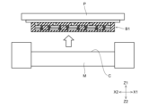
- FIG. 1 is a perspective view conceptually showing the shape of a coil component according to a first embodiment of the present invention.
- 2A to 2C are diagrams illustrating a structure of a coil conductive portion included in the coil component according to the first embodiment of the present invention.
- 3 is an XY plan view illustrating the structure of a first spiral conductive portion included in the coil component according to the first embodiment of the present invention.
- FIG. 4 is an XY plan view illustrating a structure of a second spiral conductive portion included in the coil component according to the first embodiment of the present invention.
- FIG. 1 is a cross-sectional view taken along an XZ plane illustrating a structure of a coil component according to a first embodiment of the present invention.
- FIG. 13 is an XY plan view illustrating the structure of a first spiral conductive portion included in a coil component according to a fifth embodiment of the present invention.
- FIG. 13 is a cross-sectional view taken along the XZ plane illustrating the structure of a coil component according to a fifth embodiment of the present invention.
- FIG. 13 is a cross-sectional view taken along the YZ plane illustrating the structure of a coil component according to a fifth embodiment of the present invention.
- FIG. 13 is an XY plan view illustrating the structure of a first spiral conductive portion included in a coil component according to a sixth embodiment of the present invention.
- FIG. 13 is a cross-sectional view taken along the XZ plane illustrating the structure of a coil component according to a sixth embodiment of the present invention.
- FIG. 13 is a cross-sectional view taken along the YZ plane illustrating the structure of a coil component according to a sixth embodiment of the present invention.
- FIG. 13 is an XY plan view illustrating the structure of a first spiral conductive portion included in a coil component according to a seventh embodiment of the present invention.
- FIG. 13 is a cross-sectional view taken along the XZ plane illustrating the structure of a coil component according to a seventh embodiment of the present invention.
- FIG. 13 is a cross-sectional view taken along the YZ plane illustrating the structure of a coil component according to a seventh embodiment of the present invention.
- FIG. FIG. 4 is a partial cross-sectional view showing an example of a second recess.
- 5A to 5C are explanatory diagrams illustrating an example of a manufacturing method for the coil component according to the first embodiment.
- 5A to 5C are explanatory diagrams illustrating an example of a manufacturing method for the coil component according to the first embodiment.
- 5A to 5C are explanatory diagrams illustrating an example of a manufacturing method for the coil component according to the first embodiment.
- 5A to 5C are explanatory diagrams illustrating an example of a manufacturing method for the coil component according to the first embodiment.
- 5A to 5C are explanatory diagrams illustrating an example of a manufacturing method for the coil component according to the first embodiment.
- 5A to 5C are explanatory diagrams illustrating an example of a manufacturing method for the coil component according to the first embodiment.
- 5A to 5C are explanatory diagrams illustrating an example of a manufacturing method for the coil component according to the first embodiment.
- 5A to 5C are explanatory diagrams illustrating an example of a manufacturing method for the coil component according to the first embodiment.
- 5A to 5C are explanatory diagrams illustrating an example of a manufacturing method for the coil component according to the first embodiment.
- 5A to 5C are explanatory diagrams illustrating an example of a manufacturing method for the coil component according to the first embodiment.
- 5A to 5C are explanatory diagrams illustrating an example of a manufacturing method for the coil component according to the first embodiment.
- 5A to 5C are explanatory diagrams illustrating an example of a manufacturing method for the coil component according to the first embodiment.
- 5A to 5C are explanatory diagrams illustrating an example of a manufacturing method for the coil component according to the first embodiment.
- 5A to 5C are explanatory diagrams illustrating an example of a manufacturing method for the coil component according to the first embodiment.
- 10A to 10C are explanatory diagrams illustrating an example of a manufacturing method for a coil component according to the second embodiment.
- 10A to 10C are explanatory diagrams illustrating an example of a manufacturing method for a coil component according to the second embodiment.
- 10A to 10C are explanatory diagrams illustrating an example of a manufacturing method for a coil component according to the second embodiment.
- 10A to 10C are explanatory diagrams illustrating an example of a manufacturing method for a coil component according to the second embodiment.
- 10A to 10C are explanatory diagrams illustrating an example of a manufacturing method for a coil component according to the second embodiment.
- 10A to 10C are explanatory diagrams illustrating an example of a manufacturing method for a coil component according to the second embodiment.
- 10A to 10C are explanatory diagrams illustrating an example of a manufacturing method for a coil component according to the second embodiment.
- 10A to 10C are explanatory diagrams illustrating an example of a manufacturing method for a coil component according to the second embodiment.
- 10A to 10C are explanatory diagrams illustrating an example of a manufacturing method for a coil component according to the second embodiment.
- 10A to 10C are explanatory diagrams illustrating an example of a manufacturing method for a coil component according to the second embodiment.
- 13A to 13C are explanatory diagrams illustrating an example of a manufacturing method for a coil component according to the third embodiment.
- 13A to 13C are explanatory diagrams illustrating an example of a manufacturing method for a coil component according to the third embodiment.
- 13A to 13C are explanatory diagrams illustrating an example of a manufacturing method for a coil component according to a fourth embodiment.
- 13A to 13C are explanatory diagrams illustrating an example of a manufacturing method for a coil component according to a fourth embodiment.
- 13A to 13C are explanatory diagrams illustrating an example of a manufacturing method for a coil component according to a fourth embodiment.
- 13A to 13C are explanatory diagrams illustrating an example of a manufacturing method for a coil component according to a fourth embodiment.
- 13A to 13C are explanatory diagrams illustrating an example of a manufacturing method for a coil component according to a fifth embodiment.
- 13A to 13C are explanatory diagrams illustrating an example of a manufacturing method for a coil component according to a fifth embodiment.
- 13A to 13C are explanatory diagrams illustrating an example of a manufacturing method for a coil component according to a fifth embodiment.
- 13A to 13C are explanatory diagrams illustrating an example of a manufacturing method for a coil component according to a fifth embodiment.
- 13A to 13C are explanatory diagrams illustrating an example of a manufacturing method for a coil component according to a fifth embodiment.
- 13A to 13C are explanatory diagrams illustrating an example of a manufacturing method for a coil component according to the sixth embodiment.
- 13A to 13C are explanatory diagrams illustrating an example of a manufacturing method for a coil component according to the sixth embodiment.
- 13A to 13C are explanatory diagrams illustrating an example of a manufacturing method for a coil component according to the sixth embodiment.
- 13A to 13C are explanatory diagrams illustrating an example of a manufacturing method for a coil component according to the sixth embodiment.
- 13A to 13C are explanatory diagrams illustrating an example of a manufacturing method for a coil component according to the sixth embodiment.
- 13A to 13C are explanatory diagrams illustrating an example of a manufacturing method for a coil component according to the sixth embodiment.
- 13A to 13C are explanatory diagrams illustrating an example of a manufacturing method for a coil component according to the sixth embodiment.
- 13A to 13C are explanatory diagrams illustrating an example of a manufacturing method for a coil component according to the sixth embodiment.
- 13A to 13C are explanatory diagrams illustrating an example of a manufacturing method for a coil component according to the sixth embodiment.
- 13A to 13C are explanatory diagrams illustrating an example of a manufacturing method for a coil component according to the sixth embodiment.
- 13A to 13C are explanatory diagrams illustrating an example of a manufacturing method for a coil component according to the sixth embodiment.
- 13A to 13C are explanatory diagrams illustrating an example of a manufacturing method for a coil component according to the sixth embodiment.
- 13A to 13C are explanatory diagrams illustrating an example of a manufacturing method for a coil component according to the sixth embodiment.
- 13A to 13C are explanatory diagrams illustrating an example of a manufacturing method for a coil component according to the sixth embodiment.
- 13A to 13C are explanatory diagrams illustrating an example of a manufacturing method for a coil component according to the sixth embodiment.
- 13A to 13C are explanatory diagrams illustrating an example of a manufacturing method for a coil component according to the sixth embodiment.
- 13A to 13C are explanatory diagrams illustrating an example of a manufacturing method for a coil component according to the sixth embodiment.
- 13A to 13C are explanatory diagrams illustrating an example of a manufacturing method for a coil component according to the sixth embodiment.
- 13A to 13C are explanatory diagrams illustrating an example of a manufacturing method for a coil component according to the sixth embodiment.
- 13A to 13C are explanatory diagrams illustrating an example of a manufacturing method for a coil component according to the sixth embodiment.
- 10A to 10C are explanatory diagrams illustrating an example of another manufacturing method for the coil component according to the second embodiment.
- 10A to 10C are explanatory diagrams illustrating an example of another manufacturing method for the coil component according to the second embodiment.
- 10A to 10C are explanatory diagrams illustrating an example of another manufacturing method for the coil component according to the second embodiment.
- 10A to 10C are explanatory diagrams illustrating an example of another manufacturing method for the coil component according to the second embodiment.
- 10A to 10C are explanatory diagrams illustrating an example of another manufacturing method for the coil component according to the second embodiment.
- 10A to 10C are explanatory diagrams illustrating an example of another manufacturing method for the coil component according to the second embodiment.
- 10A to 10C are explanatory diagrams illustrating an example of another manufacturing method for the coil component according to the second embodiment.
- 10A to 10C are explanatory diagrams illustrating an example of another manufacturing method for the coil component according to the second embodiment.
- 10A to 10C are explanatory diagrams illustrating an example of another manufacturing method for the coil component according to the second embodiment.
- 10A to 10C are explanatory diagrams illustrating an example of another manufacturing method for the coil component according to the second embodiment.
- 10A to 10C are explanatory diagrams illustrating an example of another manufacturing method for the coil component according to the second embodiment.
- 10A to 10C are explanatory diagrams illustrating an example of another manufacturing method for the coil component according to the second embodiment.
- 10A to 10C are explanatory diagrams illustrating an example of another manufacturing method for the coil component according to the second embodiment.
- 10A to 10C are explanatory diagrams illustrating an example of another manufacturing method for the coil component according to the second embodiment.
- 10A to 10C are explanatory diagrams illustrating an example of another manufacturing method for the coil component according to the second embodiment.
- 10A to 10C are explanatory diagrams illustrating an example of another manufacturing method for the coil component according to the second embodiment.
- 10A to 10C are explanatory diagrams illustrating an example of another manufacturing method for the coil component according to the second embodiment.
- 10A to 10C are explanatory diagrams illustrating an example of another manufacturing method for the coil component according to the second embodiment.
- 10A to 10C are explanatory diagrams illustrating an example of another manufacturing method for the coil component according to the second embodiment.
- 10A to 10C are explanatory diagrams illustrating an example of another manufacturing method for the coil component according to the second embodiment.
- 10A to 10C are explanatory diagrams illustrating an example of another manufacturing method for the coil component according to the second embodiment.
- 10A to 10C are explanatory diagrams illustrating an example of another manufacturing method for the coil component according to the second embodiment.
- 10A to 10C are explanatory diagrams illustrating an example of another manufacturing method for the coil component according to the second embodiment.
- 13A to 13C are explanatory diagrams illustrating an example of a manufacturing method for a coil component according to the seventh embodiment.
- 13A to 13C are explanatory diagrams illustrating an example of a manufacturing method for a coil component according to the seventh embodiment.
- 13A to 13C are explanatory diagrams illustrating an example of a manufacturing method for a coil component according to the seventh embodiment.
- 13A to 13C are explanatory diagrams illustrating an example of a manufacturing method for a coil component according to the seventh embodiment.
- 13A to 13C are explanatory diagrams illustrating an example of a manufacturing method for a coil component according to the seventh embodiment.
- 13A to 13C are explanatory diagrams illustrating an example of a manufacturing method for a coil component according to the seventh embodiment.
- 13A to 13C are explanatory diagrams illustrating an example of a manufacturing method for a coil component according to the seventh embodiment.
- 13A to 13C are explanatory diagrams illustrating an example of a manufacturing method for a coil component according to the seventh embodiment.
- 13A to 13C are explanatory diagrams illustrating an example of a manufacturing method for a coil component according to the seventh embodiment.
- 13A to 13C are explanatory diagrams illustrating an example of a manufacturing method for a coil component according to the seventh embodiment.
- 13A to 13C are explanatory diagrams illustrating an example of a manufacturing method for a coil component according to the seventh embodiment.
- 13A to 13C are explanatory diagrams illustrating an example of a manufacturing method for a coil component according to the seventh embodiment.
- 13A to 13C are explanatory diagrams illustrating an example of a manufacturing method for a coil component according to the seventh embodiment.
- 13A to 13C are explanatory diagrams illustrating an example of a manufacturing method for a coil component according to the seventh embodiment.
- 13A to 13C are explanatory diagrams illustrating an example of a manufacturing method for a coil component according to the seventh embodiment.
- 13A to 13C are explanatory diagrams illustrating an example of a manufacturing method for a coil component according to the seventh embodiment.
- 5A and 5B are explanatory diagrams illustrating an example of a land structure according to the embodiment.
- 5A and 5B are explanatory diagrams illustrating an example of a land structure according to the embodiment.
- FIG. 5A to 5C are schematic cross-sectional views illustrating a mounting state of a support member.
- 5A to 5C are schematic cross-sectional views illustrating a mounting state of a support member.
- 11 is an explanatory diagram of another example of the structure of the land according to the embodiment.
- FIG. 5A to 5C are schematic cross-sectional views illustrating a mounting state of a support member.
- FIG. 1 is a perspective view conceptually illustrating the shape of a coil component according to the first embodiment of the present invention.
- FIG. 2 is a view illustrating the structure of a coil conductive portion included in the coil component according to the first embodiment of the present invention.
- the coil conductive portion is drawn with a solid line
- the main body portion is drawn with a dashed line
- other components are omitted.
- FIG. 3 is an XY plan view illustrating the structure of a first spiral conductive portion included in the coil component according to the first embodiment of the present invention.
- FIG. 4 is an XY plan view illustrating the structure of a second spiral conductive portion included in the coil component according to the first embodiment of the present invention.
- FIGS. 5A and 5B are cross-sectional views illustrating the structure of a coil portion included in the coil component according to the first embodiment of the present invention. Note that FIG. 2 is a view from the Z1 side in the Z1-Z2 direction, and FIG.
- FIG. 3 is a view from the Z1 side in the Z1-Z2 direction, and only the coil conductive portion in the coil portion is shown, and the main body portion, terminal portion, and exterior coat are shown with dashed lines.
- Fig. 4 only the coil conductive portion as viewed from the Z2 side in the Z1-Z2 direction is depicted.
- Fig. 5A the main body, terminals, and exterior coating are shown with dashed lines, and the cross section taken along line A-A' in Fig. 3 is shown as an XZ cross section.
- Fig. 5B the main body and exterior coating are shown with dashed lines, and the cross section taken along line B-B' in Fig. 3 is shown as a YZ cross section.
- the coil component 100A includes a coil portion 10 having a coil conductive portion 20, a main body portion 30, a first terminal portion 41, a second terminal portion 42, exterior coatings 50 and 60, and support portions 701A and 701B.
- the first spiral conductive unit 11 has a conductor arranged in a spiral shape that moves away from the axis O in a clockwise direction from one end 12 to the other end 13, as viewed from the Z1 side in the Z1-Z2 direction.
- the "spiral direction" of the spiral conductive unit means the direction from the end on the inner circumference side to the end on the outer circumference side.
- the conductor (conductive material) constituting the coil conductive part 20 is not limited as long as it has appropriate conductivity. Specific examples of the conductor constituting the coil conductive part 20 include copper, copper alloys, aluminum, and aluminum alloys, and the coil conductive part 20 can be manufactured using a film forming technique such as plating.
- the coil part 10 has an insulating coil insulation part (not shown in Figures 1 to 4) on the surface of the coil conductive part 20. This coil insulation part ensures insulation between adjacent conductors in the coil conductive part 20 (between the surfaces of the conductors facing each other).
- the coil insulation part is made of, for example, a resin material. No coil insulation part is provided at the ends of the two ends (first lead part 14, second lead part 24) of the coil conductive part 20, and the coil part 10 can be electrically connected to other members at these ends.
- the coil conductive portion 20 includes a second conductive portion 202 having a second spiral conductive portion 21 arranged alongside the first spiral conductive portion 11 in the first direction. That is, in this embodiment, the coil conductive portion 20 includes a plurality of spiral portions, specifically, the coil conductive portion 20 includes two spiral portions consisting of the first spiral conductive portion 11 and the second spiral conductive portion 21.
- the second spiral conductive portion 21 has a spiral shape that moves away from the axis O along the first direction (Z1-Z2 direction) from one end 22, which is the inner end of the second spiral conductive portion 21, towards the other end 23, which is the outer end of the second spiral conductive portion 21.
- the conductor when viewed from the Z1 side in the Z1-Z2 direction, the conductor is arranged in a spiral shape that moves away from the axis O in the opposite direction to the first spiral conductive portion 11 (counterclockwise in FIG. 2).
- the average value of the separation distance in the first direction (Z1-Z2 direction) between the first spiral conductive portion 11 and the second spiral conductive portion 21 is not particularly limited. The smaller this separation distance is, the easier it is to reduce the height (dimension in the Z1-Z2 direction) of the coil component 100, but if it is too small, the insulation between the first spiral conductive portion 11 and the second spiral conductive portion 21 is likely to decrease.
- the separation distance is 0.4 ⁇ m or more and 20 ⁇ m or less. In terms of manufacturing, this distance is preferably 1.0 ⁇ m or more, and even more preferably 5.0 ⁇ m or more, in order to reduce variation in the distance and to more reliably support the coil in the same plane.
- One end 12 of the first spiral conductive portion 11 and one end 22 of the second spiral conductive portion 21 are electrically connected by a via portion VP.
- the via portion VP may be made of the same conductor as the coil conductive portion 20.
- the via portion VP is made of the same material as the first spiral conductive portion 11 and the second spiral conductive portion 21, and is manufactured simultaneously with the first spiral conductive portion 11 and the second spiral conductive portion 21.
- the via portion VP is integrated with one end 12 of the first spiral conductive portion 11 and one end 22 of the second spiral conductive portion 21.
- the first lead-out portion 14 is connected to the other end 13 of the first spiral conductive portion 11 as a part of the first conductive portion 201, and the second lead-out portion 24 is connected to the other end 23 of the second spiral conductive portion 21 as a part of the second conductive portion 202. Therefore, the other end 13 of the first spiral conductive portion 11 is essentially an interface with the first lead-out portion 14, and the other end 23 of the second spiral conductive portion 21 is essentially an interface with the second lead-out portion 24.
- the first lead-out portion 14 and the second lead-out portion 24 are made of the same material as the first spiral conductive portion 11 and the second spiral conductive portion 21, and are manufactured simultaneously with the first spiral conductive portion 11 and the second spiral conductive portion 21.
- the first conductive portion 201 is manufactured as a single unit, and the second conductive portion 202 is also manufactured as a single unit.
- the first lead-out portion 14 is seamlessly integrated with the other end 13 of the first spiral conductive portion 11, and the second lead-out portion 24 is seamlessly integrated with the other end 23 of the second spiral conductive portion 21.
- the coil conductive portion 20 has a first conductive portion 201 having a first spiral conductive portion 11 and a first pull-out portion 14, a second conductive portion 202 having a second spiral conductive portion 21 and a second pull-out portion 24, and a via portion VP, which are formed from a common conductive material.
- the main body 30 includes magnetic powder and has an outer surface having a plurality of surfaces extending in a first direction and two intersecting surfaces aligned in the first direction.
- the main body 30 covers at least a part of the coil section 10 with the two intersecting surfaces.
- the main body 30 has a substantially rectangular parallelepiped shape and has, as a plurality of surfaces, two outer surfaces 30a, 30b aligned in the X1-X2 direction and two outer surfaces 30c, 30d aligned in the Y1-Y2 direction, and has two intersecting surfaces 30e, 30f aligned in the first direction.
- the main body 30 also includes a portion other than the outermost end surface (X2 side in the X1-X2 direction) of the first lead section 14 and the outermost end surface (X1 side in the X1-X2 direction) of the second lead section 24, which are located at the end of the coil section 10.
- the structure of the magnetic powder is not limited. This structure may include a crystalline phase or an amorphous phase.
- a crystalline material is defined as a material consisting of a crystalline phase, an amorphous material as a material consisting of an amorphous phase, and a composite material as a material consisting of a crystalline phase and an amorphous material. If the diffraction spectrum obtained by a general X-ray diffraction method includes a sharp diffraction peak that can identify the type of crystalline phase, the material includes a crystalline phase. If the diffraction spectrum obtained by a general X-ray diffraction method includes a broad peak indicating an amorphous phase, the material includes an amorphous phase. If the DSC curve obtained by differential thermal analysis includes a peak indicating crystallization, i.e., heat generation associated with a phase change from an amorphous phase to a crystalline phase, the material includes an amorphous phase.
- the material system of the magnetic powder is not limited.
- crystalline materials include Fe-Si-Cr alloys, Fe-Ni alloys, Fe-Co alloys, Fe-V alloys, Fe-Al alloys, Fe-Si alloys, Fe-Si-Al alloys, pure iron, and ferrite.
- Carbonyl iron powder is preferable as pure iron powder.
- amorphous materials include Fe-Si-B alloys, Fe-P-C alloys, and Co-Fe-Si-B alloys.
- composite materials include Fe-Zr alloys, Fe-Zr-B alloys, Fe-Si-B-Nb-Cu alloys, and Fe-Si-B-P-Cu alloys. If the magnetic powder is a metal powder containing Fe, the synergistic effect of improving the magnetic properties is particularly large.
- an Fe-Si-Cr alloy may be composed of 1.0-10.0 mass% Si, 1.0-10.0 mass% Cr, and the remainder composed of Fe and impurities.
- an Fe-Ni alloy may be composed of 1.0-99.0 mass% Ni, and the remainder composed of Fe and impurities.
- an Fe-P-C alloy may be composed of 1.0-13.0 atomic% P, 1.0-13.0 atomic% C, Fe, and impurities. This Fe-P-C alloy may contain one or more optional elements selected from the group consisting of Ni, Sn, Cr, B, and Si.
- the amount of Ni may be 0 to 10.0 atomic %
- the amount of Sn may be 0 to 3.0 atomic %
- the amount of Cr may be 0 to 6.0 atomic %
- the amount of B may be 0 to 9.0 atomic %
- the amount of Si may be 0 to 7.0 atomic %.
- the amount of Fe is preferably 65 atomic % or more.
- the Fe-Si-B-Nb-Cu alloy may be composed of 1.0 to 16.0 atomic % Si, 1.0 to 15.0 atomic % B, 0.50 to 5.0 atomic % Nb, 0.50 to 5.0 atomic % Cu, and the balance consisting of Fe and impurities.
- the amount of Fe is preferably 65 atomic % or more.
- the shape of the magnetic powder is not limited.
- the magnetic powder may be spherical, elliptical, scaly, or of an irregular shape.
- the manufacturing method for obtaining these shapes is also not limited.
- the particle size distribution of the magnetic powder is not limited.
- the particle size distribution of the magnetic powder can be obtained, for example, by analyzing an image (secondary electron image) obtained by capturing an image of a cut surface of the main body 30 with a scanning electron microscope.
- the average equivalent circle diameter of the magnetic powder may be 0.50 to 50.0 ⁇ m.
- the distribution of the equivalent circle diameter may include multiple peaks.
- the magnetic powder may be subjected to a surface insulating treatment.
- a surface insulating treatment When the magnetic powder is subjected to a surface insulating treatment, the insulation resistance of the main body 30 is improved.
- the magnetic powder may have an insulating coating on the surface of the magnetic particles. This insulating coating may contain at least one element selected from the group consisting of Si, P, and B, and O (oxygen).
- the magnetic powder may be a mixed material in which multiple powder materials are mixed.
- This magnetic powder is preferably a ferromagnetic material, and more preferably a soft magnetic material.
- the main body 30 may further include an optional auxiliary material.
- the optional auxiliary material is, for example, a binder material or a modifier.
- the binder material bonds particles such as magnetic powder contained in the main body 30 together.
- This binder material is preferably an insulating material to provide insulation resistance to the main body 30.
- the binding material may be an organic material or an inorganic material.
- the organic material may be a resin material.
- the resin material include acrylic resin, silicone resin, epoxy resin, phenol resin, urea resin, melamine resin, and polyester resin.
- the inorganic material may be a glass-based material such as water glass.
- the binding material may be a product of a reaction such as thermal decomposition, or a mixture of multiple materials.
- the modifier for example, improves the fluidity of the powder or adjusts the hardening speed of the binder material.
- the modifier may be a glass-based material.
- the dimensions of the main body 30 are not limited.
- the maximum dimension of the main body 30 may be 3.2 mm or less.
- Example terminal 2 the outermost end face (drawn-out portion exposed surface 140) of the first drawn-out portion 14 (on the X2 side in the X1-X2 direction) and the outermost end face (drawn-out portion exposed surface 240) of the second drawn-out portion 24 (on the X1 side in the X1-X2 direction), which are located at the end of the coil portion 10, are exposed from the main body portion 30 at side faces aligned in the X1-X2 direction of the main body portion 30.
- a first terminal portion 41 is provided so as to be in electrical contact with the drawn-out portion exposed surface 140
- a second terminal portion 42 is provided so as to be in electrical contact with the drawn-out portion exposed surface 240.
- the first terminal portion 41 has a side portion 41a that covers the side surface of the main body portion 30 on the X2 side in the X1-X2 direction.
- the second terminal portion 42 has a side portion 42a that covers the side surface of the main body portion 30 on the X1 side in the X1-X2 direction.
- the first terminal portion 41 may have a bottom surface portion that is provided so as to cover part of the bottom surface (the surface on the Z2 side in the Z1-Z2 direction) of the main body portion 30.
- the second terminal portion 42 may have a bottom surface portion that is provided on the bottom surface of the main body portion 30 so as to cover part of the bottom surface while being spaced apart from the bottom surface portion of the first terminal portion 41.
- the positions of the first terminal portion 41 and the second terminal portion 42 are not limited to the above positions.
- the first terminal portion 41 and the second terminal portion 42 may be formed to cover a part of the upper surface (the surface on the Z1 side in the Z1-Z2 direction) of the main body portion 30.
- the first terminal portion 41 and the second terminal portion 42 may be provided only on a part of the bottom surface (the surface on the Z2 side in the Z1-Z2 direction) of the main body portion 30.
- the coil conductive portion 20 may have a connection conductive portion (not shown) that connects the two ends of the coil portion 10 (the first pull-out portion 14, the second pull-out portion 24) to the bottom surface of the main body portion 30 through the inside of the main body portion 30.
- the two ends of the coil portion 10 (the pull-out portion exposed surfaces 140, 240) may not be exposed to the side surfaces of the main body portion 30, and the connection conductive portion may be exposed to the bottom surface of the main body portion 30.
- the material and configuration of the first terminal portion 41 and the second terminal portion 42 are not limited as long as they have appropriate conductivity.
- One non-limiting example of the first terminal portion 41 and the second terminal portion 42 is a layer having a structure of Cu plating/Ni plating/Sn plating from the side proximal to the surface of the main body portion 30.
- the first terminal portion 41 and the second terminal portion 42 may be composed of a coated electrode in which a conductive material such as silver is dispersed in a resin or the like.
- the first terminal portion 41 and the second terminal portion 42 may also be a combination of plating and a coated electrode.
- An insulating exterior coat 50, 60 is provided as an insulating layer on one intersecting surface 30f located on the Z2 side of the main body 30 in the Z1-Z2 direction Z2 and on the side surfaces aligned in the Y1-Y2 direction.
- the exterior coat 50, 60 may be provided on the mounting surface of the coil component 100A (the surface on the side of one intersecting surface 30e located on the Z1 side of the main body 30 in the Z1-Z2 direction Z1).
- an insulating exterior coat may be provided on a part of the one intersecting surface 30e of the main body 30 where these bottom surface portions are not provided.
- the exterior coat 50, 60 may include a layer made of a resin having an average thickness of 0.10 ⁇ m to 10.0 ⁇ m. This makes it easy to maintain the magnetic properties of the coil part 100A, to increase the reliability of the coil part 100A by improving the insulation of the surface of the coil part 100A, and to improve the appearance of the coil part 100A.
- the coil part 100A does not need to have the exterior coats 50, 60.
- the exterior coats 50, 60 can be formed at any position on the surface of the main body 30 depending on the purpose.
- the coil component 100A includes a non-spiral shaped first dummy conductive portion 72 and a second dummy conductive portion 71.
- the first dummy conductive portion 72 faces the first lead-out portion 14 in the first direction (Z1-Z2 direction) with the first insulating portion 90 interposed therebetween, and has a portion in contact with the first insulating portion 90.
- the first dummy conductive portion 72 is also spaced apart from the second conductive portion 202 (specifically, the second outer periphery turn 213) in a direction intersecting the first direction (specifically, the X1-X2 direction).
- the first dummy conductive portion 72 and the first pull-out portion 14 are electrically insulated. Therefore, the first dummy conductive portion 72 is electrically insulated from both the first conductive portion 201 and the second conductive portion 202.
- the outer end (the X2 side in the X1-X2 direction) of the first dummy conductive portion 72 (dummy end surface portion 72E) is exposed, but this is not limited thereto.
- the second insulating portion 80 may be provided so as to come into contact with the dummy end surface portion 72E.
- the configuration of the second dummy conductive portion 71 is the same as that of the first dummy conductive portion 72. That is, the second dummy conductive portion 71 faces the second pull-out portion 24 in the first direction (Z1-Z2 direction) across the first insulating portion 90, has a portion in contact with the first insulating portion 90, and is spaced apart from the first conductive portion 201 (specifically, the first outer circumferential turn 113) in a direction intersecting the first direction (specifically, the X1-X2 direction). By being arranged in this manner, the second dummy conductive portion 71 is also electrically insulated from both the first conductive portion 201 and the second conductive portion 202.
- first dummy conductive portion 72 and the first conductive portion 201 are electrically connected to each other by the first terminal portion 41, and therefore do not necessarily need to be insulated.
- the second dummy conductive portion 71 and the second conductive portion 202 are electrically connected to each other by the second terminal portion 42, and therefore do not necessarily need to be insulated. Therefore, the first dummy conductive portion 72 and the first conductive portion 201 may be in direct contact with each other, or may be electrically connected through a conductor portion in a via.
- the second dummy conductive portion 71 and the second conductive portion 202 may be in direct contact with each other, or may be electrically connected through a conductor portion in a via. Such an electrical connection is effective in widening the current path of the coil portion and reducing the DCR.
- the coil insulating portion includes a first insulating portion 90 that contacts one of the ends of the first spiral conductive portion 11 on the first direction side, specifically, at least a part of the end of the side (Z2 side in the Z1-Z2 direction) facing the second spiral conductive portion 21.
- the first insulating portion 90 is interposed between the first spiral conductive portion 11 and the second spiral conductive portion 21 arranged in the first direction, and contacts both of them. In this manner, the first insulating portion 90 contacts the first spiral conductive portion 11, thereby reliably insulating the first spiral conductive portion 11. Furthermore, as shown in the cross-sectional view of Fig. 5B, the first insulating portion 90 contacts both the first spiral conductive portion 11 and the second spiral conductive portion 21, thereby reliably preventing a short circuit between the first spiral conductive portion 11 and the second spiral conductive portion 21.
- the material constituting the first insulating part 90 is not limited as long as it has an appropriate insulating property.
- the first insulating part 90 may preferably have a volume resistivity of 1.0 ⁇ 10 14 ⁇ cm or more obtained by ASTM D257. This volume resistivity is more preferably 1.0 ⁇ 10 15 ⁇ cm or more, and even more preferably 1.0 ⁇ 10 16 ⁇ cm or more.
- the upper limit of the volume resistivity is not particularly limited.
- the volume resistivity may be 1.0 ⁇ 10 20 ⁇ cm or less.
- the first insulating part 90 has excellent dielectric properties, and specifically, it may be preferable that the relative dielectric constant at 60 Hz obtained by ASTM D150 is 4.0 or less.
- This relative dielectric constant is more preferably 3.5 or less, and even more preferably 3.0 or less.
- the lower limit of this relative dielectric constant is not particularly limited.
- the relative dielectric constant may be 1.0 or more.
- the method for measuring the volume resistivity and relative dielectric constant of the first insulating part 90 is not limited. For example, a measurement sample is separately prepared by adjusting a material corresponding to the first insulating portion 90 to the dimensions required for measurement, and the constituent materials are identified using analytical techniques such as component analysis and FT-IR using this measurement sample, and the characteristics of the material, such as volume resistivity, are evaluated.
- the material constituting the first insulating section 90 may be made of an organic material, may be made of an inorganic material, or may be a composite material of an organic material and an inorganic material.
- the inorganic material may have a particulate shape and may be dispersed in a matrix made of an organic material.
- organic materials include polyimide resin, polyethylene resin, polypropylene resin, polyamide resin, polyester resin, polyamideimide resin, polysulfone resin, polycarbonate resin, liquid crystal polymer resin, polyvinylidene fluoride resin, and polytetrafluoroethylene resin.
- the coil insulating portion has a second insulating portion 80, and as shown in FIG. 5A, the second insulating portion 80 is provided on at least a portion of the surface of the first spiral conductive portion 11 and the surface of the second spiral conductive portion 21.
- the material constituting the second insulating section 80 is not limited as long as it has appropriate insulating properties.
- the second insulating section 80 is thermoplastic and includes a thermoplastic resin including a paraxylylene-based polymer.
- thermoplastic resins include polyethylene, polypropylene, polyamide, polyester, polyamideimide, polyimide, polysulfone, polycarbonate, liquid crystal polymer, polyvinylidene fluoride, and polytetrafluoroethylene.
- the second insulating section 80 is preferably thermoplastic as a whole, and may contain, in addition to the above-mentioned thermoplastic resin, for example, inorganic insulating particles.
- the second insulating section 80 may also be made of the same material as the first insulating section 90.
- the second insulating part 80 is preferably excellent in insulation properties, and specifically, in some cases, the volume resistivity obtained by ASTM D257 is preferably 1.0 ⁇ 10 14 ⁇ cm or more. This volume resistivity is more preferably 1.0 ⁇ 10 15 ⁇ cm or more, and even more preferably 1.0 ⁇ 10 16 ⁇ cm or more. The upper limit of the volume resistivity is not particularly limited. The volume resistivity may be 1.0 ⁇ 10 20 ⁇ cm or less.
- the second insulating part 80 is preferably excellent in dielectric properties, and specifically, in some cases, the relative dielectric constant at 60 Hz obtained by ASTM D150 is preferably 4.0 or less. This relative dielectric constant is more preferably 3.5 or less, and even more preferably 3.0 or less.
- the lower limit of this relative dielectric constant is not particularly limited.
- the relative dielectric constant may be 1.0 or more.
- a material corresponding to the second insulating part 80 prepared separately is adjusted to the dimensions required for the measurement and used.
- the material corresponding to the second insulating section 80 can be identified, as in the case of the first insulating section 90, by an analysis method such as component analysis or FT-IR.
- the support parts 701A and 701B are, for example, solder balls, hetero-nuclear solder balls (copper-nuclear solder balls, resin-core solder balls, etc.), or pillar members made of conductive material (copper, etc.).
- the support parts 701A and 701B contact the coil part 10 to form a first interface 70A that intersects with the first direction (Z1-Z2 direction).
- the support parts 701A and 701B are arranged on the Z1 side of the coil part 10 in the Z1-Z2 direction.
- the support part 701A is arranged on the Z1 side of the first drawn part 14 in the Z1-Z2 direction
- the support part 701B is arranged on the Z1 side of the first dummy conductive part 72 in the Z1-Z2 direction. That is, the support parts 701A and 701B are provided in the center part in the Y1-Y2 direction at the end parts of the main body part 30 in the X1-X2 direction.
- the support portion 701A overlaps with the first pull-out portion 14 and the first dummy conductive portion 72 of the coil portion 10
- the support portion 701B overlaps with the second pull-out portion 24 and the first dummy conductive portion 72 of the coil portion 10.
- the first interface 70A may be a contact interface between the conductive surface of the support conductor part and the conductive surface of the coil conductive part 20.
- the support parts 701A, 701B have a conductive support conductor part
- at least a part of the first exposed surface 70C of the support exposed surface 70B may be an exposed conductive surface made of the support conductor part.
- a first terminal portion 41 is provided on the outer surface 30a, and a second terminal portion 42 is provided on the outer surface 30b.
- the joining strength and conductivity between the coil conductive portion 20 and the first terminal portion 41 and the second terminal portion 42 are increased, and the connection area with the conductive material (external terminal or solder) of the coil component 100A can be increased.
- the first dummy conductive portion 72 has a dummy end surface portion 72E exposed from the outer surface of the main body portion 30.
- the first lead portion 14 and the second lead portion 24 have end surfaces (lead portion exposed surfaces 140, 240) exposed from the outer surface of the main body portion 30.
- the first terminal portion 41 is joined to the dummy end surface portion 72E and the lead portion exposed surface 140, and the second terminal portion 42 is joined to the dummy end surface portion 71E and the lead portion exposed surface 240.
- the bonding strength and conductivity between the coil conductive portion 20 and the first terminal portion 41 and the second terminal portion 42 are increased, and the connection area with the conductive material (external terminal or solder) of the coil component 100A can be increased.
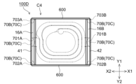
- Fig. 6 is an XY plan view for explaining the structure of a first spiral conductive part included in a coil component according to a second embodiment of the present invention.
- the coil conductive part is drawn with a solid line
- the main body part is drawn with a dashed line
- other components are omitted.
- Figs. 7A and 7B are cross-sectional views for explaining the structure of a coil part included in a coil component according to a second embodiment of the present invention. Note that Fig. 7A shows a cross section taken along line AA' in Fig. 6 as an XZ cross section, and Fig. 7B shows a cross section taken along line BB' in Fig. 6 as a YZ cross section.
- first connecting portions 15A, 15B, 15C, and 15D are provided on two outer side surfaces 30a and 30b of the main body portion 30 parallel to the YZ plane.
- the first connecting portion 15A is connected to the first lead portion 14 and is provided extending in the Y1-Y2 direction on the Z1-Z2 direction Z1 side of the first insulating portion 90.
- the first connecting portion 15A is provided so as to cross two outer side surfaces 30c and 30d of the main body portion 30 parallel to the XZ plane.
- the first connecting portion 15A is made of the same material as the first spiral conductive portion 11 and the first lead portion 14, and is manufactured simultaneously with the first spiral conductive portion 11 and the first lead portion 14.
- the first connecting portion 15A connected to the first pull-out portion 14 is included in the coil conductive portion 20.
- the first connecting portion 15A can also be part of the first pull-out portion 14. In this case, the surface of the first connecting portion 15A exposed from the main body portion 30 becomes the pull-out portion exposed surface 140.
- the first connecting portion 15B is connected to the second dummy conductive portion 71 and is provided on the Z1-Z2 direction Z1 side of the first insulating portion 90, extending in the Y1-Y2 direction.
- the first connecting portion 15B is provided across two outer surfaces 30c, 30d parallel to the XZ plane of the main body portion 30.
- the first connecting portion 15B is made of the same material as the first spiral conductive portion 11 and the first dummy conductive portion 72, and is manufactured simultaneously with the first spiral conductive portion 11 and the first dummy conductive portion 72.
- the first connecting portion 15B can also be a part of the first dummy conductive portion 72. In this case, the surface of the first connecting portion 15B exposed from the outer surface 30b of the main body portion 30 becomes the dummy end surface portion 71E.
- the first connecting portion 15C is connected to the first dummy conductive portion 72 and is provided on the Z1-Z2 direction Z2 side of the first insulating portion 90, extending in the Y1-Y2 direction.
- the first connecting portion 15C is provided across two outer surfaces 30c, 30d parallel to the XZ plane of the main body portion 30.
- the first connecting portion 15C is made of the same material as the second spiral conductive portion 21 and the first dummy conductive portion 72, and is manufactured simultaneously with the second spiral conductive portion 21 and the first dummy conductive portion 72.
- the first connecting portion 15C can also be a part of the first dummy conductive portion 72. In this case, the surface of the first connecting portion 15C exposed from the outer surface 30a of the main body portion 30 becomes the dummy end surface portion 72E.
- the first connecting portion 15D is connected to the second pull-out portion 24 and is provided extending in the Y1-Y2 direction on the Z1-Z2 direction Z2 side of the first insulating portion 90.
- the first connecting portion 15D is provided across two outer surfaces 30c, 30d parallel to the XZ plane of the main body portion 30.
- the first connecting portion 15D is made of the same material as the second spiral conductive portion 21 and the second pull-out portion 24 and is manufactured simultaneously with the second spiral conductive portion 21 and the second pull-out portion 24.
- the first connecting portion 15D connected to the second pull-out portion 24 is included in the coil conductive portion 20.
- the first connecting portion 15D When the first connecting portion 15D is provided integrally with the second pull-out portion 24, the first connecting portion 15D can also be part of the second pull-out portion 24. In this case, the surface of the first connecting portion 15D exposed from the main body portion 30 becomes the drawer exposed surface 240.
- the support parts 704A and 704B similar to the support parts 701A and 701B, for example, solder balls, heteronuclear solder balls (copper core solder balls, resin core solder balls, etc.), and pillar members made of conductive materials (copper, etc.) are used.
- the support parts 704A and 704B contact the coil part 10 to form a first interface 70A that intersects with the first direction (Z1-Z2 direction).
- the support parts 704A and 704B are arranged on the Z2 side of the coil part 10 in the Z1-Z2 direction.
- the support part 704A is arranged on the Z2 side of the first dummy conductive part 72 in the Z1-Z2 direction
- the support part 704B is arranged on the Z2 side of the second drawn part 24 in the Z1-Z2 direction. That is, the support parts 704A and 704B are provided in the center part in the Y1-Y2 direction at each end part in the X1-X2 direction of the main body part 30.
- the support portion 704A overlaps with the first pull-out portion 14 and the first dummy conductive portion 72 of the coil portion 10
- the support portion 704B overlaps with the second pull-out portion 24 and the first dummy conductive portion 72 of the coil portion 10.
- the support portions 704A and 704B have a support exposed surface 70B exposed from the main body portion 30, and this support exposed surface 70B includes a first exposed surface 70C having an in-plane direction along the first direction.
- the first exposed surface 70C is exposed from two outer surfaces 30a and 30b of the main body portion 30 that are parallel to the YZ plane.
- the first interface 70A may be a contact interface between the conductive surface of the support conductor part and the conductive surface of the coil conductive part 20.
- the support parts 704A, 704B have a conductive support conductor part
- at least a part of the first exposed surface 70C of the support exposed surface 70B may be an exposed conductive surface made of the support conductor part.
- a first terminal portion 41 is provided on the outer surface 30a, and a second terminal portion 42 is provided on the outer surface 30b.
- the joining strength and conductivity between the coil conductive portion 20 and the first terminal portion 41 and the second terminal portion 42 are increased, and the connection area with the conductive material (external terminal or solder) of the coil component 100B can be increased.
- support parts 702A, 702B, 703A, 703B, 705A, 705B, 706A, 706B similar to the support parts 701A, 701B, 704A, 704B, for example, solder balls, heteronuclear solder balls (copper core solder balls, resin core solder balls, etc.), and pillar members made of conductive materials (copper, etc.) are used.
- the support parts 702A, 702B, 703A, 703B, 705A, 705B, 706A, 706B contact the coil part 10 and form a first interface 70A that intersects with the first direction (Z1-Z2 direction).
- the support parts 702A, 702B, 703A, 703B are arranged on the Z1 side of the coil part 10 in the Z1-Z2 direction. Specifically, support parts 702A and 703A are disposed on the Z1 side of first connecting part 15A in the Z1-Z2 direction, and support parts 702B and 703B are disposed on the Z1 side of first connecting part 15B in the Z1-Z2 direction. Each of support parts 702A, 702B, 703A, and 703B is provided at a corner of main body part 30.
- support parts 705A, 705B, 706A, and 706B are arranged on the Z2 side of the coil part 10 in the Z1-Z2 direction. Specifically, support parts 705A and 706A are arranged on the Z2 side of the first connecting part 15C in the Z1-Z2 direction, and support parts 705B and 706B are arranged on the Z2 side of the first connecting part 15D in the Z1-Z2 direction. Each of support parts 705A, 705B, 706A, and 706B is provided at a corner of the main body part 30.
- Supporting parts 702A, 702B, 703A, 703B, 705A, 705B, 706A, 706B have a supporting exposed surface 70B exposed from the main body part 30, and this supporting exposed surface 70B includes a first exposed surface 70C having an in-plane direction along the first direction. That is, the first exposed surface 70C of supporting parts 702A, 705A arranged at the corner between outer surface 30a and outer surface 30c is exposed from outer surface 30a, 30c. The first exposed surface 70C of supporting parts 703A, 706A arranged at the corner between outer surface 30a and outer surface 30d is exposed from outer surface 30a, 30d.
- the first exposed surface 70C of supporting parts 702B, 705B arranged at the corner between outer surface 30b and outer surface 30c is exposed from outer surface 30b, 30c.
- the first exposed surfaces 70C of the support parts 703B and 706B, which are located at the corners between the outer surfaces 30b and 30d, are exposed from the outer surfaces 30b and 30d.
- the support exposed surface 70B may include a second exposed surface 70D that intersects with the first direction. At least a portion of the second exposed surface 70D is made of an exposed conductive surface. That is, the second exposed surfaces 70D of the support parts 703A, 703B, 704A, and 704B are exposed from the outer surface of the main body part 30 on the Z1 side in the Z1-Z2 direction, and the second exposed surfaces 70D of the support parts 705A, 705B, 706A, and 706B are exposed from the outer surface of the main body part 30 on the Z2 side in the Z1-Z2 direction. As a result, the exposed conductive surface becomes a part of the outermost surface of the coil part 100B.
- the exterior coats 50 and 60 may be appropriately extended toward the second exposed surface 70D and brought into contact with the second exposed surface 70D. Furthermore, to improve the peel strength of the first terminal portion 41 and the second terminal portion 42, the first terminal portion 41 and the second terminal portion 42 may be extended toward the second exposed surface 70D and brought into contact with the second exposed surface 70D.
- the support parts 702A, 702B, 703A, 703B, 705A, 705B, 706A, and 706B have conductive support conductor parts
- at least a part of the first interface 70A may be a contact interface between the conductive surface of the support conductor part and the conductive surface of the coil conductive part 20.
- at least a part of the first exposed surface 70C of the exposed support surface 70B may be an exposed conductive surface made of the support conductor part.
- a first terminal portion 41 is provided on the outer surface 30a, and a second terminal portion 42 is provided on the outer surface 30b.
- the first terminal portion 41 is joined to the lead-out portion exposed surface 140, the connecting portion exposed surface 150, and the first exposed surface 70C exposed from the outer surface 30a
- the second terminal portion 42 is joined to the lead-out portion exposed surface 240, the connecting portion exposed surface 150, and the first exposed surface 70C exposed from the outer surface 30b, thereby increasing the bonding strength and conductivity between the coil conductive portion 20 and the first terminal portion 41 and the second terminal portion 42, and increasing the connection area with the conductive material (external terminal or solder) of the coil component 100B.
- Fig. 8 is an XY plan view for explaining the structure of a first spiral conductive part included in a coil component according to a third embodiment of the present invention.
- the coil conductive part is drawn with a solid line
- the main body part is drawn with a dashed line
- other components are omitted.
- Figs. 9A and 9B are cross-sectional views for explaining the structure of a coil part included in a coil component according to a third embodiment of the present invention. Note that Fig. 9A shows a cross section taken along line AA' in Fig. 8 as an XZ cross section, and Fig. 9B shows a cross section taken along line BB' in Fig. 8 as a YZ cross section.
- the external electrodes 16A, 16B are provided extending in the Y1-Y2 direction on the Z1 side in the Z1-Z2 direction of the main body 30.
- the external electrode 16A contacts an exposed conductive surface on the supporting exposed surface 70B of the supporting portion 701A
- the external electrode 16B contacts an exposed conductive surface on the supporting exposed surface 70B of the supporting portion 701B.
- This exposed conductive surface is a part of the outermost surface of the main body 30.
- the external electrodes 16A, 16B are arranged across two outer surfaces 30c, 30d of the main body 30 that are parallel to the XZ plane.
- the external electrodes 16A, 16B may have a first recess 161 that is recessed in a first direction (the Z2 side in the Z1-Z2 direction). This reduces the volume (height) occupied by the coil component 100C after soldering due to the concave surface of the first recess 161.
- a first terminal portion 41 may be provided on the outer surface 30a, and a second terminal portion 42 may be provided on the outer surface 30b.
- the first terminal portion 41 is joined to the lead-out portion exposed surface 140, the dummy end surface portion 72E, the first exposed surface 70C, and the external electrode 16A exposed from the outer surface 30a
- the second terminal portion 42 is joined to the lead-out portion exposed surface 240, the dummy end surface portion 71E, the first exposed surface 70C, and the external electrode 16B exposed from the outer surface 30b.
- This increases the bonding strength and conductivity between the coil conductive portion 20 and the first terminal portion 41 and the second terminal portion 42, and increases the connection area with the conductive material (external terminal or solder) of the coil component 100C.
- Fig. 10 is an XY plan view for explaining the structure of a first spiral conductive part included in a coil component according to a fourth embodiment of the present invention.
- the coil conductive part is drawn with a solid line
- the main body part is drawn with a dashed line
- other components are omitted.
- Figs. 11A and 11B are cross-sectional views for explaining the structure of a coil part included in a coil component according to a fourth embodiment of the present invention. Note that Fig. 11A shows a cross section taken along line AA' in Fig. 10 as an XZ cross section, and Fig. 11B shows a cross section taken along line BB' in Fig. 10 as a YZ cross section.
- support portions 701A, 701B, 702A, 702B, 703A, and 703B are similar to the support portions 701A, 701B, 702A, 702B, 703A, and 703B of the coil component 100B according to the second embodiment.
- the external electrodes 16A, 16B are similar to the external electrodes 16A, 16B of the coil component 100C according to the third embodiment. That is, the external electrodes 16A, 16B are provided extending in the Y1-Y2 direction on the Z1 side of the main body 30 in the Z1-Z2 direction.
- the external electrode 16A contacts the exposed conductive surfaces on the support exposed surfaces 70B of the support parts 701A, 702A, and 703A, and the external electrode 16B contacts the exposed conductive surfaces on the support exposed surfaces 70B of the support parts 701B, 702B, and 703B.
- the external electrodes 16A and 16B are provided across two outer surfaces 30c and 30d that are parallel to the XZ plane of the main body 30.
- the external electrodes 16A and 16B may have a first recess 161 recessed in a first direction (Z2 side in the Z1-Z2 direction).
- a first terminal portion 41 may be provided on the outer surface 30a, and a second terminal portion 42 may be provided on the outer surface 30b.
- the first terminal portion 41 is joined to the lead-out portion exposed surface 140, the connecting portion exposed surface 150, the first exposed surface 70C, and the external electrode 16A exposed from the outer surface 30a
- the second terminal portion 42 is joined to the lead-out portion exposed surface 240, the connecting portion exposed surface 150, the first exposed surface 70C, and the external electrode 16B exposed from the outer surface 30b, thereby increasing the bonding strength and conductivity between the coil conductive portion 20 and the first terminal portion 41 and the second terminal portion 42, and increasing the connection area with the conductive material (external terminal or solder) of the coil component 100D.
- Fig. 12 is an XY plan view for explaining the structure of a first spiral conductive part included in a coil component according to a fifth embodiment of the present invention.
- the coil conductive part is drawn with a solid line
- the main body part is drawn with a dashed line
- other components are omitted.
- Figs. 13A and 13B are cross-sectional views for explaining the structure of a coil part included in a coil component according to a fifth embodiment of the present invention. Note that Fig. 13A shows a cross section taken along line AA' in Fig. 12 as an XZ cross section, and Fig. 13B shows a cross section taken along line BB' in Fig. 12 as a YZ cross section.
- the coil component 100E according to the fifth embodiment does not have the first terminal portion 41 and the second terminal portion 42 of the coil component 100B according to the second embodiment. That is, the lead-out portion exposed surface 140, the connecting portion exposed surface 150, and the first exposed surface 70C exposed from the outer surface 30a of the main body portion 30 are used as connection surfaces (electrode surfaces for mounting) with a conductive material (external terminal or solder), and the lead-out portion exposed surface 240, the connecting portion exposed surface 150, and the first exposed surface 70C exposed from the outer surface 30b of the main body portion 30 are used as connection surfaces (electrode surfaces for mounting) with a conductive material (external terminal or solder). This eliminates the need to provide the first terminal portion 41 and the second terminal portion 42, making it possible to reduce the size of the coil component 100E, reduce the number of manufacturing steps, and reduce costs.
- Fig. 14 is an XY plan view for explaining the structure of a first spiral conductive part included in a coil component according to a sixth embodiment of the present invention.
- the coil conductive part is drawn with a solid line
- the main body part is drawn with a dashed line
- other components are omitted.
- Figs. 15A and 15B are cross-sectional views for explaining the structure of a coil part included in a coil component according to a sixth embodiment of the present invention. Note that Fig. 15A shows a cross section taken along line AA' in Fig. 14 as an XZ cross section, and Fig. 15B shows a cross section taken along line BB' in Fig. 14 as a YZ cross section.
- At least a part of the first interface 70A is made of a contact interface between the support soft magnetic part and the coil part 10, and the relative permeability of the support soft magnetic part in the first direction (Z1-Z2 direction) is greater than the relative permeability of the main body 30 in the first direction (Z1-Z2 direction).
- the support soft magnetic part may contain magnetic powder or may be an insulator.
- the two faces of the main body 30 that are parallel to the first direction are connected via the support parts 702A, 702B, 703A, 703B, 705A, 705B, 706A, and 706B.
- the support parts 702A, 702B, 703A, 703B, 705A, 705B, 706A, and 706B are arranged to include at least one of the ends of the four sides of the main body 30 that are parallel to the first direction.
- the magnetic properties of the coil part 100F are improved. That is, in the coil part 100F consisting of a substantially rectangular parallelepiped, the magnetic flux density is likely to be low at the corners of the main body part 30, and inductance is likely to decrease.
- support parts 702A, 702B, 703A, 703B, 705A, 705B, 706A, and 706B having supporting soft magnetic parts at the corners of the main body part 30, magnetic flux can easily pass to the corners, improving the magnetic properties (inductance) of the coil part 100F.
- Fig. 16 is an XY plan view for explaining the structure of a first spiral conductive part included in a coil component according to a seventh embodiment of the present invention.
- the coil conductive part is drawn with a solid line
- the main body part is drawn with a dashed line
- other components are omitted.
- Figs. 17A and 17B are cross-sectional views for explaining the structure of a coil part included in a coil component according to a seventh embodiment of the present invention. Note that Fig. 17A shows a cross section taken along line AA' in Fig. 16 as an XZ cross section, and Fig. 17B shows a cross section taken along line BB' in Fig. 16 as a YZ cross section.
- the support portion 701A is provided at a position overlapping the first drawn portion 14 when viewed in the first direction (Z1-Z2 direction), and the support portion 701B is provided at a position overlapping the second drawn portion 24 when viewed in the first direction (Z1-Z2 direction).
- the support portions 701A and 701B have a conductive supporting conductor portion, and an exposed supporting surface 70B of the supporting conductor portion is exposed on the Z1 side of the main body portion 30 in the Z1-Z2 direction.
- the external electrodes 16A, 16B are similar to the external electrodes 16A, 16B of the coil component 100C according to the third embodiment. That is, the external electrodes 16A, 16B are provided extending in the Y1-Y2 direction on the Z1 side in the Z1-Z2 direction of the main body 30.
- the external electrode 16A contacts an exposed conductive surface on the supporting exposed surface 70B of the supporting portion 701A
- the external electrode 16B contacts an exposed conductive surface on the supporting exposed surface 70B of the supporting portion 701B.
- the external electrodes 16A and 16B are provided across two outer surfaces 30c and 30d that are parallel to the XZ plane of the main body 30.
- the external electrodes 16A and 16B may have a first recess 161 recessed in a first direction (Z2 side in the Z1-Z2 direction).
- a first terminal portion 41 may be provided on the outer surface 30a, and a second terminal portion 42 may be provided on the outer surface 30b.
- the first terminal portion 41 is joined to the lead-out portion exposed surface 140, the dummy end surface portion 72E, and the external electrode 16A exposed from the outer surface 30a
- the second terminal portion 42 is joined to the lead-out portion exposed surface 240, the dummy end surface portion 71E, and the external electrode 16B exposed from the outer surface 30b, thereby increasing the bonding strength and conductivity between the coil conductive portion 20 and the first terminal portion 41 and the second terminal portion 42, and increasing the connection area with the conductive material (external terminal or solder) of the coil component 100G.
- Example of the second recess 18 is a partial cross-sectional view showing an example of the second recess, in which a part of the coil portion 10 on the X2 side in the X1-X2 direction is shown.
- a second recess 17 recessed in the first direction (Z1 side in the Z1-Z2 direction) may be provided in the first direction (Z2 side in the Z1-Z2 direction) of the coil portion 10.
- the second recess 17 is provided in the first drawn-out portion 14.
- the second recess 17 may be recessed in a concave curved shape or may be recessed in a rectangular shape.
- a support portion (support portion 701A in this example) is disposed in this second recess 17.
- the support portion 701A has a conductive support conductor portion
- at least a portion of the first interface 70A may be configured to be a contact interface between a conductive surface of at least a portion of the recessed surface that is the inner surface of the second recess 17 and a conductive surface of the support conductor portion of the support portion 701A. This allows conductive contact between the support portion 701A and the coil portion 10 (e.g., the first draw-out portion 14 in which the second recess 17 is provided) to be realized at the recessed surface of the second recess 17.
- a first terminal portion 41 is provided on the outer surface 30a. This first terminal portion 41 is joined to the lead-out portion exposed surface 140, the dummy end surface portion 72E, the first exposed surface 70C, and the external electrode 16A, which are exposed from the outer surface 30a. This increases the joint strength and conductivity between the coil conductive portion 20 and the first terminal portion 41, and also increases the connection area with the conductive material (external terminal or solder) of the coil component 100G.
- Method of manufacturing coil component 100A 19A to 27C are explanatory diagrams of an example of a method for manufacturing the coil component 100A according to the first embodiment.
- the first spiral conductive part 11 is formed on one surface (specifically, the surface on the Z1 side in the Z1-Z2 direction) of an insulating sheet base material 91
- the second spiral conductive part 21 is formed on the other surface (specifically, the surface on the Z2 side in the Z1-Z2 direction) of the sheet base material 91.
- the formation process of the first spiral conductive part 11 and the second spiral conductive part 21 is not particularly limited. For example, they can be formed by a plating process. In this embodiment, in this process, the via part VP and the first lead-out part 14 and the second lead-out part 24 are also formed at the same time.
- the coil conductive portion 20 including the first conductive portion 201 includes a portion made of a plating layer. Also, the first dummy conductive portion 72 is formed by this plating process.
- a land 155 may be formed at the intersection of the extension of the first lead-out portion 14 and the connecting portion 151, and at the intersection of the extension of the second dummy conductive portion 71 and the connecting portion 151.
- the land 155 is provided in a circular or rectangular shape having a width wider than the width of the first lead-out portion 14 and the connecting portion 151.
- the first spiral conductive portion 11, the second spiral conductive portion 21, the via portion VP, the first lead-out portion 14, the second lead-out portion 24, the first dummy conductive portion 72, the second dummy conductive portion 71, the connecting portion 151, and the connecting portion 152 can be integrally formed on the sheet base material 91.
- FIG. 19A and FIG. 19B there are some parts showing a boundary between the above elements that can be integrally formed, but the boundary between the elements does not have to exist. The same applies to the subsequent figures.
- the sheet substrate 91 is not particularly limited as long as it has mechanical properties to function as a support when forming the first spiral conductive portion 11, the second spiral conductive portion 21, the connecting portion 151, and the connecting portion 152, and the suitability (removal properties) for the process described below.
- the constituent material of the sheet substrate 91 include organic materials, inorganic materials, and composite materials thereof.
- organic materials include thermoplastic resins such as polyimide resin and polyethylene resin, thermosetting resins such as epoxy resin and phenolic resin, and cellulose.
- specific examples of inorganic materials include oxide-based materials such as glass and alumina, metal-based materials such as aluminum and magnesium, and inorganic salt-based materials such as calcium carbonate.
- the sheet base material 91 is removed. Specifically, the sheet base material 91 is removed so as to include the area of the sheet base material 91 that is surrounded by the inner edge of the first spiral conductive portion 11 when viewed in the first direction (Z1-Z2 direction).
- flux 155a is applied onto the land 155 (the Z1 side in the Z1-Z2 direction).
- the method of applying the flux 155a includes a method of attaching the flux 155a to the tips of multiple pins and transferring the flux 155a from the multiple pins to each land 155, and a method of applying the flux 155a by screen printing using a mask such as a metal mask.
- the support member 700 that provides the support portions 701A and 701B is mounted on the flux 155a applied to the land 155 in the previous step (Z1 side in the Z1-Z2 direction) (second step). This forms the support member 700 that extends from the connecting portions 151 and 152 in one of the first directions (Z1 side in the Z1-Z2 direction).
- the method of mounting the support member 700 is not limited, but examples include a method of using a mask having mask openings corresponding to the positions of the flux 155a and mounting the support member 700 on each flux 155a through the mask openings (hereinafter also referred to as the "transfer method"). Note that this second step may be performed before removing the sheet base material 91.
- solder balls As the support member 700, solder balls, heteronuclear solder balls (copper core solder balls, resin core solder balls, etc.), and copper pillars (cylindrical, cylindrical with header, spherical, truncated cone, laminated, etc.) are used.
- copper core solder balls when copper core solder balls are used, they have the advantage of being more coplanar as a support than non-core solder balls, they have excellent electrical conductivity, have plating adhesion equivalent to that of copper wire, and are easy to mount using the transfer method due to their spherical shape.
- the size of the support member 700 is not limited, but in the case of a sphere, for example, a diameter of about 300 ⁇ m is used. After the support member 700 is mounted, the support member 700 is fixed to the land 155 by reflow.
- an insulating coating is applied to the exposed surfaces of the connecting portions 151, 152, the support member 700, the first spiral conductive portion 11, and the second spiral conductive portion 21.
- the process for forming the insulating coating is appropriately set according to the constituent material of the second insulating portion 80.
- the second insulating portion 80 is made of a paraxylylene-based polymer, it is formed by a dry process (CVD).
- CVD dry process
- the second insulating portion 80 contains a curable resin material such as an epoxy resin, it can be formed by attaching a powder or liquid containing the constituent material of the second insulating portion 80 to the exposed surface and then solidifying the attached material by heating or the like.
- Other methods include dip coating, sputtering, PVD, and autodeposition.
- a material containing magnetic powder is supplied so as to cover the conductor pattern on at least both sides in the first direction (Z1-Z2 direction) and is formed into a plate material (third step).
- An example of this forming process is a molding process in which the coil section 10 is surrounded by a material containing magnetic material.
- Specific examples of the molding process include placing the product A1 formed up to the previous step in a mold and forming it by compression molding a material containing magnetic material, or transfer molding a material containing magnetic powder or a component that is the raw material for that material.
- FIG. 22A The schematic cross-sectional views of Figures 22A to 23B show the compression molding process.
- a material containing a magnetic material is placed in cavity C of mold M, and product A1 is attached to support substrate P.
- product A1 attached to support substrate P is inserted into cavity C of mold M, and compressed between mold M and support substrate P.
- support member 700 is interposed between support substrate P and coil portion 10, and support member 700 acts as a pillar to ensure a certain gap between coil portion 10 and support substrate P.
- Figure 24A shows an XY plan view of product B1 made of the plate material obtained after demolding
- Figure 24B shows a cross-sectional view taken along line C-C' in Figure 24A.
- product B1 the entire periphery of product A1 is covered with main body material 300 (solidified or hardened material containing the magnetic material).
- a fourth step is performed in which product B1 made of a plate material is cut so that the first direction (Z1-Z2 direction) is parallel to the cutting surface to obtain a plurality of first members including the spiral portion (first spiral conductive portion 11, second spiral conductive portion 21).
- product B1 is divided at predetermined positions as shown in the XY plan view of FIG. 25A and the XZ cross-sectional view of FIG. 25B (cross-section at line C-C' in FIG. 25A).
- product B1 is diced along the directions of connecting portion 151 and connecting portion 152.
- the dashed dotted lines in FIG. 25A and FIG. 25B indicate the dividing line (center line of division) by dicing.
- product C1 having each coil portion 10 and a main body portion 30 obtained by dividing the main body material 300 covering it is formed as a first member.
- the part of product B1 separated from product C1 by dicing is the second member C1A.
- the connecting parts are all removed (crushed, cut, or ground) during dicing, so the product C1 and the second member C1A do not include the connecting parts (connecting parts 151 and 152).
- connecting portion 151 and connecting portion 152 are cut off by dicing and no longer remain, but part of support member 700 remains. If the dicing width is narrow, at least part of connecting portion 151, connecting portion 152, and support member 700 may remain in the part that does not become product C1 by dicing and that is not removed and remains (part C1A' of second member C1A).
- the part of the support member 700 remaining on the product C1 side becomes the support parts 701A and 701B, and has a part in contact with the coil part 10.
- the cut surface of the support member 700 exposed from the cut surface of the main body material 300 becomes the support exposed surface 70B (first exposed surface 70C) of the support parts 701A and 701B.
- the cut surface of the first draw-out part 14 exposed from the cut surface of the main body material 300 becomes the draw-out part exposed surface 140
- the cut surface of the first dummy conductive part 72 becomes the dummy end surface part 72E
- the cut surface of the second draw-out part 24 becomes the draw-out part exposed surface 240
- the cut surface of the second dummy conductive part 71 becomes the dummy end surface part 71E.
- an insulating coating 600 is applied to some surfaces of the product C1.
- the surfaces to which the insulating coating 600 is applied are the outer surfaces of the product C1 on which electrodes will not be formed in a later step.
- the insulating coating 600 is applied to the outer surfaces of the product C1 other than the outer surfaces on which the lead-out portion exposed surfaces 140, 240 are exposed. Note that this insulating coating 600 may be applied before or during the fourth step, depending on the surface to which the insulating coating 600 is applied.
- the first terminal portion 41 and the second terminal portion 42 which are external electrodes, are formed on the surface of the product C1, including the conductive surface on which the insulating coating 600 is not applied (fifth step).
- the method for forming the first terminal portion 41 and the second terminal portion 42 is not limited, and examples include a plating process and a printing process using a conductive paste. In this way, the coil component 100A according to this embodiment is manufactured.
- the first terminal portion 41 is joined to the exposed support surface 70B of the support portion 701A in addition to the exposed pull-out surface 140 and the dummy end surface portion 72E
- the second terminal portion 42 is joined to the exposed support surface 70B of the support portion 701B in addition to the exposed pull-out surface 240 and the dummy end surface portion 71E.
- This improves the direct current resistance (DCR) by reducing the contact resistance of the first terminal portion 41 and the second terminal portion 42, and improves the reliability of the coil component 100A by improving the adhesive strength of the first terminal portion 41 and the second terminal portion 42.
- DCR direct current resistance
- Method of manufacturing coil component 100B 28A to 36C are explanatory diagrams of an example of a method for manufacturing the coil component 100B according to the second embodiment.
- the first spiral conductive part 11 is formed on one surface (specifically, the surface on the Z1 side in the Z1-Z2 direction) of an insulating sheet base material 91
- the second spiral conductive part 21 is formed on the other surface (specifically, the surface on the Z2 side in the Z1-Z2 direction) of the sheet base material 91.
- the formation process of the first spiral conductive part 11 and the second spiral conductive part 21 is not particularly limited. For example, they can be formed by a plating process. In this embodiment, in this process, the via part VP and the first lead-out part 14 and the second lead-out part 24 are also formed at the same time.
- the coil conductive portion 20 including the first conductive portion 201 includes a portion made of a plating layer. Also, the first dummy conductive portion 72 is formed by this plating process.
- a connecting portion 151 extending in the Y1-Y2 direction and a connecting portion 152 extending in the X1-X2 direction are formed around the coil conductive portion 20 when viewed in the first direction (Z1-Z2 direction).
- the connecting portions 151 and 152 are provided in a lattice pattern at the midpoint between two adjacent coil conductive portions 20, and are provided so as to surround the outer periphery of the entire area of the multiple coil conductive portions 20.
- the connecting portions 151 and 152 structurally connect the multiple coil conductive portions 20 to improve shape retention, and are also used as current-carrying portions in the plating process.
- a conductor pattern is formed that includes multiple spiral portions (first spiral conductive portion 11, second spiral conductive portion 21) and connecting portions of the multiple spiral portions (connecting portions 151, connecting portions 152).
- the sheet base material 91 is removed. Specifically, the sheet base material 91 is removed so as to include the area of the sheet base material 91 that is surrounded by the inner edge of the first spiral conductive portion 11 when viewed in the first direction (Z1-Z2 direction).
- the specific process for removing the sheet base material 91 is the same as the manufacturing method described above.
- flux 155a is applied to the connecting portion 151 (Z1 side in the Z1-Z2 direction).
- the application positions of flux 155a are the intersection of the extension of the first draw-out portion 14 and the connecting portion 151, the intersection of the extension of the second dummy conductive portion 71 and the connecting portion 151, and the intersection of the connecting portion 151 and the connecting portion 152.
- the method of applying flux 155a is not limited, but examples include a method of attaching flux 155a to the tips of multiple pins and transferring the flux 155a from the multiple pins to the application position of the connecting portion 151, and a method of applying flux 155a by screen printing using a mask such as a metal mask.
- the support member 700 is mounted on top of the flux 155a applied in the previous step (Z1 side in the Z1-Z2 direction) (part of the second step). This forms the support member 700 extending from the connecting parts 151 and 152 to one side of the first direction (Z1 side in the Z1-Z2 direction). Support parts 701A and 701B are formed from the support member 700 thus provided.
- the method of mounting the support member 700 is not limited, but includes a transfer method similar to the manufacturing method described above.
- solder balls As the support member 700, solder balls, heteronuclear solder balls (copper core solder balls, resin core solder balls, etc.), and copper pillars (cylindrical, cylindrical with header, spherical, truncated cone, laminated, etc.) are used, as in the manufacturing method described above. After mounting the support member 700, the support member 700 is fixed to the connecting portion 151 by reflow.
- an insulating coating is applied to the exposed surfaces of the connecting portions 151, 152, the support member 700, the first spiral conductive portion 11, and the second spiral conductive portion 21.
- the process for forming the insulating coating is the same as in the previous manufacturing method.
- a material containing magnetic powder is supplied so as to cover the conductor pattern on at least both sides in the first direction (Z1-Z2 direction) and is formed into a plate material (third step).
- An example of this forming process is a molding process in which the coil section 10 is surrounded by a material containing magnetic material.
- Specific examples of the molding process include placing the product A2 formed in the previous step in a mold and forming it by compression molding a material containing magnetic material, or transfer molding a material containing magnetic powder or a component that is the raw material for that material.
- FIG. 32A The schematic cross-sectional views of Figures 32A and 32B show the compression molding process.
- a material containing a magnetic material is placed in the cavity C of the mold M, and the product A2 is attached to the support substrate P.
- the product A2 attached to the support substrate P is inserted into the cavity C of the mold M, and compressed between the mold M and the support substrate P.
- one side of the support member 700 is interposed between the support substrate P and the coil portion 10, and the support member 700 serves as a support pillar to ensure a certain gap between the coil portion 10 and the support substrate P.
- the other side of the support member 700 is interposed between the cavity C of the mold M and the coil portion 10, and a certain gap is ensured between the coil portion 10 and the cavity C, with the support member 700 serving as a support pillar.
- the material containing the magnetic material is made to flow while a compressive force is applied between the mold M and the support substrate P, and the material spreads into the cavity C, so that the product A2 is subjected to stress during material filling.
- the material in the cavity C flows and spreads into the cavity C
- the material moves from the cavity C toward the support substrate P, so that a strong stress is applied to the product A2 from the cavity C toward the support substrate P.
- one side of the product A2 is supported by the support substrate P by the support member 700, so that deformation of the product A2 is suppressed even if the product A2 is pressed toward the support substrate P by the material.
- the other side of the product A2 is supported by the support member 700 by the cavity C, so that deformation of the product A2 toward the cavity C is suppressed. In other words, the positional deviation of each coil portion 10 in the product A2 is effectively suppressed.
- Figure 33A shows an XY plan view of product B2 made of the plate material obtained after demolding
- Figure 33B shows a cross-sectional view taken along line C-C' in Figure 33A.
- main body material 300 solidified or hardened material containing the magnetic material
- a fourth step is performed in which product B2 made of a plate material is cut so that the first direction (Z1-Z2 direction) is parallel to the cutting surface to obtain a plurality of first members including spiral portions (first spiral conductive portion 11, second spiral conductive portion 21).
- product B2 is divided at predetermined positions as shown in the XY plan view of FIG. 34A and the XZ cross-sectional view of FIG. 34B (cross-section at line C-C' in FIG. 34A).
- product B2 is diced along the directions of connecting portion 151 and connecting portion 152.
- the dashed dotted lines in FIG. 34A and FIG. 34B indicate dicing lines (division lines).
- product C2 is formed as a first member, having each coil portion 10 and a main body portion 30 formed by dividing the main body material 300 covering the coil portions 10.
- the connecting portion 152 has been cut off by dicing and no longer remains, but part of the connecting portion 151 and part of the support member 700 remain.
- second member C2A includes a portion of one or both of connecting portion 151 and supporting member 700. Furthermore, neither connecting portion 151 nor supporting member 700 remains in second member C2A'.
- the part of the connecting portion 151 remaining on the product C2 side becomes the first connecting portions 15A, 15B, 15C, and 15D.
- the cut surface of the first connecting portion 15A exposed from the cut surface of the main body material 300 becomes the drawer portion exposed surface 140.
- the cut surface of the first connecting portion 15B exposed from the cut surface of the main body material 300 becomes the dummy end surface portion 71E.
- the cut surface of the first connecting portion 15C exposed from the cut surface of the main body material 300 becomes the dummy end surface portion 72E.
- the cut surface of the first connecting portion 15D exposed from the cut surface of the main body material 300 becomes the drawer portion exposed surface 240.
- the parts of the support member 700 remaining on the product C2 side become support portions 701A, 701B, 702A, 702B, 703A, 703B, 704A, 704B, 705A, 705B, 706A, and 706B.
- the cut surface of the support member 700 exposed from the cut surface of the main body material 300 becomes the support exposed surface 70B (first exposed surface 70C).
- the support member 700 has a flat surface that contacts the support substrate P or the cavity C, such as a cylindrical shape, the flat surface is exposed from the surface on the Z1 side in the Z1-Z2 direction and the surface on the Z2 side in the Z1-Z2 direction of the main body material 300, and this exposed flat surface becomes the support exposed surface 70B (second exposed surface 70D).
- an insulating coating 600 is applied to some surfaces of product C2.
- the surfaces to which the insulating coating 600 is applied are the outer surfaces of product C2 on which electrodes will not be formed in a later step.
- the insulating coating 600 is applied to the outer surfaces of product C2 other than the outer surfaces on which the pull-out portion exposed surfaces 140, 240 are exposed.
- the first terminal portion 41 and the second terminal portion 42 which are external electrodes, are formed on the conductive surface of the product C2 that is not covered with the insulating coating 600 (fifth step).
- the method for forming the first terminal portion 41 and the second terminal portion 42 is not limited, and examples include a plating process and a printing process using a conductive paste. In this way, the coil component 100B according to this embodiment is manufactured.
- the first terminal portion 41 is joined to the exposed support surface 140 and the dummy end surface portion 72E as well as to the exposed support surface 70B of the support portions 701A, 702A, 703A, 704A, 705A, and 706A
- the second terminal portion 42 is joined to the exposed support surface 240 and the dummy end surface portion 71E as well as to the exposed support surface 70B of the support portions 701B, 702B, 703B, 704B, 705B, and 706B.
- This improves the direct current resistance (DCR) by reducing the contact resistance of the first terminal portion 41 and the second terminal portion 42, and improves the reliability of the coil component 100B by improving the adhesive strength of the first terminal portion 41 and the second terminal portion 42.
- DCR direct current resistance
- (Method of manufacturing coil component 100C) 37A to 40C are explanatory diagrams of an example of a manufacturing method for the coil device 100C according to the third embodiment.
- the process from the formation process of coil portion 10 to the molding process of main body material 300 in which the periphery of coil portion 10 is surrounded by a material containing a magnetic material is the same as in the manufacturing method of coil component 100A according to the first embodiment, and therefore a description thereof will be omitted.
- the product obtained by the molding process of main body material 300 (third step) is referred to as product B3.
- the product B3 is half-cut at a predetermined position.
- the main body material 300 of the product B3 is half-cut along the connecting portion 151 to a depth at which the support member 700 is exposed.
- the width of the half-cut is equal to or greater than the width of the support member 700.
- product B3 is diced (full cut) along the extension direction (Y1-Y2 direction) of the linear recess LD of product B3 formed in the previous step, with the center position or its vicinity in the width direction (X1-X2 direction) of the bottom surface of the linear recess LD as the division line so that the width (dicing width) of the part to be removed by dicing (for example, the area of the blade width of the blade used for dicing or the area between two dicing positions) is narrower than the width of the bottom surface of the linear recess LD.
- the dashed lines in Figures 38A and 38B indicate the division lines for dicing.
- connecting portion 151 and connecting portion 152 are cut off by dicing and do not remain, but part of support member 700 remains.
- at least one of connecting portion 151, connecting portion 152, and support member 700 may remain in the part that did not become product C3 by dicing (for example, second member C3A in Figures 38A and 38B).
- the part of the support member 700 remaining on the product C3 side becomes the support parts 701A and 701B.
- the cut surface of the support member 700 exposed from the cut surface of the main body material 300 becomes the support exposed surface 70B (first exposed surface 70C) of the support parts 701A and 701B.
- the cut surface of the first drawer part 14 exposed from the cut surface of the main body material 300 becomes the drawer part exposed surface 140
- the cut surface of the first dummy conductive part 72 becomes the dummy end surface part 72E
- the cut surface of the second drawer part 24 becomes the drawer part exposed surface 240
- the cut surface of the second dummy conductive part 71 becomes the dummy end surface part 71E.
- the bottom surface of the linear recess LD is divided, but the support member 700 remains exposed from the divided bottom surface.
- the exposed surface of this support member 700 becomes the support exposed surface 70B (second exposed surface 70D) of the support parts 701A and 701B.
- the product C3, which is the first member has a step part based on the linear recess LD, and the support parts 701A and 701B based on the support member 700 are exposed on the lower surface of this step part (the step lower surface derived from the bottom surface of the linear recess LD) (support exposed surface 70B).
- an insulating coating 600 is applied to a portion of the surface of product C3.
- the surface to which insulating coating 600 is applied may be the entire outer surface of product C3, or a surface of the outer surface on which an electrode will not be formed in a later step. In this embodiment, insulating coating 600 is applied to the entire outer surface of product C3.
- external electrodes 16A and 16B are formed on the outer surface of product C3 where exposed support surface 70B is exposed (fifth step).
- the method for forming external electrodes 16A and 16B is not limited, and examples include a plating process and a printing process.
- the external electrodes 16A and 16B are formed in a recess formed by dicing the bottom surface of the linear recess LD of the product C3. That is, the external electrode 16A contacts the exposed conductive surface on the support exposed surface 70B of the support portion 701A, and the external electrode 16B contacts the exposed conductive surface on the support exposed surface 70B of the support portion 701B, and they are provided extending in the Y1-Y2 direction.
- the external electrodes 16A and 16B are provided, for example, across the two outer surfaces 30c and 30d of the main body portion 30 that are parallel to the XZ plane.
- the external electrodes 16A and 16B are formed in the recesses formed by dicing the bottom surface of the linear recess LD of the product C3, so that the external electrodes 16A and 16B have first recesses 161 recessed in the first direction (Z1-Z2 direction Z2 side) along the recesses.
- the first terminal portion 41 and the second terminal portion 42 are formed as necessary.
- the insulating coating 600 is applied to the entire outer surface of the product C3, the insulating coating 600 is removed from the portions where the first terminal portion 41 and the second terminal portion 42 are to be formed before forming them.
- the first terminal portion 41 and the second terminal portion 42 may be omitted.
- an insulating coat 600 (exterior coat 60) may be brought into contact with the outer surfaces 30a, 30b. That is, the first terminal portion 41 and the second terminal portion 42 in Fig. 40A, Fig. 40B, and Fig. 40C may be replaced with the insulating coat 600.
- the fact that the first terminal portion 41 and the second terminal portion 42 may be omitted also applies to the following embodiments including the external electrodes 16A and 16B.
- the arrangement of the support member 700 is the same as the arrangement of the support member 700 on both sides of the connecting portion 151 in the Z1-Z2 direction in the manufacturing method of the coil component 100B according to the second embodiment.
- a product made of a plate material obtained by the molding process (third step) of the main body material 300 is referred to as product B4.
- the product B4 is half-cut at a predetermined position (part of the fourth step) as shown in the XY plan view of FIG. 41A and the XZ cross-sectional view of FIG. 41B (cross-section along line C-C' in FIG. 41A).
- the main body material 300 of the product B4 is half-cut along the connecting portion 151 to a depth at which the support member 700 is exposed.
- the width of the half-cut is equal to or greater than the width of the support member 700.
- product B4 is divided at a predetermined position.
- product B3 is diced (full cut) at or near the center position in the width direction (X1-X2 direction) of the bottom surface of the linear recess LD along the extension direction (Y1-Y2 direction) of the linear recess LD of product B4 formed in the previous step, so that the width of the portion cut out by dicing is narrower than the width of the bottom surface of the linear recess LD.
- the dashed dotted lines in FIG. 42A and FIG. 42B indicate the dicing line (division line).
- connecting portion 152 has been cut off by dicing and no longer remains, but part of connecting portion 151 and part of supporting member 700 remain.
- at least one of connecting portion 151, connecting portion 152, and supporting member 700 may remain in the part that was not diced to become product C4 (for example, second member C4A in Figures 42A and 42B).
- the part of the connecting portion 151 remaining on the side of the product C4 becomes the first connecting portions 15A, 15B, 15C, and 15D.
- the cut surface of the first connecting portion 15A exposed from the cut surface of the main body material 300 becomes the drawer portion exposed surface 140.
- the cut surface of the first connecting portion 15B exposed from the cut surface of the main body material 300 becomes the dummy end surface portion 71E.
- the cut surface of the first connecting portion 15C exposed from the cut surface of the main body material 300 becomes the dummy end surface portion 72E.
- the cut surface of the first connecting portion 15D exposed from the cut surface of the main body material 300 becomes the drawer portion exposed surface 240.
- the parts of the supporting member 700 remaining on the product C4 side become supporting portions 701A, 701B, 702A, 702B, 703A, and 703B.
- the cut surfaces of the supporting member 700 exposed from the cut surfaces of the main body material 300 become the supporting exposed surfaces 70B (first exposed surfaces 70C) of the supporting portions 701A, 701B, 702A, 702B, 703A, and 703B.
- the supporting member 700 has a flat surface that contacts the supporting substrate P or the cavity C, such as a cylindrical shape, the flat surface is exposed from the surface of the main body material 300 on the Z1 side in the Z1-Z2 direction, and this exposed flat surface becomes the supporting exposed surface 70B (second exposed surface 70D).
- the dicing width is narrower than the width of the linear recess LD and dicing is performed at or near the center of the bottom surface of the linear recess LD, the bottom surface of the linear recess LD is divided, but the support member 700 remains exposed from the divided bottom surface.
- the exposed surface of this support member 700 becomes the support exposed surface 70B (second exposed surface 70D) of the support portions 701A, 701B, 702A, 702B, 703A, and 703B.
- an insulating coating 600 is applied to a portion of the surface of product C4.
- the surface to which insulating coating 600 is applied may be the entire outer surface of product C4, or a surface of the outer surface on which an electrode will not be formed in a later step. In this embodiment, insulating coating 600 is applied to the entire outer surface of product C4.
- external electrodes 16A and 16B are formed on the surface of product C4 on which insulating coating 600 is not applied.
- the method for forming external electrodes 16A and 16B includes a plating process and a printing process.
- the external electrodes 16A and 16B are formed in a recess formed by dicing the bottom surface of the linear recess LD of the product C4. That is, the external electrode 16A contacts the exposed conductive surfaces on the support exposed surface 70B of the support parts 701A, 702A, and 703A, and the external electrode 16B contacts the exposed conductive surfaces on the support exposed surface 70B of the support parts 701B, 702B, and 703B, and is provided extending in the Y1-Y2 direction.
- the external electrodes 16A and 16B are provided, for example, across the two outer surfaces 30c and 30d of the main body part 30 that are parallel to the XZ plane.
- the external electrodes 16A and 16B are formed in the recesses formed by dicing the bottom surface of the linear recess LD of the product C4, so that the external electrodes 16A and 16B have first recesses 161 recessed in the first direction (Z1-Z2 direction Z2 side) along the recesses.
- the first terminal portion 41 and the second terminal portion 42 are formed as necessary.
- the insulating coating 600 is applied to the entire outer surface of the product C3
- the insulating coating 600 is removed from the portions where the first terminal portion 41 and the second terminal portion 42 are to be formed before forming them.
- (Method of manufacturing coil part 100E) 45A to 46C are explanatory diagrams of an example of a manufacturing method for the coil device 100E according to the fifth embodiment.
- the process from the formation process of coil portion 10 to the molding process of main body material 300 in which the periphery of coil portion 10 is surrounded by a material containing a magnetic material is the same as in the manufacturing method of coil component 100B according to the second embodiment, and therefore a description thereof will be omitted.
- a product obtained by the molding process of main body material 300 is referred to as product B5.
- a fourth step is performed in which the product B5 made of a plate material is cut so that the first direction (Z1-Z2 direction) is parallel to the cutting surface to obtain a plurality of first members including the spiral portion (first spiral conductive portion 11, second spiral conductive portion 21).
- the product B5 is divided at predetermined positions.
- the product B5 is diced along the directions of the connecting portion 151 and the connecting portion 152.
- the dashed lines in FIG. 45A and FIG. 45B indicate the dicing lines.
- the coil portions 10 and the main body material 300 covering them are divided by dicing to form the product C5 made of the main body portion 30.
- connecting portion 152 has been cut off by dicing and no longer remains, but part of connecting portion 151 and part of supporting member 700 remain.
- at least one of connecting portion 151, connecting portion 152, and supporting member 700 may remain in the portion that was not diced to become product C2 (for example, second member C5A in Figures 45A and 45B).
- the part of the connecting portion 151 remaining on the side of the product C5 becomes the first connecting portions 15A, 15B, 15C, and 15D.
- the cut surface of the first connecting portion 15A exposed from the cut surface of the main body material 300 becomes the drawer portion exposed surface 140.
- the cut surface of the first connecting portion 15B exposed from the cut surface of the main body material 300 becomes the dummy end surface portion 71E.
- the cut surface of the first connecting portion 15C exposed from the cut surface of the main body material 300 becomes the dummy end surface portion 72E.
- the cut surface of the first connecting portion 15D exposed from the cut surface of the main body material 300 becomes the drawer portion exposed surface 240.
- the parts of the support member 700 remaining on the product C5 side become support portions 701A, 701B, 702A, 702B, 703A, 703B, 704A, 704B, 705A, 705B, 706A, and 706B.
- the cut surface of the support member 700 exposed from the cut surface of the main body material 300 becomes the support exposed surface 70B (first exposed surface 70C).
- the support member 700 has a flat surface that contacts the support substrate P or the cavity C, such as a cylindrical shape, the flat surface is exposed from the surface on the Z1 side in the Z1-Z2 direction and the surface on the Z2 side in the Z1-Z2 direction of the main body material 300, and this exposed flat surface becomes the support exposed surface 70B (second exposed surface 70D).
- the pull-out portion exposed surface 140, the dummy end surface portion 72E, the support exposed surface 70B, the pull-out portion exposed surface 240, and the dummy end surface portion 71E exposed from the outer side surface along the YZ plane, which is the dicing cut surface of the product C5 are used as they are as electrode surfaces for soldering for mounting. This allows the coil component 100E of this embodiment to be manufactured.
- FIG. 47A to 55C are explanatory diagrams of an example of a manufacturing method for the coil device 100F according to the sixth embodiment.
- the coil conductive portion 20 including the first conductive portion 201 includes a portion made of a plating layer. Also, the first dummy conductive portion 72 is formed by this plating process.
- a connecting portion 151 extending in the Y1-Y2 direction and a connecting portion 152 extending in the X1-X2 direction are formed around the coil conductive portion 20 as viewed in the first direction (Z1-Z2 direction).
- the connecting portion 151 and the connecting portion 152 are provided in a lattice pattern at the midpoint between two adjacent coil conductive portions 20, and are provided so as to surround the outer periphery of the entire area of the multiple coil conductive portions 20.
- the connecting portion 151 and the connecting portion 152 structurally connect the multiple coil conductive portions 20 to improve shape retention, and are also used as current-carrying portions in the plating process.
- a land 155 may be formed at the intersection of the connecting portion 151 and the connecting portion 152.
- a conductor pattern including multiple spiral portions (first spiral conductive portion 11, second spiral conductive portion 21) and connecting portions of the multiple spiral portions (connecting portion 151, connecting portion 152) is formed.
- the sheet base material 91 is removed. Specifically, the sheet base material 91 is removed so as to include the area of the sheet base material 91 that is surrounded by the inner edge of the first spiral conductive portion 11 when viewed in the first direction (Z1-Z2 direction).
- the specific process for removing the sheet base material 91 is the same as the manufacturing method described above.
- adhesive 155b is applied onto the connecting portion 151.
- the adhesive 155b is, for example, a thermosetting adhesive.
- the application position of adhesive 155b is the intersection of connecting portion 151 and connecting portion 152. If a land 155 is provided at the intersection of connecting portion 151 and connecting portion 152, adhesive 155b is applied onto land 155.
- the method of applying adhesive 155b is not limited, but examples include a method of attaching adhesive 155b to the tips of multiple pins and transferring adhesive 155b from the multiple pins to the application position of adhesive 155b on connecting portion 151, and a method of applying adhesive 155b by screen printing using a mask such as a metal mask.
- the support member 700 is mounted on the adhesive 155b applied in the previous step (Z1 side in the Z1-Z2 direction) (part of the second step). This forms the support member 700 extending from the connecting parts 151 and 152 to one side of the first direction (Z1 side in the Z1-Z2 direction). Support parts 702A, 702B, 703A, and 703B are formed from the support member 700 thus provided.
- the method of mounting the support member 700 is not limited, but includes a transfer method similar to the manufacturing method described above.
- the support member 700 also has a soft magnetic part (support soft magnetic part).
- the support soft magnetic part may contain magnetic powder or may be an insulator.
- the composition of the support soft magnetic part is not particularly limited. Examples include a powder magnetic core formed by powder compaction or the like, and a ferrite core produced by sintering or the like.
- the shape of the support member 700 can be various shapes, such as a sphere, a cylinder, a rectangular parallelepiped, or a hexagonal prism. After the support member 700 is mounted, the support member 700 is fixed to the connecting portion 151 by heat curing or the like.
- an insulating coating is applied to the exposed surfaces of the connecting portions 151, 152, the support member 700, the first spiral conductive portion 11, and the second spiral conductive portion 21.
- the process for forming the insulating coating is the same as in the previous manufacturing method.
- a material containing magnetic powder is supplied so as to cover the conductor pattern on at least both sides in the first direction (Z1-Z2 direction) and is molded into a plate material (third step).
- An example of this molding process is a molding process in which the coil section 10 is surrounded by a material containing magnetic material.
- Specific examples of molding processes include placing the product A6 formed in the previous step in a mold and forming it by compression molding a material containing magnetic material, or transfer molding a material containing magnetic powder or a component that is the raw material for that material.
- FIG. 51A The schematic cross-sectional views of Figures 51A and 51B show the compression molding process.
- a material containing a magnetic material is placed in the cavity C of the mold M, and the product A6 is attached to the support substrate P.
- the product A6 attached to the support substrate P is inserted into the cavity C of the mold M, and compressed between the mold M and the support substrate P.
- one side of the support member 700 is interposed between the support substrate P and the coil portion 10, and the support member 700 serves as a support pillar to ensure a certain gap between the coil portion 10 and the support substrate P.
- the other side of the support member 700 is interposed between the cavity of the mold M and the coil portion 10, and a certain gap is ensured between the coil portion 10 with the support member 700 serving as a support pillar and the cavity C.
- the material containing the magnetic material is made to flow while a compressive force is applied between the mold M and the support substrate P, and the material spreads into the cavity C, so that the product A6 is subjected to stress during material filling.
- the material in the cavity C flows and spreads into the cavity C, the material moves from the cavity C toward the support substrate P, so that a strong stress is applied to the product A6 from the cavity C toward the support substrate P.
- one side of the product A6 is supported by the support substrate P by the support member 700, so that deformation of the product A6 is suppressed even if the product A6 is pressed toward the support substrate P by the material.
- the other side of the product A6 is supported by the support member 700 by the cavity C, so that deformation of the product A6 toward the cavity C is suppressed. In other words, the positional deviation of each coil portion 10 in the product A6 is effectively suppressed.
- Figure 52A shows an XY plan view of product B6 made of the plate material obtained after demolding
- Figure 52B shows an XZ cross-sectional view taken along line C-C' in Figure 52A.
- main body material 300 solidified or hardened material containing the magnetic material
- a fourth step is performed in which product B6 made of a plate material is cut so that the first direction (Z1-Z2 direction) is parallel to the cutting surface to obtain a plurality of first members including spiral portions (first spiral conductive portion 11, second spiral conductive portion 21).
- product B6 is divided at predetermined positions as shown in the XY plan view of FIG. 53A and the XZ cross-sectional view of FIG. 53B (cross-section at line C-C' in FIG. 53A).
- product B6 is diced along the directions of connecting portion 151 and connecting portion 152.
- the dashed dotted lines in FIG. 53A and FIG. 53B indicate dicing lines (division lines).
- product C6 is formed as a first member, having each coil portion 10 and a main body portion 30 formed by dividing the main body material 300 covering the coil portions 10.
- connecting portion 152 has been cut off by dicing and no longer remains, but part of connecting portion 151 and part of supporting member 700 remain.
- at least one of connecting portion 151 and supporting member 700 may remain in the part that was not diced to become product C2 (for example, second member C6A in Figures 53A and 53B).
- the part of the connecting portion 151 remaining on the side of the product C6 becomes the first connecting portions 15A, 15B, 15C, and 15D.
- the cut surface of the first connecting portion 15A exposed from the cut surface of the main body material 300 becomes the drawer portion exposed surface 140.
- the cut surface of the first connecting portion 15B exposed from the cut surface of the main body material 300 becomes the dummy end surface portion 71E.
- the cut surface of the first connecting portion 15C exposed from the cut surface of the main body material 300 becomes the dummy end surface portion 72E.
- the cut surface of the first connecting portion 15D exposed from the cut surface of the main body material 300 becomes the drawer portion exposed surface 240.
- the parts of the supporting member 700 remaining on the side of the product C6 become supporting portions 702A, 702B, 703A, 703B, 705A, 705B, 706A, and 706B.
- the cut surface of the supporting member 700 exposed from the cut surface of the main body material 300 becomes the exposed support surface 70B (first exposed surface 70C).
- the supporting member 700 has a flat surface that contacts the supporting substrate P or the cavity C, such as a cylindrical shape, the flat surface is exposed from the surface on the Z1 side in the Z1-Z2 direction and the surface on the Z2 side in the Z1-Z2 direction of the main body material 300, and this exposed flat surface becomes the exposed support surface 70B (second exposed surface 70D).
- an insulating coating 600 is applied to some surfaces of product C6.
- the surfaces to which the insulating coating 600 is applied are the outer surfaces of product C6 on which electrodes will not be formed in a later step.
- the insulating coating 600 is applied to the outer surfaces of product C6 other than the outer surfaces on which the pull-out portion exposed surfaces 140 and 240 are exposed.
- the first terminal portion 41 and the second terminal portion 42 which are external electrodes, are formed on the conductive surface of the product C6 that is not covered with the insulating coating 600 (fifth step).
- the method for forming the first terminal portion 41 and the second terminal portion 42 is not limited, and examples include a plating process or a printing process using a conductive paste. In this way, the coil component 100F according to this embodiment is manufactured.
- the first terminal portion 41 is joined to the pull-out portion exposed surface 140 and the dummy end surface portion 72E as well as to the support exposed surface 70B of the support portions 702A, 703A, 705A, and 706A
- the second terminal portion 42 is joined to the pull-out portion exposed surface 240 and the dummy end surface portion 71E as well as to the support exposed surface 70B of the support portions 702B, 703B, 705B, and 706B.
- This improves the direct current resistance (DCR) by reducing the contact resistance of the first terminal portion 41 and the second terminal portion 42, and improves the reliability of the coil component 100F by improving the adhesive strength of the first terminal portion 41 and the second terminal portion 42.
- DCR direct current resistance
- support parts 702A, 702B, 703A, 703B, 705A, 705B, 706A, and 706B having supporting soft magnetic parts at the corners of the main body part 30 magnetic flux can easily pass to the corners, improving the magnetic characteristics (inductance) of the coil part 100F.
- FIG. 56A to 66C are explanatory views of an example of another manufacturing method for the coil component 100B according to the second embodiment.
- the first spiral conductive part 11 is formed on one surface (specifically, the surface on the Z1 side in the Z1-Z2 direction) of an insulating sheet base material 91
- the second spiral conductive part 21 is formed on the other surface (specifically, the surface on the Z2 side in the Z1-Z2 direction) of the sheet base material 91.
- the formation process of the first spiral conductive part 11 and the second spiral conductive part 21 is not particularly limited. For example, they can be formed by a plating process. In this embodiment, in this process, the via part VP and the first lead-out part 14 and the second lead-out part 24 are also formed at the same time.
- the coil conductive portion 20 including the first conductive portion 201 includes a portion made of a plating layer. Also, the first dummy conductive portion 72 is formed by this plating process.
- outer peripheral member 153 connected to connecting portion 151 is formed on the outside of connecting portion 151 when viewed in the first direction (Z1-Z2 direction).
- a conductor pattern is formed that includes multiple spiral portions (first spiral conductive portion 11, second spiral conductive portion 21), connecting portions of the multiple spiral portions (connecting portion 151, connecting portion 152), and an outer peripheral member 153.
- the sheet base material 91 is removed. Specifically, the sheet base material 91 is removed so as to include the area of the sheet base material 91 that is surrounded by the inner edge of the first spiral conductive portion 11 when viewed in the first direction (Z1-Z2 direction).
- the specific process for removing the sheet base material 91 is the same as the manufacturing method described above.
- flux 155a is applied onto the connecting portion 151 (on the Z1 side in the Z1-Z2 direction).
- the application positions of flux 155a are the intersection of the extension of the first draw-out portion 14 and the connecting portion 151, the intersection of the extension of the second dummy conductive portion 71 and the connecting portion 151, and the intersection of the connecting portion 151 and the connecting portion 152.
- the method of applying flux 155a is not limited, but examples include a method of attaching flux 155a to the tips of multiple pins and transferring the flux 155a from the multiple pins to the application position of the connecting portion 151, and a method of applying flux 155a by screen printing using a mask such as a metal mask.
- support member 700 is mounted on top of flux 155a applied in the previous step (Z1 side in the Z1-Z2 direction) (part of the second step). This forms support member 700 extending from connecting portions 151, 152 in one side of the first direction (Z1 side in the Z1-Z2 direction). Support portions 701A, 701B, 702A, 702B, 703A, and 703B are formed from support member 700 thus provided.
- the method for mounting support member 700 is not limited, but may be a transfer method similar to the manufacturing method described above.
- the support member 700 may be a solder ball, a heterogeneous solder ball (copper core solder ball, resin core solder ball, etc.), or a copper pillar (cylindrical, cylindrical with header, spherical, truncated cone, laminated, etc.). After mounting the support member 700, the support member 700 is fixed to the connecting portion 151 by reflow.
- an insulating coating is applied to the exposed surfaces of the connecting portions 151, 152, the support member 700, the first spiral conductive portion 11, and the second spiral conductive portion 21.
- the process for forming the insulating coating is the same as in the previous manufacturing method.
- a material containing magnetic powder is supplied so as to cover the conductor pattern on at least both sides in the first direction (Z1-Z2 direction) and is molded into a plate material (third step).
- An example of this molding process is a molding process in which the coil portion 10 is surrounded by a material containing magnetic material.
- Specific examples of molding processes include placing the product A2a formed in the previous step in a mold and forming it by compression molding a material containing magnetic material, or transfer molding a material containing magnetic powder or a component that is the raw material for that material.
- FIG. 60A The schematic cross-sectional views of Figures 60A and 60B show the compression molding process.
- a material containing a magnetic material is placed in the cavity C of the mold M, and the product A2a is attached to the support substrate P.
- the product A2a attached to the support substrate P is inserted into the cavity C of the mold M, and compressed between the mold M and the support substrate P.
- one side of the support member 700 is interposed between the support substrate P and the coil portion 10, and the support member 700 serves as a support pillar to ensure a certain gap between the coil portion 10 and the support substrate P.
- the other side of the support member 700 is interposed between the cavity of the mold M and the coil portion 10, and a certain gap is ensured between the coil portion 10 with the support member 700 serving as a support pillar and the cavity C.
- the material containing the magnetic material is made to flow while a compressive force is applied between the mold M and the support substrate P, and the material spreads into the cavity C, so that the product A2a is subjected to stress during material filling.
- the material in the cavity C flows and spreads into the cavity C
- the material moves from the cavity C toward the support substrate P, so that a strong stress is applied to the product A2a from the cavity C toward the support substrate P.
- one side of the product A2a is supported by the support substrate P by the support member 700, so that deformation of the product A2a is suppressed even if the product A2a is pressed toward the support substrate P by the material.
- the other side of the product A2a is supported by the support member 700 by the cavity C, so that deformation of the product A2a toward the cavity C is suppressed. In other words, the positional deviation of each coil portion 10 in the product A2a is effectively suppressed.
- Figure 60B shows an XY plan view of product B2a made of the plate material obtained after demolding, and Figure 61B shows a cross-sectional view taken along line C-C' in Figure 61A.
- product B2a the entire periphery of product A2a is covered with main body material 300 (solidified or hardened material containing the magnetic material).
- cuts are made in predetermined positions of product B2a by dicing. That is, in this step, product B2a is fully cut along connecting portion 151, but part of connecting portion 151 and part of support member 700 are left. Also, in the X1-X2 direction, the part inside the outer periphery of outer peripheral member 153 is diced. This dicing exposes drawer exposed surface 140, dummy end surface portion 71E, drawer exposed surface 240, dummy end surface portion 72E, and first exposed surface 70C from the cut surface of main body material 300.
- the main body material 300 is half-cut so that the outer peripheral member 153 is exposed when viewed in the Z1-Z2 direction.
- an electrode terminal T is attached to the outer peripheral member 153 exposed from the main body material 300 in the previous step.
- the electrode terminal T is attached so as to clamp the outer peripheral member 153.
- a current is passed from the electrode terminal T to the conductive portion of the product B2a, and plating is performed by electrolytic plating.
- plating electrode PE1 is formed on the cut surface (exposed surface) formed by full-cut dicing, as shown in the schematic cross-sectional view of FIG. 64B.
- a fourth step is performed in which product B2a made of a plate material is cut so that the first direction (Z1-Z2 direction) is parallel to the cutting surface to obtain a plurality of first members including spiral portions (first spiral conductive portion 11, second spiral conductive portion 21).
- product B2a is divided at predetermined positions as shown in the XY plan view of FIG. 65A and the XZ cross-sectional view of FIG. 65B (cross-section at line C-C' in FIG. 65A).
- product B2a is diced along the directions of connecting portion 151 and connecting portion 152.
- the dashed dotted lines in FIG. 65A and FIG. 65B indicate dicing lines (division lines).
- Product C2a having each coil portion 10 and a main body portion 30 formed by dividing the main body material 300 covering the coil portions 10 by dicing is formed as a first member.
- the connecting portion 152 has been cut off by dicing and no longer remains, but part of the connecting portion 151 and part of the support member 700 remain.
- the plating electrode PE1 becomes the first terminal portion 41 and the second terminal portion 42.
- the coil component 100B according to this embodiment is manufactured.
- the plating electrode PE1 that becomes the first terminal portion 41 and the second terminal portion 42 only the portions to be plated are exposed as the cut surfaces by dicing, so that the process of providing a protective film on portions other than the portions to be plated can be omitted in part or in whole.
- a protective film may be formed on the portions where the conductive member is exposed from the outer surface of the coil component 100B exposed by dicing.
- FIG. 67A to 77C are explanatory diagrams of an example of a manufacturing method for the coil part 100G according to the seventh embodiment.
- the first spiral conductive part 11 is formed on one surface (specifically, the surface on the Z1 side in the Z1-Z2 direction) of an insulating sheet base material 91
- the second spiral conductive part 21 is formed on the other surface (specifically, the surface on the Z2 side in the Z1-Z2 direction) of the sheet base material 91.
- the formation process of the first spiral conductive part 11 and the second spiral conductive part 21 is not particularly limited. For example, they can be formed by a plating process. In this embodiment, in this process, the via part VP and the first lead-out part 14 and the second lead-out part 24 are also formed at the same time.
- the coil conductive portion 20 including the first conductive portion 201 includes a portion made of a plating layer. Also, the first dummy conductive portion 72 is formed by this plating process.
- a connecting portion 151 extending in the Y1-Y2 direction and a connecting portion 152 extending in the X1-X2 direction are formed around the coil conductive portion 20 as viewed in the first direction (Z1-Z2 direction).
- the connecting portions 151 and 152 are provided in a lattice pattern at the midpoint between two adjacent coil conductive portions 20, and are provided so as to surround the periphery of the entire area of the multiple coil conductive portions 20.
- the connecting portions 151 and 152 structurally connect the multiple coil conductive portions 20 to improve shape retention, and are also used as current-carrying portions in the plating process.
- an outer peripheral member 153 connected to the connecting portions 151 and 152 is formed on the periphery as viewed in the first direction (Z1-Z2 direction), and lands 156 are formed at positions overlapping the first lead-out portion 14 and the first dummy conductive portion 72.
- a conductor pattern is formed that includes multiple spiral portions (first spiral conductive portion 11, second spiral conductive portion 21), connecting portions of the multiple spiral portions (connecting portion 151, connecting portion 152), an outer peripheral member 153, and a land 156.
- the sheet base material 91 is removed. Specifically, the sheet base material 91 is removed so as to include the area of the sheet base material 91 that is surrounded by the inner edge of the first spiral conductive portion 11 when viewed in the first direction (Z1-Z2 direction).
- the specific process for removing the sheet base material 91 is the same as the manufacturing method described above.
- flux 155a is applied onto the land 156 (the Z1 side in the Z1-Z2 direction).
- the method of applying the flux 155a includes a method of attaching the flux 155a to the tips of multiple pins and transferring the flux 155a from the multiple pins to the application position of the connecting portion 151, and a method of applying the flux 155a by screen printing using a mask such as a metal mask.
- the support member 700 that provides the support portions 701A and 701B is mounted on top of the flux 155a applied in the previous step (Z1 side in the Z1-Z2 direction) (part of the second step). This forms the support member 700 that extends from the land 156 to one side of the first direction (Z1 side in the Z1-Z2 direction).
- the method for mounting the support member 700 is not limited, but includes a transfer method similar to the manufacturing method described above.
- the support member 700 As for the support member 700, solder balls, heteronuclear solder balls (copper core solder balls, resin core solder balls, etc.), and copper pillars (cylindrical, cylindrical with header, spherical, truncated cone, laminated, etc.) are used, as in the manufacturing method described above. After the support member 700 is mounted, the support member 700 is fixed to the land 156 by reflow.
- an insulating coating is applied to the exposed surfaces of the connecting portions 151, 152, the support member 700, the first spiral conductive portion 11, and the second spiral conductive portion 21.
- the process for forming the insulating coating is the same as in the previous manufacturing method.
- a material containing magnetic powder is supplied so as to cover the conductor pattern on at least both sides in the first direction (Z1-Z2 direction) and is molded into a plate material (third step).
- An example of this molding process is a molding process in which the coil section 10 is surrounded by a material containing magnetic material.
- Specific examples of molding processes include placing the product A7 formed in the previous step in a mold and forming it by compression molding a material containing magnetic material, or transfer molding a material containing magnetic powder or a component that is the raw material for that material.
- Figures 70A to 71B show the compression molding process.
- a material containing a magnetic material is placed in cavity C of mold M, and product A7 is attached to support substrate P.
- product A7 attached to support substrate P is inserted into cavity C of mold M, and compressed between mold M and support substrate P.
- support member 700 is interposed between support substrate P and coil portion 10, and support member 700 acts as a pillar to ensure a certain gap between coil portion 10 and support substrate P.
- the material containing the magnetic material is caused to flow and spread into the cavity C while a compressive force is applied between the mold M and the support substrate P, so that the product A7 is subjected to stress during material filling.
- the material in the cavity C flows and spreads into the cavity C
- the material moves from the cavity C toward the support substrate P, so that a strong stress is applied to the product A7 from the cavity C toward the support substrate P.
- the product A7 is supported on the support substrate P by the support member 700, so that deformation of the product A7 is suppressed even if the product A7 is pressed toward the support substrate P by the material. In other words, the positional deviation of each coil portion 10 in the product A7 is effectively suppressed.
- Figure 72A shows an XY plan view of product B7 made of the plate material obtained after demolding
- Figure 72B shows a cross-sectional view taken along line C-C' in Figure 72A.
- main body material 300 solidified or hardened material containing the magnetic material
- a predetermined position of the product B7 is half-cut. That is, in this step, the main body material 300 is half-cut along the connecting portion 151 to a depth at which the support member 700 is exposed, and a linear recess LD is formed that extends in the Y1-Y2 direction and is recessed toward the Z2 side in the Z1-Z2 direction. The width of the half-cut is wider than the width of the support member 700.
- the width of the linear recess LD is set to a width that includes the adjacent support members 700.
- the support member 700 is exposed from the bottom surface of the linear recess LD.
- the main body material 300 is half-cut so that the outer peripheral member 153 is exposed when viewed in the Z1-Z2 direction.
- an electrode terminal T is attached to the outer peripheral member 153 exposed from the main body material 300 in the previous step.
- the electrode terminal T is attached so as to clamp the outer peripheral member 153.
- a current is passed from the electrode terminal T to the conductive portion of the product B7, and plating is performed by electrolytic plating.
- a plating electrode PE2 is formed on the support member 700 exposed on the bottom surface of the linear recess LD, as shown in the schematic cross-sectional view of FIG. 74B.
- the hatched portion in the XY plan view of FIG. 75 is the plating electrode PE2 formed along the linear recess LD formed by half-cutting.
- a fourth step is performed in which the product B7 made of a plate material is cut so that the first direction (Z1-Z2 direction) is parallel to the cutting surface to obtain a plurality of first members including the spiral portion (first spiral conductive portion 11, second spiral conductive portion 21).
- the product B7 is divided at predetermined positions.
- the product B7 is diced along each of the connecting portion 151 and the connecting portion 152.
- the dashed dotted lines in FIG. 76A and FIG. 76B indicate the dicing line (division line).
- the product C7 having each coil portion 10 and the main body portion 30 obtained by dividing the main body material 300 covering the coil portion 10 is formed as the first member by dicing.
- the plating electrode PE2 formed across the support members 700 adjacent to each other in the X1-X2 direction is also divided.
- connecting portion 152 is cut off by dicing and does not remain, but part of connecting portion 151 and part of supporting member 700 remain.
- at least one of connecting portion 151, connecting portion 152, and supporting member 700 may remain in the part that was not diced to become product C7 (for example, second member C7A in Figures 76A and 76B).
- the plating electrode PE2 becomes the external electrodes 16A and 16B. This produces the coil component 100G according to this embodiment.
- the plating electrode PE2 in forming the plating electrode PE2 that becomes the first terminal portion 41 and the second terminal portion 42, only the portions to be plated are exposed as cut surfaces by dicing, so the process of providing a protective film on portions other than the portions to be plated can be omitted. Note that a protective film may be formed on the portions where the conductive material is exposed from the outer surface of the coil component 100G exposed by dicing.
- FIGS. 78A and 78B are diagrams for explaining the structure of the land according to this embodiment, in which Fig. 78A shows an XY plan view of the land, and Fig. 78B shows a cross-sectional view of the land in the XZ plane.
- the land 155 may be flat in the XY plane, but preferably has a recess 155c in the approximate center as shown in Figures 78A and 78B.
- the land 155 is formed by a plating process, if the central portion of the land 155 rises convexly, it becomes unstable when mounting the support member 700 on the land 155. In order to stably mount the support member 700 on the land 155, it is preferable to provide the recess 155c in the approximate center of the land 155.
- Figures 79A and 79B are schematic cross-sectional views illustrating the mounted state of the support member.
- Figure 79A shows the mounted state of a spherical support member 700
- Figure 79B shows the mounted state of a prismatic (rectangular parallelepiped) support member 700.
- the spherical support member 700 shown in Figure 79A it is mounted so that the bottom of the sphere fits into the recess 155c of the land 155.
- the prismatic support member 700 shown in Figure 79B the support member 700 does not fit into the recess 155c of the land 155, but the surface of the land 155 at least does not rise convexly, so it can be mounted stably.
- FIG. 80A and 80B are schematic diagrams illustrating another land 155.
- FIG. 80A shows an XY plan view of the land
- FIG. 80B shows a schematic cross-sectional view of the land with a support member mounted thereon.
- the land 155 shown in FIG. 80A and FIG. 80B has a recess 155c in the approximate center, but a gap 155d is provided (not closed) in part in the XY plan view (when viewed in the Z1-Z2 direction).
- the support member 700 fits into the recess 155c provided in the approximate center, achieving stable mounting.
- the fact that the land 155 is not closed improves the peelability of the resist film when the land 155 is formed. Even if the land 155 is not closed, the land 155 is reinforced by fixing the support member 700 mounted on the land 155.
- the electronic/electrical device is an electronic/electrical device in which the coil components 100A-100G according to one embodiment of the present invention are mounted, and the coil conductive portion 20 of the coil components 100A-100G is connected to a substrate at exposed conductive portions located at two ends of the coil conductive portion 20 and exposed to the outside.
- the first terminal portion 41 and the second terminal portion 42 correspond to the exposed conductive portions
- the first terminal portion 41 and the second terminal portion 42 and the external electrodes 16A and 16b correspond to the exposed conductive portions
- the lead-out portion exposed surfaces 140 and 240, the dummy end surface portions 71E and 72E, the connecting portion exposed surface 150, and the first exposed surface 70C correspond to the exposed conductive portions.
- the external electrodes 16A and 16b correspond to exposed conductive portions.
- the electronic/electrical device is mounted with the coil components 100A-100G according to an embodiment of the present invention, and therefore the device can be easily miniaturized. Furthermore, even if a large current flows through the device or a high frequency is applied, the coil components 100A-100G are unlikely to deteriorate in function or cause problems due to heat generation.
- the coil conductive portion 20 has the first conductive portion 201 and the second conductive portion 202, but a configuration having only either the first conductive portion 201 or the second conductive portion 202 may also be used.
- the coil conductive portion 20 is made of one type of conductive material, this is not limiting. It may also be made of multiple materials.
- Coil component 10 Coil portion 11: First spiral conductive portion (spiral portion) 12, 13, 22, 23: End portion 14: First lead portion 15A, 15B, 15C, 15D: First connecting portion 16A, 16B: External electrode (exposed conductive portion) 17: Second recess 20: Coil conductive portion 21: Second spiral conductive portion (spiral portion) 24: Second lead portion 30: Main body portion 30a, 30b, 30c, 30d: Outer surface 30e, 30f: Intersecting surface 41: First terminal portion 41a, 42a: Side portion 42: Second terminal portion 50, 60: Exterior coating 70A: First interface 70B: Support exposed surface 70C: First exposed surface (exposed conductive portion) 70D: second exposed surface 71: second dummy conductive portion 72: first dummy conductive portion 71E, 72E: dummy end surface portion 80: second insulating portion 90: first insulating portion 91: sheet base material 140, 240: lead-out portion exposed surface (exposed conductive portion) 150
Landscapes
- Engineering & Computer Science (AREA)
- Power Engineering (AREA)
- Microelectronics & Electronic Packaging (AREA)
- Coils Or Transformers For Communication (AREA)
- Manufacturing Cores, Coils, And Magnets (AREA)
Priority Applications (3)
| Application Number | Priority Date | Filing Date | Title |
|---|---|---|---|
| JP2025525545A JPWO2024252581A1 (https=) | 2023-06-07 | 2023-06-07 | |
| PCT/JP2023/021227 WO2024252581A1 (ja) | 2023-06-07 | 2023-06-07 | コイル部品、コイル部品の製造方法および電子・電気機器 |
| CN202380101206.0A CN121693786A (zh) | 2023-06-07 | 2023-06-07 | 线圈部件、线圈部件的制造方法及电子/电气机器 |
Applications Claiming Priority (1)
| Application Number | Priority Date | Filing Date | Title |
|---|---|---|---|
| PCT/JP2023/021227 WO2024252581A1 (ja) | 2023-06-07 | 2023-06-07 | コイル部品、コイル部品の製造方法および電子・電気機器 |
Publications (1)
| Publication Number | Publication Date |
|---|---|
| WO2024252581A1 true WO2024252581A1 (ja) | 2024-12-12 |
Family
ID=93795362
Family Applications (1)
| Application Number | Title | Priority Date | Filing Date |
|---|---|---|---|
| PCT/JP2023/021227 Ceased WO2024252581A1 (ja) | 2023-06-07 | 2023-06-07 | コイル部品、コイル部品の製造方法および電子・電気機器 |
Country Status (3)
| Country | Link |
|---|---|
| JP (1) | JPWO2024252581A1 (https=) |
| CN (1) | CN121693786A (https=) |
| WO (1) | WO2024252581A1 (https=) |
Citations (9)
| Publication number | Priority date | Publication date | Assignee | Title |
|---|---|---|---|---|
| JP2014197590A (ja) * | 2013-03-29 | 2014-10-16 | Tdk株式会社 | コイル部品 |
| JP2016009858A (ja) * | 2014-06-24 | 2016-01-18 | サムソン エレクトロ−メカニックス カンパニーリミテッド. | チップ電子部品及びその製造方法 |
| JP2016018885A (ja) * | 2014-07-08 | 2016-02-01 | 株式会社村田製作所 | インダクタ部品およびその製造方法 |
| JP2017112354A (ja) * | 2015-12-18 | 2017-06-22 | サムソン エレクトロ−メカニックス カンパニーリミテッド. | コイル部品及びその製造方法 |
| JP2017123406A (ja) * | 2016-01-07 | 2017-07-13 | 株式会社村田製作所 | コイル部品 |
| JP2019530219A (ja) * | 2016-09-08 | 2019-10-17 | モダ−イノチップス シーオー エルティディー | パワーインダクター |
| JP2020010011A (ja) * | 2018-07-05 | 2020-01-16 | サムソン エレクトロ−メカニックス カンパニーリミテッド. | コイル部品 |
| US20200105456A1 (en) * | 2018-10-02 | 2020-04-02 | Samsung Electro-Mechanics Co., Ltd. | Coil component |
| JP2021005602A (ja) * | 2019-06-25 | 2021-01-14 | 新光電気工業株式会社 | インダクタ、及びインダクタの製造方法 |
-
2023
- 2023-06-07 WO PCT/JP2023/021227 patent/WO2024252581A1/ja not_active Ceased
- 2023-06-07 CN CN202380101206.0A patent/CN121693786A/zh active Pending
- 2023-06-07 JP JP2025525545A patent/JPWO2024252581A1/ja active Pending
Patent Citations (9)
| Publication number | Priority date | Publication date | Assignee | Title |
|---|---|---|---|---|
| JP2014197590A (ja) * | 2013-03-29 | 2014-10-16 | Tdk株式会社 | コイル部品 |
| JP2016009858A (ja) * | 2014-06-24 | 2016-01-18 | サムソン エレクトロ−メカニックス カンパニーリミテッド. | チップ電子部品及びその製造方法 |
| JP2016018885A (ja) * | 2014-07-08 | 2016-02-01 | 株式会社村田製作所 | インダクタ部品およびその製造方法 |
| JP2017112354A (ja) * | 2015-12-18 | 2017-06-22 | サムソン エレクトロ−メカニックス カンパニーリミテッド. | コイル部品及びその製造方法 |
| JP2017123406A (ja) * | 2016-01-07 | 2017-07-13 | 株式会社村田製作所 | コイル部品 |
| JP2019530219A (ja) * | 2016-09-08 | 2019-10-17 | モダ−イノチップス シーオー エルティディー | パワーインダクター |
| JP2020010011A (ja) * | 2018-07-05 | 2020-01-16 | サムソン エレクトロ−メカニックス カンパニーリミテッド. | コイル部品 |
| US20200105456A1 (en) * | 2018-10-02 | 2020-04-02 | Samsung Electro-Mechanics Co., Ltd. | Coil component |
| JP2021005602A (ja) * | 2019-06-25 | 2021-01-14 | 新光電気工業株式会社 | インダクタ、及びインダクタの製造方法 |
Also Published As
| Publication number | Publication date |
|---|---|
| CN121693786A (zh) | 2026-03-17 |
| JPWO2024252581A1 (https=) | 2024-12-12 |
Similar Documents
| Publication | Publication Date | Title |
|---|---|---|
| US12087502B2 (en) | Inductor component | |
| US20250378993A1 (en) | Coil component having resin walls | |
| JP7156209B2 (ja) | インダクタ部品およびインダクタ部品内蔵基板 | |
| US20200027638A1 (en) | Inductor component | |
| US11101062B2 (en) | Coil component | |
| US11854733B2 (en) | Coil component | |
| US20210125776A1 (en) | Inductor array component and inductor array component built-in substrate | |
| US20210125769A1 (en) | Inductor component and substrate with built-in inductor component | |
| KR102496328B1 (ko) | 전자 부품 | |
| KR102138889B1 (ko) | 코일 부품 어셈블리, 코일 부품 및 그 제조 방법 | |
| KR102669918B1 (ko) | 코일 부품 | |
| CN112466597B (zh) | 电感器部件 | |
| CN111986898B (zh) | 线圈部件 | |
| JP7379066B2 (ja) | インダクタ部品 | |
| WO2024252581A1 (ja) | コイル部品、コイル部品の製造方法および電子・電気機器 | |
| KR20190004916A (ko) | 박막형 인덕터 | |
| CN121753125A (zh) | 线圈部件、线圈阵列板、线圈部件的制造方法及电子/电气机器 | |
| KR20230143842A (ko) | 코일 부품 | |
| WO2024209688A1 (ja) | コイル部品、コイル部品の製造方法および電子・電気機器 | |
| US12424365B2 (en) | Coil component | |
| US20260066183A1 (en) | Coil component, method for manufacturing coil component, and electronic/electric device | |
| US20240282506A1 (en) | Coil device | |
| US20260128212A1 (en) | Inductor component and method of manufacturing inductor component | |
| US20230187122A1 (en) | Inductor component and method of manufacturing inductor component | |
| US12068099B2 (en) | Coil component |
Legal Events
| Date | Code | Title | Description |
|---|---|---|---|
| 121 | Ep: the epo has been informed by wipo that ep was designated in this application |
Ref document number: 23940682 Country of ref document: EP Kind code of ref document: A1 |
|
| ENP | Entry into the national phase |
Ref document number: 2025525545 Country of ref document: JP Kind code of ref document: A |
|
| NENP | Non-entry into the national phase |
Ref country code: DE |