WO2024252545A1 - 表面被覆切削工具 - Google Patents
表面被覆切削工具 Download PDFInfo
- Publication number
- WO2024252545A1 WO2024252545A1 PCT/JP2023/021106 JP2023021106W WO2024252545A1 WO 2024252545 A1 WO2024252545 A1 WO 2024252545A1 JP 2023021106 W JP2023021106 W JP 2023021106W WO 2024252545 A1 WO2024252545 A1 WO 2024252545A1
- Authority
- WO
- WIPO (PCT)
- Prior art keywords
- layer
- average
- coating layer
- substrate
- cutting tool
- Prior art date
- Legal status (The legal status is an assumption and is not a legal conclusion. Google has not performed a legal analysis and makes no representation as to the accuracy of the status listed.)
- Ceased
Links
Images


Classifications
-
- B—PERFORMING OPERATIONS; TRANSPORTING
- B23—MACHINE TOOLS; METAL-WORKING NOT OTHERWISE PROVIDED FOR
- B23B—TURNING; BORING
- B23B27/00—Tools for turning or boring machines; Tools of a similar kind in general; Accessories therefor
- B23B27/14—Cutting tools of which the bits or tips or cutting inserts are of special material
-
- B—PERFORMING OPERATIONS; TRANSPORTING
- B23—MACHINE TOOLS; METAL-WORKING NOT OTHERWISE PROVIDED FOR
- B23C—MILLING
- B23C5/00—Milling-cutters
- B23C5/16—Milling-cutters characterised by physical features other than shape
-
- C—CHEMISTRY; METALLURGY
- C23—COATING METALLIC MATERIAL; COATING MATERIAL WITH METALLIC MATERIAL; CHEMICAL SURFACE TREATMENT; DIFFUSION TREATMENT OF METALLIC MATERIAL; COATING BY VACUUM EVAPORATION, BY SPUTTERING, BY ION IMPLANTATION OR BY CHEMICAL VAPOUR DEPOSITION, IN GENERAL; INHIBITING CORROSION OF METALLIC MATERIAL OR INCRUSTATION IN GENERAL
- C23C—COATING METALLIC MATERIAL; COATING MATERIAL WITH METALLIC MATERIAL; SURFACE TREATMENT OF METALLIC MATERIAL BY DIFFUSION INTO THE SURFACE, BY CHEMICAL CONVERSION OR SUBSTITUTION; COATING BY VACUUM EVAPORATION, BY SPUTTERING, BY ION IMPLANTATION OR BY CHEMICAL VAPOUR DEPOSITION, IN GENERAL
- C23C14/00—Coating by vacuum evaporation, by sputtering or by ion implantation of the coating forming material
- C23C14/06—Coating by vacuum evaporation, by sputtering or by ion implantation of the coating forming material characterised by the coating material
Definitions
- This invention relates to surface-coated cutting tools (hereinafter sometimes referred to as coated tools).
- coated tools have been known in which a coating layer is formed on the surface of a substrate made of cemented carbide or the like by a vapor deposition method. These coated tools have wear resistance, but various proposals have been made to further improve this wear resistance, including a coating layer containing a metal boride.
- the coating layer on the substrate surface via an intermediate film is a boride with a hexagonal crystal structure of one or more elements selected from Al, Si, Cr, W, Ti, Nb, and Zr
- Patent Document 2 describes a coated tool having a boride coating layer represented by the formula W1 - xTaxB2 -z or the formula V1 - xWxB2 , where 0.00 ⁇ x ⁇ 0.45 and ⁇ 0.03 ⁇ z ⁇ 0.03, and it is said that the coating layer of the coated tool has excellent mechanical properties at high temperatures of 800° C. or higher.
- the present invention was made in consideration of the above circumstances and proposals, and aims to provide a surface-coated cutting tool that exhibits excellent crack resistance and wear resistance over long periods of use, even when used for cutting a material that has high adhesion to the surface-coated cutting tool, such as a Ti-based alloy.
- the surface-coated cutting tool comprises: A substrate and a coating layer on the substrate, (a) the coating layer has a boride layer of Ti1- xMxBy (M is one or more of Zr, Hf, V, Nb, Ta , Cr, Mo, and W, x is 0.05 to 0.50, and y is 1.0 to 2.5) having an average thickness of 0.5 to 5.0 ⁇ m; (b) the boride layer has a repeating variation in x throughout its thickness; (c) a difference ⁇ x between the average value of the maximum value of x and the average value of the minimum value of x is 0.02 to 0.10; (d) the average distance ⁇ in the thickness direction between the maximum value of x and the minimum value of x is 2 to 20 nm It is.
- M is one or more of Zr, Hf, V, Nb, Ta , Cr, Mo, and W
- x is 0.05 to 0.50
- y is 1.0 to 2.5
- the boride layer has
- the surface-coated cutting tool according to the above embodiment may satisfy one or more of the following items (1) to (3).
- the M must contain W.
- columnar crystal grains of a hexagonal crystal structure are present, and when the area of the columnar crystal grains is S hex and the area of crystal grains of other crystal structures is S oth , ⁇ S hex /(S hex +S oth ) ⁇ ⁇ 100 is 40% or more and 100% or less.
- the above-mentioned surface-coated tools exhibit excellent crack resistance and wear resistance over long periods of use, even when used in cutting processes involving materials that have high adhesion to surface-coated cutting tools, such as Ti-based alloys.
- FIG. 2 is an explanatory diagram of the maximum projection length (Li) parallel to the surface of the substrate and the maximum projection length (Vi) parallel to the perpendicular line to the surface of the substrate in a columnar crystal grain (i) having a hexagonal crystal structure.
- FIG. 2 is an explanatory diagram of the angle ( ⁇ i) that a columnar crystal grain (i) of a hexagonal structure makes with a perpendicular line to the surface of a substrate, and the length (Hi) of the crystal grain.
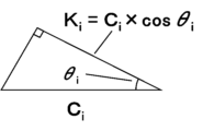
- FIG. 2 is an explanatory diagram of the grain width (Ki) in a columnar crystal grain (i) having a hexagonal crystal structure.
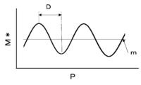
- FIG. 2 is a schematic diagram showing repeated changes in the content of M.
- TiMB composite borides of Ti and elements
- TiMB composite borides of Ti and elements
- TiB2 groups 4 to 6 of the periodic table
- they have found that when TiMB is used as a coating layer for a coated tool, by appropriately controlling the ratio of Ti and M, it is possible to suppress the reactivity with Ti-based alloys while maintaining the hardness inherent to TiB2 , that is, it is possible to achieve both high hardness and adhesion resistance.
- the wear of the coating layer can be suppressed by a structure in which the contents of Ti and M are repeatedly changed in the thickness direction of the coating layer and a structure having a hexagonal columnar crystal structure.
- the surface of a substrate refers to the following. That is, when the substrate has a flat surface like an insert, element mapping is performed using energy dispersive X-ray spectroscopy (EDS) in a longitudinal section (in the case of an insert, a section perpendicular to the substrate surface when the substrate surface is considered to be flat without surface irregularities). Then, the interface between the substrate and the metal boride layer (when there is a lower layer as described below, the lower layer is used instead of the metal boride layer) is represented by a curve based on the difference in shading caused by the difference in elements contained therein, and an average straight line is obtained for this curve, which is the surface of the substrate. Then, the direction perpendicular to this average straight line is the direction perpendicular to the substrate (thickness direction of the coating layer), and the straight line drawn in this perpendicular direction is the perpendicular line.
- EDS energy dispersive X-ray spectroscopy
- the substrate has a curved surface, such as a drill or end mill, if the tool diameter is sufficiently large compared to the thickness of the coating layer, the interface between the coating layer and the substrate in the measurement area will be approximately flat, and the substrate surface can be determined using the same method as when the substrate is flat.
- the longitudinal cross section of the coating layer perpendicular to the axial direction is treated in the same way as when the surface of the base is flat, and this is regarded as the surface of the base.
- the direction perpendicular to this average straight line is regarded as the direction perpendicular to the base (thickness direction of the coating layer).
- the coating layer includes a metal boride layer (TiMB layer).
- TiMB layer metal boride layer
- the average thickness of the TiMB layer is preferably 0.5 to 5.0 ⁇ m. The reason is that if the average thickness is less than 0.5 ⁇ m, it is difficult for the TiMB layer to exhibit wear resistance and chipping resistance over a long period of time, while if the average thickness exceeds 5.0 ⁇ m, the TiMB layer is likely to peel off from the substrate due to residual stress in the TiMB layer, which makes chipping more likely to occur. More preferably, the average thickness of the TiMB layer is 0.5 to 3.0 ⁇ m.
- the average thickness of the TiMB layer is determined by, for example, cutting the coating layer at a vertical cross section at any position using a focused ion beam system (FIB) or a cross section polisher (CP) to prepare a sample for observation, and then observing the vertical cross section with a scanning electron microscope (SEM) (observation magnification, for example, 10,000 to 100,000 times) at multiple locations (e.g., 5 locations) and averaging the thickness measurements.
- FIB focused ion beam system
- CP cross section polisher
- x 0.05 to 0.50 and y is 1.0 to 2.5, where M is one or more of the elements of Groups 4 to 6 of the periodic table, namely Zr, Hf, V, Nb, Ta, Cr, Mo, and W.
- x is less than 0.05, the TiMB layer cannot exhibit sufficient adhesion resistance, whereas if x exceeds 0.50, the hardness of the TiMB layer becomes insufficient. If y is less than 1.0, the TiMB layer will not exhibit sufficient adhesion resistance, whereas if it exceeds 2.5, TiMB will not have a hexagonal crystal structure, the hardness of the TiMB layer will be insufficient, and chipping resistance will decrease. It is more preferable that x is 0.10 to 0.35 and y is 1.7 to 2.3.
- M may contain W.
- the content of W in M may be, for example, 30% or more in atomic ratio, and all of M may be W, that is, 100%.
- W has a particularly low solid solubility in the Ti-based alloy, which is the work material, at high temperatures, and has excellent adhesion resistance and good wear resistance. Furthermore, the addition of W can increase the toughness of the TiMB layer, improving chipping resistance.
- the average composition of the TiMB layer is determined by using an electron probe microanalyzer (EPMA) to irradiate the surface of the coating layer (when there is no surface layer on the coating layer) or multiple locations (e.g., five locations) on a longitudinal section of the coating layer at any position with an electron beam, and quantifying the content of each element by analyzing the characteristic X-rays obtained from each location corresponding to the elements that make up the coating layer, and then calculating the arithmetic average of the results.
- EPMA electron probe microanalyzer
- the TiMB layer has a repeated change in the M content x throughout its thickness direction.
- the change in the content x of M is, for example, as shown in Fig. 4.
- the maximum and minimum values of the content x of M are the same, and the interval between adjacent maximum and minimum values is also the same, but the repeated change of M in this specification and claims means that M repeatedly changes so that it alternates between maximum and minimum values, and the maximum and minimum values may or may not be the same value, and the interval between adjacent maximum and minimum values may or may not be the same.
- the repeated change in the M content occurs because the positional relationship between the target and the substrate surface changes due to the rotation of a table in a high-power pulse sputtering device in one example of the manufacturing method described below.
- the difference ⁇ x between the average value of the maximum value and the average value of the minimum value of x is preferably 0.02 to 0.10.
- the reason for this is that if ⁇ x is 0.02 to 0.10, wear resistance and adhesion resistance are exhibited in the cutting of highly adhesive materials such as Ti-based alloys.
- the maximum and minimum values of x refer to the following:
- the average value of the M content x is a horizontal line (m) that intersects the curve of change in x, and the area above and the area below this average value are equal. Then, the maximum value of x is found in a region in the thickness direction that gives this upper area, and the minimum value of x is found in a region in the thickness direction that gives this lower area.
- the average value of the intervals between the maximum and minimum values i.e., the average value ⁇ of the intervals between the positions in the thickness direction of the coating layer where the maximum value is obtained and the positions in the same direction where the minimum value is obtained (the average value of D in Figure 4), is preferably 2 to 20 nm.
- the reason for this is that if it is shorter than 2 nm, destruction of the coating layer due to wear and cracks that progress in the thickness direction of the coating layer cannot be sufficiently suppressed, while if it exceeds 20 nm, this destruction becomes more likely to progress, resulting in poor wear resistance and a shortened life of the coated cutting tool.
- the maximum and minimum values of x and their average spacing in the thickness direction are determined by analysis using high-angle annular dark field scanning transmission electron microscopy (HAADF-STEM). That is, bright and dark layers are alternately visible throughout the thickness direction of the TiMB layer depending on the difference in composition, and the presence of regions that give an area above the aforementioned average value (bright regions with more M) and regions that give an area below the aforementioned average value (dark regions with less M) is confirmed. Then, using STEM-EDS (Energy Dispersive X-ray Spectroscopy), a composition line analysis is performed in the thickness direction of the TiMB layer over a length spanning at least 20 light and dark regions, and the change in the repeated content of Ti and M is measured. The maximum and minimum values of x are determined, and 10 or more measurement results are averaged to obtain the average value.
- HAADF-STEM high-angle annular dark field scanning transmission electron microscopy
- the TiMB layer may contain columnar crystal grains of hexagonal crystal structure.
- the area ratio is less than 40%, the TiMB layer does not have the wear resistance and chipping resistance required to achieve the above-mentioned objectives, and the higher the area ratio, the more preferable it is, and there is no restriction on the upper limit, so that it may be 100%, i.e., all the crystal grains may be hexagonal columnar crystal grains.
- the hexagonal columnar crystal grains refer to crystal grains having an aspect ratio, which will be described later, of more than 1.0.
- the average crystal grain width of the hexagonal columnar crystal grains is 0.01 to 0.10 ⁇ m. The reason is that if the grain width is less than 0.01 ⁇ m, the grain size is small, the crystal grains are likely to fall off during cutting, and the wear resistance is poor, while if the grain width exceeds 0.10 ⁇ m, the fracture size when fracture such as cracks or fissures in the crystal grains occurs during cutting becomes large, and the wear resistance is poor.
- the average aspect ratio (defined later) is 2.0 to 5.0. The reason for this is that if it is less than 2.0, there will be more granular crystal grains than columnar crystal grains, resulting in poor wear resistance, while if it exceeds 5.0, the size of the breakage will be large if breakage such as cracks or fissures in the crystal grains occurs during cutting, resulting in poor wear resistance.
- the average angle ⁇ between the columnar crystal grains of the hexagonal crystal structure and the perpendicular to the surface of the base is preferably 10 degrees or less. The reason for this is that when the average angle ⁇ is within this range, the crystal grains are less likely to fall off during cutting, and wear is suppressed, and in addition, each crystal grain acts as a shield against the friction loaded on the coating layer surface, making wear less likely to progress and exhibiting excellent wear resistance.
- ACOM automated crystal orientation mapping
- the maximum vertical projection length Vi of the above 1) is the length of a hexagonal columnar crystal grain i projected in a parallel direction when a parallel light beam is applied to the surface of the base, in other words, it is the distance in the direction perpendicular to the surface of the base of a line passing through the closest point and the farthest point on the base among lines that are horizontal to the surface of the base and cross the hexagonal columnar crystal grain i
- the maximum horizontal projection length Li of the above 2) is the length projected in a direction perpendicular to the surface of the base when a parallel light beam is applied to the hexagonal columnar crystal grain i from the direction perpendicular to the surface of the base, in other words, it is the distance in a direction parallel to the surface of the base of a straight line passing through the leftmost point and the rightmost point of a straight line perpendicular to the surface of the base that crosses the hexagonal columnar crystal grain i
- the maximum horizontal crossing length Ci in 3) above is the maximum length that a straight line parallel to the surface
- a right-angled triangle is drawn whose hypotenuse has a maximum horizontal transverse length Ci and has an angle of ⁇ i.
- the average grain width (K) is calculated using Equation 1.
- a lower layer containing a Ti compound (not limited to a stoichiometric compound) layer having a total average thickness of 0.1 to 2.0 ⁇ m and consisting of one or more layers selected from a Ti carbide layer, a nitride layer, a carbonitride layer, a carbonate layer and a carbonitride oxide layer may be provided adjacent to the substrate and separate from the coating layer, in addition to the TiMB layer.
- the lower layer enhances the adhesion between the coating layer and the substrate.
- the upper layer may be provided on the outermost surface (tool surface) of the TiMB layer on the tool surface side.
- An example of the upper layer is a TiN layer. Since the TiN layer has a golden color tone, it can be used as an identification layer to determine whether the coated tool is unused or used based on a color change on the surface of the coated tool.
- the average thickness of the TiN layer serving as the discrimination layer may be, for example, 0.1 to 1.0 ⁇ m.
- the films are formed so that there are no layers other than the TiMB layer, the underlayer, and the upper layer.
- pressure changes and temperature fluctuations may occur unintentionally in the film forming apparatus, and a layer with a different composition from these layers may be formed accidentally (unintentionally) between these layers.
- This layer is called a layer that may be formed accidentally.
- Material of the substrate Any material that is a conventionally known substrate material can be used as long as it does not hinder the achievement of the above-mentioned object.
- cemented carbide WC-based cemented carbide, including WC, Co, and also including carbonitrides of Ti, Ta, Nb, etc.
- cermet mainly composed of TiC, TiN, TiCN, etc.
- ceramics titanium carbide, silicon carbide, silicon nitride, aluminum nitride, aluminum oxide
- cBN sintered body or diamond sintered body.
- the shape of the substrate is not particularly limited as long as it is a shape that can be used as a cutting tool, and examples of the shape include the shapes of an insert, a drill, and an end mill.
- a sputtering method or a high power impulse magnetron sputtering (HiPIMS) method which is easy to suppress the inclusion of droplets, can be used.
- a surface-coated cutting tool having a substrate and a coating layer on the substrate, (a) the coating layer has a boride layer of Ti1- xMxBy (M is one or more of Zr, Hf, V, Nb, Ta , Cr, Mo, and W, x is 0.05 to 0.50, and y is 1.0 to 2.5) having an average thickness of 0.5 to 5.0 ⁇ m; (b) the boride layer has a repeating variation in x throughout its thickness; (c) a difference ⁇ x between the average value of the maximum value of x and the average value of the minimum value of x is 0.02 to 0.10; (d) the average distance ⁇ in the thickness direction between the maximum value of x and the minimum value of x is 2 to 20 nm
- a surface-coated cutting tool comprising: (Appendix 2) 2.
- Appendix 3 3.
- Appendix 4 4.
- the surface-coated cutting tool according to any one of claims 1 to 3, characterized in that columnar crystal grains of a hexagonal structure are present in a longitudinal section of the coating layer, the average grain width K is 0.01 ⁇ m or more and 0.10 ⁇ m or less, the average aspect ratio A is 2.0 or more and 5.0 or less, and the average angle ⁇ between the surface of the base and a perpendicular line is within 10 degrees.
- WC powder (D50: 1.0 ⁇ m), VC powder (D50: 0.8 ⁇ m), TaC powder (D50: 1.5 ⁇ m), NbC powder (D50: 1.5 ⁇ m), Cr3C2 powder (D50: 0.8 ⁇ m), and Co powder (D50: 1.0 ⁇ m ) were prepared and mixed as shown in Table 1.
- the raw material powders were wet mixed in a ball mill for 72 hours, dried, and then pressed into a green compact at a pressure of 100 MPa.
- the green compact was sintered in a vacuum of 6 Pa at a temperature of 1400° C. for 1 hour to produce a round bar sintered compact for forming a cemented carbide substrate with a diameter of 4 mm.
- base bodies (end mills) 1 and 2 made of WC-based cemented carbide and having a four-blade square shape with a cutting edge diameter and length of 2 mm x 4 mm and a twist angle of 40 degrees were produced by grinding.
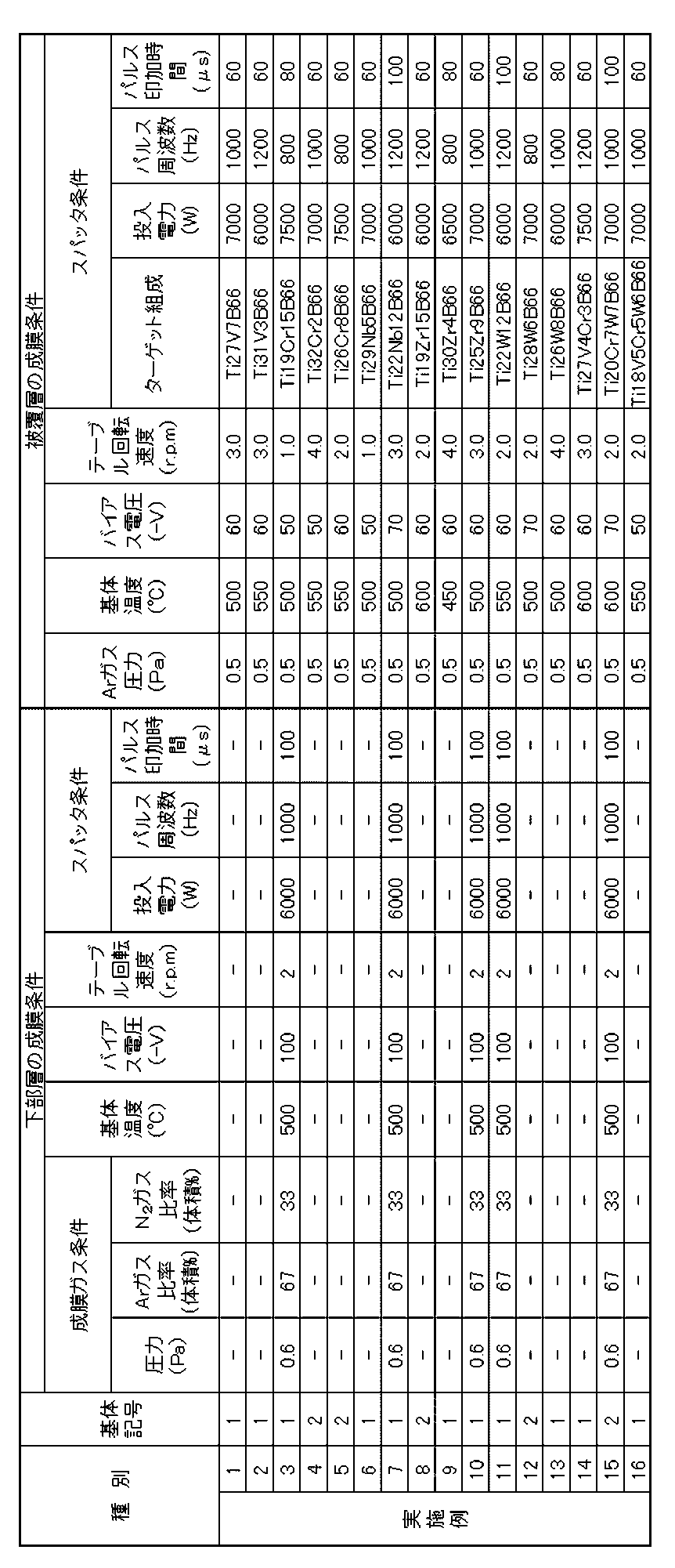
- Each of the substrates 1 and 2 was ultrasonically cleaned in acetone and, in a dried state, mounted along the outer periphery at a position radially away from the central axis on a rotating table in a high-power pulse sputtering device at a predetermined distance. Meanwhile, plate-shaped targets were placed in four locations facing each other across the rotating table in the high-power pulse sputtering device. That is, two opposing sintered targets of Ti, M, and boron, and two opposing Ti metal targets were placed.
- a lower layer and a coating layer were formed on these substrates 1 and 2 under the conditions shown in Table 4 using the procedures (a) to (d) above, and comparative coated end mills (hereinafter referred to as comparative examples) 1 to 7 shown in Table 5 were manufactured.
- a lower layer was not formed on all substrates (a lower layer was formed on comparative examples 5 and 6).
- the cutting length was 150 m (corresponding to a cutting time of 147 minutes), the flank wear width was measured, and the occurrence of chipping was observed.
- Examples 1 to 16 have excellent crack resistance and wear resistance even in the wet cutting test of a Ti-based alloy. In contrast, in Comparative Examples 1 to 7, chipping occurred and the tool life was short.
Landscapes
- Engineering & Computer Science (AREA)
- Mechanical Engineering (AREA)
- Chemical & Material Sciences (AREA)
- Chemical Kinetics & Catalysis (AREA)
- Materials Engineering (AREA)
- Metallurgy (AREA)
- Organic Chemistry (AREA)
- Physical Vapour Deposition (AREA)
- Cutting Tools, Boring Holders, And Turrets (AREA)
Abstract
基体と該基体の上に被覆層を有する表面被覆切削工具であって、 (a)前記被覆層は、0.5~5.0μmの平均厚さのTi1-xMxBy(MはZr、Hf、V、Nb、Ta、Cr、Mo、Wの1種以上、xが0.05~0.50、yが1.0~2.5)の硼化物層を有し、 (b)前記硼化物層は、その厚さ方向の全体にわたって前記xが繰返しの変化を有し、 (c)前記xの極大値の平均値と前記xの極小値の平均値との差Δxが0.02~0.10であって、 (d)前記xの極大値と前記xの極小値の前記厚さ方向平均間隔 Γが2~20nm であることを特徴とする表面被覆切削工具。
Description
この発明は、表面被覆切削工具(以下、被覆工具ということがある)に関する。
従来、超硬合金等を基体とし、この基体の表面に被覆層を蒸着法により形成した被覆工具が知られている。この被覆工具は耐摩耗性を有しているが、この耐摩耗性をさらに向上させるべく、種々の提案がなされ、金属硼化物を含む被覆層に関する提案もなされている。
例えば、特許文献1には、基体表面の中間皮膜を介した被覆層は、Al、Si、Cr、W、Ti、Nb、Zrから選択される1種以上の元素の六方晶構造の硼化物であって、前記中間皮膜は、AlxMyからなる窒化物または炭窒化物(x+y=100、40≦x≦95、5≦y≦60、MはTi、Cr、V、Nbから選択される1種以上)であり、前記基体側が立方晶の結晶構造、前記被覆層側が六方晶の結晶構造である被覆工具が記載され、該被覆工具は耐摩耗性に優れるとされている。
また、例えば、特許文献2には、式W1-xTaxB2-z、または式V1-xWxB2で表され、0.00≦x≦0.45、-0.03≦z≦0.03である硼化物被覆層を有する被覆工具が記載されており、該被覆工具の被覆層は800℃以上の高温において優れた機械特性を有するとされている。
本発明は、前記事情や提案を鑑みてなされたものであって、例えば、Ti基合金のような表面被覆切削工具との溶着性の高い材料を切削加工に供した場合であっても、優れた耐クラック性、耐摩耗性を長期間の使用にわたって発揮する表面被覆切削工具を提供することを目的とする。
本発明の実施形態に係る表面被覆切削工具は、
基体と該基体の上に被覆層を有し、
(a)前記被覆層は、0.5~5.0μmの平均厚さのTi1-xMxBy(MはZr、Hf、V、Nb、Ta、Cr、Mo、Wの1種以上、xが0.05~0.50、yが1.0~2.5)の硼化物層を有し、
(b)前記硼化物層は、その厚さ方向の全体にわたって前記xが繰返しの変化を有し、
(c)前記xの極大値の平均値と前記xの極小値の平均値との差Δxが0.02~0.10であって、
(d)前記xの極大値と前記xの極小値の前記厚さ方向平均間隔Γが2~20nm
である。
基体と該基体の上に被覆層を有し、
(a)前記被覆層は、0.5~5.0μmの平均厚さのTi1-xMxBy(MはZr、Hf、V、Nb、Ta、Cr、Mo、Wの1種以上、xが0.05~0.50、yが1.0~2.5)の硼化物層を有し、
(b)前記硼化物層は、その厚さ方向の全体にわたって前記xが繰返しの変化を有し、
(c)前記xの極大値の平均値と前記xの極小値の平均値との差Δxが0.02~0.10であって、
(d)前記xの極大値と前記xの極小値の前記厚さ方向平均間隔Γが2~20nm
である。
さらに、前記実施形態に係る表面被覆切削工具は、以下の(1)~(3)の事項のいずれか一つ以上を満足してもよい。
(1)前記Mは、Wを必ず含むこと。
(2)前記被覆層の縦断面において六方晶構造の柱状結晶粒が存在し、その面積をShex、それ以外の結晶構造の結晶粒の面積をSothとしたとき、{Shex/(Shex+Soth)}×100が40%以上、100%以下であること。
(2)前記被覆層の縦断面において六方晶構造の柱状結晶粒が存在し、その面積をShex、それ以外の結晶構造の結晶粒の面積をSothとしたとき、{Shex/(Shex+Soth)}×100が40%以上、100%以下であること。
(3)前記被覆層の縦断面において六方晶構造の柱状結晶粒が存在し、その平均結晶粒幅Kが0.01μm以上0.10μm以下であって、平均アスペクト比Aが2.0以上5.0以下であり、前記基体の表面の垂線とのなす角度の平均値θが10度以内であること。
前記の表面被覆工具は、Ti基合金のような表面被覆切削工具との溶着性の高い材料を切削加工に供した場合であっても、優れた耐クラック性、耐摩耗性を長期間の使用にわたって発揮する。
本発明者は、Tiと周期表の4~6族の元素(M)との複合硼化物(以下、「TiMB」ということがある)について鋭意検討した。その結果、TiMBは、被覆工具の被覆層として用いた場合に、TiとMの比率を適切に制御することにより、TiB2が本来有する硬さを維持しながら、Ti基合金に対する反応性を低く抑えることができること、すなわち、高硬度と耐溶着性を両立できることを突き止めた。また、被覆層の厚さ方向に対してTiとMの含有量が繰り返し変化している構造、および六方晶の柱状結晶組織を有する構造により、被覆層の摩耗を抑制できるとの知見を得た。
以下、本発明の実施形態に係る表面被覆切削工具について、説明する。なお、本明細書および特許請求の範囲において数値範囲を「A~B」(A、Bはともに数値である)と表現するとき、その範囲は上限(B)および下限(A)の数値を含んでおり、上限値(B)のみに単位が記載されているとき、上限(B)と下限(A)の単位は同じである。また、数値は測定誤差を含む。
また、本明細書および特許請求の範囲において、基体の表面とは、次のものをいう。
すなわち、基体がインサートのようなその表面が平面のときは、縦断面(インサートでは、基体の表面の凹凸をないものとして基体の表面を平面と考えたときの基体の表面に垂直な断面)においてエネルギー分散型X線分析法(EDS:Energy dispersive X-ray spectroscopy)を用いた元素マッピングを実施する。そして、基体と金属硼化物層(後述する下部層があるときは金属硼化物層の代わりに下部層とする)に含まれる元素の違いに起因する濃淡差から両者の界面を曲線により表し、この曲線に対して平均直線を求めこれを基体の表面とする。そして、この平均直線に対して、垂直な方向を基体に垂直な方向(被覆層の厚さ方向)、この垂直な方向に引いた直線を垂線とする。
すなわち、基体がインサートのようなその表面が平面のときは、縦断面(インサートでは、基体の表面の凹凸をないものとして基体の表面を平面と考えたときの基体の表面に垂直な断面)においてエネルギー分散型X線分析法(EDS:Energy dispersive X-ray spectroscopy)を用いた元素マッピングを実施する。そして、基体と金属硼化物層(後述する下部層があるときは金属硼化物層の代わりに下部層とする)に含まれる元素の違いに起因する濃淡差から両者の界面を曲線により表し、この曲線に対して平均直線を求めこれを基体の表面とする。そして、この平均直線に対して、垂直な方向を基体に垂直な方向(被覆層の厚さ方向)、この垂直な方向に引いた直線を垂線とする。
また、基体がドリル、エンドミルのように曲面の表面を有する場合であっても、被覆層の厚さに対して工具径が十分に大きければ、測定領域における被覆層と基体との間の界面は略平面となることから、基体が平面のときと同様の手法により基体の表面を決定することができる。
すなわち、例えばドリル、エンドミルであれば、軸方向に垂直な断面の被覆層の縦断面において、基体の表面が平面であるときと同じ処理を行い、これを基体の表面とする。そして、この平均直線に対して、垂直な方向を基体に垂直な方向(被覆層の厚さ方向)とする。
1.被覆層
被覆層は、金属硼化物層(TiMB層)を含む。以下、このTiMB層について説明する。
被覆層は、金属硼化物層(TiMB層)を含む。以下、このTiMB層について説明する。
(1)平均厚さ
TiMB層の平均厚さは、0.5~5.0μmであることが好ましい。その理由は、平均厚さが、0.5μm未満であると、TiMB層が長期にわたって耐摩耗性、耐欠損性を発揮することが難しく、一方、5.0μmを超えると、TiMB層が有する残留応力によってTiMB層が基体から剥離しやすくなって、チッピングが発生しやすくなるためである。
TiMB層の平均厚さは、0.5~3.0μmであることがより好ましい。
TiMB層の平均厚さは、0.5~5.0μmであることが好ましい。その理由は、平均厚さが、0.5μm未満であると、TiMB層が長期にわたって耐摩耗性、耐欠損性を発揮することが難しく、一方、5.0μmを超えると、TiMB層が有する残留応力によってTiMB層が基体から剥離しやすくなって、チッピングが発生しやすくなるためである。
TiMB層の平均厚さは、0.5~3.0μmであることがより好ましい。
なお、TiMB層の平均厚さは、例えば、集束イオンビーム装置(FIB:Focused Ion Beam system)、クロスセクションポリッシャー装置(CP:Cross section Polisher)等を用いて、被覆層を任意の位置の縦断面で切断して観察用の試料を作製し、その縦断面を走査型電子顕微鏡(Scanning Electron Microscope:SEM)を用いた観察(観察倍率は、例えば、1万から10万倍)により複数箇所(例えば、5箇所)の厚さの測定結果を平均したものである。
(2)平均組成
TiMB層の平均組成は、式:Ti1-xMxByで表したとき、xは0.05~0.50、yは1.0~2.5を満足することが好ましい。ただし、Mは周期表の4~6族の元素の中のZr、Hf、V、Nb、Ta、Cr、Mo、Wの1種以上である。
ただし、Mが2種以上のとき、すなわち、M=M1、M2、・・・、Mn(2≦n≦8)であるとき、
Mi(i=1~n)の含有量をxiとすると、x=x1+x2+…+xnとなる。
TiMB層の平均組成は、式:Ti1-xMxByで表したとき、xは0.05~0.50、yは1.0~2.5を満足することが好ましい。ただし、Mは周期表の4~6族の元素の中のZr、Hf、V、Nb、Ta、Cr、Mo、Wの1種以上である。
ただし、Mが2種以上のとき、すなわち、M=M1、M2、・・・、Mn(2≦n≦8)であるとき、
Mi(i=1~n)の含有量をxiとすると、x=x1+x2+…+xnとなる。
x、yを前記範囲とした理由は、次のとおりである。
xが、0.05未満であるとTiMB層の十分な耐溶着性が発揮できず、一方、0.50を超えると、TiMB層の硬さが不十分となる。
yが、1.0未満であるとTiMB層の十分な耐溶着性が発揮できず、一方、2.5を超えるとTiMBが六方晶構造とはならず、TiMB層の硬さが不十分となり、耐チッピング性が低下する。
xは0.10~0.35、yは1.7~2.3であることがより好ましい。
xが、0.05未満であるとTiMB層の十分な耐溶着性が発揮できず、一方、0.50を超えると、TiMB層の硬さが不十分となる。
yが、1.0未満であるとTiMB層の十分な耐溶着性が発揮できず、一方、2.5を超えるとTiMBが六方晶構造とはならず、TiMB層の硬さが不十分となり、耐チッピング性が低下する。
xは0.10~0.35、yは1.7~2.3であることがより好ましい。
Mとして、Wを含むことがある。また、Mとして他の元素が含有される場合に、Mの中のWの含有量は原子比で例えば、30%以上であってよく、Mの全てがW、すなわち、100%であってもよい。
周期表4~6族元素の中でWは、特に、被削材であるTi基合金に対する高温中の固溶度が低く、優れた耐溶着性を有すると共に耐摩耗性も良好である。また、Wを添加することによりTiMB層のより靭性を増すことができ、耐チッピング性が向上する。
周期表4~6族元素の中でWは、特に、被削材であるTi基合金に対する高温中の固溶度が低く、優れた耐溶着性を有すると共に耐摩耗性も良好である。また、Wを添加することによりTiMB層のより靭性を増すことができ、耐チッピング性が向上する。
TiMB層の平均組成は、電子線マイクロアナライザ(EPMA:Electron Probe Micro Analyzer)を用い、電子線を被覆層の表面(被覆層上に表面層がないとき)、もしくは、被覆層の任意の位置の縦断面の複数箇所(例えば、5箇所)に照射し、それぞれの箇所から得られた被覆層を構成する元素に対応する特性X線を解析することにより各元素の含有量の定量化を行い、その結果を算術平均して求める。
(3)厚さ方向のMの含有量の変化
TiMB層は、その厚さ方向の全体にわたってMの含有量xが繰返し変化を有することが好ましい。
Mの含有量xの変化は、例えば、図4に模式的に示されるものである。図4では、Mの含有量xの極大値、極小値のそれぞれが同じ値であり、隣接する極大値と極小値の間隔も同じであるが、本明細書および特許請求の範囲でいうMの繰返し変化とは、Mが極大値と極小値を交互にとるように繰り返して変化すればよく、極大値及び極小値がそれぞれ同じ値であっても同じ値でなくてもよく、隣接する極大値と極小値との間隔も同じであっても異なっていてもよい。
Mの含有量の繰返し変化は、後述する製造方法の一例では高出力パルススパッタリング装置内のテーブル回転によりターゲットと基材表面との位置関係が変化するために生じる。
TiMB層は、その厚さ方向の全体にわたってMの含有量xが繰返し変化を有することが好ましい。
Mの含有量xの変化は、例えば、図4に模式的に示されるものである。図4では、Mの含有量xの極大値、極小値のそれぞれが同じ値であり、隣接する極大値と極小値の間隔も同じであるが、本明細書および特許請求の範囲でいうMの繰返し変化とは、Mが極大値と極小値を交互にとるように繰り返して変化すればよく、極大値及び極小値がそれぞれ同じ値であっても同じ値でなくてもよく、隣接する極大値と極小値との間隔も同じであっても異なっていてもよい。
Mの含有量の繰返し変化は、後述する製造方法の一例では高出力パルススパッタリング装置内のテーブル回転によりターゲットと基材表面との位置関係が変化するために生じる。
このxの極大値の平均値と極小値の平均値との差Δxが0.02~0.10であることが好ましい。その理由は、Δxが0.02~0.10であれば、Ti基合金等の溶着性の高い材料の切削加工において、耐摩耗性および耐溶着性が発揮される。
ここで、xの極大値および極小値とは、次のものをいう。
図4において、Mの含有量xの平均値とは、xの変化曲線を横切る水平線(m)であって、この平均値よりも上方の面積と下方の面積が等しくなるものである。
そして、この上方の面積を与える厚さ方向の領域においてxの極大値を求め、この下方の面積を与える厚さ方向の領域においてxの極小値を求める。
図4において、Mの含有量xの平均値とは、xの変化曲線を横切る水平線(m)であって、この平均値よりも上方の面積と下方の面積が等しくなるものである。
そして、この上方の面積を与える厚さ方向の領域においてxの極大値を求め、この下方の面積を与える厚さ方向の領域においてxの極小値を求める。
また、極大値と極小値を与える間隔の平均値、すなわち、極大値を与える被覆層の厚さ方向の位置と極小値を与える同方向の位置との間隔の平均値Γ(図4のDの平均値)は、2~20nmであることが好ましい。その理由は、2nmより短いと、被覆層の厚さ方向に進展する摩耗やクラック等による被覆層の破壊を十分に抑制できず、一方、20nm超えるとこの破壊が進展しやすくなり、耐摩耗性に劣り、被覆切削工具の寿命が短くなるためである。
前記xの極大値と極小値およびその厚さ方向の平均間隔は、高角散乱環状暗視野走査透過顕微鏡法(HAADF-STEM:High-Angle Annular Dark Field Scanning Transmission Electron Microscopy)を用いた解析によって求める。すなわち、TiMB層の厚さ方向全体にわたって組成の違いに応じて明るい層と暗い層が交互に視認されるので、前述の平均値よりも上方の面積を与える領域(明るい領域でMが多い)と前述の平均値よりも下方の面積を与える領域(暗い領域でMが少ない)の存在を確認する。そして、STEM-EDS(Energy Dispersive X-ray Spectrpscopy)を用いてTiMB層の厚さ方向に明暗の領域を少なくとも20個を跨ぐ長さで組成ライン分析を行い、TiとMの繰返しの含有量の変化を測定する。xの極大値と極小値をそれぞれ求め、それぞれ、10以上の測定結果を平均してこれらの平均値とする。
(4)六方晶構造の柱状結晶粒
TiMB層には、六方晶構造の柱状結晶粒が存在してもよい。
TiMB層には、六方晶構造の柱状結晶粒が存在してもよい。
(4-1)面積率
TiMB層の任意の縦断面において、六方晶構造の柱状結晶粒(六方晶柱状晶粒ということがある)の面積をShex、それ以外の結晶構造の結晶粒の面積をSothとしたとき、{Shex/(Shex+Soth)}×100により定義される面積割合が40%以上、100%以下である。
TiMB層の任意の縦断面において、六方晶構造の柱状結晶粒(六方晶柱状晶粒ということがある)の面積をShex、それ以外の結晶構造の結晶粒の面積をSothとしたとき、{Shex/(Shex+Soth)}×100により定義される面積割合が40%以上、100%以下である。
その理由は、面積割合が40%未満であると、TiMB層が前述の目的を達成するために必要な耐摩耗性、耐チッピング性を有しない。この面積割合は高い方が好ましく、上限は制約がなく100%、すなわち、すべての結晶粒が六方晶柱状晶粒であってもよい。
ここで、六方晶柱状晶粒とは、後述するアスペクト比が1.0を超えるものをいう。
ここで、六方晶柱状晶粒とは、後述するアスペクト比が1.0を超えるものをいう。
(4-2)結晶粒幅と平均アスペクト比
六方晶柱状晶粒の平均結晶粒幅は、0.01~0.10μmである。その理由は、0.01μm未満であると粒径が小さく、切削中に結晶粒が脱落しやすく、耐摩耗性に劣り、一方、0.10μmを超えると切削中に結晶粒の亀裂やクラック等の破壊が発生したときの破壊サイズが大きくなり、耐摩耗性が劣るためである。
六方晶柱状晶粒の平均結晶粒幅は、0.01~0.10μmである。その理由は、0.01μm未満であると粒径が小さく、切削中に結晶粒が脱落しやすく、耐摩耗性に劣り、一方、0.10μmを超えると切削中に結晶粒の亀裂やクラック等の破壊が発生したときの破壊サイズが大きくなり、耐摩耗性が劣るためである。
また、平均アスペクト比(定義は後述する)は、2.0~5.0である。その理由は、2.0未満であると、柱状の結晶粒よりも粒状の結晶粒が多くなって耐摩耗性が劣り、一方、5.0を超えると切削中に結晶粒の亀裂やクラック等の破壊が発生した場合の破壊サイズが大きくなり、耐摩耗性が劣るためである。
(4-3)基体の表面の垂線となす角度
六方晶構造の柱状結晶粒が基体の表面の垂線となす角度の平均値θが10度以下がよい。その理由は、角度の平均値θがこの範囲にあると、切削中に結晶粒が脱落しづらく、損耗が抑制されることに加え、被覆層表面に負荷される摩擦に対して各々の結晶粒が盾の役割を果たすため摩耗が進行し辛く、優れた耐摩耗性を発揮するためである。
六方晶構造の柱状結晶粒が基体の表面の垂線となす角度の平均値θが10度以下がよい。その理由は、角度の平均値θがこの範囲にあると、切削中に結晶粒が脱落しづらく、損耗が抑制されることに加え、被覆層表面に負荷される摩擦に対して各々の結晶粒が盾の役割を果たすため摩耗が進行し辛く、優れた耐摩耗性を発揮するためである。
(4-4)測定方法
結晶構造ごとの面積割合、結晶粒幅とアスペクト比、および、基体の表面の垂線となす角度の測定は、結晶粒界の画定を行って、次のように測定する。
結晶構造ごとの面積割合、結晶粒幅とアスペクト比、および、基体の表面の垂線となす角度の測定は、結晶粒界の画定を行って、次のように測定する。
<1>結晶粒界の画定
透過型電子顕微鏡(TEM:Transmission Electron Microscope)による、自動結晶方位マッピング(ACOM:Automated Crystal Orientation Mapping)-TEMを用いた被覆層の任意の縦断面の解析を行い、六方晶柱状晶粒iの結晶粒界を画定する。
ここで、例えば、解析範囲は、縦(被覆層の厚さ方向):1.0μm、横(基体に平行な方向):0.5μm、スキャン間隔は2nmとし、iは六方晶柱状晶粒を区別する番号で、i=1~Nであり、Nは測定対象となる六方晶柱状晶粒の総数であって、その値が20以上となるように選ぶ。なお、前記解析範囲内では、Nの値が20以上とならないときは、同じ大きさの解析範囲をNの値が20以上になるまで増やす。
透過型電子顕微鏡(TEM:Transmission Electron Microscope)による、自動結晶方位マッピング(ACOM:Automated Crystal Orientation Mapping)-TEMを用いた被覆層の任意の縦断面の解析を行い、六方晶柱状晶粒iの結晶粒界を画定する。
ここで、例えば、解析範囲は、縦(被覆層の厚さ方向):1.0μm、横(基体に平行な方向):0.5μm、スキャン間隔は2nmとし、iは六方晶柱状晶粒を区別する番号で、i=1~Nであり、Nは測定対象となる六方晶柱状晶粒の総数であって、その値が20以上となるように選ぶ。なお、前記解析範囲内では、Nの値が20以上とならないときは、同じ大きさの解析範囲をNの値が20以上になるまで増やす。
<2>六方晶柱状晶粒iの大きさの測定
結晶粒界を画定し六方晶柱状晶粒iを特定したら、その六方晶柱状晶粒の大きさを測定する。
すなわち、図1に示すように、六方晶柱状晶粒iについて、
1)最大垂直投影長さVi
2)最大水平投影長さLi
3)最大水平横断長さCi
を測定する。
結晶粒界を画定し六方晶柱状晶粒iを特定したら、その六方晶柱状晶粒の大きさを測定する。
すなわち、図1に示すように、六方晶柱状晶粒iについて、
1)最大垂直投影長さVi
2)最大水平投影長さLi
3)最大水平横断長さCi
を測定する。
ここで、
前記1)の最大垂直投影長さViとは、六方晶柱状晶粒iに対して、基体の表面に平行な方向から平行光線をあて、この平行な方向へ投影される長さであり、換言すると、基体の表面に対する水平な直線で六方晶柱状晶粒iを横断する直線のうち、基体に最も近い点と最も遠い点をそれぞれ通る直線の基体の表面に垂直な方向の距離であり、
前記2)の最大水平投影長さLiとは、六方晶柱状晶粒iに対して、基体の表面に垂直な方向から平行光線をあて、この垂直な方向へ投影される長さであり、換言すると、基体の表面に対する垂直な直線で六方晶柱状晶粒iを横断する直線のうち、最も左にある点と、最も右側の点をそれぞれ通る直線の基体の表面に平行な方向の距離であり、
前記3)の最大水平横断長さCiとは、基体の表面に平行な直線が六方晶柱状晶粒iを横断するとき、その横断する長さの最大長さである。
前記1)の最大垂直投影長さViとは、六方晶柱状晶粒iに対して、基体の表面に平行な方向から平行光線をあて、この平行な方向へ投影される長さであり、換言すると、基体の表面に対する水平な直線で六方晶柱状晶粒iを横断する直線のうち、基体に最も近い点と最も遠い点をそれぞれ通る直線の基体の表面に垂直な方向の距離であり、
前記2)の最大水平投影長さLiとは、六方晶柱状晶粒iに対して、基体の表面に垂直な方向から平行光線をあて、この垂直な方向へ投影される長さであり、換言すると、基体の表面に対する垂直な直線で六方晶柱状晶粒iを横断する直線のうち、最も左にある点と、最も右側の点をそれぞれ通る直線の基体の表面に平行な方向の距離であり、
前記3)の最大水平横断長さCiとは、基体の表面に平行な直線が六方晶柱状晶粒iを横断するとき、その横断する長さの最大長さである。
<3>測定長さの換算
前記<2>で測定した1)最大垂直投影長さVi、2)最大水平投影長さLi、および、3)最大水平横断長さCiから、
4)六方晶柱状晶粒iの長さHi
5)六方晶柱状晶粒iの幅Ki
を算出する。
前記<2>で測定した1)最大垂直投影長さVi、2)最大水平投影長さLi、および、3)最大水平横断長さCiから、
4)六方晶柱状晶粒iの長さHi
5)六方晶柱状晶粒iの幅Ki
を算出する。
すなわち、図2に示すように、辺の長さが、最大垂直投影長さViと最大水平投影長さLiとなる四角形を作図し、その対角線と最大垂直投影長さViを与える辺となす角度θiを求め、
前記4)六方晶柱状晶粒の長さHiを、
六方晶柱状晶粒の長さHi=Vi/cosθi
により算出する。
前記4)六方晶柱状晶粒の長さHiを、
六方晶柱状晶粒の長さHi=Vi/cosθi
により算出する。
また、図3に示すように、斜辺の長さが最大水平横断長さCiであり、前記θiの角度を有する直角三角形を作図し、
前記5)六方晶柱状晶粒iの幅Kiを、
六方晶柱状晶粒iの幅Ki=Ci×cosθi
により算出する。
前記5)六方晶柱状晶粒iの幅Kiを、
六方晶柱状晶粒iの幅Ki=Ci×cosθi
により算出する。
<4>平均結晶粒幅と平均アスペクト比
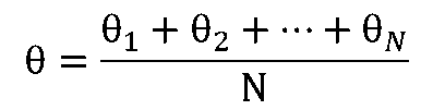
六方晶柱状結晶粒iのアスペクト比(Ai)をAi=Hi/Kiとし、アスペクト比が1.0を超える六方晶柱状結晶粒iに対して、以下のようにして平均結晶粒幅(K)、平均アスペクト比(A)、θi平均値(θ)を求める。
六方晶柱状結晶粒iのアスペクト比(Ai)をAi=Hi/Kiとし、アスペクト比が1.0を超える六方晶柱状結晶粒iに対して、以下のようにして平均結晶粒幅(K)、平均アスペクト比(A)、θi平均値(θ)を求める。
平均結晶粒幅(K)は、[数1]によって、求める。

また、アスペクト比(Ai=Hi/Ki)と面積(Si=Hi×Kiとして、平均アスペクト比Aを[数2]により求める。

さらに、θiの平均値(θ)を[数3]により求める。
2.その他の層
(1)下部層
被覆層として、TiMB層とは別に、Tiの炭化物層、窒化物層、炭窒化物層、炭酸化物層および炭窒酸化物層のうちの1層または2層以上からなり、0.1~2.0μmの合計平均厚さを有するTi化合物(化学量論的な化合物に限定されない)層を含む下部層を基体に隣接して被覆層とは別に設けてもよい。下部層は被覆層と基体の密着性を高める。
(1)下部層
被覆層として、TiMB層とは別に、Tiの炭化物層、窒化物層、炭窒化物層、炭酸化物層および炭窒酸化物層のうちの1層または2層以上からなり、0.1~2.0μmの合計平均厚さを有するTi化合物(化学量論的な化合物に限定されない)層を含む下部層を基体に隣接して被覆層とは別に設けてもよい。下部層は被覆層と基体の密着性を高める。
(2)上部層
上部層は、TiMB層の工具表面側の最表面(工具表面)に設けてもよい。上部層は、TiN層が例示できる。TiN層が黄金色の色調を有することから、例えば、被覆工具が未使用であるか使用されたものであるかを被覆工具表面の色調変化によって、判別する識別層とすることができる。
なお、この識別層としてのTiN層の平均厚みは、例えば、0.1~1.0μmでよい。
上部層は、TiMB層の工具表面側の最表面(工具表面)に設けてもよい。上部層は、TiN層が例示できる。TiN層が黄金色の色調を有することから、例えば、被覆工具が未使用であるか使用されたものであるかを被覆工具表面の色調変化によって、判別する識別層とすることができる。
なお、この識別層としてのTiN層の平均厚みは、例えば、0.1~1.0μmでよい。
(3)偶発的に生じる可能性のある層
本実施形態では、TiMB層、下地層および上部層以外は存在しないように成膜される。しかし、成膜すべき層の種類を変更する際に、成膜装置内の圧力変化や温度の変動が意図せずに発生することがあり、これら層とは組成の異なった層がこれらの層の間に(意図せずに)偶発的に形成されることがある。この層のことを偶発的に生じる可能性のある層という。
本実施形態では、TiMB層、下地層および上部層以外は存在しないように成膜される。しかし、成膜すべき層の種類を変更する際に、成膜装置内の圧力変化や温度の変動が意図せずに発生することがあり、これら層とは組成の異なった層がこれらの層の間に(意図せずに)偶発的に形成されることがある。この層のことを偶発的に生じる可能性のある層という。
3.基体
(1)材質
材質は、従来公知の基体の材質であれば、前述の目的を達成することを阻害するものでない限り、いずれのものも使用可能である。一例をあげるならば、超硬合金(WC基超硬合金、WCの他、Coを含み、さらに、Ti、Ta、Nb等の炭窒化物を添加したものも含むもの)、サーメット(TiC、TiN、TiCN等を主成分とするもの)、セラミックス(炭化チタン、炭化珪素、窒化珪素、窒化アルミニウム、酸化アルミニウム)、cBN焼結体、またはダイヤモンド焼結体のいずれかである。
(1)材質
材質は、従来公知の基体の材質であれば、前述の目的を達成することを阻害するものでない限り、いずれのものも使用可能である。一例をあげるならば、超硬合金(WC基超硬合金、WCの他、Coを含み、さらに、Ti、Ta、Nb等の炭窒化物を添加したものも含むもの)、サーメット(TiC、TiN、TiCN等を主成分とするもの)、セラミックス(炭化チタン、炭化珪素、窒化珪素、窒化アルミニウム、酸化アルミニウム)、cBN焼結体、またはダイヤモンド焼結体のいずれかである。
(2)形状
基体の形状は、切削工具として用いられる形状であれば特段の制約はなく、インサートの形状、ドリル、エンドミルの形状が例示できる。
基体の形状は、切削工具として用いられる形状であれば特段の制約はなく、インサートの形状、ドリル、エンドミルの形状が例示できる。
4.製造方法
例えば、スパッタンリング法または混入液滴の抑制が容易な大電力パルススパッタリング(High Power Impulse Magnetron Sputtering:HiPIMS)法を用いることができる。
例えば、スパッタンリング法または混入液滴の抑制が容易な大電力パルススパッタリング(High Power Impulse Magnetron Sputtering:HiPIMS)法を用いることができる。
以上の説明は、以下に付記する特徴を含む。
(付記1)
基体と該基体の上に被覆層を有する表面被覆切削工具であって、
(a)前記被覆層は、0.5~5.0μmの平均厚さのTi1-xMxBy(MはZr、Hf、V、Nb、Ta、Cr、Mo、Wの1種以上、xが0.05~0.50、yが1.0~2.5)の硼化物層を有し、
(b)前記硼化物層は、その厚さ方向の全体にわたって前記xが繰返しの変化を有し、
(c)前記xの極大値の平均値と前記xの極小値の平均値との差Δxが0.02~0.10であって、
(d)前記xの極大値と前記xの極小値の前記厚さ方向平均間隔 Γが2~20nm
であることを特徴とする表面被覆切削工具。
(付記2)
前記Mは、Wを必ず含むことを特徴とする付記1に記載の表面被覆切削工具。
(付記3)
前記被覆層の縦断面において六方晶構造の柱状結晶粒が存在し、その面積をShex、それ以外の結晶構造の結晶粒の面積をSothとしたとき、{Shex/(Shex+Soth)}×100が40%以上、100%以下であることを特徴とする付記1または2に記載の表面被覆切削工具。
(付記4)
前記被覆層の縦断面において六方晶構造の柱状結晶粒が存在し、その平均粒幅Kが0.01μm以上0.10μm以下であって、平均アスペクト比Aが2.0以上5.0以下であり、前記基体の表面の垂線とのなす角度の平均値θが10度以内であることを特徴とする付記1~3のいずれかに記載の表面被覆切削工具。
(付記1)
基体と該基体の上に被覆層を有する表面被覆切削工具であって、
(a)前記被覆層は、0.5~5.0μmの平均厚さのTi1-xMxBy(MはZr、Hf、V、Nb、Ta、Cr、Mo、Wの1種以上、xが0.05~0.50、yが1.0~2.5)の硼化物層を有し、
(b)前記硼化物層は、その厚さ方向の全体にわたって前記xが繰返しの変化を有し、
(c)前記xの極大値の平均値と前記xの極小値の平均値との差Δxが0.02~0.10であって、
(d)前記xの極大値と前記xの極小値の前記厚さ方向平均間隔 Γが2~20nm
であることを特徴とする表面被覆切削工具。
(付記2)
前記Mは、Wを必ず含むことを特徴とする付記1に記載の表面被覆切削工具。
(付記3)
前記被覆層の縦断面において六方晶構造の柱状結晶粒が存在し、その面積をShex、それ以外の結晶構造の結晶粒の面積をSothとしたとき、{Shex/(Shex+Soth)}×100が40%以上、100%以下であることを特徴とする付記1または2に記載の表面被覆切削工具。
(付記4)
前記被覆層の縦断面において六方晶構造の柱状結晶粒が存在し、その平均粒幅Kが0.01μm以上0.10μm以下であって、平均アスペクト比Aが2.0以上5.0以下であり、前記基体の表面の垂線とのなす角度の平均値θが10度以内であることを特徴とする付記1~3のいずれかに記載の表面被覆切削工具。
次に、実施例について説明するが、本発明はこれら実施例に限定されるものではない。
原料粉末として、WC粉末(D50:1.0μm)、VC粉末(D50:0.8μm)、TaC粉末(D50:1.5μm)、NbC粉末(D50:1.5μm)、Cr3C2粉末(D50:0.8μm)、およびCo粉末(D50:1.0μm)を用意し、これら原料粉末を、表1に示されたように配合した。ボールミルで72時間湿式混合し、乾燥した後、100MPaの圧力で圧粉体にプレス成形し、この圧粉体を6Paの真空中、温度:1400℃に1時間保持の条件で焼結し、直径が4mmの超硬基体形成用丸棒焼結体を作製した。さらに、この丸棒焼結体から、研削加工にて、切刃部の直径×長さがそれぞれ2mm×4mm、ねじれ角40度の4枚刃スクエア形状を持ったWC基超硬合金製の基体(エンドミル)1および2を製造した。
(a)前記基体1、2のそれぞれを、アセトン中で超音波洗浄し、乾燥した状態で、高出力パルススパッタリング装置内の回転テーブル上の中心軸から半径方向に所定距離離れた位置に外周部に沿って装着した。一方、高出力パルススパッタリング装置内には、回転テーブルを挟んで対向する4か所に板状のターゲットを設置した。すなわち、対向しあう2個のTiとMと硼素の焼結体ターゲット、および、対向しあう2個のTi金属ターゲットを配置した。
(b)前記装置内を排気して0.1Pa以下の真空に保持しながら、ヒーターで装置内を500℃に加熱した後、前記回転テーブル上で自転する基体に-200Vの直流バイアス電圧を印加した後、前記装置内へ放電・スパッタ用ガスとしてアルゴン(以下Arと表記する)ガスを導入し、2.0Paの雰囲気とした。さらに前記装置内に具備されるタングステンフィラメントへ40Aの電流を流すことによりArイオンを励起させ、前記基体を1時間、Arボンバード処理した。
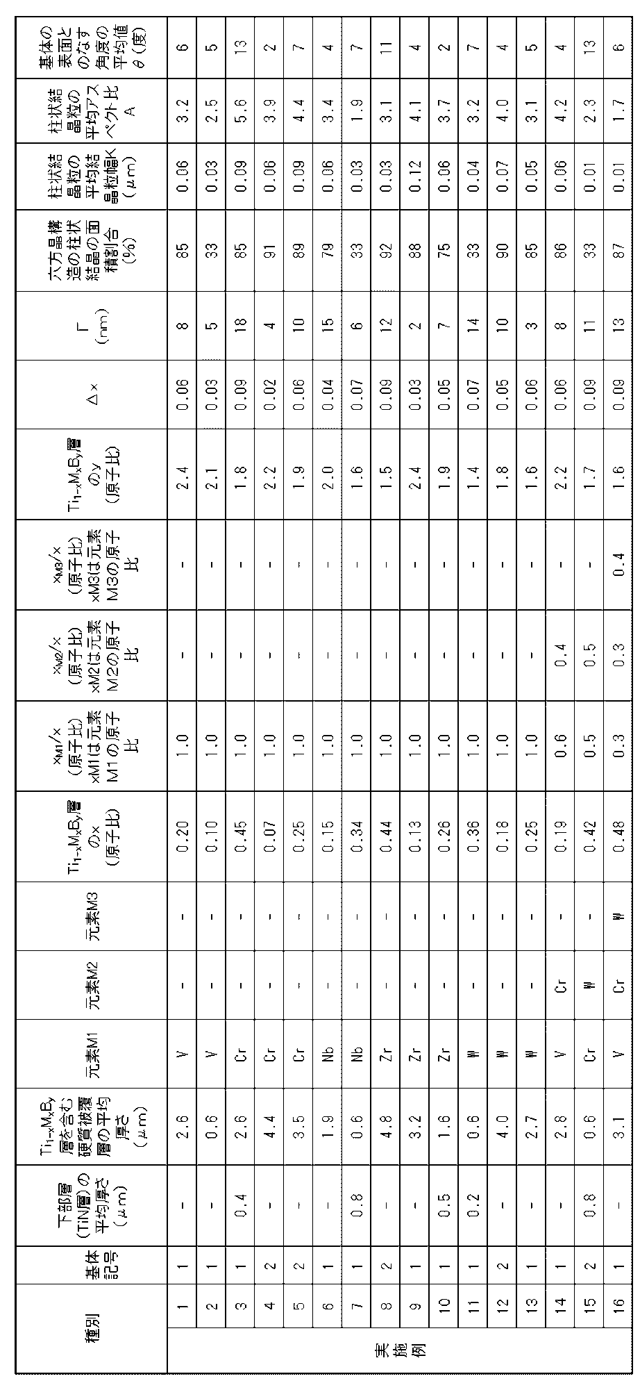
(c)前記装置内にスパッタ用ガスとしてArガスと反応ガスとしての窒素ガスとを導入して0.6Paの反応雰囲気とすると共に、前記金属Tiターゲットを用いて表2に示される所定のパルススパッタ条件で高出力パルススパッタを行い、これにより前記基体の表面に、表3に示される平均厚さのTiN層を被覆層の下部層として成膜した。ただし、すべての基体に下部層を形成したわけではない(後述する実施例3、7、10、11、および15に下部層を成膜した)。
(d)引き続き、装置内に導入するガスのうち窒素ガスを閉じると共に、装置内雰囲気を0.5Paとし、十分に窒素ガスの排出がなされ、Arガスのみの装置内雰囲気となった後、TiとMと硼素からなる焼結体ターゲットを用いて表2に示される所定のパルススパッタ条件で、所定時間で高出力パルススパッタを行い、表3に示す本発明被覆エンドミル(以下、実施例という)1~16を製造した。
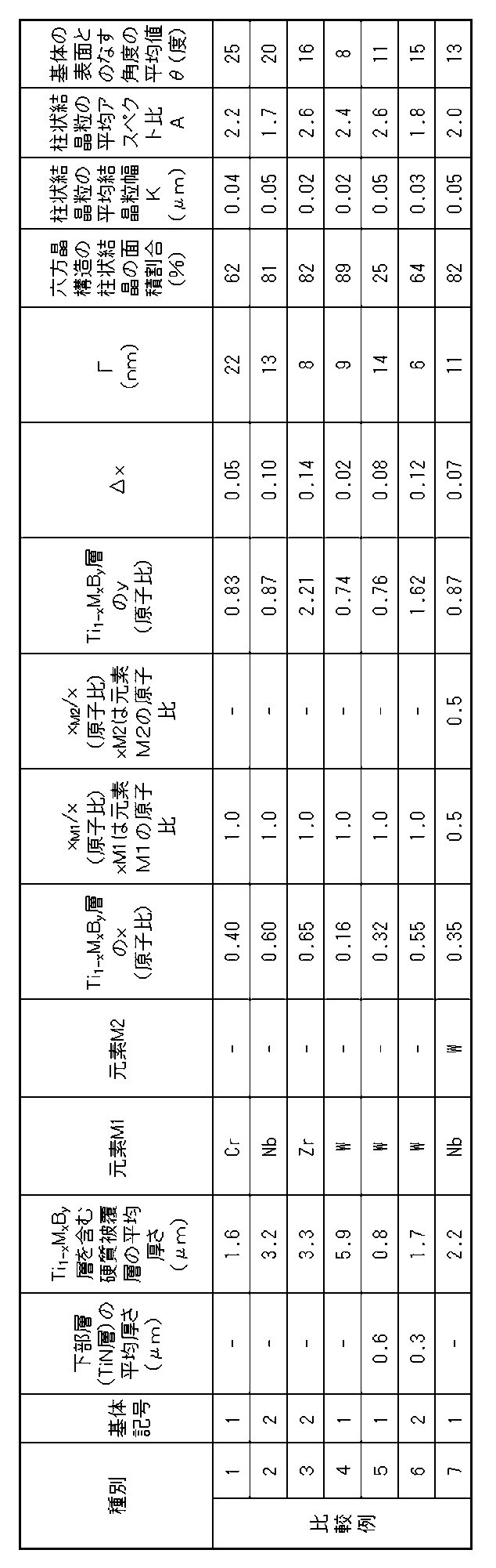
また、比較の目的で、これら基体1~2に対して、表4に示す条件で前記(a)~(d)の手順により下部層と被覆層を形成し、表5に示す比較被覆エンドミル(以下、比較例という)1~7を製造した。ただし、すべての基体に下部層を形成したわけではない(比較例5および6に下部層を成膜した)。
以下の表において、「-」は該当するものがないことを示している。


次に、実施例1~16、比較例1~7に対して、以下の切削試験を行い、その結果を表6に示す。
(切削試験)
被削材:Ti基合金(質量%で、Ti-6%Al-4%V合金)のブロック材
(幅190mm×250mm)
切削速度:80m/min
回転速度:12732min-1
送り速度:1019mm/min
軸方向切込み量(ap):2.0mm
径方向切込み量(ae):0.2mm
エンドミル刃外径:2mm
被削材:Ti基合金(質量%で、Ti-6%Al-4%V合金)のブロック材
(幅190mm×250mm)
切削速度:80m/min
回転速度:12732min-1
送り速度:1019mm/min
軸方向切込み量(ap):2.0mm
径方向切込み量(ae):0.2mm
エンドミル刃外径:2mm
切削長150m(切削時間として147分に相当)まで切削し、逃げ面摩耗幅を測定し、チッピング発生の有無を観察した。
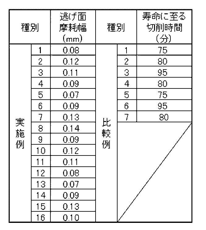
表6において、比較例の寿命に至る切削時間(分)とは、チッピング発生が原因で寿命に至るまでの切削時間(分)を示している。
表6に示す結果から明らかなように、実施例1~16は、Ti基合金の湿式切削試験であっても優れた耐クラック性および耐摩耗性を有していることがわかる。
これに対して、比較例1~7は、チッピングが発生し短時間の工具寿命であった。
これに対して、比較例1~7は、チッピングが発生し短時間の工具寿命であった。
前記開示した実施の形態はすべての点で例示にすぎず、制限的なものではない。本発明の範囲は前記した実施の形態ではなく請求の範囲によって示され、請求の範囲と均等の意味、および範囲内でのすべての変更が含まれることが意図される。
1 六方晶柱状晶粒i
Vi 六方晶柱状晶粒iの最大垂直投影長さ
Li 六方晶柱状晶粒iの最大水平投影長さ
Ci 六方晶柱状晶粒iの最大水平横断長さ
Hi 六方晶柱状晶粒iの長
Ki 六方晶柱状晶粒iの幅
θi 六方晶柱状結晶粒iが基体の表面の垂線となす角度
P 基体表面に垂直方向の位置(厚さ方向の位置)
M* Mの含有量
D 間隔
m 水平線(xの平均値)
Vi 六方晶柱状晶粒iの最大垂直投影長さ
Li 六方晶柱状晶粒iの最大水平投影長さ
Ci 六方晶柱状晶粒iの最大水平横断長さ
Hi 六方晶柱状晶粒iの長
Ki 六方晶柱状晶粒iの幅
θi 六方晶柱状結晶粒iが基体の表面の垂線となす角度
P 基体表面に垂直方向の位置(厚さ方向の位置)
M* Mの含有量
D 間隔
m 水平線(xの平均値)
Claims (4)
- 基体と該基体の上に被覆層を有する表面被覆切削工具であって、
(a)前記被覆層は、0.5~5.0μmの平均厚さのTi1-xMxBy(MはZr、Hf、V、Nb、Ta、Cr、Mo、Wの1種以上、xが0.05~0.50、yが1.0~2.5)の硼化物層を有し、
(b)前記硼化物層は、その厚さ方向の全体にわたって前記xが繰返しの変化を有し、
(c)前記xの極大値の平均値と前記xの極小値の平均値との差Δxが0.02~0.10であって、
(d)前記xの極大値と前記xの極小値の前記厚さ方向平均間隔 Γが2~20nm
であることを特徴とする表面被覆切削工具。 - 前記Mは、Wを必ず含むことを特徴とする請求項1に記載の表面被覆切削工具。
- 前記被覆層の縦断面において六方晶構造の柱状結晶粒が存在し、その面積をShex、それ以外の結晶構造の結晶粒の面積をSothとしたとき、{Shex/(Shex+Soth)}×100が40%以上、100%以下であることを特徴とする請求項1に記載の表面被覆切削工具。
- 前記被覆層の縦断面において六方晶構造の柱状結晶粒が存在し、その平均結晶粒幅Kが0.01μm以上0.10μm以下であって、平均アスペクト比Aが2.0以上5.0以下であり、前記基体の表面の垂線とのなす角度の平均値θが10度以内であることを特徴とする請求項1に記載の表面被覆切削工具。
Priority Applications (1)
| Application Number | Priority Date | Filing Date | Title |
|---|---|---|---|
| PCT/JP2023/021106 WO2024252545A1 (ja) | 2023-06-07 | 2023-06-07 | 表面被覆切削工具 |
Applications Claiming Priority (1)
| Application Number | Priority Date | Filing Date | Title |
|---|---|---|---|
| PCT/JP2023/021106 WO2024252545A1 (ja) | 2023-06-07 | 2023-06-07 | 表面被覆切削工具 |
Publications (1)
| Publication Number | Publication Date |
|---|---|
| WO2024252545A1 true WO2024252545A1 (ja) | 2024-12-12 |
Family
ID=93795524
Family Applications (1)
| Application Number | Title | Priority Date | Filing Date |
|---|---|---|---|
| PCT/JP2023/021106 Ceased WO2024252545A1 (ja) | 2023-06-07 | 2023-06-07 | 表面被覆切削工具 |
Country Status (1)
| Country | Link |
|---|---|
| WO (1) | WO2024252545A1 (ja) |
Citations (3)
| Publication number | Priority date | Publication date | Assignee | Title |
|---|---|---|---|---|
| JPH07205362A (ja) * | 1994-01-21 | 1995-08-08 | Sumitomo Electric Ind Ltd | 耐摩耗性に優れた表面被覆部材 |
| WO2020075355A1 (ja) * | 2018-10-10 | 2020-04-16 | 住友電工ハードメタル株式会社 | 切削工具及びその製造方法 |
| JP2023105884A (ja) * | 2022-01-20 | 2023-08-01 | 三菱マテリアル株式会社 | 表面被覆切削工具 |
-
2023
- 2023-06-07 WO PCT/JP2023/021106 patent/WO2024252545A1/ja not_active Ceased
Patent Citations (3)
| Publication number | Priority date | Publication date | Assignee | Title |
|---|---|---|---|---|
| JPH07205362A (ja) * | 1994-01-21 | 1995-08-08 | Sumitomo Electric Ind Ltd | 耐摩耗性に優れた表面被覆部材 |
| WO2020075355A1 (ja) * | 2018-10-10 | 2020-04-16 | 住友電工ハードメタル株式会社 | 切削工具及びその製造方法 |
| JP2023105884A (ja) * | 2022-01-20 | 2023-08-01 | 三菱マテリアル株式会社 | 表面被覆切削工具 |
Similar Documents
| Publication | Publication Date | Title |
|---|---|---|
| JP6394898B2 (ja) | 高速断続切削加工で硬質被覆層がすぐれた耐チッピング性を発揮する表面被覆切削工具 | |
| JP5939508B2 (ja) | 高速断続切削加工で硬質被覆層がすぐれた耐チッピング性を発揮する表面被覆切削工具 | |
| JP6417959B2 (ja) | 硬質被覆層がすぐれた耐チッピング性を発揮する表面被覆切削工具 | |
| JP6391045B2 (ja) | 高速断続切削加工で硬質被覆層がすぐれた耐チッピング性を発揮する表面被覆切削工具 | |
| JP2016137549A (ja) | 硬質被覆層がすぐれた耐チッピング性を発揮する表面被覆切削工具 | |
| JP6296294B2 (ja) | 硬質被覆層がすぐれた耐チッピング性を発揮する表面被覆切削工具 | |
| EP3360632B1 (en) | Coated cutting tool | |
| JP2020040175A (ja) | 被覆切削工具 | |
| JP6296298B2 (ja) | 硬質被覆層がすぐれた耐チッピング性を発揮する表面被覆切削工具 | |
| EP4215302B1 (en) | Cutting tool | |
| JP2023105884A (ja) | 表面被覆切削工具 | |
| US11998992B2 (en) | Surface coated cutting tool having hard coating layer exhibiting excellent chipping resistance | |
| JP2021154430A (ja) | 表面被覆切削工具 | |
| JP7132548B2 (ja) | 表面被覆切削工具 | |
| JP7125013B2 (ja) | 硬質被覆層が優れた耐チッピング性を発揮する表面被覆切削工具 | |
| WO2021193445A1 (ja) | 表面被覆切削工具 | |
| JP7549293B2 (ja) | 表面被覆切削工具 | |
| JP7610181B2 (ja) | 表面被覆切削工具 | |
| JP7842537B2 (ja) | 表面被覆切削工具 | |
| JP7816921B2 (ja) | 表面被覆切削工具 | |
| JP2022150860A (ja) | 表面被覆切削工具 | |
| JP7144747B2 (ja) | 表面被覆切削工具 | |
| JP2025147873A (ja) | 表面被覆切削工具 | |
| WO2024171735A1 (ja) | 表面被覆切削工具 | |
| JP2026010801A (ja) | 表面被覆切削工具 |
Legal Events
| Date | Code | Title | Description |
|---|---|---|---|
| 121 | Ep: the epo has been informed by wipo that ep was designated in this application |
Ref document number: 23940650 Country of ref document: EP Kind code of ref document: A1 |
|
| NENP | Non-entry into the national phase |
Ref country code: DE |