WO2024248011A1 - 半導体装置およびその製造方法 - Google Patents
半導体装置およびその製造方法 Download PDFInfo
- Publication number
- WO2024248011A1 WO2024248011A1 PCT/JP2024/019603 JP2024019603W WO2024248011A1 WO 2024248011 A1 WO2024248011 A1 WO 2024248011A1 JP 2024019603 W JP2024019603 W JP 2024019603W WO 2024248011 A1 WO2024248011 A1 WO 2024248011A1
- Authority
- WO
- WIPO (PCT)
- Prior art keywords
- film
- sidewall
- insulating film
- electrode
- gate
- Prior art date
- Legal status (The legal status is an assumption and is not a legal conclusion. Google has not performed a legal analysis and makes no representation as to the accuracy of the status listed.)
- Ceased
Links
Images


















Classifications
-
- H—ELECTRICITY
- H10—SEMICONDUCTOR DEVICES; ELECTRIC SOLID-STATE DEVICES NOT OTHERWISE PROVIDED FOR
- H10D—INORGANIC ELECTRIC SEMICONDUCTOR DEVICES
- H10D62/00—Semiconductor bodies, or regions thereof, of devices having potential barriers
- H10D62/10—Shapes, relative sizes or dispositions of the regions of the semiconductor bodies; Shapes of the semiconductor bodies
-
- H—ELECTRICITY
- H10—SEMICONDUCTOR DEVICES; ELECTRIC SOLID-STATE DEVICES NOT OTHERWISE PROVIDED FOR
- H10D—INORGANIC ELECTRIC SEMICONDUCTOR DEVICES
- H10D12/00—Bipolar devices controlled by the field effect, e.g. insulated-gate bipolar transistors [IGBT]
-
- H—ELECTRICITY
- H10—SEMICONDUCTOR DEVICES; ELECTRIC SOLID-STATE DEVICES NOT OTHERWISE PROVIDED FOR
- H10D—INORGANIC ELECTRIC SEMICONDUCTOR DEVICES
- H10D12/00—Bipolar devices controlled by the field effect, e.g. insulated-gate bipolar transistors [IGBT]
- H10D12/01—Manufacture or treatment
- H10D12/031—Manufacture or treatment of IGBTs
-
- H—ELECTRICITY
- H10—SEMICONDUCTOR DEVICES; ELECTRIC SOLID-STATE DEVICES NOT OTHERWISE PROVIDED FOR
- H10D—INORGANIC ELECTRIC SEMICONDUCTOR DEVICES
- H10D30/00—Field-effect transistors [FET]
- H10D30/01—Manufacture or treatment
- H10D30/021—Manufacture or treatment of FETs having insulated gates [IGFET]
-
- H—ELECTRICITY
- H10—SEMICONDUCTOR DEVICES; ELECTRIC SOLID-STATE DEVICES NOT OTHERWISE PROVIDED FOR
- H10D—INORGANIC ELECTRIC SEMICONDUCTOR DEVICES
- H10D30/00—Field-effect transistors [FET]
- H10D30/01—Manufacture or treatment
- H10D30/021—Manufacture or treatment of FETs having insulated gates [IGFET]
- H10D30/028—Manufacture or treatment of FETs having insulated gates [IGFET] of double-diffused metal oxide semiconductor [DMOS] FETs
- H10D30/0291—Manufacture or treatment of FETs having insulated gates [IGFET] of double-diffused metal oxide semiconductor [DMOS] FETs of vertical DMOS [VDMOS] FETs
- H10D30/0295—Manufacture or treatment of FETs having insulated gates [IGFET] of double-diffused metal oxide semiconductor [DMOS] FETs of vertical DMOS [VDMOS] FETs using recessing of the source electrodes
-
- H—ELECTRICITY
- H10—SEMICONDUCTOR DEVICES; ELECTRIC SOLID-STATE DEVICES NOT OTHERWISE PROVIDED FOR
- H10D—INORGANIC ELECTRIC SEMICONDUCTOR DEVICES
- H10D30/00—Field-effect transistors [FET]
- H10D30/60—Insulated-gate field-effect transistors [IGFET]
-
- H—ELECTRICITY
- H10—SEMICONDUCTOR DEVICES; ELECTRIC SOLID-STATE DEVICES NOT OTHERWISE PROVIDED FOR
- H10D—INORGANIC ELECTRIC SEMICONDUCTOR DEVICES
- H10D30/00—Field-effect transistors [FET]
- H10D30/60—Insulated-gate field-effect transistors [IGFET]
- H10D30/64—Double-diffused metal-oxide semiconductor [DMOS] FETs
- H10D30/66—Vertical DMOS [VDMOS] FETs
- H10D30/665—Vertical DMOS [VDMOS] FETs having edge termination structures
-
- H—ELECTRICITY
- H10—SEMICONDUCTOR DEVICES; ELECTRIC SOLID-STATE DEVICES NOT OTHERWISE PROVIDED FOR
- H10D—INORGANIC ELECTRIC SEMICONDUCTOR DEVICES
- H10D62/00—Semiconductor bodies, or regions thereof, of devices having potential barriers
- H10D62/10—Shapes, relative sizes or dispositions of the regions of the semiconductor bodies; Shapes of the semiconductor bodies
- H10D62/102—Constructional design considerations for preventing surface leakage or controlling electric field concentration
- H10D62/103—Constructional design considerations for preventing surface leakage or controlling electric field concentration for increasing or controlling the breakdown voltage of reverse-biased devices
- H10D62/105—Constructional design considerations for preventing surface leakage or controlling electric field concentration for increasing or controlling the breakdown voltage of reverse-biased devices by having particular doping profiles, shapes or arrangements of PN junctions; by having supplementary regions, e.g. junction termination extension [JTE]
- H10D62/106—Constructional design considerations for preventing surface leakage or controlling electric field concentration for increasing or controlling the breakdown voltage of reverse-biased devices by having particular doping profiles, shapes or arrangements of PN junctions; by having supplementary regions, e.g. junction termination extension [JTE] having supplementary regions doped oppositely to or in rectifying contact with regions of the semiconductor bodies, e.g. guard rings with PN or Schottky junctions
- H10D62/107—Buried supplementary regions, e.g. buried guard rings
-
- H—ELECTRICITY
- H10—SEMICONDUCTOR DEVICES; ELECTRIC SOLID-STATE DEVICES NOT OTHERWISE PROVIDED FOR
- H10D—INORGANIC ELECTRIC SEMICONDUCTOR DEVICES
- H10D62/00—Semiconductor bodies, or regions thereof, of devices having potential barriers
- H10D62/10—Shapes, relative sizes or dispositions of the regions of the semiconductor bodies; Shapes of the semiconductor bodies
- H10D62/124—Shapes, relative sizes or dispositions of the regions of semiconductor bodies or of junctions between the regions
- H10D62/126—Top-view geometrical layouts of the regions or the junctions
- H10D62/127—Top-view geometrical layouts of the regions or the junctions of cellular field-effect devices, e.g. multicellular DMOS transistors or IGBTs
-
- H—ELECTRICITY
- H10—SEMICONDUCTOR DEVICES; ELECTRIC SOLID-STATE DEVICES NOT OTHERWISE PROVIDED FOR
- H10D—INORGANIC ELECTRIC SEMICONDUCTOR DEVICES
- H10D62/00—Semiconductor bodies, or regions thereof, of devices having potential barriers
- H10D62/80—Semiconductor bodies, or regions thereof, of devices having potential barriers characterised by the materials
- H10D62/83—Semiconductor bodies, or regions thereof, of devices having potential barriers characterised by the materials being Group IV materials, e.g. B-doped Si or undoped Ge
- H10D62/832—Semiconductor bodies, or regions thereof, of devices having potential barriers characterised by the materials being Group IV materials, e.g. B-doped Si or undoped Ge being Group IV materials comprising two or more elements, e.g. SiGe
- H10D62/8325—Silicon carbide
-
- H—ELECTRICITY
- H10—SEMICONDUCTOR DEVICES; ELECTRIC SOLID-STATE DEVICES NOT OTHERWISE PROVIDED FOR
- H10D—INORGANIC ELECTRIC SEMICONDUCTOR DEVICES
- H10D64/00—Electrodes of devices having potential barriers
- H10D64/20—Electrodes characterised by their shapes, relative sizes or dispositions
- H10D64/23—Electrodes carrying the current to be rectified, amplified, oscillated or switched, e.g. sources, drains, anodes or cathodes
- H10D64/251—Source or drain electrodes for field-effect devices
- H10D64/252—Source or drain electrodes for field-effect devices for vertical or pseudo-vertical devices
- H10D64/2527—Source or drain electrodes for field-effect devices for vertical or pseudo-vertical devices for vertical devices wherein the source or drain electrodes are recessed in semiconductor bodies
-
- H—ELECTRICITY
- H10—SEMICONDUCTOR DEVICES; ELECTRIC SOLID-STATE DEVICES NOT OTHERWISE PROVIDED FOR
- H10D—INORGANIC ELECTRIC SEMICONDUCTOR DEVICES
- H10D64/00—Electrodes of devices having potential barriers
- H10D64/20—Electrodes characterised by their shapes, relative sizes or dispositions
- H10D64/27—Electrodes not carrying the current to be rectified, amplified, oscillated or switched, e.g. gates
- H10D64/311—Gate electrodes for field-effect devices
- H10D64/411—Gate electrodes for field-effect devices for FETs
- H10D64/511—Gate electrodes for field-effect devices for FETs for IGFETs
- H10D64/517—Gate electrodes for field-effect devices for FETs for IGFETs characterised by the conducting layers
- H10D64/519—Gate electrodes for field-effect devices for FETs for IGFETs characterised by the conducting layers characterised by their top-view geometrical layouts
-
- H—ELECTRICITY
- H10—SEMICONDUCTOR DEVICES; ELECTRIC SOLID-STATE DEVICES NOT OTHERWISE PROVIDED FOR
- H10D—INORGANIC ELECTRIC SEMICONDUCTOR DEVICES
- H10D64/00—Electrodes of devices having potential barriers
- H10D64/60—Electrodes characterised by their materials
- H10D64/62—Electrodes ohmically coupled to a semiconductor
Definitions
- Patent document 1 discloses a semiconductor device with multiple planar gate structures.
- the present disclosure provides a semiconductor device capable of improving electrical characteristics and a manufacturing method thereof.
- the present disclosure provides a semiconductor device including a chip having a main surface, a gate insulating film covering the main surface, a gate electrode disposed on the gate insulating film, and a sidewall insulating film covering the sidewalls of the gate electrode, and including a plurality of planar gate structures disposed at intervals on the main surface, openings defined by the plurality of sidewall insulating films in regions between the plurality of gate structures and exposing the main surface, and a main electrode mechanically connected to the plurality of sidewall insulating films within the opening and electrically connected to the main surface within the opening.
- the present disclosure provides a method for manufacturing a semiconductor device, including the steps of forming a lower insulating film on a main surface of a wafer, forming a plurality of gate electrodes on the lower insulating film, forming a base insulating film on the lower insulating film that covers the plurality of gate electrodes, selectively removing the base insulating film so as to leave covering portions of the base insulating film on the side walls of the plurality of gate electrodes, and forming a plurality of sidewall insulating films that respectively cover the side walls of the plurality of gate electrodes, removing exposed portions of the lower insulating film that are partitioned by the plurality of sidewall insulating films so as to leave portions of the lower insulating film that are concealed by the plurality of gate electrodes as a plurality of gate insulating films, and forming an opening that exposes the main surface, and forming a main electrode on the main surface so as to be mechanically connected to the plurality of sidewall insulating films in the opening and
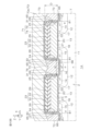
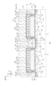
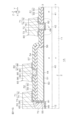
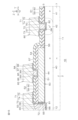
- FIG. 1 is a plan view showing a semiconductor device according to a first embodiment.
- FIG. 2 is a cross-sectional view taken along the line II-II shown in FIG.
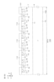
- FIG. 3 is a plan view showing an example of the layout of the first main surface.
- FIG. 4 is an enlarged plan view showing a main portion of the first main surface.
- FIG. 5 is an enlarged plan view showing further essential parts of the first main surface.
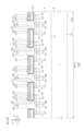
- FIG. 6 is a cross-sectional view taken along the line VI-VI shown in FIG.
- FIG. 7 is an enlarged cross-sectional view showing the main part of FIG. 6 together with the gate structure according to the first example.
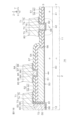
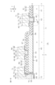
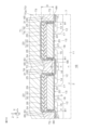
- FIG. 8 is a cross-sectional view taken along line VIII-VIII shown in FIG. FIG.
- FIG. 10A is an enlarged cross-sectional view showing a gate structure according to the second example.
- FIG. 10B is an enlarged cross-sectional view showing the gate structure according to the third example.
- FIG. 10C is an enlarged cross-sectional view showing a gate structure according to the fourth example.
- FIG. 10D is an enlarged cross-sectional view showing a gate structure according to the fifth example.
- FIG. 10E is an enlarged cross-sectional view showing a gate structure according to the sixth example.
- FIG. 10F is an enlarged cross-sectional view showing a gate structure according to the seventh example.
- FIG. 10A is an enlarged cross-sectional view showing a gate structure according to the second example.
- FIG. 10B is an enlarged cross-sectional view showing the gate structure according to the third example.
- FIG. 10C is an enlarged cross-sectional view showing a gate structure according to the fourth example.
- FIG. 10D is an enlarged cross-sectional view showing a gate structure according to the fifth
- FIG. 10G is an enlarged cross-sectional view showing a gate structure according to the eighth example.
- FIG. 10H is an enlarged cross-sectional view showing the gate structure according to the ninth example.
- FIG. 10I is an enlarged cross-sectional view showing a gate structure according to the tenth example.
- FIG. 10J is an enlarged cross-sectional view showing a gate structure according to the eleventh example.
- FIG. 11A is an enlarged cross-sectional view showing a wiring structure according to the second example.
- FIG. 11B is an enlarged cross-sectional view showing the wiring structure according to the third example.
- FIG. 11C is an enlarged cross-sectional view showing the wiring structure according to the fourth example.
- FIG. 11D is an enlarged cross-sectional view showing the wiring structure according to the fifth example.
- FIG. 11A is an enlarged cross-sectional view showing a wiring structure according to the second example.
- FIG. 11B is an enlarged cross-sectional view showing the wiring structure according to the third
- FIG. 11E is an enlarged cross-sectional view showing the wiring structure according to the sixth example.
- FIG. 11F is an enlarged cross-sectional view showing the wiring structure according to the seventh example.
- FIG. 11G is an enlarged cross-sectional view showing a wiring structure according to the eighth example.
- FIG. 11H is an enlarged cross-sectional view showing the wiring structure according to the ninth example.
- FIG. 11I is an enlarged cross-sectional view showing the wiring structure according to the tenth example.
- FIG. 12 is a schematic diagram showing a wafer used in the manufacture of semiconductor devices.
- FIG. 13A is a cross-sectional view showing a method for manufacturing a semiconductor device.
- FIG. 13B is a cross-sectional view showing a step subsequent to FIG. 13A.
- FIG. 13C is a cross-sectional view showing a step subsequent to FIG. 13B.
- FIG. 13D is a cross-sectional view showing a step subsequent to FIG. 13C.
- FIG. 13E is a cross-sectional view showing a step subsequent to FIG. 13D.
- FIG. 13F is a cross-sectional view showing a step subsequent to FIG. 13E.
- FIG. 13G is a cross-sectional view showing a step subsequent to FIG. 13F.
- FIG. 13H is a cross-sectional view showing a step subsequent to FIG. 13G.
- FIG. 13I is a cross-sectional view showing a step subsequent to FIG. 13H.
- FIG. 13J is a cross-sectional view showing a step subsequent to FIG. 13I.
- FIG. 13K is a cross-sectional view showing a step subsequent to FIG. 13J.
- FIG. 13L is a cross-sectional view showing a step subsequent to FIG. 13K.
- FIG. 13M is a cross-sectional view showing a step subsequent to FIG. 13L.
- FIG. 13N is a cross-sectional view showing a step subsequent to FIG. 13M.
- FIG. 13O is a cross-sectional view showing a step subsequent to FIG. 13N.
- FIG. 13P is a cross-sectional view showing a step subsequent to that shown in FIG. 13O.
- FIG. 13Q is a cross-sectional view showing a step subsequent to FIG. 13P.
- FIG. 13R is a cross-sectional view showing a step subsequent to FIG. 13Q.
- FIG. 14 is an enlarged cross-sectional view showing a gate structure of a semiconductor device according to the second embodiment.
- FIG. 15 is an enlarged cross-sectional view showing the wiring structure of the semiconductor device shown in FIG. 16A is a cross-sectional view showing a manufacturing method of the semiconductor device shown in FIG.
- FIG. 16B is a cross-sectional view showing a step subsequent to that of FIG. 16A.
- FIG. 16C is a cross-sectional view showing a step subsequent to FIG. 16B.
- FIG. 17 is a cross-sectional view showing a semiconductor device according to the third embodiment.
- FIG. 18 is a cross-sectional view showing a first modified example of the main source electrode.
- FIG. 19 is a cross-sectional view showing a second modified example of the source main electrode.
- this term includes a numerical value (shape) that is equal to the numerical value (shape) of the comparison target, as well as a numerical error (shape error) within a range of ⁇ 10% based on the numerical value (shape) of the comparison target.
- shape a numerical value that is equal to the numerical value (shape) of the comparison target
- error a numerical error within a range of ⁇ 10% based on the numerical value (shape) of the comparison target.
- the conductivity type of a semiconductor is indicated using “p-type” or “n-type”, but “p-type” may also be referred to as the “first conductivity type” and “n-type” as the “second conductivity type”. Of course, “n-type” may also be referred to as the "first conductivity type” and “p-type” as the “second conductivity type”.
- P-type is a conductivity type resulting from a trivalent element
- n-type is a conductivity type resulting from a pentavalent element.
- the trivalent element is at least one of boron, aluminum, gallium, and indium.
- the pentavalent element is at least one of nitrogen, phosphorus, arsenic, antimony, and bismuth.
- FIG. 1 is a plan view showing a semiconductor device 1A according to a first embodiment.
- FIG. 2 is a cross-sectional view taken along line II-II shown in FIG. 1.
- FIG. 3 is a plan view showing an example layout of the first main surface 3.
- FIG. 4 is an enlarged plan view showing a main portion of the first main surface 3.
- FIG. 5 is an enlarged plan view showing further main portions of the first main surface 3.
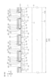
- FIG. 6 is a cross-sectional view taken along line VI-VI shown in FIG. 5.
- FIG. 7 is an enlarged cross-sectional view showing the main part of FIG. 6 together with the gate structure 20 according to the first example.
- FIG. 8 is a cross-sectional view taken along line VIII-VIII shown in FIG. 5.
- FIG. 9 is an enlarged cross-sectional view showing the main part of FIG. 8 together with the wiring structure 50 according to the first example.
- semiconductor device 1A is a semiconductor switching device having an insulated gate type transistor structure Tr as an example of a device structure.
- the transistor structure Tr has a vertical type structure.
- Semiconductor device 1A is a SiC semiconductor device having a chip 2 including a SiC single crystal. Chip 2 may be referred to as a "SiC chip” or a "semiconductor chip”.
- the chip 2 is made of hexagonal SiC single crystal and is formed into a rectangular parallelepiped shape.
- the hexagonal SiC single crystal has a number of polytypes including 2H (Hexagonal)-SiC single crystal, 4H-SiC single crystal, 6H-SiC single crystal, etc.
- the chip 2 is made of 4H-SiC single crystal, but the chip 2 may be made of other polytypes.
- the chip 2 has a first main surface 3 on one side, a second main surface 4 on the other side, and first to fourth side surfaces 5A to 5D connecting the first main surface 3 and the second main surface 4.
- the first main surface 3 and the second main surface 4 are formed in a quadrangular shape in a plan view seen from the vertical direction Z (hereinafter simply referred to as "plan view").
- the vertical direction Z is also the thickness direction of the chip 2 and the normal direction of the first main surface 3 (second main surface 4).
- the first main surface 3 and the second main surface 4 may be formed in a square or rectangular shape in a plan view.
- the first main surface 3 and the second main surface 4 are preferably formed by the c-plane of the SiC single crystal.
- the first main surface 3 is formed by the silicon surface ((0001) surface) of the SiC single crystal
- the second main surface 4 is formed by the carbon surface ((000-1) surface) of the SiC single crystal.
- the first side surface 5A and the second side surface 5B extend in a first direction X along the first main surface 3 and face a second direction Y that intersects with the first direction X along the first main surface 3. Specifically, the second direction Y is perpendicular to the first direction X.
- the third side surface 5C and the fourth side surface 5D extend in the second direction Y and face the first direction X.
- the first direction X is the m-axis direction ([1-100] direction) of the SiC single crystal
- the second direction Y is the a-axis direction ([11-20] direction) of the SiC single crystal.
- the first direction X may be the a-axis direction of the SiC single crystal
- the second direction Y may be the m-axis direction of the SiC single crystal.
- the direction extending along the first main surface 3 may be referred to as the "horizontal direction.”
- the horizontal direction is also the XY plane (horizontal plane) formed by the first direction X and the second direction Y, and is perpendicular to the vertical direction Z.
- the chip 2 (first main surface 3 and second main surface 4) has an off angle that is inclined at a predetermined angle in a predetermined off direction with respect to the c-plane of the SiC single crystal.
- the c-axis ((0001) axis) of the SiC single crystal is inclined from the vertical axis toward the off direction by the off angle.
- the c-plane of the SiC single crystal is inclined by the off angle with respect to the horizontal plane.
- the off-direction is preferably the a-axis direction of the SiC single crystal (i.e., the second direction Y).
- the off-angle may be greater than 0° and less than or equal to 10°.
- the off-angle may have a value that falls within at least one of the following ranges: greater than 0° and less than or equal to 1°, 1° or more and less than or equal to 2.5°, 2.5° or more and less than or equal to 5°, 5° or more and less than or equal to 7.5°, and 7.5° or more and less than or equal to 10°.
- the off angle is preferably 5° or less. It is particularly preferable that the off angle be 2° or more and 4.5° or less.
- the off angle is typically set in the range of 4° ⁇ 0.1°. This specification does not exclude a configuration in which the off angle is 0° (i.e., a configuration in which the first main surface 3 is a just plane relative to the c-plane).
- the chip 2 has a layered structure including a first semiconductor layer 6 and a second semiconductor layer 7.
- the first semiconductor layer 6 is made of a substrate (SiC substrate) including a SiC single crystal (semiconductor single crystal) and has the off direction and off angle described above.
- the first semiconductor layer 6 forms the second main surface 4 and forms part of the first to fourth side surfaces 5A to 5D.
- the first semiconductor layer 6 may have a thickness of 10 ⁇ m or more and 500 ⁇ m or less.
- the thickness of the first semiconductor layer 6 may have a value that belongs to at least one of the following ranges: 10 ⁇ m or more and 50 ⁇ m or less, 50 ⁇ m or more and 100 ⁇ m or less, 100 ⁇ m or more and 150 ⁇ m or less, 150 ⁇ m or more and 200 ⁇ m or less, 200 ⁇ m or more and 300 ⁇ m or less, 300 ⁇ m or more and 400 ⁇ m or less, and 400 ⁇ m or more and 500 ⁇ m or less.
- the second semiconductor layer 7 is made of an epitaxial layer (SiC epitaxial layer) containing a SiC single crystal (semiconductor single crystal) and is laminated on the first semiconductor layer 6.
- the second semiconductor layer 7 has the off direction and off angle described above.
- the second semiconductor layer 7 forms the first main surface 3 and forms part of the first to fourth side surfaces 5A to 5D. It is preferable that the second semiconductor layer 7 has a thickness less than the thickness of the first semiconductor layer 6. The thickness of the second semiconductor layer 7 may be greater than the thickness of the first semiconductor layer 6.
- the thickness of the second semiconductor layer 7 may be 5 ⁇ m or more and 50 ⁇ m or less.
- the thickness of the second semiconductor layer 7 may have a value that belongs to at least one of the following ranges: 5 ⁇ m or more and 10 ⁇ m or less, 10 ⁇ m or more and 15 ⁇ m or less, 15 ⁇ m or more and 20 ⁇ m or less, 20 ⁇ m or more and 25 ⁇ m or less, 25 ⁇ m or more and 30 ⁇ m or less, 30 ⁇ m or more and 35 ⁇ m or less, 35 ⁇ m or more and 40 ⁇ m or less, 40 ⁇ m or more and 45 ⁇ m, and 45 ⁇ m or more and 50 ⁇ m or less.
- the semiconductor device 1A includes an active region 8 set in the inner part of the chip 2 (first main surface 3).
- the active region 8 includes a transistor structure Tr (device structure) and is a region where an output current (drain current) is generated.
- the active region 8 is set in the inner part of the chip 2 at a distance from the periphery of the chip 2 (first to fourth side faces 5A to 5D) in a plan view.
- the active region 8 is set in a polygonal shape (a square shape in this embodiment) having four sides parallel to the periphery of the chip 2 in a plan view.
- the planar area of the active region 8 is preferably 50% to 90% of the planar area of the first main surface 3.
- the semiconductor device 1A includes a peripheral region 9 that is set outside the active region 8 in the chip 2.
- the peripheral region 9 is a region that does not include a device structure (transistor structure Tr).
- the peripheral region 9 is set on the periphery of the chip 2 (first main surface 3). In other words, the peripheral region 9 is provided in the region between the periphery of the chip 2 and the active region 8 in a planar view.
- the peripheral region 9 extends in a band shape along the active region 8 in a planar view, and is set in a polygonal ring shape (a square ring in this embodiment) that surrounds the active region 8.
- the semiconductor device 1A includes an n-type first semiconductor region 10 formed in the surface layer of the second main surface 4 in the active region 8.
- a drain potential is applied to the first semiconductor region 10 as a first potential (high potential).
- the first semiconductor region 10 may be referred to as a "drain region", a "first region”, etc.
- the first semiconductor region 10 extends in a layer shape along the second main surface 4.
- the first semiconductor region 10 is formed over the entire active region 8.
- the first semiconductor region 10 is extended from the active region 8 to the peripheral region 9, and has a portion located in the surface layer of the second main surface 4 in the peripheral region 9.
- the first semiconductor region 10 is extended from the active region 8 to the peripheral region 9 over the entire periphery.
- the first semiconductor region 10 is exposed from at least one of the first to fourth side surfaces 5A to 5D. In this embodiment, the first semiconductor region 10 is exposed from the entire periphery of the first to fourth side surfaces 5A to 5D.
- the first semiconductor region 10 is formed in the first semiconductor layer 6.
- the first semiconductor region 10 is formed in the entire thickness range between the lower end (second main surface 4) of the first semiconductor layer 6 and the upper end (second semiconductor layer 7) of the first semiconductor layer 6, and is connected to the second semiconductor layer 7.
- the first semiconductor region 10 is formed using the n-type first semiconductor layer 6, and has a thickness corresponding to the thickness of the first semiconductor layer 6.
- the first semiconductor region 10 may be formed by introducing n-type impurities into the surface layer portion of the second main surface 4.
- the semiconductor device 1A includes an n-type second semiconductor region 11 formed in the surface layer of the first main surface 3 in the active region 8.
- the second semiconductor region 11 may be referred to as a "drift region", a “second region”, etc.
- the second semiconductor region 11 has an impurity concentration lower than the impurity concentration of the first semiconductor region 10.
- the second semiconductor region 11 extends in a layer shape along the first main surface 3 and is electrically connected to the first semiconductor region 10 inside the chip 2.
- the second semiconductor region 11 is formed over the entire active region 8.
- the second semiconductor region 11 is extended from the active region 8 to the peripheral region 9, and has a portion in the peripheral region 9 that is located in the surface layer of the first main surface 3.
- the second semiconductor region 11 is pulled out from the active region 8 to the peripheral region 9 along the entire periphery. It is preferable that the second semiconductor region 11 is exposed from at least one of the first to fourth side faces 5A to 5D. In this embodiment, the second semiconductor region 11 is exposed from the entire periphery of the first to fourth side faces 5A to 5D.
- the second semiconductor region 11 is formed in the second semiconductor layer 7.
- the second semiconductor region 11 is formed throughout the thickness range between the upper end (first semiconductor region 10) of the first semiconductor layer 6 and the upper end (first main surface 3) of the second semiconductor layer 7, and is connected to the first semiconductor layer 6 (first semiconductor region 10).
- the second semiconductor region 11 is formed using the n-type second semiconductor layer 7, and has a thickness corresponding to the thickness of the second semiconductor layer 7.
- the second semiconductor region 11 may be formed by introducing n-type impurities into the surface layer of the first main surface 3.
- the semiconductor device 1A includes a plurality of p-type body regions 12 formed at intervals in the surface layer portion of the first main surface 3 in the active region 8.
- the plurality of body regions 12 are each formed in the surface layer portion of the second semiconductor region 11.
- the plurality of body regions 12 have a p-type impurity concentration higher than the n-type impurity concentration of the second semiconductor region 11.
- a source potential is applied to the body regions 12 as a second potential (low potential) different from the first potential (high potential).
- the multiple body regions 12 are arranged at intervals in the first direction X, and are each formed in a band shape extending in the second direction Y. In other words, the multiple body regions 12 are arranged in stripes extending in the second direction Y. Furthermore, the extension direction of the multiple body regions 12 coincides with the off-direction of the SiC single crystal.
- the multiple body regions 12 are formed at intervals from the bottom of the second semiconductor region 11 toward the first major surface 3, and face the first semiconductor region 10 across a portion of the second semiconductor region 11. It is preferable that the multiple body regions 12 are formed at intervals from the middle of the second semiconductor region 11 toward the first major surface 3.
- the multiple body regions 12 may cross the depth position of the middle part of the second semiconductor region 11 in the thickness direction.
- the multiple body regions 12 are exposed from the first main surface 3.
- the multiple body regions 12 each form a pn junction (pn junction diode: body diode) with the second semiconductor region 11, and expand a depletion layer into the second semiconductor region 11 when a reverse bias voltage is applied.
- the body regions 12 may each have a width of 1 ⁇ m or more and 10 ⁇ m or less.
- the width of the body regions 12 may have a value that belongs to at least one of the following ranges: 1 ⁇ m or more and 2 ⁇ m or less, 2 ⁇ m or more and 3 ⁇ m or less, 3 ⁇ m or more and 4 ⁇ m or less, 4 ⁇ m or more and 5 ⁇ m or less, 5 ⁇ m or more and 6 ⁇ m or less, 6 ⁇ m or more and 7 ⁇ m or less, 7 ⁇ m or more and 8 ⁇ m or less, 8 ⁇ m or more and 9 ⁇ m or less, and 9 ⁇ m or more and 10 ⁇ m or less.
- the width of the body regions 12 is preferably 1.5 ⁇ m or more and 2.5 ⁇ m or less.
- the body regions 12 may each have a thickness (depth) of 0.1 ⁇ m or more and 2.5 ⁇ m or less.
- the thickness of the body regions 12 may have a value that belongs to at least one of the following ranges: 0.1 ⁇ m or more and 0.5 ⁇ m or less, 0.5 ⁇ m or more and 1 ⁇ m or less, 1 ⁇ m or more and 1.5 ⁇ m or less, 1.5 ⁇ m or more and 2 ⁇ m or less, and 2 ⁇ m or more and 2.5 ⁇ m or less.
- the thickness of the body regions 12 is preferably 0.5 ⁇ m or more and 1.5 ⁇ m or less.
- the semiconductor device 1A includes a plurality of n-type surface drift regions 13 formed in a surface portion of the first main surface 3.
- each of the plurality of surface drift regions 13 is made of a portion of the second semiconductor region 11.
- the plurality of surface drift regions 13 may have an n-type impurity concentration higher than the n-type impurity concentration of the second semiconductor region 11, or may have an n-type impurity concentration lower than the n-type impurity concentration of the second semiconductor region 11.
- the multiple surface drift regions 13 are each partitioned into regions between multiple body regions 12 adjacent in the first direction X in the surface portion of the second semiconductor region 11.
- the multiple surface drift regions 13 are arranged at intervals in the first direction X and are each formed in a band shape extending in the second direction Y.
- the multiple surface drift regions 13 are also formed in a stripe shape extending in the second direction Y.
- the surface drift region 13 forms a pnp-type JFET structure with the multiple body regions 12 located on both sides.
- the width of the surface drift region 13 is preferably less than the width of the body region 12.
- the width of the surface drift region 13 may be greater than the width of the body region 12.
- the surface drift region 13 has a width in the horizontal direction (first direction X in this embodiment) of 0.1 ⁇ m or more and 5 ⁇ m or less.
- the width of the surface drift region 13 may have a value that falls within at least one of the following ranges: 0.1 ⁇ m to 0.5 ⁇ m, 0.5 ⁇ m to 1 ⁇ m, 1 ⁇ m to 1.5 ⁇ m, 1.5 ⁇ m to 2 ⁇ m, 2 ⁇ m to 2.5 ⁇ m, 2.5 ⁇ m to 3 ⁇ m, 3 ⁇ m to 3.5 ⁇ m, 3.5 ⁇ m to 4 ⁇ m, 4 ⁇ m to 4.5 ⁇ m, and 4.5 ⁇ m to 5 ⁇ m.
- the width of the surface drift region 13 is preferably 0.5 ⁇ m to 2 ⁇ m.
- the semiconductor device 1A includes a plurality of n-type source regions 14, 15 formed in the surface layer of each of the body regions 12.
- the source regions 14, 15 have an n-type impurity concentration higher than the n-type impurity concentration of the second semiconductor region 11.
- a source potential is applied to the source regions 14, 15.
- the multiple source regions 14, 15 include a first source region 14 located on one side (third side surface 5C side) in the first direction X in the surface layer portion of each body region 12, and a second source region 15 located on the other side (fourth side surface 5D side) in the first direction X.
- one first source region 14 is formed on one end side of the body region 12
- one second source region 15 is formed on the other end side of the body region 12.
- the first source region 14 is formed at a distance from one end to the other end of the body region 12.
- the second source region 15 is formed at a distance from the first source region 14 to the other end of the body region 12.
- the second source region 15 is formed at a distance from the other end to one end of the body region 12.
- the multiple source regions 14, 15 extend in a band shape along the extension direction of the body region 12.
- the multiple source regions 14, 15 are formed spaced apart inward from both ends of the body region 12 in the second direction Y, and both ends of the body region 12 are exposed from the first main surface 3 (see FIG. 5).
- the multiple source regions 14, 15 are formed at intervals from the bottom of the body region 12 toward the first main surface 3, and face the second semiconductor region 11 across a portion of the body region 12. It is preferable that the multiple source regions 14, 15 are formed at intervals from the middle of the body region 12 toward the first main surface 3.
- each first source region 14 may be formed at intervals in the extension direction of the body region 12. In this case, each first source region 14 may be formed in a strip extending in the second direction Y.
- the multiple second source regions 15 may be formed at intervals in the extension direction of the body region 12. In this case, each second source region 15 may be formed in a strip extending in the second direction Y.
- the semiconductor device 1A includes a plurality of p-type contact regions 16 formed in a surface portion of the body region 12 in a region different from the plurality of source regions 14, 15.
- the contact region 16 may be referred to as a "backgate region.”
- the plurality of contact regions 16 have a p-type impurity concentration higher than the p-type impurity concentration of the body region 12.
- a source potential is applied to the plurality of contact regions 16.
- one contact region 16 is interposed in the region between the first source region 14 and the second source region 15 in the surface layer portion of one body region 12, and is electrically connected to the body region 12.
- the contact region 16 extends in a band shape along the extension direction of the body region 12 (source regions 14, 15).
- the contact region 16 is formed spaced inward from both ends of the body region 12 in the second direction Y, exposing both ends of the body region 12 from the first main surface 3 (see FIG. 5).
- the contact region 16 has a width smaller than the width of the source regions 14, 15.
- the width of the contact region 16 may be larger than the width of the source regions 14, 15.
- the contact region 16 is formed at a distance from the bottom of the body region 12 toward the first main surface 3, and faces the second semiconductor region 11 across a portion of the body region 12.
- the contact region 16 is preferably formed at a distance from the middle of the body region 12 toward the first main surface 3.
- the contact region 16 has a thickness (depth) greater than the thickness (depth) of the source regions 14, 15, and has a bottom located closer to the bottom of the body region 12 than the bottoms of the source regions 14, 15.
- each contact region 16 may be formed at intervals in the extension direction of the body region 12.
- each contact region 16 may be formed in a strip shape extending in the second direction Y.
- the semiconductor device 1A includes a plurality of p-type channel regions 17, 18 formed in a surface layer portion of the first main surface 3.
- the plurality of channel regions 17, 18 are respectively formed in surface layers of the plurality of body regions 12.
- the plurality of channel regions 17, 18 include a first channel region 17 on one side in the first direction X and a second channel region 18 on the other side in the first direction X.
- the first channel region 17 is formed in a region between the second semiconductor region 11 (surface drift region 13) and the first source region 14 in the surface portion of the body region 12.
- the second channel region 18 is formed in a region between the second semiconductor region 11 (surface drift region 13) and the second source region 15 in the surface portion of the body region 12.
- the multiple channel regions 17, 18 are arranged at intervals in the first direction X and are each formed in a band shape extending in the second direction Y. In other words, the multiple channel regions 17, 18 are arranged in stripes extending in the second direction Y.
- the semiconductor device 1A includes a plurality of planar electrode type gate structures 20 arranged on the first main surface 3 in the active region 8.
- the plurality of gate structures 20 constitute the gates of a vertical transistor structure Tr.
- the multiple gate structures 20 are arranged at intervals in the first direction X, and are each formed in a band shape extending in the second direction Y. In other words, the multiple gate structures 20 are arranged in stripes extending in the second direction Y. Furthermore, the extension direction of the multiple gate structures 20 coincides with the off-direction of the SiC single crystal.
- the multiple gate structures 20 each include a gate insulating film 21, a gate electrode 22, a first planar insulating film 23, and multiple sidewall insulating films 24, 25.
- the configuration of one gate structure 20 is described below.
- the gate insulating film 21 may include at least one of a silicon oxide film, a silicon nitride film, and a silicon oxynitride film.
- the gate insulating film 21 has a single-layer structure made of a silicon oxide film. It is preferable that the gate insulating film 21 includes a silicon oxide film made of an oxide of the chip 2.
- the gate insulating film 21 covers the first main surface 3 in a film-like shape.
- the gate insulating film 21 extends in a band shape in the second direction Y in a plan view.
- the gate insulating film 21 covers at least one of the channel regions 17, 18.
- the gate insulating film 21 crosses one surface drift region 13 and spans two adjacent body regions 12, covering the surface drift region 13 and the multiple channel regions 17, 18.
- the gate insulating film 21 spans the first source region 14 on one body region 12 side and the second source region 15 on the other body region 12 side, and covers the surface drift region 13, the first source region 14, the second source region 15, the first channel region 17, and the second channel region 18.
- the gate insulating film 21 partially covers the first source region 14 at a distance from the contact region 16, and exposes a part of the first source region 14 and the contact region 16 from the first main surface 3.
- the gate insulating film 21 partially covers the second source region 15 at a distance from the contact region 16, and exposes a part of the second source region 15 and the contact region 16 from the first main surface 3.
- the gate insulating film 21 may have a thickness of 10 nm or more and 150 nm or less.
- the thickness of the gate insulating film 21 may have a value that belongs to at least one of the following ranges: 10 nm or more and 25 nm or less, 25 nm or more and 50 nm or less, 50 nm or more and 75 nm or less, 75 nm or more and 100 nm or less, 100 nm or more and 125 nm or less, and 125 nm or more and 150 nm or less.
- the thickness of the gate insulating film 21 is preferably 25 nm or more and 75 nm or less.
- the gate electrode 22 is disposed on the gate insulating film 21.
- a gate potential is applied to the gate electrode 22 as a control potential.
- the gate electrode 22 may include either or both of p-type conductive polysilicon and n-type conductive polysilicon.
- the conductivity type of the gate electrode 22 is adjusted according to the gate threshold voltage to be achieved.
- the gate electrode 22 extends in a strip shape in the second direction Y in a plan view.
- the gate electrode 22 is formed spaced inward from both ends of the gate insulating film 21 in the first direction X, exposing both ends of the gate insulating film 21.
- the gate electrode 22 exposes the multiple source regions 14, 15 and the multiple contact regions 16.
- the gate electrode 22 is disposed on the gate insulating film 21 so as to face at least one of the channel regions 17, 18.
- the gate electrode 22 crosses one surface drift region 13 and spans two adjacent body regions 12, and faces the surface drift region 13 and the multiple channel regions 17, 18 across the gate insulating film 21.
- the gate electrode 22 spans the first source region 14 on one body region 12 side and the second source region 15 on the other body region 12 side, and faces the surface drift region 13, the first source region 14, the second source region 15, the first channel region 17, and the second channel region 18 across the gate insulating film 21.
- the gate electrode 22 has an electrode surface 26, a first sidewall 27 on one side in the first direction X, and a second sidewall 28 on the other side in the first direction X.
- the electrode surface 26 extends flat along the gate insulating film 21 (first main surface 3).
- the electrode surface 26 may extend approximately parallel to the gate insulating film 21 (first main surface 3).
- the first sidewall 27 is formed at a distance from one end of the gate insulating film 21 to the other end in the first direction X, and extends in the vertical direction Z.
- the second sidewall 28 is formed at a distance from the other end of the gate insulating film 21 to the one end in the first direction X, and extends in the vertical direction Z.
- the first sidewall 27 and the second sidewall 28 may extend substantially perpendicular to the gate insulating film 21. That is, the gate electrode 22 may be formed in a quadrangular shape (flattened rectangular shape) in cross-sectional view. The first sidewall 27 and the second sidewall 28 may be inclined obliquely toward the electrode surface 26. That is, the gate electrode 22 may be formed in a tapered shape (preferably an isosceles trapezoidal shape) in cross-sectional view.
- the gate electrode 22 may have a width of 1 ⁇ m or more and 10 ⁇ m or less.
- the width of the gate electrode 22 is the width in a direction perpendicular to the extension direction (i.e., the first direction X).
- the width of the gate electrode 22 may have a value belonging to at least one of the ranges of 1 ⁇ m or more and 2.5 ⁇ m or less, 2.5 ⁇ m or more and 5 ⁇ m or less, 5 ⁇ m or more and 7.5 ⁇ m or less, and 7.5 ⁇ m or more and 10 ⁇ m or less.
- the width of the gate electrode 22 is preferably 1.5 ⁇ m or more and 2.5 ⁇ m or less.
- the gate electrode 22 may have a thickness of 0.1 ⁇ m or more and 2 ⁇ m or less.
- the thickness of the gate electrode 22 may have a value that belongs to at least one of the following ranges: 0.1 ⁇ m or more and 0.5 ⁇ m or less, 0.5 ⁇ m or more and 1 ⁇ m or less, 1 ⁇ m or more and 1.5 ⁇ m or less, and 1.5 ⁇ m or more and 2 ⁇ m or less.
- the thickness of the gate electrode 22 is preferably 0.2 ⁇ m or more and 1 ⁇ m or less.
- the first planar insulating film 23 is disposed on the gate electrode 22. Specifically, the first planar insulating film 23 covers the electrode surface 26 in a film-like manner, and exposes both the first sidewall 27 and the second sidewall 28. The first planar insulating film 23 does not have a portion that covers the gate insulating film 21. The first planar insulating film 23 extends in a band shape in the second direction Y in a plan view.
- the first planar insulating film 23 has a first insulating surface 29, a first insulating sidewall 30 on one side in the first direction X, and a second insulating sidewall 31 on the other side in the first direction X.
- the first insulating surface 29 extends flat along the electrode surface 26.
- the first insulating surface 29 may extend approximately parallel to the electrode surface 26.
- the first insulating sidewall 30 extends in the vertical direction Z above the gate electrode 22 and is connected to the first sidewall 27 of the gate electrode 22.
- the first insulating sidewall 30 may be formed flush with the first sidewall 27.
- the first insulating sidewall 30 may be located outward from the first sidewall 27 and face the gate insulating film 21 in the stacking direction.
- the first insulating sidewall 30 may be located on the electrode surface 26 at a distance from the first sidewall 27 and expose the peripheral portion of the electrode surface 26. In this case, the first insulating sidewall 30 may be connected to the first sidewall 27 via the peripheral portion of the electrode surface 26.
- the second insulating sidewall 31 extends in the vertical direction Z above the gate electrode 22 and is connected to the second sidewall 28 of the gate electrode 22.
- the second insulating sidewall 31 may be formed flush with the second sidewall 28.
- the second insulating sidewall 31 may be located outward of the second sidewall 28 and face the gate insulating film 21 in the stacking direction.
- the second insulating sidewall 31 may be located on the electrode surface 26 at a distance from the second sidewall 28 and expose the peripheral portion of the electrode surface 26. In this case, the second insulating sidewall 31 may be connected to the second sidewall 28 via the peripheral portion of the electrode surface 26.
- the first insulating sidewall 30 and the second insulating sidewall 31 may extend substantially perpendicular to the gate insulating film 21. That is, the first planar insulating film 23 may be formed in a quadrangular shape (flattened rectangular shape) in cross-sectional view. The first insulating sidewall 30 and the second insulating sidewall 31 may be inclined obliquely toward the first insulating surface 29. That is, the first planar insulating film 23 may be formed in a tapered shape (preferably an isosceles trapezoidal shape) in cross-sectional view.
- the first planar insulating film 23 may have a thickness of 0.1 ⁇ m or more and 2 ⁇ m or less.
- the thickness of the first planar insulating film 23 may have a value that belongs to at least one of the following ranges: 0.1 ⁇ m or more and 0.5 ⁇ m or less, 0.5 ⁇ m or more and 1 ⁇ m or less, 1 ⁇ m or more and 1.5 ⁇ m or less, and 1.5 ⁇ m or more and 2 ⁇ m or less.
- the thickness of the first planar insulating film 23 is preferably 0.2 ⁇ m or more.
- the first planar insulating film 23 may include at least one of a silicon oxide film, a silicon nitride film, and a silicon oxynitride film.
- the first planar insulating film 23 may have a single-layer structure consisting of a single insulating film.
- the first planar insulating film 23 may have a layered structure including a plurality of insulating films.
- the first planar insulating film 23 has a layered structure including a first oxide film 32 (first insulating film) and a second oxide film 33 (second insulating film) that are layered in this order from the gate electrode 22 side.
- the first oxide film 32 has a single-layer structure made of a silicon oxide film with no added impurities.
- the silicon oxide film with no added impurities may be called an NSG film (nondoped silicate glass film).
- the first oxide film 32 directly covers the electrode surface 26 in a film-like manner, exposing both the first side wall 27 and the second side wall 28.
- the first oxide film 32 extends in a band-like manner in the second direction Y in a plan view, and forms part of the first insulating side wall 30 and part of the second insulating side wall 31.
- the first oxide film 32 may have a thickness of 0.01 ⁇ m or more and 0.2 ⁇ m or less.
- the thickness of the first oxide film 32 may have a value that belongs to at least one of the following ranges: 0.01 ⁇ m or more and 0.05 ⁇ m or less, 0.05 ⁇ m or more and 0.1 ⁇ m or less, 0.1 ⁇ m or more and 0.15 ⁇ m or less, and 0.15 ⁇ m or more and 0.2 ⁇ m or less.
- the thickness of the first oxide film 32 is preferably 0.05 ⁇ m or more.
- the second oxide film 33 may have a single layer structure made of a silicon oxide film containing phosphorus, or a multilayer structure including a silicon oxide film containing phosphorus.
- the silicon oxide film containing phosphorus may contain boron.
- the silicon oxide film containing phosphorus may be called a PSG film (Phosphorus Silicon Glass film).
- the silicon oxide film containing both phosphorus and boron may be called a BPSG film (Boron Phosphorus Silicon Glass film).
- the second oxide film 33 may have a single layer structure made of a PSG film or a BPSG film stacked on the first oxide film 32.
- the second oxide film 33 may have a layered structure including a PSG film stacked on the first oxide film 32 and a BPSG film stacked on the PSG film.
- the second oxide film 33 may have a layered structure including a BPSG film stacked on the first oxide film 32 and a PSG film stacked on the BPSG film.
- the second oxide film 33 has a single layer structure made of a PSG film, as an example.
- the second oxide film 33 directly covers the first oxide film 32 in a film-like manner, exposing both the first side wall 27 and the second side wall 28.
- the second oxide film 33 extends in a band shape in the second direction Y in a plan view, and forms the first insulating surface 29, a part of the first insulating side wall 30, and a part of the second insulating side wall 31.
- the second oxide film 33 preferably has a thickness greater than that of the first oxide film 32.
- the thickness of the second oxide film 33 may be less than that of the first oxide film 32.
- the thickness of the second oxide film 33 may be 0.05 ⁇ m or more and 1.8 ⁇ m or less.
- the thickness of the second oxide film 33 may have a value that falls within at least one of the following ranges: 0.05 ⁇ m to 0.1 ⁇ m, 0.1 ⁇ m to 0.5 ⁇ m, 0.5 ⁇ m to 1 ⁇ m, 1 ⁇ m to 1.5 ⁇ m, and 1.5 ⁇ m to 1.8 ⁇ m.
- the thickness of the second oxide film 33 is preferably 0.1 ⁇ m or more.
- the second oxide film 33 improves the flatness of the first planar insulating film 23 (i.e., the film formability of the first planar insulating film 23 on the electrode surface 26). Fluctuations in the electrical characteristics of the gate electrode 22 caused by impurity diffusion in the second oxide film 33 are suppressed by the first oxide film 32, which contains no impurities. Fluctuations in the insulating characteristics of the second oxide film 33 caused by impurity diffusion in the gate electrode 22 are suppressed by the first oxide film 32, which contains no impurities.
- the multiple sidewall insulating films 24, 25 cover the first sidewall 27 and the second sidewall 28, respectively.
- the multiple sidewall insulating films 24, 25 include a first sidewall insulating film 24 that covers the first sidewall 27, and a second sidewall insulating film 25 that covers the second sidewall 28.
- the first sidewall insulating film 24 covers the first sidewall 27 on the gate insulating film 21.
- the first sidewall insulating film 24 is formed on the gate insulating film 21 at a distance from the contact region 16, and exposes a part of the second source region 15 and the contact region 16.
- the first sidewall insulating film 24 is disposed only on the gate insulating film 21, and does not have a portion that directly covers the second source region 15 or a portion that directly covers the contact region 16.
- the first sidewall insulating film 24 faces a part of the second source region 15 across the gate insulating film 21.
- the first sidewall insulating film 24 is formed at a distance from the second channel region 18 toward the inside of the body region 12.
- the first sidewall insulating film 24 does not have a part facing the second channel region 18 across the gate insulating film 21.
- the first sidewall insulating film 24 is extended from the first sidewall 27 toward the first insulating sidewall 30 of the first planar insulating film 23, and covers the first insulating sidewall 30.
- the first sidewall insulating film 24 has a portion that covers the first sidewall 27 and a portion that covers the first insulating sidewall 30.
- the first sidewall insulating film 24 also has a portion that covers the boundary between the gate electrode 22 and the first planar insulating film 23.
- the first sidewall insulating film 24 covers the first sidewall 27 and the first insulating sidewall 30 in a film shape following the inclination angle of the first sidewall 27 and the inclination angle of the first insulating sidewall 30.
- the first sidewall insulating film 24 extends at an inclination angle approximately equal to the inclination angle of the first sidewall 27 in the covering portion relative to the first sidewall 27, and has a film surface extending approximately parallel to the first sidewall 27.
- the first sidewall insulating film 24 extends at an inclination angle approximately equal to the inclination angle of the first insulating sidewall 30 in the covering portion relative to the first insulating sidewall 30, and has a film surface extending approximately parallel to the first insulating sidewall 30.
- the first sidewall insulating film 24 extends almost vertically in the region between the gate insulating film 21 (first main surface 3) and the first insulating surface 29.
- the first sidewall insulating film 24 has a film surface that extends in the vertical direction Z in the covering portion relative to the first sidewall 27, and has a film surface that extends in the vertical direction Z in the covering portion relative to the first insulating sidewall 30.
- the first sidewall insulating film 24 covers both the first oxide film 32 and the second oxide film 33 on the first insulating sidewall 30 side. In other words, the first sidewall insulating film 24 has a portion that covers the boundary between the first oxide film 32 and the second oxide film 33.
- the first sidewall insulating film 24 is formed on the first main surface 3 side of the first insulating surface 29, and exposes the first insulating surface 29. In other words, the first sidewall insulating film 24 exposes the second oxide film 33 from the first insulating surface 29.
- the second sidewall insulating film 25 covers the second sidewall 28 on the gate insulating film 21.
- the second sidewall insulating film 25 is formed on the gate insulating film 21 at a distance from the contact region 16, exposing a part of the first source region 14 and the contact region 16.
- the second sidewall insulating film 25 is disposed only on the gate insulating film 21, and does not have a portion that directly covers the first source region 14 or a portion that directly covers the contact region 16.
- the second sidewall insulating film 25 faces a part of the first source region 14 across the gate insulating film 21.
- the second sidewall insulating film 25 is formed at a distance from the first channel region 17 toward the inside of the body region 12.
- the second sidewall insulating film 25 does not have a part facing the first channel region 17 across the gate insulating film 21.
- the second sidewall insulating film 25 is extended from the second sidewall 28 toward the second insulating sidewall 31 of the first planar insulating film 23, and covers the second insulating sidewall 31.
- the second sidewall insulating film 25 has a portion that covers the second sidewall 28 and a portion that covers the second insulating sidewall 31.
- the second sidewall insulating film 25 also has a portion that covers the boundary between the gate electrode 22 and the first planar insulating film 23.
- the second sidewall insulating film 25 covers the second sidewall 28 and the second insulating sidewall 31 in a film shape following the inclination angle of the second sidewall 28 and the inclination angle of the second insulating sidewall 31.
- the second sidewall insulating film 25 extends at an inclination angle approximately equal to the inclination angle of the second sidewall 28 in the covering portion relative to the second sidewall 28, and has a film surface extending approximately parallel to the second sidewall 28.
- the second sidewall insulating film 25 extends at an inclination angle approximately equal to the inclination angle of the second insulating sidewall 31 in the covering portion relative to the second insulating sidewall 31, and has a film surface extending approximately parallel to the second insulating sidewall 31.
- the second sidewall insulating film 25 extends almost vertically in the region between the gate insulating film 21 (first main surface 3) and the first insulating surface 29.
- the second sidewall insulating film 25 has a film surface that extends in the vertical direction Z in the covering portion relative to the second sidewall 28, and has a film surface that extends in the vertical direction Z in the covering portion relative to the second insulating sidewall 31.
- the second sidewall insulating film 25 covers both the first oxide film 32 and the second oxide film 33 on the second insulating sidewall 31 side.
- the second sidewall insulating film 25 has a portion that covers the boundary between the first oxide film 32 and the second oxide film 33.
- the second sidewall insulating film 25 has a portion that faces the first sidewall insulating film 24 across the first oxide film 32, and a portion that faces the first sidewall insulating film 24 across the second oxide film 33.
- the second sidewall insulating film 25 is formed on the first main surface 3 side relative to the first insulating surface 29, exposing the first insulating surface 29. In other words, the second sidewall insulating film 25 exposes the second oxide film 33 from the first insulating surface 29.
- the multiple sidewall insulating films 24, 25 may include at least one of a silicon oxide film, a silicon nitride film, and a silicon oxynitride film.
- the multiple sidewall insulating films 24, 25 may each have a single-layer structure made of a single insulating film.
- the multiple sidewall insulating films 24, 25 may each have a layered structure including multiple insulating films.
- the sidewall insulating films 24, 25 each have a single-layer structure made of a silicon oxide film with no added impurities.
- the sidewall insulating films 24, 25 each consist of an NSG film.
- the sidewall insulating films 24, 25 each consist of a tetraethyl orthosilicate film, which is an example of an NSG film.
- the tetraethyl orthosilicate film may also be referred to as a "TEOS film (Tetraethyl orthosilicate film)."
- the multiple sidewall insulating films 24, 25 are made of NSG films (TEOS films), the multiple sidewall insulating films 24, 25 suppress the fluctuation in the electrical characteristics of the gate electrode 22 caused by the impurity diffusion in the second oxide film 33. In addition, the multiple sidewall insulating films 24, 25 suppress the fluctuation in the insulating characteristics of the second oxide film 33 caused by the impurity diffusion in the gate electrode 22.
- NSG films TEOS films
- the multiple sidewall insulating films 24, 25 each have a thickness less than the thickness of the gate electrode 22.
- the thickness of the multiple sidewall insulating films 24, 25 is the horizontal thickness of the multiple sidewall insulating films 24, 25 based on the first sidewall 27 or the second sidewall 28 of the gate electrode 22.
- the thickness of the multiple sidewall insulating films 24, 25 is less than the thickness (total thickness) of the first planar insulating film 23.
- the thickness of the multiple sidewall insulating films 24, 25 is preferably less than the thickness of the second oxide film 33.
- the thickness of the multiple sidewall insulating films 24, 25 is preferably less than the thickness of the first oxide film 32.
- the thickness of the multiple sidewall insulating films 24, 25 is preferably greater than the thickness of the gate insulating film 21.
- the thickness of the multiple sidewall insulating films 24, 25 may be less than the thickness of the gate insulating film 21.
- the thickness of the sidewall insulating films 24, 25 may be 0.05 ⁇ m or more and 0.5 ⁇ m or less.
- the thickness of the sidewall insulating films 24, 25 may have a value that belongs to at least one of the following ranges: 0.05 ⁇ m or more and 0.1 ⁇ m or less, 0.1 ⁇ m or more and 0.15 ⁇ m or less, 0.15 ⁇ m or more and 0.2 ⁇ m or less, 0.2 ⁇ m or more and 0.25 ⁇ m or less, 0.25 ⁇ m or more and 0.3 ⁇ m or less, 0.3 ⁇ m or more and 0.35 ⁇ m or less, 0.35 ⁇ m or more and 0.4 ⁇ m or less, 0.4 ⁇ m or more and 0.45 ⁇ m or less, and 0.45 ⁇ m or more and 0.5 ⁇ m or less.
- the thickness of the sidewall insulating films 24, 25 is preferably 0.1 ⁇ m or more and 0.3 ⁇ m or less.
- the gate structure 20 controls the inversion and non-inversion of the channel regions 17, 18 in response to a gate potential applied to the gate electrode 22.
- a gate potential is applied to the gate electrode 22
- the channel regions 17, 18 are turned on, and a drain current flows between the second semiconductor region 11 and the source regions 14, 15 via the channel regions 17, 18 (body region 12).
- a planar gate type transistor structure Tr is formed in the inner part (active region 8) of the chip 2.
- the semiconductor device 1A includes a p-type outer body region 40 formed in the surface layer of the first main surface 3 in the peripheral region 9.
- the outer body region 40 is formed in the surface layer of the second semiconductor region 11.
- the outer body region 40 has a p-type impurity concentration that is higher than the n-type impurity concentration of the second semiconductor region 11.
- the outer body region 40 preferably has a p-type impurity concentration that is approximately equal to the p-type impurity concentration of the body region 12.
- the p-type impurity concentration of the outer body region 40 may be less than the p-type impurity concentration of the body region 12, or may be higher than the p-type impurity concentration of the body region 12.
- the outer body region 40 is formed at a distance from the periphery of the first main surface 3 (first to fourth side surfaces 5A to 5D) toward the active region 8, and extends in a band along the active region 8.
- the outer body region 40 has a portion that extends in a band in the first direction X and a portion that extends in a band in the second direction Y in a plan view, and divides the body regions 12 (active regions 8) from multiple directions.
- the outer body region 40 collectively surrounds the multiple body regions 12 (active regions 8) in a plan view and is partitioned into a polygonal ring (a square ring in this embodiment) having four sides parallel to the periphery of the first main surface 3.
- the outer body region 40 forms the boundary between the active region 8 and the peripheral region 9.
- the outer body region 40 may have an edge portion that connects the portion extending in the first direction X and the portion extending in the second direction Y in a circular arc shape (preferably a quadrant arc shape) in a plan view (see FIG. 4).
- the outer body region 40 is exposed from the first main surface 3.
- the outer body region 40 is formed at a distance from the bottom of the second semiconductor region 11 toward the first main surface 3, and faces the first semiconductor region 10 across a portion of the second semiconductor region 11.
- the outer body region 40 is preferably formed at a distance from the middle of the second semiconductor region 11 toward the first main surface 3.
- the outer body region 40 may cross the depth position of the middle of the second semiconductor region 11 in the thickness direction.
- the outer body region 40 has an inner edge on the active region 8 side and an outer edge on the peripheral side of the first main surface 3.
- the inner edge of the outer body region 40 is connected to the body regions 12 in a portion extending in the first direction X, and defines the body regions 12 and the surface drift regions 13 in the surface portion of the second semiconductor region 11.
- the outer body region 40 is electrically connected to the multiple body regions 12. As a result, a source potential is applied to the outer body region 40 via the multiple body regions 12.
- the outer body region 40 forms a pn junction with the second semiconductor region 11, and expands a depletion layer into the second semiconductor region 11 when a reverse bias voltage is applied.
- the outer body region 40 is connected to the multiple body regions 12 at intervals in the second direction Y from the source regions 14, 15. Therefore, the outer body region 40 does not have the source regions 14, 15 in the surface layer portion (see FIG. 5). Also, the outer body region 40 is connected to the multiple body regions 12 at intervals in the second direction Y from the contact region 16. Therefore, the outer body region 40 does not have the contact region 16 in the surface layer portion (see FIG. 5).
- the outer body region 40 preferably has a width greater than the width of the body region 12.
- the width of the outer body region 40 is the width in a direction perpendicular to the extension direction.
- the width of the outer body region 40 may be approximately equal to the width of the body region 12, or may be less than the width of the body region 12.
- the ratio of the width of the outer body region 40 to the width of the body region 12 may be 1 or more and 50 or less.
- the width ratio may have a value that belongs to at least one of the following ranges: 1 or more and 10 or less, 10 or more and 20 or less, 20 or more and 30 or less, 30 or more and 40 or less, and 40 or more and 50 or less. It is preferable that the width ratio is 10 or more. It is preferable that the width ratio is 20 or more and 40 or less.
- the outer body region 40 preferably has a thickness (depth) approximately equal to the thickness (depth) of the body region 12.
- the thickness of the outer body region 40 may be less than the thickness of the body region 12 or may be greater than the thickness of the body region 12.
- the semiconductor device 1A includes a p-type termination region 41 formed on the first main surface 3 in the peripheral region 9.
- the termination region 41 may also be referred to as a "well region”, a “termination well region”, etc.
- the termination region 41 is formed in a surface layer portion of the second semiconductor region 11.
- the termination region 41 has a p-type impurity concentration different from the p-type impurity concentration of the body region 12.
- the p-type impurity concentration of the termination region 41 is preferably higher than the p-type impurity concentration of the body region 12.
- the p-type impurity concentration of the termination region 41 may be lower than the p-type impurity concentration of the body region 12.
- the p-type impurity concentration of the termination region 41 may be approximately equal to the p-type impurity concentration of the body region 12.
- the termination region 41 has a p-type impurity concentration different from the p-type impurity concentration of the outer body region 40.
- the p-type impurity concentration of the termination region 41 is preferably higher than the p-type impurity concentration of the outer body region 40.
- the p-type impurity concentration of the termination region 41 may be lower than the p-type impurity concentration of the outer body region 40.
- the p-type impurity concentration of the termination region 41 may be approximately equal to the p-type impurity concentration of the outer body region 40.
- the termination region 41 is spaced inward from the periphery of the first main surface 3 and is formed in the region between the periphery of the first main surface 3 and the outer body region 40.
- the termination region 41 extends in a band shape along the outer body region 40 in a plan view.
- the termination region 41 has a portion that extends in a band shape in the first direction X and a portion that extends in a band shape in the second direction Y in a plan view, and divides the active region 8 from multiple directions.
- the termination region 41 surrounds the outer body region 40 (the active region 8 and the body regions 12) in a plan view and is partitioned into a polygonal ring (a square ring in this embodiment) having four sides parallel to the periphery of the first main surface 3.
- the termination region 41 may have an edge portion that connects the portion extending in the first direction X and the portion extending in the second direction Y in a circular arc shape (preferably a quadrant arc shape) in a plan view (see FIG. 4).
- the termination region 41 is formed at a distance from the bottom of the second semiconductor region 11 toward the first main surface 3, and faces the first semiconductor region 10 across a portion of the second semiconductor region 11. It is preferable that the termination region 41 is formed at a distance from the middle of the second semiconductor region 11 toward the first main surface 3.
- the termination region 41 may cross the depth position of the middle part of the second semiconductor region 11 in the thickness direction.
- the termination region 41 may have a thickness (depth) approximately equal to the thickness (depth) of the outer body region 40.
- the thickness of the termination region 41 may be greater than the thickness of the outer body region 40, or may be less than the thickness of the outer body region 40.
- the termination region 41 has an inner edge on the active region 8 side and an outer edge on the peripheral side of the first main surface 3.
- the inner edge of the termination region 41 is connected to the outer edge of the outer body region 40 in the surface layer portion of the second semiconductor region 11.
- the termination region 41 is electrically connected to the outer body region 40, and is electrically connected to the multiple body regions 12 via the outer body region 40.
- the termination region 41 forms a pn junction with the second semiconductor region 11, and expands the depletion layer into the second semiconductor region 11 when a reverse bias voltage is applied.
- the inner edge of the termination region 41 is connected to the outer edge of the outer body region 40 around the entire periphery.
- the termination region 41 may be considered as part of the outer body region 40 (the pull-out portion).
- the termination region 41 (inner edge portion) has an overlap region 42 that overlaps the outer edge portion of the outer body region 40 in the surface layer portion of the second semiconductor region 11.
- the overlap region 42 is a high-concentration region that includes the outer edge portion of the outer body region 40 and the inner edge portion of the termination region 41.
- the overlap region 42 includes both the p-type impurities of the outer body region 40 and the p-type impurities of the termination region 41, and has a p-type impurity concentration that is higher than both the p-type impurity concentration of the outer body region 40 and the p-type impurity concentration of the termination region 41.
- the p-type impurity concentration of the overlap region 42 is preferably higher than the p-type impurity concentration of the body region 12.
- the p-type impurity concentration of the overlap region 42 may be lower than the p-type impurity concentration of the contact region 16.
- the p-type impurity concentration of the overlap region 42 may be higher than the p-type impurity concentration of the contact region 16.
- the overlap region 42 extends in a band shape along the outer body region 40 in a plan view.
- the overlap region 42 has a portion that extends in a band shape in the first direction X and a portion that extends in a band shape in the second direction Y in a plan view, and defines the active region 8 from multiple directions.
- the overlap region 42 is defined in a polygonal ring shape (a square ring shape in this embodiment) having four sides parallel to the periphery of the first main surface 3.
- the overlap region 42 may have an edge portion that connects the portion extending in the first direction X and the portion extending in the second direction Y in a planar view in an arc shape (preferably a quarter arc shape) (see FIG. 4).
- the width of the overlap region 42 is preferably greater than the width of the body region 12.
- the width of the overlap region 42 may be less than the width of the body region 12.
- the semiconductor device 1A may have a relatively high-concentration p-type well region (42) instead of the overlap region 42.
- the well region (42) has a p-type impurity concentration higher than both the p-type impurity concentration of the outer body region 40 and the p-type impurity concentration of the termination region 41.
- the p-type impurity concentration of the well region (42) is preferably higher than the p-type impurity concentration of the body region 12.
- the p-type impurity concentration of the well region (42) may be approximately equal to the p-type impurity concentration of the contact region 16.
- the p-type impurity concentration of the well region (42) may be lower than the p-type impurity concentration of the contact region 16 or higher than the p-type impurity concentration of the contact region 16.
- the well region (42) may be formed in either or both of the surface layer of the outer body region 40 and the surface layer of the termination region 41.
- the well region (42) is effective when the termination region 41 has a p-type impurity concentration approximately equal to the p-type impurity concentration of the outer body region 40 and is formed as part of the outer body region 40 (the pull-out portion).
- the semiconductor device 1A includes at least one p-type field region 43 formed in the surface layer of the first main surface 3 in the peripheral region 9.
- the multiple field regions 43 may be formed in an electrically floating state.
- the multiple field regions 43 may be fixed to the source potential.
- the number of field regions 43 is arbitrary.
- the number of field regions 43 may be 1 or more and 20 or less.
- the number of field regions 43 may have a value that belongs to at least one of the ranges of 1 or more and 5 or less, 5 or more and 10 or less, 10 or more and 15 or less, and 15 or more and 20 or less.
- the number of field regions 43 is typically 1 or more and 8 or less.
- the semiconductor device 1A includes three field regions 43.
- the multiple field regions 43 are formed in the surface layer of the second semiconductor region 11.
- the multiple field regions 43 are formed in the region between the periphery of the first main surface 3 and the multiple body regions 12 (active regions 8), spaced apart inward from the periphery of the first main surface 3.
- the multiple field regions 43 are formed in the region between the periphery of the first main surface 3 and the outer body region 40. More specifically, the multiple field regions 43 are arranged in the region between the periphery of the first main surface 3 and the termination region 41, with intervals between them from the outer edge of the termination region 41 toward the periphery of the first main surface 3.
- the multiple field regions 43 are formed in a band shape extending along the multiple body regions 12 (termination regions 41) in a plan view.
- Each of the multiple field regions 43 has a portion extending in a band shape in the first direction X and a portion extending in a band shape in the second direction Y.
- the multiple field regions 43 are formed in a polygonal ring shape (a square ring shape in this embodiment) surrounding the multiple body regions 12 (termination regions 41) in a plan view.
- the multiple field regions 43 may have an edge portion that connects the portion extending in the first direction X and the portion extending in the second direction Y in an arc shape (preferably a quadrant arc shape) (see FIG. 4).
- the multiple field regions 43 are formed at intervals from the depth position of the bottom of the second semiconductor region 11 toward the first main surface 3. It is preferable that the multiple field regions 43 are formed at intervals from the depth position of the middle part of the second semiconductor region 11 toward the first main surface 3.
- the multiple field regions 43 may cross the depth position of the middle part of the second semiconductor region 11 in the thickness direction.
- the multiple field regions 43 each form a pn junction with the second semiconductor region 11, and expand the depletion layer toward the second semiconductor region 11 when a reverse bias voltage is applied.
- the width, depth, spacing, p-type impurity concentration, etc. of the multiple field regions 43 are arbitrary and can take various values depending on the electric field to be relaxed.
- the width of the multiple field regions 43 may be approximately constant or may be non-uniform.
- the width of the multiple field regions 43 may gradually increase toward the peripheral edge side of the first main surface 3.
- the width of the multiple field regions 43 may gradually decrease toward the peripheral edge side of the first main surface 3.
- the depth of the multiple field regions 43 may be approximately constant or may be non-uniform.
- the depth of the multiple field regions 43 may gradually increase toward the peripheral edge side of the first main surface 3.
- the depth of the multiple field regions 43 may gradually decrease toward the peripheral edge side of the first main surface 3.
- the multiple field regions 43 may have shallow portions that are relatively shallow and deep portions that are deeper than the shallow portions.
- the shallow portions may be formed on the inner side, and the deep portions may be formed on the peripheral side.
- the shallow portions may be formed on the peripheral side, and the deep portions may be formed on the inner side.
- the spacing between the multiple field regions 43 may be approximately constant or may be non-uniform.
- the spacing between the multiple field regions 43 may gradually increase toward the peripheral edge of the first main surface 3.
- the spacing between the multiple field regions 43 may gradually decrease toward the peripheral edge of the first main surface 3.
- the p-type impurity concentration of the multiple field regions 43 may be approximately constant or may be non-uniform.
- the p-type impurity concentration of the multiple field regions 43 may gradually increase toward the peripheral edge side of the first main surface 3.
- the p-type impurity concentration of the multiple field regions 43 may gradually decrease toward the peripheral edge side of the first main surface 3.
- the multiple field regions 43 may have a p-type impurity concentration that is approximately equal to the p-type impurity concentration of the body region 12.
- the p-type impurity concentration of the multiple field regions 43 may be higher than the p-type impurity concentration of the body region 12, or may be lower than the p-type impurity concentration of the body region 12.
- the p-type impurity concentration of the multiple field regions 43 may be approximately equal to the p-type impurity concentration of the outer body region 40.
- the p-type impurity concentration of the multiple field regions 43 may be higher than the p-type impurity concentration of the outer body region 40, or may be lower than the p-type impurity concentration of the outer body region 40.
- the p-type impurity concentration of the multiple field regions 43 may be approximately equal to the p-type impurity concentration of the termination region 41.
- the p-type impurity concentration of the multiple field regions 43 may be higher than the p-type impurity concentration of the termination region 41, or may be lower than the p-type impurity concentration of the termination region 41.
- the semiconductor device 1A includes a main surface insulating film 44 that covers the first main surface 3 in the peripheral region 9.
- the main surface insulating film 44 may include at least one of a silicon oxide film, a silicon nitride film, and a silicon oxynitride film.
- the main surface insulating film 44 has a single-layer structure made of a silicon oxide film.
- the main surface insulating film 44 preferably includes a silicon oxide film made of an oxide of the chip 2.
- the main surface insulating film 44 is preferably made of the same type of insulating material as the insulating material of the gate insulating film 21.
- the main surface insulating film 44 preferably has a thickness approximately equal to the thickness of the gate insulating film 21.
- the main surface insulating film 44 covers the first main surface 3 in the peripheral region 9 in the form of a film.
- the main surface insulating film 44 collectively covers the second semiconductor region 11, the outer body region 40, the termination region 41, and the multiple field regions 43.
- the main surface insulating film 44 is connected to the multiple gate insulating films 21 on the active region 8 side. Specifically, the main surface insulating film 44 is formed integrally with the multiple gate insulating films 21, and forms a single insulating film together with the multiple gate insulating films 21.
- the semiconductor device 1A includes a planar wiring structure 50 disposed on the first main surface 3 in the peripheral region 9.
- the wiring structure 50 is selectively routed on the first main surface 3 in a layout different from the layout of the multiple gate structures 20 in the peripheral region 9, and is connected to the multiple gate structures 20 on the active region 8 side.
- the wiring structure 50 may be referred to as a "gate wiring structure.”
- the wiring structure 50 applies a gate potential to the multiple gate structures 20.
- the wiring structure 50 includes the aforementioned main surface insulating film 44, gate wiring 51, second planar insulating film 52, and a plurality of third sidewall insulating films 53.
- the gate wiring 51 may be referred to as a "second gate electrode” or the like.
- the gate wiring 51 may include either or both of p-type conductive polysilicon and n-type conductive polysilicon. It is preferable that the gate wiring 51 has the same conductivity type as the gate electrode 22.
- the gate wiring 51 is arranged on the main surface insulating film 44 at a distance from the periphery of the first main surface 3 toward the active region 8 in the outer periphery region 9.
- the gate wiring 51 is arranged at a distance from the termination region 41 toward the active region 8, and is arranged on a portion of the main surface insulating film 44 that covers the outer body region 40.
- the gate wiring 51 faces the outer body region 40 with the main surface insulating film 44 in between.
- the gate wiring 51 may face the termination region 41 in the stacking direction.
- the gate wiring 51 has a portion that extends in a different direction from the multiple gate electrodes 22.
- the gate wiring 51 has a portion that extends in a strip shape in the first direction X and a portion that extends in a strip shape in the second direction Y, and divides the multiple gate electrodes 22 (active regions 8) from multiple directions.
- the gate wiring 51 surrounds the multiple gate electrodes 22 (active regions 8) in a plan view and is partitioned into a polygonal ring (a square ring in this embodiment) having four sides parallel to the periphery of the first main surface 3.
- the gate wiring 51 may be either ended or endless.
- the gate wiring 51 extends in a strip shape (ring shape in this embodiment) along the outer body region 40 in a plan view, and faces the outer body region 40 across the entire area in the stacking direction, sandwiching the main surface insulating film 44.
- the gate wiring 51 may have an edge portion that connects the portion extending in the first direction X and the portion extending in the second direction Y in a plan view in an arc shape (preferably a quarter arc shape) (see FIG. 4).
- the gate wiring 51 has a width less than the width of the outer body region 40 in a plan view, and is disposed above the outer body region 40 with a space between the inner and outer edges of the outer body region 40. That is, in this embodiment, the multiple gate electrodes 22 are extended up to above the outer body region 40, and the gate wiring 51 is connected to the multiple gate electrodes 22 above the outer body region 40.
- the width of the gate wiring 51 may be greater than the width of the outer body region 40.
- the width of the gate wiring 51 is preferably larger than the width of the gate electrode 22.
- the width of the gate wiring 51 is the width in a direction perpendicular to the extension direction.
- the width of the gate wiring 51 may be equal to or smaller than the width of the gate electrode 22.
- the ratio of the width of the gate wiring 51 to the width of the gate electrode 22 may be 0.5 or more and 50 or less.
- the width ratio may have a value belonging to at least one of the following ranges: 0.5 to 1, 1 to 10, 10 to 20, 20 to 30, 30 to 40, and 40 to 50.
- the width ratio may be 5 or greater.
- the width ratio may be 20 to 40.
- the gate wiring 51 has a wiring surface 54, a first wiring sidewall 55 on the inner edge side, and a second wiring sidewall 56 on the outer edge side.
- the wiring surface 54 extends flat along the main surface insulating film 44 (first main surface 3).
- the wiring surface 54 may extend approximately parallel to the main surface insulating film 44 (first main surface 3).
- the first wiring sidewall 55 extends in the vertical direction Z on the main surface insulating film 44.
- the first wiring sidewall 55 is connected to the multiple gate electrodes 22 (the first sidewall 27 and the second sidewall 28) in the portion extending in the first direction X.
- the gate wiring 51 has multiple portions connected in a T-shape to the multiple gate electrodes 22, and is electrically connected to the multiple gate electrodes 22.
- the second wiring sidewall 56 extends in the vertical direction Z on the main surface insulating film 44.
- the second wiring sidewall 56 is formed as an open end in the peripheral region 9.
- the first wiring sidewall 55 and the second wiring sidewall 56 may extend perpendicular to the main surface insulating film 44. That is, the gate wiring 51 may be formed in a quadrangular shape (flattened rectangular shape) in cross section. The first wiring sidewall 55 and the second wiring sidewall 56 may be inclined obliquely toward the wiring surface 54. That is, the gate wiring 51 may be formed in a tapered shape (preferably an isosceles trapezoidal shape) in cross section.
- the gate wiring 51 preferably has a thickness approximately equal to that of the gate electrode 22.
- the thickness of the gate wiring 51 may be greater than the thickness of the gate electrode 22 or less than the thickness of the gate electrode 22.
- the gate wiring 51 may have a thickness of 1 ⁇ m or more and 10 ⁇ m or less.
- the thickness of the gate wiring 51 may have a value that belongs to at least one of the following ranges: 1 ⁇ m or more and 2.5 ⁇ m or less, 2.5 ⁇ m or more and 5 ⁇ m or less, 5 ⁇ m or more and 7.5 ⁇ m or less, and 7.5 ⁇ m or more and 10 ⁇ m or less.
- the thickness of the gate wiring 51 is preferably 1 ⁇ m or more and 5 ⁇ m or less.
- the second planar insulating film 52 is disposed on the gate wiring 51 and covers the wiring surface 54 in a film-like manner.
- the second planar insulating film 52 exposes the first wiring sidewall 55 of the gate wiring 51 and covers the second wiring sidewall 56 of the gate wiring 51.
- the second planar insulating film 52 directly covers the wiring surface 54 and the second wiring sidewall 56 over the entire area of the gate wiring 51 and exposes the first wiring sidewall 55.
- the second planar insulating film 52 is connected to the first planar insulating films 23 at the connection points between the gate electrodes 22 and the gate wiring 51.
- the second planar insulating film 52 has a plurality of portions connected in a T-shape to the first planar insulating films 23.
- the second planar insulating film 52 has an arc corner portion curved in an arc shape in the covering portion for the corner portion on the second wiring sidewall 56 side.
- the second planar insulating film 52 has a second insulating surface 57 and a third insulating sidewall 58 on the side of the first wiring sidewall 55.
- the second insulating surface 57 extends flat along the wiring surface 54.
- the second insulating surface 57 may extend approximately parallel to the wiring surface 54.
- the third insulating sidewall 58 extends in the vertical direction Z on the gate wiring 51 and is connected to the first wiring sidewall 55 of the gate wiring 51.
- the third insulating sidewall 58 is connected to the first insulating sidewall 30 and the second insulating sidewall 31 of the multiple first planar insulating films 23 at the connection portion between the multiple gate electrodes 22 and the gate wiring 51.
- the third insulating sidewall 58 has a portion connected in an L-shape to the first sidewall insulating film 24 and a portion connected in an L-shape to the second sidewall insulating film 25.
- the third insulating sidewall 58 may be formed flush with the first wiring sidewall 55.
- the third insulating sidewall 58 may be positioned closer to the active region 8 than the first wiring sidewall 55 and may face the main surface insulating film 44 in the stacking direction.
- the third insulating sidewall 58 may be positioned on the wiring surface 54 at a distance from the first wiring sidewall 55, exposing the peripheral portion of the wiring surface 54. In this case, the third insulating sidewall 58 may be connected to the first wiring sidewall 55 via the peripheral portion of the wiring surface 54.
- the third insulating sidewall 58 may extend approximately perpendicular to the main surface insulating film 44.
- the third insulating sidewall 58 may be inclined obliquely toward the second insulating surface 57.
- the second planar insulating film 52 preferably has a thickness approximately equal to that of the first planar insulating film 23.
- the thickness of the second planar insulating film 52 may be greater than the thickness of the first planar insulating film 23, or may be less than the thickness of the first planar insulating film 23.
- the thickness of the second planar insulating film 52 may be 0.1 ⁇ m or more and 2 ⁇ m or less.
- the thickness of the second planar insulating film 52 may have a value that belongs to at least one of the following ranges: 0.1 ⁇ m or more and 0.5 ⁇ m or less, 0.5 ⁇ m or more and 1 ⁇ m or less, 1 ⁇ m or more and 1.5 ⁇ m or less, and 1.5 ⁇ m or more and 2 ⁇ m or less.
- the thickness of the second planar insulating film 52 is preferably 0.2 ⁇ m or more.
- the second planar insulating film 52 may include at least one of a silicon oxide film, a silicon nitride film, and a silicon oxynitride film.
- the second planar insulating film 52 may have a single-layer structure consisting of a single insulating film.
- the second planar insulating film 52 may have a layered structure including multiple insulating films.
- the second planar insulating film 52 like the first planar insulating film 23, has a laminated structure including a first oxide film 59 (first insulating film) and a second oxide film 60 (second insulating film) laminated in this order from the gate wiring 51 side.
- the first oxide film 59 has a single-layer structure made of an NSG film.
- the first oxide film 59 directly covers the wiring surface 54 and the second wiring sidewall 56 of the gate wiring 51 in the form of a film, and exposes the first wiring sidewall 55 of the gate wiring 51.
- the first oxide film 59 forms part of the third insulating sidewall 58 on the gate wiring 51.
- the first oxide film 59 extends horizontally and flatly in the covering portion for the wiring surface 54.
- the first oxide film 59 is connected to the multiple first oxide films 32 at the connection portion of the multiple gate electrodes 22 and the gate wiring 51.
- the first oxide film 59 has multiple portions that are connected in a T-shape to the multiple first oxide films 32.
- the first oxide film 59 extends in the vertical direction Z in the covering portion relative to the second wiring sidewall 56. It is preferable that the first oxide film 59 extends at an inclination angle approximately equal to the inclination angle of the second wiring sidewall 56 in the covering portion relative to the second wiring sidewall 56. It is preferable that the film surface of the first oxide film 59 has a portion that extends approximately parallel to the second wiring sidewall 56. It is preferable that the first oxide film 59 has an arc corner portion that is curved in an arc shape in the covering portion relative to the corner of the gate wiring 51 on the second wiring sidewall 56 side.
- the first oxide film 59 preferably has a thickness approximately equal to the thickness of the first oxide film 32 of the first planar insulating film 23.
- the thickness of the first oxide film 59 may be greater than the thickness of the first oxide film 32, or may be less than the thickness of the first oxide film 32.
- the first oxide film 59 may have a thickness of 0.01 ⁇ m or more and 0.2 ⁇ m or less.
- the thickness of the first oxide film 59 may have a value that belongs to at least one of the ranges of 0.01 ⁇ m or more and 0.05 ⁇ m or less, 0.05 ⁇ m or more and 0.1 ⁇ m or less, 0.1 ⁇ m or more and 0.15 ⁇ m or less, and 0.15 ⁇ m or more and 0.2 ⁇ m or less.
- the thickness of the first oxide film 59 is preferably 0.05 ⁇ m or more.
- the second oxide film 60 may have a single layer structure or a laminated structure including either or both of a PSG film and a BPSG film.
- the second oxide film 60 may have a laminated structure including a PSG film laminated on the first oxide film 59, and a BPSG film laminated on the PSG film.
- the second oxide film 60 may have a laminated structure including a BPSG film laminated on the first oxide film 59, and a PSG film laminated on the BPSG film.
- the second oxide film 60 has a single layer structure made of a PSG film, as an example.
- the second oxide film 60 directly covers the first oxide film 59 in a film-like manner.
- the second oxide film 60 covers the wiring surface 54 and the second wiring sidewall 56 in a film-like manner with the first oxide film 59 in between, exposing the first wiring sidewall 55 of the gate wiring 51.
- the second oxide film 60 extends horizontally and flatly in the covering portion for the wiring surface 54, and forms part of the third insulating sidewall 58 on the first oxide film 59.
- the second oxide film 60 is connected to the second oxide films 33 at the connection portion of the gate electrodes 22 and the gate wiring 51. In other words, the second oxide film 60 has multiple portions connected to the second oxide films 33 in a T-shape.
- the second oxide film 60 extends in the vertical direction Z in the covering portion relative to the second wiring sidewall 56. It is preferable that the second oxide film 60 extends at an inclination angle approximately equal to the inclination angle of the second wiring sidewall 56 in the covering portion relative to the second wiring sidewall 56. It is preferable that the film surface of the second oxide film 60 has a portion that extends approximately parallel to the second wiring sidewall 56. It is preferable that the second oxide film 60 has an arc corner portion that is curved in an arc shape in the covering portion relative to the corner of the gate wiring 51 on the second wiring sidewall 56 side.
- the second oxide film 60 preferably has a thickness greater than that of the first oxide film 59.
- the thickness of the second oxide film 60 may be less than that of the first oxide film 59.
- the thickness of the second oxide film 60 is preferably approximately equal to the thickness of the second oxide film 33 of the first planar insulating film 23.
- the thickness of the second oxide film 60 may be greater than that of the second oxide film 33 or less than that of the second oxide film 33.
- the thickness of the second oxide film 60 may be 0.05 ⁇ m or more and 1.8 ⁇ m or less.
- the thickness of the second oxide film 60 may have a value belonging to at least one of the following ranges: 0.05 ⁇ m or more and 0.1 ⁇ m or less, 0.1 ⁇ m or more and 0.5 ⁇ m or less, 0.5 ⁇ m or more and 1 ⁇ m or less, 1 ⁇ m or more and 1.5 ⁇ m or less, and 1.5 ⁇ m or more and 1.8 ⁇ m or less.
- the thickness of the second oxide film 60 is preferably 0.1 ⁇ m or more.
- the second oxide film 60 improves the flatness of the second planar insulating film 52 (i.e., the film formability of the second planar insulating film 52 on the wiring surface 54). Fluctuations in the electrical characteristics of the gate wiring 51 caused by impurity diffusion in the second oxide film 60 are suppressed by the first oxide film 59, which contains no impurities. Fluctuations in the insulating characteristics of the second oxide film 60 caused by impurity diffusion in the gate wiring 51 are suppressed by the first oxide film 59, which contains no impurities.
- the multiple third sidewall insulating films 53 each cover the first wiring sidewall 55 of the gate wiring 51. Specifically, the multiple third sidewall insulating films 53 each cover the first wiring sidewall 55 except for the connection portion between the multiple gate electrodes 22 and the gate wiring 51.
- the configuration of one third sidewall insulating film 53 will be described below.
- the third sidewall insulating film 53 covers the first wiring sidewall 55 on the main surface insulating film 44 and faces a part of the outer body region 40 across the main surface insulating film 44.
- the third sidewall insulating film 53 is formed at a distance from the multiple source regions 14, 15 and the contact region 16 towards the gate wiring 51.
- the third sidewall insulating film 53 does not have a portion facing the multiple source regions 14, 15 and the contact region 16.
- the third sidewall insulating film 53 is extended from the first wiring sidewall 55 toward the third insulating sidewall 58 of the second planar insulating film 52, and covers the third insulating sidewall 58.
- the third sidewall insulating film 53 has a portion that covers the first wiring sidewall 55 and a portion that covers the third insulating sidewall 58.
- the third sidewall insulating film 53 also has a portion that covers the boundary between the gate wiring 51 and the second planar insulating film 52.
- the third sidewall insulating film 53 covers the first wiring sidewall 55 and the third insulating sidewall 58 in a film shape following the inclination angle of the first wiring sidewall 55 and the inclination angle of the third insulating sidewall 58.
- the third sidewall insulating film 53 extends at an inclination angle approximately equal to the inclination angle of the first wiring sidewall 55 in the covering portion relative to the first wiring sidewall 55, and has a film surface extending approximately parallel to the first wiring sidewall 55.
- the third sidewall insulating film 53 extends at an inclination angle approximately equal to the inclination angle of the third insulating sidewall 58 in the covering portion relative to the third insulating sidewall 58, and has a film surface extending approximately parallel to the third insulating sidewall 58.
- the third sidewall insulating film 53 extends almost vertically in the region between the main surface insulating film 44 (first main surface 3) and the second insulating surface 57.
- the third sidewall insulating film 53 has a film surface that extends in the vertical direction Z in the covering portion relative to the first wiring sidewall 55, and has a film surface that extends in the vertical direction Z in the covering portion relative to the third insulating sidewall 58.
- the third sidewall insulating film 53 covers both the first oxide film 59 and the second oxide film 60 on the third insulating sidewall 58 side.
- the third sidewall insulating film 53 also has a portion that covers the boundary between the first oxide film 59 and the second oxide film 60.
- the third sidewall insulating film 53 is formed on the first main surface 3 side of the second insulating surface 57, exposing the second insulating surface 57. In other words, the third sidewall insulating film 53 exposes the second oxide film 60 from the second insulating surface 57.
- the third sidewall insulating film 53 is connected to the multiple sidewall insulating films 24, 25 at the connection portion of the gate electrode 22 and the gate wiring 51.
- the third sidewall insulating film 53 has a portion connected in an L-shape to the first sidewall insulating film 24 and a portion connected in an L-shape to the second sidewall insulating film 25.
- the third sidewall insulating film 53 may include at least one of a silicon oxide film, a silicon nitride film, and a silicon oxynitride film.
- the third sidewall insulating film 53 may have a single-layer structure made of a single insulating film.
- the third sidewall insulating film 53 may have a layered structure including multiple insulating films.
- the third sidewall insulating film 53 is preferably made of the same insulating material as the insulating material of the multiple sidewall insulating films 24, 25.
- the third sidewall insulating film 53 has a single-layer structure made of an NSG film.
- the third sidewall insulating film 53 is made of a TEOS film, which is an example of an NSG film.
- the third sidewall insulating film 53 When the third sidewall insulating film 53 is made of an NSG film, the third sidewall insulating film 53 suppresses the fluctuation in the electrical characteristics of the gate wiring 51 (gate electrode 22) caused by the impurity diffusion of the second oxide film 60 (second oxide film 33). In addition, the third sidewall insulating film 53 suppresses the fluctuation in the insulating characteristics of the second oxide film 60 (second oxide film 33) caused by the impurity diffusion of the gate wiring 51 (gate electrode 22).
- the third sidewall insulating film 53 preferably has a thickness approximately equal to the thicknesses of the multiple sidewall insulating films 24, 25.
- the third sidewall insulating film 53 is the horizontal thickness of the third sidewall insulating film 53 based on the first wiring sidewall 55.
- the third sidewall insulating film 53 has a thickness less than the thickness of the gate wiring 51.
- the thickness of the third sidewall insulating film 53 is less than the thickness (total thickness) of the second planar insulating film 52.
- the thickness of the third sidewall insulating film 53 is less than the thickness of the gate electrode 22.
- the thickness of the third sidewall insulating film 53 is less than the thickness (total thickness) of the first planar insulating film 23.
- the thickness of the third sidewall insulating film 53 is preferably less than the thickness of the second oxide film 60 (second oxide film 33).
- the thickness of the third sidewall insulating film 53 is preferably less than the thickness of the first oxide film 59 (first oxide film 32).
- the thickness of the third sidewall insulating film 53 is preferably greater than the thickness of the gate insulating film 21.
- the thickness of the third sidewall insulating film 53 may be less than the thickness of the gate insulating film 21.
- the thickness of the third sidewall insulating film 53 is preferably approximately equal to the thickness of the sidewall insulating films 24, 25.
- the thickness of the third sidewall insulating film 53 may be greater than the thickness of the sidewall insulating films 24, 25, or may be less than the thickness of the sidewall insulating films 24, 25.
- the thickness of the third sidewall insulating film 53 may be 0.1 ⁇ m or more and 0.5 ⁇ m or less.
- the thickness of the third sidewall insulating film 53 may have a value that falls within at least one of the following ranges: 0.1 ⁇ m to 0.15 ⁇ m, 0.15 ⁇ m to 0.2 ⁇ m, 0.2 ⁇ m to 0.25 ⁇ m, 0.25 ⁇ m to 0.3 ⁇ m, 0.3 ⁇ m to 0.35 ⁇ m, 0.35 ⁇ m to 0.4 ⁇ m, 0.4 ⁇ m to 0.45 ⁇ m, and 0.45 ⁇ m to 0.5 ⁇ m.
- the thickness of the third sidewall insulating film 53 is preferably 0.15 ⁇ m to 0.25 ⁇ m.
- the semiconductor device 1A includes an outer insulating film 61 that covers the main surface insulating film 44 in the peripheral region 9.
- the outer insulating film 61 is formed in the region between the periphery of the chip 2 and the gate structure 20 (gate wiring 51) in the peripheral region 9, and covers the outer body region 40, the termination region 41, and the multiple field regions 43 with the main surface insulating film 44 in between.
- the outer insulating film 61 is continuous with the first to fourth side surfaces 5A to 5D on the peripheral side of the chip 2.
- the outer insulating film 61 is formed at a distance inward from the first to fourth side surfaces 5A to 5D, and may expose the peripheral portion of the first main surface 3 (the second semiconductor region 11).
- the outer insulating film 61 is connected to the second planar insulating film 52 on the wiring structure 50 side.
- the outer insulating film 61 like the second planar insulating film 52, has a layered structure including a first oxide film 59 and a second oxide film 60, and is formed integrally with the second planar insulating film 52.
- the outer insulating film 61 may be considered to be an extension portion that is extended from the covering portion of the second planar insulating film 52 that covers the gate wiring 51 to the peripheral side of the chip 2.
- the semiconductor device 1A includes a plurality of source openings 65 each partitioned in a region between the plurality of gate structures 20 on the active region 8 side.
- the plurality of source openings 65 are formed at intervals in the first direction X according to the arrangement of the plurality of gate structures 20, and each formed in a band shape extending in the second direction Y.
- the plurality of source openings 65 are formed in a stripe shape extending in the second direction Y.
- the multiple source openings 65 are each defined in an area surrounded by the multiple gate structures 20 and the wiring structure 50. Specifically, the multiple source openings 65 are each defined in the first direction X by the first sidewall insulating film 24 of one gate structure 20 and the second sidewall insulating film 25 of the other gate structure 20. The multiple source openings 65 have both ends each defined in the second direction Y by the third sidewall insulating film 53 of the wiring structure 50.
- the multiple source openings 65 are defined directly above the multiple body regions 12, and penetrate the multiple gate insulating films 21 and the main surface insulating film 44. In other words, the multiple source openings 65 expose the multiple gate insulating films 21 and the main surface insulating film 44 at their lower ends. The multiple source openings 65 each expose a portion of the first main surface 3 (chip 2).
- the multiple source openings 65 each expose the multiple source regions 14, 15 and contact regions 16 formed in the corresponding body region 12. In this embodiment, the multiple source openings 65 each expose both ends of the body region 12.
- the multiple source openings 65 each have an opening width W in the first direction X that is equal to or greater than the thickness of the multiple sidewall insulating films 24, 25.
- the opening width W is also the distance between the multiple gate structures 20. It is preferable that the opening width W is greater than the thickness of the multiple sidewall insulating films 24, 25. It is preferable that the opening width W is equal to or less than the width of the gate electrode 22. It is particularly preferable that the width of the source opening 65 is less than the width of the gate electrode 22.
- the opening width W may be 0.2 ⁇ m or more and 0.6 ⁇ m or less.
- the opening width W may have a value that falls within at least one of the ranges of 0.2 ⁇ m or more and 0.25 ⁇ m or less, 0.25 ⁇ m or more and 0.3 ⁇ m or less, 0.3 ⁇ m or more and 0.35 ⁇ m or less, 0.35 ⁇ m or more and 0.4 ⁇ m or less, 0.4 ⁇ m or more and 0.45 ⁇ m or less, 0.45 ⁇ m or more and 0.5 ⁇ m or less, 0.5 ⁇ m or more and 0.55 ⁇ m or less, and 0.55 ⁇ m or more and 0.6 ⁇ m or less.
- the opening width W is preferably 0.25 ⁇ m or more and 0.45 ⁇ m or less.
- the source opening 65 may have an opening depth D of 0.1 ⁇ m or more and 2 ⁇ m or less.
- the opening depth D may have a value that belongs to at least one of the following ranges: 0.1 ⁇ m or more and 0.25 ⁇ m or less, 0.25 ⁇ m or more and 0.5 ⁇ m or less, 0.5 ⁇ m or more and 0.75 ⁇ m or less, 0.75 ⁇ m or more and 1 ⁇ m or less, 1 ⁇ m or more and 1.25 ⁇ m or less, 1.25 ⁇ m or more and 1.5 ⁇ m or less, 1.5 ⁇ m or more and 1.75 ⁇ m or less, and 1.75 ⁇ m or more and 2 ⁇ m or less.
- the opening depth D is preferably 0.5 ⁇ m or more and 1 ⁇ m or less.
- the source opening 65 preferably has an aspect ratio D/W of 0.5 to 3.
- the aspect ratio D/W is defined by the ratio of the opening depth D to the opening width W.
- the aspect ratio D/W may have a value that falls within at least one of the following ranges: 0.5 to 0.75, 0.75 to 1, 1 to 1.25, 1.25 to 1.5, 1.5 to 1.75, 1.75 to 2, 2 to 2.25, 2.25 to 2.5, 2.5 to 2.75, and 2.75 to 3.
- the semiconductor device 1A includes a plurality of source recesses 66 formed in the first main surface 3 in portions exposed from the plurality of source openings 65.
- the plurality of source recesses 66 may be regarded as a component of the first main surface 3.
- the semiconductor device 1A does not necessarily have to have the source recesses 66. Therefore, a configuration that does not have the source recesses 66 may be adopted.
- the multiple source recesses 66 each have a planar shape that matches the planar shape of the corresponding source opening 65, and are recessed from the first main surface 3 toward the second main surface 4.
- the multiple source recesses 66 are formed at intervals from the bottom of the corresponding body region 12 toward the first main surface 3, and each expose the corresponding multiple source regions 14, 15 and contact region 16.
- the multiple source recesses 66 are formed at intervals from the bottoms of the multiple corresponding source regions 14, 15 (contact regions 16) toward the first main surface 3. In this embodiment, the multiple source recesses 66 expose both ends of the body region 12.
- the semiconductor device 1A includes at least one (in this embodiment, multiple) outer openings 67 formed in the outer insulating film 61 in the peripheral region 9.
- the multiple outer openings 67 are formed in a portion of the outer insulating film 61 that covers the termination region 41.
- the multiple outer openings 67 penetrate the outer insulating film 61 and expose the termination region 41.
- the multiple outer openings 67 are formed in the outer insulating film 61 in a portion that covers the overlap region 42 of the termination region 41, exposing the overlap region 42.
- the multiple outer openings 67 may expose either or both of the outer body region 40 and the terminal region 41 instead of or in addition to the terminal region 41 (overlapping region 42).
- the outer openings 67 penetrate both the first oxide film 59 and the second oxide film 60, and have walls defined by both the first oxide film 59 and the second oxide film 60.
- the outer openings 67 each have an opening end defined by an arc corner of the outer insulating film 61.
- the outer openings 67 are spaced apart along the terminal region 41 (overlap region 42) (see Figures 4 and 5).
- the outer openings 67 may be formed in a quadrangular (square), rectangular, hexagonal, circular, or other shape in a plan view.
- the outer openings 67 may be formed in a band shape extending along the terminal region 41 (overlap region 42) in a plan view.
- the outer openings 67 may have an aspect ratio of 0.5 or more and 3 or less (preferably greater than 1).
- the semiconductor device 1A may have a single outer opening 67.
- the single outer opening 67 may be formed in a band shape extending along the termination region 41 (overlapping region 42).
- the single outer opening 67 may have a portion extending in a band shape in the first direction X and a portion extending in a band shape in the second direction Y in a plan view.
- the single outer opening 67 may be formed in a polygonal ring shape (a square ring in this embodiment) with or without ends, having four sides parallel to the periphery of the first main surface 3.
- the single outer opening 67 may have an edge portion that connects the portion extending in the first direction X and the portion extending in the second direction Y in an arc shape (preferably a quadrant arc shape) following the termination region 41 (overlapping region 42) in a plan view (see FIG. 4).
- the semiconductor device 1A includes a plurality of outer recesses 68 formed in the portions of the first main surface 3 that are exposed from the plurality of outer openings 67.
- the plurality of outer recesses 68 may be considered as components of the first main surface 3.
- the semiconductor device 1A does not necessarily have to have an outer recess 68. Therefore, a configuration that does not have an outer recess 68 may be adopted.
- the multiple outer recesses 68 each have a planar shape that matches the planar shape of the corresponding outer opening 67, and are recessed from the first main surface 3 toward the second main surface 4.
- the multiple outer recesses 68 are formed at intervals from the bottom of the termination region 41 (overlap region 42) toward the first main surface 3, and each exposes the termination region 41 (overlap region 42).
- the outer recess 68 may have a depth approximately equal to the depth of the source recess 66. When a single outer opening 67 is formed, a single outer recess 68 is formed that matches the planar shape of the single outer opening 67.
- the semiconductor device 1A includes at least one (in this embodiment, multiple) gate openings 69 formed in the second planar insulating film 52 in the peripheral region 9.
- the multiple gate openings 69 penetrate the second planar insulating film 52 and expose the gate wiring 51.
- the multiple gate openings 69 are formed at intervals along the gate wiring 51 (see Figures 4 and 5).
- the multiple gate openings 69 penetrate both the first oxide film 59 and the second oxide film 60, and have walls defined by both the first oxide film 59 and the second oxide film 60.
- the multiple gate openings 69 may each have an opening end defined by a circular arc corner portion of the second planar insulating film 52.
- the multiple gate openings 69 may be formed in a quadrangular (square), rectangular, hexagonal, circular, or other shape in a plan view.
- the multiple gate openings 69 may be formed in a strip shape extending along the gate wiring 51 in a plan view.
- the gate openings 69 may have an aspect ratio of 0.5 or more and 3 or less (preferably greater than 1).
- the semiconductor device 1A may have a single gate opening 69.
- the single gate opening 69 may be formed in a strip shape extending along the gate wiring 51.
- the single gate opening 69 may have a portion extending in a strip shape in the first direction X and a portion extending in a strip shape in the second direction Y in a plan view.
- the single gate opening 69 may be formed in a polygonal ring shape (a square ring in this embodiment) with or without ends, having four sides parallel to the periphery of the first main surface 3.
- the single gate opening 69 may have an edge portion that connects the portion extending in the first direction X and the portion extending in the second direction Y in an arc shape (preferably a quadrant arc shape) in a plan view following the gate wiring 51 (see FIG. 4).
- the semiconductor device 1A includes a source main electrode 70 arranged on a plurality of gate structures 20.
- the source main electrode 70 is a terminal electrode to which a source potential is applied from the outside.
- the source main electrode 70 may also be referred to as a "first main electrode,” a “first terminal electrode,” a “first pad electrode,” etc.
- the source main electrode 70 collectively covers the multiple gate structures 20 in the active region 8.
- the source main electrode 70 covers the multiple gate electrodes 22 with multiple first planar insulating films 23 in between, and is electrically isolated from the multiple gate electrodes 22 by the multiple first planar insulating films 23.
- the source main electrode 70 has a peripheral portion that covers the wiring structure 50 in a film-like manner.
- the peripheral portion of the source main electrode 70 covers the gate wiring 51 with the second planar insulating film 52 in between, and is electrically separated from the gate wiring 51 by the second planar insulating film 52.
- the source main electrode 70 extends into the multiple source openings 65 from above the multiple gate structures 20 and wiring structure 50.
- the source main electrode 70 is mechanically connected to the first sidewall insulating films 24, the second sidewall insulating films 25, and the third sidewall insulating films 53 within the source openings 65, and is electrically connected to the first major surface 3 within the source openings 65. Specifically, the source main electrode 70 is electrically connected to the body regions 12, the source regions 14, 15, the contact regions 16, etc. within the source openings 65.
- the source main electrode 70 includes a first pad portion 70a, a second pad portion 70b, and a third pad portion 70c in a plan view.
- the first pad portion 70a has a relatively large planar area and forms the main body of the source main electrode 70.
- the first pad portion 70a is biased toward the fourth side surface 5D with respect to the center of the active region 8 in a plan view, and is formed in a polygonal shape (a square shape in this embodiment) having four sides parallel to the periphery of the chip 2.
- the first pad portion 70a is electrically isolated from the multiple gate electrodes 22 by the multiple first planar insulating films 23, and is electrically connected to the multiple body regions 12, etc. via the multiple source openings 65.
- the second pad portion 70b has a planar area less than that of the first pad portion 70a, and is pulled out in a strip shape (rectangular shape) from one end of the first pad portion 70a in the second direction Y (the end on the first side surface 5A side) toward the third side surface 5C.
- the second pad portion 70b is electrically isolated from the multiple gate electrodes 22 by the multiple first planar insulating films 23, and is electrically connected to the multiple body regions 12, etc. through the multiple source openings 65.
- the third pad portion 70c has a planar area less than that of the first pad portion 70a, and is pulled out in a strip shape (rectangular shape) from the other end of the first pad portion 70a in the second direction Y (the end on the second side surface 5B side) toward the third side surface 5C, and faces the second pad portion 70b in the second direction Y.
- the third pad portion 70c is electrically isolated from the multiple gate electrodes 22 by the multiple first planar insulating films 23, and is electrically connected to the multiple body regions 12, etc. via the multiple source openings 65.
- the plane area of the third pad portion 70c may be approximately equal to the plane area of the second pad portion 70b.
- the plane area of the third pad portion 70c may be greater than the plane area of the second pad portion 70b, or may be less than the plane area of the second pad portion 70b. Either or both of the second pad portion 70b and the third pad portion 70c may be used as a terminal portion for monitoring a current.
- the source main electrode 70 does not necessarily have to have both the second pad portion 70b and the third pad portion 70c at the same time.
- the source main electrode 70 may have only one of the second pad portion 70b and the third pad portion 70c.
- the source main electrode 70 may consist of only the first pad portion 70a, and may not have the second pad portion 70b and the third pad portion 70c.
- the source main electrode 70 includes a first lower electrode film 71, a plurality of first buried electrodes 72, and a first upper electrode film 73.
- the first lower electrode film 71 may be referred to as the "first lower electrode.”
- the first upper electrode film 73 may be referred to as the "first upper electrode.”
- the first lower electrode film 71 forms the lower layer of the source main electrode 70 (the first pad portion 70a, the second pad portion 70b, and the third pad portion 70c), and collectively covers the multiple gate structures 20 in the active region 8 in the form of a film.
- the first lower electrode film 71 has a laminated structure including a first electrode film 74 laminated on the multiple gate structures 20, and a second electrode film 75 laminated on the first electrode film 74.
- the first electrode film 74 includes a Ti film
- the second electrode film 75 includes a TiN film.
- the first lower electrode film 71 does not necessarily have to have a laminated structure, and may have a single layer structure consisting of either the first electrode film 74 (Ti film) or the second electrode film 75 (TiN film).
- the first electrode film 74 directly covers the multiple gate structures 20 collectively in the active region 8 in a film-like manner.
- the first electrode film 74 covers the multiple gate electrodes 22 with multiple first planar insulating films 23 in between, and is electrically isolated from the multiple gate electrodes 22 by the multiple first planar insulating films 23.
- the first electrode film 74 has a peripheral portion that directly covers the wiring structure 50 in a film-like manner.
- the peripheral portion of the first electrode film 74 covers the gate wiring 51 with the second planar insulating film 52 in between, and is electrically isolated from the gate wiring 51 by the second planar insulating film 52.
- the first electrode film 74 has a portion that directly covers the first insulating surface 29 and the second insulating surface 57 in a film-like manner, and extends into the multiple source openings 65 from above the first insulating surface 29 and the second insulating surface 57.
- the first electrode film 74 directly covers the first main surface 3, the multiple first sidewall insulating films 24, the multiple second sidewall insulating films 25, and the multiple third sidewall insulating films 53 in a film-like manner within the multiple source openings 65.
- the configuration of the first electrode film 74 within one source opening 65 will be described below.
- the first electrode film 74 extends along the multiple sidewall insulating films 24, 25, and faces the multiple gate electrodes 22 and the multiple first planar insulating films 23 across the multiple sidewall insulating films 24, 25. In this embodiment, the first electrode film 74 faces the first oxide film 32 and the second oxide film 33 across the multiple sidewall insulating films 24, 25.
- the first electrode film 74 preferably has a film surface that extends at an inclination angle substantially equal to the inclination angle of the sidewall insulating films 24, 25 in the covering portion relative to the sidewall insulating films 24, 25, and extends substantially parallel to the sidewall insulating films 24, 25.
- the first electrode film 74 extends along the third sidewall insulating film 53, and faces the gate wiring 51 and the second planar insulating film 52 across the third sidewall insulating film 53.
- the first electrode film 74 faces the first oxide film 59 and the second oxide film 60 with the third sidewall insulating film 53 in between. It is preferable that the first electrode film 74 extends at an inclination angle substantially equal to the inclination angle of the third sidewall insulating film 53 in the covering portion relative to the third sidewall insulating film 53, and has a film surface extending substantially parallel to the third sidewall insulating film 53.
- the first electrode film 74 covers the first main surface 3 in a film-like manner at the bottom of the source opening 65 and is electrically connected to the first main surface 3. Specifically, the first electrode film 74 has a portion that covers the source recess 66 in a film-like manner at the bottom of the source opening 65, and is electrically connected to the body region 12, the multiple source regions 14, 15, and the contact region 16.
- the first electrode film 74 may cover the source recess 66 in a film-like manner with a gap from the height position of the first main surface 3 to the bottom side of the source recess 66.
- the first electrode film 74 may have a portion located on the bottom side of the source recess 66 with respect to the height position of the first main surface 3, and a portion located on the gate insulating film 21 side with respect to the height position of the first main surface 3.
- the first electrode film 74 has a thickness less than the thickness of the gate electrode 22 (gate wiring 51).
- the thickness of the first electrode film 74 is less than the thickness (total thickness) of the first planar insulating film 23 (second planar insulating film 52).
- the thickness of the first electrode film 74 may be less than the thickness of the second oxide film 33 (second oxide film 60).
- the thickness of the first electrode film 74 may be less than the thickness of the first oxide film 32 (first oxide film 59).
- the thickness of the first electrode film 74 may be less than the thickness of the sidewall insulating films 24, 25.
- the thickness of the first electrode film 74 may be greater than the thickness of the sidewall insulating films 24, 25.
- the thickness of the first electrode film 74 is preferably greater than the thickness of the gate insulating film 21.
- the thickness of the first electrode film 74 may be less than the thickness of the gate insulating film 21.
- the thickness of the first electrode film 74 may be 10 nm or more and 100 nm or less.
- the thickness of the first electrode film 74 may have a value that belongs to at least one of the following ranges: 10 nm or more and 25 nm or less, 25 nm or more and 50 nm or less, 50 nm or more and 75 nm or less, and 75 nm or more and 100 nm or less.
- the second electrode film 75 collectively covers the multiple gate structures 20 in the active region 8 with the first electrode film 74 in between.
- the second electrode film 75 covers the multiple first planar insulating films 23 with the first electrode film 74 in between.
- the second electrode film 75 has a peripheral portion that covers the wiring structure 50 with the first electrode film 74 in between.
- the peripheral portion of the second electrode film 75 covers the second planar insulating film 52 (gate wiring 51) with the peripheral portion of the first electrode film 74 in between.
- the second electrode film 75 has a portion that covers the first insulating surface 29 and the second insulating surface 57 in a film-like manner, sandwiching the first electrode film 74, and extends from above the first insulating surface 29 and the second insulating surface 57 into the multiple source openings 65.
- the second electrode film 75 covers the first main surface 3, the first sidewall insulating films 24, the second sidewall insulating films 25, and the third sidewall insulating films 53 in a film-like manner within the source openings 65, sandwiching the first electrode film 74 between them.
- the configuration of the second electrode film 75 within one source opening 65 is described below.
- the second electrode film 75 extends along the first electrode film 74 in the portion covering the sidewall insulating films 24, 25, and faces the gate electrodes 22 and the first planar insulating films 23 across the sidewall insulating films 24, 25 and the first electrode film 74.
- the second electrode film 75 faces the first oxide film 32 and the second oxide film 33 across the sidewall insulating films 24, 25 and the first electrode film 74.
- the second electrode film 75 extends along the first electrode film 74 in the portion covering the third sidewall insulating film 53, and faces the gate wiring 51 and the second planar insulating film 52 across the third sidewall insulating film 53 and the first electrode film 74.
- the second electrode film 75 faces the first oxide film 59 and the second oxide film 60 across the third sidewall insulating film 53 and the first electrode film 74.
- the second electrode film 75 preferably has a film surface that extends at an inclination angle approximately equal to the inclination angle of the multiple sidewall insulating films 24, 25 in the covering portion relative to the multiple sidewall insulating films 24, 25, and extends approximately parallel to the multiple sidewall insulating films 24, 25.
- the second electrode film 75 preferably has a film surface that extends at an inclination angle approximately equal to the inclination angle of the third sidewall insulating film 53 in the covering portion relative to the third sidewall insulating film 53, and extends approximately parallel to the third sidewall insulating film 53.
- the second electrode film 75 covers the first main surface 3 in a film-like manner at the bottom of the source opening 65, sandwiching the first electrode film 74 therebetween, and is electrically connected to the first main surface 3 via the first electrode film 74.
- the second electrode film 75 has a portion that covers the source recess 66 in a film-like manner, sandwiching the first electrode film 74 therebetween, and is electrically connected to the body region 12, the multiple source regions 14, 15, and the contact region 16 via the first electrode film 74.
- the second electrode film 75 may have a portion located within the source recess 66.
- the entire second electrode film 75 is located above the source recess 66.
- the second electrode film 75 has a thickness less than the thickness of the gate electrode 22 (gate wiring 51).
- the thickness of the second electrode film 75 is less than the thickness (total thickness) of the second planar insulating film 52 (first planar insulating film 23).
- the thickness of the second electrode film 75 may be less than the thickness of the second oxide film 33 (second oxide film 60).
- the thickness of the second electrode film 75 may be less than the thickness of the first oxide film 32 (first oxide film 59).
- the thickness of the second electrode film 75 may be less than the thickness of the sidewall insulating films 24, 25.
- the thickness of the second electrode film 75 may be greater than the thickness of the sidewall insulating films 24, 25.
- the thickness of the second electrode film 75 is preferably greater than the thickness of the gate insulating film 21.
- the thickness of the second electrode film 75 may be less than the thickness of the gate insulating film 21.
- the thickness of the second electrode film 75 is preferably greater than the thickness of the first electrode film 74.
- the thickness of the second electrode film 75 may be less than the thickness of the first electrode film 74.
- the thickness of the second electrode film 75 may be 50 nm or more and 200 nm or less.
- the thickness of the second electrode film 75 may have a value that belongs to at least one of the following ranges: 50 nm or more and 75 nm or less, 75 nm or more and 100 nm or less, 100 nm or more and 125 nm or less, 125 nm or more and 150 nm or less, 150 nm or more and 175 nm or less, and 175 nm or more and 200 nm or less.
- the multiple first buried electrodes 72 form a middle layer of the source main electrode 70 (the first pad portion 70a, the second pad portion 70b, and the third pad portion 70c), and are buried in the multiple source openings 65, respectively.
- the first buried electrodes 72 include a conductive material different from the conductive material of the first lower electrode film 71.
- the first buried electrodes 72 include at least one of tungsten, molybdenum, a tungsten alloy, and a molybdenum alloy. In this embodiment, the first buried electrodes 72 include tungsten.
- the multiple first buried electrodes 72 are buried in a one-to-one correspondence with the multiple source openings 65 via a single first lower electrode film 71.
- the multiple first buried electrodes 72 are electrically connected to the first main surface 3 (chip 2) via the first lower electrode film 71 within the multiple source openings 65.
- the multiple first buried electrodes 72 are electrically connected to the multiple body regions 12, the multiple source regions 14, 15, and the contact region 16. The configuration of one first buried electrode 72 is described below.
- the first buried electrode 72 is embedded in the source opening 65 at a distance from the first insulating surface 29 and the second insulating surface 57 toward the first main surface 3, and exposes a portion of the first lower electrode film 71 (second electrode film 75) that covers the first insulating surface 29 and the second insulating surface 57.
- the first buried electrode 72 does not have a portion that faces the electrode surface 26 of the gate electrode 22 across the first insulating surface 29.
- the first buried electrode 72 does not have a portion that faces the wiring surface 54 of the gate wiring 51 across the second insulating surface 57.
- the first buried electrode 72 faces the multiple gate electrodes 22 and the multiple first planar insulating films 23 in the horizontal direction, sandwiching multiple sidewall insulating films 24, 25 between them.
- the first buried electrode 72 faces the first oxide film 32 and the second oxide film 33 in the horizontal direction, sandwiching multiple sidewall insulating films 24, 25 between them.
- the first buried electrode 72 faces the gate wiring 51 and the second planar insulating film 52 in the horizontal direction, sandwiching the third sidewall insulating film 53 between them.
- the first buried electrode 72 faces the first oxide film 59 and the second oxide film 60 in the horizontal direction, sandwiching the multiple sidewall insulating films 24, 25 between them.
- the first buried electrode 72 faces the multiple source regions 14, 15 and the contact region 16 in the stacking direction, sandwiching the first lower electrode film 71 between them, and is electrically connected to the multiple source regions 14, 15 and the contact region 16 via the first lower electrode film 71.
- the first buried electrode 72 may have a portion located within the source recess 66.
- the entire first buried electrode 72 is located above the source recess 66.
- the first buried electrode 72 has a first buried electrode surface 76 exposed from the source opening 65.
- the first buried electrode surface 76 is positioned closer to the first insulating surface 29 than the height position of the electrode surface 26 of the gate electrode 22.
- the first buried electrode 72 is preferably positioned closer to the first insulating surface 29 than the height of the first oxide film 32.
- the first buried electrode surface 76 is positioned closer to the second insulating surface 57 than the height of the wiring surface 54 of the gate wiring 51.
- the first buried electrode 72 is preferably positioned closer to the second insulating surface 57 than the height of the first oxide film 59.
- the first buried electrode surface 76 has a recess in the center that is recessed toward the first main surface 3 (chip 2). It is preferable that the bottom of the recess is located on the first insulating surface 29 (second insulating surface 57) side relative to the height position of the electrode surface 26 (wiring surface 54).
- the bottom of the recess is preferably located closer to the first insulating surface 29 than the height of the first oxide film 32 (first oxide film 59).
- the bottom of the recess may be located closer to the first main surface 3 than the height of the first oxide film 32 (first oxide film 59).
- the bottom of the recess may also be located closer to the first main surface 3 than the height of the electrode surface 26 (wiring surface 54).
- the first upper electrode film 73 forms the upper layer of the source main electrode 70 (first pad portion 70a, second pad portion 70b, and third pad portion 70c) and covers the first lower electrode film 71 and the multiple first buried electrodes 72 in a film-like manner.
- the first upper electrode film 73 includes a conductive material different from the conductive material of the first lower electrode film 71 and the conductive material of the first buried electrode 72.
- the first upper electrode film 73 may include at least one of an Al film, an Al alloy film, a Cu film, and a Cu alloy film.
- the first upper electrode film 73 may include at least one of an AlSi alloy film, an AlCu alloy film, and an AlSiCu alloy film.
- the first upper electrode film 73 collectively covers the multiple gate structures 20 in the active region 8, sandwiching the first lower electrode film 71 between them.
- the first upper electrode film 73 is mechanically and electrically connected to the first lower electrode film 71 in the portion covering the first insulating surface 29 and the second insulating surface 57.
- the first upper electrode film 73 covers the first planar insulating films 23 in a film-like manner, sandwiching the first lower electrode film 71 between them.
- the first upper electrode film 73 has a peripheral portion that covers the wiring structure 50 in a film-like manner, sandwiching the first lower electrode film 71 between them.
- the peripheral portion of the first upper electrode film 73 covers the second planar insulating film 52 (gate wiring 51) with the peripheral portion of the first lower electrode film 71 in between.
- the first upper electrode film 73 is mechanically and electrically connected to the multiple first buried electrodes 72 in the portion covering the multiple source openings 65. As a result, the first upper electrode film 73 is electrically connected to the multiple body regions 12, the multiple source regions 14, 15, contact region 16, etc. via both the first lower electrode film 71 and the multiple first buried electrodes 72.
- the first upper electrode film 73 is connected to the first buried electrode 72 (first buried electrode surface 76) at a height position on the first main surface 3 side relative to the height positions of the first insulating surface 29 and the second insulating surface 57, and faces the first planar insulating film 23 in the horizontal direction, sandwiching multiple sidewall insulating films 24, 25 between them.
- the first upper electrode film 73 also faces the second planar insulating film 52 in the horizontal direction, sandwiching the third sidewall insulating film 53 between them.
- the first upper electrode film 73 backfills the recess in the first buried electrode surface 76 in the covering portion for the first buried electrode 72.
- the first upper electrode film 73 is connected to the first buried electrode surface 76 above the electrode surface 26, and does not have a portion that faces the gate electrode 22 in the horizontal direction.
- the first upper electrode film 73 is connected to the first buried electrode surface 76 above the height position of the first oxide film 32. If the first buried electrode surface 76 has a portion located below the height position of the electrode surface 26, the first upper electrode film 73 may have a portion that faces the gate electrode 22 in the horizontal direction.
- the first upper electrode film 73 has a thickness greater than the thickness (total thickness) of the first lower electrode film 71.
- the thickness of the first upper electrode film 73 is greater than both the thickness of the gate electrode 22 and the thickness of the gate wiring 51.
- the thickness of the first upper electrode film 73 is greater than the thickness of the first buried electrode 72.
- the thickness of the first upper electrode film 73 is greater than both the thickness of the first planar insulating film 23 and the thickness of the second planar insulating film 52.
- the thickness of the first upper electrode film 73 may be 0.5 ⁇ m or more and 5 ⁇ m or less.
- the thickness of the first upper electrode film 73 may have a value that belongs to at least one of the following ranges: 0.5 ⁇ m or more and 1 ⁇ m or less, 1 ⁇ m or more and 1.5 ⁇ m or less, 1.5 ⁇ m or more and 2 ⁇ m or less, 2 ⁇ m or more and 2.5 ⁇ m or less, 2.5 ⁇ m or more and 3 ⁇ m or less, 3 ⁇ m or more and 3.5 ⁇ m or less, 3.5 ⁇ m or more and 4 ⁇ m or less, 4 ⁇ m or more and 4.5 ⁇ m or less, and 4.5 ⁇ m or more and 5 ⁇ m or less.
- the semiconductor device 1A includes a source finger electrode 80 that is extended from the source main electrode 70 onto the peripheral region 9.
- the source finger electrode 80 transmits the source potential applied to the source main electrode 70 to the peripheral region 9.
- the source finger electrode 80 is extended from the portion of the source main electrode 70 (first pad portion 70a) on the fourth side surface 5D side onto the peripheral region 9.
- the source finger electrode 80 is drawn out from the source main electrode 70 onto the outer insulating film 61 via the wiring structure 50.
- the source finger electrode 80 is drawn out to a region of the outer insulating film 61 in which a plurality of outer openings 67 are formed, and is electrically connected to the termination region 41 within the plurality of outer openings 67.
- the source finger electrode 80 is electrically connected to the overlap region 42 of the termination region 41 via the plurality of outer openings 67.
- the source finger electrodes 80 extend in a strip shape along the termination region 41 (overlapping region 42). In a plan view, the source finger electrodes 80 have a portion that extends in a strip shape in the first direction X and a portion that extends in a strip shape in the second direction Y.
- the source finger electrode 80 is formed in a polygonal ring shape (a square ring shape in this embodiment) having four sides parallel to the periphery of the first main surface 3, and surrounds the source main electrode 70.
- the source finger electrode 80 may have an edge portion that connects the portion extending in the first direction X and the portion extending in the second direction Y in a circular arc shape (preferably a quadrant arc shape) in a plan view (see FIG. 4).
- the source finger electrode 80 like the source main electrode 70, includes a first lower electrode film 71, a plurality of first buried electrodes 72, and a first upper electrode film 73.
- the first lower electrode film 71 has a layered structure including a first electrode film 74 and a second electrode film 75.
- the first lower electrode film 71 forms the lower layer of the source finger electrode 80, and covers the outer insulating film 61 in the peripheral region 9.
- the first lower electrode film 71 covers the area of the outer insulating film 61 in which the multiple outer openings 67 are formed, and extends into the multiple outer openings 67 from above the first insulating surface 29.
- the first lower electrode film 71 covers the first main surface 3 in a film-like manner at the bottom of each outer opening 67, and is electrically connected to the first main surface 3 (chip 2). Specifically, the first lower electrode film 71 has a portion that covers the outer recess 68 in a film-like manner at the bottom of each outer opening 67, and is electrically connected to the termination region 41 (overlap region 42) within the outer recess 68.
- the first lower electrode film 71 may cover the outer recess 68 in a film-like manner with a gap from the height position of the first main surface 3 to the bottom side of the outer recess 68.
- the first lower electrode film 71 may have a portion located on the bottom side of the outer recess 68 relative to the height position of the first main surface 3, and a portion located on the main surface insulating film 44 side relative to the height position of the first main surface 3.
- the multiple first buried electrodes 72 form a middle layer of the source finger electrode 80 and are buried in the multiple outer openings 67, respectively.
- the multiple first buried electrodes 72 are buried in the multiple outer openings 67 in a one-to-one correspondence via a single first lower electrode film 71.
- the multiple first buried electrodes 72 are electrically connected to the termination region 41 (overlap region 42) via the first lower electrode film 71.
- the first buried electrode 72 is embedded in the outer opening 67 at a distance from the insulating surface of the outer insulating film 61 toward the first main surface 3, and exposes a portion of the first lower electrode film 71 (second electrode film 75) that covers the insulating surface of the outer insulating film 61.
- the first buried electrode 72 faces the first oxide film 59 and the second oxide film 60 in the horizontal direction, sandwiching the first lower electrode film 71 between them.
- the first buried electrode 72 faces the termination region 41 (overlap region 42) in the stacking direction, sandwiching the first lower electrode film 71 between them.
- the first buried electrode 72 has a first buried electrode surface 76 exposed from the outer opening 67.
- the first buried electrode surface 76 is located closer to the insulating surface of the outer insulating film 61 than the height position of the first oxide film 59 in the outer opening 67.
- the first buried electrode surface 76 may be located closer to the first main surface 3 than the height position of the first oxide film 59.
- the first buried electrode 72 may have a portion located within the outer recess 68.
- the entire first buried electrode 72 is located above the outer recess 68.
- the first upper electrode film 73 forms the upper layer of the source finger electrode 80, and covers the first lower electrode film 71 and the multiple first buried electrodes 72 in a film-like manner.
- the first upper electrode film 73 is mechanically and electrically connected to the first lower electrode film 71 in the portion covering the insulating surface of the outer insulating film 61, and is mechanically and electrically connected to the multiple first buried electrodes 72 in the portion covering the multiple outer openings 67.
- the first upper electrode film 73 is electrically connected to the termination region 41 (overlap region 42) via the first lower electrode film 71 and the multiple first buried electrodes 72.
- the first upper electrode film 73 is connected to the first buried electrode surface 76 at a height position on the first main surface 3 side with respect to the height position of the insulating surface of the outer insulating film 61.
- the first upper electrode film 73 is connected to the first buried electrode surface 76 above the height position of the first oxide film 59. If the first buried electrode 72 is buried below the height position of the first oxide film 59, the first upper electrode film 73 may be connected to the first buried electrode surface 76 below the height position of the first oxide film 59.
- the semiconductor device 1A includes a plurality of first silicide portions 81 formed on the surface of the first main surface 3 in the portions exposed from the plurality of source openings 65.
- the first silicide portions 81 may include at least one of titanium silicide, nickel silicide, cobalt silicide, molybdenum silicide, tungsten silicide, and vanadium silicide.
- the first silicide portions 81 are preferably made of titanium silicide, nickel silicide, or cobalt silicide.
- the first silicide portions 81 are formed in a film shape along the wall surfaces (side walls and bottom walls) of the source recesses 66 in the surface layer portions of the body regions 12, and are mechanically and electrically connected to the source main electrode 70.
- the first silicide portions 81 are formed at intervals from the bottoms of the source regions 14, 15 and the bottoms of the contact regions 16 toward the first main surface 3.
- the first silicide portions 81 electrically connect the source main electrode 70 to the body regions 12, the source regions 14, 15, and the contact regions 16.
- the semiconductor device 1A includes a plurality of second silicide portions 82 formed on the surface of the first main surface 3 in the portions exposed from the plurality of outer openings 67.
- the second silicide portions 82 may include at least one of titanium silicide, nickel silicide, cobalt silicide, molybdenum silicide, tungsten silicide, and vanadium silicide.
- the second silicide portions 82 are preferably made of titanium silicide, nickel silicide, or cobalt silicide. It is particularly preferable that the second silicide portions 82 are made of the same type of silicide as the first silicide portions 81.
- the multiple second silicide portions 82 are formed in a film shape along the wall surfaces (side walls and bottom walls) of the multiple outer recesses 68 in the surface layer portion of the termination region 41 (overlapping region 42), and are mechanically and electrically connected to the source finger electrodes 80.
- the second silicide portions 82 are formed at intervals from the bottom of the termination region 41 (overlap region 42) toward the first main surface 3. In other words, the second silicide portions 82 electrically connect the source finger electrode 80 to the termination region 41 (overlap region 42).
- the semiconductor device 1A includes a gate finger electrode 83 selectively routed over the peripheral region 9.
- the gate finger electrode 83 is provided in the region between the source main electrode 70 and the source finger electrode 80, and is disposed on the wiring structure 50 at a distance from the source main electrode 70 and the source finger electrode 80.
- the gate finger electrode 83 extends in a strip shape along the wiring structure 50.
- the gate finger electrode 83 has a portion that extends in a strip shape in the first direction X and a portion that extends in a strip shape in the second direction Y.
- the gate finger electrode 83 is formed in a polygonal ring shape (a square ring shape in this embodiment) having four sides parallel to the periphery of the first main surface 3, and surrounds the source main electrode 70.
- the gate finger electrode 83 has a pair of open ends on the fourth side surface 5D side through which the source finger electrode 80 passes.
- the gate finger electrode 83 may have an edge portion that connects the portion extending in the first direction X and the portion extending in the second direction Y in a circular arc shape (preferably a quarter arc shape) in a plan view (see FIG. 4).
- the gate finger electrode 83 penetrates the multiple gate openings 69 from above the second planar insulating film 52 and is electrically connected to the gate wiring 51.
- the gate finger electrode 83 has a width less than the width of the gate wiring 51 and is disposed on the gate wiring 51 at a distance from the first wiring sidewall 55 and the second wiring sidewall 56 of the gate wiring 51.
- the gate finger electrode 83 is formed at a distance from the third sidewall insulating film 53 toward the peripheral edge of the chip 2.
- the width of the gate wiring 51 may be greater than the width of the gate wiring 51.
- the gate finger electrode 83 may have a portion that is pulled out toward the peripheral edge of the chip 2 further than the second wiring sidewall 56 of the gate wiring 51.
- the gate finger electrode 83 includes a second lower electrode film 84, at least one (in this embodiment, multiple) second buried electrodes 85, and a second upper electrode film 86.
- the second lower electrode film 84 may be referred to as the "second lower electrode.”
- the second upper electrode film 86 may be referred to as the "second upper electrode.”
- the second lower electrode film 84 forms a lower layer of the gate finger electrode 83, and covers the wiring structure 50 in the peripheral region 9 in a film-like manner.
- the second lower electrode film 84 has a layered structure including a first electrode film 87 layered on the wiring structure 50, and a second electrode film 88 layered on the first electrode film 87.
- the first electrode film 87 includes a Ti film
- the second electrode film 88 includes a TiN film.
- the second lower electrode film 84 does not necessarily have to have a layered structure, and may have a single layer structure consisting of either the first electrode film 87 (Ti film) or the second electrode film 88 (TiN film).
- the first electrode film 87 directly covers the wiring structure 50 in the peripheral region 9 in the form of a film.
- the first electrode film 87 has a portion that directly covers the second insulating surface 57 of the second planar insulating film 52 in the form of a film, and extends into the multiple gate openings 69 from above the second insulating surface 57.
- the first electrode film 87 extends in the form of a film along the wall surfaces of the multiple gate openings 69, and directly covers the first oxide film 59 and the second oxide film 60.
- the first electrode film 87 covers the wiring surface 54 in the form of a film, and is electrically connected to the gate wiring 51.
- the first electrode film 87 has a thickness less than the thickness of the gate wiring 51 (gate electrode 22).
- the thickness of the first electrode film 87 is less than the thickness (total thickness) of the second planar insulating film 52 (first planar insulating film 23).
- the thickness of the first electrode film 87 may be less than the thickness of the second oxide film 60 (second oxide film 33).
- the thickness of the first electrode film 87 may be less than the thickness of the first oxide film 59 (first oxide film 32).
- the thickness of the first electrode film 87 may be 10 nm or more and 100 nm or less.
- the thickness of the first electrode film 87 may have a value that belongs to at least one of the following ranges: 10 nm or more and 25 nm or less, 25 nm or more and 50 nm or less, 50 nm or more and 75 nm or less, and 75 nm or more and 100 nm or less.
- the second electrode film 88 covers the wiring structure 50 in the peripheral region 9 with the first electrode film 87 in between.
- the second electrode film 88 has a portion that covers the second insulating surface 57 of the second planar insulating film 52 with the first electrode film 87 in between, and extends into the multiple gate openings 69 from above the second insulating surface 57.
- the second electrode film 88 extends in a film-like manner along the wall surfaces of the multiple gate openings 69, and covers the first oxide film 59 and the second oxide film 60 with the first electrode film 87 in between.
- the second electrode film 88 covers the wiring surface 54 in a film-like manner with the first electrode film 87 in between, and is electrically connected to the gate wiring 51 via the first electrode film 87.
- the second electrode film 88 has a thickness less than the thickness of the gate electrode 22 (gate wiring 51).
- the thickness of the second electrode film 88 is less than the thickness (total thickness) of the second planar insulating film 52 (first planar insulating film 23).
- the thickness of the second electrode film 88 may be less than the thickness of the second oxide film 33 (second oxide film 60).
- the thickness of the second electrode film 88 may be less than the thickness of the first oxide film 32 (first oxide film 59).
- the thickness of the second electrode film 88 may be less than the thickness of the sidewall insulating films 24, 25.
- the thickness of the second electrode film 88 may be greater than the thickness of the sidewall insulating films 24, 25.
- the thickness of the second electrode film 88 is preferably greater than the thickness of the gate insulating film 21.
- the thickness of the second electrode film 88 may be less than the thickness of the gate insulating film 21.
- the thickness of the second electrode film 88 is preferably greater than the thickness of the first electrode film 87.
- the thickness of the second electrode film 88 may be less than the thickness of the first electrode film 87.
- the thickness of the second electrode film 88 is preferably approximately equal to the thickness of the second electrode film 75 on the source side.
- the thickness of the second electrode film 88 may be 50 nm or more and 200 nm or less.
- the thickness of the second electrode film 75 may have a value that belongs to at least one of the following ranges: 50 nm or more and 75 nm or less, 75 nm or more and 100 nm or less, 100 nm or more and 125 nm or less, 125 nm or more and 150 nm or less, 150 nm or more and 175 nm or less, and 175 nm or more and 200 nm or less.
- the second buried electrode 85 includes at least one of tungsten, molybdenum, a tungsten alloy, and a molybdenum alloy. It is preferable that the second buried electrode 85 includes the same type of conductive material as the conductive material of the first buried electrode 72 on the source side. In this embodiment, the second buried electrode 85 includes tungsten.
- the second buried electrodes 85 are buried in one-to-one correspondence with the gate openings 69 via a single second lower electrode film 84.
- the second buried electrodes 85 are electrically connected to the gate wiring 51 via the second lower electrode film 84 within the gate openings 69.
- the second buried electrode 85 is buried in the gate opening 69 at a distance from the second insulating surface 57 of the second planar insulating film 52 toward the gate wiring 51, and exposes a portion of the second lower electrode film 84 (second electrode film 88) that covers the second insulating surface 57.
- the second buried electrode 85 does not have a portion that faces the wiring surface 54 of the gate wiring 51 across the second planar insulating film 52 in the stacking direction (vertical direction Z).
- the second buried electrode 85 covers the second planar insulating film 52 with the second lower electrode film 84 in between.
- the second buried electrode 85 covers the first oxide film 59 and the second oxide film 60 with the second lower electrode film 84 in between.
- the second buried electrode 85 has a second buried electrode surface 89 exposed from the gate opening 69.
- the second buried electrode surface 89 is located closer to the first insulating surface 29 than the second insulating surface 57.
- the second buried electrode surface 89 has a recess in the center that is recessed toward the first main surface 3 (chip 2).
- the bottom of the recess is preferably located closer to the second insulating surface 57 than the height position of the first oxide film 59.
- the bottom of the recess may also be located closer to the gate wiring 51 than the height position of the first oxide film 59.
- the second upper electrode film 86 forms an upper layer of the gate finger electrode 83, and covers the second lower electrode film 84 and the multiple second buried electrodes 85 in a film-like manner.
- the second upper electrode film 86 contains a conductive material different from the conductive material of the second lower electrode film 84 and the conductive material of the second buried electrodes 85.
- the second upper electrode film 86 is connected to the second buried electrode 85 (second buried electrode surface 89) at a height position on the gate wiring 51 side with respect to the height position of the second insulating surface 57.
- the second upper electrode film 86 is connected to the second buried electrode surface 89 above the height position of the first oxide film 59.
- the second upper electrode film 86 backfills the recess in the second buried electrode surface 89 in the covering portion for the second buried electrode 85. If the second buried electrode 85 is buried below the height position of the first oxide film 59, the second upper electrode film 86 may be connected to the second buried electrode surface 89 below the height position of the first oxide film 59.
- the thickness of the second upper electrode film 86 may be 0.5 ⁇ m or more and 5 ⁇ m or less.
- the thickness of the second upper electrode film 86 may have a value that belongs to at least one of the following ranges: 0.5 ⁇ m or more and 1 ⁇ m or less, 1 ⁇ m or more and 1.5 ⁇ m or less, 1.5 ⁇ m or more and 2 ⁇ m or less, 2 ⁇ m or more and 2.5 ⁇ m or less, 2.5 ⁇ m or more and 3 ⁇ m or less, 3 ⁇ m or more and 3.5 ⁇ m or less, 3.5 ⁇ m or more and 4 ⁇ m or less, 4 ⁇ m or more and 4.5 ⁇ m or less, and 4.5 ⁇ m or more and 5 ⁇ m or less.
- the semiconductor device 1A includes a gate main electrode 90 disposed on the multiple gate structures 20.
- the gate main electrode 90 is a terminal electrode to which a gate potential is applied from the outside.
- the gate main electrode 90 may also be referred to as a "second main electrode,” a “second pad electrode,” a “second terminal electrode,” etc.
- the gate main electrode 90 is disposed in a region between the source main electrode 70 and the source finger electrode 80 and spaced apart from the source main electrode 70 and the source finger electrode 80.
- the gate main electrode 90 is formed in a polygonal shape (a square shape in this embodiment) having four sides parallel to the periphery of the chip 2 in a plan view.
- the gate main electrode 90 has a planar area less than that of the source main electrode 70 (first pad portion 70a).
- the gate main electrode 90 may have a planar area less than that of the second pad portion 70b (third pad portion 70c).
- the main gate electrode 90 is disposed on a portion covering the active region 8 and the peripheral region 9, and is connected to the gate finger electrode 83.
- the main gate electrode 90 is disposed on an insulating region in the active region 8 where the multiple first planar insulating films 23 are integrated, and is electrically isolated from the multiple body regions 12, the multiple source regions 14, 15, and the multiple contact regions 16.
- the main gate electrode 90 may cover the gate wiring 51 in the peripheral region 9, sandwiching the second planar insulating film 52 therebetween.
- the gate main electrode 90 like the gate finger electrode 83, includes a second lower electrode film 84 and a second upper electrode film 86.
- the second lower electrode film 84 has a layered structure including a first electrode film 74 and a second electrode film 75.
- the second lower electrode film 84 forms the lower layer of the gate main electrode 90 and covers the insulating region in a film-like manner.
- the second upper electrode film 86 forms the upper layer of the gate main electrode 90 and covers the second lower electrode film 84 in a film-like manner.
- the gate main electrode 90 may have a plurality of second buried electrodes 85, similar to the gate finger electrode 83.
- the gate main electrode 90 may be electrically connected to the gate wiring 51 via the plurality of second buried electrodes 85, similar to the gate finger electrode 83.
- the gate main electrode 90 may be electrically connected to the multiple gate electrodes 22 via multiple second buried electrodes 85.
- the gate main electrode 90 may not have multiple second buried electrodes 85.
- the main gate electrode 90 does not have to have electrical connections to the multiple gate electrodes 22 and the gate wiring 51 in the region directly below.
- a configuration in which the multiple gate electrodes 22 are not positioned in the region below the main gate electrode 90 may be adopted.
- the gate potential applied to the main gate electrode 90 is applied to the gate wiring 51 via the gate finger electrode 83.
- the gate potential is transmitted to the multiple gate electrodes 22 via a wiring path (current path) along the gate wiring 51. This causes the multiple gate electrodes 22 to turn on, controlling the on/off of the multiple channel regions 17, 18.
- the semiconductor device 1A includes a drain main electrode 91 covering the second main surface 4.
- the drain main electrode 91 is a terminal electrode to which a drain potential is applied from the outside.
- the drain main electrode 91 may also be referred to as a "third main electrode,” a “third pad electrode,” a “third terminal electrode,” etc.
- the drain main electrode 91 is electrically connected to the first semiconductor region 10.
- the drain main electrode 91 may cover the entire second major surface 4 so as to be continuous with the periphery of the second major surface 4 (first to fourth side surfaces 5A to 5D).
- the drain main electrode 91 may partially cover the second major surface 4 so as to expose the periphery of the second major surface 4.
- the breakdown voltage that can be applied between the source main electrode 70 and the drain main electrode 91 (between the first major surface 3 and the second major surface 4) may be 500 V or more and 3000 V or less.
- the breakdown voltage may have a value that belongs to at least one of the following ranges: 500 V or more and 1000 V or less, 1000 V or more and 1500 V or less, 1500 V or more and 2000 V or less, 2000 V or more and 2500 V or less, and 2500 V or more and 3000 V or less.
- FIG. 10A to 10J are enlarged cross-sectional views showing gate structures 20 according to second to eleventh examples.
- Gate structure 20 does not necessarily have to have any one of the configurations of the first to eleventh examples ( Figure 7, Figures 10A to 10J).
- Gate structure 20 may simultaneously include features of at least two of the configurations of the first to eleventh examples. All of gate structures 20 according to the first to eleventh examples are obtained by adjusting process conditions during the manufacturing process.
- the gate electrode 22 is formed in a tapered shape (preferably an isosceles trapezoid) in cross section.
- the gate electrode 22 has a first sidewall 27 and a second sidewall 28 that are inclined obliquely toward the electrode surface 26, and is formed in a tapered shape with a width that gradually narrows from the gate insulating film 21 side toward the electrode surface 26 side.
- the second sidewall 28 may have an inclination angle (absolute value) different from the inclination angle (absolute value) of the first sidewall 27.
- the first planar insulating film 23 is stacked on the gate electrode 22 at an inclination angle different from the inclination angle of the gate electrode 22.
- the first planar insulating film 23 has a first insulating sidewall 30 that has an inclination angle different from the inclination angle of the first sidewall 27, and a second insulating sidewall 31 that has an inclination angle different from the inclination angle of the second sidewall 28.
- the inclination angle of the first insulating side wall 30 is smaller than the inclination angle of the first side wall 27 when a vertical line along the vertical direction Z is used as the reference (0°).
- the inclination angle of the second insulating side wall 31 is smaller than the inclination angle of the second side wall 28 when a vertical line along the vertical direction Z is used as the reference (0°).
- the first insulating side wall 30 and the second insulating side wall 31 extend approximately perpendicular to the first main surface 3.
- the first sidewall insulating film 24 covers the first sidewall 27 and the first insulating sidewall 30 in a film-like manner, following the inclination angles of the first sidewall 27 and the first insulating sidewall 30.
- the first sidewall insulating film 24 has a film surface that is inclined obliquely with respect to the vertical line in the covering portion for the first sidewall 27, and a film surface that extends along the vertical line in the covering portion for the first insulating sidewall 30.
- the gate electrode 22 has a first sidewall 27 and a second sidewall 28 that extend substantially perpendicular to the electrode surface 26 in a cross-sectional view, and is formed in a flat rectangular shape.
- the first planar insulating film 23 is stacked on the gate electrode 22 at an inclination angle different from the inclination angle of the gate electrode 22.
- the first planar insulating film 23 is formed in a tapered shape (preferably an isosceles trapezoid) in a cross-sectional view.
- the first planar insulating film 23 has a first insulating sidewall 30 and a second insulating sidewall 31 that are inclined obliquely toward the first insulating surface 29, and is formed in a tapered shape with a width that gradually narrows from the gate electrode 22 side toward the first insulating surface 29 side.
- the inclination angle of the first insulating sidewall 30 is greater than the inclination angle of the first sidewall 27 when a vertical line along the vertical direction Z is taken as the reference (0°).
- the inclination angle of the second insulating sidewall 31 is greater than the inclination angle of the second sidewall 28 when a vertical line along the vertical direction Z is taken as the reference (0°).
- the first sidewall insulating film 24 covers the first sidewall 27 and the first insulating sidewall 30 in a film-like manner, following the inclination angles of the first sidewall 27 and the first insulating sidewall 30.
- the first sidewall insulating film 24 has a film surface that extends along a vertical line in the covering portion for the first sidewall 27, and a film surface that is obliquely inclined with respect to the vertical line in the covering portion for the first insulating sidewall 30.
- the second sidewall insulating film 25 covers the second sidewall 28 and the second insulating sidewall 31 in a film shape in accordance with the inclination angle of the second sidewall 28 and the inclination angle of the second insulating sidewall 31.
- the second sidewall insulating film 25 has a film surface that extends along a vertical line in the covering portion for the second sidewall 28, and a film surface that is obliquely inclined with respect to the vertical line in the covering portion for the second insulating sidewall 31.
- the gate electrode 22 is formed in a tapered shape (preferably an isosceles trapezoid) in cross section.
- the gate electrode 22 may have a first sidewall 27 and a second sidewall 28 that are inclined obliquely toward the electrode surface 26, and may be formed in a tapered shape with a width that gradually narrows from the gate insulating film 21 side toward the electrode surface 26 side.
- the second side wall 28 may have an inclination angle (absolute value) different from the inclination angle (absolute value) of the first side wall 27.
- the inclination angle (absolute value) of the second side wall 28 may be approximately equal to the inclination angle (absolute value) of the first side wall 27.
- the first planar insulating film 23 is formed in a tapered shape (preferably an isosceles trapezoid) in cross section.
- the first planar insulating film 23 has a first insulating sidewall 30 and a second insulating sidewall 31 that are inclined obliquely toward the first insulating surface 29, and is formed in a tapered shape with a width that gradually narrows from the gate electrode 22 side toward the first insulating surface 29 side.
- the inclination angle of the first insulating side wall 30 may be different from the inclination angle of the first side wall 27 when a vertical line along the vertical direction Z is taken as the reference (0°).
- the inclination angle of the first insulating side wall 30 may be less than the inclination angle of the first side wall 27 or may be greater than the inclination angle of the first side wall 27.
- the first insulating side wall 30 has an inclination angle approximately equal to the inclination angle of the first side wall 27, and is formed approximately flush with the first side wall 27.
- the inclination angle of the second insulating side wall 31 may be different from the inclination angle of the second side wall 28 when a vertical line along the vertical direction Z is taken as the reference (0°).
- the inclination angle of the second insulating side wall 31 may be less than the inclination angle of the second side wall 28 or may be greater than the inclination angle of the second side wall 28.
- the first insulating side wall 30 has an inclination angle approximately equal to the inclination angle of the first side wall 27 and is formed approximately flush with the first side wall 27.
- the first sidewall insulating film 24 covers the first sidewall 27 and the first insulating sidewall 30 in a film shape following the inclination angles of the first sidewall 27 and the first insulating sidewall 30.
- the first sidewall insulating film 24 has a film surface that is inclined obliquely with respect to the vertical line in the covering portion for the first sidewall 27, and a film surface that is inclined obliquely with respect to the vertical line in the covering portion for the first insulating sidewall 30.
- the second sidewall insulating film 25 covers the second sidewall 28 and the second insulating sidewall 31 in a film shape following the inclination angles of the second sidewall 28 and the second insulating sidewall 31.
- the second sidewall insulating film 25 has a film surface that is inclined obliquely with respect to the vertical line in the covering portion for the second sidewall 28, and a film surface that is inclined obliquely with respect to the vertical line in the covering portion for the second insulating sidewall 31.
- the first planar insulating film 23 has a first arc corner portion and a second arc corner portion.
- the first arc corner portion connects the first insulating surface 29 and the first insulating sidewall 30 in an arc shape.
- the second arc corner portion connects the first insulating surface 29 and the second insulating sidewall 31 in an arc shape.
- the first sidewall insulating film 24 covers the first sidewall 27 in a film shape following the inclination angle of the first sidewall 27, and covers the first arc corner portion in an arc film shape following the arc surface of the first arc corner portion.
- the first sidewall insulating film 24 may have a film thickness that gradually increases from the first insulating surface 29 side toward the gate electrode 22 side in the covering portion for the first arc corner portion.
- the second sidewall insulating film 25 covers the second sidewall 28 in a film shape following the inclination angle of the second sidewall 28, and covers the second arc corner portion in an arc film shape following the arc surface of the second arc corner portion.
- the second sidewall insulating film 25 may have a film thickness that gradually increases from the first insulating surface 29 side toward the gate electrode 22 side in the covering portion for the second arc corner portion.
- the first planar insulating film 23 is laminated on the gate electrode 22 so as to extend horizontally (first direction X) from above the gate electrode 22 into the area outside the gate electrode 22.
- the first planar insulating film 23 has a first insulating sidewall 30 that protrudes horizontally (first direction X) from the first sidewall 27, and a second insulating sidewall 31 that protrudes horizontally (first direction X) from the second sidewall 28.
- the first planar insulating film 23 has a first overhanging portion that protrudes from above the gate electrode 22 to one side in the first direction X, and a second overhanging portion that protrudes from above the gate electrode 22 to one side in the first direction X.
- the first overhang portion is defined by the back surface of the first planar insulating film 23 and the first insulating sidewall 30, and faces the gate insulating film 21 in the stacking direction without the gate electrode 22 in between.
- the first insulating sidewall 30 is connected to the first sidewall 27 via the back surface of the first planar insulating film 23.
- the second overhang portion is defined by the back surface of the first planar insulating film 23 and the second insulating sidewall 31, and faces the gate insulating film 21 in the stacking direction without the gate electrode 22 in between.
- the second insulating sidewall 31 is connected to the second sidewall 28 via the back surface of the first planar insulating film 23.
- the first sidewall insulating film 24 covers the first sidewall 27 and the first insulating sidewall 30 in a film shape according to the inclination angle of the first sidewall 27 and the inclination angle of the first insulating sidewall 30.
- the first sidewall insulating film 24 may have a portion covering the back surface of the first planar insulating film 23.
- the first sidewall insulating film 24 may have a recess in the covering portion of the first sidewall 27 that is recessed closer to the gate electrode 22 (first sidewall 27) side than the covering portion of the first insulating sidewall 30.
- the second sidewall insulating film 25 covers the second sidewall 28 and the second insulating sidewall 31 in a film shape according to the inclination angle of the second sidewall 28 and the inclination angle of the second insulating sidewall 31.
- the second sidewall insulating film 25 may have a portion covering the back surface of the first planar insulating film 23.
- the second sidewall insulating film 25 may have a recess in the covering portion of the second sidewall 28 that is recessed closer to the gate electrode 22 (first sidewall 27) side than the covering portion of the second insulating sidewall 31.
- the first lower electrode film 71 (first electrode film 74 and second electrode film 75) of the source main electrode 70 may have a portion that extends along the recess of the first sidewall insulating film 24.
- either or both of the first electrode film 74 and the second electrode film 75 may face the gate insulating film 21 with a portion of the first sidewall insulating film 24 in between.
- the first lower electrode film 71 (first electrode film 74 and second electrode film 75) of the source main electrode 70 may have a portion that extends along the recess of the first sidewall insulating film 24. In this case, either or both of the first electrode film 74 and the second electrode film 75 may face the gate insulating film 21 with a portion of the second sidewall insulating film 25 in between.
- the first sidewall insulating film 24 may have no recess and a film surface that extends continuously in a vertical line in both the covering portion relative to the first sidewall 27 and the covering portion relative to the first insulating sidewall 30.
- the second sidewall insulating film 25 may have no recess and a film surface that extends continuously in a vertical line in both the covering portion relative to the second sidewall 28 and the covering portion relative to the second insulating sidewall 31.
- the first sidewall insulating film 24 covers the first insulating sidewall 30 of the first planar insulating film 23 with a gap from the first insulating surface 29 toward the first main surface 3 (gate insulating film 21).
- the first sidewall insulating film 24 crosses the boundary between the first oxide film 32 and the second oxide film 33 to cover both the first oxide film 32 and the second oxide film 33, and exposes the upper end of the second oxide film 33 from the first insulating sidewall 30.
- the second sidewall insulating film 25 covers the second insulating sidewall 31 of the first planar insulating film 23 at a distance from the first insulating surface 29 toward the first main surface 3 (gate insulating film 21). In this embodiment, the second sidewall insulating film 25 covers both the first oxide film 32 and the second oxide film 33 across the boundary between the first oxide film 32 and the second oxide film 33, and exposes the upper end of the second oxide film 33 from the first insulating sidewall 30.
- the first lower electrode film 71 of the source main electrode 70 has a portion that directly covers the exposed portion of the first insulating sidewall 30 and the exposed portion of the second insulating sidewall 31.
- the first electrode film 74 has a portion that directly covers the second oxide film 33 on the first insulating sidewall 30 and the second insulating sidewall 31.
- the second electrode film 75 has a portion that covers the second oxide film 33 on the first insulating sidewall 30 and the second insulating sidewall 31 with the first electrode film 74 sandwiched therebetween.
- the first sidewall insulating film 24 covers the first insulating sidewall 30 with a gap from the boundary between the first oxide film 32 and the second oxide film 33 toward the first main surface 3 (gate insulating film 21), exposing both the first oxide film 32 and the second oxide film 33 from the first insulating sidewall 30.
- the second sidewall insulating film 25 covers the second insulating sidewall 31 at a distance from the boundary between the first oxide film 32 and the second oxide film 33 toward the first main surface 3 (gate insulating film 21), exposing both the first oxide film 32 and the second oxide film 33 from the second insulating sidewall 31.
- the first lower electrode film 71 of the source main electrode 70 has a portion that directly covers both the exposed portion of the first insulating sidewall 30 and the exposed portion of the second insulating sidewall 31.
- the first electrode film 74 has a portion that directly covers both the first oxide film 32 and the second oxide film 33 on the first insulating sidewall 30 and the second insulating sidewall 31.
- the second electrode film 75 has a portion that covers both the first oxide film 32 and the second oxide film 33 on the first insulating sidewall 30 and the second insulating sidewall 31, sandwiching the first electrode film 74 therebetween.
- the multiple sidewall insulating films 24, 25 each have a protruding portion that protrudes above the first insulating surface 29.
- the protruding portion has a protruding amount that is less than the thickness of the first planar insulating film 23.
- the protruding amount of the protruding portion is less than the thickness of the first oxide film 32.
- the protruding amount of the protruding portion is less than the thickness of the second oxide film 33.
- the protruding amount of the protruding portion may be less than the thickness of the multiple sidewall insulating films 24, 25.
- the protruding amount of the protruding portion may be greater than the thickness of the multiple sidewall insulating films 24, 25.
- the first lower electrode film 71 of the source main electrode 70 has a portion that directly covers the protruding portions of the multiple sidewall insulating films 24, 25.
- the first electrode film 74 has a portion that directly covers the protruding portions of the multiple sidewall insulating films 24, 25.
- the second electrode film 75 has a portion that covers the protruding portions of the multiple sidewall insulating films 24, 25 with the first electrode film 74 in between.
- the sidewall insulating films 24, 25 have a stacked structure including multiple insulating films.
- the number of stacked insulating films may be two, three, four, or five.
- the sidewall insulating films 24, 25 may include at least one of a silicon oxide film, a silicon nitride film, and a silicon oxynitride film as the multiple insulating films.
- the silicon oxide film may be any one of an NSG film, a TEOS film, a PSG film, and a BPSG film.
- the insulating films may each have a thickness of 0.05 ⁇ m or more and 0.5 ⁇ m or less.
- the insulating films may have a value that falls within at least one of the following ranges: 0.05 ⁇ m or more and 0.1 ⁇ m or less, 0.1 ⁇ m or more and 0.15 ⁇ m or less, 0.15 ⁇ m or more and 0.2 ⁇ m or less, 0.2 ⁇ m or more and 0.25 ⁇ m or less, 0.25 ⁇ m or more and 0.3 ⁇ m or less, 0.3 ⁇ m or more and 0.35 ⁇ m or less, 0.35 ⁇ m or more and 0.4 ⁇ m or less, 0.4 ⁇ m or more and 0.45 ⁇ m or less, and 0.45 ⁇ m or more and 0.5 ⁇ m or less.
- FIG. 10I shows an example in which the multiple sidewall insulating films 24, 25 have a laminated structure (two-layer structure) including a first insulating film 95 and a second insulating film 96.
- the configuration on the first sidewall insulating film 24 side will be described below.
- the configuration on the second sidewall insulating film 25 side can be obtained by replacing "first sidewall 27" with “second sidewall 28" and "first insulating sidewall 30" with "second insulating sidewall 31" in the following description.
- the first insulating film 95 covers the first sidewall 27 on the gate insulating film 21.
- the first insulating film 95 may have a lower end portion extending horizontally on the gate insulating film 21.
- the first insulating film 95 is extended from the first sidewall 27 toward the first insulating sidewall 30 of the first planar insulating film 23, and has a portion covering the first sidewall 27 and a portion covering the first insulating sidewall 30.
- the first insulating film 95 has a portion covering the boundary between the gate electrode 22 and the first planar insulating film 23.
- the first insulating film 95 covers the first sidewall 27 and the first insulating sidewall 30 in a film shape following the inclination angle of the first sidewall 27 and the inclination angle of the first insulating sidewall 30.
- the first insulating film 95 extends at an inclination angle approximately equal to the inclination angle of the first sidewall 27 in the covering portion relative to the first sidewall 27, and has a film surface extending approximately parallel to the first sidewall 27.
- the first insulating film 95 also extends at an inclination angle approximately equal to the inclination angle of the first insulating sidewall 30 in the covering portion relative to the first insulating sidewall 30, and has a film surface extending approximately parallel to the first insulating sidewall 30.
- the first insulating film 95 covers both the first oxide film 32 and the second oxide film 33 on the first insulating sidewall 30.
- the first insulating film 95 has a portion that covers the boundary between the first oxide film 32 and the second oxide film 33.
- the first insulating film 95 is formed on the first main surface 3 side of the first insulating surface 29, exposing the first insulating surface 29.
- the first insulating film 95 exposes the second oxide film 33 from the first insulating surface 29.
- the second insulating film 96 covers the first sidewall 27 on the gate insulating film 21, sandwiching the first insulating film 95 between them.
- the second insulating film 96 has a lower end located above the lower end of the first insulating film 95.
- the lower end of the second insulating film 96 faces the gate insulating film 21, sandwiching the lower end of the first insulating film 95 between them.
- the lower end of the second insulating film 96 may be directly connected to the gate insulating film 21.
- the second insulating film 96 is extended from the first sidewall 27 toward the first insulating sidewall 30 of the first planar insulating film 23, and covers the first insulating sidewall 30 with the first insulating film 95 in between.
- the second insulating film 96 has a portion that covers the first sidewall 27 with the first insulating film 95 in between, and a portion that covers the first insulating sidewall 30 with the first insulating film 95 in between.
- the second insulating film 96 has a portion that covers the boundary between the gate electrode 22 and the first planar insulating film 23 with the first insulating film 95 in between.
- the second insulating film 96 covers the first sidewall 27 and the first insulating sidewall 30 in a film shape following the inclination angle of the first sidewall 27 and the inclination angle of the first insulating sidewall 30.
- the second insulating film 96 extends at an inclination angle approximately equal to the inclination angle of the first sidewall 27 in the covering portion relative to the first sidewall 27, and has a film surface extending approximately parallel to the first sidewall 27.
- the second insulating film 96 also extends at an inclination angle approximately equal to the inclination angle of the first insulating sidewall 30 in the covering portion relative to the first insulating sidewall 30, and has a film surface extending approximately parallel to the first insulating sidewall 30.
- the second insulating film 96 covers both the first oxide film 32 and the second oxide film 33 on the first insulating sidewall 30, sandwiching the first insulating film 95 between them.
- the second insulating film 96 has a portion that covers the boundary between the first oxide film 32 and the second oxide film 33, sandwiching the first insulating film 95 between them.
- the second insulating film 96 is formed on the first main surface 3 side of the first insulating surface 29, exposing the first insulating surface 29.
- the second insulating film 96 exposes the second oxide film 33 from the first insulating surface 29.
- the multiple gate structures 20 are arranged at a narrow pitch to define multiple vertically elongated source openings 65 having an aspect ratio D/W greater than 1.
- the multiple source openings 65 have an opening depth D greater than the opening width W, and are each formed in a vertically elongated shape in cross-sectional view.
- first sidewall insulating film 24 and the second sidewall insulating film 25 define a vertically elongated source opening 65 having an aspect ratio D/W greater than 1.
- a source opening 65 is appropriately formed by the first sidewall insulating film 24, which is a film that does not have a portion that bulges in the horizontal direction, and the second sidewall insulating film 25, which is a film that does not have a portion that bulges in the horizontal direction.
- the opening width W is preferably 1 to 5 times the thickness of the first sidewall insulating film 24 (second sidewall insulating film 25). It is particularly preferable that the opening width W is 1.5 to 3 times the thickness of the first sidewall insulating film 24 (second sidewall insulating film 25).
- the opening width W is preferably 0.25 ⁇ m to 0.45 ⁇ m.
- the opening depth D is preferably 0.5 ⁇ m to 1 ⁇ m.
- the aspect ratio D/W is preferably 3 or less. It is particularly preferable that the aspect ratio D/W is 2 or less.
- the source main electrode 70 includes a plurality of first buried electrodes 72 that extend in a vertically elongated columnar shape in a cross-sectional view, and a first upper electrode film 73 that is mechanically and electrically connected to the plurality of first buried electrodes 72 that extend in a vertically elongated columnar shape.
- the plurality of first buried electrodes 72 have an aspect ratio D/W in a cross-sectional view that is greater than 1, corresponding to the aspect ratio D/W of the corresponding source opening 65.
- the channel area per unit area is increased. Therefore, such a configuration is effective in reducing the on-resistance of the active region 8 (transistor structure Tr).
- the width of the source opening 65 is reduced due to the layout of the multiple gate structures 20. In this case, the embedding and film formation of the source main electrode 70 in the source opening 65 become an issue.
- the source main electrode 70 including the first buried electrode 72 and the first upper electrode film 73
- the first buried electrodes 72 are buried in the source openings 65
- the deterioration of the embeddability of the first upper electrode film 73 in the source openings 65 is suppressed.
- the steps caused by the source openings 65 are mitigated by the first buried electrodes 72
- the deterioration of the film formability of the first upper electrode film 73 in the source openings 65 is suppressed.
- the source main electrode 70 can be properly electrically connected to the first major surface 3.
- the configuration of the gate structure 20 according to the 11th example (aspect ratio D/W) is preferably applied to the gate structures 20 according to the first to tenth examples.
- FIGS 11A to 11I are enlarged cross-sectional views showing the wiring structures 50 according to the second to tenth examples.
- the wiring structures 50 according to the first to tenth examples are all obtained by adjusting process conditions during the manufacturing process.
- the wiring structure 50 does not necessarily have to be composed of any one of the configurations of the first to tenth examples ( Figures 9, Figures 11A to 11I).
- the wiring structure 50 may simultaneously include features of at least two of the configurations of the first to tenth examples.
- At least one of the wiring structures 50 according to the first to tenth examples can be combined with at least one of the gate structures 20 according to the first to eleventh examples (see FIG. 7, FIG. 10A to FIG. 10J).
- a combination of at least two of the wiring structures 50 according to the first to tenth examples may be applied to at least one of the gate structures 20 according to the first to eleventh examples (see FIG. 7, FIG. 10A to FIG. 10J).
- the wiring structures 50 according to the second to tenth examples shown below have configurations corresponding to the configurations of the gate structures 20 according to the second to tenth examples described above (see Figures 10A to 10I) in the order of the examples. Therefore, from the viewpoint of uniformity in the layout of the gate structures 20 and the layout of the wiring structures 50, it is preferable that the wiring structures 50 according to the first to tenth examples and the gate structures 20 according to the first to tenth examples be combined with the configuration examples having the same number.
- the gate wiring 51 has a first wiring sidewall 55 that is inclined obliquely toward the wiring surface 54.
- the gate wiring 51 is formed in a tapered shape having a width that gradually narrows from the main surface insulating film 44 side toward the wiring surface 54 side.
- the second wiring sidewall 56 of the gate wiring 51 may have an inclination angle (absolute value) different from the inclination angle (absolute value) of the first wiring sidewall 55.
- the second wiring sidewall 56 extends almost perpendicular to the wiring surface 54.
- the second wiring sidewall 56 may be inclined obliquely toward the wiring surface 54.
- the second planar insulating film 52 includes a third insulating sidewall 58 having an inclination angle different from the inclination angle of the first wiring sidewall 55.
- the inclination angle of the third insulating sidewall 58 is smaller than the inclination angle of the first wiring sidewall 55 when a vertical line along the vertical direction Z is set as the reference (0°).
- the third sidewall insulating film 53 covers the first wiring sidewall 55 and the third insulating sidewall 58 in a film-like manner, following the inclination angle of the first wiring sidewall 55 and the inclination angle of the third insulating sidewall 58.
- the third sidewall insulating film 53 has a film surface that is inclined obliquely with respect to the vertical line in the covering portion for the first wiring sidewall 55, and a film surface that extends along the vertical line in the covering portion for the third insulating sidewall 58.
- the gate wiring 51 has a first wiring sidewall 55 that extends substantially perpendicular to the wiring surface 54 in a cross-sectional view.
- the second wiring sidewall 56 of the gate wiring 51 extends substantially perpendicular to the wiring surface 54.
- the second wiring sidewall 56 may be inclined obliquely toward the wiring surface 54.
- the second planar insulating film 52 includes a third insulating sidewall 58 having an inclination angle different from the inclination angle of the first wiring sidewall 55.
- the third insulating sidewall 58 is inclined obliquely toward the second insulating surface 57 in a cross-sectional view.
- the inclination angle of the third insulating sidewall 58 is greater than the inclination angle of the first wiring sidewall 55 when a vertical line along the vertical direction Z is taken as the reference (0°).
- the third sidewall insulating film 53 covers the first wiring sidewall 55 and the third insulating sidewall 58 in a film-like manner, following the inclination angle of the first wiring sidewall 55 and the inclination angle of the third insulating sidewall 58.
- the third sidewall insulating film 53 has a film surface that extends along a vertical line in the covering portion for the first wiring sidewall 55, and a film surface that is obliquely inclined with respect to the vertical line in the covering portion for the third insulating sidewall 58.
- the gate wiring 51 has a first wiring sidewall 55 that is inclined obliquely toward the wiring surface 54.
- the gate wiring 51 is formed in a tapered shape having a width that gradually narrows from the main surface insulating film 44 side toward the wiring surface 54 side.
- the second wiring sidewall 56 of the gate wiring 51 extends approximately perpendicular to the wiring surface 54.
- the second wiring sidewall 56 may be inclined obliquely toward the wiring surface 54.
- the second planar insulating film 52 has a third insulating sidewall 58 that is inclined obliquely toward the second insulating surface 57.
- the inclination angle of the third insulating sidewall 58 may be different from the inclination angle of the first wiring sidewall 55 when a vertical line along the vertical direction Z is taken as the reference (0°).
- the inclination angle of the third insulating sidewall 58 may be less than the inclination angle of the first wiring sidewall 55, or may be greater than the inclination angle of the first wiring sidewall 55.
- the third insulating sidewall 58 has an inclination angle that is approximately equal to the inclination angle of the first wiring sidewall 55, and is formed approximately flush with the first wiring sidewall 55.
- the third sidewall insulating film 53 covers the first wiring sidewall 55 and the third insulating sidewall 58 in a film-like manner, following the inclination angle of the first wiring sidewall 55 and the inclination angle of the third insulating sidewall 58.
- the third sidewall insulating film 53 has a film surface that is inclined obliquely with respect to the vertical line in the covering portion relative to the first wiring sidewall 55, and a film surface that is inclined obliquely with respect to the vertical line in the covering portion relative to the third insulating sidewall 58.
- the second planar insulating film 52 has a third arc corner portion.
- the third arc corner portion connects the second insulating surface 57 and the third insulating sidewall 58 in an arc shape.
- the third sidewall insulating film 53 covers the first wiring sidewall 55 in a film shape following the inclination angle of the first wiring sidewall 55, and covers the third arc corner portion in an arc film shape following the arc surface of the third arc corner portion.
- the third sidewall insulating film 53 may have a film thickness that gradually increases from the second insulating surface 57 side toward the gate wiring 51 side in the covering portion for the third arc corner portion.
- the second planar insulating film 52 is laminated on the gate wiring 51 so as to extend horizontally (second direction Y) from above the gate wiring 51 into an area outside the gate wiring 51.
- the second planar insulating film 52 has a third insulating sidewall 58 that extends horizontally (second direction Y) from the first wiring sidewall 55.
- the second planar insulating film 52 has a third overhanging portion that protrudes from above the gate wiring 51 toward the inside of the active region 8.
- the third overhanging portion is defined by the back surface of the second planar insulating film 52 and the third insulating sidewall 58, and faces the main surface insulating film 44 in the stacking direction without the gate wiring 51 in between.
- the third insulating sidewall 58 is connected to the first wiring sidewall 55 via the back surface of the second planar insulating film 52.
- the third sidewall insulating film 53 covers the first wiring sidewall 55 and the third insulating sidewall 58 in a film shape according to the inclination angle of the first wiring sidewall 55 and the inclination angle of the third insulating sidewall 58.
- the third sidewall insulating film 53 may have a portion covering the back surface of the second planar insulating film 52.
- the third sidewall insulating film 53 may have a recess in the covering portion for the first wiring sidewall 55 that is recessed closer to the gate wiring 51 (first wiring sidewall 55) side than the covering portion for the third insulating sidewall 58.
- the first lower electrode film 71 (first electrode film 74 and second electrode film 75) of the source main electrode 70 may have a portion that extends along the recess of the third sidewall insulating film 53.
- either or both of the first electrode film 74 and the second electrode film 75 may face the main surface insulating film 44 with a portion of the third sidewall insulating film 53 in between.
- the third sidewall insulating film 53 may have no recess and have a film surface that extends continuously in a vertical line in both the covering portion relative to the first wiring sidewall 55 and the covering portion relative to the third insulating sidewall 58.
- the third sidewall insulating film 53 covers the third insulating sidewall 58 of the second planar insulating film 52 with a gap from the second insulating surface 57 toward the first main surface 3 (main surface insulating film 44).
- the third sidewall insulating film 53 crosses the boundary between the first oxide film 59 and the second oxide film 60 to cover both the first oxide film 59 and the second oxide film 60, and exposes the upper end of the second oxide film 60 from the third insulating sidewall 58.
- the first lower electrode film 71 of the source main electrode 70 has a portion that directly covers the exposed portion of the third insulating sidewall 58.
- the first electrode film 74 has a portion that directly covers the second oxide film 60 on the third insulating sidewall 58.
- the second electrode film 75 has a portion that covers the second oxide film 60 on the third insulating sidewall 58, sandwiching the first electrode film 74 between them.
- the third sidewall insulating film 53 covers the third insulating sidewall 58 with a gap from the boundary between the first oxide film 59 and the second oxide film 60 toward the first main surface 3 (main surface insulating film 44), exposing both the first oxide film 59 and the second oxide film 60 from the third insulating sidewall 58.
- the first lower electrode film 71 of the source main electrode 70 has a portion that directly covers the exposed portion of the third insulating sidewall 58.
- the first electrode film 74 has a portion that directly covers both the first oxide film 59 and the second oxide film 60 on the third insulating sidewall 58.
- the second electrode film 75 has a portion that covers both the first oxide film 59 and the second oxide film 60 on the third insulating sidewall 58, sandwiching the first electrode film 74 between them.
- the third sidewall insulating film 53 has a protruding portion that protrudes above the second insulating surface 57.
- the protruding portion has a protruding amount that is less than the thickness of the second planar insulating film 52.
- the protruding amount of the protruding portion is less than the thickness of the first oxide film 59.
- the protruding amount of the protruding portion is less than the thickness of the second oxide film 60.
- the protruding amount of the protruding portion may be less than the thickness of the third sidewall insulating film 53.
- the protruding amount of the protruding portion may be greater than the thickness of the third sidewall insulating film 53.
- the first lower electrode film 71 of the source main electrode 70 has a portion that directly covers the protruding portion of the third sidewall insulating film 53.
- the first electrode film 74 has a portion that directly covers the protruding portion of the third sidewall insulating film 53.
- the second electrode film 75 has a portion that covers the protruding portion of the third sidewall insulating film 53 with the first electrode film 74 in between.
- the third sidewall insulating film 53 has a stacked structure including a plurality of insulating films.
- the number of stacked insulating films may be two, three, four, or five.
- the third sidewall insulating film 53 may include at least one of a silicon oxide film, a silicon nitride film, and a silicon oxynitride film as the plurality of insulating films.
- the silicon oxide film may be any one of an NSG film, a TEOS film, a PSG film, and a BPSG film.
- the insulating films may each have a thickness of 0.05 ⁇ m or more and 0.5 ⁇ m or less.
- the insulating films may have a value that falls within at least one of the following ranges: 0.05 ⁇ m or more and 0.1 ⁇ m or less, 0.1 ⁇ m or more and 0.15 ⁇ m or less, 0.15 ⁇ m or more and 0.2 ⁇ m or less, 0.2 ⁇ m or more and 0.25 ⁇ m or less, 0.25 ⁇ m or more and 0.3 ⁇ m or less, 0.3 ⁇ m or more and 0.35 ⁇ m or less, 0.35 ⁇ m or more and 0.4 ⁇ m or less, 0.4 ⁇ m or more and 0.45 ⁇ m or less, and 0.45 ⁇ m or more and 0.5 ⁇ m or less.
- FIG. 11I shows an example in which the third sidewall insulating film 53 has a laminated structure (two-layer structure) including a first insulating film 97 and a second insulating film 98.
- the first insulating film 97 covers the first wiring sidewall 55 on the main surface insulating film 44.
- the first insulating film 97 may have a lower end portion extending horizontally on the main surface insulating film 44.
- the first insulating film 97 covers the first wiring sidewall 55 and the third insulating sidewall 58 in a film-like manner in accordance with the inclination angle of the first wiring sidewall 55 and the inclination angle of the third insulating sidewall 58.
- the first insulating film 97 is extended from the first wiring sidewall 55 toward the third insulating sidewall 58, and has a portion that covers the first wiring sidewall 55 and a portion that covers the third insulating sidewall 58.
- the first insulating film 97 has a portion that covers the boundary between the gate wiring 51 and the second planar insulating film 52.
- the first insulating film 97 covers the first wiring sidewall 55 and the third insulating sidewall 58 in a film shape following the inclination angle of the first wiring sidewall 55 and the inclination angle of the third insulating sidewall 58.
- the first insulating film 97 extends at an inclination angle approximately equal to the inclination angle of the first wiring sidewall 55 in the covering portion relative to the first wiring sidewall 55, and has a film surface extending approximately parallel to the first wiring sidewall 55.
- the first insulating film 97 extends at an inclination angle approximately equal to the inclination angle of the third insulating sidewall 58 in the covering portion relative to the third insulating sidewall 58, and has a film surface extending approximately parallel to the third insulating sidewall 58.
- the first insulating film 97 covers both the first oxide film 59 and the second oxide film 60 at the third insulating sidewall 58.
- the first insulating film 97 has a portion that covers the boundary between the first oxide film 59 and the second oxide film 60.
- the first insulating film 97 is formed on the first main surface 3 side of the second insulating surface 57, exposing the second insulating surface 57.
- the first insulating film 97 exposes the second oxide film 60 from the second insulating surface 57.
- the second insulating film 98 covers the first wiring sidewall 55 on the main surface insulating film 44, sandwiching the first insulating film 97 between them.
- the second insulating film 98 has a lower end located above the lower end of the first insulating film 97.
- the lower end of the second insulating film 98 faces the main surface insulating film 44, sandwiching the lower end of the first insulating film 97 between them.
- the lower end of the second insulating film 98 may be directly connected to the main surface insulating film 44.
- the second insulating film 98 is extended from the first wiring sidewall 55 to the third insulating sidewall 58, and covers the third insulating sidewall 58 with the first insulating film 97 in between.
- the second insulating film 98 has a portion that covers the first wiring sidewall 55 with the first insulating film 97 in between, and a portion that covers the third insulating sidewall 58 with the first insulating film 97 in between.
- the second insulating film 98 has a portion that covers the boundary between the gate wiring 51 and the second planar insulating film 52 with the first insulating film 97 in between.
- the second insulating film 98 covers the first wiring sidewall 55 and the third insulating sidewall 58 in a film shape following the inclination angle of the first wiring sidewall 55 and the inclination angle of the third insulating sidewall 58.
- the second insulating film 98 extends at an inclination angle approximately equal to the inclination angle of the first wiring sidewall 55 in the covering portion relative to the first wiring sidewall 55, and has a film surface extending approximately parallel to the first wiring sidewall 55.
- the second insulating film 98 extends at an inclination angle approximately equal to the inclination angle of the third insulating sidewall 58 in the covering portion relative to the third insulating sidewall 58, and has a film surface extending approximately parallel to the third insulating sidewall 58.
- the second insulating film 98 covers both the first oxide film 59 and the second oxide film 60 on the third insulating sidewall 58, sandwiching the first insulating film 97 between them.
- the second insulating film 98 has a portion that covers the boundary between the first oxide film 59 and the second oxide film 60, sandwiching the first insulating film 97 between them.
- the second insulating film 98 is formed on the first main surface 3 side of the second insulating surface 57 of the second planar insulating film 52, and exposes the second insulating surface 57.
- the second insulating film 98 exposes the second oxide film 60 from the second insulating surface 57.
- the semiconductor device 1A includes a chip 2, a plurality of planar gate structures 20, a source opening 65 (opening), and a source main electrode 70 (main electrode).
- the chip 2 has a first main surface 3.
- the plurality of gate structures 20 are arranged at intervals on the first main surface 3.
- the plurality of gate structures 20 each include a gate insulating film 21, a gate electrode 22, and sidewall insulating films 24, 25.
- the gate insulating film 21 covers the first main surface 3.
- the gate electrode 22 is arranged on the gate insulating film 21.
- the sidewall insulating films 24, 25 cover the sidewalls of the gate electrode 22.
- the source opening 65 is defined by a plurality of sidewall insulating films 24, 25 in the region between the plurality of gate structures 20, and exposes the first major surface 3.
- the source main electrode 70 is mechanically connected to the plurality of sidewall insulating films 24, 25 within the source opening 65, and is electrically connected to the first major surface 3 within the source opening 65.
- This configuration provides a semiconductor device 1A that can improve electrical characteristics.
- this semiconductor device 1A multiple gate structures 20 are arranged at a narrow pitch, so the current path per unit area can be increased. This reduces the on-resistance.
- the chip 2 preferably contains SiC.
- the semiconductor device 1A is provided as a SiC semiconductor device.
- the sidewall insulating films 24, 25 may cover the sidewalls of the gate electrode 22 in a film-like manner in a cross-sectional view, and may have a film surface extending along the sidewalls of the gate electrode 22. With this configuration, the area occupied by the sidewall insulating films 24, 25 is reduced, and therefore the opening width W of the source opening 65 is reduced. This allows the multiple gate structures 20 to be appropriately arranged at a narrow pitch.
- the sidewall insulating films 24, 25 may cover the sidewalls of the gate electrode 22 on the gate insulating film 21. With this configuration, the formation locations of the sidewall insulating films 24, 25 are limited to above the gate insulating film 21, so that the expansion of the sidewall insulating films 24, 25 into areas outside the gate insulating film 21 is suppressed. This suppresses the pitch of the multiple gate structures 20 from expanding due to the area occupied by the sidewall insulating films 24, 25.
- the sidewall insulating films 24, 25 preferably have a thickness less than the thickness of the gate electrode 22.
- the sidewall insulating films 24, 25 preferably have a single-layer structure made of a single insulating film.
- the sidewall insulating films 24, 25 preferably consist of an oxide film with no added impurities as a single insulating film. With these configurations, the area occupied by the sidewall insulating films 24, 25 can be reduced.
- the multiple gate structures 20 may each include a first planar insulating film 23 arranged on the gate electrode 22. With this configuration, the insulation properties for the gate electrode 22 are improved. In this case, the sidewall insulating films 24, 25 may cover the sidewalls of the gate electrode 22 and the sidewalls of the first planar insulating film 23. With this configuration, the insulation properties for the gate electrode 22 are appropriately improved.
- the source main electrode 70 may have a portion that faces the gate electrode 22 across the first planar insulating film 23 in the stacking direction, and may be electrically isolated from the gate electrode 22 by the first planar insulating film 23. According to this configuration, in a layout in which multiple gate structures 20 are arranged at a narrow pitch, the source main electrode 70 is appropriately electrically isolated from the multiple gate structures 20 by the first planar insulating film 23.
- the first planar insulating film 23 may have a layered structure including multiple insulating films.
- the sidewall insulating films 24, 25 may cover multiple insulating films on the sidewalls of the first planar insulating film 23.
- the first planar insulating film 23 may include, as multiple insulating films, a first oxide film 32 with no impurities that covers the gate electrode 22, and a second oxide film 33 that contains phosphorus and covers the first oxide film 32.
- the source opening 65 may have a width equal to or greater than the thickness of the sidewall insulating films 24, 25.
- the source opening 65 may have a width equal to or less than the width of the gate electrode 22.
- the width of the source opening 65 may be 1 to 5 times the thickness of the sidewall insulating films 24, 25.
- the thickness of the sidewall insulating films 24, 25 may be 0.05 ⁇ m to 0.5 ⁇ m.
- the width of the source opening 65 may be 0.2 ⁇ m to 0.6 ⁇ m.
- the source main electrode 70 may have a laminated structure including a first buried electrode 72 and a first upper electrode film 73.
- the first buried electrode 72 is electrically connected to the first main surface 3 within the source opening 65.
- the first upper electrode film 73 is electrically connected to the first main surface 3 above the first buried electrode 72 via the first buried electrode 72.
- the width of the source opening 65 is reduced due to the layout of the multiple gate structures 20. In this case, the embedding and film formation of the source main electrode 70 in the source opening 65 becomes an issue.
- the source main electrode 70 including the first buried electrode 72 and the first upper electrode film 73, the step caused by the source openings 65 is mitigated by the first buried electrode 72, so that the deterioration of the embedding property and film formation property of the first upper electrode film 73 in the multiple source openings 65 is suppressed. Therefore, the source main electrode 70 can be appropriately electrically connected to the first major surface 3.
- the semiconductor device 1A may include a first silicide portion 81 formed in a portion of the first main surface 3 exposed from the source opening 65. With this configuration, the source main electrode 70 can be electrically connected to the chip 2 via the first silicide portion 81. This can improve the ohmic properties of the source main electrode 70 with respect to the chip 2.
- the semiconductor device 1A may include an n-type second semiconductor region 11 (semiconductor region), a p-type body region 12, n-type source regions 14, 15 (impurity regions), and p-type channel regions 17, 18 (channels).
- the second semiconductor region 11 may be formed in a surface layer portion of the first major surface 3.
- the body region 12 may be formed in a surface layer portion of the second semiconductor region 11.
- the source regions 14, 15 may be formed in a surface layer portion of the body region 12.
- the channel regions 17, 18 may be formed in a region between the second semiconductor region 11 and the source regions 14, 15 in the surface layer portion of the body region 12.
- the gate insulating film 21 may cover the channel regions 17 and 18.
- the gate electrode 22 may face the channel regions 17 and 18 with the gate insulating film 21 in between.
- the source opening 65 may expose the source regions 14 and 15.
- the source main electrode 70 may be electrically connected to the source regions 14 and 15 within the source opening 65.
- the semiconductor device 1A may include a p-type contact region 16.
- the contact region 16 may be formed in a region different from the source regions 14, 15 in the surface layer portion of the body region 12.
- the source opening 65 may expose the source regions 14, 15 and the contact region 16.
- the source main electrode 70 may be electrically connected to the source regions 14, 15 and the contact region 16 within the source opening 65.
- FIG. 12 is a schematic diagram showing a wafer 100 used in the manufacture of semiconductor device 1A.
- wafer 100 is a base material for chip 2 and contains SiC single crystal.
- Wafer 100 is formed in a flat disk shape. Wafer 100 may also be formed in a flat rectangular parallelepiped shape.
- the wafer 100 has a first wafer main surface 101 on one side, a second wafer main surface 102 on the other side, and a wafer side surface 103 connecting the first wafer main surface 101 and the second wafer main surface 102.
- the first wafer main surface 101 corresponds to the first wafer main surface 3 of the chip 2
- the second wafer main surface 102 corresponds to the second wafer main surface 4 of the chip 2.
- the first wafer main surface 101 and the second wafer main surface 102 are formed by the c-plane of a SiC single crystal.
- the first wafer main surface 101 is formed by the silicon surface of the SiC single crystal
- the second wafer main surface 102 is formed by the carbon surface of the SiC single crystal.
- the wafer 100 (the first wafer main surface 101 and the second wafer main surface 102) has the off-direction and off-angle described above.
- the wafer 100 has a mark 104 on the wafer side surface 103 that indicates the crystal orientation of the SiC single crystal.
- the mark 104 may include either or both of an orientation flat and an orientation notch.
- the orientation flat consists of a cutout that is cut in a straight line in a plan view.
- the orientation notch consists of a cutout that is cut in a concave shape (e.g., a tapered shape) toward the center of the first wafer main surface 101 in a plan view.
- the mark 104 may include either or both of a first orientation flat extending in the m-axis direction and a second orientation flat extending in the a-axis direction.
- the mark 104 may include either or both of an orientation notch recessed in the m-axis direction and an orientation notch recessed in the a-axis direction.
- the wafer 100 has a laminated structure including a first semiconductor layer 6 and a second semiconductor layer 7.
- the first semiconductor layer 6 is made of a semiconductor wafer (SiC wafer) including a SiC single crystal (semiconductor single crystal) and has the off-direction and off-angle described above.
- the first semiconductor layer 6 forms the second wafer main surface 102 and the wafer side surface 103.
- the second semiconductor layer 7 is made of an epitaxial layer (SiC epitaxial layer) containing a SiC single crystal (semiconductor single crystal) and is stacked on the first semiconductor layer 6. That is, in this form, the wafer 100 is made of an epitaxial wafer (so-called epi-wafer) having a stacked structure including a semiconductor wafer and an epitaxial layer.
- the second semiconductor layer 7 has the off direction and off angle described above.
- the second semiconductor layer 7 forms the first wafer main surface 101 and the wafer side surface 103.
- the wafer 100 includes a first semiconductor region 10 in a region (surface layer) on the second wafer main surface 102 side.
- the first semiconductor region 10 is formed in a layer shape extending along the second wafer main surface 102.
- the first semiconductor region 10 is formed by the first semiconductor layer 6.
- the wafer 100 includes a second semiconductor region 11 in a region (surface layer) on the first wafer main surface 101 side.
- the second semiconductor region 11 is formed in a layer shape extending along the first wafer main surface 101, and is electrically connected to the first semiconductor region 10.
- the second semiconductor region 11 is formed by the second semiconductor layer 7.
- the wafer 100 includes a plurality of device regions 105 and a plurality of planned cutting lines 106.
- the plurality of device regions 105 and the plurality of planned cutting lines 106 are defined by alignment marks or the like formed on the first wafer main surface 101 side.
- Each device region 105 is a region corresponding to the semiconductor device 1A.
- the plurality of device regions 105 are each set to have a rectangular shape in a planar view.
- the multiple device regions 105 are set in a matrix along the first direction X and the second direction Y in a plan view.
- the multiple device regions 105 are each set at intervals inward from the periphery of the first wafer main surface 101 in a plan view.
- the multiple cutting lines 106 are set in a lattice extending along the first direction X and the second direction Y to partition the multiple device regions 105.
- FIGS. 13A to 13R are cross-sectional views showing a manufacturing method for semiconductor device 1A.
- FIG. 13A to FIG. 13R cross-sectional views of the area corresponding to FIG. 6 are shown.
- the aforementioned wafer 100 see FIG. 12 preparation process is carried out.
- a process for forming a plurality of body regions 12 and an outer body region 40 is carried out.
- a first mask 110 having a predetermined layout is formed on the first wafer main surface 101.
- the first mask 110 may include either or both of an inorganic mask (a so-called hard mask) and an organic mask (a so-called soft mask).
- the first mask 110 exposes the areas where the body regions 12 and the outer body region 40 are to be formed, and covers the other areas.
- a p-type impurity (trivalent element) is implanted into the surface layer of the second semiconductor region 11 by ion implantation through the first mask 110.
- the p-type impurity (trivalent element) is preferably aluminum. This forms a plurality of body regions 12 and an outer body region 40.
- the first mask 110 is then removed.
- a process for forming a plurality of source regions 14, 15 is carried out.
- a second mask 111 having a predetermined layout is formed on the first wafer main surface 101.
- the second mask 111 may include either or both of an inorganic mask (a so-called hard mask) and an organic mask (a so-called soft mask).
- the second mask 111 exposes the regions where the plurality of source regions 14, 15 are to be formed, and covers the other regions.
- an n-type impurity (pentavalent element) is implanted into the surface layer of the body region 12 by ion implantation through the second mask 111.
- the n-type impurity is preferably phosphorus. This forms a plurality of source regions 14, 15.
- the second mask 111 is then removed.
- a process for forming a plurality of contact regions 16 is performed.
- a third mask 112 having a predetermined layout is formed on the first wafer main surface 101.
- the third mask 112 may include either or both of an inorganic mask (a so-called hard mask) and an organic mask (a so-called soft mask).
- the third mask 112 exposes the areas where the plurality of contact regions 16 are to be formed, and covers the other areas.
- a p-type impurity (trivalent element) is implanted into the surface layer of the body region 12 by ion implantation through a third mask 112.
- the p-type impurity (trivalent element) is preferably aluminum. This forms a plurality of contact regions 16. After the contact region 16 formation process, the third mask 112 is removed.
- the termination region 41 is formed by introducing a p-type impurity (trivalent element) into the surface layer of the second semiconductor region 11 by ion implantation through a mask (not shown) having a predetermined layout.
- the process of forming the termination region 41 may be performed after the process of forming the body region 12 (outer body region 40), or may be performed before the process of forming the body region 12 (outer body region 40).
- the multiple field regions 43 are formed by introducing p-type impurities (trivalent elements) into the surface layer of the second semiconductor region 11 by ion implantation through a mask (not shown) having a predetermined layout.
- the process of forming the field regions 43 may be performed after the process of forming the body region 12 (outer body region 40) or before the process of forming the body region 12 (outer body region 40).
- the order of the process of forming the body region 12 (outer body region 40), the process of forming the source regions 14 and 15, the process of forming the contact region 16, the process of forming the termination region 41, and the process of forming the field region 43 is arbitrary and may be changed as appropriate.
- the lower base insulating film 113 serves as a base for the multiple gate insulating films 21 and the main surface insulating film 44.
- the lower base insulating film 113 is formed in the form of a film on the first wafer main surface 101.
- the gate insulating film 21 may be formed by a CVD (Chemical Vapor Deposition) method or an oxidation treatment method (for example, a thermal oxidation treatment method).
- the base gate electrode 114 serves as the base of the multiple gate electrodes 22.
- the base gate electrode 114 is formed in the form of a film on the lower base insulating film 113.
- the base gate electrode 114 may be formed by a CVD method.
- a first patterning step (pre-processing step) of the base gate electrode 114 is performed.
- a fourth mask 115 having a predetermined layout is first formed on the base gate electrode 114.
- the fourth mask 115 covers the covering portion of the base gate electrode 114 that corresponds to the active region 8, and selectively exposes the covering portion of the base gate electrode 114 that corresponds to the peripheral region 9.
- the unnecessary portion of the base gate electrode 114 (the portion covering the outer peripheral region 9) is removed by an etching method using the fourth mask 115.
- the unnecessary portion of the base gate electrode 114 is removed until the lower base insulating film 113 is exposed.
- the etching method may be either or both of a wet etching method and a dry etching method.
- the upper base insulating film 116 becomes the base for the multiple first planar insulating films 23, the second planar insulating film 52, and the outer insulating film 61.
- the upper base insulating film 116 includes a first base oxide film 117 and a second base oxide film 118.
- the first base oxide film 117 serves as a base for the multiple first oxide films 32 and the first oxide film 59.
- the second base oxide film 118 serves as a base for the multiple second oxide films 33 and the second oxide film 60.
- the first base oxide film 117 is made of an NSG film and is laminated in the form of a film on the lower base insulating film 113 and the base gate electrode 114.
- the first base oxide film 117 may be formed by a CVD method.
- the second base oxide film 118 includes a silicon oxide film containing phosphorus, and is laminated in the form of a film on the first base oxide film 117.
- the second base oxide film 118 is formed by a CVD method. After the process of forming the second base oxide film 118, a reflow process (heat treatment process) is carried out. This smoothes the upper base insulating film 116.
- a process for forming a plurality of first planar insulating films 23, a second planar insulating film 52, an outer insulating film 61, a plurality of outer openings 67, and a plurality of gate openings 69 is carried out. This process is also a process for patterning the upper base insulating film 116.
- a fifth mask 119 having a predetermined layout is formed on the upper base insulating film 116.
- the fifth mask 119 covers the regions of the upper base insulating film 116 where the first planar insulating films 23, the second planar insulating film 52, and the outer insulating film 61 are to be formed, and exposes the regions where the outer openings 67 and the gate openings 69 are to be formed.
- the unnecessary portions of the upper base insulating film 116 are removed by etching through the fifth mask 119.
- the unnecessary portions of the upper base insulating film 116 are removed until the upper base insulating film 116 is exposed.
- the etching method may be either or both of a wet etching method and a dry etching method.
- the wet etching method may be isotropic or anisotropic.
- the dry etching method may be isotropic or anisotropic. This process forms a plurality of first planar insulating films 23, a second planar insulating film 52, an outer insulating film 61, a plurality of outer openings 67, and a plurality of gate openings 69.
- the etching process for the outer openings 67 may include a process of digging down a portion of the first wafer main surface 101 toward the second wafer main surface 102. In this process, a plurality of outer recesses 68 are formed in the portions of the first wafer main surface 101 exposed from the outer openings 67. The fifth mask 119 is then removed.
- the configuration of the first planar insulating film 23 in the above-mentioned first to eleventh examples (see FIG. 7, FIG. 10A to FIG. 10J) and the configuration of the second planar insulating film 52 in the above-mentioned first to tenth examples (see FIG. 9, FIG. 11A to FIG. 11I) are obtained by appropriately adjusting the etching process conditions for the upper base insulating film 116.
- a second patterning process (post-processing process) of the base gate electrode 114 is performed.
- the second patterning process of the base gate electrode 114 is also a process of forming the multiple gate electrodes 22 and the gate wiring 51. In this process, unnecessary portions of the base gate electrode 114 are removed by an etching method via the multiple first planar insulating films 23, the second planar insulating film 52, and the outer insulating film 61.
- a plurality of exposed portions of the base gate electrode 114 that are partitioned by a plurality of first planar insulating films 23 and second planar insulating films 52 are removed. Unnecessary portions of the base gate electrode 114 may be removed by an etching method via the fifth mask 119 described above.
- the etching method may be either one or both of a wet etching method and a dry etching method.
- the wet etching method may be isotropic or anisotropic.
- the dry etching method may be isotropic or anisotropic.
- multiple gate electrodes 22 and gate wiring 51 are formed on the lower base insulating film 113 (see also Figures 6 to 9).
- multiple gate electrodes 22 are formed in a self-aligned manner with multiple first planar insulating films 23.
- a plurality of gate electrodes 22 each covered by a plurality of first planar insulating films 23 are formed on the lower base insulating film 113.
- the gate wiring 51 is formed in a self-aligned manner with the second planar insulating film 52.
- the gate wiring 51 covered by the second planar insulating film 52 is formed on the lower base insulating film 113.
- the configurations of the gate electrode 22 in the above-mentioned first to eleventh examples are obtained by appropriately adjusting the etching process conditions for the base gate electrode 114.
- the base sidewall insulating film 120 serves as a base for the multiple first sidewall insulating films 24, the multiple second sidewall insulating films 25, and the multiple third sidewall insulating films 53.
- the base sidewall insulating film 120 may include at least one of a silicon oxide film, a silicon nitride film, and a silicon oxynitride film.
- the base sidewall insulating film 120 may have a single-layer structure made of a single insulating film.
- the base sidewall insulating film 120 may have a layered structure including multiple insulating films.
- the base sidewall insulating film 120 is made of a TEOS film, which is an example of an NSG film.
- the base sidewall insulating film 120 may be formed by a CVD method.
- the base sidewall insulating film 120 collectively covers the multiple gate electrodes 22, the multiple first planar insulating films 23, the gate wiring 51, the second planar insulating film 52, and the outer insulating film 61 on the lower base insulating film 113.
- the base sidewall insulating film 120 covers the lower base insulating film 113, the first sidewall 27 and the second sidewall 28 of the gate electrode 22, the first insulating sidewall 30 and the second insulating sidewall 31 of the first planar insulating film 23, the first wiring sidewall 55 of the gate wiring 51, the third insulating sidewall 58 of the second planar insulating film 52, and the outer insulating film 61 in a film-like manner.
- a process of forming a plurality of first sidewall insulating films 24, a plurality of second sidewall insulating films 25, and a plurality of third sidewall insulating films 53 is carried out.
- unnecessary portions of the base sidewall insulating film 120 are selectively removed by an etching method (etch-back method).
- the unnecessary portions of the base sidewall insulating film 120 are the portions of the base sidewall insulating film 120 that extend in the horizontal direction. In other words, the portions of the base sidewall insulating film 120 that extend in the horizontal direction are removed so that the portions that extend in the vertical direction Z remain.
- the covering portions of the base sidewall insulating film 120 covering the first insulating surface 29, the covering portion of the second insulating surface 57, and the covering portion of the insulating surface of the outer insulating film 61 are removed so that the covering portions of the first sidewall 27 and second sidewall 28 of the gate electrode 22, the covering portions of the first insulating sidewall 30 and second insulating sidewall 31 of the first planar insulating film 23, the covering portion of the first wiring sidewall 55 of the gate wiring 51, and the covering portion of the third insulating sidewall 58 of the second planar insulating film 52 remain.
- the etching method may be either or both of a wet etching method and a dry etching method.
- the wet etching method is preferably anisotropic.
- the dry etching method is preferably anisotropic. It is particularly preferable that the etching method is the RIE method (Reactive Ion Etching Method).
- a plurality of first sidewall insulating films 24, a plurality of second sidewall insulating films 25, and a plurality of third sidewall insulating films 53 are formed.
- the plurality of first sidewall insulating films 24 and the plurality of second sidewall insulating films 25 are formed in a self-aligned manner with respect to the plurality of gate electrodes 22 (the plurality of first planar insulating films 23), and the plurality of third sidewall insulating films 53 are formed in a self-aligned manner with respect to the gate wiring 51 (the second planar insulating film 52).
- a process for forming a plurality of gate insulating films 21, a main surface insulating film 44, and a plurality of source openings 65 is carried out.
- a plurality of exposed portions of the lower base insulating film 113 which are defined by a plurality of first sidewall insulating films 24, a plurality of second sidewall insulating films 25, and a plurality of third sidewall insulating films 53, are removed by an etching method.
- the portions of the lower base insulating film 113 that are concealed by the gate electrodes 22 remain as the plurality of gate insulating films 21.
- the portions of the lower base insulating film 113 that are concealed by the gate wiring 51 (the second planar insulating film 52) and the outer insulating film 61 remain as the main surface insulating film 44.
- the etching method may be either or both of a wet etching method and a dry etching method.
- the wet etching method is preferably anisotropic.
- the dry etching method is preferably anisotropic.
- the etching method is particularly preferably an RIE method.
- the etching process for the base sidewall insulating film 120 described above may also serve as the etching process for the lower base insulating film 113.
- the unnecessary parts of the base sidewall insulating film 120 are removed simultaneously with the unnecessary parts of the lower base insulating film 113.
- the etching process for the lower base insulating film 113 may be performed separately from the etching process for the base sidewall insulating film 120 described above.
- a plurality of gate insulating films 21 and a main surface insulating film 44 are formed.
- This also results in a plurality of source openings 65 that expose the first wafer main surface 101.
- the etching process for the plurality of source openings 65 may include a process of digging down a portion of the first wafer main surface 101 toward the second wafer main surface 102.
- a plurality of source recesses 66 are formed in the portions of the first wafer main surface 101 that are exposed from the plurality of source openings 65.
- the base lower electrode film 121 is the base for the first lower electrode film 71 and the second lower electrode film 84.
- the base lower electrode film 121 has a laminated structure including the first base lower electrode film 122 and the second base lower electrode film 123.
- the first base lower electrode film 122 is the base for the first electrode film 74 and the first electrode film 87.
- the second base lower electrode film 123 is the base for the second electrode film 75 and the second electrode film 88.
- the first base lower electrode film 122 includes a Ti film.
- the first base lower electrode film 122 may be formed by a sputtering method or a vapor deposition method.
- the first base lower electrode film 122 is formed in the form of a film along the first insulating surface 29, the second insulating surface 57, the wall surfaces of the multiple source openings 65, the wall surfaces of the multiple outer openings 67, and the wall surfaces of the multiple gate openings 69.
- the second base lower electrode film 123 includes a TiN film.
- the second base lower electrode film 123 may be formed by a sputtering method or a vapor deposition method.
- the second base lower electrode film 123 is formed in the form of a film along the first insulating surface 29, the second insulating surface 57, the wall surfaces of the multiple source openings 65, the wall surfaces of the multiple outer openings 67, and the wall surfaces of the multiple gate openings 69.
- the first base lower electrode film 122 reacts (silicide reaction) with the SiC of the first wafer main surface 101 to form a plurality of first silicide portions 81 and a plurality of second silicide portions 82.
- the silicide reaction may be performed by an annealing method such as an RTA method.
- the process of forming the first silicide portion 81 may be performed prior to the process of forming the second base lower electrode film 123.
- the process of forming the first silicide portion 81 (second silicide portion 82) may be performed after the process of forming the second base lower electrode film 123.
- the first silicide portion 81 (second silicide portion 82) may be formed containing a silicide other than titanium silicide.
- a process of silicidizing the wafer 100 with a metal film (not shown) is carried out prior to the process of forming the first base lower electrode film 122.
- the metal film may contain at least one of a nickel film, a cobalt film, a molybdenum film, a tungsten film, and a vanadium film.
- the base intermediate electrode film 124 is formed on the base lower electrode film 121.
- the base intermediate electrode film 124 includes at least one of tungsten, molybdenum, a tungsten alloy, and a molybdenum alloy. In this embodiment, the base intermediate electrode film 124 includes tungsten.
- the base intermediate electrode film 124 may be formed by a CVD method (e.g., a reduced pressure CVD method).
- the base intermediate electrode film 124 backfills the source openings 65, the outer openings 67, and the gate openings 69, and coats the first insulating surface 29, the second insulating surface 57, and the insulating surfaces of the outer insulating film 61 in a film-like manner.
- a process for removing the base intermediate electrode film 124 is carried out.
- unnecessary portions of the base intermediate electrode film 124 are removed by an etching method (etch-back method).
- the etching method may be a wet etching method and/or a dry etching method.
- Unnecessary portions of the base intermediate electrode film 124 are removed until the base lower electrode film 121 is exposed.
- a plurality of first buried electrodes 72 are buried in the plurality of source openings 65.
- a plurality of first buried electrodes 72 are also buried in the plurality of outer openings 67.
- a plurality of second buried electrodes 85 are also buried in the plurality of gate openings 69.
- the base upper electrode film 125 is the base for the first upper electrode film 73 and the second upper electrode film 86.
- the base upper electrode film 125 is laminated in the form of a film on the base lower electrode film 121, the multiple first buried electrodes 72, and the multiple second buried electrodes 85.
- the base upper electrode film 125 may include at least one of an Al film, an Al alloy film, a Cu film, and a Cu alloy film.
- the base upper electrode film 125 may include at least one of an AlSi alloy film, an AlCu alloy film, and an AlSiCu alloy film.
- the base upper electrode film 125 may be formed by a sputtering method or a vapor deposition method.
- the base upper electrode film 125 is divided into the source main electrode 70, the source finger electrode 80, the gate finger electrode 83, and the gate main electrode 90.
- a mask (not shown) having a predetermined layout is formed on the base upper electrode film 125.
- the mask covers the areas where the source main electrode 70, the source finger electrode 80, the gate finger electrode 83, and the gate main electrode 90 are to be formed, and exposes areas other than these areas.
- unnecessary portions of the base upper electrode film 125 are removed by an etching method through a mask (not shown).
- the unnecessary portions of the base upper electrode film 125 are removed until the base lower electrode film 121 is exposed.
- the etching method may be a wet etching method and/or a dry etching method.
- the mask (not shown) is removed after the etching process of the base upper electrode film 125.
- the unnecessary portions of the base lower electrode film 121 are removed by an etching method via the base upper electrode film 125.
- the unnecessary portions of the base lower electrode film 121 are removed until the second planar insulating film 52 and the outer insulating film 61 are exposed.
- the process of removing the base lower electrode film 121 includes a process of removing the second base lower electrode film 123 by an etching method, and a process of removing the first base lower electrode film 122 by an etching method.
- the etching method may be a wet etching method and/or a dry etching method.
- Unnecessary portions of the base lower electrode film 121 may be removed by an etching method using a mask (not shown) in the etching process of the base upper electrode film 125. This forms the source main electrode 70, the source finger electrode 80, the gate finger electrode 83, and the gate main electrode 90.
- a drain main electrode 91 is formed on the second wafer main surface 102.
- the drain main electrode 91 may be formed by sputtering or vapor deposition.
- the wafer 100 is then cut along the intended cutting lines 106 to cut out a plurality of semiconductor devices 1A. Through the steps including those described above, the semiconductor device 1A is manufactured.
- FIG. 14 is an enlarged cross-sectional view showing the gate structure 20 of a semiconductor device 1B according to the second embodiment.
- FIG. 15 is an enlarged cross-sectional view showing the wiring structure 50 of the semiconductor device 1B shown in FIG. 14.
- the semiconductor device 1B like the semiconductor device 1A, the semiconductor device 1B includes a first sidewall insulating film 24 that covers the first sidewall 27 and a second sidewall insulating film 25 that covers the second sidewall 28.
- the first sidewall insulating film 24 has a single-layer structure made of a silicon oxide film.
- the first sidewall insulating film 24 is preferably made of a silicon oxide film containing an oxide of the gate electrode 22 (polysilicon).
- the first sidewall insulating film 24 covers the first sidewall 27 in the region between the gate insulating film 21 and the first planar insulating film 23.
- the first sidewall insulating film 24 covers the first sidewall 27 and exposes the first insulating sidewall 30.
- the first sidewall insulating film 24 covers the entire first sidewall 27 and exposes the entire first insulating sidewall 30.
- the first sidewall insulating film 24 has a lower end connected to the gate insulating film 21 and an upper end connected to the first planar insulating film 23.
- the first sidewall insulating film 24 covers the first sidewall 27 in a film shape following the inclination angle of the first sidewall 27.
- the first sidewall insulating film 24 extends at an inclination angle approximately equal to the inclination angle of the first sidewall 27, and has a film surface that extends approximately parallel to the first sidewall 27.
- the first sidewall insulating film 24 extends almost vertically in the region between the gate insulating film 21 and the first planar insulating film 23. If the gate electrode 22 is formed in a tapered shape and the first sidewall 27 is inclined at an angle, the first sidewall insulating film 24 may have a film surface that is inclined at an angle to the vertical line in the covering portion of the first sidewall 27.
- the second sidewall insulating film 25 has a single-layer structure made of a silicon oxide film.
- the second sidewall insulating film 25 is preferably made of a silicon oxide film containing an oxide of the gate electrode 22 (polysilicon).
- the second sidewall insulating film 25 covers the second sidewall 28 in the region between the gate insulating film 21 and the first planar insulating film 23.
- the second sidewall insulating film 25 covers the second sidewall 28 and exposes the second insulating sidewall 31.
- the second sidewall insulating film 25 covers the entire second sidewall 28 and exposes the entire second insulating sidewall 31.
- the second sidewall insulating film 25 has a lower end connected to the gate insulating film 21 and an upper end connected to the first planar insulating film 23.
- the second sidewall insulating film 25 covers the second sidewall 28 in a film shape following the inclination angle of the second sidewall 28.
- the second sidewall insulating film 25 extends at an inclination angle approximately equal to the inclination angle of the second sidewall 28, and has a film surface that extends approximately parallel to the second sidewall 28.
- the second sidewall insulating film 25 extends almost vertically in the region between the gate insulating film 21 and the first planar insulating film 23. If the gate electrode 22 is formed in a tapered shape and the second sidewall 28 is inclined at an angle, the second sidewall insulating film 25 may have a film surface that is inclined at an angle to the vertical line in the covering portion of the second sidewall 28.
- semiconductor device 1B includes a third sidewall insulating film 53 that covers the first wiring sidewall 55.
- the third sidewall insulating film 53 has a single-layer structure made of a silicon oxide film.
- the third sidewall insulating film 53 is preferably made of a silicon oxide film that contains an oxide of the gate wiring 51 (polysilicon).
- the third sidewall insulating film 53 covers the first wiring sidewall 55 in the region between the main surface insulating film 44 and the second planar insulating film 52.
- the third sidewall insulating film 53 covers the first wiring sidewall 55 and exposes the third insulating sidewall 58.
- the third sidewall insulating film 53 covers the entire first wiring sidewall 55 and exposes the entire third insulating sidewall 58.
- the third sidewall insulating film 53 has a lower end connected to the main surface insulating film 44 and an upper end connected to the second planar insulating film 52.
- the third sidewall insulating film 53 covers the first wiring sidewall 55 in a film shape following the inclination angle of the first wiring sidewall 55.
- the third sidewall insulating film 53 extends at an inclination angle approximately equal to the inclination angle of the first wiring sidewall 55, and has a film surface that extends approximately parallel to the first wiring sidewall 55.
- the third sidewall insulating film 53 extends almost vertically in the region between the main surface insulating film 44 and the second planar insulating film 52.
- the third sidewall insulating film 53 may have a film surface that is inclined at an angle to the vertical line in the covering portion relative to the first wiring sidewall 55.
- the multiple source openings 65 are each defined in an area surrounded by the multiple gate structures 20 and wiring structure 50, as in the case of the semiconductor device 1A.
- the multiple source openings 65 are each defined in the first direction X by the first planar insulating film 23 and first sidewall insulating film 24 of one gate structure 20, and the first planar insulating film 23 and second sidewall insulating film 25 of the other gate structure 20.
- the multiple source openings 65 have both ends defined in the second direction Y by the second planar insulating film 52 and third sidewall insulating film 53 of the wiring structure 50.
- the first lower electrode film 71 of the source main electrode 70 has a portion that directly covers both the exposed portion of the first insulating sidewall 30 and the exposed portion of the second insulating sidewall 31.
- the first electrode film 74 directly covers the entire first insulating sidewall 30 and the entire second insulating sidewall 31.
- the first electrode film 74 directly covers both the first oxide film 32 and the second oxide film 33 on the first insulating sidewall 30, and directly covers both the first oxide film 32 and the second oxide film 33 on the second insulating sidewall 31.
- the second electrode film 75 covers the entire first insulating sidewall 30 and the entire second insulating sidewall 31 with the first electrode film 74 in between.
- the second electrode film 75 covers both the first oxide film 32 and the second oxide film 33 with the first electrode film 74 in between on the first insulating sidewall 30 side, and covers both the first oxide film 32 and the second oxide film 33 with the first electrode film 74 in between on the second insulating sidewall 31 side.
- the configuration of the sidewall insulating films 24, 25 of the semiconductor device 1B may be applied to any one of the gate structures 20 (gate electrodes 22) of the first to eleventh examples (FIG. 7, FIG. 10A to FIG. 10J) described above.
- the configuration of the sidewall insulating films 24, 25 of the semiconductor device 1B may be applied to any one of the wiring structures 50 (gate wiring 51) of the first to tenth examples (FIG. 9, FIG. 11A to FIG. 11I) described above.
- the configuration of the third sidewall insulating film 53 of the semiconductor device 1B may be applied to any one of the gate structures 20 (gate electrode 22) of the first to eleventh examples (FIG. 7, FIG. 10A to FIG. 10J) described above.
- the configuration of the third sidewall insulating film 53 of the semiconductor device 1B may be applied to any one of the wiring structures 50 (gate wiring 51) of the first to tenth examples (FIG. 9, FIG. 11A to FIG. 11I) described above.
- FIGS. 16A to 16C are cross-sectional views showing a method for manufacturing the semiconductor device 1B shown in FIG. 14.
- a wafer 100 is prepared after the second patterning step (see FIG. 13J) of the base gate electrode 114 described above.
- a process for forming a plurality of first sidewall insulating films 24, a plurality of second sidewall insulating films 25, and a plurality of third sidewall insulating films 53 is carried out.
- an oxidation process is carried out on the plurality of gate electrodes 22 and the gate wiring 51.
- the oxidation process may be either or both of a thermal oxidation process and a wet oxidation process.
- the portions of the gate electrodes 22 exposed from the first planar insulating films 23 i.e., the first sidewalls 27 and the second sidewalls 28
- the portions of the gate wiring 51 exposed from the second planar insulating film 52 i.e., the first wiring sidewalls 55
- the first sidewall insulating films 24, the second sidewall insulating films 25, and the third sidewall insulating films 53 are formed.
- a process for forming a plurality of gate insulating films 21, a main surface insulating film 44, and a plurality of source openings 65 is carried out.
- a plurality of exposed portions of the lower base insulating film 113 which are defined by a plurality of first sidewall insulating films 24, a plurality of second sidewall insulating films 25, and a plurality of third sidewall insulating films 53, are removed by an etching method.
- the portions of the lower base insulating film 113 that are concealed by the gate electrodes 22 remain as the plurality of gate insulating films 21.
- the portions of the lower base insulating film 113 that are concealed by the gate wiring 51 (the second planar insulating film 52) and the outer insulating film 61 remain as the main surface insulating film 44.
- the etching method may be either or both of a wet etching method and a dry etching method.
- the wet etching method is preferably anisotropic.
- the dry etching method is preferably anisotropic.
- the etching method is particularly preferably an RIE method.
- FIG. 17 is a cross-sectional view showing a semiconductor device 1C according to a third embodiment.
- the semiconductor device 1C includes a plurality of p-type column regions 130 formed in the second semiconductor region 11 within a thickness range below a plurality of body regions 12.
- the plurality of column regions 130 have a p-type impurity concentration lower than the p-type impurity concentration of the contact region 16.
- the p-type impurity concentration of the plurality of column regions 130 may be higher than the p-type impurity concentration of the body region 12.
- the p-type impurity concentration of the plurality of column regions 130 may be lower than the p-type impurity concentration of the body region 12.
- the multiple column regions 130 are arranged at intervals in the first direction X, and are each formed in a strip shape extending in the second direction Y. In other words, the multiple column regions 130 are formed in stripes extending in the second direction Y along the multiple body regions 12. In addition, the extension direction of the multiple body regions 12 coincides with the off-direction of the SiC single crystal.
- the multiple column regions 130 are formed in a columnar shape extending in the thickness direction in a cross-sectional view, and overlap the multiple body regions 12 in a one-to-one correspondence.
- the multiple column regions 130 may have a single-layer structure consisting of a single p-type impurity region, or may have a layered structure in which multiple p-type impurity regions are layered in the thickness direction.
- the configuration of one column region 130 will be specifically described below.
- the column region 130 crosses the middle part of the second semiconductor region 11 in the thickness direction.
- the column region 130 has a lower end and an upper end.
- the lower end of the column region 130 is located on the bottom side of the second semiconductor region 11 with respect to the middle part of the second semiconductor region 11.
- the lower end of the column region 130 may be formed with a gap from the bottom of the second semiconductor region 11 toward the body region 12.
- the lower end of the column region 130 may be located in the surface layer part of the first semiconductor region 10, crossing the bottom part of the second semiconductor region 11.
- the upper end of the column region 130 is located on the bottom (lower end) side of the body region 12 relative to the middle part of the second semiconductor region 11. It is preferable that the upper end of the column region 130 is connected to the bottom of the body region 12.
- the column region 130 is electrically connected to the body region 12.
- the upper end of the column region 130 may be formed at a distance from the bottom of the body region 12 toward the bottom of the second semiconductor region 11, and may face the body region 12 with a part of the second semiconductor region 11 in between.
- the column region 130 has a width less than the width of the body region 12, and is formed at a distance inward from the periphery of the body region 12.
- the width of the column region 130 may be greater than the width of the contact region 16.
- the column region 130 has a thickness greater than the thickness of the body region 12.
- the thickness of the column region 130 may be less than the thickness of the second semiconductor region 11.
- the thickness of the column region 130 may be greater than the thickness of the second semiconductor region 11.
- the semiconductor device 1C includes a plurality of n-type intermediate drift regions 131 formed in the second semiconductor region 11.
- Each of the plurality of intermediate drift regions 131 is composed of a region partitioned between a plurality of column regions 130 in the second semiconductor region 11.
- the intermediate drift region 131 may have an n-type impurity concentration higher than the n-type impurity concentration of the second semiconductor region 11, or may have an n-type impurity concentration lower than the n-type impurity concentration of the second semiconductor region 11.
- the intermediate drift region 131 may have an n-type impurity concentration higher than the n-type impurity concentration of the surface drift region 13, or may have an n-type impurity concentration lower than the n-type impurity concentration of the surface drift region 13.
- the intermediate drift regions 131 are arranged alternately with the column regions 130 in the first direction X, and are each formed in a strip shape extending in the second direction Y. In other words, the intermediate drift regions 131 are formed in a strip shape extending in the second direction Y along the column regions 130.
- the extension direction of the intermediate drift regions 131 coincides with the off-direction of the SiC single crystal.
- the intermediate drift regions 131 are formed in a columnar shape extending in the thickness direction in a cross-sectional view, and are connected to the surface drift regions 13 in a one-to-one correspondence.
- Each of the intermediate drift regions 131 has a width greater than the width of the surface drift regions 13, and has both ends connected to two body regions 12 adjacent to each other in the first direction X.
- the intermediate drift regions 131 form multiple pn junctions having charge balance together with the column regions 130 in the thickness range below the body region 12.
- the state of having charge balance means that for adjacent column regions 130, the depletion layer extending from one pn junction and the depletion layer extending from the other pn junction are connected within the intermediate drift regions 131.
- the intermediate drift regions 131 form a superjunction structure with the column regions 130 in the region below the body region 12.
- the process of forming the multiple column regions 130 includes a mask formation process and a p-type impurity injection process.
- a mask formation process a mask having openings that expose the regions in which the multiple column regions 130 are to be formed is formed on the first wafer main surface 101.
- p-type impurity injection process p-type impurities are injected into the second semiconductor region 11 by ion implantation through the mask.
- the ion implantation method is preferably a channeling ion implantation method.
- p-type impurities are implanted along a channel axis (e.g., the c-axis) in which the atomic rows are sparse among the crystal axes of the wafer 100 (second semiconductor layer 7).
- the p-type impurities are implanted deep into the second semiconductor region 11 while repeatedly undergoing small-angle scattering due to the channeling effect.
- the probability of collision of trivalent elements with the atomic rows of the SiC single crystal is reduced. As a result, a plurality of column regions 130 are formed.
- the process of forming the column region 130 may be performed after the process of forming the body region 12.
- the column region 130 is formed inside the second semiconductor region 11 so as to be connected to the body region 12 in the thickness direction.
- the process of forming the column region 130 may be performed before the process of forming the body region 12.
- the body region 12 is formed in the surface layer portion of the second semiconductor region 11 so as to be connected to the column region 130 in the thickness direction.
- the semiconductor device 1C includes a p-type column region 130 in addition to the configuration of the semiconductor device 1A.
- the column region 130 is formed in the second semiconductor region 11 in a thickness range below the body region 12.
- a superjunction type semiconductor device 1C is provided.
- the chip 2 includes a SiC single crystal
- a superjunction type SiC semiconductor device having a novel configuration with respect to the body region 12 is provided.
- the multiple column regions 130 are formed in stripes extending in the second direction Y along the multiple body regions 12.
- the multiple column regions 130 may also be formed in stripes extending in the first direction X and arranged at intervals in the second direction Y.
- the extension direction of the multiple column regions 130 may intersect (specifically, perpendicular to) the off-direction of the SiC single crystal.
- the multiple column regions 130 intersect (specifically, perpendicular to) the multiple body regions 12.
- the multiple column regions 130 may be arranged at intervals in an intersecting direction that intersects both the first direction X and the second direction Y, and may each be formed in a strip shape extending in an orthogonal direction that is perpendicular to the intersecting direction.
- the extension direction of the multiple column regions 130 may intersect with the off-direction of the SiC single crystal.
- the multiple column regions 130 intersect with the multiple body regions 12.
- the multiple body regions 12 are formed in stripes extending in the second direction Y.
- the multiple body regions 12 may each be formed in a band extending in the first direction X and arranged at intervals in the second direction Y.
- the multiple body regions 12 may be formed in stripes extending in the first direction X.
- the extension direction of the multiple body regions 12 may intersect (specifically, perpendicular to) the off-direction of the SiC single crystal.
- the multiple column regions 130 may be formed in stripes extending in the first direction X and arranged at intervals in the second direction Y.
- the multiple column regions 130 may be formed in stripes extending in the first direction X along the multiple body regions 12.
- the multiple column regions 130 may be arranged at intervals in the first direction X and each formed in a band shape extending in the second direction Y. In other words, the multiple column regions 130 may be formed in a stripe shape extending in the second direction Y. Furthermore, the extension direction of the multiple column regions 130 may coincide with the off-direction of the SiC single crystal.
- the multiple column regions 130 intersect (specifically, perpendicular to) the multiple body regions 12.
- the multiple column regions 130 may be arranged at intervals in a cross direction that intersects both the first direction X and the second direction Y, and may each be formed in a band shape extending in a perpendicular direction perpendicular to the cross direction.
- multiple column regions 130 are applied to the configuration of semiconductor device 1A.
- multiple column regions 130 may also be applied to semiconductor device 1B according to the second embodiment.
- FIG. 18 is a cross-sectional view showing a first modified example of a source main electrode 70.
- FIG. 18 illustrates a configuration in which a source main electrode 70 according to the modified example is applied to semiconductor device 1A.
- the source main electrode 70 according to the first modified example can be applied to semiconductor device 1B and semiconductor device 1C.
- the source main electrode 70 includes a plurality of first buried electrodes 72.
- the source main electrode 70 may include an intermediate electrode film 132 instead of the plurality of first buried electrodes 72.
- the intermediate electrode film 132 includes a conductive material different from the conductive material of the first lower electrode film 71.
- the intermediate electrode film 132 includes at least one of a tungsten film, a molybdenum film, a tungsten alloy film, and a molybdenum alloy film. In this embodiment, the intermediate electrode film 132 includes a tungsten film.
- the intermediate electrode film 132 is laminated on the first lower electrode film 71 as an intermediate layer of the source main electrode 70, and collectively covers the multiple gate structures 20 in the active region 8 in the form of a film.
- the intermediate electrode film 132 is mechanically and electrically connected to the first lower electrode film 71 on the first insulating surface 29 and the second insulating surface 57.
- the intermediate electrode film 132 covers the first planar insulating films 23 in a film-like manner, sandwiching the first lower electrode film 71 between them.
- the intermediate electrode film 132 has a peripheral portion that covers the wiring structure 50 in a film-like manner, sandwiching the first lower electrode film 71 between them.
- the peripheral portion of the intermediate electrode film 132 covers the second planar insulating film 52, sandwiching the peripheral portion of the first lower electrode film 71 between them.
- the intermediate electrode film 132 extends into the multiple source openings 65 from above the first insulating surface 29 and the second insulating surface 57.
- the intermediate electrode film 132 is mechanically connected to the multiple first sidewall insulating films 24, the multiple second sidewall insulating films 25, and the multiple third sidewall insulating films 53 within the multiple source openings 65, and is electrically connected to the first main surface 3 via the first lower electrode film 71 within the multiple source openings 65.
- the source main electrode 70 is electrically connected to the body regions 12, the source regions 14, 15, the contact region 16, etc., via the first lower electrode film 71 within the source openings 65.
- the intermediate electrode film 132 is electrically connected to the body regions 12, etc., via the first lower electrode film 71 inside and outside the source openings 65.
- the intermediate electrode film 132 faces the multiple gate electrodes 22 and the multiple first planar insulating films 23, sandwiching multiple sidewall insulating films 24, 25 in the horizontal direction.
- the intermediate electrode film 132 faces the first oxide film 32 and the second oxide film 33, sandwiching multiple sidewall insulating films 24, 25 in the horizontal direction.
- the intermediate electrode film 132 faces the gate wiring 51 and the second planar insulating film 52, sandwiching the third sidewall insulating film 53 in the horizontal direction.
- the intermediate electrode film 132 faces the first oxide film 32 and the second oxide film 33, sandwiching multiple sidewall insulating films 24, 25 in the horizontal direction.
- the first upper electrode film 73 is laminated in the form of a film on the intermediate electrode film 132 and is mechanically and electrically connected to the intermediate electrode film 132.
- the first upper electrode film 73 covers the first insulating surface 29, the second insulating surface 57, and the multiple source openings 65 with the intermediate electrode film 132 in between.
- the first upper electrode film 73 is connected to the intermediate electrode film 132 above the multiple source openings 65.
- the first upper electrode film 73 does not have a mechanical connection to the first lower electrode film 71.
- the source finger electrode 80 may include an intermediate electrode film 132 instead of the plurality of first buried electrodes 72. Similarly, the source finger electrode 80 may include an intermediate electrode film 132 instead of the plurality of second buried electrodes 85. Similarly, the gate main electrode 90 may include an intermediate electrode film 132.
- the intermediate electrode film 132 is formed by adjusting the amount of etching for the base intermediate electrode film 124 in the aforementioned base intermediate electrode film 124 formation process (see FIG. 13O). For example, the intermediate electrode film 132 is formed by omitting the etching process for the base intermediate electrode film 124. For example, the intermediate electrode film 132 can also be formed by ending the etching process for the base intermediate electrode film 124 before the base undercoat electrode film is exposed.
- FIG. 19 is a cross-sectional view showing a second modified example of the source main electrode 70.
- FIG. 19 illustrates a configuration in which the modified source main electrode 70 is applied to the semiconductor device 1A.
- the source main electrode 70 of the second modified example can be applied to the semiconductor device 1B and the semiconductor device 1C.
- the source main electrode 70 has a plurality of first buried electrodes 72.
- the source main electrode 70 does not necessarily have to have a first buried electrode 72.
- the first upper electrode film 73 of the source main electrode 70 penetrates into the plurality of source openings 65 from above the first planar insulating film 23 (first insulating surface 29) and the second planar insulating film 52 (second insulating surface 57), and is electrically connected to the body region 12, etc. within the plurality of source openings 65.
- the source finger electrode 80 does not necessarily have to have the first buried electrode 72.
- the first upper electrode film 73 of the source finger electrode 80 enters the multiple outer openings 67 from above the outer insulating film 61 and is electrically connected to the termination region 41 (overlap region 42) within the multiple outer openings 67.
- the gate finger electrode 83 does not necessarily have to have the second buried electrode 85.
- the second upper electrode film 86 of the gate finger electrode 83 enters the multiple gate openings 69 from above the second planar insulating film 52 (second insulating surface 57) and is electrically connected to the gate wiring 51 within the multiple gate openings 69.
- the semiconductor device 1A may have a first buried electrode 72 associated with the source main electrode 70, but may not have a first buried electrode 72 associated with the source finger electrode 80.
- the semiconductor device 1A may have a first buried electrode 72 associated with the source finger electrode 80, but may not have a first buried electrode 72 associated with the source main electrode 70.
- the semiconductor device 1A may have a first buried electrode 72 associated with the source main electrode 70, but may not have a second buried electrode 85 associated with the gate finger electrode 83.
- the semiconductor device 1A may have a second buried electrode 85 associated with the gate finger electrode 83, but may not have a first buried electrode 72 associated with the source main electrode 70.
- Semiconductor device 1A may have a first buried electrode 72 associated with the source finger electrode 80, but may not have a second buried electrode 85 associated with the gate finger electrode 83.
- Semiconductor device 1A may have a second buried electrode 85 associated with the gate finger electrode 83, but may not have a first buried electrode 72 associated with the source finger electrode 80.
- the chip 2 including a SiC single crystal is employed.
- the chip 2 may include a single crystal of a wide band gap semiconductor other than a SiC single crystal.
- a wide band gap semiconductor is a semiconductor having a band gap larger than the band gap of silicon. Examples of single crystals of a wide band gap semiconductor include gallium nitride, gallium oxide, diamond, etc.
- the chip 2 may include a silicon single crystal.
- the first semiconductor layer 6 may include a single crystal of a wide band gap semiconductor other than a SiC single crystal.
- the first semiconductor layer 6 may include gallium nitride, gallium oxide, diamond, etc.
- the first semiconductor layer 6 may include a silicon single crystal.
- the second semiconductor layer 7 may include a single crystal of a wide band gap semiconductor other than a SiC single crystal.
- the second semiconductor layer 7 may include gallium nitride, gallium oxide, diamond, etc.
- the second semiconductor layer 7 may include a silicon single crystal.
- an n-type first semiconductor region 10 is shown.
- a p-type first semiconductor region 10 may be used as a collector region.
- the transistor structure Tr includes an IGBT (Insulated Gate Bipolar Transistor) structure instead of a MISFET structure.
- the specific configuration in this case can be obtained by replacing the "source” of the MISFET structure with the "emitter” of the IGBT structure and the “drain” of the MISFET structure with the "collector” of the IGBT structure in the above description and the accompanying drawings.
- the p-type collector region may be an impurity region containing p-type impurities implanted into the surface layer of the second main surface 4 of the n-type chip 2 by ion implantation.
- a semiconductor device (1A, 1B, 1C) including a chip (2) having a main surface (3), a gate insulating film (21) covering the main surface (3), a gate electrode (22) arranged on the gate insulating film (21), and a sidewall insulating film (24, 25) covering the sidewalls (27, 28) of the gate electrode (22), a plurality of planar gate structures (20) arranged at intervals on the main surface (3), an opening (65) that is partitioned by the plurality of sidewall insulating films (24, 25) in a region between the plurality of gate structures (20) and exposes the main surface (3), and a main electrode (70) that is mechanically connected to the plurality of sidewall insulating films (24, 25) within the opening (65) and electrically connected to the main surface (3) within the opening (65).
- a semiconductor device (1A, 1B, 1C) according to any one of A1 to A7, wherein the plurality of gate structures (20) each include a planar insulating film (23) arranged on the gate electrode (22), and the sidewall insulating film (24, 25) covering the sidewalls (27, 28) of the gate electrode (22) and the sidewalls (30, 31) of the planar insulating film (23), and the main electrode (70) has a portion facing the gate electrode (22) across the planar insulating film (23) in the stacking direction (Z), and is electrically separated from the gate electrode (22) by the planar insulating film (23).
- the semiconductor device (1A, 1B, 1C) according to any one of A1 to A15 further includes a gate insulating film (21) covering the channel (17, 18), the gate electrode (22) facing the channel (17, 18) across the gate insulating film (21), the opening (65) exposing the impurity region (14, 15), and the main electrode (70) electrically connected to the impurity region (14, 15) within the opening (65).
- the semiconductor device (1A, 1B, 1C) described in A16 further includes a contact region (16) of a second conductivity type (p-type) formed in a region different from the impurity regions (14, 15) in the surface layer portion of the body region (12), the opening (65) exposes the impurity regions (14, 15) and the contact region (16), and the main electrode (70) is electrically connected to the impurity regions (14, 15) and the contact region (16) within the opening (65).
- p-type second conductivity type
- the method further includes a step of forming a base gate electrode (114) on the lower insulating film (113), a step of forming an upper insulating film (116) on the base gate electrode (114), and a step of selectively removing the upper insulating film (116) and forming a plurality of planar insulating films (23) on the base gate electrode (114), and the step of forming the gate electrode (22) includes a step of removing exposed portions of the base gate electrode (114) that are partitioned by the plurality of planar insulating films (23), and forming a plurality of the gate electrodes (22) that are respectively covered by the plurality of planar insulating films (23) on the lower insulating film (113), and the step of forming the base insulating film (120) includes a step of selectively removing the .
- a method for manufacturing a semiconductor device (1A, 1B, 1C) according to A18 or A19, comprising the step of forming the base insulating film (120) that collectively covers the gate electrode (22) and the plurality of planar insulating films (23), and the step of forming the sidewall insulating film (24, 25) includes the step of selectively removing the base insulating film (120) so as to leave the covering portion of the base insulating film (120) on the sidewalls (27, 28) of the plurality of gate electrodes (22) and the sidewalls (30, 31) of the plurality of planar insulating films (23), and forming the plurality of sidewall insulating films (24, 25) that respectively cover the sidewalls (27, 28) of the plurality of gate electrodes (22) and the sidewalls (30, 31) of the plurality of planar insulating films (23).
Landscapes
- Electrodes Of Semiconductors (AREA)
Priority Applications (4)
| Application Number | Priority Date | Filing Date | Title |
|---|---|---|---|
| JP2025524115A JPWO2024248011A1 (https=) | 2023-05-30 | 2024-05-28 | |
| CN202480034161.4A CN121286116A (zh) | 2023-05-30 | 2024-05-28 | 半导体装置及其制造方法 |
| DE112024002339.8T DE112024002339T5 (de) | 2023-05-30 | 2024-05-28 | Halbleitervorrichtung und verfahren zu deren herstellung |
| US19/401,433 US20260090057A1 (en) | 2023-05-30 | 2025-11-26 | Semiconductor device and method for manufacturing same |
Applications Claiming Priority (2)
| Application Number | Priority Date | Filing Date | Title |
|---|---|---|---|
| JP2023089176 | 2023-05-30 | ||
| JP2023-089176 | 2023-05-30 |
Related Child Applications (1)
| Application Number | Title | Priority Date | Filing Date |
|---|---|---|---|
| US19/401,433 Continuation US20260090057A1 (en) | 2023-05-30 | 2025-11-26 | Semiconductor device and method for manufacturing same |
Publications (1)
| Publication Number | Publication Date |
|---|---|
| WO2024248011A1 true WO2024248011A1 (ja) | 2024-12-05 |
Family
ID=93657997
Family Applications (1)
| Application Number | Title | Priority Date | Filing Date |
|---|---|---|---|
| PCT/JP2024/019603 Ceased WO2024248011A1 (ja) | 2023-05-30 | 2024-05-28 | 半導体装置およびその製造方法 |
Country Status (5)
| Country | Link |
|---|---|
| US (1) | US20260090057A1 (https=) |
| JP (1) | JPWO2024248011A1 (https=) |
| CN (1) | CN121286116A (https=) |
| DE (1) | DE112024002339T5 (https=) |
| WO (1) | WO2024248011A1 (https=) |
Citations (8)
| Publication number | Priority date | Publication date | Assignee | Title |
|---|---|---|---|---|
| JP2013058601A (ja) * | 2011-09-08 | 2013-03-28 | Toshiba Corp | 半導体装置および半導体装置の製造方法 |
| JP2014090057A (ja) * | 2012-10-30 | 2014-05-15 | Mitsubishi Electric Corp | 炭化珪素半導体装置 |
| JP2015201604A (ja) * | 2014-04-10 | 2015-11-12 | 住友電気工業株式会社 | 炭化珪素半導体装置およびその製造方法 |
| JP2016086064A (ja) * | 2014-10-24 | 2016-05-19 | 住友電気工業株式会社 | 炭化珪素半導体装置 |
| JP2020198425A (ja) * | 2019-05-30 | 2020-12-10 | ローム株式会社 | 半導体装置 |
| JP2022050236A (ja) * | 2020-09-17 | 2022-03-30 | 富士電機株式会社 | 半導体装置および半導体装置の製造方法 |
| JP2022051466A (ja) * | 2020-09-18 | 2022-03-31 | 株式会社東芝 | 半導体装置 |
| WO2022202088A1 (ja) * | 2021-03-26 | 2022-09-29 | ローム株式会社 | 半導体装置 |
Family Cites Families (1)
| Publication number | Priority date | Publication date | Assignee | Title |
|---|---|---|---|---|
| TWI780186B (zh) | 2017-07-28 | 2022-10-11 | 瑞士商菲利浦莫里斯製品股份有限公司 | 加熱器總成、氣溶膠產生裝置、氣溶膠產生系統、氣溶膠產生方法以及用於組裝該裝置用的加熱器總成之方法 |
-
2024
- 2024-05-28 CN CN202480034161.4A patent/CN121286116A/zh active Pending
- 2024-05-28 WO PCT/JP2024/019603 patent/WO2024248011A1/ja not_active Ceased
- 2024-05-28 JP JP2025524115A patent/JPWO2024248011A1/ja active Pending
- 2024-05-28 DE DE112024002339.8T patent/DE112024002339T5/de active Pending
-
2025
- 2025-11-26 US US19/401,433 patent/US20260090057A1/en active Pending
Patent Citations (8)
| Publication number | Priority date | Publication date | Assignee | Title |
|---|---|---|---|---|
| JP2013058601A (ja) * | 2011-09-08 | 2013-03-28 | Toshiba Corp | 半導体装置および半導体装置の製造方法 |
| JP2014090057A (ja) * | 2012-10-30 | 2014-05-15 | Mitsubishi Electric Corp | 炭化珪素半導体装置 |
| JP2015201604A (ja) * | 2014-04-10 | 2015-11-12 | 住友電気工業株式会社 | 炭化珪素半導体装置およびその製造方法 |
| JP2016086064A (ja) * | 2014-10-24 | 2016-05-19 | 住友電気工業株式会社 | 炭化珪素半導体装置 |
| JP2020198425A (ja) * | 2019-05-30 | 2020-12-10 | ローム株式会社 | 半導体装置 |
| JP2022050236A (ja) * | 2020-09-17 | 2022-03-30 | 富士電機株式会社 | 半導体装置および半導体装置の製造方法 |
| JP2022051466A (ja) * | 2020-09-18 | 2022-03-31 | 株式会社東芝 | 半導体装置 |
| WO2022202088A1 (ja) * | 2021-03-26 | 2022-09-29 | ローム株式会社 | 半導体装置 |
Also Published As
| Publication number | Publication date |
|---|---|
| JPWO2024248011A1 (https=) | 2024-12-05 |
| US20260090057A1 (en) | 2026-03-26 |
| CN121286116A (zh) | 2026-01-06 |
| DE112024002339T5 (de) | 2026-03-19 |
Similar Documents
| Publication | Publication Date | Title |
|---|---|---|
| CN113574655B (zh) | SiC半导体装置 | |
| JP7259215B2 (ja) | 絶縁ゲート型半導体装置及び絶縁ゲート型半導体装置の製造方法 | |
| US11984501B2 (en) | Semiconductor device with contact plugs | |
| JP6919159B2 (ja) | 炭化珪素半導体装置および炭化珪素半導体装置の製造方法 | |
| JP7293750B2 (ja) | 超接合炭化珪素半導体装置および超接合炭化珪素半導体装置の製造方法 | |
| US20240290881A1 (en) | Semiconductor device and manufacturing method thereof | |
| JP2018060923A (ja) | 半導体装置および半導体装置の製造方法 | |
| JP7674656B2 (ja) | 炭化ケイ素半導体装置 | |
| CN116057712B (zh) | 半导体装置及其制造方法 | |
| WO2023047878A1 (ja) | 炭化ケイ素半導体装置およびその製造方法 | |
| WO2024143378A1 (ja) | SiC半導体装置 | |
| WO2024248011A1 (ja) | 半導体装置およびその製造方法 | |
| US20260032949A1 (en) | Semiconductor device and manufacturing method for semiconductor device | |
| WO2024204492A1 (ja) | 半導体装置およびその製造方法 | |
| WO2024203339A1 (ja) | 半導体装置 | |
| WO2024252971A1 (ja) | 半導体装置 | |
| WO2024202942A1 (ja) | 半導体装置 | |
| WO2024195461A1 (ja) | 半導体装置および半導体装置の製造方法 | |
| WO2025023129A1 (ja) | 半導体装置 | |
| WO2025013769A1 (ja) | 半導体装置 | |
| WO2024257527A1 (ja) | 半導体装置および半導体装置の製造方法 | |
| WO2025197728A1 (ja) | 半導体装置 | |
| WO2024204491A1 (ja) | 半導体装置 | |
| WO2025197727A1 (ja) | 半導体装置 | |
| WO2025023128A1 (ja) | 半導体装置 |
Legal Events
| Date | Code | Title | Description |
|---|---|---|---|
| 121 | Ep: the epo has been informed by wipo that ep was designated in this application |
Ref document number: 24815493 Country of ref document: EP Kind code of ref document: A1 |
|
| ENP | Entry into the national phase |
Ref document number: 2025524115 Country of ref document: JP Kind code of ref document: A |
|
| WWE | Wipo information: entry into national phase |
Ref document number: 112024002339 Country of ref document: DE |
|
| WWP | Wipo information: published in national office |
Ref document number: 112024002339 Country of ref document: DE |