WO2024246718A1 - 半導体装置、及び、半導体装置の作製方法 - Google Patents
半導体装置、及び、半導体装置の作製方法 Download PDFInfo
- Publication number
- WO2024246718A1 WO2024246718A1 PCT/IB2024/055122 IB2024055122W WO2024246718A1 WO 2024246718 A1 WO2024246718 A1 WO 2024246718A1 IB 2024055122 W IB2024055122 W IB 2024055122W WO 2024246718 A1 WO2024246718 A1 WO 2024246718A1
- Authority
- WO
- WIPO (PCT)
- Prior art keywords
- layer
- insulating layer
- conductive layer
- insulating
- transistor
- Prior art date
- Legal status (The legal status is an assumption and is not a legal conclusion. Google has not performed a legal analysis and makes no representation as to the accuracy of the status listed.)
- Ceased
Links
Images


Classifications
-
- H—ELECTRICITY
- H10—SEMICONDUCTOR DEVICES; ELECTRIC SOLID-STATE DEVICES NOT OTHERWISE PROVIDED FOR
- H10D—INORGANIC ELECTRIC SEMICONDUCTOR DEVICES
- H10D86/00—Integrated devices formed in or on insulating or conducting substrates, e.g. formed in silicon-on-insulator [SOI] substrates or on stainless steel or glass substrates
- H10D86/40—Integrated devices formed in or on insulating or conducting substrates, e.g. formed in silicon-on-insulator [SOI] substrates or on stainless steel or glass substrates characterised by multiple TFTs
- H10D86/60—Integrated devices formed in or on insulating or conducting substrates, e.g. formed in silicon-on-insulator [SOI] substrates or on stainless steel or glass substrates characterised by multiple TFTs wherein the TFTs are in active matrices
-
- G—PHYSICS
- G09—EDUCATION; CRYPTOGRAPHY; DISPLAY; ADVERTISING; SEALS
- G09F—DISPLAYING; ADVERTISING; SIGNS; LABELS OR NAME-PLATES; SEALS
- G09F9/00—Indicating arrangements for variable information in which the information is built-up on a support by selection or combination of individual elements
- G09F9/30—Indicating arrangements for variable information in which the information is built-up on a support by selection or combination of individual elements in which the desired character or characters are formed by combining individual elements
-
- H—ELECTRICITY
- H10—SEMICONDUCTOR DEVICES; ELECTRIC SOLID-STATE DEVICES NOT OTHERWISE PROVIDED FOR
- H10D—INORGANIC ELECTRIC SEMICONDUCTOR DEVICES
- H10D30/00—Field-effect transistors [FET]
- H10D30/01—Manufacture or treatment
- H10D30/021—Manufacture or treatment of FETs having insulated gates [IGFET]
- H10D30/031—Manufacture or treatment of FETs having insulated gates [IGFET] of thin-film transistors [TFT]
-
- H—ELECTRICITY
- H10—SEMICONDUCTOR DEVICES; ELECTRIC SOLID-STATE DEVICES NOT OTHERWISE PROVIDED FOR
- H10D—INORGANIC ELECTRIC SEMICONDUCTOR DEVICES
- H10D30/00—Field-effect transistors [FET]
- H10D30/60—Insulated-gate field-effect transistors [IGFET]
- H10D30/67—Thin-film transistors [TFT]
-
- H—ELECTRICITY
- H10—SEMICONDUCTOR DEVICES; ELECTRIC SOLID-STATE DEVICES NOT OTHERWISE PROVIDED FOR
- H10D—INORGANIC ELECTRIC SEMICONDUCTOR DEVICES
- H10D30/00—Field-effect transistors [FET]
- H10D30/60—Insulated-gate field-effect transistors [IGFET]
- H10D30/67—Thin-film transistors [TFT]
- H10D30/6729—Thin-film transistors [TFT] characterised by the electrodes
- H10D30/673—Thin-film transistors [TFT] characterised by the electrodes characterised by the shapes, relative sizes or dispositions of the gate electrodes
- H10D30/6736—Thin-film transistors [TFT] characterised by the electrodes characterised by the shapes, relative sizes or dispositions of the gate electrodes characterised by the shape of gate insulators
-
- H—ELECTRICITY
- H10—SEMICONDUCTOR DEVICES; ELECTRIC SOLID-STATE DEVICES NOT OTHERWISE PROVIDED FOR
- H10D—INORGANIC ELECTRIC SEMICONDUCTOR DEVICES
- H10D30/00—Field-effect transistors [FET]
- H10D30/60—Insulated-gate field-effect transistors [IGFET]
- H10D30/67—Thin-film transistors [TFT]
- H10D30/674—Thin-film transistors [TFT] characterised by the active materials
- H10D30/6755—Oxide semiconductors, e.g. zinc oxide, copper aluminium oxide or cadmium stannate
-
- H—ELECTRICITY
- H10—SEMICONDUCTOR DEVICES; ELECTRIC SOLID-STATE DEVICES NOT OTHERWISE PROVIDED FOR
- H10D—INORGANIC ELECTRIC SEMICONDUCTOR DEVICES
- H10D84/00—Integrated devices formed in or on semiconductor substrates that comprise only semiconducting layers, e.g. on Si wafers or on GaAs-on-Si wafers
- H10D84/01—Manufacture or treatment
- H10D84/0123—Integrating together multiple components covered by H10D12/00 or H10D30/00, e.g. integrating multiple IGBTs
- H10D84/0126—Integrating together multiple components covered by H10D12/00 or H10D30/00, e.g. integrating multiple IGBTs the components including insulated gates, e.g. IGFETs
-
- H—ELECTRICITY
- H10—SEMICONDUCTOR DEVICES; ELECTRIC SOLID-STATE DEVICES NOT OTHERWISE PROVIDED FOR
- H10D—INORGANIC ELECTRIC SEMICONDUCTOR DEVICES
- H10D84/00—Integrated devices formed in or on semiconductor substrates that comprise only semiconducting layers, e.g. on Si wafers or on GaAs-on-Si wafers
- H10D84/01—Manufacture or treatment
- H10D84/02—Manufacture or treatment characterised by using material-based technologies
- H10D84/03—Manufacture or treatment characterised by using material-based technologies using Group IV technology, e.g. silicon technology or silicon-carbide [SiC] technology
- H10D84/038—Manufacture or treatment characterised by using material-based technologies using Group IV technology, e.g. silicon technology or silicon-carbide [SiC] technology using silicon technology, e.g. SiGe
-
- H—ELECTRICITY
- H10—SEMICONDUCTOR DEVICES; ELECTRIC SOLID-STATE DEVICES NOT OTHERWISE PROVIDED FOR
- H10D—INORGANIC ELECTRIC SEMICONDUCTOR DEVICES
- H10D86/00—Integrated devices formed in or on insulating or conducting substrates, e.g. formed in silicon-on-insulator [SOI] substrates or on stainless steel or glass substrates
- H10D86/01—Manufacture or treatment
- H10D86/021—Manufacture or treatment of multiple TFTs
-
- H—ELECTRICITY
- H10—SEMICONDUCTOR DEVICES; ELECTRIC SOLID-STATE DEVICES NOT OTHERWISE PROVIDED FOR
- H10D—INORGANIC ELECTRIC SEMICONDUCTOR DEVICES
- H10D86/00—Integrated devices formed in or on insulating or conducting substrates, e.g. formed in silicon-on-insulator [SOI] substrates or on stainless steel or glass substrates
- H10D86/40—Integrated devices formed in or on insulating or conducting substrates, e.g. formed in silicon-on-insulator [SOI] substrates or on stainless steel or glass substrates characterised by multiple TFTs
- H10D86/421—Integrated devices formed in or on insulating or conducting substrates, e.g. formed in silicon-on-insulator [SOI] substrates or on stainless steel or glass substrates characterised by multiple TFTs having a particular composition, shape or crystalline structure of the active layer
-
- H—ELECTRICITY
- H10—SEMICONDUCTOR DEVICES; ELECTRIC SOLID-STATE DEVICES NOT OTHERWISE PROVIDED FOR
- H10D—INORGANIC ELECTRIC SEMICONDUCTOR DEVICES
- H10D86/00—Integrated devices formed in or on insulating or conducting substrates, e.g. formed in silicon-on-insulator [SOI] substrates or on stainless steel or glass substrates
- H10D86/40—Integrated devices formed in or on insulating or conducting substrates, e.g. formed in silicon-on-insulator [SOI] substrates or on stainless steel or glass substrates characterised by multiple TFTs
- H10D86/441—Interconnections, e.g. scanning lines
-
- H—ELECTRICITY
- H10—SEMICONDUCTOR DEVICES; ELECTRIC SOLID-STATE DEVICES NOT OTHERWISE PROVIDED FOR
- H10D—INORGANIC ELECTRIC SEMICONDUCTOR DEVICES
- H10D86/00—Integrated devices formed in or on insulating or conducting substrates, e.g. formed in silicon-on-insulator [SOI] substrates or on stainless steel or glass substrates
- H10D86/40—Integrated devices formed in or on insulating or conducting substrates, e.g. formed in silicon-on-insulator [SOI] substrates or on stainless steel or glass substrates characterised by multiple TFTs
- H10D86/451—Integrated devices formed in or on insulating or conducting substrates, e.g. formed in silicon-on-insulator [SOI] substrates or on stainless steel or glass substrates characterised by multiple TFTs characterised by the compositions or shapes of the interlayer dielectrics
-
- H—ELECTRICITY
- H10—SEMICONDUCTOR DEVICES; ELECTRIC SOLID-STATE DEVICES NOT OTHERWISE PROVIDED FOR
- H10K—ORGANIC ELECTRIC SOLID-STATE DEVICES
- H10K59/00—Integrated devices, or assemblies of multiple devices, comprising at least one organic light-emitting element covered by group H10K50/00
- H10K59/10—OLED displays
- H10K59/12—Active-matrix OLED [AMOLED] displays
Definitions
- One aspect of the present invention relates to a transistor, a semiconductor device, a display device, a display module, and an electronic device.
- One aspect of the present invention relates to a method for manufacturing a transistor, a method for manufacturing a semiconductor device, and a method for manufacturing a display device.
- one embodiment of the present invention is not limited to the above technical field.
- Examples of technical fields of one embodiment of the present invention include semiconductor devices, display devices, light-emitting devices, power storage devices, memory devices, lighting devices, input devices (e.g., touch sensors), input/output devices (e.g., touch panels), electronic devices having them, driving methods thereof, or manufacturing methods thereof.
- Semiconductor devices having transistors are widely used in display devices and electronic devices, and there is a demand for semiconductor devices to be highly integrated and operate at high speed. For example, when semiconductor devices are used in high-definition display devices, high integration is required. As one method of increasing the integration level of transistors, the development of fine-sized transistors is underway.
- VR virtual reality
- AR augmented reality
- SR substitutional reality
- MR mixed reality
- Display devices for XR are desired to have high resolution and high color reproducibility in order to enhance the sense of reality and immersion.
- Examples of display devices that can be applied to the display device include a liquid crystal display device, an organic EL (Electro Luminescence) element, or a light-emitting device equipped with a light-emitting element (also called a light-emitting device) such as a light-emitting diode (LED).
- Patent Document 1 discloses a display device for VR that uses organic EL elements (also called organic EL devices).
- One embodiment of the present invention has an object to provide a semiconductor device having a fine-sized transistor and a manufacturing method thereof.
- one embodiment of the present invention has an object to provide a small-sized semiconductor device and a manufacturing method thereof.
- one embodiment of the present invention has an object to provide a semiconductor device having a transistor with a large on-state current and a manufacturing method thereof.
- one embodiment of the present invention has an object to provide a semiconductor device having a transistor with excellent saturation characteristics and a manufacturing method thereof.
- one embodiment of the present invention has an object to provide a semiconductor device having a transistor with a long channel length and a manufacturing method thereof.
- one embodiment of the present invention has an object to provide a semiconductor device having both a transistor with a long channel length and a transistor with a short channel length and a manufacturing method thereof.
- one embodiment of the present invention has an object to provide a semiconductor device with favorable electrical characteristics and a manufacturing method thereof.
- one embodiment of the present invention has an object to provide a highly reliable semiconductor device and a manufacturing method thereof.
- one embodiment of the present invention has an object to provide a manufacturing method of a semiconductor device with high productivity.
- Another object of one embodiment of the present invention is to provide a novel semiconductor device and a manufacturing method thereof.
- One aspect of the present invention is a semiconductor device having a semiconductor layer, a first conductive layer, a second conductive layer, a third conductive layer, a first insulating layer, a second insulating layer, and a third insulating layer, the first insulating layer being provided on the first conductive layer and having a first opening reaching the first conductive layer, the second conductive layer being provided on the first insulating layer and having a second opening overlapping the first opening, the second insulating layer being in contact with a side surface of the first insulating layer in the first opening, the semiconductor layer being in contact with an upper surface of the first conductive layer in the first opening, a side surface of the second insulating layer in the first opening, and an upper surface of the second conductive layer, the third insulating layer being provided on the semiconductor layer, the third conductive layer being provided on the third insulating layer, and facing the semiconductor layer through the third insulating layer in the first opening.
- the semiconductor layer contains a metal oxide.
- the first insulating layer and the second insulating layer each contain one or more of silicon oxide, silicon oxynitride, aluminum oxide, hafnium oxide, yttrium oxide, zirconium oxide, gallium oxide, tantalum oxide, magnesium oxide, lanthanum oxide, cerium oxide, neodymium oxide, silicon nitride, silicon nitride oxide, and aluminum nitride.
- the second insulating layer has a fourth insulating layer and a fifth insulating layer
- the fourth insulating layer is provided in contact with the side surface of the first insulating layer in the first opening and has one or more of silicon nitride, silicon oxynitride, hafnium oxide, and aluminum oxide
- the fifth insulating layer is provided on the fourth insulating layer so as to face the side surface of the first insulating layer in the first opening via the fourth insulating layer, and has one or more of silicon oxide and silicon oxynitride.
- the first insulating layer contains one or more of silicon nitride, silicon oxynitride, hafnium oxide, and aluminum oxide.
- the first insulating layer has a fourth insulating layer, a fifth insulating layer on the fourth insulating layer, and a sixth insulating layer on the fifth insulating layer, the fourth insulating layer and the sixth insulating layer have one or more of silicon nitride, silicon oxynitride, hafnium oxide, and aluminum oxide, and the fifth insulating layer has one or more of silicon oxide and silicon oxynitride.
- one embodiment of the present invention has a semiconductor layer, a first conductive layer, a second conductive layer, a third conductive layer, a first insulating layer, a second insulating layer, a third insulating layer, and a film thickness adjustment layer, the first insulating layer being provided on the first conductive layer, the film thickness adjustment layer being provided on the first insulating layer, the first insulating layer and the film thickness adjustment layer having a first opening that reaches the first conductive layer, the second conductive layer being provided on the film thickness adjustment layer and having a second opening that overlaps with the first opening,
- the second insulating layer contacts the side of the first insulating layer in the first opening and the side of the film thickness adjustment layer in the first opening, the semiconductor layer contacts the top surface of the first conductive layer in the first opening, the side of the second insulating layer in the first opening, and the top surface of the second conductive layer, the third insulating layer is provided on the semiconductor layer, and the third conductive layer is provided on the third insulating
- the semiconductor layer contains a metal oxide.
- the first insulating layer and the second insulating layer each contain one or more of silicon oxide, silicon oxynitride, aluminum oxide, hafnium oxide, yttrium oxide, zirconium oxide, gallium oxide, tantalum oxide, magnesium oxide, lanthanum oxide, cerium oxide, neodymium oxide, silicon nitride, silicon nitride oxide, and aluminum nitride.
- the second insulating layer preferably has a fourth insulating layer and a fifth insulating layer
- the fourth insulating layer is provided in contact with the side surface of the first insulating layer in the first opening and the side surface of the film thickness adjustment layer in the first opening, and has one or more of silicon nitride, silicon oxynitride, hafnium oxide, and aluminum oxide
- the fifth insulating layer is provided on the fourth insulating layer so as to face the side surface of the first insulating layer in the first opening and the side surface of the film thickness adjustment layer in the first opening via the fourth insulating layer, and preferably has one or more of silicon oxide and silicon oxynitride.
- the first insulating layer has a fourth insulating layer, a fifth insulating layer on the fourth insulating layer, and a sixth insulating layer on the fifth insulating layer, the fourth insulating layer and the sixth insulating layer have one or more of silicon nitride, silicon oxynitride, hafnium oxide, and aluminum oxide, and the fifth insulating layer has one or more of silicon oxide and silicon oxynitride.
- a fourth insulating layer is provided on the film thickness adjustment layer, the fourth insulating layer is provided in contact with the upper surface of the film thickness adjustment layer and the side surface of the film thickness adjustment layer outside the first opening, and the fourth insulating layer comprises one or more of silicon nitride, silicon oxynitride, hafnium oxide, and aluminum oxide.
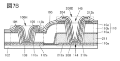
- An embodiment of the present invention includes a first semiconductor layer, a second semiconductor layer, a first conductive layer, a second conductive layer, a third conductive layer, a fourth conductive layer, a fifth conductive layer, a sixth conductive layer, a first insulating layer, a second insulating layer, a third insulating layer, a fourth insulating layer, and a film thickness adjustment layer, the first insulating layer being provided on the first conductive layer and the second conductive layer, and the film thickness adjustment layer being provided on the first insulating layer so as to have an area overlapping with the second conductive layer.
- the first insulating layer has a first opening reaching the first conductive layer in a region overlapping with the first conductive layer
- the first insulating layer and the film thickness adjustment layer have a second opening reaching the second conductive layer in a region overlapping with the second conductive layer
- the third conductive layer is provided on the first insulating layer and has a third opening overlapping with the first opening
- the fourth conductive layer is provided on the film thickness adjustment layer and has a fourth opening overlapping with the second opening
- the insulating layer contacts a side surface of the first insulating layer in the first opening
- the third insulating layer contacts a side surface of the first insulating layer in the second opening and a side surface of the film thickness adjusting layer in the second opening
- the first semiconductor layer contacts an upper surface of the first conductive layer in the first opening, a side surface of the second insulating layer in the first opening, and an upper surface of the third conductive layer
- the second semiconductor layer contacts an upper surface of the second conductive layer in the second opening and a
- the semiconductor device has a sixth conductive layer that contacts the side of the third insulating layer and the top surface of the fourth conductive layer in the first opening, the fourth insulating layer is provided on the first semiconductor layer and the second semiconductor layer, the fifth conductive layer is provided on the fourth insulating layer and faces the first semiconductor layer through the fourth insulating layer in the first opening, and the sixth conductive layer is provided on the fourth insulating layer and faces the second semiconductor layer through the fourth insulating layer in the second opening.
- the first semiconductor layer and the second semiconductor layer contain a metal oxide.
- An aspect of the present invention is to form a first conductive layer and a second conductive layer, form a first insulating film on the first conductive layer and the second conductive layer, form a first layer on the first insulating film so as to have an area overlapping with the second conductive layer, form a conductive film on the first layer and the first insulating film, remove a part of the first insulating film, a part of the first layer, and a part of the conductive film to expose the first conductive layer and the second conductive layer, form a first insulating layer and a third conductive layer each having a first opening in the area overlapping with the first conductive layer, and A first insulating layer, a second layer, and a third conductive layer, each having a second opening, are formed in a region overlapping with the conductive layer, and a second insulating film is formed in contact with an upper surface of the first conductive layer in the first opening, a side surface of the first insulating layer in the first opening, a side surface
- a semiconductor device having a fine-sized transistor and a manufacturing method thereof can be provided.
- a small-sized semiconductor device and a manufacturing method thereof can be provided.
- a semiconductor device having a transistor with a large on-state current and a manufacturing method thereof can be provided.
- a semiconductor device having a transistor with excellent saturation characteristics and a manufacturing method thereof can be provided.
- a semiconductor device having a transistor with a long channel length and a manufacturing method thereof can be provided.
- a semiconductor device having both a transistor with a long channel length and a transistor with a short channel length and a manufacturing method thereof can be provided.
- a semiconductor device having good electrical characteristics and a manufacturing method thereof can be provided.
- a semiconductor device with high reliability and a manufacturing method thereof can be provided.
- a manufacturing method of a semiconductor device with high productivity can be provided.
- a novel semiconductor device and a manufacturing method thereof can be provided.
- FIG. 1A is a plan view of an example of a semiconductor device
- FIG 1B is a cross-sectional view of the example of the semiconductor device.
- FIG. 2 is a cross-sectional view showing an example of a semiconductor device.
- 3A and 3B are cross-sectional views showing an example of a semiconductor device.
- 4A and 4B are cross-sectional views showing an example of a semiconductor device.
- 5A and 5B are cross-sectional views showing an example of a semiconductor device.
- 6A to 6C are cross-sectional views showing an example of a semiconductor device.
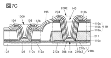
- 7A to 7C are cross-sectional views showing an example of a semiconductor device.
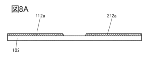
- 8A to 8C are cross-sectional views showing an example of a method for manufacturing a semiconductor device.
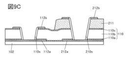
- FIG. 9A to 9C are cross-sectional views showing an example of a method for manufacturing a semiconductor device.
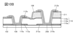
- 10A to 10C are cross-sectional views showing an example of a method for manufacturing a semiconductor device.
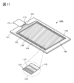
- FIG. 11 is a perspective view showing an example of a display device.
- FIG. 12 is a cross-sectional view showing an example of a display device.
- FIG. 13 is a cross-sectional view showing an example of a display device.
- FIG. 14 is a cross-sectional view showing an example of a display device.
- FIG. 15 is a cross-sectional view showing an example of a display device.
- FIG. 16 is a cross-sectional view showing an example of a display device.
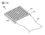
- 17A and 17B are diagrams showing a configuration example of a display device.
- FIG. 18 is a cross-sectional view showing a configuration example of a display device.
- FIG. 19 is a cross-sectional view showing a configuration example of a display device.
- FIG. 20 is a cross-sectional view showing a configuration example of a display device.
- FIG. 21 is a block diagram of a display device.
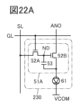
- 22A and 22B are circuit diagrams of a pixel circuit.
- 23A to 23C are circuit diagrams of pixel circuits.
- 24A to 24D are diagrams showing an example of an electronic device.
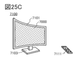
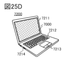
- 25A to 25F are diagrams showing an example of an electronic device.
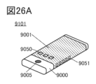
- 26A to 26G are diagrams showing an example of an electronic device.
- film and “layer” can be interchanged depending on the circumstances.
- conductive layer can be changed to the term “conductive film.”
- insulating film can be changed to the term “insulating layer.”
- a transistor is a type of semiconductor element that can perform functions such as amplifying current or voltage, and switching operations that control conduction or non-conduction.
- transistor includes IGFETs (Insulated Gate Field Effect Transistors) and thin film transistors (TFTs).
- source and drain may be interchanged when transistors of different polarity are used, or when the direction of current changes during circuit operation. For this reason, in this specification, the terms “source” and “drain” may be used interchangeably. Note that the source and drain of a transistor may be appropriately referred to as the source terminal and drain terminal, or the source electrode and drain electrode, depending on the situation.
- connection includes “electrical connection.”
- a and B are electrically connected means that, among A and B connected without an insulator (A and B connected via a conductor or semiconductor, or A and B in contact), there is a time when an electrical signal is exchanged or a potential interaction occurs between A and B during circuit operation. In other words, even if there is a time when an electrical signal is not exchanged or a potential interaction does not occur between A and B during circuit operation, if there is a time when an electrical signal is exchanged or a potential interaction occurs between A and B, it can be said that "A and B are electrically connected.”
- Electrical connection includes a connection that does not involve a circuit element (e.g., a transistor, but excluding wiring) (direct connection), and a connection that involves one or more circuit elements (indirect connection).
- a circuit element e.g., a transistor, but excluding wiring
- indirect connection includes a connection that involves one or more circuit elements
- Examples of "A and B being electrically connected” include when A and B are connected without a circuit element, and when A and B are connected via the source and drain of one or more transistors. However, this is subject to the premise that there is a timing when an electrical signal is exchanged or potential interaction occurs between A and B.
- a and B are connected via an insulator and therefore it cannot be said that "A and B are electrically connected" is when there is a dielectric of a capacitive element, a gate insulating film of a transistor, etc. between A and B.
- Examples of cases where A and B are connected without an insulator, but there is no timing when an electrical signal is sent or received between A and B or when potential interaction occurs between A and B, and therefore it cannot be said that "A and B are electrically connected” include a case where a potential V is supplied to the path from A to B from a power source, signal source, etc. (however, this does not include a case where the potential V is supplied via a circuit element), or a case where A and C are connected via the source and drain of a transistor TrP and B and C are connected via the source and drain of a transistor TrQ, but there is no timing when both the transistor TrP and the transistor TrQ are on at the same time.
- SBS Side By Side
- the SBS structure allows the materials and configuration to be optimized for each light-emitting element, which increases the freedom to select materials and configurations and makes it easier to improve brightness and reliability.
- an island-like light-emitting layer refers to a state in which the light-emitting layer is physically separated from the adjacent light-emitting layer.
- a tapered shape refers to a shape in which at least a portion of the side of a structure is inclined with respect to the substrate surface or the surface to be formed.
- it refers to a shape having an area in which the angle (also called the taper angle) between the inclined side and the substrate surface or the surface to be formed is less than 90 degrees.
- the side of the structure, the substrate surface, and the surface to be formed do not necessarily need to be completely flat, and may be approximately planar with a slight curvature, or approximately planar with fine irregularities.
- a step disconnection refers to a phenomenon in which a layer, film, or electrode is disconnected due to the shape of the surface on which it is formed (e.g., a step, etc.).
- top surface shapes shape in plan view, also called contour shape
- contour shape contour in plan view
- the top surface shape of a certain component refers to the contour shape of the component when viewed from a plan view.
- a plan view refers to a view from the normal direction of the surface on which the component is formed, or the surface of the support (e.g., substrate) on which the component is formed.
- approximately the same height refers to a configuration in which the heights from a reference surface (for example, a flat surface such as the surface of a substrate) are approximately the same in a cross-sectional view.
- a planarization process typically a chemical mechanical polishing (CMP) process
- CMP chemical mechanical polishing
- the heights may not strictly match depending on the film material, etc., but in this specification, the heights are also considered to be “approximately the same” in this case.
- One aspect of the present invention is a semiconductor device having a transistor.
- the transistor has a structure in which a source electrode and a drain electrode are provided overlapping each other at different heights with respect to a substrate surface, and a drain current flows in the height direction (vertical direction). Therefore, the transistor can be miniaturized more than a transistor having a structure in which a source electrode and a drain electrode are provided on the same plane.
- the transistor having the above structure can achieve miniaturization and high integration of the semiconductor device.
- the semiconductor device has a first insulating layer sandwiched between a source electrode and a drain electrode of a transistor.
- the first insulating layer has a first opening that reaches one of the source electrode or drain electrode of the transistor, and the other of the source electrode or drain electrode of the transistor has a second opening in a region overlapping with the first opening.
- a second insulating layer is provided in contact with a side surface of the first insulating layer in the first opening
- a semiconductor layer of the transistor is provided in contact with a side surface of the second insulating layer in the first opening, an upper surface of one of the source electrode or drain electrode of the transistor in the first opening, a side surface of the other of the source electrode or drain electrode of the transistor in the second opening, and an upper surface of the other of the source electrode or drain electrode of the transistor. That is, at least a region of the semiconductor layer of the transistor that corresponds to a channel formation region (a region sandwiched between the source electrode and the drain electrode) is in contact with the second insulating layer.
- the second insulating layer contains oxygen, and oxygen can be supplied to the semiconductor layer (particularly, the channel formation region) of the transistor by heat treatment or the like. Therefore, for example, when a metal oxide is used as the material of the semiconductor layer, oxygen vacancies in the metal oxide can be repaired by supplying oxygen from the second insulating layer. Therefore, the electrical characteristics and reliability of the transistor can be improved.
- the semiconductor device may have, in addition to the first insulating layer, a layer (hereinafter also referred to as a film thickness adjustment layer) stacked on or below the first insulating layer between the source electrode and drain electrode of the transistor.
- a layer hereinafter also referred to as a film thickness adjustment layer
- the first insulating layer and the film thickness adjustment layer are located on one of the source electrode or drain electrode of the transistor and below the other of the source electrode or drain electrode of the transistor. Therefore, the channel length of the transistor can be controlled by adjusting the thickness of the first insulating layer and the film thickness adjustment layer.
- the channel length of the transistor can be shortened to the limit resolution of the exposure device or less by forming the first insulating layer thin.
- the channel length of the transistor can be made extremely long. Also, since the channel length direction of the transistor of one embodiment of the present invention corresponds to the vertical direction, the occupation area of the transistor in the substrate surface does not increase due to the channel length.
- transistors with different channel lengths can be formed using some common steps. Therefore, by applying a transistor with a short channel length to a transistor that requires a large on-current and a transistor with a long channel length to a transistor that requires high saturation characteristics (when operating in the saturation region, the magnitude of the drain current hardly changes with an increase in the drain voltage), a high-performance semiconductor device that utilizes the characteristics of each transistor can be realized.
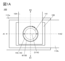
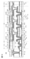
- FIG 1A shows a plan view (also referred to as a top view) of a transistor 100 included in a semiconductor device of one embodiment of the present invention.
- FIG 1B shows a cross-sectional view taken along dashed dotted line A1-A2 in FIG 1A
- FIG 2 shows a cross-sectional view taken along dashed dotted line B1-B2 in FIG 1A.
- some of the components of the transistor 100 are omitted in FIG 1A.
- FIG 1A some of the components are omitted in the plan views of the transistor and the like in the subsequent drawings.
- the transistor 100 is provided on a substrate 102.
- the transistor 100 has a conductive layer 104, an insulating layer 106, a semiconductor layer 108, a conductive layer 112a, and a conductive layer 112b.
- the conductive layer 104 functions as a gate electrode.
- a part of the insulating layer 106 functions as a gate insulating layer.
- the conductive layer 112a functions as one of a source electrode and a drain electrode, and the conductive layer 112b functions as the other of the source electrode and the drain electrode.
- the semiconductor layer 108 the entire region that overlaps with the gate electrode via the gate insulating layer between the source electrode and the drain electrode functions as a channel formation region.
- a region in contact with the source electrode functions as a source region
- a region in contact with the drain electrode functions as a drain region.
- a conductive layer 112a is provided on the substrate 102.
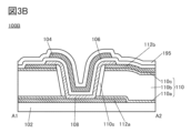
- An insulating layer 110 (insulating layer 110a, insulating layer 110b, and insulating layer 110c) is provided on the conductive layer 112a and on the substrate 102.
- a conductive layer 112b is provided on the insulating layer 110.
- the insulating layer 110 has a region sandwiched between the conductive layer 112a and the conductive layer 112b.
- the conductive layer 112a has a region that overlaps with the conductive layer 112b via the insulating layer 110.
- the insulating layer 110 is shown to have a laminated structure of insulating layer 110a, insulating layer 110b on insulating layer 110a, and insulating layer 110c on insulating layer 110b.
- the insulating layer 110 and the conductive layer 112b each have an opening.
- the opening in the insulating layer 110 is shown as opening 142
- the opening in the conductive layer 112b is shown as opening 143.
- the conductive layer 112a is exposed in opening 142.
- An insulating layer 110s is provided on the conductive layer 112a.
- the insulating layer 110s is provided along the side walls of the opening 142 in the insulating layer 110 and the opening 143 in the conductive layer 112b (i.e., the side of the insulating layer 110 on the opening 142 side and the side of the conductive layer 112b on the opening 143 side).
- the side walls of the opening 142 in the insulating layer 110 and the opening 143 in the conductive layer 112b form a continuous side surface, and the insulating layer 110s is formed along the continuous side surface.
- the insulating layer 110s contacts the upper surface of the conductive layer 112a, the side surface of the insulating layer 110, and the side surface of the conductive layer 112b in the opening 142 and the opening 143.
- the insulating layer 110s may be called a sidewall, a sidewall insulating layer, a sidewall protective layer, or the like.
- the insulating layer 110s is preferably an insulating layer that releases oxygen. As a result, when the insulating layer 110 is made of a material containing oxygen, the oxygen contained in the insulating layer 110 can be supplied to the semiconductor layer 108 through the insulating layer 110s.
- the insulating layer 110s is preferably an insulating layer that contains oxygen.
- the oxygen contained in the insulating layer 110s can be supplied to the semiconductor layer 108.
- oxygen vacancies in the semiconductor layer 108 can be repaired by supplying oxygen from the insulating layer 110s to the semiconductor layer 108, and a transistor having good electrical characteristics and reliability can be realized.
- Opening 142 and opening 143 each have an area that overlaps with conductive layer 112a. Also, opening 142 and opening 143 have an area that overlaps with each other.
- the transistor 100 has a recess (sometimes called a depression) whose bottom is the top surface of the conductive layer 112a and whose inner wall is the side surface (sidewall 141) of the insulating layer 110s.
- the semiconductor layer 108 is provided along the inside of the recess.
- the semiconductor layer 108 overlaps with the conductive layer 112a in a region that is inside the sidewall 141 of the insulating layer 110s in a planar view. In this region, the semiconductor layer 108 contacts the upper surface of the conductive layer 112a.
- the semiconductor layer 108 also overlaps with the conductive layer 112b in a region that is outside the sidewall 141 of the insulating layer 110s in a plan view. In this region, the semiconductor layer 108 contacts the upper surface of the conductive layer 112b.
- the transistor 100 can be said to be a bottom contact type transistor because the bottom surface of the semiconductor layer 108 (the surface facing the substrate 102) is in contact with the source electrode and the drain electrode.
- the semiconductor layer 108 has a region that is provided along the upper surface of the conductive layer 112a, a region that is provided along the sidewall 141 of the insulating layer 110s, and a region that is provided along the upper surface of the conductive layer 112b.
- the semiconductor layer 108 has a region that faces the side of the insulating layer 110 in the opening 142, with the insulating layer 110s sandwiched therebetween. In addition, in this region, the semiconductor layer 108 preferably contacts the sidewall 141 of the insulating layer 110s.
- An insulating layer 106 is provided on the semiconductor layer 108.
- the insulating layer 106 has a region that overlaps with the conductive layer 112a with the semiconductor layer 108 sandwiched therebetween, a region that faces the insulating layer 110 with the semiconductor layer 108 and the insulating layer 110s sandwiched therebetween, a region that faces the conductive layer 112b with the semiconductor layer 108 and the insulating layer 110s sandwiched therebetween, and a region that overlaps with the conductive layer 112b with the semiconductor layer 108 sandwiched therebetween.
- the insulating layer 106 has a region facing the top surface of the conductive layer 112a with the semiconductor layer 108 sandwiched therebetween, a region facing the side surface of the insulating layer 110 with the semiconductor layer 108 and the insulating layer 110s sandwiched therebetween, a region facing the side surface of the conductive layer 112b with the semiconductor layer 108 and the insulating layer 110s sandwiched therebetween, and a region facing the top surface of the conductive layer 112b with the semiconductor layer 108 sandwiched therebetween.
- a conductive layer 104 is provided on the insulating layer 106.
- the conductive layer 104 has a region facing the semiconductor layer 108 between the conductive layer 112a and the conductive layer 112b, with the insulating layer 106 sandwiched therebetween.
- the conductive layer 104 and the conductive layer 112a are insulated by the insulating layer 106 provided therebetween.
- the conductive layer 104 and the conductive layer 112b are insulated by the insulating layer 106 provided therebetween.
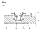
- the transistor 100 has a recess.
- the bottom of the recess is the top surface of the conductive layer 112a, and the inner wall is the side wall 141 of the insulating layer 110s.
- the semiconductor layer 108 is provided along the inside of the recess and has a shape corresponding to the recess.
- the insulating layer 106 is provided on the semiconductor layer 108 and has a shape corresponding to the recess.
- the conductive layer 104 is provided on the insulating layer 106. Note that, although FIG. 1B and other figures show an example in which the conductive layer 104 has a shape that conforms to the recess, this is not the only possible example.
- the conductive layer 104 can also be provided so as to fill the recesses on the semiconductor layer 108 and the insulating layer 106 that reflect the shape along the side surface of the insulating layer 110s and the top surface of the conductive layer 112a. This allows the conductive layer 104 to be thickened, thereby reducing the electrical resistance.
- An insulating layer 195 is provided to cover the conductive layer 112a, the semiconductor layer 108, the conductive layer 112b, the insulating layer 106, the conductive layer 104, etc., of the transistor 100.
- the insulating layer 195 functions as a protective layer for the transistor 100.
- the upper surface shape of the openings 142 and 143 may be, for example, circular or elliptical.
- the upper surface shape of the openings 142 and 143 may be polygonal, such as a triangle, a quadrangle (including a rectangle, a rhombus, and a square), or a pentagon, or a polygon with rounded corners.
- the upper surface shape of the openings 142 and 143 is preferably circular.
- the shape of the top surface of the sidewall 141 of the insulating layer 110s changes according to the shape of the opening 142 in the insulating layer 110 and the opening 143 in the conductive layer 112b.
- the top surface of the sidewall 141 can be made annular.
- the uniformity of the film thickness of the semiconductor layer 108 provided along the sidewall 141 can be improved.
- the top surface of the sidewall 141 has a corner, for example, the film thickness of the semiconductor layer 108 and the film thickness of the insulating layer 106 formed on the semiconductor layer 108 may be non-uniform compared to when the top surface does not have a corner.
- the opening 142 in the insulating layer 110 and the opening 143 in the conductive layer 112b can be formed, for example, by forming a mask on the surface to be processed and then using an etching process.
- the mask may be a resist mask or a hard mask made of an insulating layer or a conductive layer.
- the opening 143 in the conductive layer 112b and the opening 142 in the insulating layer 110 are successively formed, so that the mask formation process and each opening formation process can be performed consecutively.
- the diameter and position of each opening can also be made to match or approximately match. In this specification, the process of successively forming multiple openings using the same mask is sometimes called a batch opening.
- the insulating layer 110s is formed, thereby making it possible to fabricate the configuration shown in FIG. 1B, FIG. 2, etc.
- the diameters of the openings are made to match or roughly match, thereby improving the coverage of the insulating layer 110s.
- the opening 142 in the insulating layer 110 and the opening 143 in the conductive layer 112b do not have to be formed consecutively.
- a mask may be formed when each opening is provided.
- the channel length and channel width of transistor 100 are explained.
- the region in contact with the conductive layer 112a functions as one of the source region and the drain region
- the region in contact with the conductive layer 112b functions as the other of the source region and the drain region
- the region between the source region and the drain region functions as a channel formation region.
- the channel length of the transistor 100 is the distance between the source region and the drain region. Therefore, the channel length can be said to be the distance between the conductive layer 112a and the conductive layer 112b along the interface between the semiconductor layer 108 and the insulating layer 110s.
- the channel length may also be defined as the distance between the top surface of the conductive layer 112a and the top surface of the conductive layer 112b in the direction along the interface between the semiconductor layer 108 and the insulating layer 110s.
- the channel length of the transistor 100 is described as the distance between the top surface of the conductive layer 112a and the top surface of the conductive layer 112b along the interface between the semiconductor layer 108 and the insulating layer 110s.
- the channel length L100 of the transistor 100 is indicated by a double-headed dashed arrow.
- the channel length L100 of the transistor 100 may be represented by a thickness T110, which is the thickness of the insulating layer 110 in the region between the upper surface of the conductive layer 112a and the lower surface of the conductive layer 112b.
- the channel length L100 of the transistor 100 may be represented by the sum of the thickness T110 and the thickness of the conductive layer 112b.
- the thickness T110 is indicated by a dashed double-headed arrow.
- the channel length L100 of the transistor 100 is determined by the thickness of the insulating layer 110, the angle ⁇ 110 between the surface on which the insulating layer 110s is formed (here, the side surface of the insulating layer 110) and the surface on which the insulating layer 110 is formed (here, the top surface of the conductive layer 112a), and the like, and is not affected by the performance of the exposure device used to fabricate the transistor. Therefore, the channel length L100 can be set to a value smaller than the limit resolution of the exposure device, making it possible to realize a transistor of a fine size.
- the channel length L100 can be increased, and a transistor with a long channel length can be realized.
- the longer the channel length the greater the area occupied by the transistor in a planar view, making it difficult to manufacture a semiconductor device with a high degree of integration.
- the channel length corresponds to the thickness direction of the insulating layer 110, so the area occupied by the transistor in a planar view does not increase depending on the channel length. Therefore, even if a transistor with a long channel length is included, a semiconductor device with a high degree of integration can be realized.
- the channel length of the transistor 100 is not restricted by the integration degree of the semiconductor device, a transistor with a longer channel length than a planar transistor can be applied to the semiconductor device.
- the channel length L100 can be, for example, 5 nm or more and less than 3 ⁇ m, 7 nm or more and less than 2.5 ⁇ m, 10 nm or more and less than 2 ⁇ m, 10 nm or more and less than 1.5 ⁇ m, 10 nm or more and less than 1.2 ⁇ m, 10 nm or more and less than 1 ⁇ m, 10 nm or more and less than 500 nm, 10 nm or more and less than 300 nm, 10 nm or more and less than 200 nm, 10 nm or more and less than 100 nm, 10 nm or more and less than 50 nm, 10 nm or more and less than 30 nm, or 10 nm or more and less than 20 nm.
- the channel length L100 can be 100 nm or more and less than 1 ⁇ m.
- the thickness T110 can be, for example, 5 nm or more and less than 3 ⁇ m, 7 nm or more and less than 2.5 ⁇ m, 10 nm or more and less than 2 ⁇ m, 10 nm or more and less than 1.5 ⁇ m, 10 nm or more and less than 1.2 ⁇ m, 10 nm or more and less than 1 ⁇ m, 10 nm or more and less than 500 nm, 10 nm or more and less than 300 nm, 10 nm or more and less than 200 nm, 10 nm or more and less than 100 nm, 10 nm or more and less than 50 nm, 10 nm or more and less than 30 nm, or 10 nm or more and less than 20 nm.
- the thickness T110 can be set appropriately to obtain the desired channel length L100.
- the angle ⁇ 110 can be, for example, 30 degrees or more and 90 degrees or less, 35 degrees or more and 85 degrees or less, 40 degrees or more and 80 degrees or less, 45 degrees or more and 80 degrees or less, 50 degrees or more and 80 degrees or less, 55 degrees or more and 80 degrees or less, 60 degrees or more and 80 degrees or less, 65 degrees or more and 80 degrees or less, or 70 degrees or more and 80 degrees or less.
- the angle ⁇ 110 can be appropriately set to obtain the desired channel length L100.
- the smaller the value of the angle ⁇ 110 i.e., the more tapered the side surface of the insulating layer 110 is in the opening 142), the higher the coverage of the film (e.g., the semiconductor layer 108) formed to cover the side surface can be, which is preferable.
- the closer the angle ⁇ 110 is to 90 degrees i.e., the closer the side surface of the insulating layer 110 is to being perpendicular to the substrate surface in the opening 142
- the insulating layer 110s is provided along the entire region of each sidewall of the opening 142 of the insulating layer 110 and the opening 143 of the conductive layer 112b, but this is not the only possible example.
- the height of the upper end of the insulating layer 110s may be lower than the height of the upper surface of the conductive layer 112b, and the insulating layer 110s may not cover a part of the side surface of the conductive layer 112b in the opening 143. It is preferable that the insulating layer 110s covers at least the entire side surface of the insulating layer 110 in the opening 142.
- the on-current of the transistor 100 can be increased.
- the saturation characteristics of the on-current of the transistor 100 can be improved. Therefore, by appropriately adjusting the channel length, a transistor 100 with desired characteristics can be realized. Furthermore, by applying the transistor 100, it is possible to reduce the area occupied by the circuit in the semiconductor device compared to the case where a planar type transistor is applied, and the semiconductor device can be made more compact.
- the frame of the display device can be narrowed.
- a transistor of one embodiment of the present invention when applied to a large display device or a high-resolution display device, even if the number of wirings is increased, signal delay in each wiring can be reduced, and display unevenness can be suppressed.
- the channel width of the transistor 100 is the length of the source region or the length of the drain region in a planar view.
- the channel width is the length of the region where the semiconductor layer 108 and the conductive layer 112a contact each other, or the length of the region where the semiconductor layer 108 and the conductive layer 112b contact each other in a planar view.
- the semiconductor layer 108 is provided along a recess whose bottom is the top surface of the conductive layer 112a and whose inner wall is the side wall 141 of the insulating layer 110s. Therefore, the perimeter of the inner wall of the recess in a planar view may be used as the channel width.
- the insulating layer 110s can also be expressed as having a shape with an opening at or near the center of a cylinder in a planar view. The perimeter of the opening can also be used as the channel width of the semiconductor layer 108.
- the channel width of the transistor 100 is described as the length of the region where the semiconductor layer 108 and the conductive layer 112b contact each other in a planar view.
- the channel width W100 of the transistor 100 is indicated by a solid double-headed arrow.
- the channel width W100 is the perimeter of the opening 143 in a planar view.
- the channel width W100 is determined by the top surface shape of the opening 143.
- the width D143 of the opening 143 is indicated by a two-dot chain line with a double arrow.
- the width D143 refers to the short side of the smallest rectangle that circumscribes the opening 143 in a plan view.
- the width D143 of the opening 143 is equal to or greater than the limit resolution of the exposure device.
- the width D143 is, for example, 0.20 ⁇ m or more and less than 5.0 ⁇ m.
- the width D143 corresponds to the diameter of the opening 143, and the channel width W100 can be calculated as "D143 x ⁇ ".
- the semiconductor material that can be used for the semiconductor layer 108 is not particularly limited.
- an elemental semiconductor or a compound semiconductor can be used.
- the elemental semiconductor for example, silicon or germanium can be used.
- the compound semiconductor for example, gallium arsenide and silicon germanium can be used.
- an organic substance having semiconductor properties or a metal oxide (also referred to as an oxide semiconductor) having semiconductor properties can be used. Note that these semiconductor materials may contain impurities as dopants.
- the crystallinity of the semiconductor material used for the semiconductor layer 108 is not particularly limited, and any of an amorphous semiconductor and a semiconductor having crystallinity (a single crystal semiconductor, a polycrystalline semiconductor, a microcrystalline semiconductor, or a semiconductor having a crystalline region in a portion) may be used.
- the use of a semiconductor having crystallinity is preferable because it can suppress deterioration of the transistor characteristics.
- Silicon can be used for the semiconductor layer 108.
- Examples of silicon include single crystal silicon, polycrystalline silicon, microcrystalline silicon, and amorphous silicon.
- Examples of polycrystalline silicon include low temperature polysilicon (LTPS).
- Transistors using amorphous silicon for the semiconductor layer 108 can be formed on large glass substrates and can be manufactured at low cost. Transistors using polycrystalline silicon for the semiconductor layer 108 have high field effect mobility and can operate at high speed. Transistors using microcrystalline silicon for the semiconductor layer 108 have higher field effect mobility and can operate at high speed than transistors using amorphous silicon.
- the semiconductor layer 108 preferably has a metal oxide (oxide semiconductor).
- metal oxides that can be used for the semiconductor layer 108 include indium oxide, gallium oxide, and zinc oxide.
- the metal oxide preferably contains at least indium (In) or zinc (Zn).
- the metal oxide preferably contains two or three elements selected from indium, element M, and zinc.
- the element M is one or more elements selected from gallium, aluminum, silicon, boron, yttrium, tin, copper, vanadium, beryllium, titanium, iron, nickel, germanium, zirconium, molybdenum, lanthanum, cerium, neodymium, hafnium, tantalum, tungsten, cobalt, and magnesium.
- the element M is preferably one or more elements selected from aluminum, gallium, yttrium, and tin.
- the element M is more preferably gallium.
- indium tin oxide containing silicon can be used.
- the metal oxide can be formed preferably by sputtering or atomic layer deposition (ALD).
- ALD atomic layer deposition
- the atomic ratio of the target and the atomic ratio of the metal oxide may differ.
- the atomic ratio of zinc in the metal oxide may be smaller than the atomic ratio of the target.
- the atomic ratio of zinc in the metal oxide may be 40% or more and 90% or less of the atomic ratio of zinc contained in the target.
- Specific examples of forming the semiconductor layer 108 by the ALD method include film formation methods such as thermal ALD and PEALD (Plasma Enhanced ALD).
- the thermal ALD method is preferred because it exhibits extremely high step coverage.
- the PEALD method is also preferred because it exhibits high step coverage and allows low-temperature film formation.
- composition of the metal oxide in the semiconductor layer 108 significantly affects the electrical characteristics and reliability of the transistor 100.
- a transistor with a large on-state current can be realized.
- a transistor with high reliability when a positive bias is applied can be realized.
- a transistor with high reliability when a positive bias is applied can be realized.
- a transistor with high reliability when a positive bias is applied can be realized.
- a transistor with high reliability when exposed to light can be realized.
- the semiconductor layer 108 is preferably a crystalline metal oxide layer.
- a metal oxide layer having a CAAC (C-Axis Aligned Crystal) structure, a polycrystalline (poly-crystal) structure, a nanocrystalline (nc: nano-crystal) structure, or the like can be used.
- the CAAC structure is a crystal structure in which multiple microcrystals (typically multiple IGZO microcrystals) have a c-axis orientation, and the multiple microcrystals are connected without being oriented in the a-b plane.
- the CAAC structure has fewer crystal grain boundaries and grains in the a-b plane than the polycrystalline structure, and therefore a highly reliable transistor can be realized.
- the semiconductor layer 108 may have a stacked structure of two or more metal oxide layers with different crystallinity.
- a stacked structure of a first metal oxide layer and a second metal oxide layer provided on the first metal oxide layer may be used, and the second metal oxide layer may have a region with higher crystallinity than the first metal oxide layer.
- the second metal oxide layer may have a region with lower crystallinity than the first metal oxide layer.
- the two or more metal oxide layers in the semiconductor layer 108 may have the same or approximately the same composition. By forming a stacked structure of metal oxide layers with the same composition, for example, the same sputtering target can be used to form the layers, which can reduce manufacturing costs.
- a stacked structure of two or more metal oxide layers with different crystallinity can be formed.
- the two or more metal oxide layers in the semiconductor layer 108 may have different compositions.
- the thickness of the semiconductor layer 108 is preferably 3 nm or more and 100 nm or less, more preferably 5 nm or more and 100 nm or less, even more preferably 10 nm or more and 100 nm or less, even more preferably 10 nm or more and 70 nm or less, even more preferably 15 nm or more and 70 nm or less, even more preferably 15 nm or more and 50 nm or less, even more preferably 20 nm or more and 50 nm or less, even more preferably 20 nm or more and 40 nm or less, even more preferably 25 nm or more and 40 nm or less.
- oxygen vacancies may be formed in the oxide semiconductor.
- VOH oxygen vacancies
- some of the hydrogen may bond with oxygen bonded to a metal atom to generate an electron that is a carrier. Therefore, a transistor using an oxide semiconductor containing a large amount of hydrogen is likely to have normally-on characteristics. Furthermore, hydrogen in an oxide semiconductor is easily moved by stress such as heat or an electric field, and therefore, if an oxide semiconductor contains a large amount of hydrogen, the reliability of the transistor may be deteriorated.
- VOH can function as a donor of an oxide semiconductor.
- evaluation may be performed using the carrier concentration instead of the donor concentration.
- the carrier concentration assuming a state in which no electric field is applied may be used instead of the donor concentration.
- the "carrier concentration” described in this specification and the like may be rephrased as the "donor concentration”.
- V O H when an oxide semiconductor is used for the semiconductor layer 108, it is preferable to reduce V O H in the semiconductor layer 108 as much as possible and make the semiconductor layer 108 highly pure and intrinsic or substantially highly pure and intrinsic.
- it is important to remove impurities such as water and hydrogen from the oxide semiconductor (sometimes referred to as dehydration or dehydrogenation treatment) and to supply oxygen to the oxide semiconductor to repair oxygen vacancies (V O ).
- an oxide semiconductor with sufficiently reduced defects such as V O H for a channel formation region of a transistor, stable electrical characteristics can be imparted.
- oxygen addition treatment supplying oxygen to an oxide semiconductor to repair oxygen vacancies (V O ) may be referred to as oxygen addition treatment.
- the carrier concentration of the oxide semiconductor in a region functioning as a channel formation region is preferably 1 ⁇ 10 18 cm -3 or less, more preferably less than 1 ⁇ 10 17 cm -3 , further preferably less than 1 ⁇ 10 16 cm -3 , further preferably less than 1 ⁇ 10 13 cm -3 , and further preferably less than 1 ⁇ 10 12 cm -3 .
- the lower limit of the carrier concentration of the oxide semiconductor in the region functioning as a channel formation region is not particularly limited, and can be, for example, 1 ⁇ 10 -9 cm -3 .
- Transistors using an oxide semiconductor have extremely high field-effect mobility compared to transistors using amorphous silicon.
- the leakage current between the source and drain of an OS transistor in an off state (hereinafter also referred to as off-current) is extremely small, and the charge accumulated in a capacitor connected in series with the transistor can be held for a long period of time.
- off-current the leakage current between the source and drain of an OS transistor in an off state
- OS transistors can be applied to display devices. To increase the emission luminance of a light-emitting element included in a pixel circuit of a display device, it is necessary to increase the amount of current flowing through the light-emitting element. To achieve this, it is necessary to increase the source-drain voltage of a driving transistor included in the pixel circuit. Compared to transistors using silicon (hereinafter referred to as Si transistors), OS transistors have a higher source-drain withstand voltage, so a high voltage can be applied between the source and drain of an OS transistor. Therefore, by applying an OS transistor to a driving transistor in a pixel circuit, it is possible to increase the amount of current flowing through the light-emitting element and increase the emission luminance of the light-emitting element.
- an OS transistor When a transistor operates in the saturation region, an OS transistor can reduce the change in source-drain current in response to a change in gate-source voltage compared to a Si transistor. Therefore, by using an OS transistor as a driving transistor included in a pixel circuit, the current flowing between the source and drain can be precisely determined by changing the gate-source voltage, and the amount of current flowing to the light-emitting element can be precisely controlled. This allows a greater number of gray levels to be achieved in the pixel circuit.
- an OS transistor can pass a more stable current (saturation current) than a Si transistor, even when the source-drain voltage gradually increases. Therefore, by using an OS transistor as a driving transistor, a stable current can be passed to the light-emitting element, for example, even when there is variation in the current-voltage characteristics of the light-emitting element. In other words, when an OS transistor operates in the saturation region, the source-drain current hardly changes even when the source-drain voltage is increased, so the light emission luminance of the light-emitting element can be stabilized.
- OS transistors have small variations in electrical characteristics due to radiation exposure, i.e., they have high resistance to radiation, and therefore can be suitably used in environments where radiation may be present. It can also be said that OS transistors have high reliability against radiation.
- OS transistors can be suitably used in pixel circuits of X-ray flat panel detectors.
- OS transistors can also be suitably used in semiconductor devices used in outer space.
- radiation include electromagnetic radiation (e.g., X-rays and gamma rays) and particle radiation (e.g., alpha rays, beta rays, neutron rays, and proton rays).
- an inorganic insulating material or an organic insulating material can be used for the insulating layer.
- a stacked structure of an inorganic insulating material and an organic insulating material may be used for the insulating layer.
- inorganic insulating materials one or more of oxide, oxynitride, oxynitride, and nitride can be used.
- an oxynitride refers to a material whose composition contains more oxygen than nitrogen.
- a nitride oxide refers to a material whose composition contains more nitrogen than oxygen.
- silicon oxynitride refers to a material whose composition contains more oxygen than nitrogen
- silicon nitride oxide refers to a material whose composition contains more nitrogen than oxygen.
- SIMS secondary ion mass spectrometry
- XPS X-ray photoelectron spectrometry
- SIMS is suitable when the content of the target element is high (e.g., 0.5 atomic% or more, or 1 atomic% or more).
- SIMS is suitable when the content of the target element is low (e.g., less than 0.5 atomic% or less than 1 atomic%).
- the film density of the insulating layer can be evaluated, for example, by Rutherford Backscattering Spectrometry (RBS) or X-ray Reflection (XRR). Differences in film density can sometimes be evaluated in cross-sectional transmission electron microscopy (TEM) images. In TEM observation, if the film density is high, the transmission electron (TE) image becomes dense (dark), and if the film density is low, the transmission electron (TE) image becomes faint (bright). Even when the same material is used for the insulating layer, if the film densities are different, the boundaries between these can sometimes be observed as differences in contrast in the cross-sectional TEM image.
- TEM transmission electron microscopy
- the nitrogen content of the insulating layer can be confirmed, for example, by energy dispersive X-ray spectrometry (EDX).
- EDX energy dispersive X-ray spectrometry
- the nitrogen content can be evaluated using the ratio of the nitrogen peak height to the silicon peak height.
- the peak of a certain element refers to the point at which the count number of the element is a maximum value in a spectrum in which the horizontal axis shows the energy of characteristic X-rays and the vertical axis shows the count number (detection value) of characteristic X-rays.
- the count number at the energy of characteristic X-rays specific to the element can be used to confirm the difference in nitrogen content by the ratio of the nitrogen count number to the silicon count number.
- the count number at 1.739 keV (Si-K ⁇ ) can be used for silicon
- the count number at 0.392 keV (N-K ⁇ ) can be used for nitrogen.
- the hydrogen concentration in the insulating layer can be evaluated, for example, by SIMS.
- oxygen can be supplied from the insulating layer to the semiconductor layer 108.
- oxygen vacancies ( VO ) and VOH in the semiconductor layer 108 can be reduced, and a transistor with good electrical characteristics and high reliability can be obtained.
- other treatments for supplying oxygen to the semiconductor layer 108 include heat treatment in an atmosphere containing oxygen, plasma treatment in an atmosphere containing oxygen, and the like.
- oxygen vacancies ( VO ) may be formed in the semiconductor layer 108.
- VOH may be formed in the semiconductor layer 108, and the carrier concentration in the semiconductor layer 108 may be increased.
- the oxygen vacancies (V O ) and V O H in the channel formation region of the transistor 100 are small.
- the oxygen vacancies (V O ) and V O H in the channel formation region have a large effect on the electrical characteristics and reliability of the transistor 100.
- the diffusion of V O H from the source region or drain region to the channel formation region increases the carrier concentration in the channel formation region, which may cause a change in the threshold voltage of the transistor 100 or a decrease in reliability.
- the shorter the channel length L100 of the transistor 100 the larger the effect of such diffusion of V O H on the electrical characteristics and reliability of the transistor 100.
- the insulating layer in contact with the semiconductor layer 108 or the insulating layer located around the semiconductor layer 108 releases little impurities (e.g., water and hydrogen) from itself.
- impurities e.g., water and hydrogen
- Oxygen may be released from the semiconductor layer 108 due to heat applied in a step after the formation of the semiconductor layer 108.
- oxygen is supplied to the semiconductor layer 108 from an insulating layer in contact with the semiconductor layer 108 or an insulating layer located around the semiconductor layer 108, so that an increase in oxygen vacancies ( VO ) and VOH in the semiconductor layer 108 can be suppressed.
- the degree of freedom in the process temperature can be increased in the steps after the formation of the semiconductor layer 108. Specifically, the process temperature can be increased in the steps after the formation of the semiconductor layer 108. Therefore, the transistor 100 exhibits favorable electrical characteristics and is highly reliable.
- Insulating layer 110 An inorganic insulating material or an organic insulating material can be used for the insulating layer 110.
- the insulating layer 110 may have a stacked structure of an inorganic insulating material and an organic insulating material.
- An inorganic insulating material can be suitably used as the insulating layer 110.
- the inorganic insulating material one or more of oxide, oxynitride, nitride oxide, and nitride can be used.
- the insulating layer 110 for example, one or more of silicon oxide, silicon oxynitride, aluminum oxide, hafnium oxide, yttrium oxide, zirconium oxide, gallium oxide, tantalum oxide, magnesium oxide, lanthanum oxide, cerium oxide, neodymium oxide, silicon nitride, silicon nitride oxide, and aluminum nitride can be used.
- the insulating layer 110 may have a laminated structure of two or more layers.
- FIG. 1B and other figures show that the insulating layer 110 has a laminated structure of an insulating layer 110a, an insulating layer 110b on the insulating layer 110a, and an insulating layer 110c on the insulating layer 110b.
- the insulating layers 110a, 110b, and 110c may each be made of the materials that can be used for the insulating layer 110 described above. Note that the insulating layers 110a, 110b, and 110c may each be made of the same material or different materials.
- each of insulating layers 110a, 110b, and 110c emits little impurities (e.g., water and hydrogen) from itself.
- the thickness of insulating layer 110b can be configured to be thicker than the thickness of insulating layer 110a and the thickness of insulating layer 110c.
- the deposition rate of insulating layer 110b is preferably faster than the deposition rate of insulating layer 110a and the deposition rate of insulating layer 110c.
- Insulating layer 110a and insulating layer 110c each function as a blocking film that suppresses gas escaping from insulating layer 110b.
- insulating layer 110a and insulating layer 110c it is preferable to use a material through which gas does not easily diffuse. It is preferable that insulating layer 110a and insulating layer 110c each have an area with a higher film density than insulating layer 110b.
- By increasing the film density of the insulating layer it is possible to increase the blocking ability against gas. By slowing down the film formation speed of the insulating layer, the film density increases and the blocking ability against gas can be increased.
- an oxide or an oxynitride as the insulating layer 110b. It is preferable to use a film that releases oxygen when heated as the insulating layer 110b.
- silicon oxide or silicon oxynitride can be suitably used as the insulating layer 110b.
- oxygen can be supplied from the insulating layer 110b to the semiconductor layer 108.
- the insulating layer 110b has a high oxygen diffusion coefficient. By increasing the oxygen diffusion coefficient, oxygen can be easily diffused in the insulating layer 110b, and oxygen can be efficiently supplied to the semiconductor layer 108.
- the insulating layer 110b by configuring the insulating layer 110b to be thicker than the insulating layer 110a and the insulating layer 110c, more oxygen can be supplied to the semiconductor layer 108.
- Insulating layers 110a, 110b, and 110c are preferably formed by a film formation method such as sputtering, ALD, or plasma CVD.
- the film by forming the film by a sputtering method without using a gas containing hydrogen in the film forming gas, a film with an extremely low hydrogen content can be obtained. Therefore, hydrogen can be prevented from being supplied to the semiconductor layer 108, and the electrical characteristics of the transistor 100 can be stabilized.
- the film When forming a silicon oxide film by a sputtering method, the film can be formed, for example, using a silicon target in an atmosphere containing an oxygen gas.
- the film when forming a silicon nitride film by a sputtering method, the film can be formed, for example, using a silicon target in an atmosphere containing nitrogen gas.
- the film When forming an aluminum oxide film by a sputtering method, the film can be formed, for example, using an aluminum target in an atmosphere containing an oxidizing gas.
- Silicon oxide and silicon nitride can be deposited using, for example, the PEALD method.
- Aluminum oxide and hafnium oxide can be deposited using, for example, the thermal ALD method.
- a dense insulating film can be formed, which can improve blocking properties against oxygen and hydrogen.
- the insulating layers 110a and 110c can be made of a material with a higher nitrogen content than the insulating layer 110b. Increasing the nitrogen content of the insulating layer can improve the blocking properties against oxygen and hydrogen.
- insulating layer 110a and insulating layer 110c may have regions in which the hydrogen concentration in the film is lower than that of insulating layer 110b.
- the insulating layer 110a and the insulating layer 110c are preferably impermeable to oxygen. Furthermore, the insulating layer 110a and the insulating layer 110c are preferably impermeable to hydrogen.
- the insulating layer 110a and the insulating layer 110c function as blocking films that suppress the diffusion of hydrogen from the outside of the transistor to the semiconductor layer 108 through the insulating layer 110a and the insulating layer 110c.
- the film density of the insulating layer 110a and the insulating layer 110c is preferably higher than the film density of the insulating layer 110b. By increasing the film density of the insulating layer, the blocking property of oxygen and hydrogen can be improved.
- silicon oxide or silicon oxynitride is used for the insulating layer 110b
- silicon nitride or silicon nitride oxide can be used for the insulating layer 110a and the insulating layer 110c, respectively.
- hafnium oxide or aluminum oxide can be suitably used for the insulating layer 110a and the insulating layer 110c.
- insulating layer 110a and insulating layer 110c may each have a structure in which two or more materials selected from silicon nitride, silicon oxynitride, hafnium oxide, and aluminum oxide are stacked.
- the amount of oxygen supplied from the insulating layer 110b to the semiconductor layer 108 may decrease.
- the insulating layer 110a below the insulating layer 110b it is possible to suppress the oxygen contained in the insulating layer 110b from diffusing downward from the insulating layer 110b.
- the insulating layer 110c on the insulating layer 110b it is possible to suppress the oxygen contained in the insulating layer 110b from diffusing upward from the insulating layer 110b. Therefore, the amount of oxygen supplied from the insulating layer 110b to the semiconductor layer 108 increases, and oxygen vacancies ( VO ) and VOH in the semiconductor layer 108 can be reduced.
- the conductive layer 112a and the conductive layer 112b may be oxidized by oxygen contained in the insulating layer 110b, and the resistance may be increased.
- the amount of oxygen supplied from the insulating layer 110b to the semiconductor layer 108 may be reduced by the oxidation of the conductive layer 112a and the conductive layer 112b.
- the conductive layer 112a and the conductive layer 112b may be prevented from being oxidized and the resistance may be reduced.
- the amount of oxygen supplied from the insulating layer 110b to the semiconductor layer 108 can be increased, and oxygen vacancies ( VO ) and VOH in the semiconductor layer 108 can be reduced.
- the insulating layers 110a and 110c Furthermore, by providing the insulating layers 110a and 110c, diffusion of hydrogen into the semiconductor layer 108 can be suppressed, and oxygen vacancies ( VO ) and VOH in the semiconductor layer 108 can be reduced.
- the insulating layer 110a and the insulating layer 110c each preferably have a thickness that functions as a blocking film for oxygen and hydrogen. If the film thickness is too thin, the function as a blocking film may be reduced. On the other hand, if the film thickness is too thick, the region of the semiconductor layer 108 facing the insulating layer 110b may become narrow, and the amount of oxygen supplied to the semiconductor layer 108 may become small.
- the film thicknesses (film thicknesses with respect to the surface to be formed) of the insulating layer 110a and the insulating layer 110c are preferably 1 nm or more and 200 nm or less, 1 nm or more and 100 nm or less, 1 nm or more and 60 nm or less, 1 nm or more and 50 nm or less, 1 nm or more and 40 nm or less, 1 nm or more and 30 nm or less, 1 nm or more and 20 nm or less, 1 nm or more and 10 nm or less, 1 nm or more and 5 nm or less, or 2 nm or more and 5 nm or less.
- an organic insulating material may be used as the insulating layer 110.
- a material that releases oxygen is used for the insulating layer 110s in contact with the semiconductor layer 108. Therefore, even if a material that releases oxygen is not used for the insulating layer 110 (for example, even if an organic insulating material is used), oxygen can be supplied from the insulating layer 110s to the semiconductor layer 108. Therefore, in one embodiment of the present invention, an organic insulating material such as a resin that can be formed by coating or the like can also be used for the insulating layer 110.
- Organic insulating materials that can be used for the insulating layer 110 include acrylic resin, polyimide resin, epoxy resin, polyamide resin, polyimideamide resin, siloxane resin, benzocyclobutene resin, phenolic resin, precursors of these resins, etc.
- the insulating layer 110 may have a laminated structure of an organic insulating film and an inorganic insulating film.
- the insulating layer 106 functioning as a gate insulating layer and the insulating layer 110s functioning as a sidewall insulating layer preferably have a low defect density. Both the insulating layer 106 and the insulating layer 110s are layers in contact with the semiconductor layer 108. Thus, the low defect density of the insulating layer 106 and the insulating layer 110s allows a transistor to have good electrical characteristics. Furthermore, the insulating layer 106 and the insulating layer 110s preferably have a high withstand voltage. The high withstand voltage of the insulating layer 106 and the insulating layer 110s allows a transistor to have high reliability.
- the insulating layer 106 and the insulating layer 110s may each be made of, for example, one or more of an oxide, an oxide nitride, a nitride oxide, and a nitride having insulating properties.
- the insulating layer 106 and the insulating layer 110s may each be made of, for example, one or more of silicon oxide, silicon oxide nitride, silicon nitride, aluminum oxide, aluminum oxide nitride, aluminum nitride, aluminum oxide, hafnium oxide, hafnium oxynitride, gallium oxide, gallium oxide nitride, yttrium oxide, yttrium oxynitride, and Ga-Zn oxide.
- the insulating layer 106 and the insulating layer 110s may each be a single layer or a stacked layer.
- the insulating layer 106 and the insulating layer 110s may each be a stacked layer structure of an oxide and a nitride, for example.
- the leakage current may become large.
- a material with a high relative dielectric constant also called a high-k material
- high-k materials include gallium oxide, hafnium oxide, zirconium oxide, oxides containing aluminum and hafnium, oxynitrides containing aluminum and hafnium, oxides containing silicon and hafnium, oxynitrides containing silicon and hafnium, and nitrides containing silicon and hafnium.
- the insulating layer 106 and the insulating layer 110s release little impurities (e.g., water and hydrogen) from themselves. By reducing the release of impurities from the insulating layer 106 and the insulating layer 110s, the impurities are prevented from diffusing into the semiconductor layer 108, and a transistor exhibiting good electrical characteristics and high reliability can be obtained.
- impurities e.g., water and hydrogen
- the insulating layer 106 is a film formed under conditions that cause little damage to the semiconductor layer 108.
- the insulating layer 106 is formed under conditions in which the film formation speed (also called the film formation rate) is sufficiently slow.
- the film formation speed also called the film formation rate
- the damage to the semiconductor layer 108 can be reduced by forming the insulating layer 106 under low power conditions.
- the insulating layer 106 and the insulating layer 110s using an example of a configuration in which a metal oxide is used for the semiconductor layer 108.
- an oxide and an oxynitride on at least the side of the insulating layer 106 and the insulating layer 110s that contacts the semiconductor layer 108.
- one or more of silicon oxide and silicon oxynitride can be suitably used for the insulating layer 106 and the insulating layer 110s. It is more preferable to use a film that releases oxygen when heated for the insulating layer 106 and the insulating layer 110s.
- the insulating layer 106 and the insulating layer 110s may have a stacked structure.
- the insulating layer 106 can have a stacked structure of an oxide film or oxynitride film on the side in contact with the semiconductor layer 108 and a nitride film on the side in contact with the conductive layer 104.
- the insulating layer 110s can have a stacked structure of an oxide film or oxynitride film on the side in contact with the semiconductor layer 108 and a nitride film on the side in contact with the insulating layer 110.
- the oxide film or oxynitride film for example, one or more of silicon oxide and silicon oxynitride can be preferably used.
- the nitride film for example, silicon nitride can be preferably used.
- the film thickness of the insulating layer 106 and the insulating layer 110s (film thickness relative to the surface on which it is formed) is 1 nm or more and 100 nm or less. It is sufficient that at least a portion of the insulating layer 106 and the insulating layer 110s has a region with the above-mentioned film thickness.
- the insulating layer 106 and the insulating layer 110s have the function of supplying oxygen.
- the conductive layers 112a and 112b functioning as a source electrode and a drain electrode are formed of chromium, copper, aluminum, gold, silver, zinc, tantalum, titanium, tungsten, manganese, nickel, iron, cobalt, molybdenum, or niobium, respectively.
- the conductive layer 112a and the conductive layer 112b can be formed using one or more of the above-mentioned metals, or an alloy containing one or more of the above-mentioned metals. A low-resistance conductive material including one or more of these can be suitably used. In particular, copper or aluminum is preferred because of its excellent mass productivity.
- the conductive layer 112a and the conductive layer 112b can each be formed using a metal oxide film (also called an oxide conductor).
- oxide conductors include In-Sn oxide (ITO), In-W oxide, In-W-Zn oxide, In-Ti oxide, In-Ti-Sn oxide, In-Zn oxide, In-Sn-Si oxide (ITSO), and In-Ga-Zn oxide.
- oxide conductors For example, when oxygen vacancies are created in a metal oxide with semiconductor properties and hydrogen is added to the oxygen vacancies, a donor level is formed near the conduction band. As a result, the metal oxide becomes more conductive and becomes a conductor. A metal oxide that has become a conductor can be called an oxide conductor.
- the conductive layer 112a and the conductive layer 112b may each have a stacked structure of a conductive film containing the oxide conductor (metal oxide) described above and a conductive film containing a metal or an alloy. By using a conductive film containing a metal or an alloy, the wiring resistance can be reduced.
- a Cu-X alloy film (X is Mn, Ni, Cr, Fe, Co, Mo, Ta, or Ti) may be applied to the conductive layer 112a and the conductive layer 112b.
- X is Mn, Ni, Cr, Fe, Co, Mo, Ta, or Ti
- a Cu-X alloy film it is possible to process it by a wet etching method, which makes it possible to reduce manufacturing costs.
- the conductive layers 112a and 112b may be made of the same material or different materials.
- the conductive layer 112a and the conductive layer 112b will be specifically described using an example of a structure in which a metal oxide is used for the semiconductor layer 108.
- the conductive layer 112a and the conductive layer 112b may be oxidized by oxygen contained in the semiconductor layer 108, resulting in an increase in resistance.
- the conductive layer 112a and the conductive layer 112b may be oxidized by oxygen contained in the insulating layer 110 and the insulating layer 110s, resulting in an increase in resistance.
- the conductive layer 112a and the conductive layer 112b may be oxidized by oxygen contained in the semiconductor layer 108, resulting in an increase in oxygen vacancy (V O ) in the semiconductor layer 108.
- the conductive layer 112a and the conductive layer 112b may be oxidized by oxygen contained in the insulating layer 110 and the insulating layer 110s, resulting in a decrease in the amount of oxygen supplied to the semiconductor layer 108 from the insulating layer 110 and the insulating layer 110s.
- the conductive layer 112a and the conductive layer 112b are preferably made of a material that is not easily oxidized.
- the conductive layer 112a and the conductive layer 112b are preferably made of an oxide conductor.
- ITO In-Sn oxide
- ITSO In-Sn-Si oxide
- the conductive layer 112a and the conductive layer 112b may be made of a nitride conductor. Examples of nitride conductors include tantalum nitride and titanium nitride.
- the conductive layer 112a and the conductive layer 112b may each have a stacked structure of the above-mentioned materials.
- the conductive layer 112a and the conductive layer 112b By using a material that is not easily oxidized for the conductive layer 112a and the conductive layer 112b, it is possible to suppress an increase in resistance due to oxidation by oxygen contained in the semiconductor layer 108 or oxygen contained in the insulating layer 110 and the insulating layer 110s. In addition, an increase in oxygen vacancy ( VO ) in the semiconductor layer 108 can be suppressed, and the amount of oxygen supplied to the semiconductor layer 108 from the insulating layer 110 and the insulating layer 110s can be increased.
- VO oxygen vacancy
- the conductive layer 104 functioning as a gate electrode can be formed using, for example, one or more of chromium, copper, aluminum, gold, silver, zinc, molybdenum, tantalum, titanium, tungsten, manganese, nickel, iron, cobalt, and niobium, or an alloy containing one or more of the above-mentioned metals.
- the conductive layer 104 may be formed using a material that can be used for the conductive layer 112a and the conductive layer 112b.
- the conductive layer 104 is shown as a single layer structure in FIG. 1B and other figures, this is not the only possible embodiment.
- the conductive layer 104 may have a stacked structure of two or more layers.
- a nitride or oxide can be used as the first conductive layer (the conductive layer on the insulating layer 106 side), and one or more of chromium, copper, aluminum, gold, silver, zinc, molybdenum, tantalum, titanium, tungsten, manganese, nickel, iron, cobalt, and niobium, or an alloy containing one or more of the above-mentioned metals, can be used as the second conductive layer.
- the first conductive layer (the conductive layer on the insulating layer 106 side) can be an alloy containing one or more of the above-mentioned metals as components, or a nitride of the metal or the alloy
- the second conductive layer can be an alloy containing one or more of the above-mentioned metals as components
- the third conductive layer can be an alloy containing one or more of the above-mentioned metals as components, or a nitride of the metal or the alloy.
- the insulating layer 195 which functions as a protective layer for the transistor 100, is preferably made of a material that does not easily diffuse impurities. By providing the insulating layer 195, it is possible to effectively suppress the diffusion of impurities from the outside into the transistor, and the reliability of the transistor can be improved. Examples of impurities include water and hydrogen.
- the insulating layer 195 can be an insulating layer having an inorganic material or an insulating layer having an organic material. For example, an inorganic material such as an oxide, an oxynitride, a nitride oxide, or a nitride can be suitably used for the insulating layer 195.
- silicon nitride, silicon nitride oxide, silicon oxynitride, aluminum oxide, aluminum oxynitride, aluminum nitride, hafnium oxide, and hafnium aluminate can be used.
- silicon nitride, silicon nitride oxide, silicon oxynitride, aluminum oxide, aluminum oxynitride, aluminum nitride, hafnium oxide, and hafnium aluminate can be used.
- an acrylic resin and a polyimide resin can be used as the organic material.
- a photosensitive material may be used as the organic material.
- Two or more of the above insulating films may be stacked.
- the insulating layer 195 may have a stacked structure of an insulating layer having an inorganic material and an insulating layer having an organic material.
- Substrate 102 There are no significant limitations on the material of the substrate 102, but the material must have at least sufficient heat resistance to withstand subsequent heat treatment.
- a single crystal semiconductor substrate made of silicon or silicon carbide, a polycrystalline semiconductor substrate, a compound semiconductor substrate such as silicon germanium, an SOI substrate, a glass substrate, a quartz substrate, a sapphire substrate, a ceramic substrate, or an organic resin substrate may be used as the substrate 102.
- any of these substrates on which semiconductor elements are provided may be used as the substrate 102.
- the shape of the semiconductor substrate and the insulating substrate may be circular or rectangular.
- a flexible substrate may be used as the substrate 102, and the transistors 100 and the like may be formed directly on the flexible substrate.
- a peeling layer may be provided between the substrate 102 and the transistors 100 and the like. The peeling layer can be used to separate the semiconductor device from the substrate 102 after a part or whole of the semiconductor device is completed thereon, and to transfer the device to another substrate.
- the transistors 100 and the like can also be transferred to a substrate with poor heat resistance or a flexible substrate.
- composition of Metal Oxide in Semiconductor Layer 108 The composition of the metal oxide contained in the semiconductor layer 108 will be described below.
- composition of the metal oxide in the semiconductor layer 108 significantly affects the electrical characteristics and reliability of the transistor 100.
- In-Zn oxide When In-Zn oxide is used for the semiconductor layer 108, it is preferable to use a metal oxide in which the atomic ratio of indium is equal to or greater than the atomic ratio of zinc.
- metal oxide in which the atomic ratio of indium is equal to or greater than the atomic ratio of tin can be used.
- In-M-Zn oxide is used for the semiconductor layer 108
- a metal oxide in which the atomic ratio of indium to the number of atoms of the metal element is higher than the atomic ratio of element M can be used. Furthermore, it is more preferable to use a metal oxide in which the atomic ratio of zinc is higher than the atomic ratio of element M.
- the sum of the atomic ratios of the metal elements can be taken as the atomic ratio of element M.
- the sum of the atomic ratio of gallium and the atomic ratio of aluminum can be taken as the atomic ratio of element M.
- the atomic ratios of indium, element M, and zinc are within the above-mentioned range.
- the sum of the atomic ratio of gallium and the atomic ratio of tin can be taken as the atomic ratio of element M. It is also preferable that the atomic ratios of indium, element M, and zinc are within the above-mentioned range.
- a metal oxide in which the ratio of the number of indium atoms to the number of atoms of the metal elements contained in the metal oxide is 30 atomic % or more and 100 atomic %, preferably 30 atomic % or more and 95 atomic % or less, more preferably 35 atomic % or more and 95 atomic % or less, more preferably 35 atomic % or more and 90 atomic %, more preferably 40 atomic % or more and 90 atomic %, more preferably 45 atomic % or more and 90 atomic %, more preferably 50 atomic % or more and 80 atomic %, more preferably 60 atomic % or more and 80 atomic %, more preferably 70 atomic % or more and 80 atomic % or less.
- the ratio of the number of indium atoms to the total number of atoms of indium, element M, and zinc is in the above-mentioned range.
- the ratio of the number of indium atoms to the number of atoms of the metal element contained may be referred to as the indium content. The same applies to other metal elements.
- EDX EDX
- XPS inductively coupled plasma mass spectrometry
- ICP-AES inductively coupled plasma-atomic emission spectrometry
- the analysis may be performed by combining a plurality of these techniques. Note that for elements with low content, the actual content may differ from the content obtained by analysis due to the influence of analytical accuracy. For example, when the content of element M is low, the content of element M obtained by analysis may be lower than the actual content, quantification may be difficult, or element M may not be detected.
- a composition in the vicinity includes a range of ⁇ 30% of the desired atomic ratio.
- GBT Gate Bias Temperature
- PBTS Positive Bias Temperature Stress
- NBTS Negative Bias Temperature Stress
- the PBTS and NBTS tests performed under light irradiation are called the PBTIS (Positive Bias Temperature Illumination Stress) test and the NBTIS (Negative Bias Temperature Illumination Stress) test, respectively.
- n-channel transistors In the case of n-channel transistors, a positive potential is applied to the gate when the transistor is turned on (current passing state), so the amount of variation in threshold voltage during PBTS testing is one of the important items to note as an indicator of the reliability of the transistor.
- a transistor with high reliability when a positive bias is applied can be obtained.
- a transistor with a small amount of variation in threshold voltage in a PBTS test can be obtained.
- One of the factors that causes the threshold voltage to fluctuate in the PBTS test is carrier trapping into defect levels at or near the interface between the semiconductor layer and the gate insulating layer.
- the gallium content in the region of the semiconductor layer that contacts the gate insulating layer By lowering the gallium content in the region of the semiconductor layer that contacts the gate insulating layer, the generation of such defect levels can be suppressed.
- the reason why the use of a metal oxide that does not contain gallium or has a low gallium content in the semiconductor layer can suppress the variation in threshold voltage in the PBTS test is thought to be, for example, as follows.
- the gallium contained in the metal oxide has the property of attracting oxygen more easily than other metal elements (e.g., indium or zinc). Therefore, it is presumed that at the interface between the metal oxide that contains a lot of gallium and the gate insulating layer, gallium bonds with excess oxygen in the gate insulating layer, making it easier to create carrier (here, electron) trap sites. Therefore, when a positive potential is applied to the gate, carriers are trapped at the interface between the semiconductor layer and the gate insulating layer, which is thought to cause the threshold voltage to vary.
- a metal oxide in which the atomic ratio of indium is higher than the atomic ratio of gallium can be applied to the semiconductor layer 108. It is more preferable to use a metal oxide in which the atomic ratio of zinc is higher than the atomic ratio of gallium. In other words, it is preferable to apply a metal oxide in which the atomic ratios of metal elements satisfy In>Ga and Zn>Ga to the semiconductor layer 108.
- a metal oxide in which the ratio of the number of gallium atoms to the number of atoms of the contained metal element is higher than 0 atomic % and is 50 atomic % or less, preferably 0.1 atomic % to 40 atomic % or less, more preferably 0.1 atomic % to 35 atomic % or less, more preferably 0.1 atomic % to 30 atomic % or less, more preferably 0.1 atomic % to 25 atomic % or less, more preferably 0.1 atomic % to 20 atomic % or less, more preferably 0.1 atomic % to 15 atomic % or less, and more preferably 0.1 atomic % to 10 atomic % or less.
- a metal oxide that does not contain gallium may be applied to the semiconductor layer 108.
- In-Zn oxide may be applied to the semiconductor layer 108.
- the field effect mobility of the transistor can be increased.
- the atomic ratio of zinc to the atomic number of metal elements contained in the metal oxide the metal oxide becomes highly crystalline, so that the fluctuation in the electrical characteristics of the transistor is suppressed and the reliability can be increased.
- a metal oxide that does not contain gallium and zinc, such as indium oxide may be applied to the semiconductor layer 108. By using a metal oxide that does not contain gallium, the fluctuation in the threshold voltage, particularly in the PBTS test, can be made extremely small.
- an oxide containing indium and zinc can be used for the semiconductor layer 108.
- gallium has been used as a representative example, the present invention can also be applied to a case where element M is used instead of gallium.
- the semiconductor layer 108 it is preferable to use a metal oxide in which the atomic ratio of indium is higher than the atomic ratio of element M. It is also preferable to use a metal oxide in which the atomic ratio of zinc is higher than the atomic ratio of element M.
- transistors used in areas where light can be incident have small fluctuations in electrical characteristics under light irradiation and high reliability against light. Reliability against light can be evaluated, for example, by the amount of variation in threshold voltage in an NBTIS test.
- a transistor with high reliability against light can be obtained.
- a transistor with a small variation in threshold voltage in NBTIS testing can be obtained.
- a metal oxide in which the atomic ratio of element M is equal to or greater than the atomic ratio of indium has a larger band gap, and can reduce the variation in threshold voltage of a transistor in NBTIS testing.
- the band gap of the metal oxide in the semiconductor layer 108 is preferably 2.0 eV or more, more preferably 2.5 eV or more, even more preferably 3.0 eV or more, even more preferably 3.2 eV or more, even more preferably 3.3 eV or more, even more preferably 3.4 eV or more, and even more preferably 3.5 eV or more.
- metal oxides in which the ratio of the number of atoms of element M to the number of atoms of the contained metal elements is 20 atomic % or more and 70 atomic % or less, preferably 30 atomic % or more and 70 atomic % or less, more preferably 30 atomic % or more and 60 atomic % or less, more preferably 40 atomic % or more and 60 atomic % or less, and more preferably 50 atomic % or more and 60 atomic % or less can be preferably used.
- metal oxides can be used in which the atomic ratio of indium to the atomic number of the metal element is equal to or less than the atomic ratio of gallium.
- metal oxides in which the ratio of the number of gallium atoms to the number of atoms of the contained metal elements is 20 atomic % or more and 60 atomic % or less, preferably 30 atomic % or more and 60 atomic % or less, more preferably 40 atomic % or more and 60 atomic % or less, and more preferably 50 atomic % or more and 60 atomic % or less can be preferably used.
- a metal oxide with a high content of element M By applying a metal oxide with a high content of element M to the semiconductor layer 108, a transistor with high reliability against light can be obtained. By applying this transistor to a transistor that requires high reliability against light, a semiconductor device with high reliability can be obtained.
- the electrical characteristics and reliability of the transistor vary depending on the composition of the metal oxide applied to the semiconductor layer 108. Therefore, by varying the composition of the metal oxide according to the electrical characteristics and reliability required of the transistor, it is possible to obtain a semiconductor device that has both excellent electrical characteristics and high reliability.
- the semiconductor layer 108 may have a stacked structure having two or more metal oxide layers.
- the two or more metal oxide layers in the semiconductor layer 108 may have the same or approximately the same composition.
- the two or more metal oxide layers in the semiconductor layer 108 may have different compositions.
- gallium or aluminum as the element M.
- a stacked structure of any one selected from indium oxide, indium gallium oxide, and IGZO, and any one selected from IAZO, IAGZO, and ITZO (registered trademark) can be used.
- Fig. 3A shows a configuration example of a transistor 100A having a different configuration from the transistor 100 shown in Fig. 1A to Fig. 2.
- Fig. 3A is a cross-sectional view of the transistor 100A corresponding to the dashed dotted line A1-A2 in the plan view shown in Fig. 1A.
- the transistor 100A shown in FIG. 3A differs from the transistor 100 shown in FIG. 1B mainly in that the insulating layer 110s has a layered structure of an insulating layer 110s1 and an insulating layer 110s2 on the insulating layer 110s1.
- the insulating layer 110s1 is provided in contact with the upper surface of the conductive layer 112a, the side surface of the insulating layer 110, and the side surface of the conductive layer 112b.
- the insulating layer 110s2 is provided so as to face the upper surface of the conductive layer 112a, the side surface of the insulating layer 110, and the side surface of the conductive layer 112b via the insulating layer 110s1.
- the materials and manufacturing methods used for the insulating layers 110a and 110c can be applied.
- the materials and manufacturing methods used for the insulating layer 110b can be applied.
- the insulating layer 110s2 which has a function of supplying oxygen, is in contact with the conductive layer 112a and the conductive layer 112b, there is a concern that the conductive layer 112a and the conductive layer 112b are oxidized, the amount of oxygen contained in the insulating layer 110s2 is reduced, and the amount of oxygen supplied from the insulating layer 110s2 to the semiconductor layer 108 is reduced.
- the insulating layer 110s into a stacked structure of the insulating layer 110s1 and the insulating layer 110s2, it is possible to configure the insulating layer 110s2 not to be in contact with the conductive layer 112a and the conductive layer 112b.
- Fig. 3B shows a configuration example of a transistor 100B that has a different configuration from the transistor 100 shown in Fig. 1A to Fig. 2.
- Fig. 3B is a cross-sectional view of the transistor 100B corresponding to the dashed dotted line A1-A2 in the plan view shown in Fig. 1A.
- the transistor 100B shown in FIG. 3B differs from the transistor 100 shown in FIG. 1B mainly in the configuration of the insulating layer 110s.
- the bottom surface of the insulating layer 110s is in contact with the top surface of the insulating layer 110a, and the side surface of the insulating layer 110a is in contact with the semiconductor layer 108. In other words, in the transistor 100B, the insulating layer 110s is not in contact with the conductive layer 112a.
- the insulating layer 110s can have the function of supplying oxygen to the semiconductor layer 108. Therefore, in a configuration in which the bottom surface of the insulating layer 110s is in contact with the conductive layer 112a, as in the transistor 100, oxygen diffused from the insulating layer 110s may oxidize a portion of the top surface of the conductive layer 112a, increasing its resistance, which may induce a defect that reduces the on-current of the transistor. In contrast, by using a configuration in which the insulating layer 110s and the conductive layer 112a are not in contact, as in the transistor 100B, the risk of inducing the above-mentioned defect can be reduced.
- Fig. 4A shows a configuration example of a transistor 100C that has a different configuration from the transistor 100 shown in Fig. 1A to Fig. 2.
- Fig. 4A is a cross-sectional view of the transistor 100C corresponding to the dashed dotted line A1-A2 in the plan view shown in Fig. 1A.
- the transistor 100C shown in FIG. 4A differs from the transistor 100 shown in FIG. 1B mainly in that it does not have the conductive layer 112b and that the end of the semiconductor layer 108 extends to the outside of the conductive layer 112a in a plan view.
- the semiconductor layer 108 has a region in contact with the top surface of the conductive layer 112a, the side surface of the insulating layer 110s, and the top surface of the insulating layer 110.
- the semiconductor layer 108 can function as a semiconductor layer having a channel formation region and as the other of the source electrode and drain electrode.
- the region of the semiconductor layer 108 facing the insulating layer 110s can function as the channel formation region.
- the region located outside the channel formation region (the region in contact with the top surface of the insulating layer 110) can function as the other of the source electrode and drain electrode.
- the resistance of the region in the semiconductor layer 108 that functions as the other of the source electrode or the drain electrode can be selectively reduced.
- the impurities include one or more of hydrogen, boron, carbon, nitrogen, phosphorus, sulfur, arsenic, aluminum, magnesium, silicon, and noble gases.
- noble gases include helium, neon, argon, krypton, and xenon.
- a silicon nitride film or the like can be formed on the region that functions as the other of the source region or the drain region of the semiconductor layer 108 to make a part of the semiconductor layer 108 an oxide conductor (OC), thereby forming a low-resistance region in the semiconductor layer 108.
- the regions corresponding to the source and drain regions of the semiconductor layer 108 can be made to have lower resistance than the channel formation region. Therefore, the channel formation region and the source and drain regions having lower resistance than the channel formation region can be separately formed in the semiconductor layer 108.
- regions corresponding to the source and drain electrodes can be formed in the semiconductor layer 108 without providing the conductive layer 112b. Therefore, in the transistor 100C, the number of steps involved in manufacturing the transistor can be reduced by the amount that the conductive layer 112b is not provided.
- Fig. 4B shows an example of a configuration of a transistor 100D that is different from the configuration of the transistor 100C shown in Fig. 4A.
- Fig. 4B is a cross-sectional view of the transistor 100D corresponding to the dashed dotted line A1-A2 in the plan view of the transistor 100 shown in Fig. 1A.
- the transistor 100D shown in FIG. 4B differs from the transistor 100C shown in FIG. 4A mainly in that the insulating layer 110 has a single-layer structure.
- the insulating layer 110 is preferably made of a material that can be used for the insulating layer 110a and the insulating layer 110c described above. That is, it is preferable to use a material that has high blocking properties against oxygen and hydrogen. This can suppress oxidation of the conductive layer 112a due to diffusion of oxygen from the outside of the insulating layer 110. Even if the insulating layer 110 is not made of a material that releases oxygen, such as the insulating layer 110b, the insulating layer 110s can supply oxygen to the semiconductor layer 108 by using a material that releases oxygen. Therefore, oxygen vacancies (V O ) and V O H in the semiconductor layer 108 can be reduced. Since the transistor 100D has the insulating layer 110 having a single-layer structure, the number of steps required for forming the insulating layer 110 can be reduced compared to the transistor 100C and the like.
- the material that can be used for the insulating layer 110 is not limited to the material that can be used for the insulating layer 110a and the insulating layer 110c.
- the insulating layer 110 may be made of a material that can be used for the insulating layer 110b. In other words, a material that releases oxygen may be used. This allows oxygen to be released from the entire insulating layer 110, so that more oxygen can be supplied to the semiconductor layer 108 than in the transistor 100C, etc. Furthermore, the number of steps involved in forming the insulating layer 110 can be reduced compared to the transistor 100C, etc.
- Fig. 5A shows a configuration example of a transistor 100E that has a different configuration from the transistor 100 shown in Fig. 1A to Fig. 2.
- Fig. 5A is a cross-sectional view of the transistor 100E corresponding to the dashed dotted line A1-A2 in the plan view shown in Fig. 1A.
- the transistor 100E shown in FIG. 5A differs from the transistor 100 shown in FIG. 1B mainly in that the conductive layer 112a has a layered structure.
- the conductive layer 112a has a stacked structure of a conductive layer 112a_1 and a conductive layer 112a_2 on the conductive layer 112a_1.
- the conductive layer 112a_1 is provided so as to be embedded in an opening formed in an insulating layer 115 on the substrate 102, and the top surface of the conductive layer 112a_1 and the top surface of the insulating layer 115 are planarized.
- the conductive layer 112a_2 is located on the conductive layer 112a_1 and the insulating layer 115.
- the height of the top surface of the insulating layer 115 relative to the substrate surface is the same or approximately the same as the height of the top surface of the conductive layer 112a_1 relative to the substrate surface.
- the step on the surface on which the insulating layer 110 and the conductive layer 112b are formed can be made smaller than in a configuration in which the heights are matched or approximately mismatched. This makes it possible to reduce the step that can be formed on the upper surface of the conductive layer 112b and the step that can be formed on the upper surface of the insulating layer 110.
- the process of forming the insulating layer 110s e.g., an etch-back process, etc.
- the end of the conductive layer 112a_2 is located outside the end of the conductive layer 112a_1, but the end of the conductive layer 112a_2 may be located inside the end of the conductive layer 112a_1.
- the conductive layer 112a_2 may be extended outside the conductive layer 112a_1, and the upper surface of the conductive layer 112a_2 may be in contact with the plug in the extended region.
- the plug is provided so as to fill an opening (not shown) provided in the insulating layer 110, the insulating layer 195, etc.
- the conductive layer 112a and the conductive layer 112b in contact with the semiconductor layer 108 are preferably made of a material that is not easily oxidized.
- the resistance of the conductive layer 112a and the conductive layer 112b may become high. Since the conductive layer 112a and the conductive layer 112b function as wirings, it is preferable that the resistance is low.
- the resistance of the conductive layer 112a can be reduced. Furthermore, oxygen vacancies ( VO ) and VOH in the semiconductor layer 108 can be reduced.
- oxygen vacancies ( VO ) and VOH in the channel formation region have a large effect on the electrical characteristics and reliability of the transistor.
- an increase in oxygen vacancies ( VO ) and VOH in the semiconductor layer 108 can be suppressed. Therefore, a transistor with a short channel length having good electrical characteristics and high reliability can be realized.
- the conductive layer 112a_2 can be preferably made of one or more oxide conductors and nitride conductors.
- the conductive layer 112a_1 can be preferably made of a material having a lower resistance than the conductive layer 112a_2.
- the conductive layer 112a_1 can be preferably made of, for example, one or more of copper, aluminum, titanium, tungsten, and molybdenum, or an alloy containing one or more of the above-mentioned metals.
- the conductive layer 112a_2 can be preferably made of In-Sn-Si oxide (ITSO), and the conductive layer 112a_1 can be preferably made of tungsten.
- ITSO In-Sn-Si oxide
- the configuration of the conductive layer 112a may be determined according to the wiring resistance required for the conductive layer 112a. For example, if the length of the wiring (conductive layer 112a) is short and a relatively high required wiring resistance is not a problem, the conductive layer 112a may have a single-layer structure and a material that is not easily oxidized may be used. On the other hand, if the length of the wiring (conductive layer 112a) is long and the required wiring resistance is relatively low, it is preferable to use a layered structure of a material that is not easily oxidized and a material with low resistance for the conductive layer 112a.
- an inorganic insulating material or an organic insulating material can be used for the insulating layer 115.
- the insulating layer 115 may have a laminated structure of an inorganic insulating material and an organic insulating material.
- the materials and structures listed for the insulating layer 110b, the insulating layer 195, etc. can be suitably used for the insulating layer 115.
- Fig. 5B shows an example of the configuration of a transistor 100F that is different from the configuration of the transistor 100 shown in Fig. 1A to Fig. 2.
- Fig. 5B is a cross-sectional view of the transistor 100F corresponding to the dashed dotted line A1-A2 in the plan view shown in Fig. 1A.
- the transistor 100F shown in FIG. 5B differs from the transistor 100 shown in FIG. 1B mainly in the configuration of the conductive layer 104 and the configuration of the insulating layer 195.
- transistor 100F conductive layer 104 is provided on semiconductor layer 108 and insulating layer 106 so as to fill recesses that reflect the shape of the side surface of insulating layer 110s and the top surface of conductive layer 112a, and insulating layer 195 is provided so as to fill conductive layer 104.
- the top surface of conductive layer 104 and the top surface of insulating layer 195 are planarized.
- transistor 100F has a configuration in which the height of the top surface of conductive layer 104 relative to the substrate surface and the height of the top surface of insulating layer 195 relative to the substrate surface match or approximately match.
- the transistor 100F can improve the coverage of the film provided on the conductive layer 104 and the insulating layer 195.
- the semiconductor device of one embodiment of the present invention can be configured with any one or more of the above-described transistor 100 and transistors 100A to 100F. All of the transistors constituting the semiconductor device of one embodiment of the present invention have an insulating layer 110 having a region sandwiched between a source electrode and a drain electrode. Therefore, the channel length of all of the transistors constituting the semiconductor device of one embodiment of the present invention can be controlled by adjusting the film thickness of the insulating layer 110.
- the thickness of the layer located between the source electrode and the drain electrode of each transistor is made different within the substrate plane, so that transistors with different channel lengths can be manufactured.
- the semiconductor device of one embodiment of the present invention can have a transistor whose channel length is controlled by the thickness of the insulating layer 110, and a transistor whose channel length is controlled by the thickness of the insulating layer 110 and the thickness of a layer (film thickness adjustment layer) stacked above or below the insulating layer 110.
- a film thickness adjustment layer is provided above or below the insulating layer 110 between the source electrode and the drain electrode. In this way, transistors with different channel lengths can be manufactured within the substrate plane.
- the film thickness adjustment layer can be applied to any of the above-described transistors (transistor 100, transistors 100A to 100F).
- the thickness adjustment layer preferably has a thickness of 0.01 to 0.99 times the total thickness of the insulating layer 110 and the thickness adjustment layer. This makes it possible to realize transistors with various channel lengths by introducing the thickness adjustment layer.
- the material that can be used for the film thickness adjustment layer there are no particular limitations on the material that can be used for the film thickness adjustment layer. Any of an insulating layer, a conductive layer, and a semiconductor layer may be used as the film thickness adjustment layer. Furthermore, when an insulating layer is used for the film thickness adjustment layer, either an organic insulating material or an inorganic insulating material may be used. Furthermore, the film thickness adjustment layer may have a single layer structure, or a laminated structure composed of layers made of different materials.
- insulating layer 110 a material that can be used for the above-mentioned insulating layer
- insulating layer 110s a material that can be used for the above-mentioned insulating layer
- a conductive layer a material that can be used for the above-mentioned conductive layer
- a semiconductor layer a material that can be used for the above-mentioned semiconductor layer (semiconductor layer 108, etc.) can be used.
- the channel length can be accurately shortened to below the limit resolution of an exposure device.
- a film thickness adjustment layer stacked above or below the insulating layer 110 in addition to the insulating layer 110 between the source and drain electrodes of a transistor, and using an organic insulating material such as a resin that can be formed into a film by coating or the like as the film thickness adjustment layer, a transistor with an extremely long channel length can be realized with better productivity than when a material that can be formed into a film by a CVD method, sputtering method, or the like is used.
- examples of organic insulating materials that can be used for the film thickness adjustment layer include the organic insulating materials that can be used for the insulating layer 110 described above.
- transistors with different channel lengths can be formed using some common steps. Therefore, by applying a short-channel-length transistor to a transistor that requires a large on-state current, and applying a long-channel-length transistor to a transistor that requires high saturation characteristics (when operating in the saturation region, the magnitude of the drain current hardly changes with an increase in the drain voltage), a high-performance semiconductor device that utilizes the characteristics of each transistor can be realized.
- the channel length direction of the transistor according to one embodiment of the present invention corresponds to the vertical direction
- the area occupied by the transistor in the substrate surface does not increase depending on the channel length, as in the case of planar transistors. Therefore, the area occupied by each transistor in the substrate surface can be miniaturized regardless of the channel length, and a highly integrated semiconductor device can be realized.
- the above-mentioned material that releases oxygen can be used for the insulating layer 110s in contact with the semiconductor layer 108, and therefore oxygen can be supplied to the semiconductor layer 108 regardless of the material of the film thickness adjustment layer.
- oxygen can be supplied from the insulating layer 110s to the semiconductor layer 108 because the insulating layer 110s is provided in contact with the entire channel formation region of the semiconductor layer 108. Therefore, an increase in oxygen vacancy ( VO ) and VOH in the semiconductor layer 108 can be suppressed, and a transistor with favorable electrical characteristics and high reliability can be realized.
- FIG. 6A illustrates an example of a semiconductor device including a transistor 100 and a transistor 200 having a channel length longer than that of the transistor 100.
- the above description can be referred to for the transistor 100.
- the transistor 200 is provided in a region of a substrate 102 that does not overlap with the transistor 100.
- the transistor 200 has a conductive layer 204, an insulating layer 106, a semiconductor layer 208, a conductive layer 212a, and a conductive layer 212b.
- the conductive layer 204 functions as a gate electrode.
- a part of the insulating layer 106 functions as a gate insulating layer.
- the conductive layer 212a functions as one of a source electrode and a drain electrode, and the conductive layer 212b functions as the other of the source electrode and the drain electrode.
- the semiconductor layer 208 the entire region that overlaps with the gate electrode via the gate insulating layer between the source electrode and the drain electrode functions as a channel formation region.
- a region in contact with the source electrode functions as a source region
- a region in contact with the drain electrode functions as a drain region.
- an insulating layer 110 (insulating layer 110a, insulating layer 110b, and insulating layer 110c) and a film thickness adjustment layer 211 on the insulating layer 110 are sandwiched.
- the insulating layer 110, the film thickness adjustment layer 211, and the conductive layer 212b each have an opening.
- the openings in the insulating layer 110 and the film thickness adjustment layer 211 are shown as openings 144
- the opening in the conductive layer 212b is shown as openings 145.
- the conductive layer 212a is exposed in the openings 144.
- An insulating layer 210s is provided on the conductive layer 212a.
- the insulating layer 210s is provided along the side walls of the opening 144 of the insulating layer 110 and the thickness adjustment layer 211, and the opening 145 of the conductive layer 212b (i.e., the side of the insulating layer 110 and the thickness adjustment layer 211 on the opening 144 side, and the side of the conductive layer 212b on the opening 145 side).
- the insulating layer 210s contacts the upper surface of the conductive layer 212a, the side of the insulating layer 110, the side of the thickness adjustment layer 211, and the side of the conductive layer 212b in the opening 144 and the opening 145.
- the distance along the interface between the semiconductor layer 208 and the insulating layer 210s between the upper surface of the conductive layer 212a and the upper surface of the conductive layer 212b corresponds to the channel length.
- Opening 144 and opening 145 each have an area that overlaps with conductive layer 212a. Also, opening 144 and opening 145 have an area that overlaps with each other.
- openings 144 and 145 can be the same as that of openings 142 and 143 described above.
- the transistor 200 has a recess whose bottom is the top surface of the conductive layer 212a and whose inner wall is the side surface of the insulating layer 210s.
- the semiconductor layer 208 is provided along the inside of the recess.
- the semiconductor layer 208 contacts the upper surface of the conductive layer 212a and the side surface of the insulating layer 210s inside the openings 144 and 145.
- the semiconductor layer 208 also contacts the upper surface of the conductive layer 212b outside the openings 144 and 145.
- An insulating layer 106 is provided on the semiconductor layer 208.
- the insulating layer 106 has a region overlapping with the conductive layer 212a with the semiconductor layer 208 sandwiched therebetween, a region facing the insulating layer 110 with the semiconductor layer 208 and the insulating layer 210s sandwiched therebetween, a region facing the film thickness adjustment layer 211 with the semiconductor layer 208 and the insulating layer 210s sandwiched therebetween, a region facing the conductive layer 212b with the semiconductor layer 208 and the insulating layer 210s sandwiched therebetween, and a region overlapping with the conductive layer 212b with the semiconductor layer 208 sandwiched therebetween.
- the insulating layer 106 has a region facing the upper surface of the conductive layer 212a with the semiconductor layer 208 sandwiched therebetween, a region facing the side surface of the insulating layer 110 with the semiconductor layer 208 and the insulating layer 210s sandwiched therebetween, a region facing the side surface of the film thickness adjustment layer 211 with the semiconductor layer 208 and the insulating layer 210s sandwiched therebetween, a region facing the side surface of the conductive layer 212b with the semiconductor layer 208 and the insulating layer 210s sandwiched therebetween, and a region facing the upper surface of the conductive layer 212b with the semiconductor layer 208 sandwiched therebetween.
- the insulating layer 106 has both the function as the gate insulating layer of the transistor 100 and the function as the gate insulating layer of the transistor 200.
- a conductive layer 204 is provided on the insulating layer 106.
- the conductive layer 204 has a region facing the semiconductor layer 208 between the conductive layer 212a and the conductive layer 212b, with the insulating layer 106 sandwiched therebetween.
- An insulating layer 195 is provided to cover the conductive layer 212a, the semiconductor layer 208, the conductive layer 212b, the insulating layer 106, the conductive layer 204, and the like of the transistor 200.
- the insulating layer 195 is a layer provided to cover both the transistor 100 and the transistor 200. As described above, the insulating layer 195 functions as a protective layer for the transistor 100 and also functions as a protective layer for the transistor 200.
- the conductive layer 212a and the conductive layer 212b can be made of the materials that can be used for the conductive layer 112a and the conductive layer 112b described above.
- the semiconductor layer 208 can be made of the materials that can be used for the semiconductor layer 108 described above.
- the conductive layer 204 can be made of the materials that can be used for the conductive layer 104 described above.
- the insulating layer 210s can be made of the materials that can be used for the insulating layer 110s described above. As described above, there is no particular limit to the materials that can be used for the film thickness adjustment layer 211.
- Transistor 200 has the same configuration as transistor 100, except that film thickness adjustment layer 211 is sandwiched between the source electrode and drain electrode. Transistor 200 can be said to have a longer channel length than transistor 100 because film thickness adjustment layer 211 is sandwiched between the source electrode and drain electrode (by the film thickness of film thickness adjustment layer 211).
- the transistors 100 and 200 can be fabricated separately on the same substrate by sharing some of the steps.
- FIG. 6B shows an example of a semiconductor device including a transistor 100G and a transistor 200A having a channel length longer than that of the transistor 100G.
- the transistor 100G has a similar structure to the transistor 100 except that the transistor 100G has an insulating layer 110d provided on the insulating layer 110 in addition to the insulating layer 110 (insulating layer 110a, insulating layer 110b, and insulating layer 110c) between the conductive layer 112a and the conductive layer 112b.
- the transistor 200A has a similar structure to the transistor 200 except that the transistor 200A has an insulating layer 110d provided on the film thickness adjusting layer 211 in addition to the insulating layer 110 and the film thickness adjusting layer 211 between the conductive layer 212a and the conductive layer 212b.
- Insulating layer 110d is provided on insulating layer 110c. In the region overlapping with transistor 100, insulating layer 110d is provided in contact with the upper surface of insulating layer 110c and sandwiched between insulating layer 110c and conductive layer 112b. In addition, in the region overlapping with transistor 200, insulating layer 110d is provided in contact with the side (side outside opening 144) and upper surface of film thickness adjustment layer 211 and sandwiched between film thickness adjustment layer 211 and conductive layer 212b.
- the insulating layer 110d can be made of the same material as the insulating layers 110a and 110c. Depending on the material used for the film thickness adjustment layer 211, it may be preferable to provide an insulating layer 110d that covers the film thickness adjustment layer 211, as in the transistor 200A. For example, if the film thickness adjustment layer 211 is made of the same material as the insulating layer 110b (i.e., a material that releases oxygen), the conductive layer 212b may be oxidized by the oxygen released from the film thickness adjustment layer 211, resulting in high resistance. Therefore, by providing an insulating layer 110d, which has the function of suppressing the diffusion of oxygen, between the film thickness adjustment layer 211 and the conductive layer 212b, the occurrence of the above-mentioned problems can be suppressed.
- the film thickness adjustment layer 211 is made of the same material as the insulating layer 110b (i.e., a material that releases oxygen)
- the conductive layer 212b may be oxidized by the oxygen
- transistor 100G and transistor 200A shown in FIG. 6B other than as described above, the description of transistor 100 and transistor 200 shown in FIG. 6A can be referred to.
- FIG. 6C shows an example of a semiconductor device including a transistor 100G and a transistor 200B having a channel length longer than that of the transistor 100G.
- the above description can be referred to for the transistor 100G.
- the transistor 200B has a similar structure to the transistor 200A shown in FIG. 6B except that the insulating layer 210s has a stacked structure of an insulating layer 210s1 and an insulating layer 210s2 over the insulating layer 210s1.
- Insulating layer 210s1 is provided in contact with the upper surface of conductive layer 212a, the side of insulating layer 110, the side of film thickness adjustment layer 211, and the side of conductive layer 212b. Insulating layer 210s2 is provided to face the upper surface of conductive layer 212a, the side of insulating layer 110, the side of film thickness adjustment layer 211, and the side of conductive layer 212b via insulating layer 210s1.
- the insulating layer 210s1 may be made of a material that can be used for the insulating layer 110a and the insulating layer 110c.
- the insulating layer 210s2 may be made of a material that can be used for the insulating layer 110b.
- it may be preferable to make the insulating layer 210s have a laminated structure of the insulating layer 210s1 and the insulating layer 210s2 as in the transistor 200B.
- a gas containing a resin material component may be generated from the film thickness adjustment layer 211, and the gas may diffuse to the semiconductor layer 208 through the insulating layer 210s.
- the semiconductor layer 208 for example, increasing oxygen deficiency (V O ) and V O H in the semiconductor layer 208, etc.
- the insulating layer 210s can suppress the diffusion of the gas into the semiconductor layer 208. Furthermore, as shown in Fig. 6C, by providing the insulating layer 110d covering the film thickness adjusting layer 211, the film thickness adjusting layer 211 can be surrounded by the insulating layer 110c, the insulating layer 110d, and the insulating layer 210s1, so that the gas generated from the film thickness adjusting layer 211 can be suppressed from diffusing to the outside.
- transistor 100G and transistor 200B shown in FIG. 6C other than as described above, the description of transistor 100 and transistor 200 shown in FIG. 6A can be referred to.
- [Configuration Example 1-11] 7A shows an example of a semiconductor device including a transistor 100 and a transistor 200C having a channel length longer than that of the transistor 100.
- the above description can be referred to for the transistor 100.
- the transistor 200C has a similar structure to the transistor 200 shown in FIG. 6A except that the stacking order of the insulating layer 110 and the film thickness adjustment layer 211 sandwiched between the conductive layers 212a and 212b is different.
- the transistor 200 shown in FIG. 6A has a configuration in which an insulating layer 110 is provided on a conductive layer 212a, a film thickness adjustment layer 211 is provided on the insulating layer 110, and a conductive layer 212b is provided on the film thickness adjustment layer 211.
- the transistor 200C shown in FIG. 7A has a configuration in which a film thickness adjustment layer 211 is provided on a conductive layer 212a, an insulating layer 110 is provided on the film thickness adjustment layer 211, and a conductive layer 212b is provided on the insulating layer 110. This allows the transistor 200C to achieve the same effects as the transistor 200.
- transistor 100 and transistor 200C shown in FIG. 7A other than as described above, the description of transistor 100 and transistor 200 shown in FIG. 6A can be referred to.
- the film thickness adjustment layer 211 in the region within the substrate plane where a transistor with a long channel length is fabricated, the film thickness adjustment layer 211 can be formed either above or below the insulating layer 110. Although not shown, the film thickness adjustment layer 211 can also be formed both above and below the insulating layer 110. Therefore, when multiple transistors with different channel lengths are fabricated within the same substrate plane, the degree of freedom in fabricating each transistor can be increased.
- [Configuration Example 1-12] 7B shows an example of a semiconductor device including a transistor 100H and a transistor 200D having a channel length longer than that of the transistor 100H.
- the transistor 100H has a similar structure to the transistor 100 except that, in addition to the insulating layer 110, an insulating layer 110e is provided under the insulating layer 110 between the conductive layer 112a and the conductive layer 112b.
- the transistor 200D has a similar structure to the transistor 200C except that, in addition to the film thickness adjusting layer 211 and the insulating layer 110, an insulating layer 110e is provided under the film thickness adjusting layer 211 between the conductive layer 212a and the conductive layer 212b.
- the insulating layer 110e is provided in contact with the upper and side surfaces of the conductive layer 112a, the upper and side surfaces of the conductive layer 212a, and the upper surface of the substrate 102.
- the insulating layer 110e can be made of the same material as the insulating layers 110a and 110c. Depending on the material used for the film thickness adjustment layer 211, it may be preferable to provide the insulating layer 110e covering the bottom surface of the film thickness adjustment layer 211, as in the transistor 200D.
- the film thickness adjustment layer 211 is made of the same material as the insulating layer 110b (i.e., a material that releases oxygen)
- the conductive layer 212a may be oxidized by the oxygen released from the film thickness adjustment layer 211, and the resistance may increase. Therefore, by providing the insulating layer 110e, which has the function of suppressing the diffusion of oxygen, between the film thickness adjustment layer 211 and the conductive layer 212a, the occurrence of the above-mentioned problems can be suppressed.
- transistor 100H and transistor 200D shown in FIG. 7B other than as described above, the description of transistor 100 and transistor 200C shown in FIG. 7A can be referred to.
- FIG. 7C shows an example of a semiconductor device including a transistor 100H and a transistor 200E having a channel length longer than that of the transistor 100H.
- the above description can be referred to for the transistor 100H.
- the transistor 200E has a similar structure to the transistor 200D shown in FIG. 7B except that the insulating layer 210s has a stacked structure of an insulating layer 210s1 and an insulating layer 210s2 over the insulating layer 210s1.
- transistor 100H and transistor 200E shown in FIG. 7C other than as described above, the description of transistor 100 and transistor 200C shown in FIG. 7A can be referred to.
- Example of manufacturing method> A method for manufacturing a semiconductor device according to one embodiment of the present invention will be described below with reference to the drawings.
- a plurality of transistors having different channel lengths can be separately manufactured within the same substrate by sharing some steps.
- a case where a semiconductor device including a transistor 100 and a transistor 200 shown in FIG. 6A is manufactured will be described as an example.
- the thin films (insulating films, semiconductor films, conductive films, etc.) that make up the semiconductor device can be formed using a sputtering method, a CVD method, a vacuum deposition method, a pulsed laser deposition (PLD) method, an atomic layer deposition (ALD) method, etc.
- Sputtering methods include RF sputtering, which uses a high-frequency power source as the sputtering power source, DC sputtering, which uses a direct current power source, and pulsed DC sputtering, which changes the voltage applied to the electrodes in a pulsed manner.
- RF sputtering is mainly used when depositing insulating films
- DC sputtering is mainly used when depositing metal conductive films.
- Pulsed DC sputtering is mainly used when depositing compounds such as oxides, nitrides, or carbides using the reactive sputtering method.
- CVD methods can be classified into plasma CVD (PECVD) which uses plasma, thermal CVD (TCVD: Thermal CVD) which uses heat, and photo CVD (Photo CVD) which uses light. Furthermore, depending on the source gas used, they can be divided into metal CVD (MCVD: Metal CVD) and metal organic CVD (MOCVD: Metal Organic CVD).
- PECVD plasma CVD
- TCVD Thermal CVD
- Photo CVD Photo CVD
- MCVD Metal CVD
- MOCVD Metal Organic CVD
- the plasma CVD method can produce high-quality films at relatively low temperatures. Furthermore, because the thermal CVD method does not use plasma, it is a film formation method that can reduce plasma damage to the workpiece. For example, wiring, electrodes, elements (transistors, capacitors, etc.) included in a semiconductor device may become charged up by receiving electric charge from the plasma. At this time, the accumulated electric charge may destroy the wiring, electrodes, elements, etc. included in the semiconductor device. On the other hand, in the case of thermal CVD method, which does not use plasma, such plasma damage does not occur, and therefore the yield of semiconductor devices can be increased. Furthermore, because no plasma damage occurs during film formation with thermal CVD method, films with fewer defects can be obtained.
- the ALD method can be a thermal ALD method in which the reaction between the precursor and reactant is carried out using only thermal energy, or a PEALD method in which a plasma-excited reactant is used.
- the CVD and ALD methods are different from sputtering methods in which particles emitted from a target or the like are deposited. Therefore, they are film formation methods that are less affected by the shape of the workpiece and have good step coverage.
- the ALD method has excellent step coverage and excellent thickness uniformity, making it suitable, for example, for coating the surface of an opening with a high aspect ratio.
- the ALD method since the ALD method has a relatively slow film formation speed, it may be preferable to use it in combination with other film formation methods such as the CVD method, which has a fast film formation speed.
- a film of any composition can be formed by changing the flow rate ratio of the raw material gases.
- a film with a continuously changing composition can be formed by changing the flow rate ratio of the raw material gases while forming the film.
- the ALD method by simultaneously introducing multiple different types of precursors, it is possible to deposit a film of any composition. Or, when multiple different types of precursors are introduced, it is possible to deposit a film of any composition by controlling the number of cycles of each precursor.
- the thin films (insulating films, semiconductor films, conductive films, etc.) that make up semiconductor devices can be formed by methods such as spin coating, dipping, spray coating, inkjet, dispensing, screen printing, offset printing, doctor knife, slit coating, roll coating, curtain coating, and knife coating.
- the thin film that constitutes the semiconductor device When processing the thin film that constitutes the semiconductor device, it can be processed using a photolithography method or the like.
- the thin film may be processed using a nanoimprint method, a sandblasting method, a lift-off method, or the like.
- island-shaped thin films may be directly formed using a film formation method that uses a shielding mask such as a metal mask.
- the light used for exposure can be, for example, i-line (wavelength 365 nm), g-line (wavelength 436 nm), h-line (wavelength 405 nm), or a mixture of these. Other light such as ultraviolet light, KrF laser light, or ArF laser light can also be used.
- Exposure can also be performed by immersion exposure technology. Extreme ultraviolet (EUV) light or X-rays can also be used as the light used for exposure. Electron beams can also be used instead of the light used for exposure. Extreme ultraviolet light, X-rays, or electron beams are preferable because they enable extremely fine processing. When exposure is performed by scanning a beam such as an electron beam, a photomask is not required.
- etching the thin film for example, dry etching, wet etching, or sandblasting can be used.
- a polishing process such as a CMP process can be preferably used.
- a reflow process in which a conductive layer is heated to cause it to flow can also be preferably used.
- a combination of the reflow process and the CMP process may also be used.
- a dry etching process or a plasma process may also be used.
- the polishing process, dry etching process, and plasma process may be performed multiple times, or may be performed in combination.
- the order of the processes is not particularly limited, and may be set appropriately according to the unevenness of the surface to be treated.
- a CMP method is used to precisely process the thin film to the desired thickness.
- the thin film is first polished at a constant processing speed until part of the top surface is exposed. Then, polishing is continued at a slower processing speed until the thin film reaches the desired thickness, making it possible to process with high precision.
- Methods for detecting the end point of polishing include an optical method in which light is shone on the surface of the workpiece and the change in the reflected light is detected, a physical method in which the processing device detects the change in the polishing resistance received from the workpiece, and a method in which magnetic field lines are applied to the workpiece surface and the change in the magnetic field lines due to the eddy currents that are generated are used.
- the thickness of the thin film can be controlled with high precision by performing a polishing process under slow processing speed conditions while monitoring the thickness of the thin film using an optical method such as a laser interferometer. If necessary, the polishing process can be performed multiple times until the thin film reaches the desired thickness.
- FIGS 8A to 10C explain a method for manufacturing a semiconductor device having the transistor 100 and the transistor 200 shown in Figure 6A.
- a conductive film that will become the conductive layer 112a and the conductive layer 212a is formed on the substrate 102, and a part of the conductive film is removed to form the conductive layer 112a and the conductive layer 212a (FIG. 8A).
- the conductive film can be formed by, for example, a sputtering method.
- the conductive film can be processed by one or both of a wet etching method and a dry etching method.
- insulating film 110a_f is formed on conductive layer 112a, conductive layer 212a, and substrate 102, insulating film 110b_f is formed on insulating film 110a_f, and insulating film 110c_f is formed on insulating film 110b_f.
- the insulating film 110a_f and the insulating film 110c_f can be made of any of the materials that can be used for the insulating layer 110a and the insulating layer 110c described above.
- the insulating film 110a_f and the insulating film 110c_f for example, silicon nitride, silicon nitride oxide, aluminum oxide, hafnium oxide, or the like can be suitably used.
- a silicon nitride film can be formed by, for example, a sputtering method.
- a silicon nitride film can be formed by, for example, a PEALD method.
- an aluminum oxide film can be formed by, for example, a sputtering method.
- a laminated structure of aluminum oxide and silicon nitride can be used.
- a laminated structure of aluminum oxide formed by sputtering and silicon nitride formed by PEALD can be used.
- the insulating film 110b_f can be made of any of the materials that can be used for the insulating layer 110b described above.
- silicon oxide, silicon oxynitride, etc. can be suitably used as the insulating film 110b_f.
- a silicon oxide film can be formed, for example, by using a sputtering method.
- a silicon oxide film can be formed, for example, by using a PECVD method.
- a silicon oxynitride film can be formed, for example, by using a PECVD method.
- a silicon oxide film formed by sputtering and a silicon oxide or silicon oxynitride film formed by PECVD can be stacked together.
- heat treatment may be performed. By performing heat treatment, water and hydrogen can be desorbed from the surface and inside of the insulating film 110b_f.
- the temperature of the heat treatment is preferably 150°C or higher and lower than the distortion point of the substrate, more preferably 200°C or higher and 450°C or lower, even more preferably 250°C or higher and 450°C or lower, even more preferably 300°C or higher and 450°C or lower, even more preferably 300°C or higher and 400°C or lower, and even more preferably 350°C or higher and 400°C or lower.
- the heat treatment can be performed in an atmosphere containing one or more of a noble gas, nitrogen, or oxygen.
- a noble gas nitrogen, or oxygen
- dry air dry air
- the atmosphere it is preferable to use a high-purity gas with a dew point of -60°C or lower, preferably -100°C or lower.
- a high-purity gas with a dew point of -60°C or lower, preferably -100°C or lower.
- the heat treatment can be performed, for example, using an oven or a rapid thermal annealing (RTA) device. By using an RTA device, the heat treatment time can be shortened.
- RTA rapid thermal annealing
- a step of supplying oxygen to the insulating film 110b_f may be performed.
- a metal oxide layer may be formed over the insulating film 110b_f to supply oxygen to the insulating film 110b_f.
- heat treatment may be performed after the metal oxide layer is formed.
- oxygen can be effectively supplied from the metal oxide layer to the insulating film 110b_f and oxygen can be contained in the insulating film 110b_f.
- the oxygen supplied to the insulating film 110b_f is supplied to the semiconductor layer 108 and the semiconductor layer 208 in a later step, whereby oxygen vacancies ( VO ) and VOH in the semiconductor layer 108 and the semiconductor layer 208 can be reduced.
- oxygen may be further supplied to the insulating film 110b_f through the metal oxide layer.
- a method for supplying oxygen for example, an ion implantation method, an ion doping method, a plasma immersion ion implantation method, or a plasma treatment can be used.
- the plasma treatment an apparatus that turns oxygen gas into plasma by high-frequency power can be preferably used.
- a plasma etching apparatus and a plasma ashing apparatus can be used.
- the metal oxide layer may be an insulating layer or a conductive layer.
- aluminum oxide, hafnium oxide, hafnium aluminate, indium oxide, indium tin oxide (ITO), or silicon-doped indium tin oxide (ITSO) may be used for the metal oxide layer.
- the metal oxide layer it is preferable to use an oxide material that contains one or more of the same elements as the semiconductor layer 108 and the semiconductor layer 208. In particular, it is preferable to use an oxide semiconductor material that can be applied to the semiconductor layer 108 and the semiconductor layer 208.
- a material having a higher gallium composition (content) than the semiconductor layer 108 and the semiconductor layer 208 can be used.
- the blocking property against oxygen can be further improved. This is preferable because it can prevent oxygen supplied to the insulating film 110b_f from being released to the outside through the metal oxide layer.
- the metal oxide layer is preferably formed, for example, in an atmosphere containing oxygen.
- it is preferably formed by a sputtering method in an atmosphere containing oxygen. This allows oxygen to be suitably supplied to the insulating film 110b_f when the metal oxide layer is formed.
- the metal oxide layer is removed.
- a wet etching method can be suitably used for removing the metal oxide layer.
- the process of supplying oxygen to the insulating film 110b_f is not limited to the above-mentioned method.
- oxygen radicals, oxygen atoms, oxygen atomic ions, oxygen molecular ions, or the like may be supplied to the insulating film 110b_f by ion doping, ion implantation, plasma treatment, or the like.
- oxygen may be supplied to the insulating film 110b_f through the film. The film is preferably removed after oxygen is supplied.
- a conductive film or a semiconductor film containing one or more of indium, zinc, gallium, tin, aluminum, chromium, tantalum, titanium, molybdenum, nickel, iron, cobalt, or tungsten can be used.
- a film that will become layer 211_e is formed on insulating film 110c_f, and a portion of the film is removed to process the film, forming layer 211_e (FIG. 8B).
- Layer 211_e is formed to have an area that overlaps with conductive layer 212a. Note that in a later process, an opening can be provided in layer 211_e to form film thickness adjustment layer 211.
- a conductive film 112b_f is formed on the insulating film 110c_f and the layer 211_e.
- the conductive film 112b_f can be formed using any of the materials that can be used for the conductive layer 112b described above.
- a resist mask 191a is formed on the conductive film 112b_f using photolithography ( Figure 8C).
- the conductive film 112b_f, the layer 211_e, the insulating film 110c_f, the insulating film 110b_f, and the insulating film 110a_f are partially removed using the resist mask 191a as a mask.
- the conductive layer 112b_e having the opening 143 and the insulating layer 110 (insulating layer 110c, insulating layer 110b, and insulating layer 110a) having the opening 142 are formed.
- the conductive layer 112b_e having the opening 145 and the film thickness adjustment layer 211 and insulating layer 110 having the opening 144 are formed.
- the conductive layer 112a is exposed in the region overlapping with the opening 143 and the opening 142.
- the conductive layer 212a is exposed in the region overlapping with the opening 145 and the opening 144. Then, the resist mask 191a is removed.
- insulating film 110s_f is formed in contact with the upper surface of conductive layer 112b_e, the side surface of conductive layer 112b_e in opening 143, the side surface of insulating layer 110 in opening 142, the upper surface of conductive layer 112a in opening 142, the side surface of conductive layer 112b_e in opening 145, the side surface of film thickness adjustment layer 211 in opening 144, the side surface of insulating layer 110 in opening 144, and the upper surface of conductive layer 212a in opening 144 ( Figure 9A).
- the insulating film 110s_f can be made of any of the materials that can be used for the insulating layer 110s described above.
- the insulating film 110s_f By forming the insulating film 110s_f using a CVD method, an ALD method, or the like, it is possible to satisfactorily coat the insulating film 110s_f on the side surfaces of the conductive layer 112b_e in the openings 143 and 145, the side surfaces of the insulating layer 110 in the openings 142 and 144, and the side surfaces of the film thickness adjustment layer 211 in the opening 144, for example, which is preferable.
- a part of the insulating film 110s_f is removed by etching to form the insulating layer 110s.
- the insulating film 110s_f is etched to remove a part of it (a region in contact with the upper surface of the conductive layer 112a, a region in contact with the upper surface of the conductive layer 212a, and a region in contact with the upper surface of the conductive layer 112b_e), and the insulating layer 110s is formed by leaving the side of the conductive layer 112b_e in the opening 143 and the region in contact with the side of the insulating layer 110 in the opening 142 in the insulating film 110s_f.
- the insulating layer 210s is formed by leaving the side of the conductive layer 112b_e in the opening 145, the side of the film thickness adjustment layer 211 in the opening 144, and the region in contact with the side of the insulating layer 110 in the opening 144 in the insulating film 110s_f.
- anisotropic etching can be used to etch the insulating film 110s_f. More specifically, for example, highly anisotropic etching can be performed in dry etching to form the insulating layer 110s and the insulating layer 210s. The upper end portions of the insulating layer 110s and the insulating layer 210s each have a curved shape.
- etch-back process The process of forming a planarizing film on an uneven film surface and then performing highly anisotropic etching (e.g., dry etching) on the uneven film along with the planarizing film to reduce the unevenness of the film is sometimes called the "etch-back process.”
- highly anisotropic etching e.g., dry etching
- the height of the upper ends of the insulating layers 110s and 210s relative to the substrate surface can be adjusted.
- a resist mask 191b is formed on the conductive layer 112b_e so as to overlap the exposed regions of the conductive layer 112a and the exposed regions of the conductive layer 212a (FIG. 9B).
- a part of the conductive layer 112b_e is removed using the resist mask 191b as a mask to form the conductive layer 112b and the conductive layer 212b.
- the resist mask 191b is removed (FIG. 9C).
- a resist mask 191b may be formed on the conductive film 112b_f to process the conductive film 112b_f, and after removing the resist mask 191b, a resist mask 191a may be formed to process the conductive film 112b_f, the layer 211_e, the insulating film 110c_f, the insulating film 110b_f, and the insulating film 110a_f that have been processed.
- a semiconductor film that becomes the semiconductor layer 108 and the semiconductor layer 208 is formed by covering the exposed upper surface of the conductive layer 112a, the side of the insulating layer 110s, the curved portion of the insulating layer 110s, the upper surface of the conductive layer 112b, the side of the conductive layer 112b, the upper surface of the exposed conductive layer 212a, the side of the insulating layer 210s, the curved portion of the insulating layer 210s, the upper surface of the conductive layer 212b, the side of the conductive layer 212b, the upper surface of the film thickness adjustment layer 211, the side of the film thickness adjustment layer 211, and the upper surface of the insulating layer 110. Then, a part of the semiconductor film is removed by etching to form the semiconductor layer 108 and the semiconductor layer 208 (FIG. 10A).
- the semiconductor layer 108 is preferably formed on the side of the insulating layer 110s with a thickness as uniform as possible.
- the semiconductor layer 208 is preferably formed on the side of the insulating layer 210s with a thickness as uniform as possible.
- the semiconductor films that become the semiconductor layer 108 and the semiconductor layer 208 are preferably formed using the ALD method.
- film formation methods such as thermal ALD and PEALD.
- thermal ALD method is preferred because it exhibits extremely high step coverage.
- PEALD method is also preferred because it not only exhibits high step coverage but also allows low-temperature film formation.
- the film can be formed by the ALD method using a precursor containing the constituent metal element and an oxidizing agent.
- three precursors can be used: a precursor containing indium, a precursor containing gallium, and a precursor containing zinc.
- two precursors can be used: a precursor containing indium, and a precursor containing gallium and zinc.
- Indium-containing precursors that can be used include triethylindium, tris(2,2,6,6-tetramethyl-3,5-heptanedionate)indium, cyclopentadienylindium, and indium(III) chloride.
- precursors containing gallium trimethylgallium, triethylgallium, gallium trichloride, tris(dimethylamido)gallium(III), gallium(III) acetylacetonate, tris(2,2,6,6-tetramethyl-3,5-heptanedionate)gallium, dimethylchlorogallium, diethylchlorogallium, etc. can be used.
- dimethylzinc, diethylzinc, zinc bis(2,2,6,6-tetramethyl-3,5-heptanedionate), zinc chloride, etc. can be used as precursors containing zinc.
- ozone oxygen, water, etc. can be used as an oxidizing agent.
- Methods for controlling the composition of the resulting film include adjusting the flow ratio of the raw material gases, the time for which the raw material gases are flowed, the order in which the raw material gases are flowed, etc. By adjusting these, it is also possible to deposit a film whose composition changes continuously. It is also possible to deposit two or more films with different compositions in succession.
- heat treatment may be performed.
- the heat treatment can reduce water and hydrogen contained in the semiconductor film and supply oxygen to the semiconductor film from the insulating layer 110, the insulating layer 110s, the insulating layer 210s, etc. Note that the heat treatment may be performed after processing the semiconductor film.
- the method of forming the semiconductor film that becomes the semiconductor layer 108 and the semiconductor layer 208 is not limited to the ALD method, and other film formation methods can be used.
- the sputtering method since it is relatively easy to obtain a film with a low hydrogen content.
- the substrate temperature during the formation of the semiconductor film that will become the semiconductor layer 108 and the semiconductor layer 208 is preferably from room temperature (25°C) to 200°C, more preferably from room temperature to 130°C. By keeping the substrate temperature within the above range, bending or distortion of the substrate can be suppressed when a large-area glass substrate is used.
- the insulating layer 106 is formed to cover the semiconductor layer 108, the conductive layer 112b, the semiconductor layer 208, the conductive layer 212b, the film thickness adjustment layer 211, and the insulating layer 110 ( Figure 10B).
- the insulating layer 106 is preferably formed using a film formation method that has high step coverage, and is preferably formed using the ALD method. Note that, if the semiconductor layer 108 and the semiconductor layer 208 can be sufficiently covered, the insulating layer 106 may be formed by a method other than the ALD method, and for example, a film formation method such as a PECVD method or a sputtering method can be used.
- a process of supplying impurities to the semiconductor layer 108 and the semiconductor layer 208 through the insulating layer 106 may be performed.
- the impurities include one or more of hydrogen, boron, carbon, nitrogen, phosphorus, sulfur, arsenic, aluminum, magnesium, silicon, and noble gases.
- noble gases include helium, neon, argon, krypton, and xenon.
- the impurities are preferably one or more of boron, phosphorus, aluminum, magnesium, and silicon.
- the impurities that can be supplied include ion implantation, ion doping, plasma immersion ion implantation, and plasma treatment.
- This treatment can reduce the resistance of the region in the semiconductor layer 108 that can become the source region or drain region of the transistor 100 (specifically, the region in contact with the conductive layer 112a or conductive layer 112b of the semiconductor layer 108) and the region in the semiconductor layer 208 that can become the source region or drain region of the transistor 200 (specifically, the region in contact with the conductive layer 212a or conductive layer 212b of the semiconductor layer 208).
- a conductive film to become the conductive layer 104 and the conductive layer 204 is formed on the insulating layer 106.
- the conductive material described above may be used as appropriate for the conductive film.
- the conductive film may be formed by a sputtering method, a CVD method, an MBE method, a PLD method, an ALD method, or the like as appropriate.
- the conductive film is preferably formed in contact with a region of the insulating layer 106 that faces the side surface of the insulating layer 110s and a region that faces the side surface of the insulating layer 210s. Therefore, the conductive film is preferably formed by a film formation method that has good coverage or embedding properties, and more preferably by a CVD method, an ALD method, or the like.
- the conductive film that will become the conductive layer 104 and the conductive layer 204 is processed to form the conductive layer 104 and the conductive layer 204 (FIG. 10C).
- the conductive layer 104 is formed to have a region that overlaps with the semiconductor layer 108 and the insulating layer 110s in a planar view.
- the conductive layer 204 is formed to have a region that overlaps with the semiconductor layer 208 and the insulating layer 210s in a planar view.
- the conductive layer 104 and the conductive layer 204 may be formed by photolithography.
- the above processing can be performed by dry etching or wet etching. Processing by dry etching is suitable for fine processing.
- insulating layer 195 is formed covering conductive layer 104, conductive layer 204, and insulating layer 106 ( Figure 6A).
- Insulating layer 195 can be formed, for example, using the same materials and methods as insulating layers 110a and 110c.
- the display device of this embodiment can be a high-resolution display device or a large display device. Therefore, the display device of this embodiment can be used in electronic devices with relatively large screens, such as television devices, desktop or notebook personal computers, computer monitors, digital signage, and large game machines such as pachinko machines, as well as in the display units of digital cameras, digital video cameras, digital photo frames, mobile phones, portable game machines, personal digital assistants, and audio playback devices.
- electronic devices with relatively large screens such as television devices, desktop or notebook personal computers, computer monitors, digital signage, and large game machines such as pachinko machines, as well as in the display units of digital cameras, digital video cameras, digital photo frames, mobile phones, portable game machines, personal digital assistants, and audio playback devices.
- the display device of this embodiment can be a high-definition display device. Therefore, the display device of this embodiment can be used, for example, in the display section of a wristwatch-type or bracelet-type information terminal (wearable device), as well as in the display section of a wearable device that can be worn on the head, such as a head-mounted display (HMD) or other VR device, and a glasses-type AR device.
- a wearable device such as a head-mounted display (HMD) or other VR device, and a glasses-type AR device.
- HMD head-mounted display
- AR device glasses-type AR device
- the semiconductor device of one embodiment of the present invention can be used in a display device or a module having the display device.
- the module having the display device include a module in which a connector such as a flexible printed circuit (hereinafter, referred to as FPC) or a TCP (Tape Carrier Package) is attached to the display device, and a module in which an integrated circuit (IC) is mounted by a COG (Chip On Glass) method or a COF (Chip On Film) method, etc.
- FPC flexible printed circuit
- TCP Tape Carrier Package
- FIG. 11 shows a perspective view of the display device 50A.
- Display device 50A has a configuration in which substrate 152 and substrate 151 are bonded together.
- substrate 152 is indicated by a dashed line.
- the display device 50A has a display unit 168, a connection unit 140, a circuit unit 164, wiring 165, etc.
- FIG. 11 shows an example in which an IC 173 and an FPC 172 are mounted on the display device 50A. Therefore, the configuration shown in FIG. 11 can also be said to be a display module having the display device 50A, an IC, and an FPC.
- connection portion 140 is provided on the outside of the display portion 168.
- the connection portion 140 can be provided along one side or multiple sides of the display portion 168. There may be one or multiple connection portions 140.
- FIG. 11 shows an example in which the connection portion 140 is provided so as to surround the four sides of the display portion.
- the connection portion 140 connects the common electrode of the display element and the conductive layer, and can supply a potential to the common electrode.
- the circuit portion 164 has, for example, a scanning line driver circuit (also called a gate driver).
- the circuit portion 164 may also have both a scanning line driver circuit and a signal line driver circuit (also called a source driver).
- the wiring 165 has a function of supplying signals and power to the display unit 168 and the circuit unit 164.
- the signals and power are input to the wiring 165 from the outside via the FPC 172, or are input to the wiring 165 from the IC 173.
- FIG. 11 shows an example in which an IC 173 is provided on a substrate 151 by a COG method, a COF method, or the like.
- an IC having one or both of a scanning line driver circuit and a signal line driver circuit can be used as the IC 173.
- the display device 50A and the display module may be configured without an IC.
- the IC may be mounted on an FPC by a COF method, or the like.
- a transistor according to one embodiment of the present invention can be used in, for example, one or both of the display portion 168 and the circuit portion 164 of the display device 50A.
- a transistor of one embodiment of the present invention when a transistor of one embodiment of the present invention is applied to a pixel circuit of a display device, the area occupied by the pixel circuit can be reduced, and a high-definition display device can be obtained. Furthermore, when a transistor of one embodiment of the present invention is applied to a driver circuit of a display device (e.g., one or both of a gate line driver circuit and a source line driver circuit), the area occupied by the driver circuit can be reduced, and a display device with a narrow frame can be obtained. Furthermore, since the transistor of one embodiment of the present invention has good electrical characteristics, the reliability of the display device can be improved by using it in the display device.
- the display unit 168 is an area that displays an image in the display device 50A, and has a number of periodically arranged pixels 210.
- Figure 11 shows an enlarged view of one pixel 210.
- pixel arrangements there are no particular limitations on the pixel arrangement in the display device of this embodiment, and various methods can be applied. Examples of pixel arrangements include a stripe arrangement, an S-stripe arrangement, a matrix arrangement, a delta arrangement, a Bayer arrangement, and a pentile arrangement.
- the pixel 210 shown in FIG. 11 has a subpixel 11R that emits red light, a subpixel 11G that emits green light, and a subpixel 11B that emits blue light.
- Each of subpixels 11R, 11G, and 11B has a display element and a circuit that controls the driving of the display element.
- the display element including, for example, liquid crystal elements and light-emitting elements.
- display elements using shutter-type or optical interference-type MEMS (Micro Electro Mechanical Systems) elements, microcapsule-type, electrophoresis-type, electrowetting-type, or electronic liquid powder (registered trademark)-type can also be used.
- QLED Quantum-dot LED
- a light source and color conversion technology using quantum dot materials may also be used.
- Display devices using liquid crystal elements include, for example, transmissive liquid crystal display devices, reflective liquid crystal display devices, and semi-transmissive liquid crystal display devices.
- Light-emitting elements include, for example, self-emitting light-emitting elements such as LEDs, OLEDs (organic LEDs), and semiconductor lasers. As LEDs, for example, mini LEDs and micro LEDs can be used.
- Light-emitting materials that light-emitting elements have include, for example, materials that emit fluorescence (fluorescent materials), materials that emit phosphorescence (phosphorescent materials), materials that exhibit thermally activated delayed fluorescence (thermally activated delayed fluorescence (TADF) materials), and inorganic compounds (quantum dot materials, etc.).
- fluorescent materials materials that emit fluorescence
- phosphorescent materials materials that emit phosphorescence
- TADF thermally activated delayed fluorescence
- inorganic compounds quantum dot materials, etc.
- the light-emitting element can emit light of infrared, red, green, blue, cyan, magenta, yellow, or white.
- the color purity can be increased by providing the light-emitting element with a microcavity structure.
- one electrode functions as an anode and the other electrode functions as a cathode.
- the display device of one embodiment of the present invention may be a top-emission type that emits light in a direction opposite to the substrate on which the light-emitting elements are formed, a bottom-emission type that emits light toward the substrate on which the light-emitting elements are formed, or a dual-emission type that emits light on both sides.
- FIG. 12 shows an example of a cross section of the display device 50A when a portion of the area including the FPC 172, a portion of the circuit section 164, a portion of the display section 168, a portion of the connection section 140, and a portion of the area including the end portion are cut away.
- the display device 50A shown in FIG. 12 has transistors 205D, 205R, 205G, and 205B, light-emitting elements 130R, 130G, and 130B between substrates 151 and 152.
- Light-emitting element 130R is a display element included in subpixel 11R that emits red light
- light-emitting element 130G is a display element included in subpixel 11G that emits green light
- light-emitting element 130B is a display element included in subpixel 11B that emits blue light.
- the display device 50A uses an SBS structure.
- the SBS structure allows the material and configuration to be optimized for each light-emitting element, which increases the freedom of material and configuration selection and makes it easier to improve brightness and reliability.
- the display device 50A is a top emission type.
- transistors and the like can be arranged so as to overlap the light emitting region of the light emitting element, so the aperture ratio of the pixel can be increased compared to a bottom emission type.
- Transistor 205D, transistor 205R, transistor 205G, and transistor 205B are all formed over a substrate 151.
- OS transistors are used as transistor 205D, transistor 205R, transistor 205G, and transistor 205B.
- Transistors of one embodiment of the present invention can be used as transistor 205D, transistor 205R, transistor 205G, and transistor 205B.
- the display device 50A includes transistors of one embodiment of the present invention in both the display portion 168 and the circuit portion 164.
- FIG. 12 shows an example in which a transistor having the same structure as the transistor 100 shown in FIG. 6A (a transistor having a short channel length) is used as the transistor 205D, and a transistor having the same structure as the transistor 200 shown in FIG. 6A (a transistor having a long channel length) is used as the transistor 205R, the transistor 205G, and the transistor 205B.
- the circuit portion 164 is required to operate at high speed, and therefore preferably has a transistor having a large on-state current. Therefore, as shown in FIG. 12, it is preferable to have a transistor having a short channel length.
- the display portion 168 is required to have a suppressed variation in light emission luminance between light-emitting elements, and therefore preferably has a transistor having a high drain current saturation characteristic. Therefore, as shown in FIG. 12, it is preferable to have a transistor having a long channel length. As described in embodiment 1, these transistors can be manufactured using the same material and by sharing some steps.
- the pixel size can be reduced, and high definition can be achieved.
- the area occupied by the circuit portion 164 can be reduced, and a narrower frame can be achieved.
- the description of the previous embodiment can be referred to.
- the transistor 205D has a conductive layer 104 that functions as a gate electrode, an insulating layer 106 that functions as a gate insulating layer, an insulating layer 110s, a conductive layer 112a that functions as one of the source electrode and the drain electrode, a conductive layer 112b that functions as the other of the source electrode and the drain electrode, and a semiconductor layer 108 that has a metal oxide.
- the transistors 205R, 205G, and 205B each have a conductive layer 204 that functions as a gate electrode, an insulating layer 106 that functions as a gate insulating layer, an insulating layer 210s, a conductive layer 212a that functions as one of the source electrode and the drain electrode, a conductive layer 212b that functions as the other of the source electrode and the drain electrode, and a semiconductor layer 208 that has a metal oxide.
- the transistor 205D is a transistor having a short channel length according to one embodiment of the present invention
- the transistors 205R, 205G, and 205B are long-channel-length transistors according to one embodiment of the present invention, but this is not limited thereto.
- a transistor having a long channel length (such as the transistor 200) may be used as the transistor 205D
- a transistor having a short channel length (such as the transistor 100) may be used as the transistors 205R, 205G, and 205B.
- Transistors having a short channel length may be used as all of the transistors 205D, 205R, 205G, and 205B.
- Transistors having a long channel length may be used as all of the transistors 205D, 205R, 205G, and 205B.
- Transistors having a long channel length may be used as all of the transistors 205D, 205R, 205G, and 205B.
- the transistors included in the display device of this embodiment are not limited to the transistors of one embodiment of the present invention.
- the display device may include a combination of a transistor of one embodiment of the present invention and a transistor having another structure.
- the display device of this embodiment may have, for example, one or more of a planar transistor, a staggered transistor, and an inverted staggered transistor.
- the transistors of the display device of this embodiment may be either a top-gate type or a bottom-gate type.
- a gate may be provided above and below a semiconductor layer in which a channel is formed.
- the display device of this embodiment may also have a transistor that uses silicon in the channel formation region (Si transistor).
- Silicon may be single crystal silicon, polycrystalline silicon, amorphous silicon, etc.
- a transistor having LTPS in the semiconductor layer (hereinafter also referred to as an LTPS transistor) can be used.
- LTPS transistors have high field effect mobility and good frequency characteristics.
- the OS transistor when the transistor operates in the saturation region, the OS transistor can reduce the change in source-drain current in response to a change in gate-source voltage compared to a Si transistor. Therefore, by using an OS transistor as a driving transistor included in a pixel circuit, the current flowing between the source and drain can be precisely determined by changing the gate-source voltage, and the amount of current flowing to the light-emitting element can be controlled. This makes it possible to increase the number of gray levels in the pixel circuit.
- an OS transistor can pass a more stable current (saturation current) than a Si transistor, even when the source-drain voltage gradually increases. Therefore, by using an OS transistor as a driving transistor, a stable current can be passed to a light-emitting element, for example, even when the current-voltage characteristics of an EL element vary. In other words, when an OS transistor operates in the saturation region, the source-drain current hardly changes even when the source-drain voltage is changed, so the light emission luminance of the light-emitting element can be stabilized.
- the transistors in the circuit unit 164 and the transistors in the display unit 168 may have the same structure or different structures.
- the transistors in the circuit unit 164 may all have the same structure or there may be two or more types.
- the transistors in the display unit 168 may all have the same structure or there may be two or more types.
- All of the transistors in the display portion 168 may be OS transistors, all of the transistors in the display portion 168 may be Si transistors, or some of the transistors in the display portion 168 may be OS transistors and the rest may be Si transistors.
- LTPS transistors and OS transistors are used in the display unit 168.
- LTPO A configuration in which OS transistors are used as transistors that function as switches for controlling conduction/non-conduction between wirings, and LTPS transistors are used as transistors for controlling current.
- one of the transistors in the display unit 168 functions as a transistor for controlling the current flowing to the light-emitting element, and can also be called a driving transistor.
- One of the source and drain of the driving transistor is connected to the pixel electrode of the light-emitting element. It is preferable to use an LTPS transistor as the driving transistor. This makes it possible to increase the current flowing to the light-emitting element in the pixel circuit.
- the other transistor in the display unit 168 functions as a switch for controlling pixel selection/non-selection, and can also be called a selection transistor.
- the gate of the selection transistor is connected to a gate line, and one of the source and drain is connected to a source line (signal line). It is preferable to use an OS transistor as the selection transistor. This makes it possible to maintain the gradation of the pixel even if the frame frequency is significantly reduced (for example, 1 fps or less), and therefore power consumption can be reduced by stopping the driver when displaying a still image.
- An insulating layer 195 is provided to cover transistors 205D, 205R, 205G, and 205B, and an insulating layer 235 is provided on insulating layer 195.
- the insulating layer 195 preferably functions as a protective layer for the transistor.
- the insulating layer 195 is preferably made of a material that is difficult for impurities such as water and hydrogen to diffuse into. This allows the insulating layer 195 to function as a barrier layer. With this structure, it is possible to effectively prevent impurities from diffusing from the outside into the transistor, and the reliability of the display device can be improved.
- the insulating layer 195 preferably has one or more inorganic insulating films.
- inorganic insulating films include oxide insulating films, nitride insulating films, oxynitride insulating films, and nitride oxide insulating films. Specific examples of these inorganic insulating films are as described above.
- the insulating layer 235 preferably functions as a planarizing layer, and is preferably an organic insulating film. Materials that can be used for the organic insulating film include the organic insulating materials that can be used for the insulating layer 110 described above.
- the insulating layer 235 may also have a laminated structure of an organic insulating film and an inorganic insulating film.
- the outermost layer of the insulating layer 235 preferably functions as an etching protection layer. This makes it possible to prevent recesses from being formed in the insulating layer 235 when processing the pixel electrodes 111R, 111G, 111B, etc. Alternatively, recesses may be provided in the insulating layer 235 when processing the pixel electrodes 111R, 111G, 111B, etc.
- Light-emitting elements 130R, 130G, and 130B are provided on insulating layer 235.
- the light-emitting element 130R has a pixel electrode 111R on the insulating layer 235, an EL layer 113R on the pixel electrode 111R, and a common electrode 135 on the EL layer 113R.
- the light-emitting element 130R shown in FIG. 12 emits red light (R).
- the EL layer 113R has a light-emitting layer that emits red light.
- the light-emitting element 130G has a pixel electrode 111G on the insulating layer 235, an EL layer 113G on the pixel electrode 111G, and a common electrode 135 on the EL layer 113G.
- the light-emitting element 130G shown in FIG. 12 emits green light (G).
- the EL layer 113G has a light-emitting layer that emits green light.
- the light-emitting element 130B has a pixel electrode 111B on the insulating layer 235, an EL layer 113B on the pixel electrode 111B, and a common electrode 135 on the EL layer 113B.
- the light-emitting element 130B shown in FIG. 12 emits blue light (B).
- the EL layer 113B has a light-emitting layer that emits blue light.
- EL layers 113R, 113G, and EL layers 113B are all shown with the same film thickness, but this is not limited to this.
- EL layers 113R, 113G, and EL layers 113B may each have a different film thickness.
- it is preferable that EL layers 113R, 113G, and EL layers 113B are set to a film thickness corresponding to the optical path length that intensifies the light emitted by each layer. This makes it possible to realize a microcavity structure and increase the color purity of the light emitted from each light-emitting element.
- the pixel electrode 111R is connected to the conductive layer 212b of the transistor 205R through openings provided in the insulating layer 106, the insulating layer 195, and the insulating layer 235.
- the pixel electrode 111G is connected to the conductive layer 212b of the transistor 205G
- the pixel electrode 111B is connected to the conductive layer 212b of the transistor 205B.
- the ends of the pixel electrodes 111R, 111G, and 111B are covered with an insulating layer 237.
- the insulating layer 237 functions as a partition (also called a bank or spacer).
- the insulating layer 237 can be provided in a single layer structure or a stacked structure using one or both of an inorganic insulating material and an organic insulating material.
- the material that can be used for the insulating layer 195 and the material that can be used for the insulating layer 235 can be applied to the insulating layer 237.
- the insulating layer 237 can electrically insulate the pixel electrode and the common electrode.
- the insulating layer 237 can electrically insulate adjacent light-emitting elements from each other.
- the common electrode 135 is a continuous film that is provided in common to the light-emitting elements 130R, 130G, and 130B.
- the common electrode 135 that is shared by the multiple light-emitting elements is connected to the conductive layer 123 provided in the connection portion 140.
- the conductive layer 123 it is preferable to use a conductive layer formed from the same material and in the same process as the pixel electrodes 111R, 111G, and 111B.
- a conductive film that transmits visible light is used for the pixel electrode and the common electrode, which is the electrode from which light is extracted. It is preferable to use a conductive film that reflects visible light for the electrode from which light is not extracted.
- a conductive film that transmits visible light may also be used for the electrode on the side from which light is not extracted.
- the light emitted from the EL layer may be reflected by the reflective layer and extracted from the display device.
- metals, alloys, electrically conductive compounds, and mixtures thereof can be appropriately used.
- the material include metals such as aluminum, magnesium, titanium, chromium, manganese, iron, cobalt, nickel, copper, gallium, zinc, indium, tin, molybdenum, tantalum, tungsten, palladium, gold, platinum, silver, yttrium, and neodymium, and alloys containing these in appropriate combinations.
- Examples of the material include indium tin oxide (In-Sn oxide, also called ITO), In-Si-Sn oxide (also called ITSO), indium zinc oxide (In-Zn oxide), and In-W-Zn oxide.
- Examples of the material include alloys containing aluminum (aluminum alloys), such as an alloy of aluminum, nickel, and lanthanum (Al-Ni-La), and alloys containing silver, such as an alloy of silver and magnesium, and an alloy of silver, palladium, and copper (Ag-Pd-Cu, also called APC).
- Such materials include elements belonging to Group 1 or 2 of the periodic table (e.g., lithium, cesium, calcium, and strontium) not listed above, rare earth metals such as europium and ytterbium, and alloys containing appropriate combinations of these, graphene, etc.
- the light-emitting element preferably has a micro-optical resonator (microcavity) structure. Therefore, one of the pair of electrodes of the light-emitting element is preferably an electrode that is transparent and reflective to visible light (semi-transparent and semi-reflective electrode), and the other is preferably an electrode that is reflective to visible light (reflective electrode).
- the light-emitting element have a microcavity structure, the light emitted from the light-emitting layer can be resonated between both electrodes, thereby intensifying the light emitted from the light-emitting element.
- the light transmittance of the transparent electrode is 40% or more.
- the visible light reflectance of the semi-transmissive/semi-reflective electrode is 10% or more and 95% or less, preferably 30% or more and 80% or less.
- the visible light reflectance of the reflective electrode is 40% or more and 100% or less, preferably 70% or more and 100% or less.
- the resistivity of these electrodes is preferably 1 ⁇ 10 ⁇ 2 ⁇ cm or less.
- EL layer 113R, EL layer 113G, and EL layer 113B are each provided in an island shape.
- the ends of adjacent EL layers 113R and 113G overlap, the ends of adjacent EL layers 113G and 113B overlap, and the ends of adjacent EL layers 113R and 113B overlap.
- the ends of adjacent EL layers may overlap as shown in FIG. 12, but this is not limited to this. In other words, adjacent EL layers may not overlap and may be separated from each other.
- EL layer 113R, EL layer 113G, and EL layer 113B each have at least a light-emitting layer.
- the light-emitting layer has one or more types of light-emitting material.
- a material that emits light of a color such as blue, purple, blue-purple, green, yellow-green, yellow, orange, or red is appropriately used.
- a material that emits near-infrared light can also be used as the light-emitting material.
- Light-emitting materials include fluorescent materials, phosphorescent materials, TADF materials, and quantum dot materials.
- the light-emitting layer may have one or more organic compounds (host material, assist material, etc.) in addition to the light-emitting substance (guest material).
- the one or more organic compounds one or both of a substance with high hole transport properties (hole transport material) and a substance with high electron transport properties (electron transport material) can be used.
- a bipolar substance a substance with high electron transport properties and hole transport properties
- a TADF material may be used as the one or more organic compounds.
- the light-emitting layer preferably has, for example, a phosphorescent material and a hole-transporting material and an electron-transporting material, which are a combination that easily forms an exciplex.
- ExTET Exciplex-Triple Energy Transfer
- the energy transfer becomes smooth and light emission can be efficiently obtained.
- the EL layer may have one or more of a layer containing a substance with high hole injection properties (hole injection layer), a layer containing a material with hole transport properties (hole transport layer), a layer containing a substance with high electron blocking properties (electron blocking layer), a layer containing a substance with high electron injection properties (electron injection layer), a layer containing a material with electron transport properties (electron transport layer), and a layer containing a substance with high hole blocking properties (hole blocking layer).
- the EL layer may contain one or both of a bipolar material and a TADF material.
- Eigen elements can be made of either low molecular weight compounds or high molecular weight compounds, and may contain inorganic compounds.
- the layers constituting the luminescent element can be formed by deposition methods (including vacuum deposition methods), transfer methods, printing methods, inkjet methods, coating methods, etc.
- the light-emitting element may have a single structure (a structure having only one light-emitting unit) or a tandem structure (a structure having multiple light-emitting units).
- the light-emitting unit has at least one light-emitting layer.
- the tandem structure is a structure in which multiple light-emitting units are connected in series via a charge-generating layer. When a voltage is applied between a pair of electrodes, the charge-generating layer has the function of injecting electrons into one of the two light-emitting units and injecting holes into the other.
- the tandem structure makes it possible to obtain a light-emitting element capable of emitting light with high brightness. Furthermore, compared to a single structure, the tandem structure can reduce the current required to obtain the same brightness, thereby improving reliability.
- the tandem structure may also be called a stack structure.
- EL layer 113R has a structure having multiple light-emitting units that emit red light
- EL layer 113G has a structure having multiple light-emitting units that emit green light
- EL layer 113B has a structure having multiple light-emitting units that emit blue light.
- a protective layer 131 is provided on the light-emitting element 130R, the light-emitting element 130G, and the light-emitting element 130B.
- the protective layer 131 and the substrate 152 are bonded via an adhesive layer 149.
- the substrate 152 is provided with a light-shielding layer 117.
- a solid sealing structure or a hollow sealing structure can be applied to seal the light-emitting element.
- the space between the substrate 152 and the substrate 151 is filled with an adhesive layer 149, and a solid sealing structure is applied.
- the space may be filled with an inert gas (such as nitrogen or argon), and a hollow sealing structure may be applied.
- the adhesive layer 149 may be provided so as not to overlap with the light-emitting element.
- the space may also be filled with a resin different from the adhesive layer 149 provided in a frame shape.
- the protective layer 131 is provided at least on the display unit 168, and is preferably provided so as to cover the entire display unit 168.
- the protective layer 131 is preferably provided so as to cover not only the display unit 168, but also the connection unit 140 and the circuit unit 164.
- the protective layer 131 is also preferably provided up to the end of the display device 50A.
- the connection unit 214 there are portions where the protective layer 131 is not provided in order to connect the FPC 172 and the conductive layer 167.
- the reliability of the light-emitting elements can be improved.
- the protective layer 131 may have a single layer structure or a laminated structure of two or more layers.
- the conductivity of the protective layer 131 does not matter.
- At least one of an insulating film, a semiconductor film, and a conductive film can be used as the protective layer 131.
- the protective layer 131 has an inorganic film, which prevents oxidation of the common electrode 135 and prevents impurities (water, oxygen, etc.) from entering the light-emitting element, thereby suppressing deterioration of the light-emitting element and improving the reliability of the display device.
- an inorganic insulating film such as an oxide insulating film, a nitride insulating film, an oxynitride insulating film, or a nitride oxide insulating film can be used for the protective layer 131.
- an inorganic insulating film such as an oxide insulating film, a nitride insulating film, an oxynitride insulating film, or a nitride oxide insulating film.
- the protective layer 131 preferably has a nitride insulating film or a nitride oxide insulating film, and more preferably has a nitride insulating film.
- the protective layer 131 may also be an inorganic film containing ITO, In-Zn oxide, Ga-Zn oxide, Al-Zn oxide, IGZO, or the like.
- the inorganic film preferably has a high resistance, and more specifically, preferably has a higher resistance than the common electrode 135.
- the inorganic film may further contain nitrogen.
- the protective layer 131 has high transparency to visible light.
- ITO, IGZO, and aluminum oxide are preferable because they are inorganic materials that have high transparency to visible light.
- the protective layer 131 may be, for example, a laminated structure of an aluminum oxide film and a silicon nitride film on the aluminum oxide film, or a laminated structure of an aluminum oxide film and an IGZO film on the aluminum oxide film. By using such a laminated structure, it is possible to prevent impurities (water, oxygen, etc.) from penetrating into the EL layer.
- the protective layer 131 may have an organic film.
- the protective layer 131 may have both an organic film and an inorganic film.
- organic films that can be used for the protective layer 131 include the organic insulating film that can be used for the insulating layer 235.
- a connection portion 214 is provided in an area of the substrate 151 where the substrate 152 does not overlap.
- the wiring 165 is connected to the FPC 172 via the conductive layer 166, the conductive layer 167, and the connection layer 242.
- the wiring 165 is an example of a conductive layer having a single layer structure obtained by processing the same conductive film as the conductive layer 112a.
- the conductive layer 166 is an example of a conductive layer having a single layer structure obtained by processing the same conductive film as the conductive layer 112b.
- the conductive layer 167 is an example of a conductive layer having a single layer structure obtained by processing the same conductive film as the pixel electrode 111R, the pixel electrode 111G, and the pixel electrode 111B.
- the conductive layer 167 is exposed on the upper surface of the connection portion 214. This allows the connection portion 214 and the FPC 172 to be connected via the connection layer 242.
- the display device 50A is a top emission type. Light emitted by the light emitting elements is emitted towards the substrate 152. It is preferable to use a material that is highly transparent to visible light for the substrate 152.
- the pixel electrodes 111R, 111G, and 111B contain a material that reflects visible light, and the counter electrode (common electrode 135) contains a material that transmits visible light.
- the light-shielding layer 117 can be provided between adjacent light-emitting elements, in the connection section 140, in the circuit section 164, etc.
- a colored layer such as a color filter may be provided on the surface of substrate 152 facing substrate 151 or on protective layer 131.
- a color filter By providing a color filter over the light-emitting element, the color purity of the light emitted from the pixel can be increased.
- various optical members can be arranged on the outside of the substrate 152 (the surface opposite to the substrate 151).
- the optical members include a polarizing plate, a retardation plate, a light diffusion layer (such as a diffusion film), an anti-reflection layer, and a light collecting film.
- a surface protection layer such as an antistatic film that suppresses the adhesion of dust, a water-repellent film that makes it difficult for dirt to adhere, a hard coat film that suppresses the occurrence of scratches due to use, and an impact absorbing layer may be arranged on the outside of the substrate 152.
- a glass layer or a silica layer As the surface protection layer, it is possible to suppress the occurrence of surface contamination and scratches, which is preferable.
- DLC diamond-like carbon
- AlO x aluminum oxide
- a polyester-based material a polycarbonate-based material, or the like
- the substrates 151 and 152 may each be made of glass, quartz, ceramics, sapphire, resin, metal, alloy, semiconductor, or the like.
- a material that transmits light is used for the substrate on the side from which light from the light-emitting element is extracted. If a flexible material is used for the substrates 151 and 152, the flexibility of the display device can be increased, and a flexible display can be realized.
- a polarizing plate may also be used for at least one of the substrates 151 and 152.
- the substrates 151 and 152 may each be made of polyester resins such as polyethylene terephthalate (PET) and polyethylene naphthalate (PEN), polyacrylonitrile resin, acrylic resin, polyimide resin, polymethyl methacrylate resin, polycarbonate (PC) resin, polyethersulfone (PES) resin, polyamide resin (nylon, aramid, etc.), polysiloxane resin, cycloolefin resin, polystyrene resin, polyamideimide resin, polyurethane resin, polyvinyl chloride resin, polyvinylidene chloride resin, polypropylene resin, polytetrafluoroethylene (PTFE) resin, ABS resin, cellulose nanofiber, etc. At least one of the substrates 151 and 152 may be made of glass having a thickness sufficient to provide flexibility.
- PET polyethylene terephthalate
- PEN polyethylene naphthalate
- polyacrylonitrile resin acrylic resin
- polyimide resin polymethyl methacrylate resin
- a substrate with high optical isotropy has small birefringence (it can also be said that the amount of birefringence is small).
- films with high optical isotropy include triacetyl cellulose (TAC, also known as cellulose triacetate) film, cycloolefin polymer (COP) film, cycloolefin copolymer (COC) film, acrylic film, etc.
- curing adhesives such as photo-curing adhesives such as ultraviolet curing adhesives, reactive curing adhesives, heat curing adhesives, and anaerobic adhesives.
- photo-curing adhesives such as ultraviolet curing adhesives, reactive curing adhesives, heat curing adhesives, and anaerobic adhesives.
- These adhesives include epoxy resin, acrylic resin, silicone resin, phenolic resin, polyimide resin, imide resin, PVC (polyvinyl chloride) resin, PVB (polyvinyl butyral) resin, and EVA (ethylene vinyl acetate) resin.
- materials with low moisture permeability such as epoxy resin are preferable.
- Two-part mixed resins may also be used.
- Adhesive sheets, etc. may also be used.
- connection layer 242 can be made of an anisotropic conductive film (ACF), an anisotropic conductive paste (ACP), or the like.
- ACF anisotropic conductive film
- ACP anisotropic conductive paste
- Display device 50B] 13 is different from the display device 50A mainly in that a light-emitting element having a common EL layer 113 and a colored layer (such as a color filter) are used for each color subpixel.
- a light-emitting element having a common EL layer 113 and a colored layer such as a color filter
- the display device 50B shown in FIG. 13 has, between the substrate 151 and the substrate 152, a transistor 205D, a transistor 205R, a transistor 205G, a transistor 205B, a light-emitting element 130R, a light-emitting element 130G, a light-emitting element 130B, a colored layer 132R that transmits red light, a colored layer 132G that transmits green light, a colored layer 132B that transmits blue light, and the like.
- the light-emitting element 130R has a pixel electrode 111R, an EL layer 113 on the pixel electrode 111R, and a common electrode 135 on the EL layer 113.
- the light emitted by the light-emitting element 130R is extracted as red light to the outside of the display device 50B via the colored layer 132R.
- the light-emitting element 130G has a pixel electrode 111G, an EL layer 113 on the pixel electrode 111G, and a common electrode 135 on the EL layer 113.
- the light emitted by the light-emitting element 130G is extracted as green light to the outside of the display device 50B via the colored layer 132G.
- the light-emitting element 130B has a pixel electrode 111B, an EL layer 113 on the pixel electrode 111B, and a common electrode 135 on the EL layer 113.
- the light emitted by the light-emitting element 130B is extracted as blue light to the outside of the display device 50B via the colored layer 132B.
- Light-emitting element 130R, light-emitting element 130G, and light-emitting element 130B each have a common EL layer 113 and a common electrode 135.
- a configuration in which a common EL layer 113 is provided for the subpixels of each color can reduce the number of manufacturing steps compared to a configuration in which a different EL layer is provided for each subpixel of each color.
- the light-emitting elements 130R, 130G, and 130B shown in FIG. 13 emit white light.
- the white light emitted by the light-emitting elements 130R, 130G, and 130B passes through the colored layers 132R, 132G, and 132B, respectively, to obtain light of the desired color.
- a light-emitting element that emits white light preferably includes two or more light-emitting layers.
- light-emitting layers can be selected such that the emission colors of the two light-emitting layers are complementary to each other. For example, by making the emission color of the first light-emitting layer and the emission color of the second light-emitting layer complementary to each other, a configuration can be obtained in which the light-emitting element as a whole emits white light.
- the emission colors of the three or more light-emitting layers can be combined to obtain a configuration in which the light-emitting element as a whole emits white light.
- the EL layer 113 preferably has, for example, a light-emitting layer having a light-emitting material that emits blue light, and a light-emitting layer having a light-emitting material that emits visible light with a longer wavelength than blue.
- the EL layer 113 preferably has, for example, a light-emitting layer that emits yellow light, and a light-emitting layer that emits blue light.
- the EL layer 113 preferably has, for example, a light-emitting layer that emits red light, a light-emitting layer that emits green light, and a light-emitting layer that emits blue light.
- a tandem structure For light-emitting elements that emit white light, it is preferable to use a tandem structure. Specifically, a two-stage tandem structure having a light-emitting unit that emits yellow light and a light-emitting unit that emits blue light, a two-stage tandem structure having a light-emitting unit that emits red and green light and a light-emitting unit that emits blue light, a three-stage tandem structure having, in this order, a light-emitting unit that emits blue light, a light-emitting unit that emits yellow, yellow-green or green light, and a light-emitting unit that emits blue light, or a three-stage tandem structure having, in this order, a light-emitting unit that emits blue light, a light-emitting unit that emits yellow, yellow-green or green light, and red light, and a light-emitting unit that emits blue light, etc.
- the number of layers and the order of colors of the light-emitting units can be, from the anode side, a two-layer structure of B and Y, a two-layer structure of B and light-emitting unit X, a three-layer structure of B, Y, and B, or a three-layer structure of B, X, and B.
- the number of layers and the order of colors of the light-emitting layers in light-emitting unit X can be, from the anode side, a two-layer structure of R and Y, a two-layer structure of R and G, a two-layer structure of G and R, a three-layer structure of G, R, and G, or a three-layer structure of R, G, and R.
- another layer may be provided between the two light-emitting layers.
- the light emitting element 130R, the light emitting element 130G, and the light emitting element 130B shown in FIG. 13 emit blue light.
- the EL layer 113 has one or more light emitting layers that emit blue light.
- the blue light emitted by the light emitting element 130B can be extracted.
- a color conversion layer is provided between the light emitting element 130R or the light emitting element 130G and the substrate 152, so that the blue light emitted by the light emitting element 130R or the light emitting element 130G can be converted into light with a longer wavelength, and red or green light can be extracted.
- a part of the light emitted by the light emitting element may be transmitted as it is without being converted by the color conversion layer.
- Display device 50C A display device 50C shown in FIG. 14 differs from the display device 50B mainly in that it is a bottom emission type display device.
- Light emitted by the light-emitting element is emitted toward the substrate 151. It is preferable to use a material that is highly transparent to visible light for the substrate 151. On the other hand, the translucency of the material used for the substrate 152 does not matter.
- FIG. 14 shows an example in which the light-shielding layer 117 is provided on the substrate 151, the insulating layer 153 is provided on the light-shielding layer 117, and the transistors 205D, 205R (not shown), 205G, and 205B are provided on the insulating layer 153.
- the colored layer 132R (not shown), the colored layer 132G, and the colored layer 132B are provided on the insulating layer 195, and the insulating layer 235 is provided on the colored layer 132R (not shown), the colored layer 132G, and the colored layer 132B.
- the light-emitting element 130G which overlaps with the colored layer 132G, has a pixel electrode 111G, an EL layer 113, and a common electrode 135.
- the light-emitting element 130B which overlaps with the colored layer 132B, has a pixel electrode 111B, an EL layer 113, and a common electrode 135.
- the pixel electrodes 111G and 111B are each made of a material that is highly transparent to visible light. It is preferable to use a material that reflects visible light for the common electrode 135. In a bottom emission display device, a low resistance metal or the like can be used for the common electrode 135, so that voltage drops caused by the resistance of the common electrode 135 can be suppressed, and high display quality can be achieved.
- the transistor of one embodiment of the present invention can be miniaturized and its occupation area can be reduced, so that in a display device with a bottom emission structure, the pixel aperture ratio can be increased or the pixel size can be reduced.
- Display device 50D A display device 50D shown in FIG. 15 differs from the display device 50A mainly in that a light receiving element 130S is included.
- Display device 50D has a light-emitting element and a light-receiving element (also called a light-receiving device) in each pixel.
- a light-receiving element also called a light-receiving device
- the organic EL element and the organic photodiode can be formed on the same substrate. Therefore, an organic photodiode can be built into a display device that uses an organic EL element.
- display unit 168 has one or both of an imaging function and a sensing function. For example, in addition to displaying an image using all of the sub-pixels of display device 50D, some of the sub-pixels can provide light as a light source, some other sub-pixels can perform light detection, and the remaining sub-pixels can display an image.
- the display device 50D it is not necessary to provide a light receiving unit and a light source separately from the display device 50D, and the number of parts in the electronic device can be reduced. For example, it is not necessary to provide a separate biometric authentication device in the electronic device, or a capacitive touch panel for scrolling, etc. Therefore, by using the display device 50D, it is possible to provide an electronic device with reduced manufacturing costs.
- the display device 50D can capture an image using the light receiving element.
- the image sensor can be used to capture images for personal authentication using a fingerprint, palm print, iris, pulse shape (including vein shape and artery shape), face, etc.
- the light receiving element can be used as a touch sensor (also called a direct touch sensor) or a non-contact sensor (also called a hover sensor, hover touch sensor, or touchless sensor).
- a touch sensor can detect an object (such as a finger, hand, or pen) by directly contacting the display device with the object.
- a non-contact sensor can detect an object even if the object does not come into contact with the display device.
- the light receiving element 130S has a pixel electrode 111S on an insulating layer 235, a functional layer 113S on the pixel electrode 111S, and a common electrode 135 on the functional layer 113S.
- Light Lin is incident on the functional layer 113S from outside the display device 50D.
- the pixel electrode 111S is connected to the conductive layer 212b of the transistor 205S through openings provided in the insulating layer 106, the insulating layer 195, and the insulating layer 235.
- the ends of the pixel electrode 111S are covered by an insulating layer 237.
- the common electrode 135 is a continuous film provided in common to the light receiving element 130S, the light emitting element 130R (not shown), the light emitting element 130G, and the light emitting element 130B.
- the common electrode 135 shared by the light emitting element and the light receiving element is connected to the conductive layer 123 provided in the connection portion 140.
- the functional layer 113S has at least an active layer (also called a photoelectric conversion layer).
- the active layer includes a semiconductor.
- the semiconductor include inorganic semiconductors such as silicon, and organic semiconductors including organic compounds.
- an organic semiconductor is used as the semiconductor in the active layer.
- the light-emitting layer and the active layer can be formed by the same method (for example, vacuum deposition), and the manufacturing equipment can be shared, which is preferable.
- the functional layer 113S may further include a layer containing a material with high hole transport properties, a material with high electron transport properties, or a bipolar material (a material with high electron transport properties and hole transport properties) as a layer other than the active layer.
- the functional layer 113S may further include a layer containing a material with high hole injection properties, a hole blocking material, a material with high electron injection properties, or an electron blocking material.
- the materials that can be used in the above-mentioned light-emitting element can be used for the layers other than the active layer of the light-receiving element.
- the light receiving element can be made of either a low molecular weight compound or a high molecular weight compound, and may contain an inorganic compound.
- the layers that make up the light receiving element can be formed by a deposition method (including vacuum deposition), a transfer method, a printing method, an inkjet method, a coating method, etc.
- the display device 50E shown in Fig. 16 is an example of a display device to which the MML (metal maskless) structure is applied. That is, the display device 50E has a light-emitting element manufactured without using a fine metal mask. Note that the laminated structure from the substrate 151 to the insulating layer 235 and the laminated structure from the protective layer 131 to the substrate 152 are similar to those of the display device 50A, and therefore the description thereof will be omitted.
- light-emitting elements 130R, 130G, and 130B are provided on insulating layer 235.
- the light-emitting element 130R has a conductive layer 124R on the insulating layer 235, a conductive layer 126R on the conductive layer 124R, a layer 133R on the conductive layer 126R, a common layer 134 on the layer 133R, and a common electrode 135 on the common layer 134.
- the light-emitting element 130R shown in FIG. 16 emits red light (R).
- the layer 133R has a light-emitting layer that emits red light.
- the layer 133R and the common layer 134 can be collectively referred to as an EL layer.
- one or both of the conductive layer 124R and the conductive layer 126R can be referred to as a pixel electrode.
- the light-emitting element 130G has a conductive layer 124G on the insulating layer 235, a conductive layer 126G on the conductive layer 124G, a layer 133G on the conductive layer 126G, a common layer 134 on the layer 133G, and a common electrode 135 on the common layer 134.
- the light-emitting element 130G shown in FIG. 16 emits green light (G).
- the layer 133G has a light-emitting layer that emits green light.
- the layer 133G and the common layer 134 can be collectively referred to as an EL layer.
- one or both of the conductive layers 124G and 126G can be referred to as a pixel electrode.
- the light-emitting element 130B has a conductive layer 124B on the insulating layer 235, a conductive layer 126B on the conductive layer 124B, a layer 133B on the conductive layer 126B, a common layer 134 on the layer 133B, and a common electrode 135 on the common layer 134.
- the light-emitting element 130B shown in FIG. 16 emits blue light (B).
- the layer 133B has a light-emitting layer that emits blue light.
- the layer 133B and the common layer 134 can be collectively referred to as an EL layer.
- one or both of the conductive layer 124B and the conductive layer 126B can be referred to as a pixel electrode.
- layers provided in an island shape for each light-emitting element are indicated as layer 133B, layer 133G, or layer 133R, and a layer shared by a plurality of light-emitting elements is indicated as common layer 134.
- layers 133R, 133G, and 133B may be referred to as island-shaped EL layers or EL layers formed in an island shape, without including common layer 134.
- Layer 133R, layer 133G, and layer 133B are separated from each other.
- the EL layer in an island shape for each light-emitting element, it is possible to suppress leakage current between adjacent light-emitting elements. This makes it possible to prevent unintended light emission caused by crosstalk, and to realize a display device with extremely high contrast.
- layers 133R, 133G, and 133B are all shown to have the same film thickness, but this is not limited to this. Layers 133R, 133G, and 133B may each have a different film thickness.
- the conductive layer 124R is connected to the conductive layer 212b of the transistor 205R through openings provided in the insulating layer 106, the insulating layer 195, and the insulating layer 235.
- the conductive layer 124G is connected to the conductive layer 212b of the transistor 205G
- the conductive layer 124B is connected to the conductive layer 212b of the transistor 205B.
- the conductive layers 124R, 124G, and 124B are formed to cover the openings provided in the insulating layer 235.
- Layer 128 is embedded in the recesses of the conductive layers 124R, 124G, and 124B, respectively.
- Layer 128 has the function of planarizing the recesses of conductive layer 124R, conductive layer 124G, and conductive layer 124B.
- Conductive layers 126R, 126G, and 126B connected to conductive layer 124R, conductive layer 124G, and conductive layer 124B are provided on conductive layer 124R, conductive layer 124G, conductive layer 124B, and layer 128, respectively. Therefore, the regions overlapping with the recesses of conductive layer 124R, conductive layer 124G, and conductive layer 124B can also be used as light-emitting regions, and the aperture ratio of the pixel can be increased. It is preferable to use a conductive layer that functions as a reflective electrode for conductive layer 124R and conductive layer 126R.
- Layer 128 may be an insulating layer or a conductive layer.
- Various inorganic insulating materials, organic insulating materials, and conductive materials can be used as appropriate for layer 128.
- layer 128 is preferably formed using an insulating material, and is particularly preferably formed using an organic insulating material.
- the organic insulating material that can be used for insulating layer 237 described above can be applied to layer 128.
- FIG. 16 shows an example in which the top surface of layer 128 has a flat portion, but the shape of layer 128 is not particularly limited.
- the top surface of layer 128 can have at least one of a convex curved surface, a concave curved surface, and a flat surface.
- the height of the upper surface of layer 128 and the height of the upper surface of conductive layer 124R may be the same or approximately the same, or may be different from each other.
- the height of the upper surface of layer 128 may be lower or higher than the height of the upper surface of conductive layer 124R.
- the end of the conductive layer 126R may be aligned with the end of the conductive layer 124R, or may cover the side of the end of the conductive layer 124R.
- the ends of the conductive layer 124R and the conductive layer 126R preferably have a tapered shape.
- the ends of the conductive layer 124R and the conductive layer 126R preferably have a tapered shape with a taper angle of less than 90 degrees.
- the layer 133R provided along the side of the pixel electrode has an inclined portion.
- conductive layer 124G, conductive layer 126G, conductive layer 124B, and conductive layer 126B are similar to conductive layer 124R and conductive layer 126R, detailed description will be omitted.
- conductive layer 126R The upper and side surfaces of conductive layer 126R are covered by layer 133R. Similarly, the upper and side surfaces of conductive layer 126G are covered by layer 133G, and the upper and side surfaces of conductive layer 126B are covered by layer 133B. Therefore, the entire area in which conductive layer 126R, conductive layer 126G, and conductive layer 126B are provided can be used as the light-emitting area of light-emitting element 130R, light-emitting element 130G, and light-emitting element 130B, thereby increasing the aperture ratio of the pixel.
- a portion of the top surface and the side surfaces of layers 133R, 133G, and 133B are covered with insulating layers 125 and 127.
- a common layer 134 is provided on layers 133R, 133G, and 133B, and insulating layers 125 and 127, and a common electrode 135 is provided on common layer 134.
- Common layer 134 and common electrode 135 are each continuous films provided in common to multiple light-emitting elements.
- the insulating layer 237 shown in FIG. 12 and the like is not provided between the conductive layer 126R and the layer 133R.
- the display device 50E does not have an insulating layer (also called a partition, bank, spacer, etc.) that contacts the pixel electrode and covers the upper end of the pixel electrode. Therefore, the distance between adjacent light-emitting elements can be made extremely narrow. This makes it possible to provide a high-definition or high-resolution display device.
- a mask for forming the insulating layer is not required, which reduces the manufacturing cost of the display device.
- each of the layers 133R, 133G, and 133B has a light-emitting layer.
- Each of the layers 133R, 133G, and 133B preferably has a light-emitting layer and a carrier transport layer (electron transport layer or hole transport layer) on the light-emitting layer.
- each of the layers 133R, 133G, and 133B preferably has a light-emitting layer and a carrier block layer (hole block layer or electron block layer) on the light-emitting layer.
- each of the layers 133R, 133G, and 133B preferably has a light-emitting layer, a carrier block layer on the light-emitting layer, and a carrier transport layer on the carrier block layer. Since the surfaces of the layers 133R, 133G, and 133B are exposed during the manufacturing process of the display device, by providing one or both of the carrier transport layer and the carrier block layer on the light-emitting layer, it is possible to suppress exposure of the light-emitting layer to the outermost surface and reduce damage to the light-emitting layer. This can improve the reliability of the light-emitting element.
- the common layer 134 has, for example, an electron injection layer or a hole injection layer.
- the common layer 134 may have an electron transport layer and an electron injection layer stacked together, or may have a hole transport layer and a hole injection layer stacked together.
- the common layer 134 is shared by the light-emitting element 130R, the light-emitting element 130G, and the light-emitting element 130B.
- Insulating layer 125 covers the sides of layers 133R, 133G, and 133B via insulating layer 125.
- the side surfaces (and even parts of the top surfaces) of layers 133R, 133G, and 133B are covered with at least one of insulating layers 125 and 127, which prevents the common layer 134 (or common electrode 135) from coming into contact with the pixel electrodes and the side surfaces of layers 133R, 133G, and 133B, thereby preventing short circuits in the light-emitting elements. This improves the reliability of the light-emitting elements.
- the insulating layer 125 is preferably in contact with the side surfaces of the layers 133R, 133G, and 133B. By configuring the insulating layer 125 to be in contact with the layers 133R, 133G, and 133B, peeling of the layers 133R, 133G, and 133B can be prevented, and the reliability of the light-emitting element can be improved.
- the insulating layer 127 is provided on the insulating layer 125 so as to fill the recesses in the insulating layer 125. It is preferable that the insulating layer 127 covers at least a portion of the side surface of the insulating layer 125.
- the gap between adjacent island-shaped layers can be filled, reducing the large unevenness of the surface on which layers (e.g., carrier injection layer and common electrode) are formed on the island-shaped layers, making it possible to make the surface flatter. This improves the coverage of the carrier injection layer, common electrode, etc.
- layers e.g., carrier injection layer and common electrode
- the common layer 134 and the common electrode 135 are provided on the layers 133R, 133G, and 133B, the insulating layer 125, and the insulating layer 127. Before the insulating layer 125 and the insulating layer 127 are provided, there is a step between the region where the pixel electrode and the island-shaped EL layer are provided and the region (region between the light-emitting elements) where the pixel electrode and the island-shaped EL layer are not provided. In the display device of one embodiment of the present invention, the step can be flattened by having the insulating layer 125 and the insulating layer 127, and the coverage of the common layer 134 and the common electrode 135 can be improved. Therefore, poor connection due to step disconnection can be suppressed. In addition, the step can be suppressed from locally thinning the common electrode 135 and increasing the electrical resistance.
- the upper surface of the insulating layer 127 preferably has a highly flat shape.
- the upper surface of the insulating layer 127 may have at least one of a flat surface, a convex curved surface, and a concave curved surface.
- the upper surface of the insulating layer 127 preferably has a smooth convex curved shape with high flatness.
- the insulating layer 125 can be an insulating layer containing an inorganic material.
- an inorganic insulating film such as an oxide insulating film, a nitride insulating film, an oxynitride insulating film, or a nitride oxide insulating film can be used. Specific examples of these inorganic insulating films are as described above.
- the insulating layer 125 may have a single layer structure or a laminated structure. In particular, aluminum oxide is preferable because it has a high selectivity with respect to the EL layer in etching and has a function of protecting the EL layer in the formation of the insulating layer 127 described later.
- the insulating layer 125 may have a laminated structure of a film formed by the ALD method and a film formed by the sputtering method.
- the insulating layer 125 may have a laminated structure of, for example, an aluminum oxide film formed by the ALD method and a silicon nitride film formed by the sputtering method.
- the insulating layer 125 preferably has a function as a barrier insulating layer against at least one of water and oxygen.
- the insulating layer 125 preferably has a function of suppressing the diffusion of at least one of water and oxygen.
- the insulating layer 125 preferably has a function of capturing or fixing (also called gettering) at least one of water and oxygen.
- a barrier insulating layer refers to an insulating layer that has barrier properties.
- a barrier property refers to a function that suppresses the diffusion of the corresponding substance (also called low permeability). Or, a function that captures or fixes the corresponding substance (also called gettering).
- the insulating layer 125 has a function as a barrier insulating layer or a gettering function, which makes it possible to suppress the intrusion of impurities (typically at least one of water and oxygen) that can diffuse from the outside into each light-emitting element. This configuration makes it possible to provide a highly reliable light-emitting element and further a highly reliable display device.
- impurities typically at least one of water and oxygen
- the insulating layer 125 has a low impurity concentration. This can prevent impurities from entering the EL layer from the insulating layer 125 and causing deterioration of the EL layer.
- the impurity concentration in the insulating layer 125 it is possible to improve the barrier properties against at least one of water and oxygen.
- the insulating layer 125 has a sufficiently low hydrogen concentration or a sufficiently low carbon concentration, and preferably both.
- the insulating layer 127 provided on the insulating layer 125 has the function of flattening the unevenness of the insulating layer 125 formed between adjacent light-emitting elements. In other words, the presence of the insulating layer 127 has the effect of improving the flatness of the surface on which the common electrode 135 is formed.
- an insulating layer containing an organic material can be suitably used.
- the organic material it is preferable to use a photosensitive organic resin, for example, a photosensitive resin composition containing an acrylic resin.
- acrylic resin does not only refer to polymethacrylic acid ester or methacrylic resin, but may refer to acrylic polymers in a broad sense.
- the insulating layer 127 may be made of acrylic resin, polyimide resin, epoxy resin, imide resin, polyamide resin, polyimideamide resin, silicone resin, siloxane resin, benzocyclobutene resin, phenol resin, precursors of these resins, etc.
- the insulating layer 127 may be made of organic materials such as polyvinyl alcohol (PVA), polyvinyl butyral, polyvinylpyrrolidone, polyethylene glycol, polyglycerin, pullulan, water-soluble cellulose, or alcohol-soluble polyamide resin.
- PVA polyvinyl alcohol
- a photoresist may be used as the photosensitive organic resin. Either a positive-type material or a negative-type material may be used as the photosensitive organic resin.
- the insulating layer 127 may be made of a material that absorbs visible light. By having the insulating layer 127 absorb the light emitted from the light-emitting element, it is possible to suppress leakage of light from the light-emitting element to an adjacent light-emitting element through the insulating layer 127 (stray light). This can improve the display quality of the display device. In addition, since the display quality can be improved without using a polarizing plate in the display device, it is possible to reduce the weight and thickness of the display device.
- Materials that absorb visible light include materials containing pigments such as black, materials containing dyes, resin materials with light absorbing properties (such as polyimide), and resin materials that can be used in color filters (color filter materials).
- resin materials that can be used in color filters color filter materials.
- mixing three or more colors of color filter materials makes it possible to create a resin layer that is black or close to black.
- the transistor of one embodiment of the present invention can be miniaturized and its occupation area can be reduced, so that in a display device with a bottom emission structure, the pixel aperture ratio can be increased or the pixel size can be reduced.
- a display device to which the semiconductor device of one embodiment of the present invention is applied can be a display device with extremely high resolution.
- the display device of one embodiment of the present invention can be used in the display portion of a wristwatch-type or bracelet-type information terminal (wearable device), as well as in the display portion of a head-mounted display or other VR device, and a glasses-type AR device or other head-mounted device (HMD).
- Display module 17A shows a perspective view of the display module 280.
- the display module 280 includes a display device 300A and an FPC 290.
- the display panel included in the display module 280 is not limited to the display device 300A, and may be a display device 300B or a display device 300C described later.
- Display module 280 has substrate 291 and substrate 292.
- Display module 280 has display section 281.
- Display section 281 is an area that displays an image.
- FIG. 17B is a perspective view showing a schematic configuration on the substrate 291 side.
- a circuit section 282 On the substrate 291, a circuit section 282, a pixel circuit section 283 on the circuit section 282, and a pixel section 284 on the pixel circuit section 283 are stacked.
- a terminal section 285 for connecting to an FPC 290 is provided in a portion of the substrate 291 that does not overlap with the pixel section 284.
- the terminal section 285 and the circuit section 282 are connected by a wiring section 286 consisting of a plurality of wirings.
- the pixel section 284 has a number of pixels 284a arranged periodically. An enlarged view of one pixel 284a is shown on the right side of FIG. 17B.
- the pixel 284a has a sub-pixel 11R that emits red light, a sub-pixel 11G that emits green light, and a sub-pixel 11B that emits blue light.
- the pixel circuit section 283 has a number of pixel circuits 283a arranged periodically. Each pixel circuit 283a is a circuit that controls the emission of three light-emitting elements in one pixel 284a.
- One pixel circuit 283a may be configured to have three circuits that control the emission of one light-emitting element.
- the pixel circuit 283a may be configured to have at least one selection transistor, one current control transistor (drive transistor), and a capacitance element for each light-emitting element. At this time, a gate signal is input to the gate of the selection transistor, and a source signal is input to the source. This realizes an active matrix display panel.
- the circuit portion 282 has a circuit that drives each pixel circuit 283a of the pixel circuit portion 283.
- a gate line driver circuit and a source line driver circuit may have at least one of an arithmetic circuit, a memory circuit, a power supply circuit, etc.
- a transistor provided in the circuit portion 282 may constitute a part of the pixel circuit 283a.
- the pixel circuit 283a may be constituted by a transistor included in the pixel circuit portion 283 and a transistor included in the circuit portion 282.
- the FPC 290 functions as wiring for supplying video signals, power supply potential, etc. from the outside to the circuit section 282.
- An IC may also be mounted on the FPC 290.
- the display module 280 can be configured such that one or both of the pixel circuit section 283 and the circuit section 282 are provided overlappingly under the pixel section 284, so that the aperture ratio (effective display area ratio) of the display section 281 can be extremely high.
- the aperture ratio of the display section 281 can be 40% or more and less than 100%, preferably 50% or more and 95% or less, and more preferably 60% or more and 95% or less.
- the pixels 284a can be arranged at an extremely high density, so that the resolution of the display section 281 can be extremely high.
- the pixels 284a are arranged in the display section 281 with a resolution of 2000 ppi or more and 30000 ppi or less, preferably 3000 ppi or more and 20000 ppi or less, more preferably 5000 ppi or more and 20000 ppi or less, and even more preferably 6000 ppi or more and 20000 ppi or less.
- a display module 280 Since such a display module 280 has extremely high resolution, it can be suitably used in VR devices such as head-mounted displays, or glasses-type AR devices. For example, even in a configuration in which the display section of the display module 280 is viewed through a lens, the display module 280 has an extremely high resolution display section 281, so that even if the display section is enlarged with a lens, the pixels are not visible, and a highly immersive display can be performed. Furthermore, the display module 280 is not limited to this, and can be suitably used in electronic devices with relatively small display sections. For example, it can be suitably used in the display section of a wearable electronic device such as a wristwatch.
- Display device 300A] 18 includes a substrate 331, a light-emitting element 130R, a light-emitting element 130G, a light-emitting element 130B, a capacitor 240, and a transistor 320.
- the light-emitting element 130R is a display element included in the sub-pixel 11R that emits red light.
- the light-emitting element 130G is a display element included in the sub-pixel 11G that emits green light
- the light-emitting element 130B is a display element included in the sub-pixel 11B that emits blue light.
- Substrate 331 corresponds to substrate 291 in FIG. 17A.
- Transistor 320 is a vertical channel transistor in which an oxide semiconductor is used for a semiconductor layer in which a channel is formed.
- the various transistors exemplified in embodiment 1 can be used for transistor 320.
- An insulating layer 332 is provided on the substrate 331.
- the insulating layer 332 functions as a barrier layer that prevents impurities such as water or hydrogen from diffusing from the substrate 331 to the transistor 320 and prevents oxygen from being released from the semiconductor layer 108 to the insulating layer 332 side.
- a film in which hydrogen or oxygen is less likely to diffuse than a silicon oxide film such as an aluminum oxide film, a hafnium oxide film, or a silicon nitride film, can be used.
- a conductive layer 112a is provided on the insulating layer 332. Also, on the conductive layer 112a, an insulating layer 110a, an insulating layer 110b on the insulating layer 110a, an insulating layer 110c on the insulating layer 110b, and a conductive layer 112b on the insulating layer 110c are provided. Openings are provided in the insulating layer 110a, the insulating layer 110b, the insulating layer 110c, and the conductive layer 112b, and an insulating layer 110s is provided along the sidewalls of each opening.
- a semiconductor layer 108 is provided so as to cover the upper surface of the conductive layer 112a, the sidewalls of the insulating layer 110s, and the upper surface of the conductive layer 112b, an insulating layer 106 is provided on the semiconductor layer 108, and a conductive layer 104 is provided on the insulating layer 106.
- An insulating layer 195 is provided on the insulating layer 106 and the conductive layer 104.
- an insulating layer 196 is provided on the insulating layer 195. The upper surface of the insulating layer 196 is planarized, and an insulating layer 266 is provided on the insulating layer 196.
- the insulating layer 196 and the insulating layer 266 function as interlayer insulating layers.
- a barrier layer may be provided between the insulating layer 266 and the insulating layer 196 to prevent impurities such as water or hydrogen from diffusing from the insulating layer 266 to the transistor 320.
- An insulating film similar to the insulating layer 332 can be used as the barrier layer.
- the plug 274 connected to the conductive layer 112b is provided so as to be embedded in the insulating layer 266, the insulating layer 196, the insulating layer 195, and the insulating layer 106.
- the plug 274 preferably has a conductive layer 274a that covers the side surfaces of the openings of the insulating layer 266, the insulating layer 196, the insulating layer 195, and the insulating layer 106, and a part of the upper surface of the conductive layer 112b, and a conductive layer 274b that contacts the upper surface of the conductive layer 274a.
- a capacitor 240 is provided on the insulating layer 266.
- the capacitor 240 has a conductive layer 241, a conductive layer 245, and an insulating layer 243 located between them.
- the conductive layer 241 functions as one electrode of the capacitor 240
- the conductive layer 245 functions as the other electrode of the capacitor 240
- the insulating layer 243 functions as a dielectric of the capacitor 240.
- the conductive layer 241 is provided on the insulating layer 266 and is embedded in the insulating layer 254.
- the conductive layer 241 is connected to the conductive layer 112b of the transistor 320 by a plug 274.
- the insulating layer 243 is provided to cover the conductive layer 241.
- the conductive layer 245 is provided in a region that overlaps with the conductive layer 241 via the insulating layer 243.
- An insulating layer 255a is provided covering the capacitor 240, an insulating layer 255b is provided on the insulating layer 255a, and an insulating layer 255c is provided on the insulating layer 255b.
- Insulating layer 255a, insulating layer 255b, and insulating layer 255c can each preferably be made of an inorganic insulating film.
- a silicon oxide film for insulating layer 255a and insulating layer 255c and a silicon nitride film for insulating layer 255b. This allows insulating layer 255b to function as an etching protection film.
- an example is shown in which part of insulating layer 255c is etched to form a recess, but insulating layer 255c does not necessarily have to have a recess.
- Light-emitting elements 130R, 130G, and 130B are provided on insulating layer 255c. For details of light-emitting elements 130R, 130G, and 130B, see the description of embodiment 2.
- Light-emitting element 130R has pixel electrode 111R, layer 133R, common layer 134, and common electrode 135.
- Light-emitting element 130G has pixel electrode 111G, layer 133G, common layer 134, and common electrode 135.
- Light-emitting element 130B has pixel electrode 111B, layer 133B, common layer 134, and common electrode 135.
- Common layer 134 and common electrode 135 are provided in common to light-emitting element 130R, light-emitting element 130G, and light-emitting element 130B.
- Layer 133R of light-emitting element 130R has a light-emitting organic compound that emits at least red light.
- Layer 133G of light-emitting element 130G has a light-emitting organic compound that emits at least green light.
- Layer 133B of light-emitting element 130B has a light-emitting organic compound that emits at least blue light.
- Layer 133R, layer 133G, and layer 133B can each be called an EL layer, and have at least a layer (light-emitting layer) that contains a light-emitting organic compound.
- display device 300A a different light-emitting element is created for each emitted color, so there is little change in chromaticity between light emitted at low and high luminance.
- layers 133R, 133G, and 133B are spaced apart from each other, the occurrence of crosstalk between adjacent subpixels can be suppressed even in a high-definition display panel. This makes it possible to realize a display panel that is both high-definition and has high display quality.
- Insulating layer 125, insulating layer 127, and layer 129 are provided in the area between adjacent light-emitting elements.
- the pixel electrodes 111R, 111G, and 111B of the light-emitting element are connected to the conductive layer 112b of the transistor 320 by the plug 256 embedded in the insulating layers 255a, 255b, and 255c, the conductive layer 241 embedded in the insulating layer 254, and the plug 274.
- the height of the top surface of the insulating layer 255c and the height of the top surface of the plug 256 are the same or approximately the same.
- Various conductive materials can be used for the plug.
- a protective layer 131 is provided on the light-emitting elements 130R, 130G, and 130B.
- a substrate 170 is attached to the protective layer 131 by an adhesive layer 171.
- Display device 300B A display device having a configuration partially different from that described above will be described below, but the same configuration as the above will be referred to and the description thereof may be omitted.
- the display device 300B shown in FIG. 19 shows an example in which a transistor 320A, which is a planar type transistor in which a semiconductor layer is formed on a flat surface, and a transistor 320B, which is a vertical channel type transistor, are stacked.
- the transistor 320B has the same configuration as the transistor 320 in the display device 300A.
- Transistor 320A has a semiconductor layer 351, an insulating layer 353, a conductive layer 354, a pair of conductive layers 355, an insulating layer 356, and a conductive layer 357.
- the insulating layer 352 functions as a barrier layer that prevents impurities such as water or hydrogen from diffusing from the substrate 331 to the transistor 320 and prevents oxygen from being released from the semiconductor layer 351 toward the insulating layer 352.
- impurities such as water or hydrogen
- an aluminum oxide film, a hafnium oxide film, a silicon nitride film, or other film through which hydrogen or oxygen is less likely to diffuse than a silicon oxide film can be used as the insulating layer 352.
- a conductive layer 357 is provided on the insulating layer 352, and an insulating layer 356 is provided covering the conductive layer 357.
- the conductive layer 357 functions as a first gate electrode of the transistor 320A, and a part of the insulating layer 356 functions as a first gate insulating layer. It is preferable to use an oxide insulating film such as a silicon oxide film for at least the portion of the insulating layer 356 that is in contact with the semiconductor layer 351. It is preferable that the upper surface of the insulating layer 356 is planarized.
- the semiconductor layer 351 is provided on the insulating layer 356.
- the semiconductor layer 351 preferably has a metal oxide (also referred to as an oxide semiconductor) film that exhibits semiconductor characteristics.
- a pair of conductive layers 355 is provided on and in contact with the semiconductor layer 351 and functions as a source electrode and a drain electrode.
- Insulating layers 358 and 350 are provided to cover the top and side surfaces of the pair of conductive layers 355 and the side surfaces of the semiconductor layer 351.
- the insulating layer 358 functions as a barrier layer that prevents impurities such as water or hydrogen from diffusing into the semiconductor layer 351 and prevents oxygen from being released from the semiconductor layer 351.
- the insulating layer 358 can be an insulating film similar to the insulating layer 352.
- Insulating layer 358 and insulating layer 350 have openings that reach semiconductor layer 351. Inside the openings, insulating layer 353, which is in contact with the upper surface of semiconductor layer 351, and conductive layer 354 are embedded. Conductive layer 354 functions as a second gate electrode, and insulating layer 353 functions as a second gate insulating layer.
- the top surface of the conductive layer 354, the top surface of the insulating layer 353, and the top surface of the insulating layer 350 are planarized so that their heights are the same or approximately the same, and an insulating layer 359 is provided to cover them.
- the insulating layer 359 functions as a barrier layer that prevents impurities such as water or hydrogen from diffusing into the transistor 320.
- the insulating layer 359 can be an insulating film similar to the insulating layer 352 described above.
- Transistor 320 has a structure in which a semiconductor layer in which a channel is formed is sandwiched between two gates.
- the two gates may be connected and the transistor may be driven by supplying the same signal to them.
- the threshold voltage of the transistor may be controlled by applying a potential to one of the two gates for controlling the threshold voltage and a potential to drive the other.
- a display device 300C shown in FIG. 20 has a stacked structure of a transistor 310 having a channel formed in a semiconductor substrate and a transistor 320B which is a vertical channel transistor.
- the transistor 310 has a channel formation region in the substrate 301.
- the substrate 301 may be, for example, a semiconductor substrate such as a single crystal silicon substrate.
- the transistor 310 has a part of the substrate 301, a conductive layer 311, a low resistance region 312, an insulating layer 313, and an insulating layer 314.
- the conductive layer 311 functions as a gate electrode.
- the insulating layer 313 is located between the substrate 301 and the conductive layer 311, and functions as a gate insulating layer.
- the low resistance region 312 is a region in which the substrate 301 is doped with impurities, and functions as either a source or a drain.
- the insulating layer 314 is provided to cover the side surface of the conductive layer 311.
- an element isolation layer 315 is provided between two adjacent transistors 310 so as to be embedded in the substrate 301.
- This embodiment can be implemented by combining at least a portion of it with other embodiments described in this specification.
- FIG. 21 is a block diagram illustrating the display device 300.
- the display device 300 has a display unit 435, a first drive circuit unit 431, and a second drive circuit unit 432.
- the display unit 435 has a plurality of pixels 230 arranged in a matrix of m rows (m is an integer greater than or equal to 1) and n columns (n is an integer greater than or equal to 1).
- Display unit 435 corresponds to, for example, display unit 168 in FIG. 11, and pixel 230 corresponds to, for example, subpixel 11R, subpixel 11G, subpixel 11B, and pixel 210 in FIG. 11.
- the display unit 435 corresponds to, for example, the display unit 281 in FIG. 17, and the pixel 230 corresponds to, for example, the sub-pixels 11R, 11G, and 11B, and the pixel 284a in FIG. 17.
- pixel 230 in the first row and nth column is indicated as pixel 230[1,n]
- pixel 230 in the mth row and first column is indicated as pixel 230[m,1]
- pixel 230 in the mth row and nth column is indicated as pixel 230[m,n].
- any pixel 230 included in display unit 435 may be indicated as pixel 230[r,s]. r is an integer between 1 and m, and s is an integer between 1 and n.
- the circuit included in the first drive circuit unit 431 functions, for example, as a scanning line drive circuit.
- the circuit included in the second drive circuit unit 432 functions, for example, as a signal line drive circuit. Note that some kind of circuit may be provided at a position facing the first drive circuit unit 431 across the display unit 435. Note that some kind of circuit may be provided at a position facing the second drive circuit unit 432 across the display unit 435. Note that the circuits included in the first drive circuit unit 431 and the second drive circuit unit 432 are collectively referred to as the peripheral drive circuit 433.
- the peripheral driver circuit 433 can include various circuits such as a shift register circuit, a level shifter circuit, an inverter circuit, a latch circuit, an analog switch circuit, a multiplexer circuit, a demultiplexer circuit, and a logic circuit.
- the peripheral driver circuit 433 can include a transistor 100 according to one embodiment of the present invention. Note that the transistor included in the peripheral driver circuit and the transistor included in the pixel 230 may be formed in the same process.
- the display device 300 also has m wires 436 that are arranged approximately in parallel and whose potential is controlled by a circuit included in the first drive circuit unit 431, and n wires 437 that are arranged approximately in parallel and whose potential is controlled by a circuit included in the second drive circuit unit 432.
- FIG. 21 shows an example in which wiring 436 and wiring 437 are connected to pixel 230.
- wiring 436 and wiring 437 are just an example, and wirings connected to pixel 230 are not limited to wiring 436 and wiring 437.
- the pixel 230 includes a pixel circuit 51 (a pixel circuit 51A, a pixel circuit 51B, a pixel circuit 51C, a pixel circuit 51D, or a pixel circuit 51E) and a light-emitting element 61.
- the light-emitting element described in the present embodiment refers to a self-emitting display element such as an organic electroluminescent element (also called an OLED).
- the light-emitting element connected to the pixel circuit can be a self-emitting light-emitting element such as an LED, micro LED, QLED, or semiconductor laser.
- the pixel circuit 51A shown in FIG. 22A is a 2Tr1C type pixel circuit having a transistor 52A, a transistor 52B, and a capacitor 53.
- One of the source or drain of transistor 52A is connected to wiring SL, and the gate of transistor 52A is connected to wiring GL.
- One of the source or drain of transistor 52A is connected to the gate of transistor 52B and one terminal of capacitor 53.
- One of the source or drain of transistor 52B is connected to wiring ANO.
- the other of the source or drain of transistor 52B is connected to the other terminal of capacitor 53 and the anode of light-emitting element 61.
- the cathode of light-emitting element 61 is connected to wiring VCOM.
- the region to which the other of the source or drain of transistor 52A, the gate of transistor 52B, and one terminal of capacitor 53 are connected functions as node ND.
- the wiring GL corresponds to the wiring 436
- the wiring SL corresponds to the wiring 437.
- the wiring VCOM is a wiring that provides a potential for supplying a current to the light-emitting element 61.
- the transistor 52A has a function of controlling the conductive state or non-conductive state between the wiring SL and the gate of the transistor 52B based on the potential of the wiring GL. For example, VDD is supplied to the wiring ANO, and VSS is supplied to the wiring VCOM.
- an image signal is supplied from the wiring SL to the node ND. Then, by turning off the transistor 52A, the image signal is held in the node ND.
- a transistor with a low off-state current it is preferable to use a transistor with a low off-state current as the transistor 52A.
- an OS transistor is preferable to use as the transistor 52A.
- Transistor 52B has a function of controlling the amount of current flowing through light-emitting element 61.
- Capacitor 53 has a function of holding the gate potential of transistor 52B. The intensity of light emitted by light-emitting element 61 is controlled according to an image signal supplied to the gate (node ND) of transistor 52B.
- the pixel circuit 51B shown in FIG. 22B is a 3Tr1C type pixel circuit having transistors 52A, 52B, and 52C, and a capacitor 53.
- the pixel circuit 51B shown in FIG. 22B has a configuration in which a transistor 52C is added to the pixel circuit 51A shown in FIG. 22A.
- One of the source or drain of transistor 52C is connected to the other of the source or drain of transistor 52B.
- the other of the source or drain of transistor 52C is connected to wiring V0.
- a reference potential is supplied to wiring V0.
- Transistor 52C has a function of controlling the conductive or non-conductive state between the other of the source or drain of transistor 52B and wiring V0 based on the potential of wiring GL.
- Wiring V0 is a wiring for providing a reference potential.
- the reference potential of wiring V0 provided via transistor 52C can suppress variations in the gate-source voltage of transistor 52B.
- the wiring V0 can also be used to obtain a current value that can be used to set pixel parameters. More specifically, the wiring V0 can function as a monitor line for outputting the current flowing through the transistor 52B or the current flowing through the light-emitting element 61 to the outside.
- the current output to the wiring V0 can be converted into a voltage by a source follower circuit or the like and output to the outside. Alternatively, it can be converted into a digital signal by an A-D converter or the like and output to the outside.
- the pixel circuit 51C shown in FIG. 23A has a configuration in which a transistor 52D is added to the pixel circuit 51B shown in FIG. 22B.
- the pixel circuit 51C shown in FIG. 23A is a 4Tr1C type pixel circuit having a transistor 52A, a transistor 52B, a transistor 52C, a transistor 52D, and a capacitor 53.
- Wiring GL1, wiring GL2, and wiring GL3 are connected to pixel circuit 51C.
- Wiring GL1 is connected to the gate of transistor 52A
- wiring GL2 is connected to the gate of transistor 52C
- wiring GL3 is connected to the gate of transistor 52D.
- wirings GL1, GL2, and GL3 may be collectively referred to as wirings GL. Therefore, the number of wirings GL is not limited to one, and may be multiple.
- transistor 52B By simultaneously turning on transistors 52C and 52D, the source and gate of transistor 52B have the same potential, and transistor 52B can be turned off. This makes it possible to forcibly cut off the current flowing through light-emitting element 61.
- Such a pixel circuit is suitable for use in a display method in which display periods and off periods are alternated.
- the pixel circuit 51D shown in FIG. 23B is an example in which a capacitor 53A is added to the pixel circuit 51C.
- the capacitor 53A functions as a storage capacitor.
- the pixel circuit 51C shown in FIG. 23A is a 4Tr1C type pixel circuit.
- the pixel circuit 51D shown in FIG. 23B is a 4Tr2C type pixel circuit.
- the pixel circuit 51E shown in FIG. 23C is a 6Tr1C type pixel circuit having transistor 52A, transistor 52B, transistor 52C, transistor 52D, transistor 52E, transistor 52F, and capacitor 53.
- One of the source or drain of transistor 52A is connected to wiring SL, and the gate of transistor 52A is connected to wiring GL1.
- One of the source or drain of transistor 52D is connected to wiring ANO, and the gate of transistor 52D is connected to wiring GL2.
- the other of the source or drain of transistor 52D is connected to one of the source or drain of transistor 52B.
- the other of the source or drain of transistor 52B is connected to the other of the source or drain of transistor 52A and one of the source or drain of transistor 52F.
- the gate of transistor 52F is connected to wiring GL3.
- One of the source or drain of transistor 52E is connected to the other of the source or drain of transistor 52D and one of the source or drain of transistor 52B.
- the other of the source or drain of transistor 52E is connected to the gate of transistor 52B and one terminal of capacitor 53.
- the other terminal of capacitor 53 is connected to the other of the source or drain of transistor 52F, the anode of the light-emitting element 61, and one of the source or drain of transistor 52C.
- the gate of transistor 52E and the gate of transistor 52C are connected to wiring GL4.
- the other of the source or drain of transistor 52C is connected to wiring V0.
- the region to which the other of the source or drain of transistor 52E, the gate of transistor 52B, and one terminal of capacitor 53 are connected functions as node ND.
- a transistor according to one embodiment of the present invention in a pixel circuit of a display device, the area occupied by the pixel circuit can be reduced.
- the resolution of the display device can be improved.
- a display device having a resolution of 1000 ppi to 10000 ppi, preferably 2000 ppi to 9000 ppi, more preferably 3000 ppi to 8000 ppi, even more preferably 4000 ppi to 8000 ppi, even more preferably 5000 ppi to 8000 ppi, and even more preferably 6000 ppi to 8000 ppi can be realized.
- the display device by reducing the area occupied by the pixel circuit, it is possible to increase the number of pixels (increase the resolution) of the display device. For example, it is possible to realize display devices with extremely high resolutions such as HD (1280 x 720 pixels), FHD (1920 x 1080 pixels), WQHD (2560 x 1440 pixels), WQXGA (2560 x 1600 pixels), 4K2K (3840 x 2160 pixels), or 8K4K (7680 x 4320 pixels).
- HD high resolution
- FHD (1920 x 1080 pixels
- WQHD 2560 x 1440 pixels
- WQXGA 2560 x 1600 pixels
- 4K2K 3840 x 2160 pixels
- 8K4K 8K4K
- the display quality of the display device can be improved. Furthermore, in a bottom-emission display device using an EL element, the aperture ratio of the pixel can be increased. A pixel with a high aperture ratio can emit light with the same luminance as a pixel with a low aperture ratio, but with a lower current density than a pixel with a low aperture ratio. Therefore, the reliability of the display device can be improved.
- the electronic device of this embodiment has a display device of one embodiment of the present invention in a display portion.
- the display device of one embodiment of the present invention can easily achieve high definition and high resolution. Therefore, it can be used in the display portion of various electronic devices.
- Electronic devices include, for example, electronic devices with relatively large screens such as television sets, desktop or notebook personal computers, computer monitors, digital signage, large game machines such as pachinko machines, as well as digital cameras, digital video cameras, digital photo frames, mobile phones, portable game machines, personal digital assistants, and audio playback devices.
- the display device of one embodiment of the present invention can be used favorably in electronic devices having a relatively small display area because it is possible to increase the resolution.
- electronic devices include wristwatch-type and bracelet-type information terminals (wearable devices), as well as wearable devices that can be worn on the head, such as VR devices such as head-mounted displays, AR glasses-type devices, and MR devices.
- the display device of one embodiment of the present invention preferably has an extremely high resolution such as HD (1280 x 720 pixels), FHD (1920 x 1080 pixels), WQHD (2560 x 1440 pixels), WQXGA (2560 x 1600 pixels), 4K (3840 x 2160 pixels), or 8K (7680 x 4320 pixels).
- an extremely high resolution such as HD (1280 x 720 pixels), FHD (1920 x 1080 pixels), WQHD (2560 x 1440 pixels), WQXGA (2560 x 1600 pixels), 4K (3840 x 2160 pixels), or 8K (7680 x 4320 pixels).
- HD 1280 x 720 pixels
- FHD (1920 x 1080 pixels
- WQHD 2560 x 1440 pixels
- WQXGA 2560 x 1600 pixels
- 4K 3840 x 2160 pixels
- 8K 8K
- the pixel density (resolution) of the display device of one embodiment of the present invention is preferably 100 ppi or more, preferably 300 ppi or more, more preferably 500 ppi or more, more preferably 1000 ppi or more, more preferably 2000 ppi or more, more preferably 3000 ppi or more, more preferably 5000 ppi or more, and even more preferably 7000 ppi or more.
- the display device can support various screen ratios such as 1:1 (square), 4:3, 16:9, and 16:10.
- the electronic device of this embodiment may have a sensor (including a function to sense, detect, or measure force, displacement, position, speed, acceleration, angular velocity, rotation speed, distance, light, liquid, magnetism, temperature, chemical substances, sound, time, hardness, electric field, current, voltage, power, radiation, flow rate, humidity, gradient, vibration, odor, or infrared light).
- a sensor including a function to sense, detect, or measure force, displacement, position, speed, acceleration, angular velocity, rotation speed, distance, light, liquid, magnetism, temperature, chemical substances, sound, time, hardness, electric field, current, voltage, power, radiation, flow rate, humidity, gradient, vibration, odor, or infrared light).
- the electronic device of this embodiment can have various functions. For example, it can have a function to display various information (still images, videos, text images, etc.) on the display unit, a touch panel function, a function to display a calendar, date or time, etc., a function to execute various software (programs), a wireless communication function, a function to read out programs or data recorded on a recording medium, etc.
- a function to display various information still images, videos, text images, etc.
- a touch panel function a function to display a calendar, date or time, etc.
- a function to execute various software (programs) a wireless communication function
- a function to read out programs or data recorded on a recording medium etc.
- FIG. 24A to 24D An example of a wearable device that can be worn on the head will be described using Figures 24A to 24D.
- These wearable devices have at least one of the following functions: a function to display AR content, a function to display VR content, a function to display SR content, and a function to display MR content.
- a function to display AR content a function to display AR content
- VR content a function to display VR content
- SR content a function to display SR content
- MR content a function to display MR content
- Electronic device 700A shown in FIG. 24A and electronic device 700B shown in FIG. 24B each have a pair of display panels 751, a pair of housings 721, a communication unit (not shown), a pair of mounting units 723, a control unit (not shown), an imaging unit (not shown), a pair of optical members 753, a frame 757, and a pair of nose pads 758.
- a display device can be applied to the display panel 751. Therefore, the electronic device can display images with extremely high resolution.
- Electronic device 700A and electronic device 700B can each project an image displayed on display panel 751 onto display area 756 of optical member 753. Because optical member 753 is translucent, the user can see the image displayed in the display area superimposed on the transmitted image visible through optical member 753. Therefore, electronic device 700A and electronic device 700B are each electronic devices capable of AR display.
- Electronic device 700A and electronic device 700B may be provided with a camera capable of capturing an image of the front as an imaging unit. Furthermore, electronic device 700A and electronic device 700B may each be provided with an acceleration sensor such as a gyro sensor, thereby detecting the orientation of the user's head and displaying an image corresponding to that orientation in display area 756.
- an acceleration sensor such as a gyro sensor
- the communication unit has a wireless communication device, and can supply video signals and the like via the wireless communication device.
- a connector can be provided to which a cable through which a video signal and power supply potential can be connected.
- Electronic device 700A and electronic device 700B are provided with a battery (not shown) and can be charged wirelessly, wired, or both.
- the housing 721 may be provided with a touch sensor module.
- the touch sensor module has a function of detecting that the outer surface of the housing 721 is touched.
- the touch sensor module can detect a tap operation or a slide operation by the user and execute various processes. For example, a tap operation can execute processes such as pausing or resuming a video, and a slide operation can execute processes such as fast-forwarding or rewinding. Furthermore, by providing a touch sensor module on each of the two housings 721, the range of operations can be expanded.
- touch sensors can be used as the touch sensor module.
- various types can be adopted, such as the capacitance type, resistive film type, infrared type, electromagnetic induction type, surface acoustic wave type, and optical type.
- a photoelectric conversion element When using an optical touch sensor, a photoelectric conversion element can be used as the light receiving element.
- the active layer of the photoelectric conversion element can be made of either or both of an inorganic semiconductor and an organic semiconductor.
- Electronic device 800A shown in FIG. 24C and electronic device 800B shown in FIG. 24D each have a pair of display units 820, a housing 821, a communication unit 822, a pair of mounting units 823, a control unit 824, a pair of imaging units 825, and a pair of lenses 832.
- a display device can be applied to the display portion 820. Therefore, the electronic device can display images with extremely high resolution. This allows the user to feel a high sense of immersion.
- the display unit 820 is provided at a position inside the housing 821 where it can be viewed through the lens 832. In addition, by displaying different images on the pair of display units 820, it is also possible to perform a three-dimensional display using parallax.
- the electronic device 800A and the electronic device 800B can each be considered electronic devices for VR.
- a user wearing the electronic device 800A or the electronic device 800B can view the image displayed on the display unit 820 through the lens 832.
- Electric device 800A and electronic device 800B each preferably have a mechanism that can adjust the left-right positions of lens 832 and display unit 820 so that they are optimally positioned according to the position of the user's eyes. Also, it is preferable that they have a mechanism that can adjust the focus by changing the distance between lens 832 and display unit 820.
- the attachment unit 823 allows the user to attach the electronic device 800A or electronic device 800B to the head. Note that in FIG. 24C and other figures, the attachment unit 823 is shaped like the temples of glasses, but is not limited to this. The attachment unit 823 may be shaped like a helmet or band, for example, as long as it can be worn by the user.
- the imaging unit 825 has a function of acquiring external information.
- the data acquired by the imaging unit 825 can be output to the display unit 820.
- An image sensor can be used for the imaging unit 825.
- multiple cameras may be provided to support multiple angles of view, such as telephoto and wide angle.
- the imaging unit 825 is one aspect of the detection unit.
- a distance measuring sensor hereinafter also referred to as a detection unit
- the imaging unit 825 is one aspect of the detection unit.
- an image sensor or a distance image sensor such as a LIDAR (Light Detection and Ranging) can be used.
- LIDAR Light Detection and Ranging
- the electronic device 800A may have a vibration mechanism that functions as a bone conduction earphone.
- a vibration mechanism that functions as a bone conduction earphone.
- a configuration having such a vibration mechanism can be applied to one or more of the display unit 820, the housing 821, and the wearing unit 823. This makes it possible to enjoy video and audio by simply wearing the electronic device 800A without the need for separate audio equipment such as headphones, earphones, or speakers.
- Each of electronic devices 800A and 800B may have an input terminal.
- the input terminal can be connected to a cable that supplies a video signal from a video output device or the like, and power for charging a battery provided within the electronic device.
- the electronic device of one embodiment of the present invention may have a function of wireless communication with the earphone 750.
- the earphone 750 has a communication unit (not shown) and has a wireless communication function.
- the earphone 750 can receive information (e.g., audio data) from the electronic device through the wireless communication function.
- the electronic device 700A shown in FIG. 24A has a function of transmitting information to the earphone 750 through the wireless communication function.
- the electronic device 800A shown in FIG. 24C has a function of transmitting information to the earphone 750 through the wireless communication function.
- the electronic device may have an earphone unit.
- the electronic device 700B shown in FIG. 24B has an earphone unit 727.
- the earphone unit 727 and the control unit may be configured to be connected to each other by wire.
- a portion of the wiring connecting the earphone unit 727 and the control unit may be disposed inside the housing 721 or the attachment unit 723.
- electronic device 800B shown in FIG. 24D has earphone unit 827.
- earphone unit 827 and control unit 824 can be configured to be connected to each other by wire.
- Part of the wiring connecting earphone unit 827 and control unit 824 may be disposed inside housing 821 or mounting unit 823.
- earphone unit 827 and mounting unit 823 may have magnets. This allows earphone unit 827 to be fixed to mounting unit 823 by magnetic force, which is preferable as it makes storage easier.
- the electronic device may have an audio output terminal to which earphones or headphones can be connected.
- the electronic device may also have one or both of an audio input terminal and an audio input mechanism.
- a sound collection device such as a microphone can be used as the audio input mechanism.
- the electronic device may be endowed with the functionality of a so-called headset.
- both glasses-type devices such as electronic device 700A and electronic device 700B
- goggle-type devices such as electronic device 800A and electronic device 800B
- An electronic device can transmit information to an earphone via wire or wirelessly.
- the electronic device 6500 shown in FIG. 25A is a portable information terminal that can be used as a smartphone.
- the electronic device 6500 includes a housing 6501, a display portion 6502, a power button 6503, a button 6504, a speaker 6505, a microphone 6506, a camera 6507, a light source 6508, etc.
- the display portion 6502 has a touch panel function.
- the display device of one embodiment of the present invention can be applied to the display portion 6502.
- FIG. 25B is a schematic cross-sectional view of the housing 6501 including the end portion on the microphone 6506 side.
- a translucent protective member 6510 is provided on the display surface side of the housing 6501, and a display panel 6511, optical members 6512, a touch sensor panel 6513, a printed circuit board 6517, a battery 6518, etc. are arranged in the space surrounded by the housing 6501 and the protective member 6510.
- the display panel 6511, the optical member 6512, and the touch sensor panel 6513 are fixed to the protective member 6510 by an adhesive layer (not shown).
- a part of the display panel 6511 is folded back in the area outside the display unit 6502, and the FPC 6515 is connected to the folded back part.
- An IC 6516 is mounted on the FPC 6515.
- the FPC 6515 is connected to a terminal provided on a printed circuit board 6517.
- the flexible display of one embodiment of the present invention can be applied to the display panel 6511. Therefore, an extremely lightweight electronic device can be realized.
- the display panel 6511 is extremely thin, a large-capacity battery 6518 can be mounted thereon while keeping the thickness of the electronic device small.
- an electronic device with a narrow frame can be realized.
- FIG. 25C shows an example of a television device.
- a display unit 7000 is built into a housing 7101.
- the housing 7101 is supported by a stand 7103.
- a display device can be applied to the display portion 7000.
- the television set 7100 shown in FIG. 25C can be operated using operation switches provided on the housing 7101 and a separate remote control 7111.
- the display unit 7000 may be provided with a touch sensor, and the television set 7100 may be operated by touching the display unit 7000 with a finger or the like.
- the remote control 7111 may have a display unit that displays information output from the remote control 7111.
- the channel and volume can be operated using operation keys or a touch panel provided on the remote control 7111, and the image displayed on the display unit 7000 can be operated.
- the television device 7100 is configured to include a receiver and a modem.
- the receiver can receive general television broadcasts.
- by connecting to a wired or wireless communication network via the modem it is also possible to perform one-way (from sender to receiver) or two-way (between sender and receiver, or between receivers, etc.) information communication.
- FIG. 25D shows an example of a notebook personal computer.
- the notebook personal computer 7200 has a housing 7211, a keyboard 7212, a pointing device 7213, an external connection port 7214, etc.
- the display unit 7000 is incorporated in the housing 7211.
- a display device can be applied to the display portion 7000.
- Figures 25E and 25F show an example of digital signage.
- the digital signage 7300 shown in FIG. 25E has a housing 7301, a display unit 7000, a speaker 7303, etc. It can also have LED lamps, operation keys (including a power switch or an operation switch), connection terminals, various sensors, a microphone, etc.
- FIG. 25F shows digital signage 7400 attached to a cylindrical pole 7401.
- Digital signage 7400 has a display unit 7000 that is provided along the curved surface of pole 7401.
- a display device according to one embodiment of the present invention can be applied to the display portion 7000.
- the larger the display unit 7000 the more information can be provided at one time. Also, the larger the display unit 7000, the more easily it catches people's attention, which can increase the advertising effectiveness of an advertisement, for example.
- a touch panel By applying a touch panel to the display unit 7000, not only can images or videos be displayed on the display unit 7000, but the user can also intuitively operate it, which is preferable. Furthermore, when used to provide information such as route information or traffic information, the intuitive operation can improve usability.
- the digital signage 7300 or the digital signage 7400 can be linked via wireless communication with an information terminal 7311 or an information terminal 7411 such as a smartphone carried by a user.
- advertising information displayed on the display unit 7000 can be displayed on the screen of the information terminal 7311 or the information terminal 7411.
- the display on the display unit 7000 can be switched by operating the information terminal 7311 or the information terminal 7411.
- the digital signage 7300 or the digital signage 7400 can also be made to run a game using the screen of the information terminal 7311 or the information terminal 7411 as an operating means (controller). This allows an unspecified number of users to participate in and enjoy the game at the same time.
- the electronic device shown in Figures 26A to 26G has a housing 9000, a display unit 9001, a speaker 9003, operation keys 9005 (including a power switch or an operation switch), a connection terminal 9006, a sensor 9007 (including a function to sense, detect, or measure force, displacement, position, speed, acceleration, angular velocity, rotation speed, distance, light, liquid, magnetism, temperature, chemical substance, sound, time, hardness, electric field, current, voltage, power, radiation, flow rate, humidity, gradient, vibration, odor, or infrared light), a microphone 9008, etc.
- a display device according to one embodiment of the present invention can be applied to the display portion 9001.
- the electronic devices shown in Figures 26A to 26G have various functions. For example, they can have a function to display various information (still images, videos, text images, etc.) on the display unit, a touch panel function, a function to display a calendar, date or time, etc., a function to control processing by various software (programs), a wireless communication function, a function to read and process programs or data recorded on a recording medium, etc.
- the functions of the electronic devices are not limited to these, and they can have various functions.
- the electronic devices may have multiple display units.
- the electronic devices may have a function to provide a camera or the like, capture still images or videos, and store them on a recording medium (external or built into the camera), display the captured images on the display unit, etc.
- FIG. 26A is a perspective view showing a mobile information terminal 9101.
- the mobile information terminal 9101 can be used as a smartphone, for example.
- the mobile information terminal 9101 may be provided with a speaker 9003, a connection terminal 9006, a sensor 9007, and the like.
- the mobile information terminal 9101 can display text and image information on multiple surfaces.
- FIG. 26A shows an example in which three icons 9050 are displayed.
- Information 9051 shown in a dashed rectangle can also be displayed on another surface of the display unit 9001. Examples of the information 9051 include notifications of incoming e-mail, SNS, telephone calls, etc., the title of e-mail or SNS, the sender's name, the date and time, the remaining battery level, and radio wave strength.
- an icon 9050 or the like may be displayed at the position where the information 9051 is displayed.
- FIG 26B is a perspective view showing a mobile information terminal 9102.
- the mobile information terminal 9102 has a function of displaying information on three or more sides of the display unit 9001.
- information 9052, information 9053, and information 9054 are each displayed on different sides.
- a user can check information 9053 displayed in a position that can be observed from above the mobile information terminal 9102 while the mobile information terminal 9102 is stored in a breast pocket of clothes. The user can check the display without taking the mobile information terminal 9102 out of the pocket and determine, for example, whether or not to answer a call.
- FIG. 26C is a perspective view showing a tablet terminal 9103.
- the tablet terminal 9103 is capable of executing various applications such as mobile phone calls, e-mail, text browsing and creation, music playback, internet communication, and computer games, for example.
- the tablet terminal 9103 has a display unit 9001, a camera 9002, a microphone 9008, and a speaker 9003 on the front side of the housing 9000, operation keys 9005 as operation buttons on the side of the housing 9000, and a connection terminal 9006 on the bottom.
- FIG. 26D is a perspective view showing a wristwatch-type mobile information terminal 9200.
- the mobile information terminal 9200 can be used as, for example, a smart watch (registered trademark).
- the display surface of the display unit 9001 is curved, and display can be performed along the curved display surface.
- the mobile information terminal 9200 can also make hands-free calls by communicating with, for example, a headset capable of wireless communication.
- the mobile information terminal 9200 can also transmit data to and from other information terminals and charge itself via a connection terminal 9006. Charging may be performed by wireless power supply.
- FIG. 26E to 26G are perspective views showing a foldable mobile information terminal 9201.
- FIG. 26E is a perspective view of the mobile information terminal 9201 in an unfolded state
- FIG. 26G is a perspective view of the mobile information terminal 9201 in a folded state
- FIG. 26F is a perspective view of a state in the middle of changing from one of FIG. 26E and FIG. 26G to the other.
- the mobile information terminal 9201 has excellent portability when folded, and excellent display visibility due to a seamless wide display area when unfolded.
- the display unit 9001 of the mobile information terminal 9201 is supported by three housings 9000 connected by hinges 9055.
- the display unit 9001 can be bent with a radius of curvature of 0.1 mm or more and 150 mm or less.
- 11B subpixel, 11G: subpixel, 11R: subpixel
Landscapes
- Engineering & Computer Science (AREA)
- Microelectronics & Electronic Packaging (AREA)
- Physics & Mathematics (AREA)
- General Physics & Mathematics (AREA)
- Theoretical Computer Science (AREA)
- Thin Film Transistor (AREA)
Priority Applications (3)
| Application Number | Priority Date | Filing Date | Title |
|---|---|---|---|
| KR1020257039012A KR20260018816A (ko) | 2023-06-02 | 2024-05-27 | 반도체 장치 및 반도체 장치의 제작 방법 |
| JP2025524848A JPWO2024246718A1 (https=) | 2023-06-02 | 2024-05-27 | |
| CN202480034194.9A CN121195613A (zh) | 2023-06-02 | 2024-05-27 | 半导体装置及半导体装置的制造方法 |
Applications Claiming Priority (2)
| Application Number | Priority Date | Filing Date | Title |
|---|---|---|---|
| JP2023-091550 | 2023-06-02 | ||
| JP2023091550 | 2023-06-02 |
Publications (1)
| Publication Number | Publication Date |
|---|---|
| WO2024246718A1 true WO2024246718A1 (ja) | 2024-12-05 |
Family
ID=93656827
Family Applications (1)
| Application Number | Title | Priority Date | Filing Date |
|---|---|---|---|
| PCT/IB2024/055122 Ceased WO2024246718A1 (ja) | 2023-06-02 | 2024-05-27 | 半導体装置、及び、半導体装置の作製方法 |
Country Status (4)
| Country | Link |
|---|---|
| JP (1) | JPWO2024246718A1 (https=) |
| KR (1) | KR20260018816A (https=) |
| CN (1) | CN121195613A (https=) |
| WO (1) | WO2024246718A1 (https=) |
Citations (4)
| Publication number | Priority date | Publication date | Assignee | Title |
|---|---|---|---|---|
| JPH0653440A (ja) * | 1991-12-27 | 1994-02-25 | Samsung Electron Co Ltd | 半導体メモリ装置の薄膜トランジスタおよびその製造方法 |
| JP2012174836A (ja) * | 2011-02-21 | 2012-09-10 | Fujitsu Ltd | 縦型電界効果トランジスタとその製造方法及び電子機器 |
| JP2013211356A (ja) * | 2012-03-30 | 2013-10-10 | Toyama Univ | 電界効果型トランジスタおよびその製造方法 |
| JP2016149552A (ja) * | 2015-02-11 | 2016-08-18 | 株式会社半導体エネルギー研究所 | 半導体装置、および半導体装置の作製方法 |
Family Cites Families (1)
| Publication number | Priority date | Publication date | Assignee | Title |
|---|---|---|---|---|
| KR20190076045A (ko) | 2016-11-10 | 2019-07-01 | 가부시키가이샤 한도오따이 에네루기 켄큐쇼 | 표시 장치 및 표시 장치의 구동 방법 |
-
2024
- 2024-05-27 JP JP2025524848A patent/JPWO2024246718A1/ja active Pending
- 2024-05-27 CN CN202480034194.9A patent/CN121195613A/zh active Pending
- 2024-05-27 KR KR1020257039012A patent/KR20260018816A/ko active Pending
- 2024-05-27 WO PCT/IB2024/055122 patent/WO2024246718A1/ja not_active Ceased
Patent Citations (4)
| Publication number | Priority date | Publication date | Assignee | Title |
|---|---|---|---|---|
| JPH0653440A (ja) * | 1991-12-27 | 1994-02-25 | Samsung Electron Co Ltd | 半導体メモリ装置の薄膜トランジスタおよびその製造方法 |
| JP2012174836A (ja) * | 2011-02-21 | 2012-09-10 | Fujitsu Ltd | 縦型電界効果トランジスタとその製造方法及び電子機器 |
| JP2013211356A (ja) * | 2012-03-30 | 2013-10-10 | Toyama Univ | 電界効果型トランジスタおよびその製造方法 |
| JP2016149552A (ja) * | 2015-02-11 | 2016-08-18 | 株式会社半導体エネルギー研究所 | 半導体装置、および半導体装置の作製方法 |
Also Published As
| Publication number | Publication date |
|---|---|
| JPWO2024246718A1 (https=) | 2024-12-05 |
| KR20260018816A (ko) | 2026-02-09 |
| CN121195613A (zh) | 2025-12-23 |
Similar Documents
| Publication | Publication Date | Title |
|---|---|---|
| US20250234591A1 (en) | Semiconductor device and method for fabricating the semiconductor device | |
| KR20240016906A (ko) | 반도체 장치 및 반도체 장치의 제작 방법 | |
| US20250241144A1 (en) | Semiconductor device and method for manufacturing semiconductor device | |
| WO2024042408A1 (ja) | 半導体装置 | |
| US20260020288A1 (en) | Transistor and method for fabricating transistor | |
| WO2024134441A1 (ja) | 半導体装置 | |
| WO2024246718A1 (ja) | 半導体装置、及び、半導体装置の作製方法 | |
| WO2024241137A1 (ja) | 半導体装置、及び、半導体装置の作製方法 | |
| JP2025042595A (ja) | 半導体装置、及び半導体装置の作製方法 | |
| WO2025094019A1 (ja) | 半導体装置、及び半導体装置の作製方法 | |
| WO2025114847A1 (ja) | 半導体装置、及び半導体装置の作製方法 | |
| WO2025233766A1 (ja) | 半導体装置、及び半導体装置の作製方法 | |
| WO2024134442A1 (ja) | 半導体装置 | |
| KR20250170619A (ko) | 반도체 장치 및 반도체 장치의 제작 방법 | |
| WO2024201263A1 (ja) | 半導体装置、及び半導体装置の作製方法 | |
| WO2025017414A1 (ja) | 半導体装置、及び半導体装置の作製方法 | |
| KR20260005209A (ko) | 반도체 장치 및 반도체 장치의 제작 방법 | |
| KR20250089503A (ko) | 반도체 장치 및 표시 장치 | |
| WO2025215474A1 (ja) | 半導体装置 | |
| KR20250127097A (ko) | 반도체 장치 및 반도체 장치의 제작 방법 | |
| KR20260041802A (ko) | 반도체 장치 | |
| KR20250059459A (ko) | 반도체 장치 | |
| WO2025215473A1 (ja) | 半導体装置 | |
| WO2023227992A1 (ja) | 半導体装置 | |
| WO2024121698A1 (ja) | 半導体装置 |
Legal Events
| Date | Code | Title | Description |
|---|---|---|---|
| 121 | Ep: the epo has been informed by wipo that ep was designated in this application |
Ref document number: 24814718 Country of ref document: EP Kind code of ref document: A1 |
|
| ENP | Entry into the national phase |
Ref document number: 2025524848 Country of ref document: JP Kind code of ref document: A |
|
| WWE | Wipo information: entry into national phase |
Ref document number: 2025524848 Country of ref document: JP |
|
| NENP | Non-entry into the national phase |
Ref country code: DE |