WO2024242035A1 - 電波制御素子用液晶組成物、電波制御素子 - Google Patents
電波制御素子用液晶組成物、電波制御素子 Download PDFInfo
- Publication number
- WO2024242035A1 WO2024242035A1 PCT/JP2024/018254 JP2024018254W WO2024242035A1 WO 2024242035 A1 WO2024242035 A1 WO 2024242035A1 JP 2024018254 W JP2024018254 W JP 2024018254W WO 2024242035 A1 WO2024242035 A1 WO 2024242035A1
- Authority
- WO
- WIPO (PCT)
- Prior art keywords
- liquid crystal
- radio wave
- wave control
- crystal composition
- control element
- Prior art date
- Legal status (The legal status is an assumption and is not a legal conclusion. Google has not performed a legal analysis and makes no representation as to the accuracy of the status listed.)
- Ceased
Links
Images





Classifications
-
- C—CHEMISTRY; METALLURGY
- C09—DYES; PAINTS; POLISHES; NATURAL RESINS; ADHESIVES; COMPOSITIONS NOT OTHERWISE PROVIDED FOR; APPLICATIONS OF MATERIALS NOT OTHERWISE PROVIDED FOR
- C09K—MATERIALS FOR MISCELLANEOUS APPLICATIONS, NOT PROVIDED FOR ELSEWHERE
- C09K19/00—Liquid crystal materials
- C09K19/52—Liquid crystal materials characterised by components which are not liquid crystals, e.g. additives with special physical aspect: solvents, solid particles
- C09K19/60—Pleochroic dyes
-
- H—ELECTRICITY
- H01—ELECTRIC ELEMENTS
- H01Q—ANTENNAS, i.e. RADIO AERIALS
- H01Q15/00—Devices for reflection, refraction, diffraction or polarisation of waves radiated from an antenna, e.g. quasi-optical devices
- H01Q15/14—Reflecting surfaces; Equivalent structures
Definitions
- the present invention relates to a liquid crystal composition for a radio wave control element and a radio wave control element.
- Radio waves such as the high-frequency radio waves (millimeter waves and terahertz waves) required for high-capacity wireless communication, tend to travel in a straight line. This is why there is a demand for radio wave control elements that can bend the direction of radio waves in any direction.
- a normal reflector reflects radio waves in a fixed direction, and the reflection direction is a regular reflection in which the angle of incidence and the angle of emission are equal. This means that there are significant limitations on the range in which the direction of the radio waves can be changed, making it difficult to deliver the radio waves to the desired location.
- Patent Document 1 discloses a radio wave control element that uses a liquid crystal medium, and discloses a specific polychromatic compound as the liquid crystal medium.
- a liquid crystal composition for radio wave control elements comprising at least one dichroic dye, The total content of the dichroic dyes is 30% by mass or more based on the total mass of the liquid crystal composition for radio wave control elements, A liquid crystal composition for radio wave control elements, in which the integrated absorbance Q in the wavelength range of 350 to 1000 nm in the absorption spectrum of a chloroform solution of the composition is 10000 L ⁇ g ⁇ 1 ⁇ cm ⁇ 1 or more, as represented by the formula (1) described below.
- the liquid crystal composition for radio wave control elements according to (1) which contains two or more dichroic dyes.
- the liquid crystal composition for a radio wave control element according to any one of (1) to (3) which exhibits a nematic phase over the entire range of 10 to 50° C. (5) exhibiting a nematic phase at any temperature between 50 and 150°C;
- the liquid crystal composition for radio wave control element according to any one of (1) to (4) which exhibits a glass state or a smectic phase at any temperature below 50°C. (6) a first electrode;
- a liquid crystal composition layer comprising the liquid crystal composition for radio wave control element according to any one of (1) to (5); a second electrode, in this order; and a radio wave control element.
- a layer whose refractive index does not change due to a voltage is provided between the first electrode and the second electrode, or The radio wave control element according to any one of (6) to (8), which has a gap between one of the first electrode and the second electrode and the liquid crystal composition layer.
- a liquid crystal composition for a radio wave control element which can be a material having a large refractive index anisotropy with respect to radio waves.
- a radio wave control element can be provided.
- FIG. 13 is a diagram showing an example of use of a radio wave control element.
- FIG. 1 is a diagram showing an example of a metasurface structure used in a radio wave control element. 1A and 1B are diagrams for explaining the mechanism by which the emission direction of radio waves is changed in a radio wave control element.
- FIG. 2 is a diagram conceptually illustrating an example of a radio wave control element.
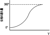
- FIG. 1 is a diagram conceptually illustrating an example of a liquid crystal orientation pattern in a radio wave control element. 1 is a diagram showing the relationship between the applied voltage and the amount of phase delay of a radio wave.
- FIG. 13 is a diagram conceptually illustrating another example of a radio wave control element.
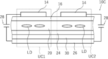
- FIG. 13 is a diagram conceptually illustrating another example of a radio wave control element.
- FIG. 13 is a diagram conceptually illustrating another example of a radio wave control element.
- FIG. 13 is a diagram conceptually illustrating another example of a radio wave control element.
- FIG. 13 is a
- parallel and orthogonal do not mean parallel and orthogonal in the strict sense, but rather mean a range of parallel ⁇ 5° and orthogonal ⁇ 5°, respectively.
- each component may be a single substance corresponding to the component, or two or more substances may be used in combination.
- the content of that component refers to the total content of the substances used in combination, unless otherwise specified.
- the bond direction of the divalent group is not limited unless otherwise specified.
- the compound when Y is -CO-O- in a compound represented by the formula "X-Y-Z", the compound may be either "X-O-CO-Z" or "X-CO-O-Z".
- the liquid crystal composition for radio wave control element of the present invention (hereinafter also simply referred to as “the composition”) contains at least one dichroic dye, the total content of the dichroic dye being 30 mass % or more relative to the total mass of the liquid crystal composition for radio wave control element, and the integrated absorbance Q, expressed by the formula (1) described below, in the wavelength range of 350 to 1000 nm in the absorption spectrum of a chloroform solution of the liquid crystal composition for radio wave control element is 10,000 L g -1 cm -1 or more.
- the integrated absorbance Q which is a characteristic feature of the present composition, will be described in detail below, and then the components contained in the present composition will be described in detail.
- the composition has an absorption spectrum in a chloroform solution having an integrated absorbance Q in the wavelength range of 350 to 1000 nm, which is represented by the formula (1) described below, of 10000 L ⁇ g ⁇ 1 ⁇ cm ⁇ 1 or more.
- the integrated absorbance Q is 10,000 L ⁇ g -1 ⁇ cm -1 or more
- the composition can become a material having a large refractive index anisotropy for radio waves. More specifically, as described below, the refractive index anisotropy for radio waves can be increased by orienting the dichroic dye in the composition.
- radio waves refer to electromagnetic waves with a frequency of 0.007 to 0.3 THz, and have a strong tendency to travel in a straight line due to their high frequency.
- the integrated absorbance Q is an index representing the light absorption characteristics of the present composition in the wavelength range of 350 to 1000 nm, and a high value of this integrated absorbance Q means excellent absorption characteristics. It is known that the refractive index of a substance is related to the light absorption characteristics, and the present inventors have found that by adjusting the integrated absorbance Q of the present composition within a predetermined range, the refractive index anisotropy for radio waves can be significantly increased. In particular, they have found that by increasing the absorption characteristics in the wavelength range of 350 to 1000 nm, the refractive index in the radio wave region can be increased, and as a result, the refractive index anisotropy for radio waves can be increased.
- the integrated absorbance Q is preferably 11,000 L ⁇ g -1 ⁇ cm -1 or more, more preferably 12,000 L ⁇ g- 1 ⁇ cm -1 or more, even more preferably 13,000 L ⁇ g -1 ⁇ cm -1 or more, and particularly preferably 15,000 L ⁇ g -1 ⁇ cm -1 or more.
- the upper limit of the integrated absorbance Q is not particularly limited, but is often 50,000 L ⁇ g ⁇ 1 ⁇ cm ⁇ 1 or less, more often 40,000 L ⁇ g ⁇ 1 ⁇ cm ⁇ 1 or less, and even more often 30,000 L ⁇ g ⁇ 1 ⁇ cm ⁇ 1 or less.
- the cumulative absorbance Q is calculated using the following formula (1):
- Q represents the integrated absorbance (L g -1 cm -1 )
- D represents the mass concentration (g L -1 ) of the liquid crystal composition for radio wave control element in a chloroform solution
- L represents the optical path length (cm) of the cell used to measure the absorption spectrum
- Abs( ⁇ ) represents the absorbance at wavelength ⁇ (nm).
- the definite integral in formula (1) represents the value obtained by numerically integrating the absorbance measured at 1 nm intervals from 350 to 1000 nm.
- the integrated absorbance Q can be measured using a commercially available device, such as a spectrophotometer UV-3100PC manufactured by Shimadzu Corporation.
- the integrated absorbance Q is measured by filling a cell having a predetermined optical path length with a chloroform solution in which a predetermined amount of a liquid crystal composition for a radio wave control element is dissolved.
- a dichroic dye is a substance that exhibits dichroism, and dichroism refers to the property of having different absorbance depending on the direction of polarization.
- the "dichroic dye" in the present invention preferably has a maximum absorption wavelength in the range of 350 to 1000 nm.
- an appropriate and optimal type of dichroic dye is selected so as to satisfy the above-mentioned range of the integrated absorbance Q.
- the dichroic dye may be used alone or in combination of two or more kinds.
- the present composition preferably contains two or more kinds of dichroic dyes.
- the present composition preferably contains 2 to 4 kinds of dichroic dyes, and more preferably contains 2 to 3 kinds of dichroic dyes.
- the dichroic dye preferably exhibits liquid crystallinity, that is, a liquid crystal dichroic dye is preferred.
- exhibiting liquid crystallinity means that the compound has the property of exhibiting a liquid crystal phase (intermediate phase) between a crystalline phase (low temperature side) and an isotropic phase (high temperature side) when the temperature is changed.
- the optical anisotropy and fluidity derived from the liquid crystal phase can be confirmed by observing the compound under a polarizing microscope while heating or lowering the temperature.
- the compound represented by formula (X) is preferred as the dichroic dye, since it provides a more excellent effect of the present invention.
- R 1 and R 2 each independently represent a linear or branched hydrocarbon group having 1 to 10 carbon atoms, and the hydrocarbon group may contain an oxygen atom, a nitrogen atom, or a sulfur atom.
- the hydrocarbon group has 1 to 10 carbon atoms, preferably 1 to 8 carbon atoms, and more preferably 2 to 6 carbon atoms, in that the effects of the present invention are more excellent.
- the hydrocarbon group may be linear or branched, with linear being preferred.
- the hydrocarbon may be a saturated or unsaturated hydrocarbon group.
- the hydrocarbon group may contain an oxygen atom, a nitrogen atom, or a sulfur atom.
- the hydrocarbon group may contain a plurality of atoms selected from the group consisting of oxygen atoms, nitrogen atoms, and sulfur atoms.
- the above-mentioned hydrocarbon group may contain -O-, -S-, -CO-, -CS-, -CO-O-, -CO-NR 10 -, -NR 10 - or a combination thereof between carbon atoms or at the terminal.
- R10 represents a hydrogen atom or an alkyl group.
- the above-mentioned hydrocarbon group is preferably an alkyl group which may contain -O-, -S-, -CO-, -CS-, -CO-O-, -CO-NR 10 -, -NR 10 - or a combination thereof between carbon atoms or at the terminal.
- R 1 and R 2 may be bonded to each other to form a ring.
- the ring formed may be an aliphatic ring or an aromatic ring.
- a and B each independently represent a divalent aromatic ring group.
- the divalent aromatic ring group includes a divalent aromatic hydrocarbon ring group and a divalent aromatic heterocyclic group.
- the divalent aromatic hydrocarbon ring group is a group obtained by removing two hydrogen atoms from an aromatic hydrocarbon ring.
- the aromatic hydrocarbon ring may be a single ring or a condensed ring. Examples of the aromatic hydrocarbon ring include a benzene ring, a naphthalene ring, an anthracene ring, a pyrene ring, a phenanthrene ring, and a fluorene ring.
- a divalent aromatic heterocyclic group is a group formed by removing two hydrogen atoms from an aromatic heterocycle.
- the aromatic heterocycle may be a monocycle or a condensed ring.
- the aromatic heterocycle include a pyridine ring, a pyrimidine ring, a pyridazine ring, a pyrazine ring, a triazine ring (for example, a 1,2,3-triazine ring, a 1,2,4-triazine ring, and a 1,3,5-triazine ring), a tetrazine ring (for example, a 1,2,4,5-tetrazine ring), a quinoxaline ring, a pyrrole ring, a furan ring, a thiophene ring, an imidazole ring, an oxazole ring, a thiazole ring, a benzopyrrole ring, a benzofuran ring, a benzothiophene ring, a benzimidazole ring, a benzoxazole
- thiadiazole ring for example, thieno[2,3-d]thiazole ring, etc.
- benzothiadiazole ring benzodithiophene ring (for example, benzo[1,2-b:4,5-b']dithiophene ring, etc.), thienothiophene ring (for example, thieno[3,2-b]thiophene ring, etc.), thiazolothiazole ring (for example, thiazolo[5,4-d]thiazole ring, etc.), naphthodithiophene ring (for example, naphtho[2,3-b: 6,7-b']dithiophene ring, naphtho[2,1-b:6,5-b']dithiophene ring, naphtho[1,2-b:5,6-b']dithiophene ring, 1,8-dithiadicyclopenta[b,g]naphthal
- Each R independently represents a hydrogen atom, a halogen atom, or an alkyl group having 1 to 6 carbon atoms.
- n represents an integer from 1 to 3, and when n is 2 or 3, the multiple As and Ls may be the same or different.
- R3 represents a hydrogen atom or a substituent.
- the type of the substituent is not particularly limited, and examples thereof include halogen atoms (e.g., fluorine atoms, chlorine atoms, bromine atoms, iodine atoms, etc.), hydrocarbon groups (alkyl groups (including cycloalkyl groups, bicycloalkyl groups, and tricycloalkyl groups), alkenyl groups (including cycloalkenyl groups and bicycloalkenyl groups), alkynyl groups, and aryl groups), heterocyclic groups, cyano groups, isothiocyanate groups, nitro groups, alkoxy groups, aryloxy groups, silyl groups, silyloxy groups, heterocyclic oxy groups, acyloxy groups, carbamoyloxy groups, alkoxycarbonyloxy groups, aryloxycarbonyl groups, etc.
- halogen atoms e.g., fluorine atoms, chlorine
- alkyl group examples include an oxy group, a primary, secondary or tertiary amino group (including anilino group), an alkylthio group, an arylthio group, a heterocyclic thio group, an alkyl or arylsulfinyl group, an alkyl or arylsulfonyl group, an acyl group, an aryloxycarbonyl group, an alkoxycarbonyl group, an aryl or heterocyclic azo group, an imido group, a phosphino group, a phosphinyl group, a phosphinyloxy group, a phosphinylamino group, a phosphono group, a carboxy group, a phosphoric acid group, a sulfonic acid group, a hydroxyl group, a thiol group, an acylamino group, a carbamoyl group, a ureido group, a boronic
- the substituent is preferably an alkyl group, an alkoxy group, a cyano group, or an isothiocyanate group, which may contain an oxygen atom, a nitrogen atom, or a sulfur atom.
- the alkyl group may contain an oxygen atom, a nitrogen atom, or a sulfur atom.
- the alkyl group and the alkoxy group may contain -O-, -S-, -CO-, -CS-, -CO-O-, -CO-NR 10 -, -NR 10 -, or a combination thereof between carbon atoms or at the terminal.
- R 10 represents a hydrogen atom or an alkyl group.
- the alkyl group and alkoxy group may contain a plurality of groups selected from the group consisting of --O--, --S--, --CO--, --CS--, --CO--O--, --CO--NR 10 --, --NR 10 --, and combinations thereof.
- the number of carbon atoms in the alkyl group and alkoxy group is not particularly limited, and is preferably 1-30, more preferably 1-25, and even more preferably 3-25.
- the dichroic dye used in the present invention is also preferably a compound represented by formula (Y).
- at least one of R 11 and R 12 represents an alkyl group having an asymmetric carbon atom, and the total number of asymmetric carbon atoms possessed by R 11 and R 12 is 2 or more.
- L 11 and L 12 each independently represent a single bond, —O—, —CO—, —CO—O—, —O—CO—O—, —NR 13 — or —CH ⁇ CH—; may be substituted with S.
- R 13 represents an alkyl group which may have a substituent.
- a 11 and B 11 each independently represent an aromatic ring group which may have a substituent or an aliphatic ring group which may have a substituent. Examples of the aromatic ring group represented by A 11 and B 11 include the same divalent aromatic hydrocarbon ring group or divalent aromatic heterocyclic group as described for A and B in formula (X). When a plurality of B 11 are present, the B 11 may be the same or different.
- Z 11 represents a single bond, —O—, —CO—, —CO—O—, —O—CO—O—, —CR Z ⁇ CR Z —, —C ⁇ C—, —N ⁇ N—, — CR Z ⁇ CR Z -CR Z ⁇ CR Z -, -C ⁇ C-C ⁇ C-, -CR Z ⁇ CR Z -CO-, or -CR Z ⁇ CR Z -CO-O-, O is , and when a plurality of Z 11 are present, the Z 11 may be the same or different.
- R and Z each independently represent a hydrogen atom or a fluorine atom.
- m represents an integer of 1 to 4.
- the dichroic dyes used in the present invention may be the compounds described in "Dichroic Dyes for Liquid Crystal Display” (A.V. Ivashchenko, CRC, 1994). Methine dyes such as cyanine, oxonol, and merocyanine may also be used.
- the total content of the dichroic dye in the composition is 30% by mass or more based on the total mass of the composition.
- the total content of the dichroic dye refers to the content of the one dichroic dye relative to the total mass of the composition.
- the total content of the dichroic dye refers to the total amount of the two or more dichroic dyes.
- a liquid crystal composition layer made of the present composition can have a state in which the refractive index anisotropy for radio waves is large.
- the total content of the dichroic dyes in the composition is preferably 50% by mass or more, more preferably 80% by mass or more, and even more preferably 90% by mass or more, based on the total mass of the composition.
- the upper limit is not particularly limited, but may be 100% by mass or less.
- the present composition may contain other components in addition to the dichroic dye.
- the other components include, for example, liquid crystal compounds.
- the liquid crystal compound that may be used in combination with the dichroic dye is preferably a liquid crystal compound having a skeleton with a high ⁇ n.
- Examples of the skeleton with a high ⁇ n include a skeleton having multiple rings selected from aromatic hydrocarbon rings and aromatic heterocycles, and having a triple bond and/or a double bond as a linking group.
- the linking group is preferably tolane, ditolane, vinylene, or butadiene, and one molecule may have multiple of these linking groups.
- the liquid crystal compound preferably has an electron-donating or electron-accepting substituent at the terminal.
- Examples of the electron-donating substituent include an alkoxy group, a thioalkoxy group, and an alkylamino group.
- Examples of the electron-accepting group include a cyano group, a nitro group, an isocyanate group, an isothiocyanate group, a cyanovinylene group, and a dicyanovinylene group. These compounds do not need to be visible-transparent, and the longer the absorption wavelength is, the higher the ⁇ n tends to be.
- the maximum absorption wavelength ( ⁇ max) of these compounds is preferably 320 nm or more, more preferably 350 nm or more, and even more preferably 380 nm or more.
- the composition is preferably substantially free of a solvent, meaning that the content of the solvent is 5% by mass or less, and preferably 1% by mass or less, based on the total mass of the composition.
- the present composition is a composition that exhibits liquid crystallinity.
- the present composition contains a liquid crystal dichroic dye, the present composition can exhibit liquid crystallinity.
- the composition can be applied to a radio wave control element.
- the radio wave control element acts on radio waves. Examples of radio waves include radio waves with a frequency of 0.007 to 0.3 THz. Radio waves in this frequency band RW are also called high-frequency radio waves (centimeter waves, millimeter waves, terahertz waves), and are capable of high-capacity wireless communication while also having high linearity.
- radio wave control element is a radio wave control element having, in this order, a first electrode, a liquid crystal composition layer made of the present composition, and a second electrode.
- a voltage is applied between the first electrode and the second electrode to control the orientation state of the dichroic dye contained in the liquid crystal composition layer, thereby adjusting the refractive index anisotropy of the liquid crystal composition layer, thereby adjusting the propagation direction of radio waves.
- the alignment state of the dichroic dye can be changed by voltage application. In particular, when the dichroic dye exhibits liquid crystallinity, the above-mentioned characteristics are easily exhibited.
- a state exhibiting large refractive index anisotropy can be achieved by controlling the orientation state of the dichroic dye.
- the response speed depends on the film thickness of the liquid crystal composition layer. Since a liquid crystal composition layer made of this composition can exhibit a state exhibiting large refractive index anisotropy, the film thickness of the liquid crystal composition layer can be made thin, and as a result, the response speed can be improved. Therefore, the reflection direction of the incident radio wave can be switched in a short time.
- the above-mentioned integrated absorbance Q is equal to or greater than a predetermined value, which can reduce the noise of a sensor using visible light or infrared light. More specifically, if the integrated absorbance Q is large, the visible light or infrared light that hits the radio wave control element is absorbed by the liquid crystal composition layer and does not become noise light, resulting in a radio wave control element that is less likely to cause noise light. In other words, an electromagnetic wave control element that does not cause unnecessary reflection and scattering by the radio wave control element and is less likely to cause noise in signal detection by a visible light and infrared light sensor shared with an antenna can be realized. Also, from the viewpoint of decoration, it is desirable because it has the effect of making the electrodes used in the radio wave control element less visible.
- a radio wave control element 10A according to the technology of the present disclosure is used in the radio wave reflecting device 2 shown in Fig. 1.
- the radio wave reflecting device 2 is capable of reflecting radio waves RW, which have a high degree of directional propagating property and are radiated from an antenna ANT arranged behind a building BL, toward an area AR1 in front of the building BL, which is in the shadow when viewed from the antenna ANT. Furthermore, the radio wave reflecting device 2 can change the reflection direction of the radio wave RW to different directions between the multiple areas AR1 and AR2.
- the radio wave reflecting device 2 can change the area to which the radio wave RW is supplied by changing the reflection direction of the radio wave RW depending on the time of day.
- the radio wave control element 10A has a metasurface structure 12 and is a reflective radio wave control element that reflects the traveling direction of the radio wave RW in a desired direction.
- the metasurface structure 12 is a structure that uses a metamaterial.
- a metamaterial is an artificial material that exhibits characteristics not found in natural materials, such as a negative refractive index for radio waves.
- the radio wave control element 10A is configured such that a plurality of unit cells UC are arranged two-dimensionally, and a two-dimensional plane formed by the arrangement of the plurality of unit cells UC becomes a reflection surface for the radio wave RW.
- Each unit cell UC includes a microstructure 14 as a metamaterial, and constitutes a minimum unit that can actively change the phase of the radio wave RW on the reflection surface.
- the microstructure 14 is made of metal, for example.
- the size of the microstructure 14 is on the order of the wavelength of the incident radio wave RW or less, and functions as a resonator that resonates by interacting with the incident radio wave RW.
- the microstructure 14 can be considered electrically equivalent to a resonant circuit in which, for example, a coil and a capacitor are connected in series to resonate an alternating current.
- the phase of the incident radio wave RW changes due to the resonant action of the microstructure 14.
- the radio wave control element 10A acts mainly on radio waves RW having frequencies between 0.007 and 0.3 THz.
- the metasurface structure 12 is configured to act on radio waves RW with a frequency of 0.007 to 0.3 THz.
- the wavelength of radio waves RW with a frequency of 0.007 to 0.3 THz is 0.07 to 3 mm, and the size of the microstructures 14 constituting the metasurface structure 12 is, for example, on the order of about 1/2 the wavelength.
- the microstructures 14 resonate with the radio waves RW passing through them, and function as a phase modulation element that modulates the phase of the radio waves RW.
- the overall traveling direction of the radio wave RW can be considered as the normal direction to the straight line connecting the wavefronts of the multiple radio waves RW.
- the amount of phase delay of the radio wave RW that is incident on and reflected from each of the multiple unit cells UC arranged in one dimension is considered to be gradually increased from the unit cell UC on the right to the unit cell UC on the left. In this way, even if the straight line connecting the wavefronts of each incident radio wave RW is parallel to the reflecting surface, the straight line connecting the wavefronts of each radio wave RW reflected by each unit cell UC is inclined with respect to the reflecting surface.
- the outgoing direction OUT which is the traveling direction of the radio wave RW that is emitted from the reflecting surface, changes by an angle ⁇ with respect to the incident direction IN of the radio wave RW.
- the traveling direction of the radio wave RW can be controlled by performing phase modulation, i.e., controlling the amount of phase delay, for each unit cell UC.
- the radio wave reflecting device 2 can change the direction of propagation of the radio wave RW in a direction other than specular reflection by using the metasurface structure 12.
- the radio wave reflecting device 2 can change the direction of propagation of the radio wave RW in a direction other than specular reflection by using the metasurface structure 12.
- the amount of phase delay in each unit cell UC it is possible to actively change the direction of propagation of the radio wave RW.
- the radio wave control element 10A uses a liquid crystal composition layer 20 as an element that actively changes the resonance conditions of the microstructure 14 of the metasurface structure 12.
- the radio wave control element 10A has a first electrode layer 26, a liquid crystal composition layer 20, and a metasurface structure 12, in that order.
- the liquid crystal composition layer 20 is provided on a support 24.
- the first electrode layer 26 is provided to entirely cover the surface of the support 24 opposite the liquid crystal composition layer 20.
- the liquid crystal composition layer 20 contains a dichroic dye (liquid crystal dichroic dye LD) that exhibits liquid crystallinity.
- Each unit cell UC is composed of a microstructure 14, a liquid crystal composition layer 20, and a first electrode layer 26.
- the microstructure 14 is provided individually for each unit cell UC.
- the remaining components, the support 16, the liquid crystal composition layer 20, the support 24, and the first electrode layer 26, are not independent components for each unit cell UC, but are integrally formed in regions corresponding to multiple unit cells UC.
- the first electrode layer 26 and the support 24, and the liquid crystal composition layer 20 and the support 16 are attached using an adhesive (adhesive or adhesive) as necessary.
- an adhesive adhesive or adhesive
- OCA Optical Clear Adhesive
- the microstructure 14 is formed, for example, from a conductive material, and serves as an electrode that constitutes an electrode pair together with the first electrode layer 26 . Further, a power source 28 for applying a voltage between the microstructure 14 and the first electrode layer 26 is connected to each microstructure 14. Therefore, it is possible to control the magnitude of the voltage applied to each unit cell UC.
- the first electrode layer 26 is a common electrode common to each unit cell UC, and the microstructure 14 of each unit cell UC functions as an individual electrode.
- the first electrode layer 26 functioning as a common electrode is an example of a "first electrode" according to the technology of the present disclosure, and the individual electrode shared by the microstructure 14 is an example of a "second electrode".
- the microstructure 14 as the second electrode and the first electrode layer 26 as the first electrode are an example of an "electrode pair for applying a voltage".
- the radio wave control element 10A is a reflective type, and the first electrode layer 26 also serves as a reflective layer that reflects the radio wave RW.
- the orientation state (hereinafter also referred to as the orientation pattern) of the liquid crystal dichroic dye changes due to the application of a voltage.
- the alignment direction of the microstructures 14 of each unit cell UC is a direction (X direction or Y direction in the figure) perpendicular to the thickness direction of the liquid crystal composition layer 20 (Z direction in the figure).
- the microstructures 14 and the first electrode layer 26 are arranged on both sides of the thickness direction of the liquid crystal composition layer 20.
- the application of the voltage generates an electric field in the thickness direction of the liquid crystal composition layer 20, and the orientation state of the liquid crystal dichroic dye LD of each unit cell UC changes.
- the orientation state of the liquid crystal dichroic dye LD of each unit cell UC can be adjusted by adjusting the voltage applied to each unit cell UC.
- the liquid crystal dichroic dye LD has a cross section that is approximately elliptical with a major axis and a minor axis.
- the liquid crystal dichroic dye LD is oriented with its major axis along the thickness direction of the liquid crystal composition layer 20. In the following explanation, this alignment state is also referred to as "vertical alignment".
- the orientation state of the liquid crystal dichroic dye LD changes.
- the orientation state of the liquid crystal dichroic dye LD in the region corresponding to the microstructure 14 changes depending on the magnitude of the applied voltage, and tilts with respect to the thickness direction of the liquid crystal composition layer 20.
- the liquid crystal dichroic dye LD has a maximum tilt angle.
- the liquid crystal dichroic dye LD When the tilt angle is maximum, the liquid crystal dichroic dye LD is oriented in such a way that the major axis is aligned along a direction perpendicular to the thickness direction of the liquid crystal composition layer 20.
- the orientation state with the maximum tilt angle is also referred to as "horizontal orientation”.
- the refractive index of the liquid crystal composition layer 20 is greater as the inclination of the liquid crystal dichroic dye LD increases, i.e., the angle of the long axis of the liquid crystal dichroic dye LD is closer to the main surface direction of the liquid crystal composition layer 20 (X direction or Y direction in FIG. 5). Conversely, the refractive index of the liquid crystal composition layer 20 is smaller as the inclination of the liquid crystal dichroic dye LD decreases, i.e., the angle of the long axis of the liquid crystal dichroic dye LD is closer to the thickness direction of the liquid crystal composition layer 20 (Z direction in the figure).
- Such a change in the refractive index of the liquid crystal composition layer 20 of each unit cell UC changes the resonance condition of the microstructure 14, and the amount of phase delay of the incident radio wave RW changes.
- the amount of phase delay of the unit cell UC in the lower row of FIG. 5 is greater than that of the unit cell UC in the upper row of FIG. 5.
- the refractive index of the liquid crystal composition layer 20 changes with respect to the radio wave RW passing through each unit cell UC. Since the refractive index and the dielectric constant are positively correlated, the change in the refractive index of the liquid crystal composition layer 20 changes the resonance condition of the microstructure 14 functioning as a resonator. The change in the resonance condition of the microstructure 14 appears as a change in the amount of phase delay of the radio wave RW. Therefore, by changing the refractive index of the liquid crystal composition layer 20, the amount of phase delay of the radio wave RW can be changed.
- the change in the refractive index of the liquid crystal composition layer 20 itself causes a change in the amount of phase delay of the radio wave RW. Since the refractive index of the liquid crystal composition layer 20 of each unit cell UC changes depending on the voltage V applied to each unit cell UC, the relationship between the voltage V and the amount of phase delay of the radio wave RW is, for example, as shown in FIG. 6.
- the radio wave RW when the radio wave RW is incident on the radio wave control element 10A from the microstructure 14 side, the radio wave RW passes through the microstructure 14 and the liquid crystal composition layer 20 in this order. Furthermore, the radio wave RW is reflected by the first electrode layer 26, which also serves as a reflective layer, and passes through the liquid crystal composition layer 20 and the microstructure 14 again in this order, and is emitted from the radio wave control element 10A. The radio wave RW is reflected through such an input/output path. In the input/output path, the radio wave RW passing through each unit cell UC is phase-modulated by resonance with the microstructure 14, and phase-modulated by passing through the liquid crystal composition layer 20.
- the resonance condition of the microstructure 14 is determined according to the refractive index of the liquid crystal composition layer 20, and phase modulation of the radio wave RW occurs due to resonance according to the condition.
- phase modulation of the radio wave RW also occurs according to the magnitude of the refractive index of the liquid crystal composition layer 20.
- the reflection direction of the radio wave RW reflected by the radio wave control element 10A is controlled by controlling the amount of phase delay of the radio wave RW for each unit cell UC through the applied voltage V.
- a normal reflector can only change the direction of propagation of the radio wave RW in the direction of specular reflection, but the radio wave control element 10A uses the metasurface structure 12, making it possible to change the direction of propagation of the radio wave RW in a direction other than specular reflection.
- the radio wave control element 10A uses the metasurface structure 12, making it possible to change the direction of propagation of the radio wave RW in a direction other than specular reflection.
- by actively changing the amount of phase delay in each unit cell UC it is possible to actively change the direction of propagation of the radio wave RW.
- the radio wave RW emitted from the radio wave control element 10A may be made to converge toward a single focal point, or conversely, may be made to diverge.
- the direction of travel of the emitted radio wave RW can be controlled by adjusting the voltage applied to each unit cell UC, thereby adjusting the amount of phase delay of the radio wave RW for each unit cell UC.
- the metasurface structure 12 like known metasurface structures, is formed by two-dimensionally arranging microstructures 14, which are metamaterials, on a support 16.
- the microstructures 14 are two-dimensionally arranged at equal intervals in the X and Y directions that are perpendicular to each other.
- all of the microstructures 14 are the same.
- the support 16 there are no limitations on the support 16, and any known sheet-like material can be used as long as it can support the microstructure 14 and can transmit radio waves RW of 0.007 to 0.3 THz, which is the frequency that the radio wave control element 10A targets.
- the support 16 include metal substrates with oxide insulating layers, such as silicon substrates with silicon oxide, supports made of oxides such as silicon oxide, supports made of semiconductors such as germanium and chalcogenide glass, polyacrylic resin films such as polymethyl methacrylate, cellulose resin films such as cellulose triacetate, cycloolefin polymer films (for example, trade name "Arton” manufactured by JSR Corporation, trade name “ZEONOR” manufactured by Nippon Zeon Co., Ltd.), polyethylene terephthalate (PET) films, resin films such as polycarbonate films and polyvinyl chloride films, and glass plates.
- metal substrates with oxide insulating layers such as silicon substrates with silicon oxide, supports made of oxides such as silicon oxide, supports made of semiconductor
- the thickness of the support 16 is set appropriately depending on the material from which the support 16 is made so as to satisfy these conditions.
- the support 16 is not a required component of the metasurface structure 12, and the support 16 may be omitted.
- the metasurface structure 12 may be formed by arranging the microstructures 14 directly on the surface of the liquid crystal composition layer 20.
- the metasurface structure 12 is composed of microstructures 14, which are metamaterials, spaced apart and arranged two-dimensionally on a plane. More specifically, it is composed of an arrangement of unit cells UC, each of which basically consists of one microstructure 14 and the space surrounding the microstructure 14.
- the form of the metasurface structure is basically the same as that of a known metasurface structure. Therefore, in the radio wave control element 10A according to the technology of the present disclosure, various known metasurface structures can be used. That is, in the technology of the present disclosure, there are no limitations on the shape and material of the microstructures 14, the arrangement of the microstructures 14, and the pitch, which is the interval between the microstructures 14.
- the metasurface structure 12 may be designed by a known method according to the wavelength of the radio wave RW to be controlled by the radio wave control element 10A and the target reflection characteristics (for example, the range of controllable reflection directions).
- the amplitude and phase of the radio wave RW reflected by the microstructures 14 used may be calculated using commercially available simulation software, and the arrangement of the microstructures 14 may be set so as to obtain the desired distribution of phase modulation amount.
- phase modulation occurs due to the refractive index and further the interaction between the refractive index and the microstructures 14, and the phase modulation amount is determined by the resonance characteristics of the microstructures 14, which change depending on the refractive index.
- the radio wave control element 10A is intended to control radio waves RW with a frequency of 0.007 to 0.3 THz. Therefore, the microstructures 14 of the metasurface structure 12 are selected so as to provide a desired phase difference to the radio waves RW of this frequency, and the arrangement of the microstructures is set. Specifically, when radio waves RW with a frequency of 0.007 to 0.3 THz are to be controlled, the wavelength range of the radio waves RW is approximately 0.07 to 3 mm, so the size of the microstructures 14 is selected to be within that wavelength range.
- the number of microstructures 14 that one unit cell UC has is basically one, but the technology of the present disclosure is not limited to this. That is, in the radio wave control element according to the technology of the present disclosure, one unit cell UC may have multiple microstructures 14 as necessary depending on the reflection characteristics, the size, material and shape of the microstructures 14, and the size of the unit cell UC. In this case, one unit cell UC may have different microstructures 14. However, because the unit cell UC is the smallest unit capable of actively changing the phase of the radio wave RW, even when one unit cell UC has multiple microstructures 14, the amount of phase modulation is determined for each unit cell UC.
- microstructure 14 there is no limitation on the material for forming the microstructure 14, and various materials used as microstructures in known metasurface structures can be used.
- materials for forming the microstructure 14 include metals and dielectrics. In the case of metals, copper, gold, and silver are preferred examples because of their low optical loss.
- composites consisting of metal particles and binders, and oxide semiconductors can also be used as materials for forming the microstructure 14.
- dielectrics silicon, titanium oxide, and germanium are preferred examples because they have a large refractive index and can increase the amount of phase modulation. Note that, as shown in FIG. 4, when the microstructure 14 also serves as an electrode that forms an electrode pair with the first electrode layer 26, the microstructure 14 is formed of a conductor.
- microstructure 14 there are no limitations on the shape of the microstructure 14, and various shapes used as microstructures in known metasurface structures can be used. Examples include a cross-shaped solid like a cross of rectangular parallelepipeds, a rectangular parallelepiped shape, a cylindrical shape, a V-shaped solid like a rectangular parallelepiped connected at its ends as shown in JP 2018-046395 A, an approximately H-shaped solid like an H-beam, and an approximately C-shaped solid like a C-channel. As shown in JP 2018-046395 A, various shapes can be used for the V-shaped solid and the cross-shaped solid by adjusting the angle between the two rectangular parallelepipeds. In addition, a solid having a bottom shape as shown in Figure 5 of "Appl. Sci. 2018, 8(9), 1689; https://doi.org/10.3390/app8091689" can also be used.
- microstructures 14 may be of the same type, or multiple types may be used in combination. Furthermore, the same microstructures 14 may be arranged in the same orientation in the XY plane, or in different orientations. Furthermore, microstructures 14 of the same orientation and those of different orientations may be mixed. However, in the radio wave control element 10A according to the technology disclosed herein, it is preferable to use only one type of microstructure 14 and to arrange all of the microstructures 14 in the same orientation.
- the metasurface structure 12 is preferably configured such that the same microstructures 14, all of which have the same structure, are arranged two-dimensionally at equal intervals in the mutually orthogonal X and Y directions.
- the technology disclosed herein is not limited to this, and multiple types of microstructures may be used in combination as described above, and the arrangement intervals and arrangement of the microstructures 14 may also differ in the surface direction of the support 16.
- the metasurface structure 12 uses all the same microstructures 14.
- the microstructures 14 in the metasurface structure 12 are spaced at equal intervals, and it is even more preferable that they are spaced at equal intervals in both the orthogonal X and Y directions.
- the liquid crystal composition layer 20 is a layer in which the liquid crystal dichroic dye LD is aligned in a preset state, and as described above, the alignment state of the liquid crystal dichroic dye LD changes when a voltage is applied.
- the liquid crystal dichroic dye LD when no voltage is applied, the liquid crystal dichroic dye LD is vertically aligned. When a voltage is applied to the liquid crystal composition layer 20, the liquid crystal dichroic dye LD is aligned at an angle relative to the thickness direction in response to the voltage, and is aligned at a maximum horizontally.
- the alignment of the liquid crystal dichroic dye LD is not limited to changing from a vertical alignment to a horizontal alignment or vice versa, and may change from an inclined state relative to the thickness direction to a horizontal or vertical alignment, may change from a horizontal or vertical alignment to an inclined state relative to the thickness direction, or may change at an angle from an inclined state relative to the thickness direction to an inclined state relative to the thickness direction.
- the liquid crystal composition layer 20 may be formed, for example, on the surface of an alignment film to be described later by a known method.
- the liquid crystal composition layer 20 is formed on a support 24.
- the support 24 is basically the same as the support 16 described above.
- the support 24 on which the liquid crystal composition layer 20 is formed may further have an alignment film for aligning the liquid crystal dichroic dye LD in a predetermined state on the surface of the main body on which the liquid crystal composition layer 20 is formed, with the support 16 described above as the main body.
- Various known alignment films can be used.
- Examples include a rubbed film made of an organic compound such as a polymer, an obliquely evaporated film of an inorganic compound, a film with microgrooves, and a film in which LB (Langmuir-Blodgett) films of organic compounds such as ⁇ -tricosanoic acid, dioctadecylmethylammonium chloride, and methyl stearyl acid are accumulated by the Langmuir-Blodgett method.
- LB Lightmuir-Blodgett films of organic compounds such as ⁇ -tricosanoic acid, dioctadecylmethylammonium chloride, and methyl stearyl acid are accumulated by the Langmuir-Blodgett method.
- so-called photo-alignment films which are formed by irradiating a photo-alignable material with polarized or non-polarized light, can also be used as the alignment film. These
- the surface of the support 24 that forms the liquid crystal composition layer 20, opposite the liquid crystal composition layer 20, is entirely covered with a first electrode layer 26.
- the first electrode layer 26 is an electrode that changes the orientation of the liquid crystal dichroic dye LD in the liquid crystal composition layer 20, and also acts as a reflective layer that reflects radio waves RW with a frequency of 0.007 to 0.3 THz that are incident from the metasurface structure 12 side, as described above.
- the first electrode layer 26 there are no limitations on the first electrode layer 26, and any sheet-like material made of various known materials can be used as long as it has sufficient conductivity and is capable of reflecting radio waves RW.
- the first electrode layer 26 include a metal layer such as copper, aluminum, gold, or silver, an inorganic conductive material such as ITO (tin-doped indium oxide), an organic conductive material such as polythiophene represented by PEDOT (poly 3,4-ethylenedioxythiophene), and graphene.
- ITO in-doped indium oxide
- PEDOT poly 3,4-ethylenedioxythiophene
- graphene graphene.
- Inorganic conductive materials, organic conductive materials, and graphene are transparent to visible light, but act as a reflective layer for radio waves of the above frequencies.
- the thickness of the first electrode layer 26 can be set appropriately depending on the material from which the first electrode layer 26 is formed so that the target radio waves can be reflected with the required reflectance.
- the radio wave control element 10A is a reflective radio wave control element having a metasurface structure 12 and a liquid crystal composition layer 20.
- power is supplied to each microstructure 14 to change the orientation state of the liquid crystal dichroic dye LD in the corresponding region of the liquid crystal composition layer 20, thereby forming regions with different refractive indices for each unit cell UC, thereby reflecting the radio wave RW in the desired direction.
- the power supplied to each microstructure 14, i.e., the voltage applied to the liquid crystal composition layer 20 the reflection direction of the incident radio wave RW can be switched.
- the refractive index anisotropy ⁇ n of the liquid crystal composition layer 20 with respect to radio waves is not limited, but is preferably large.
- the refractive index anisotropy ⁇ n of the liquid crystal composition layer 20 with respect to radio waves of 100 GHz is preferably 0.35 or more.
- the thickness of the liquid crystal composition layer 20 is made of the present composition containing a predetermined amount of dichroic dye, so that the liquid crystal composition layer 20 can be made thin.
- the thickness of the liquid crystal composition layer 20 is preferably 200 ⁇ m or less, more preferably 150 ⁇ m or less, and even more preferably 100 ⁇ m or less.
- the radio wave control element 10B shown in Fig. 7 has, from the bottom in the figure, a first electrode layer 26, a liquid crystal composition layer 20, and a metasurface structure 12, in this order.
- the liquid crystal composition layer 20 is provided on a support 24.
- the first electrode layer 26 is provided so as to entirely cover the surface of the support 24 opposite to the liquid crystal composition layer 20.
- a temperature adjustment member 30 is provided between the support 24 and the first electrode layer 26.
- the liquid crystal dichroic dye LD when no voltage is applied, the liquid crystal dichroic dye LD is horizontally aligned, and when the applied voltage is increased, the liquid crystal dichroic dye LD is aligned in a vertical direction.
- the temperature adjustment member 30 may also have a heating device that increases the temperature of the liquid crystal composition layer 20, and a cooling device that decreases the temperature of the liquid crystal composition layer 20.
- the procedure for fixing the alignment state of the liquid crystal dichroic dye LD in the liquid crystal composition layer 20 using the radio wave control element 10B is as follows.
- the liquid crystal dichroic dye LD contained in the liquid crystal composition layer 20 a compound that exhibits liquid crystallinity when subjected to a heat treatment by the temperature adjustment member 30 is used.
- the present composition that exhibits a nematic phase at any temperature between 50 and 150° C. and a glassy state or a smectic phase at any temperature below 50° C., as described above.
- the liquid crystal composition layer 20 is heated by the temperature adjustment member 30, and transitioned to a liquid crystal phase.
- a voltage is applied between the first electrode layer 26 and the microstructure 14 to control the alignment direction of the liquid crystal dichroic dye LD.
- the voltages applied to the first unit cell UC1 and the second unit cell UC2 may be changed to make the alignment state of the liquid crystal dichroic dye LD different.
- the temperature falls below the transition temperature of the liquid crystal phase, and the alignment state of the liquid crystal dichroic dye in the state shown in FIG. 8 is fixed. In other words, the alignment state of the liquid crystal dichroic dye can be maintained even without applying a voltage.
- a state with higher alignment can be created depending on the type of dichroic dye used.
- the higher order liquid crystal phase can be fixed by rapidly cooling the radio wave control element.
- the radio wave control element 10C shown in Fig. 9 has the same configuration as the radio wave control element 10B shown in Fig. 7.
- the liquid crystal dichroic dye LD exhibits a nematic phase as well as a smectic phase.
- the liquid crystal dichroic dye LD is horizontally aligned when no voltage is applied, and as the applied voltage is increased, the liquid crystal dichroic dye LD is aligned in a direction that vertically aligns.
- the liquid crystal composition layer 20 is heated by the temperature adjusting member 30 as shown in Fig. 9, and the liquid crystal dichroic dye LD is aligned to produce a nematic phase.
- Fig. 9 corresponds to a mode in which no voltage is applied between the first electrode layer 26 and the microstructure 14, and the liquid crystal dichroic dye LD is aligned horizontally. As shown in Fig.
- the liquid crystal dichroic dye LD is aligned horizontally, the degree of alignment of the nematic phase itself is not high, so that the alignment direction of the liquid crystal dichroic dye LD is partially disturbed.
- the heating treatment of the temperature adjusting member 30 is stopped, and the liquid crystal composition layer 20 is rapidly cooled, whereby the liquid crystal dichroic dye LD can be fixed in a state exhibiting a smectic phase.
- the alignment of the liquid crystal dichroic dye LD is further improved. In other words, by carrying out the rapid cooling treatment, the liquid crystal dichroic dye can be fixed in a state with a higher degree of alignment.
- the radio wave control element may have a layer between the first electrode and the second electrode, the refractive index of which does not change with voltage, or may have a gap between one of the first electrode and the second electrode and the liquid crystal composition layer.
- the radio wave control element 10D shown in FIG. 11 has, from the bottom in the figure, a first electrode layer 26, a dielectric layer 32, a liquid crystal composition layer 20, and a metasurface structure 12, in this order.
- the radio wave control element 10D shown in Fig. 11 has the same configuration as the radio wave control element 10A shown in Fig. 4, except that it has a dielectric layer 32.
- the liquid crystal dichroic dye LD is horizontally aligned when no voltage is applied, and as the applied voltage is increased, the liquid crystal dichroic dye LD is aligned in a direction such that it is vertically aligned.
- the dielectric layer 32 is a layer whose refractive index does not change when a voltage is applied.
- the material constituting the dielectric layer 32 is not particularly limited as long as it has sufficient transparency to the radio waves RW. Examples include semiconductors such as silicon, silicon oxide, germanium, and chalcogenide glass, polyacrylic resins such as polymethyl methacrylate, cellulose resins such as cellulose triacetate, resins such as cycloolefin polymers, polyethylene terephthalate (PET), polycarbonate, and polyvinyl chloride, and glass.
- the dielectric layer 32 may be an alignment film for aligning the above-mentioned liquid crystal dichroic dye LD in a predetermined state.
- the thickness of the dielectric layer 32 is not particularly limited, but is preferably approximately the same as that of the liquid crystal composition layer 20.
- the difference between the thickness of the dielectric layer 32 and the thickness of the liquid crystal composition layer 20 is preferably 100 ⁇ m or less, more preferably 50 ⁇ m or less.
- the location of the driving electrode for applying a voltage to the liquid crystal composition layer is not particularly limited, but the electrode may be the first electrode layer 26 and the microstructure 14. Also, an electrode may be provided between the dielectric layer 32 and the liquid crystal composition layer in order to efficiently apply a voltage to the liquid crystal composition layer. In this case, a high-resistance electrode may be used so as to have little effect on radio waves.
- the electrodes may be positioned so as to sandwich the liquid crystal composition layer in the horizontal direction in order to drive the device with a transverse electric field.
- the dielectric constant of the material constituting the dielectric layer 32 with respect to the applied voltage is not particularly limited.
- the dielectric layer and the dielectric layer are arranged in series between the opposing planar electrodes, such as when the first electrode layer 26 and the microstructure 14 of the radio wave control element 10D are electrodes, it is preferable that the dielectric layer has a high dielectric constant because the electric field to the liquid crystal composition layer can be efficiently increased.
- the dielectric layer has a low dielectric constant because the electric field to the liquid crystal composition layer can be efficiently increased.
- the dielectric layer may be patterned in the in-plane direction or the thickness direction, and the amount of radio wave control can be adjusted by adjusting the in-plane average effective value of the refractive index or the effective value distribution in the element.
- the radio wave control element may also have a light shielding layer that blocks at least a part of light in the wavelength range of 250 to 1000 nm.
- the position of the light-shielding layer in the radio wave control element is not particularly limited, but it is preferably disposed on the side where external light is incident on the liquid crystal composition layer.
- dichroic dyes As dichroic dyes, the following compounds 1-1 to 1-7 and 2-1 to 2-6 were prepared.
- liquid crystal compound A liquid crystal A (RDP-94990 manufactured by DIC Corporation) were prepared as liquid crystal compounds for use in the examples and comparative examples.
- Table 1 shows the integrated absorbance Q of the above compounds 1-1 to 1-7, 2-1 to 2-6, 3, and liquid crystal A, which was measured in the same manner as the integrated absorbance Q of the present composition.
- the integrated absorbance Q of the above compounds 1-1 to 1-7, 2-1 to 2-6, 3, and liquid crystal A was measured in the same manner as the integrated absorbance Q of the present composition, except that D in the above formula (1) is changed to the mass concentration (g ⁇ L ⁇ 1 ) of any of the above compounds 1-1 to 1-7, 2-1 to 2-6, 3, and liquid crystal A in a chloroform solution.
- compositions in which the difference (TB-TA) between the transition temperature (TA) from the crystalline phase to the nematic phase (liquid crystal phase) and the transition temperature (TB) from the nematic phase (liquid crystal phase) to the isotropic phase was 50°C or more were rated as A, those in which the difference (TB-TA) was less than 50°C were rated as B, and those that did not exhibit a liquid crystal phase were rated as C.
- the refractive index anisotropy ⁇ n at radio waves of 100 GHz and 30 GHz was measured by the method disclosed in Applied Optics, Vol. 44, No. 7, p. 1150 (2005).
- the refractive index anisotropy ⁇ n (100 GHz) was measured by filling the above composition in a variable short-circuited waveguide and arranging the dichroic dye in the composition. Radio waves of 100 GHz were input into the waveguide, and the amplitude ratio of the reflected wave to the incident wave was measured. Measurements were performed by changing the direction of the static magnetic field and the length of the short-circuiting tube, and the refractive indexes ne and no were determined.
- the refractive index anisotropy ( ⁇ n (100 GHz)) was calculated from ne-no. Those with ⁇ n (100 GHz) z of 0.4 or more were classified as A, those with ⁇ n (100 GHz) z of 0.35 or more and less than 0.4 were classified as B, and those with less than 0.35 were classified as C. Similarly, for the refractive index anisotropy ⁇ n (30 GHz) measured with an input radio wave of 30 GHz, those with ⁇ n (30 GHz) of 0.4 or more were classified as A, those with ⁇ n (30 GHz) of 0.35 or more and less than 0.4 were classified as B, and those with less than 0.35 were classified as C.
Landscapes
- Chemical & Material Sciences (AREA)
- Physics & Mathematics (AREA)
- Electromagnetism (AREA)
- Crystallography & Structural Chemistry (AREA)
- Engineering & Computer Science (AREA)
- Materials Engineering (AREA)
- Organic Chemistry (AREA)
- Liquid Crystal (AREA)
Priority Applications (2)
| Application Number | Priority Date | Filing Date | Title |
|---|---|---|---|
| JP2025522370A JPWO2024242035A1 (https=) | 2023-05-19 | 2024-05-17 | |
| CN202480033355.2A CN121152860A (zh) | 2023-05-19 | 2024-05-17 | 电波控制元件用液晶组合物、电波控制元件 |
Applications Claiming Priority (2)
| Application Number | Priority Date | Filing Date | Title |
|---|---|---|---|
| JP2023083296 | 2023-05-19 | ||
| JP2023-083296 | 2023-05-19 |
Publications (1)
| Publication Number | Publication Date |
|---|---|
| WO2024242035A1 true WO2024242035A1 (ja) | 2024-11-28 |
Family
ID=93589375
Family Applications (1)
| Application Number | Title | Priority Date | Filing Date |
|---|---|---|---|
| PCT/JP2024/018254 Ceased WO2024242035A1 (ja) | 2023-05-19 | 2024-05-17 | 電波制御素子用液晶組成物、電波制御素子 |
Country Status (3)
| Country | Link |
|---|---|
| JP (1) | JPWO2024242035A1 (https=) |
| CN (1) | CN121152860A (https=) |
| WO (1) | WO2024242035A1 (https=) |
Cited By (2)
| Publication number | Priority date | Publication date | Assignee | Title |
|---|---|---|---|---|
| WO2025204788A1 (ja) * | 2024-03-28 | 2025-10-02 | 富士フイルム株式会社 | 電波制御素子用液晶組成物、電波制御素子、化合物 |
| WO2026023665A1 (ja) * | 2024-07-25 | 2026-01-29 | 富士フイルム株式会社 | 電波制御素子用液晶組成物、電波制御素子 |
Citations (5)
| Publication number | Priority date | Publication date | Assignee | Title |
|---|---|---|---|---|
| JP2018501361A (ja) * | 2014-12-19 | 2018-01-18 | メルク パテント ゲゼルシャフト ミット ベシュレンクテル ハフツングMerck Patent Gesellschaft mit beschraenkter Haftung | 液晶媒体およびそれを含む高周波数素子 |
| JP2019512023A (ja) * | 2016-02-08 | 2019-05-09 | メルク・パテント・ゲゼルシヤフト・ミツト・ベシユレンクテル・ハフツングMerck Patent GmbH | 液晶媒体および該液晶媒体を含む高周波コンポーネント |
| WO2023058399A1 (ja) * | 2021-10-07 | 2023-04-13 | 株式会社ジャパンディスプレイ | 電波反射装置 |
| JP2023075037A (ja) * | 2021-11-18 | 2023-05-30 | Jnc株式会社 | 液晶組成物および液晶素子 |
| JP2023121129A (ja) * | 2022-02-18 | 2023-08-30 | Jnc株式会社 | 液晶組成物および液晶素子 |
-
2024
- 2024-05-17 WO PCT/JP2024/018254 patent/WO2024242035A1/ja not_active Ceased
- 2024-05-17 CN CN202480033355.2A patent/CN121152860A/zh active Pending
- 2024-05-17 JP JP2025522370A patent/JPWO2024242035A1/ja active Pending
Patent Citations (5)
| Publication number | Priority date | Publication date | Assignee | Title |
|---|---|---|---|---|
| JP2018501361A (ja) * | 2014-12-19 | 2018-01-18 | メルク パテント ゲゼルシャフト ミット ベシュレンクテル ハフツングMerck Patent Gesellschaft mit beschraenkter Haftung | 液晶媒体およびそれを含む高周波数素子 |
| JP2019512023A (ja) * | 2016-02-08 | 2019-05-09 | メルク・パテント・ゲゼルシヤフト・ミツト・ベシユレンクテル・ハフツングMerck Patent GmbH | 液晶媒体および該液晶媒体を含む高周波コンポーネント |
| WO2023058399A1 (ja) * | 2021-10-07 | 2023-04-13 | 株式会社ジャパンディスプレイ | 電波反射装置 |
| JP2023075037A (ja) * | 2021-11-18 | 2023-05-30 | Jnc株式会社 | 液晶組成物および液晶素子 |
| JP2023121129A (ja) * | 2022-02-18 | 2023-08-30 | Jnc株式会社 | 液晶組成物および液晶素子 |
Cited By (2)
| Publication number | Priority date | Publication date | Assignee | Title |
|---|---|---|---|---|
| WO2025204788A1 (ja) * | 2024-03-28 | 2025-10-02 | 富士フイルム株式会社 | 電波制御素子用液晶組成物、電波制御素子、化合物 |
| WO2026023665A1 (ja) * | 2024-07-25 | 2026-01-29 | 富士フイルム株式会社 | 電波制御素子用液晶組成物、電波制御素子 |
Also Published As
| Publication number | Publication date |
|---|---|
| CN121152860A (zh) | 2025-12-16 |
| JPWO2024242035A1 (https=) | 2024-11-28 |
Similar Documents
| Publication | Publication Date | Title |
|---|---|---|
| WO2024242035A1 (ja) | 電波制御素子用液晶組成物、電波制御素子 | |
| Qi et al. | An active tunable terahertz functional metamaterial based on hybrid-graphene vanadium dioxide | |
| Li et al. | Switchable quarter-wave plate and half-wave plate based on phase-change metasurface | |
| US9416317B2 (en) | Polymerizable liquid crystal compound, polymerizable liquid crystal composition, and optical anisotropic body | |
| CN110908017A (zh) | 一种基于光子晶体的可调谐带阻滤波器 | |
| TWI907651B (zh) | 化合物、液晶組成物以及使用其之液晶顯示元件、感測器、液晶透鏡、光通訊機器及天線 | |
| TWI893236B (zh) | 液晶組成物及使用其的液晶顯示元件、傳感器、液晶鏡頭、光通信機器及天線 | |
| Meng et al. | Progress in metasurfaces based on Ge–Sb–Te phase-change materials | |
| Zhang et al. | Tunable perfect absorber based on gold grating including phase-changing material in visible range. | |
| Zhu et al. | Linear optical switch metasurface composed of cross-shaped nano-block and Ge2Sb2Te5 film | |
| US20250210862A1 (en) | Electromagnetic wave control element | |
| WO2025063094A1 (ja) | 電波制御素子 | |
| JP7088422B1 (ja) | 液晶組成物並びにこれを用いた液晶表示素子、センサ、液晶レンズ、光通信機器及びアンテナ | |
| WO2024162004A1 (ja) | 電磁波制御用素子 | |
| WO2026023665A1 (ja) | 電波制御素子用液晶組成物、電波制御素子 | |
| WO2025070297A1 (ja) | 電波制御素子 | |
| WO2025204829A1 (ja) | 組成物、電波制御素子 | |
| KR20230000979A (ko) | 광학 적층체, 시야각 제어 시스템 및 화상 표시 장치 | |
| WO2025204788A1 (ja) | 電波制御素子用液晶組成物、電波制御素子、化合物 | |
| JP7335856B2 (ja) | 重合性液晶組成物、光学異方性膜、光学フィルム、偏光板および画像表示装置 | |
| WO2026042515A1 (ja) | 電波用反射板 | |
| Lu et al. | Dual control of multi-band resonances with a metal–halide perovskite-integrated terahertz metasurface | |
| TW202116981A (zh) | 液晶組成物、液晶元件、感測器、液晶透鏡、光通信設備及天線 | |
| JP7397970B2 (ja) | 光学異方性膜、円偏光板、表示装置 | |
| Li et al. | Bidirectional edge asymmetric light transmission in metal/dielectric device based on asymmetric diffraction |
Legal Events
| Date | Code | Title | Description |
|---|---|---|---|
| 121 | Ep: the epo has been informed by wipo that ep was designated in this application |
Ref document number: 24811042 Country of ref document: EP Kind code of ref document: A1 |
|
| ENP | Entry into the national phase |
Ref document number: 2025522370 Country of ref document: JP Kind code of ref document: A |
|
| WWE | Wipo information: entry into national phase |
Ref document number: 2025522370 Country of ref document: JP |
|
| NENP | Non-entry into the national phase |
Ref country code: DE |