WO2024236902A1 - 色調整板及び太陽電池モジュール - Google Patents
色調整板及び太陽電池モジュール Download PDFInfo
- Publication number
- WO2024236902A1 WO2024236902A1 PCT/JP2024/011598 JP2024011598W WO2024236902A1 WO 2024236902 A1 WO2024236902 A1 WO 2024236902A1 JP 2024011598 W JP2024011598 W JP 2024011598W WO 2024236902 A1 WO2024236902 A1 WO 2024236902A1
- Authority
- WO
- WIPO (PCT)
- Prior art keywords
- solar cell
- color
- refractive index
- color adjustment
- adjustment plate
- Prior art date
- Legal status (The legal status is an assumption and is not a legal conclusion. Google has not performed a legal analysis and makes no representation as to the accuracy of the status listed.)
- Pending
Links
Images


Classifications
-
- G—PHYSICS
- G02—OPTICS
- G02B—OPTICAL ELEMENTS, SYSTEMS OR APPARATUS
- G02B5/00—Optical elements other than lenses
- G02B5/20—Filters
- G02B5/28—Interference filters
-
- H—ELECTRICITY
- H02—GENERATION; CONVERSION OR DISTRIBUTION OF ELECTRIC POWER
- H02S—GENERATION OF ELECTRIC POWER BY CONVERSION OF INFRARED RADIATION, VISIBLE LIGHT OR ULTRAVIOLET LIGHT, e.g. USING PHOTOVOLTAIC [PV] MODULES
- H02S40/00—Components or accessories in combination with PV modules, not provided for in groups H02S10/00 - H02S30/00
- H02S40/20—Optical components
-
- H—ELECTRICITY
- H10—SEMICONDUCTOR DEVICES; ELECTRIC SOLID-STATE DEVICES NOT OTHERWISE PROVIDED FOR
- H10F—INORGANIC SEMICONDUCTOR DEVICES SENSITIVE TO INFRARED RADIATION, LIGHT, ELECTROMAGNETIC RADIATION OF SHORTER WAVELENGTH OR CORPUSCULAR RADIATION
- H10F19/00—Integrated devices, or assemblies of multiple devices, comprising at least one photovoltaic cell covered by group H10F10/00, e.g. photovoltaic modules
- H10F19/80—Encapsulations or containers for integrated devices, or assemblies of multiple devices, having photovoltaic cells
-
- H—ELECTRICITY
- H10—SEMICONDUCTOR DEVICES; ELECTRIC SOLID-STATE DEVICES NOT OTHERWISE PROVIDED FOR
- H10F—INORGANIC SEMICONDUCTOR DEVICES SENSITIVE TO INFRARED RADIATION, LIGHT, ELECTROMAGNETIC RADIATION OF SHORTER WAVELENGTH OR CORPUSCULAR RADIATION
- H10F77/00—Constructional details of devices covered by this subclass
- H10F77/40—Optical elements or arrangements
- H10F77/42—Optical elements or arrangements directly associated or integrated with photovoltaic cells, e.g. light-reflecting means or light-concentrating means
Definitions
- the present invention relates to a color adjustment plate that adjusts the color of a solar cell module, and a solar cell module equipped with the same.
- solar cell modules have become widespread, and it is becoming common to install solar cell modules on roofs and walls of buildings and vehicles.
- the surface color of solar cell modules is generally black or dark blue, so solar cell modules with improved design are being developed from the perspective of improving design and blending in with the surrounding scenery (see, for example, Patent Document 1).
- Patent Document 1 describes a glazing unit in which a first structural surface is formed on the sealing film side of glass laminated on the light-receiving surface of a solar cell, and a photonic structure is provided on the first structural surface.
- the photonic structure reflects a first partial spectrum and transmits a second partial spectrum.
- the first partial spectrum reflected by the photonic structure corresponds to a harmonic wave and is within the visible spectrum range.
- the glazing unit of Patent Document 1 uses harmonics as reflected light, which causes many side peaks (sub-reflection peaks) in addition to the main reflection peak, increasing the amount of reflected light and increasing optical loss due to reflection.
- the glazing unit of Patent Document 1 uses harmonic components in the visible light range, which causes the thickness of each film in the optical multilayer film that forms the photonic structure to increase, lengthening the time required to form the optical multilayer film and reducing productivity.
- the present invention solves the above problems by the following solving means.
- the present invention provides a color adjustment plate disposed on a light incident side of a solar cell module and adjusting the color of the solar cell module, the color adjustment plate comprising: a transparent substrate having one surface roughened with an irregular uneven shape; and an optical multilayer film formed on the one surface of the transparent substrate, the optical multilayer film being a laminate in which high refractive index layers and low refractive index layers having a lower refractive index than the high refractive index layers are alternately laminated, the uneven shape having a root-mean-square height Sq of 0.117 ⁇ m or more and 4.99 ⁇ m or less and a minimum autocorrelation length Sal of 1.86 ⁇ m or more and 85.0 ⁇ m or less.
- the ratio of the thickness of the high refractive index layer to the thickness of the unit is a ratio F1
- the ratio F1 is 0.025 or more and 0.1 or less.
- the present invention provides a color adjustment plate that can produce highly visible colors, has a high designability, and can suppress optical loss due to color production, as well as a solar cell module equipped with the same.
- FIG. 2 is a diagram showing a layer structure of the solar cell module of the present embodiment.
- 3 is a diagram illustrating an optical multilayer film 13.
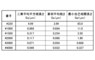
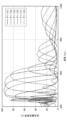
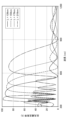
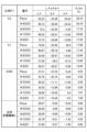
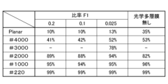
- FIG. 1 is a table showing the grit size of the abrasive used in the sandblasting method and the surface roughness of the first surface 121 of the transparent substrate 12 processed therewith. 1 is a graph showing reflection spectra in an optical multilayer film 13 with different thicknesses L and ratios F1 of one unit. 1 is a graph showing reflection spectra in an optical multilayer film 13 with different thicknesses L and ratios F1 of one unit.
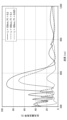
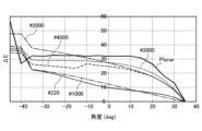
- 1 is a graph showing the angle dependency of the color exhibited in a solar cell module 1 equipped with a color adjustment plate 11.
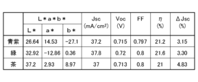
- 13 is a table summarizing the chromaticity and other properties of solar cell modules using three examples of color adjustment plates 11 that exhibit blue-purple, green, and brown.
- FIG. 1 is a schematic diagram, and the size and shape of each part are appropriately exaggerated to make it easier to understand.
- FIG. 1 is a diagram showing the layer structure of a solar cell module of the present embodiment, in which the upper side in the drawing is the light incident side (light receiving side) in the used state, and the lower side in the drawing is the back side (rear side).
- the solar cell module 1 of this embodiment includes, in order from the light incident side, a color adjustment plate 11 , a sealing material layer 14 , a solar cell element 15 , a sealing material layer 16 , and a rear surface protection plate 17 .
- the color adjustment plate 11 is a member including a transparent substrate 12 and an optical multilayer film 13.
- the color adjustment plate 11 is disposed on the light incident side of the solar cell element 15 of the solar cell module 1, with the optical multilayer film 13 side being the light incident side.
- This color adjusting plate 11 has a function of adjusting the color of the light incident surface of the solar cell module 1 .
- Fig. 2 is a diagram for explaining the optical multilayer film 13.
- Fig. 2 illustrates a flat optical multilayer film 13.
- the upper side in the drawing is the light receiving side
- the lower side is the transparent substrate 12 side.
- the optical multilayer film 13 is formed on the first surface 121 of the transparent substrate 12 so as to follow the uneven shape of the first surface 121 .
- the high refractive index layer 131 is made of titanium oxide ( TiO2 refractive index: 2.1), and the low refractive index layer 132 is made of silicon oxide ( SiO2 refractive index: 1.5).
- the materials for forming the high refractive index layer 131 and the low refractive index layer 132 may be appropriately selected according to the color to be expressed by the optical multilayer film 13, as long as they have a preferable refractive index.
- FIG. 2 an example is shown in which the layer closest to the transparent substrate 12 is the high refractive index layer 131, but this is not limiting and the layer may be the low refractive index layer 132.
- one unit is defined as a state in which one high refractive index layer 131 and one low refractive index layer 132 are stacked.
- the optical multilayer film 13 is formed by stacking five high refractive index layers 131 and five low refractive index layers 132 alternately, i.e., five units are stacked. From the viewpoint of achieving good color development, it is preferable that the optical multilayer film 13 is stacked in three or more units. Also, the greater the number of stacked units, the better the color development can be achieved, but from the viewpoint of production costs, etc., it is preferable that the optical multilayer film 13 is stacked in three to five units.
- sealing material layer 14 and 16 may be a single layer depending on the type of solar cell element 15 used in the solar cell module 1 and the structure of the solar cell module 1.
- the sealing material layers 14 and 16 in this embodiment are formed of a polyolefin resin.
- the transparent substrate 12 in this embodiment is made of optical glass, and the first surface 121 is processed by sandblasting.
- the first surface 121 of the transparent substrate 12 was sandblasted using abrasives of different grits, and the surface roughness was measured.
- the abrasives used in the sandblasting were aluminum oxide particles (Fuji Random A, manufactured by Fuji Manufacturing Co., Ltd.).
- FIG. 4 and 5 are graphs showing the reflection spectra of the optical multilayer film 13 with different unit thicknesses L and ratios F1. 4 and 5 were obtained by simulation.
- various optical simulation software such as DiffractMod by RSoft Inc. and optical thin film design software (OptiLayer) by OptiLayer Inc. can be used.
- Fig. 4 shows the reflection spectra of six examples of the optical multilayer film 13 in which the thickness L of one unit is kept constant and the ratio F1 is changed
- Fig. 5 shows the reflection spectra of four examples of the optical multilayer film 13 in which the thickness L of one unit is kept constant and the ratio F1 is changed.
- the vertical axis represents the total light reflectance [%]
- the horizontal axis represents the wavelength [nm].
- the inventors By finding a suitable range for the surface roughness of the first surface 121 (particularly the root-mean-square height Sq and the minimum autocorrelation length Sal), the inventors have realized a color adjustment plate 11 that combines good color development with reduced optical loss, and further has an anti-glare effect and exhibits little color change depending on the observation angle, and a solar cell module 1 that includes the same. Furthermore, for this color adjustment plate 11, they have further found a suitable range for the ratio F1 of the optical multilayer film 13, and by combining this with the surface roughness of the first surface 121 described above, they have realized a color adjustment plate 11 that further enhances these effects, and a solar cell module 1 that includes the same.
- the measurement results shown in the table of FIG. 7 show that by roughening the first surface 121 of the transparent substrate 12 on which the optical multilayer film 13 is formed with an abrasive having a grit size of #220 or more and #3000 or less, and by setting the root mean square height Sq of the uneven shape of the first surface 121 to 0.071 ⁇ m or more and 4.99 ⁇ m or less, and the minimum autocorrelation length Sal to 0.688 ⁇ m or more and 85.0 ⁇ m or less, it is possible to realize a color adjustment plate 11 and a solar cell module 1 that exhibit good color development while suppressing optical loss.
- the color adjustment plate 11 has an anti-glare effect.
- the diffuse reflectance of each color adjustment plate 11 was measured as an index of this anti-glare effect. The higher the diffuse reflectance, the lower the regular reflectance. Therefore, a higher diffuse reflectance indicates a higher proportion of diffusely reflected light and a higher anti-glare effect. From the viewpoint of exerting a high anti-glare effect, it is preferable that this diffuse reflectance is 80% or more.
- the optical multilayer film 13 there are four examples in total: an example without the optical multilayer film 13, and an example with the optical multilayer film 13 and with the ratio F1 of 0.025, 0.1, and 0.2.
- the color adjustment plate 11 with a planar first surface 121 had a large angle dependency, with an angle range where ⁇ E ⁇ 25 being only about 10 degrees. However, by roughening the first surface 121, the angle range where ⁇ E ⁇ 25 was expanded to more than 20 degrees. Furthermore, when the surface roughness of the first surface 121 was large, such as in the case of a color adjustment plate 11 with the first surface 121 roughened using abrasives with grit sizes #220 and #1000, the angle range where ⁇ E ⁇ 25 was expanded further to more than 70 degrees, and the angle dependency became smaller.
- the color adjustment plate 11 has a small surface roughness of the uneven shape of the first surface 121.
- the first surface 121 is preferably roughened by an abrasive having a grit size of #220 or more and #3000 or less.
- the color adjustment plate 11 has a large surface roughness of the uneven shape of the first surface 121.
- the first surface 121 is preferably roughened with an abrasive having a grit size of #220 or more and #2000 or less.
- the first surface 121 is a rough surface and that the surface roughness of the uneven shape is large.
- the first surface 121 is preferably roughened by an abrasive having a grit size of #220 or more and #4000 or less.
- the color adjustment plate 11 and solar cell module 1 of this embodiment have a transparent substrate 12 in which the first surface 121 is roughened with an abrasive having a grit size of #220 or more and #2000 or less, the root mean square height Sq of the uneven shape of the first surface 121 is 0.117 ⁇ m or more and 4.99 ⁇ m or less, and the minimum autocorrelation length Sal is 1.86 ⁇ m or more and 85.0 ⁇ m or less, and an optical multilayer film 13 is formed on this roughened first surface 121, so that it is possible to express a good color with high visibility, improve the design, have an anti-glare effect, and reduce optical loss to improve power generation efficiency.
- the color adjustment plate 11 and the solar cell module 1 are described as being green in color, but for other colors, by satisfying the above conditions, the color adjustment plate 11 and the solar cell module can be made to have small current loss and achieve clear color development.
- FIG. 10 is a table summarizing the chromaticity and other properties of solar cell modules using three examples of color adjustment plates 11 that exhibit blue-purple, green, and brown.
- the three examples of color adjusting plates 11 have their color development adjusted based on the technical concept of this embodiment as described above, and the color adjusting plates 11 and the solar cell modules 1 have substantially the same configuration.
- Jsc is the short-circuit current [mA/cm 2 ]
- Voc is the open circuit voltage [V]
- FF is the fill factor
- ⁇ is the conversion efficiency [%]
- ⁇ Jsc is the current loss [%] as described above.
- the first surface 121 of each of the blue-purple, green, and brown color adjustment plates 11 has been roughened by sandblasting with a grit #2000 abrasive, and the root mean square height Sq of the uneven shape of the first surface 121 is 0.117 ⁇ m, and the minimum autocorrelation length Sal is 1.86 ⁇ m.
- the solar cell module 1 may be configured to have a color adjustment plate 11, a solar cell element 15, a sealing material layer 16, and a back surface protective plate 17 laminated in this order from the light incident side.
- the surface of the solar cell element 15 facing the transparent substrate 12 is not covered with the sealing material layer, and the electrodes, lead wires, etc. of the solar cell element 15 are disposed on the back surface side (back surface protective plate 17 side) of the solar cell element 15.
- the solar cell element 15 may be a thin-film solar cell element that can be directly formed on the back surface side of the color adjustment plate 11 itself as a substrate, and for example, a CdTe solar cell element, some thin-film silicon solar cell element, or a perovskite solar cell element is suitable.
- the solar cell element 15 may be integrally formed on the front surface side of the rear surface protective plate 17, and the encapsulant layer and the color adjustment plate 11 may be laminated on the front surface side.
- the solar cell element 15 may be a thin-film solar cell element formed on an opaque substrate, and for example, a CIS solar cell, some thin-film silicon solar cell element, perovskite solar cell element, etc. may be used.
- the color adjustment plate 11 is arranged as the light-entering substrate of the two substrates that sandwich the solar cell element in the solar cell module.
- the present invention is not limited to this.
- the two substrates may be made of a resin film or the like, and the color adjustment plate 11 may be arranged on the light-entering side of the light-entering substrate.
- the optical multilayer film 13 is provided on the light-entering side of the transparent substrate 12 in the above example, it may be provided on the back side of the transparent substrate 12, i.e., on the sealing material layer 14 side.
- the second surface 122 is a rough surface having a fine and irregular uneven shape.
- the root-mean-square height Sq and the minimum autocorrelation length Sal of the uneven shape satisfy the numerical ranges shown in the above embodiment, so that it is possible to obtain a good color adjustment plate 11 and solar cell module 1 having good color development and small current loss.
- the thickness L and ratio F1 of one unit, the material of the layer of the optical multilayer film closest to the transparent substrate 12, etc. may be appropriately adjusted.
- a protective sheet made of resin or glass with high light transmittance may be provided on the light incident side of the color adjustment plate 11 to protect the color adjustment plate 11. Also, a protective layer made of resin with high light transmittance may be formed on the light incident side of the optical multilayer film 13.
Landscapes
- Physics & Mathematics (AREA)
- General Physics & Mathematics (AREA)
- Optics & Photonics (AREA)
- Photovoltaic Devices (AREA)
Priority Applications (1)
| Application Number | Priority Date | Filing Date | Title |
|---|---|---|---|
| JP2025520416A JPWO2024236902A1 (enExample) | 2023-05-17 | 2024-03-25 |
Applications Claiming Priority (2)
| Application Number | Priority Date | Filing Date | Title |
|---|---|---|---|
| JP2023-081616 | 2023-05-17 | ||
| JP2023081616 | 2023-05-17 |
Publications (1)
| Publication Number | Publication Date |
|---|---|
| WO2024236902A1 true WO2024236902A1 (ja) | 2024-11-21 |
Family
ID=93518908
Family Applications (1)
| Application Number | Title | Priority Date | Filing Date |
|---|---|---|---|
| PCT/JP2024/011598 Pending WO2024236902A1 (ja) | 2023-05-17 | 2024-03-25 | 色調整板及び太陽電池モジュール |
Country Status (2)
| Country | Link |
|---|---|
| JP (1) | JPWO2024236902A1 (enExample) |
| WO (1) | WO2024236902A1 (enExample) |
Citations (8)
| Publication number | Priority date | Publication date | Assignee | Title |
|---|---|---|---|---|
| JP2008238646A (ja) * | 2007-03-28 | 2008-10-09 | Toray Ind Inc | ハードコートフィルムおよび反射防止フィルム |
| JP2012003027A (ja) * | 2010-06-16 | 2012-01-05 | Sony Corp | 光学体、壁材、建具、および日射遮蔽装置 |
| JP2014107504A (ja) * | 2012-11-29 | 2014-06-09 | Panasonic Corp | 光起電力装置 |
| JP2016500799A (ja) * | 2012-09-20 | 2016-01-14 | スイスインソ・ソシエテ・アノニム | 太陽エネルギーシステムに適した着色反射および高日射透過率を有する積層グレージング(laminatedglazing) |
| US20170123122A1 (en) * | 2014-04-10 | 2017-05-04 | CSEM Centre Suisse d'Electronique et de Microtechnique SA - Recherche et Développement | Infrared transmitting cover sheet |
| JP2019109414A (ja) * | 2017-12-20 | 2019-07-04 | 凸版印刷株式会社 | 発色構造体、表示体、発色構造体の製造方法 |
| KR20220164902A (ko) * | 2021-06-07 | 2022-12-14 | (주)옥토끼이미징 | 태양광 투과도가 향상된 유리를 이용한 컬러 태양광 모듈 |
| JP2023086720A (ja) * | 2021-12-10 | 2023-06-22 | 国立大学法人東京工業大学 | 色調整板、太陽電池モジュール、色調整板の製造方法、成膜方法、及び、成膜装置 |
-
2024
- 2024-03-25 WO PCT/JP2024/011598 patent/WO2024236902A1/ja active Pending
- 2024-03-25 JP JP2025520416A patent/JPWO2024236902A1/ja active Pending
Patent Citations (8)
| Publication number | Priority date | Publication date | Assignee | Title |
|---|---|---|---|---|
| JP2008238646A (ja) * | 2007-03-28 | 2008-10-09 | Toray Ind Inc | ハードコートフィルムおよび反射防止フィルム |
| JP2012003027A (ja) * | 2010-06-16 | 2012-01-05 | Sony Corp | 光学体、壁材、建具、および日射遮蔽装置 |
| JP2016500799A (ja) * | 2012-09-20 | 2016-01-14 | スイスインソ・ソシエテ・アノニム | 太陽エネルギーシステムに適した着色反射および高日射透過率を有する積層グレージング(laminatedglazing) |
| JP2014107504A (ja) * | 2012-11-29 | 2014-06-09 | Panasonic Corp | 光起電力装置 |
| US20170123122A1 (en) * | 2014-04-10 | 2017-05-04 | CSEM Centre Suisse d'Electronique et de Microtechnique SA - Recherche et Développement | Infrared transmitting cover sheet |
| JP2019109414A (ja) * | 2017-12-20 | 2019-07-04 | 凸版印刷株式会社 | 発色構造体、表示体、発色構造体の製造方法 |
| KR20220164902A (ko) * | 2021-06-07 | 2022-12-14 | (주)옥토끼이미징 | 태양광 투과도가 향상된 유리를 이용한 컬러 태양광 모듈 |
| JP2023086720A (ja) * | 2021-12-10 | 2023-06-22 | 国立大学法人東京工業大学 | 色調整板、太陽電池モジュール、色調整板の製造方法、成膜方法、及び、成膜装置 |
Also Published As
| Publication number | Publication date |
|---|---|
| JPWO2024236902A1 (enExample) | 2024-11-21 |
Similar Documents
| Publication | Publication Date | Title |
|---|---|---|
| Bläsi et al. | The morphocolor concept for colored photovoltaic modules | |
| US12040738B2 (en) | Glazing unit, method for the production thereof and use thereof | |
| US10953635B2 (en) | Laminated glazing with coloured reflection and high solar transmittance suitable for solar energy systems | |
| JP7307148B2 (ja) | パターン化したカバープレートと光干渉層とを備えたソーラーモジュール | |
| EP3625831B1 (en) | Uniformly and directionally colored photovoltaic modules | |
| JP7290710B2 (ja) | パターン化したカバープレートと光干渉層とを備えたソーラーモジュール | |
| CN109659373B (zh) | 有色太阳能板及包括该有色太阳能板的结构 | |
| CN105144397A (zh) | 太阳能光伏模块 | |
| KR20200112138A (ko) | Bipv용 컬러 태양광 모듈 및 그 제조방법 | |
| WO2017090056A1 (en) | Solar module with selective colored coating | |
| Manwani et al. | Development of novel orange colored photovoltaic modules with improved angular stability and high energy efficiency | |
| JP7526799B2 (ja) | 構造化カバープレート及びカラーフィルタ層を有するカラープレート状部品 | |
| WO2024236902A1 (ja) | 色調整板及び太陽電池モジュール | |
| US11745473B2 (en) | Laminated glazing with coloured reflection and high solar transmittance, and solar energy systems employing the same | |
| JP2019197880A (ja) | ソーラーモジュール | |
| EP2806464B1 (en) | Colored solar cells and panels containing the same | |
| CN114864728A (zh) | 一种高透光咖色玻璃以及咖色太阳能组件 | |
| JP6661664B2 (ja) | 太陽電池モジュール | |
| TWI590479B (zh) | 高反射率金色單晶矽太陽能電池及含有該電池之面板 | |
| Elsehrawy et al. | Structural color coatings for single junction and multijunction solar cells-optical spectroscopy, colorimetric photography, and power loss analysis | |
| HK40024441B (zh) | 均匀且定向着色的光伏模块 | |
| HK1208844B (en) | Laminated glazing with coloured reflection and high solar transmittance suitable for solar energy systems |
Legal Events
| Date | Code | Title | Description |
|---|---|---|---|
| 121 | Ep: the epo has been informed by wipo that ep was designated in this application |
Ref document number: 24806857 Country of ref document: EP Kind code of ref document: A1 |
|
| ENP | Entry into the national phase |
Ref document number: 2025520416 Country of ref document: JP Kind code of ref document: A |
|
| WWE | Wipo information: entry into national phase |
Ref document number: 2025520416 Country of ref document: JP |