WO2024232252A1 - 炭化珪素エピタキシャル基板および炭化珪素半導体装置の製造方法 - Google Patents
炭化珪素エピタキシャル基板および炭化珪素半導体装置の製造方法 Download PDFInfo
- Publication number
- WO2024232252A1 WO2024232252A1 PCT/JP2024/015727 JP2024015727W WO2024232252A1 WO 2024232252 A1 WO2024232252 A1 WO 2024232252A1 JP 2024015727 W JP2024015727 W JP 2024015727W WO 2024232252 A1 WO2024232252 A1 WO 2024232252A1
- Authority
- WO
- WIPO (PCT)
- Prior art keywords
- silicon carbide
- defects
- main surface
- carbide epitaxial
- gas
- Prior art date
- Legal status (The legal status is an assumption and is not a legal conclusion. Google has not performed a legal analysis and makes no representation as to the accuracy of the status listed.)
- Ceased
Links
Images










Classifications
-
- C—CHEMISTRY; METALLURGY
- C30—CRYSTAL GROWTH
- C30B—SINGLE-CRYSTAL GROWTH; UNIDIRECTIONAL SOLIDIFICATION OF EUTECTIC MATERIAL OR UNIDIRECTIONAL DEMIXING OF EUTECTOID MATERIAL; REFINING BY ZONE-MELTING OF MATERIAL; PRODUCTION OF A HOMOGENEOUS POLYCRYSTALLINE MATERIAL WITH DEFINED STRUCTURE; SINGLE CRYSTALS OR HOMOGENEOUS POLYCRYSTALLINE MATERIAL WITH DEFINED STRUCTURE; AFTER-TREATMENT OF SINGLE CRYSTALS OR A HOMOGENEOUS POLYCRYSTALLINE MATERIAL WITH DEFINED STRUCTURE; APPARATUS THEREFOR
- C30B29/00—Single crystals or homogeneous polycrystalline material with defined structure characterised by the material or by their shape
- C30B29/10—Inorganic compounds or compositions
- C30B29/36—Carbides
-
- H—ELECTRICITY
- H10—SEMICONDUCTOR DEVICES; ELECTRIC SOLID-STATE DEVICES NOT OTHERWISE PROVIDED FOR
- H10D—INORGANIC ELECTRIC SEMICONDUCTOR DEVICES
- H10D30/00—Field-effect transistors [FET]
- H10D30/01—Manufacture or treatment
- H10D30/021—Manufacture or treatment of FETs having insulated gates [IGFET]
-
- H—ELECTRICITY
- H10—SEMICONDUCTOR DEVICES; ELECTRIC SOLID-STATE DEVICES NOT OTHERWISE PROVIDED FOR
- H10D—INORGANIC ELECTRIC SEMICONDUCTOR DEVICES
- H10D30/00—Field-effect transistors [FET]
- H10D30/60—Insulated-gate field-effect transistors [IGFET]
-
- H—ELECTRICITY
- H10—SEMICONDUCTOR DEVICES; ELECTRIC SOLID-STATE DEVICES NOT OTHERWISE PROVIDED FOR
- H10P—GENERIC PROCESSES OR APPARATUS FOR THE MANUFACTURE OR TREATMENT OF DEVICES COVERED BY CLASS H10
- H10P14/00—Formation of materials, e.g. in the shape of layers or pillars
- H10P14/20—Formation of materials, e.g. in the shape of layers or pillars of semiconductor materials
- H10P14/29—Formation of materials, e.g. in the shape of layers or pillars of semiconductor materials characterised by the substrates
-
- H—ELECTRICITY
- H10—SEMICONDUCTOR DEVICES; ELECTRIC SOLID-STATE DEVICES NOT OTHERWISE PROVIDED FOR
- H10D—INORGANIC ELECTRIC SEMICONDUCTOR DEVICES
- H10D62/00—Semiconductor bodies, or regions thereof, of devices having potential barriers
- H10D62/80—Semiconductor bodies, or regions thereof, of devices having potential barriers characterised by the materials
Definitions
- This disclosure relates to a silicon carbide epitaxial substrate and a method for manufacturing a silicon carbide semiconductor device.
- This application claims priority to Japanese Patent Application No. 2023-078635, filed on May 11, 2023. All contents of said Japanese patent application are incorporated herein by reference.
- Patent Document 1 JP 2020-072156 A (Patent Document 1) describes a method for manufacturing a silicon carbide semiconductor device that uses a confocal scanning device to derive a contrast value on the surface of an epitaxial layer.
- a silicon carbide epitaxial substrate includes a silicon carbide substrate, a silicon carbide epitaxial layer, and a plurality of defects.
- the silicon carbide epitaxial layer is provided on the silicon carbide substrate.
- the plurality of defects are formed in the silicon carbide epitaxial layer.
- the silicon carbide epitaxial layer constitutes a main surface. Each of the plurality of defects is exposed on the main surface.
- Each of the plurality of defects has a contrast value of 90 or more when photographed using a confocal scanning device.
- the surface density of the plurality of defects is 2/cm2 or less. When viewed along a straight line perpendicular to the main surface, each of the plurality of defects has an area of 50 ⁇ m2 or more .
- FIG. 1 is a plan view showing a configuration of a silicon carbide epitaxial substrate according to this embodiment.
- FIG. 2 is a schematic cross-sectional view taken along line II-II in FIG.
- FIG. 3 is an enlarged schematic plan view showing region III in FIG.
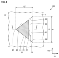
- FIG. 4 is an enlarged schematic plan view showing region IV in FIG.
- FIG. 5 is a schematic cross-sectional view taken along line VV in FIG.
- FIG. 6 is an enlarged schematic plan view showing region VI in FIG.
- FIG. 7 is a schematic cross-sectional view taken along line VII-VII in FIG.
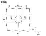
- FIG. 8 is an enlarged schematic plan view showing region VIII in FIG.
- FIG. 9 is a schematic cross-sectional view taken along line IX-IX in FIG.
- FIG. 1 is a plan view showing a configuration of a silicon carbide epitaxial substrate according to this embodiment.
- FIG. 2 is a schematic cross-sectional view taken along line II-II in FIG.
- FIG. 3 is an
- FIG. 10 is a schematic cross-sectional view showing a state in which the first main surface and the triangular defect are irradiated with light.
- FIG. 11 is a schematic diagram showing a process of identifying a defect.
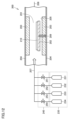
- FIG. 12 is a partial schematic cross-sectional view showing the configuration of an apparatus for manufacturing a silicon carbide epitaxial substrate.
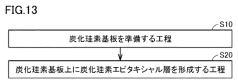
- FIG. 13 is a flow diagram illustrating a method for manufacturing a silicon carbide epitaxial substrate according to the present embodiment.
- FIG. 14 is a schematic cross-sectional view showing a step of preparing a silicon carbide substrate.
- FIG. 15 is a flow diagram illustrating a schematic method for manufacturing a silicon carbide semiconductor device according to this embodiment.
- FIG. 16 is a schematic cross-sectional view showing a step of forming a body region.
- FIG. 17 is a schematic cross-sectional view showing a step of forming a source region.
- FIG. 18 is a schematic cross-sectional view showing a step of forming a trench in the first main surface of the silicon carbide epitaxial layer.
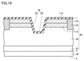
- FIG. 19 is a schematic cross-sectional view showing a step of forming a gate insulating film.
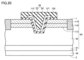
- FIG. 20 is a schematic cross-sectional view showing a step of forming a gate electrode and an interlayer insulating film.
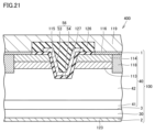
- FIG. 21 is a schematic cross-sectional view showing the configuration of a silicon carbide semiconductor device according to this embodiment.
- FIG. 21 is a schematic cross-sectional view showing the configuration of a silicon carbide semiconductor device according to this embodiment.
- FIG. 22 is a graph showing the surface density of defects having a contrast value of 90 or more and the hydrogen flow rate ratio in Samples 1 to 14.
- FIG. 23 is a graph showing the surface density of defects having a contrast value of 120 or more and the hydrogen flow rate ratio in Samples 1 to 14.
- FIG. 24 is a graph showing the surface density of defects having a contrast value of 150 or more and the hydrogen flow rate ratio in Samples 1 to 14.
- FIG. 25 is a graph showing the areal density of defects having a contrast value of 90 or more in Samples 1 to 14 versus the growth temperature/hydrogen flow rate.
- FIG. 26 is a graph showing the areal density of defects having a contrast value of 120 or more in Samples 1 to 14 versus the growth temperature/hydrogen flow rate.
- FIG. 27 is a graph showing the areal density of defects having a contrast value of 150 or more in Samples 1 to 14 versus the growth temperature/hydrogen flow rate.
- An object of the present disclosure is to provide a silicon carbide epitaxial substrate and a method for manufacturing a silicon carbide semiconductor device that are capable of improving the yield of silicon carbide semiconductor devices.
- the present disclosure can provide a silicon carbide epitaxial substrate and a method for manufacturing a silicon carbide semiconductor device that can improve the yield of silicon carbide semiconductor devices.
- a silicon carbide epitaxial substrate includes a silicon carbide substrate, a silicon carbide epitaxial layer, and a plurality of defects.
- the silicon carbide epitaxial layer is provided on the silicon carbide substrate.
- the plurality of defects are formed in the silicon carbide epitaxial layer.
- the silicon carbide epitaxial layer constitutes a main surface.
- Each of the plurality of defects is exposed on the main surface.
- Each of the plurality of defects has a contrast value of 90 or more when photographed using a confocal scanning device.
- the surface density of the plurality of defects is 2/cm2 or less. When viewed along a straight line perpendicular to the main surface, each of the plurality of defects has an area of 50 ⁇ m2 or more.
- the plurality of defects may include a portion whose polytype is 3C.
- the plurality of defects and the silicon carbide epitaxial layer may form a recess.
- the plurality of defects may include at least one of bumps, pits, carrots, triangular defects, and downfalls.
- the longer of the length in a first direction and the length in a second direction perpendicular to the first direction may be 10 ⁇ m or more.
- the main surface may be in an as-grown state.
- the method for manufacturing a silicon carbide semiconductor device includes the following steps: A silicon carbide epitaxial substrate according to any one of (1) to (5) above is prepared. An electrode is formed on the silicon carbide epitaxial layer.
- FIG. 1 is a plan view schematic diagram showing a configuration of a silicon carbide epitaxial substrate 100 according to this embodiment.
- FIG. 2 is a cross-sectional schematic diagram taken along line II-II in FIG. 1.
- the silicon carbide epitaxial substrate 100 according to this embodiment has a silicon carbide substrate 30 and a silicon carbide epitaxial layer 40.
- the silicon carbide epitaxial layer 40 is provided on the silicon carbide substrate 30.
- the silicon carbide epitaxial layer 40 is in contact with the silicon carbide substrate 30.
- the silicon carbide epitaxial substrate 100 has a first main surface 1 and a second main surface 2.
- the first main surface 1 is a front surface of the silicon carbide epitaxial substrate 100.
- the second main surface 2 is opposite to the first main surface 1.
- the second main surface 2 is a rear surface of the silicon carbide epitaxial substrate 100.
- the silicon carbide epitaxial substrate 100 has an outer peripheral edge 9.
- the outer peripheral edge 9 has, for example, an orientation flat 7 and an arc-shaped portion 8.
- the orientation flat 7 extends along a first direction 101.
- the orientation flat 7 is linear when viewed along a straight line perpendicular to the first main surface 1.
- the arc-shaped portion 8 is continuous with the orientation flat 7.
- the arc-shaped portion 8 is arc-shaped when viewed along a straight line perpendicular to the first main surface 1.
- the first principal surface 1 when viewed along a straight line perpendicular to the first principal surface 1, the first principal surface 1 extends along each of a first direction 101 and a second direction 102.
- the second direction 102 is a direction perpendicular to the first direction 101.
- the first direction 101 is, for example, the ⁇ 11-20> direction.
- the first direction 101 may be, for example, the [11-20] direction.
- the first direction 101 may be a direction obtained by projecting the ⁇ 11-20> direction onto the first principal surface 1. From another perspective, the first direction 101 may be, for example, a direction that includes a ⁇ 11-20> directional component.
- the second direction 102 is, for example, the ⁇ 1-100> direction.
- the second direction 102 may be, for example, the [1-100] direction.
- the second direction 102 may be, for example, a direction obtained by projecting the ⁇ 1-100> direction onto the first principal surface 1. From another perspective, the second direction 102 may be, for example, a direction that includes a ⁇ 1-100> directional component.
- the first main surface 1 is a surface inclined with respect to the ⁇ 0001 ⁇ surface.
- the inclination angle (off angle) with respect to the ⁇ 0001 ⁇ surface is, for example, greater than 0° and equal to or less than 8°.
- the off angle is not particularly limited, but may be, for example, 1° or more, or 2° or more.
- the off angle is not particularly limited, but may be, for example, 7° or less, or 6° or less.
- the first main surface 1 may be a surface inclined by the off angle with respect to the (000-1) surface, or may be a surface inclined by the off angle with respect to the (0001) surface.
- the inclination direction (off direction) of the first main surface 1 is, for example, the ⁇ 11-20> direction.
- the maximum diameter W of the first main surface 1 is not particularly limited, but is, for example, 100 mm (4 inches) or more.
- the maximum diameter W may be 125 mm (5 inches) or more, or 150 mm (6 inches) or more.
- the maximum diameter W may be, for example, 200 mm (8 inches) or less.
- the maximum diameter W is the maximum distance between any two points on the outer circumferential edge 9.
- 4 inches means 100 mm or 101.6 mm (4 inches x 25.4 mm/inch). 5 inches means 125 mm or 127.0 mm (5 inches x 25.4 mm/inch). 6 inches means 150 mm or 152.4 mm (6 inches x 25.4 mm/inch). 8 inches means 200 mm or 203.2 mm (8 inches x 25.4 mm/inch).
- the silicon carbide substrate 30 constitutes a second main surface 2.
- the second main surface 2 is provided opposite the interface 3 between the silicon carbide substrate 30 and the silicon carbide epitaxial layer 40.
- the polytype of the silicon carbide constituting the silicon carbide substrate 30 is, for example, 4H.
- the silicon carbide epitaxial layer 40 constitutes a first main surface 1.
- the first main surface 1 is provided opposite the interface 3.
- the silicon carbide epitaxial layer 40 has a buffer layer 41 and a drift layer 42.
- the drift layer 42 may be a single layer or may be two or more layers.
- the polytype of the silicon carbide constituting the silicon carbide epitaxial layer 40 is, for example, 4H.
- the first main surface 1 is in an as-grown state.
- the as-grown state refers to a state after epitaxial growth and in which the silicon carbide epitaxial layer 40 has not been polished.
- the first main surface 1 is in an epitaxially grown state. From another perspective, the first main surface 1 is an unpolished surface.
- the first main surface 1 can be said to be in an as-grown state.
- An example of a treatment that does not modify the SiC surface state is cleaning.
- the buffer layer 41 is provided on the silicon carbide substrate 30.
- the buffer layer 41 is in contact with the silicon carbide substrate 30.
- the drift layer 42 is provided on the buffer layer 41.
- the drift layer 42 is in contact with the buffer layer 41.
- the drift layer 42 constitutes the first main surface 1.
- the third direction 103 is a direction from the second main surface 2 toward the first main surface 1.
- the third direction 103 is perpendicular to both the first direction 101 and the second direction 102.
- the cross section shown in FIG. 2 is perpendicular to the first main surface 1 and parallel to the first direction 101.
- the silicon carbide substrate 30 contains an n-type impurity such as nitrogen (N).
- the conductivity type of the silicon carbide substrate 30 is, for example, n-type.
- the thickness of the silicon carbide substrate 30 in the third direction 103 is, for example, 200 ⁇ m or more and 600 ⁇ m or less.
- the silicon carbide epitaxial layer 40 contains an n-type impurity such as nitrogen.
- the conductivity type of the silicon carbide epitaxial layer 40 is, for example, n-type.
- the concentration of n-type impurities contained in buffer layer 41 may be lower than the concentration of n-type impurities contained in silicon carbide substrate 30.
- the concentration of n-type impurities contained in buffer layer 41 is, for example, 1 ⁇ 10 18 atoms/cm 3 or more and 1 ⁇ 10 19 atoms/cm 3 or less.
- the thickness of buffer layer 41 in third direction 103 is, for example, 0.1 ⁇ m or more and 10 ⁇ m or less.
- the concentration of n-type impurities contained in drift layer 42 may be lower than the concentration of n-type impurities contained in buffer layer 41.
- the concentration of n-type impurities contained in drift layer 42 is, for example, 1 ⁇ 10 15 atoms/cm 3 or more and 1 ⁇ 10 17 atoms/cm 3 or less.
- the thickness of drift layer 42 in third direction 103 is, for example, 5 ⁇ m or more and 30 ⁇ m or less.
- FIG. 3 is an enlarged schematic plan view showing region III in FIG. 1.
- the silicon carbide epitaxial substrate 100 has a defect 90.
- the defect 90 is exposed on the first main surface 1.
- the defect 90 has at least one of the bump 60, the pit 50, the carrot 72, the triangular defect 20, and the downfall 71. Details of the bump 60, the pit 50, the carrot 72, the triangular defect 20, and the downfall 71 will be described later.
- the defect 90 is formed in the silicon carbide epitaxial layer 40 (see FIG. 2).
- the defect 90 forms a recess or a protrusion.
- the first main surface 1 has a flat portion 10.
- the flat portion 10 is a portion of the first main surface 1 where the defect 90 is not exposed.
- Fig. 4 is an enlarged schematic plan view showing region IV in Fig. 1.
- the enlarged schematic plan view shown in Fig. 4 shows a state observed by a confocal scanning device.
- silicon carbide epitaxial substrate 100 according to this embodiment has triangular defect 20.
- triangular defect 20 when viewed along a straight line perpendicular to first main surface 1, triangular defect 20 has, for example, a triangular shape.
- FIG. 5 is a schematic cross-sectional view taken along line V-V in FIG. 4.
- the cross section shown in FIG. 5 is perpendicular to the first main surface 1.
- a first recess 29 is formed in the first main surface 1 of the silicon carbide epitaxial substrate 100 according to this embodiment.
- the first recess 29 is composed of a silicon carbide epitaxial layer 40 and a triangular defect 20.
- the outer shape of the first recess 29 is triangular.
- the defect 90 may include the triangular defect 20 and the first recess 29.
- triangular defect 20 has first side portion 23, second side portion 24, first base portion 22, and top surface portion 25.
- Second side portion 24 is connected to first side portion 23.
- the boundary between second side portion 24 and first side portion 23 is vertex 21.
- First side portion 23 and second side portion 24 branch into two from vertex 21.
- First base portion 22 is connected to each of first side portion 23 and second side portion 24.
- First side portion 23 is connected to one end (first end portion) of first base portion 22, and second side portion 24 is connected to the other end (second end portion) of first base portion 22.
- Top surface portion 25 is surrounded by first side portion 23, second side portion 24, and first base portion 22. When viewed along a straight line perpendicular to the first main surface 1, the shape of the top surface 25 is triangular.
- the first side portion 23 When viewed along a line perpendicular to the first main surface 1, the first side portion 23 is inclined with respect to each of the first direction 101 and the second direction 102.
- the first side portion 23 may be inclined from a line parallel to the first direction 101 toward the second direction 102.
- the second side portion 24 may be inclined from a line parallel to the first direction 101 in a direction opposite to the second direction 102.
- the first base portion 22 When viewed along a line perpendicular to the first main surface 1, the first base portion 22 extends along the second direction 102.
- the width of the triangular defect 20 in the second direction 102 may increase from the apex 21 toward the first base portion 22.
- the silicon carbide epitaxial layer 40 has a third side portion 63, a fourth side portion 64, and a second base portion 62.
- a portion of the third side portion 63 may overlap the first side portion 23 of the triangular defect 20.
- a portion of the fourth side portion 64 may overlap the second side portion 24 of the triangular defect 20.
- the fourth side portion 64 when viewed along a line perpendicular to the first main surface 1, the fourth side portion 64 is connected to the third side portion 63 at the vertex 21. From another perspective, when viewed along a line perpendicular to the first main surface 1, the third side portion 63 and the fourth side portion 64 branch into two from the vertex 21.
- the second base portion 62 is connected to each of the third side portion 63 and the fourth side portion 64.
- the third side portion 63 is connected to one end (third end portion) of the second base portion 62, and the fourth side portion 64 is connected to the other end (fourth end portion) of the second base portion 62.
- the third side portion 63 When viewed along a straight line perpendicular to the first main surface 1, the third side portion 63 is inclined with respect to each of the first direction 101 and the second direction 102.
- the third side portion 63 may be inclined from a straight line parallel to the first direction 101 toward the second direction 102.
- the third side portion 63 may be substantially parallel to the first side portion 23 of the triangular defect 20.
- the fourth side portion 64 may be inclined from a straight line parallel to the first direction 101 in a direction opposite to the second direction 102.
- the fourth side portion 64 may be substantially parallel to the second side portion 24 of the triangular defect 20.
- the second base portion 62 When viewed along a straight line perpendicular to the first main surface 1, the second base portion 62 extends along the second direction 102.
- the second base portion 62 When viewed along a straight line perpendicular to the first main surface 1, the second base portion 62 may be substantially parallel to the first base portion 22 of the triangular defect 20. When viewed along a straight line perpendicular to the first main surface 1, the second base portion 62 is in the first direction 101 relative to the first base portion 22.
- the length of the first recess 29 in the first direction 101 as viewed along a straight line perpendicular to the first main surface 1 is defined as a first length A1.
- the first length A1 is the maximum distance between the apex 21 and the second base 62 as viewed in a direction perpendicular to the first main surface 1.
- the defect 90 is a triangular defect 20
- the first length A1 is defined as the length of the defect 90 in the first direction 101.
- the length of the first recess 29 in the second direction 102 is defined as a first width B1.
- the first width B1 may be equal to the length of the second base 62.
- the first width B1 is defined as the length of the defect 90 in the second direction 102.
- the longer of the first length A1 and the first width B1 (first measured length) is, for example, 10 ⁇ m or more and 80 ⁇ m or less.
- the ratio of the first width B1 to the first length A1 is, for example, 0.5 or more and 5 or less.
- the ratio of the first width B1 to the first length A1 is not particularly limited, but may be, for example, 0.8 or more, or 1.2 or more.
- the ratio of the first width B1 to the first length A1 is not particularly limited, but may be, for example, 4 or less, or 3 or less.
- the triangular defect 20 may have a first side portion 27 and a bottom portion 26.
- the first side portion 27 extends along the third direction 103.
- the bottom portion 26 extends along the fourth direction 104.
- the surface extending along the fourth direction 104 is the base surface.
- the bottom portion 26 is continuous with the first side portion 27.
- the boundary between the bottom portion 26 and the first side portion 27 is defined as the starting point 28.
- the fourth direction 104 is inclined with respect to both the first direction 101 and the third direction 103.
- the fourth direction 104 is inclined toward the third direction 103 with respect to the first direction 101.
- the angle between the fourth direction 104 and the first direction 101 is the off angle ⁇ .
- the top surface portion 25 is connected to each of the bottom surface portion 26 and the first side surface portion 27.
- the top surface portion 25 extends along the first direction 101.
- the top surface portion 25 may be substantially parallel to the first main surface 1.
- the top surface portion 25 forms the bottom surface of the first recess 29.
- the surface orientation of the top surface portion 25 may be the same as the surface orientation of the first main surface 1.
- the origin 28 is, for example, in the drift layer 42. From another perspective, in the third direction 103, the origin 28 is, for example, between the first main surface 1 and the buffer layer 41. The origin 28 may be in the buffer layer 41. The length of the triangular defect 20 in the first direction 101 may increase from the origin 28 toward the top surface portion 25.
- the silicon carbide epitaxial layer 40 has a second side portion 67 and a third side portion 66.
- the second side portion 67 may extend along the third direction 103.
- the second side portion 67 may extend along the first side portion 27 of the triangular defect 20.
- the third side portion 66 is connected to the second side portion 67.
- the third side portion 66 extends along the fourth direction 104.
- the third side portion 66 may extend along the bottom surface portion 26 of the triangular defect 20.
- the second side portion 67 and the third side portion 66 form the side surfaces of the first recess 29.
- the first recess 29 is defined by the top surface 25 of the triangular defect 20 and the second side surface 67 and third side surface 66 of the silicon carbide epitaxial layer 40. From another perspective, the bottom surface of the first recess 29 is formed by the triangular defect 20. The side surface of the first recess 29 is formed by the silicon carbide epitaxial layer 40.
- the polytype of silicon carbide that constitutes triangular defect 20 is different from the polytype of silicon carbide that constitutes silicon carbide epitaxial layer 40. From another perspective, the polytype of silicon carbide that constitutes the bottom surface of first recess 29 is different from the polytype of silicon carbide that constitutes silicon carbide epitaxial layer 40.
- the polytype of silicon carbide that constitutes triangular defect 20 is, for example, 3C.
- the depth of the first recess 29 in the third direction 103 is a first depth C1.
- the first depth C1 is the distance between the flat portion 10 and the top surface portion 25 in the third direction 103.
- the first depth C1 is not particularly limited, but is, for example, 0.01 ⁇ m or more and 10 ⁇ m or less.
- the first depth C1 can be measured, for example, using a Nikon white light interference microscope (product name "BW-D507").
- a mercury lamp is used as the light source.
- the measurement field of view is 256 ⁇ m x 256 ⁇ m.
- the light emitted from the light source is split into two by a beam splitter. One light is irradiated onto the reference surface. The other light is irradiated onto the first principal surface 1 and the top surface portion 25. The light reflected from both is imaged by a camera.
- the first depth C1 is measured based on information about interference fringes obtained from the optical path difference caused by the unevenness formed on the first principal surface 1 and the top surface portion 25.
- the area of the defect 90 is the sum (first area) of the area of the top surface portion 25 and the area of the third side surface portion 66 when viewed along a straight line perpendicular to the first main surface 1.
- the first area is 50 ⁇ m 2 or more.
- the first area may be, for example, 6200 ⁇ m 2 or less.
- Fig. 6 is an enlarged schematic plan view showing region VI in Fig. 1.
- the enlarged schematic plan view shown in Fig. 6 shows a state observed by a confocal scanning device.
- pits 50 may be present in first main surface 1 of silicon carbide epitaxial substrate 100.
- the shape of pit 50 as viewed along a straight line perpendicular to first main surface 1 is not particularly limited, but may be, for example, substantially circular.
- the length of the pit 50 in the first direction 101 is the second length A2.
- the length of the pit 50 in the second direction 102 is the second width B2.
- the longer length (second measurement length) is, for example, 10 ⁇ m or more and 50 ⁇ m or less.
- the value obtained by dividing the second length A2 by the second width B2 is not particularly limited, and may be, for example, 0.1 to 10, or 0.2 to 5.
- the shape of the pit 50 may be, for example, rod-like.
- the area of the pit 50 is 50 ⁇ m 2 or more.
- the area of the pit 50 may be, for example, 100 ⁇ m 2 or less.
- FIG. 7 is a schematic cross-sectional view taken along line VII-VII in FIG. 6.
- the cross section shown in FIG. 7 is perpendicular to the first main surface 1.
- the pit 50 is a depression formed in the first main surface 1.
- the side surfaces constituting the pit 50 may be curved.
- the depth of the pit 50 in the third direction 103 is set to a second depth C2.
- the second depth C2 is not particularly limited, but is, for example, 0.01 ⁇ m or more and 0.1 ⁇ m or less.
- Fig. 8 is an enlarged schematic plan view showing region VIII in Fig. 1.
- the enlarged schematic plan view shown in Fig. 8 shows a state observed by a confocal scanning device.
- bump 60 may be present on first main surface 1 of silicon carbide epitaxial substrate 100.
- the shape of bump 60 is not particularly limited when viewed along a straight line perpendicular to first main surface 1, but may be, for example, substantially circular.
- the length of the bump 60 in the first direction 101 is a third length A3.
- the length of the bump 60 in the second direction 102 is a third width B3.
- the longer length (third measured length) is, for example, 10 ⁇ m or more and 50 ⁇ m or less.
- the value obtained by dividing the third length A3 by the third width B3 is not particularly limited, and may be, for example, 0.1 to 10, or 0.2 to 5.
- the shape of the bump 60 may be, for example, rod-like.
- the area of the bump 60 is 50 ⁇ m 2 or more.
- the area of the bump 60 may be, for example, 100 ⁇ m 2 or less.
- FIG. 9 is a schematic cross-sectional view taken along line IX-IX in FIG. 8.
- the cross section shown in FIG. 9 is perpendicular to the first main surface 1.
- the bump 60 is a protrusion formed on the first main surface 1.
- the bump 60 forms a convex portion on the first main surface 1.
- the side surfaces constituting the bump 60 may be curved.
- the height C3 of the bump 60 in the third direction 103 is not particularly limited, but is, for example, 0.01 ⁇ m or more and 0.1 ⁇ m or less.
- Silicon carbide epitaxial substrate 100 may have carrots 72. When viewed along a straight line perpendicular to first main surface 1, carrots 72 extend linearly along a direction inclined with respect to each of first direction 101 and second direction 102. When viewed along a straight line perpendicular to first main surface 1, carrots 72 extend, for example, along a direction inclined with respect to first direction 101.
- Carrot 72 is a recess caused by a screw dislocation. In a cross section perpendicular to the direction in which carrot 72 extends, there may be a pair of protrusions on both sides of carrot 72.
- Carrot 72 is defined by a pair of side surfaces and a bottom surface. The bottom surface is connected to each of the pair of side surfaces. A portion of the side surface is formed by the protrusions.
- the longer of the length of the carrot 72 in the first direction 101 and the length of the carrot 72 in the second direction 102 is, for example, 10 ⁇ m or more and 150 ⁇ m or less.
- the area of the carrot 72 is 50 ⁇ m2 or more .
- the area of the carrot 72 may be, for example, 900 ⁇ m2 or less.
- DOWNFALL Silicon carbide epitaxial substrate 100 may have downfall 71.
- Downfall 71 is, for example, a deposit adhering to an inner wall of a film forming apparatus that falls onto silicon carbide substrate 30.
- Downfall 71 is, for example, a particle of polycrystalline silicon carbide.
- Downfall 71 may be, for example, a carbon particle or a tantalum carbide particle.
- the downfall 71 may be on the silicon carbide substrate 30. In the third direction 103, the downfall 71 may be located between the first main surface 1 and the interface 3. Around the downfall 71, for example, a second recess is formed in the silicon carbide epitaxial layer 40. From another perspective, the downfall 71 is located in the second recess formed in the silicon carbide epitaxial layer 40.
- the longer of the length of the downfall 71 in the first direction 101 and the length of the downfall 71 in the second direction 102 is, for example, 10 ⁇ m or more and 50 ⁇ m or less.
- the area of the downfall 71 is 50 ⁇ m2 or more .
- the area of the downfall 71 may be, for example, 100 ⁇ m2 or less.
- a confocal scanning device is used to identify the defect 90.
- the confocal scanning device has a differential interference optical system.
- the confocal scanning device for example, the WASAVI series "SICA 6X” manufactured by Lasertec Corporation can be used.
- the magnification of the objective lens is, for example, 10 times.
- the contrast value of the defect 90 when the first principal surface 1 is imaged using a confocal scanning device is 90 or more.
- the contrast value of the defect 90 when the first principal surface 1 is imaged using a confocal scanning device may be, for example, 120 or more, or 150 or more.
- the contrast value of the defect 90 when the first principal surface 1 is imaged using a confocal scanning device may be, for example, 256 or less, or 230 or less.
- the area of defect 90 is 50 ⁇ m 2 or more.
- the area of defect 90 may be, for example, 500 ⁇ m 2 or more, or 1000 ⁇ m 2 or more.
- the area of defect 90 may be, for example, 5000 ⁇ m 2 or less, or 2000 ⁇ m 2 or less.
- a light source is, for example, a mercury xenon lamp.
- the wavelength of the light is, for example, 546 nm.
- the number of pixels in the captured grayscale image is, for example, 1024 pixels x 1024 pixels.
- the size of a pixel is, for example, 1 nm x 1 nm.
- pixels represent shades of black and white (brightness). Brightness is classified into 257 levels, from 0 (minimum) to 256 (maximum).
- areas with high brightness (bright areas) are displayed in white, and conversely, areas with low brightness (dark areas) are displayed in black.
- the defect 90 forms a concave or convex portion. Therefore, when light is irradiated onto the first principal surface 1, the defect 90 has brighter and darker portions compared to the flat portion 10 of the first principal surface 1.
- FIG. 10 is a schematic cross-sectional view showing a state in which light is irradiated onto the first main surface 1 and the triangular defect 20.
- the schematic cross-sectional view shown in FIG. 10 corresponds to the schematic cross-sectional view shown in FIG. 5.
- light is irradiated, for example, in a direction along the arrow R.
- the arrow R is inclined in a first direction 101 with respect to a line perpendicular to the first main surface 1, and is inclined in a second direction 102 with respect to a line perpendicular to the first main surface 1.
- the arrow R is inclined, for example, by 45° in the first direction 101 with respect to a line perpendicular to the first main surface 1.
- the arrow R is inclined, for example, by 45° in the second direction 102 with respect to a line perpendicular to the first main surface 1.
- the light irradiated to the third side portion 66 is reflected in a direction along the third direction 103, so that the third side portion 66 is brighter than the flat portion 10.
- the second side portion 67 blocks part of the light, so that a portion of the bottom portion 26 closer to the second side portion 67 (for example, point 99) is darker than the flat portion 10. It is believed that as the first depth C1 increases, the portion of the bottom portion 26 closer to the second side portion 67 becomes darker.
- FIG. 11 is a schematic diagram showing the process of identifying the defect 90.
- the schematic diagram shown in FIG. 11 shows an image created by performing the process of identifying the defect 90 on the triangular defect 20 shown in FIG. 4.
- the first region 81 and the second pixel 92 indicate the pixel that displays the defect 90.
- the third pixel 93 indicates the pixel that displays the flat portion 10.
- the average luminance value of all pixels in the grayscale image is calculated. Specifically, the luminance of each of all pixels in the grayscale image is added together to calculate the total luminance value. This total value is divided by the total number of pixels in the grayscale image to obtain the average luminance value of all pixels.
- the absolute value (luminance difference) of the difference between the luminance value of each of all pixels in the grayscale image and the average luminance value of all pixels is calculated.
- a pixel whose luminance difference is equal to or greater than a predetermined value (first value) is determined as the first pixel 91. From another perspective, a pixel that displays a bright or dark part on the first main surface 1 is determined as the first pixel 91.
- the first value is, for example, 30.
- the first pixels 91 are the pixels marked with diagonal lines in FIG. 11.
- the pixels representing the first side portion 23, the second side portion 24, and the third side portion 66 are regarded as the first pixels 91.
- a first region 81 is specified by connecting a plurality of first pixels 91 adjacent to each other.
- adjacent pixels includes a state in which the sides of two pixels overlap and a state in which the corners of two pixels overlap.
- the area of the first region 81 is calculated by multiplying the number of first pixels included in the first region 81 by the area of the pixel. If the area of the first region 81 is equal to or greater than a predetermined value (second value), the first region 81 is considered to be the outer edge of the defect 90.
- the second value is, for example, 1 ⁇ m 2 .
- the pixels surrounded by the first region 81 are regarded as second pixels 92.
- the second pixels 92 are pixels representing a portion of the defect 90 in which the absolute value of the difference (brightness difference) from the average brightness of all pixels is less than a first value. From another perspective, the pixels representing a portion of the defect 90 that is substantially parallel to the flat portion 10 are regarded as second pixels 92.
- the region formed by the first region 81 and the second pixels 92 is regarded as the defect region.
- the defect 90 is identified by measuring the contrast value of the defect region and the area of the defect region using the measurement method described below.
- ⁇ Contrast value of defective area> A method for obtaining the contrast value of the defect area will be described. First, the pixel with the highest brightness (maximum brightness pixel) is identified among the first area 81 and the second pixel 92. Next, the pixel with the lowest brightness (minimum brightness pixel) is identified among the first area 81 and the second pixel 92. The contrast value is determined by subtracting the brightness of the minimum brightness pixel from the brightness of the maximum brightness pixel. From another perspective, the contrast value is the difference between the maximum brightness and the minimum brightness of the multiple pixels (first area 81 and second pixel 92) displaying the defect 90. The contrast value is classified into 257 levels from 0 (minimum) to 256 (maximum).
- a method for calculating the area of the defective area will be described.
- the number of first pixels 91 and the number of second pixels 92 constituting the first area 81 are measured.
- the total number of first pixels 91 and the number of second pixels 92 constituting the first area 81 multiplied by the area of the pixel is determined as the area of the defective area.
- the surface density of the defects 90 having a contrast value of 90 or more is 2 defects/ cm2 or less.
- the surface density of the defects 90 having a contrast value of 90 or more may be, for example, 1.5 defects/ cm2 or less, 1 defect/cm2 or less , or 0.7 defects/ cm2 or less.
- the surface density of the defects 90 having a contrast value of 90 or more may be, for example, 0.01 defects/ cm2 or more, or 0.1 defects/ cm2 or more.
- the surface density of defects 90 having a contrast value of 120 or more is, for example, 2 defects/cm2 or less.
- the surface density of defects 90 having a contrast value of 120 or more may be, for example, 1.5 defects/ cm2 or less, 1 defect/cm2 or less , or 0.7 defects/ cm2 or less.
- the surface density of defects 90 having a contrast value of 120 or more may be, for example, 0.01 defects/ cm2 or more, or 0.1 defects/ cm2 or more.
- the surface density of defects 90 having a contrast value of 150 or more is, for example, 1.9 defects/ cm2 or less.
- the surface density of defects 90 having a contrast value of 150 or more may be, for example, 1.5 defects/ cm2 or less, 1 defect/cm2 or less , or 0.55 defects/ cm2 or less.
- the surface density of defects 90 having a contrast value of 150 or more may be, for example, 0.01 defects/cm2 or more , or 0.1 defects/ cm2 or more.
- the surface density of defects 90 is calculated by dividing the number of defects 90 on the first main surface 1 by the area of the first main surface 1.
- ⁇ Defect length> a method for determining the length of the defect 90 in the first direction 101 and the length of the defect 90 in the second direction 102 when viewed along a straight line perpendicular to the first main surface 1 will be described.
- two pixels that are farthest apart in the first direction 101 among the first region 81 and the second pixel 92 are identified.
- the distance between the two pixels in the first direction 101 is set to the length of the defect 90 (fourth length A4).
- the fourth length A4 is the maximum distance in the first direction 101 between two points located on the outer edges of the two pixels.
- the distance between the two pixels is determined to be the width of the defect 90 (fourth width B4).
- the fourth width B4 is the maximum distance in the second direction 102 between two points located on the outer edges of the two pixels.
- the longer of the fourth length A4 and the fourth width B4 is, for example, 10 ⁇ m or more.
- the fourth measurement length may be, for example, 80 ⁇ m or more, or 140 ⁇ m or more.
- the fourth measurement length may be, for example, 170 ⁇ m or less, or 150 ⁇ m or less.
- Fig. 12 is a partial cross-sectional schematic diagram showing the configuration of the manufacturing apparatus for silicon carbide epitaxial substrate 100.
- the manufacturing apparatus 300 for silicon carbide epitaxial substrate 100 is, for example, a hot-wall type horizontal CVD (Chemical Vapor Deposition) apparatus.
- the manufacturing apparatus 300 for silicon carbide epitaxial substrate 100 mainly includes a reaction chamber 201, a gas supply unit 235, a control unit 245, a heating element 203, a quartz tube 204, a heat insulating material (not shown), and an induction heating coil (not shown).
- the heating element 203 has, for example, a cylindrical shape, and forms a reaction chamber 201 inside.
- the heating element 203 is made of, for example, graphite.
- the heating element 203 is provided inside a quartz tube 204.
- a heat insulating material surrounds the outer periphery of the heating element 203.
- the induction heating coil is wound, for example, along the outer periphery of the quartz tube 204.
- the induction heating coil is configured so that an alternating current can be supplied to it by an external power source (not shown). This causes the heating element 203 to be induction heated. As a result, the reaction chamber 201 is heated by the heating element 203.
- the reaction chamber 201 is a space surrounded by the inner wall surface 205 of the heating element 203.
- a susceptor 210 that holds a silicon carbide substrate 30 is provided in the reaction chamber 201.
- the susceptor 210 is made of silicon carbide.
- the silicon carbide substrate 30 is placed on the susceptor 210.
- the susceptor 210 is placed on a stage 202.
- the stage 202 is supported by a rotating shaft 209 so that it can rotate on its own axis. The rotation of the stage 202 causes the susceptor 210 to rotate.
- the manufacturing apparatus 300 for the silicon carbide epitaxial substrate 100 further has a gas inlet 207 and a gas exhaust port 208.
- the gas exhaust port 208 is connected to an exhaust pump (not shown).
- the arrows in FIG. 12 indicate the flow of gas. Gas is introduced into the reaction chamber 201 from the gas inlet 207 and exhausted from the gas exhaust port 208. The pressure inside the reaction chamber 201 is adjusted by the balance between the amount of gas supplied and the amount of gas exhausted.
- the gas supply unit 235 is configured to be able to supply a mixed gas containing a raw material gas, a dopant gas, and a carrier gas to the reaction chamber 201.
- the gas supply unit 235 includes, for example, a first gas supply unit 231, a second gas supply unit 232, a third gas supply unit 233, and a fourth gas supply unit 234.
- the first gas supply unit 231 is configured to be able to supply a first gas containing, for example, carbon atoms.
- the first gas supply unit 231 is, for example, a gas cylinder filled with the first gas.
- the first gas is, for example, propane ( C3H8 ) gas.
- the first gas may be, for example, methane ( CH4 ) gas , ethane ( C2H6 ) gas, acetylene ( C2H2 ) gas , or the like.
- the second gas supply unit 232 is configured to be able to supply a second gas including, for example, silane gas.
- the second gas supply unit 232 is, for example, a gas cylinder filled with the second gas.
- the second gas is, for example, silane (SiH 4 ) gas.
- the second gas may be a mixed gas of silane gas and a gas other than silane.
- the third gas supply unit 233 is configured to be able to supply a third gas containing, for example, nitrogen atoms.
- the third gas supply unit 233 is, for example, a gas cylinder filled with the third gas.
- the third gas is a doping gas.
- the third gas is, for example, ammonia gas. Ammonia gas is more susceptible to thermal decomposition than nitrogen gas, which has a triple bond.
- the fourth gas supply unit 234 is configured to be capable of supplying a fourth gas (carrier gas) containing, for example, hydrogen.
- the fourth gas supply unit 234 is, for example, a gas cylinder filled with hydrogen.
- the control unit 245 is configured to be able to control the flow rate of the mixed gas supplied from the gas supply unit 235 to the reaction chamber 201.
- the control unit 245 may include a first gas flow rate control unit 241, a second gas flow rate control unit 242, a third gas flow rate control unit 243, and a fourth gas flow rate control unit 244.
- Each control unit may be, for example, an MFC (Mass Flow Controller).
- the control unit 245 is disposed between the gas supply unit 235 and the gas inlet 207.
- Fig. 13 is a flow diagram that outlines the method for manufacturing the silicon carbide epitaxial substrate 100 according to this embodiment.
- the method for manufacturing the silicon carbide epitaxial substrate 100 according to this embodiment mainly includes a step (S10) of preparing a silicon carbide substrate and a step (S20) of forming a silicon carbide epitaxial layer on the silicon carbide substrate.
- a step (S10) of preparing a silicon carbide substrate is performed.
- a silicon carbide single crystal of polytype 4H is manufactured, for example, by sublimation.
- a silicon carbide substrate 30 is prepared by slicing the silicon carbide single crystal, for example, by a wire saw.
- the silicon carbide substrate 30 contains n-type impurities, for example, nitrogen.
- the conductivity type of the silicon carbide substrate 30 is, for example, n-type.
- mechanical polishing is performed on the silicon carbide substrate 30.
- chemical mechanical polishing is performed on the silicon carbide substrate 30.
- FIG. 14 is a schematic cross-sectional view showing the step (S10) of preparing a silicon carbide substrate. As shown in FIG. 14, the silicon carbide substrate 30 has a second main surface 2. In this manner, the silicon carbide substrate 30 is prepared.
- a step (S20) of forming a silicon carbide epitaxial layer on the silicon carbide substrate is performed.
- a silicon carbide epitaxial layer 40 is formed by epitaxial growth on silicon carbide substrate 30 using a hot-wall type horizontal CVD apparatus shown in FIG. 12.
- silane (SiH 4 ) and propane (C 3 H 8 ) are used as source gases, and hydrogen (H 2 ) is used as a carrier gas.
- hydrogen (H 2 ) is used as a carrier gas.
- an n-type impurity such as nitrogen is introduced into silicon carbide epitaxial layer 40.
- a buffer layer 41 is first formed on a silicon carbide substrate 30.
- the pressure inside the reaction chamber 201 during the formation of the buffer layer 41 is, for example, 6 kPa.
- the flow rate of the first gas (propane gas) during the formation of the buffer layer 41 is, for example, 20 sccm.
- the flow rate of the second gas (silane gas) during the formation of the buffer layer 41 is, for example, 60 sccm.
- the flow rate of the fourth gas (hydrogen gas) during the formation of the buffer layer 41 is, for example, 135 slm.
- the growth temperature during the formation of the buffer layer 41 is, for example, 1600°C.
- the pressure inside the reaction chamber 201 when forming the drift layer 42 is, for example, 4 kPa.
- the flow rate of the first gas (propane gas) when forming the drift layer 42 is, for example, 87 sccm.
- the flow rate of the second gas (silane gas) when forming the drift layer 42 is, for example, 200 sccm.
- the flow rate of the fourth gas (hydrogen gas) when forming the drift layer 42 is, for example, 129 slm.
- the growth temperature when forming the drift layer 42 is, for example, 1660°C.
- the value (hydrogen flow rate ratio) obtained by dividing the flow rate of the fourth gas (hydrogen gas) in forming the drift layer 42 by the flow rate of the fourth gas (hydrogen gas) in forming the buffer layer 41 is, for example, 0.96.
- the value obtained by dividing the growth temperature by the flow rate of the fourth gas (hydrogen gas) is, for example, 12.9°C/slm.
- silicon carbide epitaxial substrate 100 (see Figures 1 and 2) is produced.
- chemical mechanical polishing is not performed on first main surface 1 of silicon carbide epitaxial substrate 100. This makes it possible to suppress the formation of scratches on first main surface 1 due to chemical mechanical polishing. Specifically, it is possible to suppress the formation of scratches having a longitudinal length of 1 mm or more.
- the surface density of defects 90 on first main surface 1 can be reduced without performing chemical mechanical polishing. This makes it possible to reduce the time required to manufacture silicon carbide epitaxial substrate 100.
- Fig. 15 is a flow diagram that outlines the method for manufacturing the silicon carbide semiconductor device 400 according to this embodiment.
- the method for manufacturing the silicon carbide semiconductor device 400 according to this embodiment mainly includes a step (S1) of preparing a silicon carbide epitaxial substrate, a step (S2) of processing the silicon carbide epitaxial substrate 100, and a step (S3) of forming an electrode on the silicon carbide epitaxial layer.
- a step (S1) of preparing a silicon carbide epitaxial substrate is performed.
- a silicon carbide epitaxial substrate 100 according to this embodiment is prepared (see Figures 1 and 2).
- a step (S2) of processing the silicon carbide epitaxial substrate 100 is carried out.
- the silicon carbide epitaxial substrate 100 is processed as follows. First, ions are implanted into the silicon carbide epitaxial substrate 100.
- FIG. 16 is a schematic cross-sectional view showing the process of forming a body region.
- p-type impurities such as aluminum are ion-implanted into the first main surface 1 of the silicon carbide epitaxial layer 40.
- This forms a body region 113 having p-type conductivity.
- the portion where the body region 113 is not formed becomes the drift layer 42 and the buffer layer 41.
- the thickness of the body region 113 is, for example, 0.9 ⁇ m.
- the silicon carbide epitaxial layer 40 includes the buffer layer 41, the drift layer 42, and the body region 113.
- FIG. 17 is a schematic cross-sectional view showing the step of forming a source region.
- n-type impurities such as phosphorus are ion-implanted into the body region 113.
- This forms a source region 114 having an n-type conductivity type.
- the thickness of the source region 114 is, for example, 0.4 ⁇ m.
- the concentration of the n-type impurities in the source region 114 is higher than the concentration of the p-type impurities in the body region 113.
- a p-type impurity such as aluminum is ion-implanted into the source region 114 to form a contact region 118.
- the contact region 118 is formed so as to penetrate the source region 114 and the body region 113 and contact the drift layer 42.
- the concentration of the p-type impurity in the contact region 118 is higher than the concentration of the n-type impurity in the source region 114.
- activation annealing is performed to activate the ion-implanted impurities.
- the temperature of the activation annealing is, for example, 1500°C or higher and 1900°C or lower.
- the activation annealing time is, for example, about 30 minutes.
- the atmosphere of the activation annealing is, for example, an argon atmosphere.
- FIG. 18 is a cross-sectional schematic diagram showing a step of forming a trench in the first main surface 1 of the silicon carbide epitaxial layer 40.
- a mask 117 having an opening is formed on the first main surface 1 including the source region 114 and the contact region 118.
- the source region 114, the body region 113, and a part of the drift layer 42 are removed by etching using the mask 117.
- etching method for example, inductively coupled plasma reactive ion etching can be used. Specifically, for example, inductively coupled plasma reactive ion etching using SF 6 or a mixed gas of SF 6 and O 2 as a reactive gas is used.
- a recess is formed in the first main surface 1 by etching.
- thermal etching is performed in the recess.
- the thermal etching can be performed, for example, by heating in an atmosphere containing a reactive gas having at least one or more types of halogen atoms, with the mask 117 formed on the first main surface 1.
- the at least one or more types of halogen atoms include at least one of chlorine (Cl) atoms and fluorine (F) atoms.
- the atmosphere includes, for example, Cl 2 , BCl 3 , SF 6 or CF 4.
- a mixed gas of chlorine gas and oxygen gas is used as the reactive gas, and the thermal etching is performed at a heat treatment temperature of, for example, 700° C. or more and 1000° C. or less.
- the reactive gas may include a carrier gas in addition to the above-mentioned chlorine gas and oxygen gas.
- nitrogen gas, argon gas, or helium gas can be used as the carrier gas.
- a trench 56 is formed in the first main surface 1 by thermal etching.
- the trench 56 is defined by a sidewall surface 53 and a bottom wall surface 54.
- the sidewall surface 53 is formed by the source region 114, the body region 113, and the drift layer 42.
- the bottom wall surface 54 is formed by the drift layer 42.
- the mask 117 is removed from the first main surface 1.
- FIG. 19 is a schematic cross-sectional view showing the step of forming a gate insulating film.
- silicon carbide epitaxial substrate 100 having trenches 56 formed in first main surface 1 is heated in an oxygen-containing atmosphere at a temperature of, for example, 1300° C. or higher and 1400° C. or lower.
- This forms gate insulating film 115 that contacts drift layer 42 at bottom wall surface 54, contacts drift layer 42, body region 113, and source region 114 at side wall surface 53, and contacts source region 114 and contact region 118 at first main surface 1.
- FIG. 20 is a schematic cross-sectional view showing the step of forming a gate electrode and an interlayer insulating film.
- Gate electrode 127 is formed inside trench 56 so as to contact gate insulating film 115.
- Gate electrode 127 is disposed inside trench 56 and formed on gate insulating film 115 so as to face each of sidewall surface 53 and bottom wall surface 54 of trench 56.
- Gate electrode 127 is formed, for example, by LPCVD (Low Pressure Chemical Vapor Deposition).
- the interlayer insulating film 126 is formed.
- the interlayer insulating film 126 is formed so as to cover the gate electrode 127 and to be in contact with the gate insulating film 115.
- the interlayer insulating film 126 is formed, for example, by chemical vapor deposition.
- the interlayer insulating film 126 is composed of a material containing, for example, silicon dioxide.
- a portion of the interlayer insulating film 126 and the gate insulating film 115 are etched so as to form openings over the source region 114 and the contact region 118. As a result, the contact region 118 and the source region 114 are exposed from the gate insulating film 115.
- the source electrode 116 is formed so as to contact each of the source region 114 and the contact region 118.
- the source electrode 116 is formed, for example, by a sputtering method.
- the source electrode 116 is made of a material containing, for example, Ti (titanium), Al (aluminum), and Si (silicon).
- alloying annealing is performed. Specifically, the source electrode 116 in contact with each of the source region 114 and the contact region 118 is held at a temperature of, for example, 900°C or higher and 1100°C or lower for about 5 minutes. As a result, at least a portion of the source electrode 116 is silicided. As a result, the source electrode 116 that forms an ohmic junction with the source region 114 is formed. The source electrode 116 may also form an ohmic junction with the contact region 118.
- the source wiring 119 is formed.
- the source wiring 119 is electrically connected to the source electrode 116.
- the source wiring 119 is formed so as to cover the source electrode 116 and the interlayer insulating film 126.
- a process for forming a drain electrode is carried out.
- the silicon carbide substrate 30 is polished at the second main surface 2. This reduces the thickness of the silicon carbide substrate 30.
- the drain electrode 123 is formed. The drain electrode 123 is formed so as to be in contact with the second main surface 2. In this manner, the silicon carbide semiconductor device 400 according to this embodiment is manufactured.
- FIG. 21 is a schematic cross-sectional view showing the configuration of a silicon carbide semiconductor device 400 according to this embodiment.
- the silicon carbide semiconductor device 400 is, for example, a MOSFET (Metal Oxide Semiconductor Field Effect Transistor).
- the silicon carbide semiconductor device 400 mainly includes a silicon carbide epitaxial substrate 100, a gate electrode 127, a gate insulating film 115, a source electrode 116, a drain electrode 123, a source wiring 119, and an interlayer insulating film 126.
- the silicon carbide epitaxial substrate 100 includes a buffer layer 41, a drift layer 42, a body region 113, a source region 114, and a contact region 118.
- the silicon carbide semiconductor device 400 may be, for example, an IGBT (Insulated Gate Bipolar Transistor).
- the inventors have obtained the following findings while investigating in detail the cause of the decrease in yield of silicon carbide semiconductor device 400. Specifically, the inventors have found that when silicon carbide semiconductor device 400 is manufactured using silicon carbide epitaxial substrate 100 in which a defect having a certain shape is formed, characteristic defects of silicon carbide semiconductor device 400 are likely to occur. Specifically, the inventors have found that defects 90 having a contrast value of 90 or more when photographed using a confocal scanning device and an area of 50 ⁇ m 2 or more when viewed along a straight line perpendicular to first main surface 1 affect the occurrence of characteristic defects of silicon carbide semiconductor device 400.
- the hydrogen flow ratio When the hydrogen flow ratio is small, the flow rate of hydrogen gas is low when forming the drift layer 42, and the concentration of hydrogen gas inside the reaction chamber 201 is low. As a result, the decomposition of silane gas and propane gas (growth gas) is promoted. Therefore, when the hydrogen flow ratio is excessively small, the decomposition of the growth gas is excessively promoted. As a result, it is believed that the amount of silicon and carbon generated by the decomposition of the growth gas becomes excessively large compared to the amount of silicon and carbon that reacts in the epitaxial growth.
- the hydrogen flow rate ratio is excessively large, the hydrogen flow rate will be excessively high compared to the growth gas flow rate when forming the drift layer 42. In this case, decomposition of the growth gas will be excessively suppressed. As a result, it is believed that the concentrations of silane and propane inside the reaction chamber 201 will increase.
- etching of the silicon carbide epitaxial layer 40 by hydrogen gas occurs simultaneously with the growth of the silicon carbide epitaxial layer 40.
- the drift layer 42 if the value obtained by dividing the growth temperature by the flow rate of the fourth gas (hydrogen gas) is excessively large, it is believed that the etching rate will be excessively fast. Conversely, if the value obtained by dividing the growth temperature by the flow rate of the fourth gas (hydrogen gas) is excessively small, it is believed that the etching rate will be excessively slow.
- defects 90 have a contrast value of 90 or more when photographed using a confocal scanning device.
- Defects 90 have an area of 50 ⁇ m 2 or more.
- the areal density of defects 90 is 2 defects/cm 2 or less. This reduces the areal density of defects 90 that can cause a decrease in the yield of silicon carbide semiconductor devices 400. This enables the yield of silicon carbide semiconductor devices 400 to be improved.
- the longer of the length of the defect 90 in the first direction 101 and the length of the defect 90 in the second direction 102 may be 10 ⁇ m or more. In this way, the surface density of the defect 90 having the long fourth measurement length is reduced. As a result, the yield of the silicon carbide semiconductor device 400 can be improved.
- silicon carbide epitaxial substrates 100 according to Samples 1 to 14 were prepared. Silicon carbide epitaxial substrates 100 according to Samples 1 to 7 are comparative examples. Silicon carbide epitaxial substrates 100 according to Samples 8 to 14 are examples.
- Table 1 shows the conditions for forming the buffer layer 41 in the fabrication of the silicon carbide epitaxial substrate 100 relating to Sample 1 to Sample 14.
- Table 2 shows the conditions for forming the drift layer 42 in the fabrication of the silicon carbide epitaxial substrate 100 relating to Sample 1 to Sample 14.
- the value (hydrogen flow rate ratio) obtained by dividing the flow rate of the fourth gas (hydrogen flow rate) in the formation of drift layer 42 by the hydrogen flow rate in the formation of buffer layer 41 was changed. Specifically, the hydrogen flow rate ratio was set to 0.87 or more and 1.00 or less.
- the value (growth temperature/hydrogen flow rate) obtained by dividing the growth temperature in the formation of drift layer 42 by the hydrogen flow rate was changed. The growth temperature/hydrogen flow rate was set to 12.3°C/slm or more and 14.1°C/slm or less.
- the hydrogen flow rate in the formation of drift layer 42 was set to 118 slm or more and 135 slm or less.
- the growth temperature in forming the buffer layer 41 was set to 1600°C.
- the pressure inside the reaction chamber 201 in forming the buffer layer 41 was set to 6 kPa.
- the flow rate of the second gas (silane flow rate) in forming the buffer layer 41 was set to 60 sccm.
- the flow rate of the first gas (propane flow rate) in forming the buffer layer 41 was set to 20 sccm.
- the hydrogen flow rate in forming the buffer layer 41 was set to 135 sccm.
- the growth temperature in forming the drift layer 42 was 1660°C.
- the pressure inside the reaction chamber 201 in forming the drift layer 42 was 4 kPa.
- the silane flow rate in forming the drift layer 42 was 200 sccm.
- the propane flow rate in forming the drift layer 42 was 87 sccm.
- the first main surface 1 was in an as-grown state.
- the areal density of defects 90 in first main surface 1 was measured using the measurement method described above. Specifically, the areal density of defects 90 having a contrast value of 90 or more, the areal density of defects 90 having a contrast value of 120 or more, and the areal density of defects 90 having a contrast value of 150 or more were measured.
- Table 3 shows the surface density of defects 90 in silicon carbide epitaxial substrates 100 for samples 1 to 14.
- FIG. 22 is a graph showing the surface density and hydrogen flow rate ratio of defects 90 having a contrast value of 90 or more for samples 1 to 14.
- FIG. 23 is a graph showing the surface density and hydrogen flow rate ratio of defects 90 having a contrast value of 120 or more for samples 1 to 14.
- FIG. 24 is a graph showing the surface density and hydrogen flow rate ratio of defects 90 having a contrast value of 150 or more for samples 1 to 14.
- the horizontal axis shows the hydrogen flow rate ratio.
- the vertical axis shows the surface density of defects 90.
- the point indicated by P1 shows the surface density of defects 90 in sample 1.
- the points indicated by P2 to P14 show the surface density of defects 90 in samples 2 to 14.
- the areal density of defects 90 having a contrast value of 90 or more was 2.29/cm2 or more .
- the areal density of defects 90 having a contrast value of 120 or more was 2.20/ cm2 or more.
- the areal density of defects 90 having a contrast value of 150 or more was 1.98/ cm2 or more.
- the areal density of defects 90 having a contrast value of 90 or more was 1.43/cm2 or less.
- the areal density of defects 90 having a contrast value of 120 or more was 1.36/cm2 or less.
- the areal density of defects 90 having a contrast value of 150 or more was 1.30/cm2 or less .
- FIG. 25 is a graph showing the surface density of defects 90 having a contrast value of 90 or more in samples 1 to 14 versus the growth temperature/hydrogen flow rate.
- FIG. 26 is a graph showing the surface density of defects 90 having a contrast value of 120 or more in samples 1 to 14 versus the growth temperature/hydrogen flow rate.
- FIG. 27 is a graph showing the surface density of defects 90 having a contrast value of 150 or more in samples 1 to 14 versus the growth temperature/hydrogen flow rate.
- the horizontal axis indicates the growth temperature/hydrogen flow rate.
- the vertical axis indicates the surface density of defects 90.
- the point indicated by P1 indicates the surface density of defects 90 in sample 1.
- the points indicated by P2 to P14 indicate the surface density of defects 90 in samples 2 to 14.
- the areal density of defects 90 having a contrast value of 90 or more was 2.29/cm2 or more .
- the areal density of defects 90 having a contrast value of 120 or more was 2.20/cm2 or more .
- the areal density of defects 90 having a contrast value of 150 or more was 1.98/cm2 or more .
- the areal density of defects 90 having a contrast value of 90 or more was 1.43/cm2 or less .
- the areal density of defects 90 having a contrast value of 120 or more was 1.36/ cm2 or less.
- the areal density of defects 90 having a contrast value of 150 or more was 1.30/ cm2 or less.
- the silicon carbide epitaxial substrate 100 according to the embodiment has a reduced surface density of defects 90 compared to the silicon carbide epitaxial substrate 100 according to the comparative example.
- first main surface (principal surface), 2 second main surface, 3 interface, 7 orientation flat, 8 arc-shaped portion, 9 outer periphery, 10 flat portion, 20 triangular defect, 21 apex, 22 first base portion, 23 first edge portion, 24 second edge portion, 25 top surface portion, 26 bottom surface portion, 27 first side portion, 28 starting point, 29 first recess, 30 silicon carbide substrate, 40 silicon carbide epitaxial layer, 41 buffer layer, 42 drift layer, 50 pit, 53 side wall surface, 54 bottom wall surface, 5 6 trench, 60 bump, 62 second bottom portion, 63 third side portion, 64 fourth side portion, 66 third side portion, 67 second side portion, 71 downfall, 72 carrot, 81 first region, 90 defect, 91 first pixel, 92 second pixel, 93 third pixel, 99 point, 100 silicon carbide epitaxial substrate, 101 first direction, 102 second direction, 103 third direction, 104 fourth direction, 113 body region, 114 source region, 115 Gate insulating film, 116 source electrode, 117 mask
Landscapes
- Chemical & Material Sciences (AREA)
- Inorganic Chemistry (AREA)
- Engineering & Computer Science (AREA)
- Crystallography & Structural Chemistry (AREA)
- Materials Engineering (AREA)
- Metallurgy (AREA)
- Organic Chemistry (AREA)
Priority Applications (1)
| Application Number | Priority Date | Filing Date | Title |
|---|---|---|---|
| JP2025519372A JPWO2024232252A1 (https=) | 2023-05-11 | 2024-04-22 |
Applications Claiming Priority (2)
| Application Number | Priority Date | Filing Date | Title |
|---|---|---|---|
| JP2023-078635 | 2023-05-11 | ||
| JP2023078635 | 2023-05-11 |
Publications (1)
| Publication Number | Publication Date |
|---|---|
| WO2024232252A1 true WO2024232252A1 (ja) | 2024-11-14 |
Family
ID=93430085
Family Applications (1)
| Application Number | Title | Priority Date | Filing Date |
|---|---|---|---|
| PCT/JP2024/015727 Ceased WO2024232252A1 (ja) | 2023-05-11 | 2024-04-22 | 炭化珪素エピタキシャル基板および炭化珪素半導体装置の製造方法 |
Country Status (2)
| Country | Link |
|---|---|
| JP (1) | JPWO2024232252A1 (https=) |
| WO (1) | WO2024232252A1 (https=) |
Citations (3)
| Publication number | Priority date | Publication date | Assignee | Title |
|---|---|---|---|---|
| JP2017059670A (ja) * | 2015-09-16 | 2017-03-23 | ローム株式会社 | SiCエピタキシャルウェハ、SiCエピタキシャルウェハの製造装置、SiCエピタキシャルウェハの製造方法、および半導体装置 |
| JP2017199810A (ja) * | 2016-04-27 | 2017-11-02 | 三菱電機株式会社 | 炭化珪素エピタキシャルウエハの製造方法、炭化珪素半導体装置の製造方法及び炭化珪素エピタキシャルウエハの製造装置 |
| WO2022172787A1 (ja) * | 2021-02-15 | 2022-08-18 | 住友電気工業株式会社 | 炭化珪素エピタキシャル基板 |
-
2024
- 2024-04-22 WO PCT/JP2024/015727 patent/WO2024232252A1/ja not_active Ceased
- 2024-04-22 JP JP2025519372A patent/JPWO2024232252A1/ja active Pending
Patent Citations (3)
| Publication number | Priority date | Publication date | Assignee | Title |
|---|---|---|---|---|
| JP2017059670A (ja) * | 2015-09-16 | 2017-03-23 | ローム株式会社 | SiCエピタキシャルウェハ、SiCエピタキシャルウェハの製造装置、SiCエピタキシャルウェハの製造方法、および半導体装置 |
| JP2017199810A (ja) * | 2016-04-27 | 2017-11-02 | 三菱電機株式会社 | 炭化珪素エピタキシャルウエハの製造方法、炭化珪素半導体装置の製造方法及び炭化珪素エピタキシャルウエハの製造装置 |
| WO2022172787A1 (ja) * | 2021-02-15 | 2022-08-18 | 住友電気工業株式会社 | 炭化珪素エピタキシャル基板 |
Also Published As
| Publication number | Publication date |
|---|---|
| JPWO2024232252A1 (https=) | 2024-11-14 |
Similar Documents
| Publication | Publication Date | Title |
|---|---|---|
| CN108028185B (zh) | 碳化硅外延基板及制造碳化硅半导体装置的方法 | |
| US11053607B2 (en) | Silicon carbide epitaxial substrate and method for manufacturing silicon carbide semiconductor device | |
| JP6696499B2 (ja) | 炭化珪素エピタキシャル基板および炭化珪素半導体装置の製造方法 | |
| JP6708974B2 (ja) | 炭化珪素エピタキシャル基板、炭化珪素半導体装置の製造方法および炭化珪素半導体装置 | |
| CN110214363A (zh) | 碳化硅外延衬底和制造碳化硅半导体器件的方法 | |
| JP2016183087A (ja) | 炭化珪素エピタキシャル基板の製造方法 | |
| WO2023282001A1 (ja) | 炭化珪素エピタキシャル基板、炭化珪素エピタキシャル基板の製造方法および炭化珪素半導体装置の製造方法 | |
| US20250218771A1 (en) | Silicon carbide epitaxial substrate and method of manufacturing silicon carbide semiconductor device | |
| JP7831290B2 (ja) | 炭化珪素エピタキシャル基板および炭化珪素エピタキシャル基板の製造方法 | |
| JP7772061B2 (ja) | 炭化珪素エピタキシャル基板および炭化珪素半導体装置の製造方法 | |
| WO2024232252A1 (ja) | 炭化珪素エピタキシャル基板および炭化珪素半導体装置の製造方法 | |
| WO2022249915A1 (ja) | 炭化珪素エピタキシャル基板および炭化珪素半導体装置の製造方法 | |
| JP7711396B2 (ja) | 炭化珪素エピタキシャル基板および炭化珪素半導体装置 | |
| US20260082649A1 (en) | Silicon carbide epitaxial substrate, method of manufacturing epitaxial substrate, and method of manufacturing silicon carbide semiconductor device | |
| US20250393275A1 (en) | Silicon carbide epitaxial substrate and method of manufacturing silicon carbide semiconductor device | |
| WO2025004788A1 (ja) | 炭化珪素エピタキシャル基板、炭化珪素半導体装置の製造方法、および炭化珪素半導体装置 | |
| US20250142914A1 (en) | Silicon carbide epitaxial substrate and method of manufacturing silicon carbide semiconductor device | |
| WO2024127944A1 (ja) | 炭化珪素エピタキシャル基板、炭化珪素半導体装置の製造方法および炭化珪素エピタキシャル基板の製造方法 | |
| JP7661771B2 (ja) | 炭化珪素エピタキシャル基板の製造方法および炭化珪素半導体装置の製造方法 | |
| WO2024257580A1 (ja) | 炭化珪素エピタキシャル基板、炭化珪素半導体装置の製造方法および炭化珪素エピタキシャル基板の製造方法 | |
| WO2025134535A1 (ja) | 炭化珪素基板、炭化珪素エピタキシャル基板の製造方法、および炭化珪素半導体装置の製造方法 | |
| JP7505391B2 (ja) | 炭化珪素エピタキシャル基板の評価方法および炭化珪素半導体装置の製造方法 | |
| WO2025004787A1 (ja) | 炭化珪素エピタキシャル基板、炭化珪素エピタキシャル基板の製造方法および炭化珪素半導体装置の製造方法 | |
| JP2025072775A (ja) | 炭化珪素エピタキシャル基板、炭化珪素エピタキシャル基板の製造方法および炭化珪素半導体装置の製造方法 | |
| WO2025062939A1 (ja) | 炭化珪素エピタキシャル基板、炭化珪素半導体装置および炭化珪素半導体装置の製造方法 |
Legal Events
| Date | Code | Title | Description |
|---|---|---|---|
| 121 | Ep: the epo has been informed by wipo that ep was designated in this application |
Ref document number: 24803365 Country of ref document: EP Kind code of ref document: A1 |
|
| ENP | Entry into the national phase |
Ref document number: 2025519372 Country of ref document: JP Kind code of ref document: A |
|
| WWE | Wipo information: entry into national phase |
Ref document number: 2025519372 Country of ref document: JP |
|
| NENP | Non-entry into the national phase |
Ref country code: DE |