WO2024228322A1 - 半導体装置 - Google Patents
半導体装置 Download PDFInfo
- Publication number
- WO2024228322A1 WO2024228322A1 PCT/JP2024/014632 JP2024014632W WO2024228322A1 WO 2024228322 A1 WO2024228322 A1 WO 2024228322A1 JP 2024014632 W JP2024014632 W JP 2024014632W WO 2024228322 A1 WO2024228322 A1 WO 2024228322A1
- Authority
- WO
- WIPO (PCT)
- Prior art keywords
- island
- semiconductor device
- extension
- thickness direction
- semiconductor element
- Prior art date
- Legal status (The legal status is an assumption and is not a legal conclusion. Google has not performed a legal analysis and makes no representation as to the accuracy of the status listed.)
- Ceased
Links
Images







Classifications
-
- H—ELECTRICITY
- H10—SEMICONDUCTOR DEVICES; ELECTRIC SOLID-STATE DEVICES NOT OTHERWISE PROVIDED FOR
- H10D—INORGANIC ELECTRIC SEMICONDUCTOR DEVICES
- H10D12/00—Bipolar devices controlled by the field effect, e.g. insulated-gate bipolar transistors [IGBT]
-
- H—ELECTRICITY
- H10—SEMICONDUCTOR DEVICES; ELECTRIC SOLID-STATE DEVICES NOT OTHERWISE PROVIDED FOR
- H10D—INORGANIC ELECTRIC SEMICONDUCTOR DEVICES
- H10D30/00—Field-effect transistors [FET]
- H10D30/60—Insulated-gate field-effect transistors [IGFET]
-
- H—ELECTRICITY
- H10—SEMICONDUCTOR DEVICES; ELECTRIC SOLID-STATE DEVICES NOT OTHERWISE PROVIDED FOR
- H10W—GENERIC PACKAGES, INTERCONNECTIONS, CONNECTORS OR OTHER CONSTRUCTIONAL DETAILS OF DEVICES COVERED BY CLASS H10
- H10W72/00—Interconnections or connectors in packages
Definitions
- This disclosure relates to a semiconductor device.
- Patent Document 1 discloses an example of a conventional semiconductor device.
- the semiconductor device described in Patent Document 1 comprises a semiconductor element, leads, and a resin package.
- the semiconductor element is, for example, a MOSFET (Metal Oxide Semiconductor Field Effect Transistor) chip.
- MOSFET Metal Oxide Semiconductor Field Effect Transistor
- the semiconductor element is joined to the leads.
- the leads carry the semiconductor element and are electrically connected to the semiconductor element.
- the resin package covers a portion of the leads and the semiconductor element.
- Semiconductor devices are used in a variety of applications, including automobiles such as electric or hybrid automobiles, industrial equipment, and home appliances, and depending on the application, the semiconductor element may be required to have, for example, high output. Increasing the output of such semiconductor elements may result in the semiconductor element's size in plan view becoming larger.
- An object of the present disclosure is to provide a semiconductor device that is an improvement over conventional semiconductor devices.
- an object of the present disclosure is to provide a semiconductor device that is favorable for increasing the planar size of the semiconductor element.
- a semiconductor device based on a first aspect of the present disclosure includes a semiconductor element, an island on which the semiconductor element is mounted, at least one extension portion extending from the periphery of the island when viewed in the thickness direction of the island, and a sealing portion covering the semiconductor element.
- the at least one extension portion has an extension main surface facing one side in the thickness direction, an extension back surface facing the opposite side to the extension main surface in the thickness direction, and an extension side surface disposed between the extension main surface and the extension back surface in the thickness direction. The extension side surface is covered by the sealing portion.
- the above configuration makes it possible to increase the planar size of the semiconductor element in the semiconductor device.
- FIG. 1 is a perspective view showing a semiconductor device according to a first embodiment.
- FIG. 2 is a perspective view showing the semiconductor device according to the first embodiment, as viewed from the bottom side.
- FIG. 3 is a plan view showing the semiconductor device according to the first embodiment.
- FIG. 4 is a plan view of FIG. 3 in which the sealing portion is shown by imaginary lines.
- FIG. 5 is an enlarged view of a main portion of FIG. 4, in which the sealing portion and a plurality of connecting members are omitted and the semiconductor element and the conductive bonding material are shown by imaginary lines.
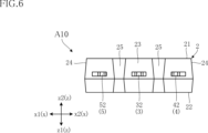
- FIG. 6 is a front view showing the semiconductor device according to the first embodiment.
- FIG. 7 is a bottom view showing the semiconductor device according to the first embodiment.
- FIG. 8 is a right side view showing the semiconductor device according to the first embodiment.
- FIG. 9 is a cross-sectional view taken along line IX-IX in FIG.
- FIG. 10 is a partially enlarged cross-sectional view of a part of FIG.
- FIG. 11 is a partially enlarged cross-sectional view of a part of FIG.
- FIG. 12 is a cross-sectional view taken along line XII-XII in FIG.
- FIG. 13 is a cross-sectional view taken along line XIII-XIII in FIG.
- FIG. 14 is a cross-sectional view taken along line XIV-XIV in FIG. 4, with a number of connecting members omitted.
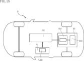
- FIG. 15 is a schematic diagram showing a vehicle including the semiconductor device according to the first embodiment.
- FIG. 15 is a schematic diagram showing a vehicle including the semiconductor device according to the first embodiment.
- FIG. 16 is a plan view showing a process for manufacturing the semiconductor device according to the first embodiment.
- FIG. 17 is a plan view showing a semiconductor device according to a first modification of the first embodiment.
- FIG. 18 is an enlarged view of a main part of a semiconductor device according to a second modification of the first embodiment, and corresponds to FIG.
- FIG. 19 is an enlarged view of a main part of a semiconductor device according to a third modification of the first embodiment, and corresponds to FIG.
- FIG. 20 is a plan view showing the semiconductor device according to the second embodiment, in which the sealing portion is shown by imaginary lines.
- FIG. 21 is a cross-sectional view showing the semiconductor device according to the second embodiment, taken along line XXI-XXI in FIG.
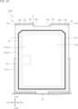
- FIG. 22 is a plan view showing a semiconductor device according to the third embodiment, in which a sealing portion is shown by an imaginary line.
- an object A is formed on an object B
- an object A is formed on (an object B)
- an object A is formed directly on an object B
- an object A is formed on an object B with another object interposed between the object A and the object B” unless otherwise specified.
- an object A is disposed on an object B” and “an object A is disposed on (an object B)” include “an object A is disposed directly on an object B” and “an object A is disposed on (an object B) with another object interposed between the object A and the object B” unless otherwise specified.
- an object A is located on (an object B)
- an object A is in contact with an object B and is located on (an object B)” and “an object A is located on (an object B) with another object interposed between the object A and the object B".
- an object A overlaps an object B includes “an object A overlaps the entirety of an object B” and “an object A overlaps a part of an object B” unless otherwise specified.
- An object A (its material) contains a certain material C includes “an object A (its material) is made of a certain material C” and "an object A (its material) mainly consists of a certain material C.”
- FIGS 1 to 4 show a semiconductor device A10 according to a first embodiment.
- the semiconductor device A10 comprises a semiconductor element 1, a conductive bonding material 19, a sealing portion 2, a plurality of leads 3, 4, 5, and a plurality of connecting members 61, 62.
- the semiconductor device A10 is a lead-through type TO (Transistor Outline) package.
- the package structure of the semiconductor device A10 is not limited to a TO package.
- the thickness direction z corresponds to the thickness direction of the semiconductor device A10.
- Planar view refers to the view in the thickness direction z.
- the z1 side of the thickness direction z is sometimes referred to as the bottom, and the z2 side of the thickness direction z is sometimes referred to as the top.
- Terms such as “top,” “bottom,” “upper,” “lower,” “top surface,” and “bottom surface” indicate the relative positional relationship of each component, etc. in the thickness direction z, and are not necessarily terms that define the relationship with the direction of gravity.
- the semiconductor element 1 is the functional core of the semiconductor device A10.
- the semiconductor element 1 is mounted on the lead 3.
- the semiconductor element 1 is, for example, a MOSFET (Metal-Oxide-Semiconductor Field-Effect Transistor).
- the semiconductor element 1 may be other transistors such as a bipolar transistor and an IGBT (Insulated Gate Bipolar Transistor), or may be a diode or an IC (Integrated Circuit) instead of a transistor.
- the semiconductor element 1 includes, for example, silicon (Si) or silicon carbide (SiC), but may also include other semiconductor materials (such as gallium nitride and diamond).
- the semiconductor element 1 has an element principal surface 10a and an element rear surface 10b.
- the element principal surface 10a and the element rear surface 10b are spaced apart from each other in the thickness direction z.
- the element principal surface 10a faces the z2 side in the thickness direction z (upward in the thickness direction z), and the element rear surface 10b faces the z1 side in the thickness direction z (downward in the thickness direction z).
- the element rear surface 10b faces the lead 3.
- the thickness of the semiconductor element 1 (dimension in the thickness direction z) is not limited in any way, but is, for example, 20 ⁇ m or more and 500 ⁇ m or less.
- the thickness of the semiconductor element 1 corresponds to the distance between the element principal surface 10a and the element rear surface 10b along the thickness direction z.
- the semiconductor element 1 has a first electrode 11, a second electrode 12, and a third electrode 13.
- the first electrode 11 is disposed on the back surface 10b of the element.
- the second electrode 12 and the third electrode 13 are each disposed on the main surface 10a of the element.
- the first electrode 11 and the second electrode 12 are switched between a conductive state and a cut-off state by a drive signal input to the third electrode 13.
- the semiconductor element 1 is a MOSFET
- the first electrode 11 is, for example, a drain electrode
- the second electrode 12 is, for example, a source electrode
- the third electrode 13 is, for example, a gate electrode.
- the conductive bonding material 19 bonds the semiconductor element 1. As shown in Figures 9 to 14, the conductive bonding material 19 is interposed between the semiconductor element 1 and the lead 3 (island 31 described below) and electrically bonds them together. In this embodiment, the element back surface 10b of the semiconductor element 1 faces the lead 3 (island 31 described below), so the conductive bonding material 19 electrically connects the first electrode 11 of the semiconductor element 1 to the lead 3 (island 31 described below).
- the conductive bonding material 19 is, for example, solder. Unlike this example, the conductive bonding material 19 may be a metal paste (for example, silver paste) or a sintered metal (for example, sintered silver).
- the sealing portion 2 covers the semiconductor element 1.
- the sealing portion 2 covers the conductive bonding material 19, portions of each of the multiple leads 3, 4, and 5, and the multiple connection members 61 and 62.
- the sealing portion 2 contains an electrically insulating resin material.
- the resin material is not limited to any particular material, but is, for example, epoxy resin.
- the method of forming the sealing portion 2 is not limited to any particular material, but is, for example, mold molding (insert molding).
- the sealing portion 2 has a resin main surface 21, a resin back surface 22, multiple resin side surfaces 23 and 24, and multiple recesses 25 and 26.
- the resin main surface 21 and the resin back surface 22 are spaced apart from each other in the thickness direction z.
- the resin main surface 21 faces the z2 side of the thickness direction z (upward in the thickness direction z), and the resin back surface 22 faces the z1 side of the thickness direction z (downward in the thickness direction z).
- the resin main surface 21 faces the same direction as the element main surface 10a in the thickness direction z, and the resin back surface 22 faces the same direction as the element back surface 10b in the thickness direction z.
- the thickness of the sealing portion 2 (dimension in the thickness direction z) is not limited in any way, but is, for example, 250 ⁇ m or more and 7 mm or less.
- the thickness of the sealing portion 2 corresponds to the distance between the resin main surface 21 and the resin back surface 22 in the thickness direction z.
- the pair of resin side surfaces 23 are spaced apart from each other in the first direction y and face opposite directions.
- the pair of resin side surfaces 23 are connected to the resin main surface 21 and the resin back surface 22.
- each of the multiple leads 3 to 5 protrudes from one of the pair of resin side surfaces 23 (the resin side surface 23 on the y1 side in the first direction y).
- the pair of resin side surfaces 24 are spaced apart from each other in the second direction x and face opposite directions.
- the pair of resin side surfaces 24 are connected to the resin main surface 21 and the resin back surface 22.
- each of the multiple recesses 25 is formed on one of the pair of resin side surfaces 23 (the resin side surface 23 on the y1 side in the first direction y). Each of the multiple recesses 25 is recessed from the resin side surface 23.
- the multiple recesses 25 include one formed between the two leads 3, 4 and one formed between the two leads 3, 5 in the second direction x.
- the multiple recesses 25 can increase the creepage distance along the resin side surface 23 for two adjacent leads out of the multiple leads 3 to 5.
- the sealing portion 2 may not include any of the multiple recesses 25.
- the multiple recesses 26 are recessed from the resin main surface 21 in the thickness direction z, and each individually connects from the resin side surface 23 on the y2 side of the first direction y to a pair of resin side surfaces 24.
- a portion of the lead 3 (an extension portion 34 and a portion of the island 31, which will be described later) is exposed from the multiple recesses 26.
- the sealing portion 2 may not include any of the multiple recesses 26.
- the multiple leads 3-5 form a conductive path between the semiconductor element 1 and a circuit board (not shown) on which the semiconductor device A10 is mounted.
- the multiple leads 3-5 are formed, for example, from the same lead frame.
- the lead frame is copper (Cu) or a copper alloy. Therefore, the composition of each of the multiple leads 3-5 includes copper.
- Each of the multiple leads 3-5 (lead frame) may include a metal other than copper.
- the multiple leads 3-5 are spaced apart from each other.
- Each of the multiple leads 3-5 protrudes from one of a pair of resin side surfaces 23 (the resin side surface 23 on the y1 side in the first direction y) as shown in Figures 3, 4, 6, and 7.
- the lead 3 has the semiconductor element 1 mounted thereon and is electrically connected to the first electrode 11 of the semiconductor element 1. As shown in Figures 4 and 5, the lead 3 includes an island 31, a terminal portion 32, a relay portion 33, and two extension portions 34. In the illustrated example, the lead 3 includes two extension portions 34, but may include three or more extension portions 34. In the lead 3, the island 31, the terminal portion 32, the relay portion 33, and the two extension portions 34 are integrally formed.
- the semiconductor element 1 is mounted on the island 31.
- the island 31 is, for example, rectangular in plan view. Therefore, the periphery 31c of the island 31 is rectangular in plan view. For ease of understanding, the periphery 31c is shown by a thick dashed line in FIG. 5.
- the island 31 includes a base 311 and an outer periphery 312.
- the base 311 overlaps the semiconductor element 1 in a plan view.
- the base 311 has a rectangular shape in a plan view.
- the thickness t311 of the base 311 is not limited in any way, but is, for example, 100 ⁇ m or more and 5 mm or less.
- the outer peripheral portion 312 is disposed around the base 311 in a plan view and surrounds the base 311.
- the outer peripheral portion 312 is rectangular annular in a plan view.
- the outer peripheral portion 312 does not overlap the semiconductor element 1 in a plan view. Unlike this example, a portion of the semiconductor element 1 may overlap the outer peripheral portion 312 in a plan view.
- the outer peripheral portion 312 includes a thin-walled portion 313.
- the thin portion 313 is covered by the sealing portion 2.
- the thin portion 313 is thinner than the base portion 311 and the outer peripheral portion 312 other than the thin portion 313. Therefore, the thickness t313 (dimension in the thickness direction z) of the thin portion 313 is smaller than the thickness t311 (dimension in the thickness direction z) of the base portion 311.
- the thickness t313 of the thin portion 313 is, for example, 15% to 20% of the thickness t311 of the base portion 311.
- the thickness t313 of the thin portion 313 is, for example, 100 ⁇ m to 4.9 mm. As shown in FIGS.
- the thin portion 313 includes, for example, a portion extending along the edge of the outer peripheral portion 312 on the y1 side in the first direction y, and a pair of portions connected to both ends of the portion in the second direction x and extending along the edge in the second direction x.
- the thin-walled portion 313 may be formed only on either one of the edges of the outer peripheral portion 312 in the first direction y or the edges of the outer peripheral portion 312 in the second direction x, or may be formed around the entire circumference of the outer peripheral portion 312.
- the thin-walled portion 313 is not limited to being continuous (see Figures 5 and 7), and may be divided into multiple portions. It is preferable that the thin-walled portion 313 does not overlap the semiconductor element 1 in a plan view, but it may overlap.
- the thin portion 313 includes a protrusion 313a.
- the protrusion 313a protrudes outward in a plan view.
- the protrusion 313a is formed on the z1 side of the thin portion 313 in the thickness direction z.
- the thin portion 313 is formed by crushing a part of the outer periphery 312, and the protrusion 313a is a part of this crushed part that protrudes outward.
- the thin portion 313 may not include the protrusion 313a.
- the island 31 has an island main surface 31a and an island back surface 31b.
- the island main surface 31a and the island back surface 31b are spaced apart from each other in the thickness direction z.
- the island main surface 31a faces the z2 side (upward in the thickness direction z) in the thickness direction z
- the island back surface 31b faces the z1 side (downward in the thickness direction z) in the thickness direction z.
- the island main surface 31a corresponds to the upper surface of the base 311 (surface facing the z2 side in the thickness direction z) and the upper surface of the outer peripheral portion 312 (surface facing the z2 side in the thickness direction z).
- the island back surface 31b corresponds to the lower surface of the base 311 (surface facing the z2 side in the thickness direction z) and the lower surface of the outer peripheral portion 312 excluding the thin portion 313 (surface facing the z1 side in the thickness direction z).
- the semiconductor element 1 is mounted on the island main surface 31a.
- the island back surface 31b is exposed from the resin back surface 22.
- the island back surface 31b is flush with the resin back surface 22.
- the thickness t311 of the base 311 corresponds to the distance along the thickness direction z from the island main surface 31a to the island back surface 31b.
- the terminal portion 32 is exposed from the sealing portion 2.
- the terminal portion 32 is a terminal of the semiconductor device A10, and is joined to the circuit board when the semiconductor device A10 is mounted on the circuit board.
- the terminal portion 32 is a portion of the lead 3 that protrudes from the resin side surface 23 of the sealing portion 2.
- the terminal portion 32 is separated from the island 31.
- the terminal portion 32 is located on the y1 side of the island 31 in the first direction y.
- the terminal portion 32 is located on the z2 side of the island 31 in the thickness direction z.
- the terminal portion 32 is an example of a "first terminal portion.”
- the relay portion 33 is connected to the island 31 and the terminal portion 32.
- the relay portion 33 is interposed between the island 31 and the terminal portion 32.
- the relay portion 33 is covered by the sealing portion 2.
- a part of the relay portion 33 is bent. This connects the island 31 and the terminal portion 32 that are arranged at different positions in the thickness direction z.
- the relay portion 33 is an example of a "first relay portion.”
- the lead 3 does not need to include the relay portion 33.
- the island 31 and the terminal portion 32 are electrically connected by a conductive member (e.g., a metal plate or a bonding wire).
- the two extension portions 34 each extend outward from the periphery 31c of the island 31.
- the two extension portions 34 each extend from the edge of the periphery 31c of the island 31 on the y2 side in the first direction y to the y2 side in the first direction y.
- the two extension portions 34 are each connected to the island 31 and formed integrally with it.
- the two extension portions 34 are each rectangular in a planar view, but the planar view shape of each extension portion 34 is not limited in any way.
- the two extension portions 34 are spaced apart from each other.
- the two extension portions 34 are arranged along the second direction x.
- the three or more extension portions 34 are arranged spaced apart from each other along the second direction x.
- the two extensions 34 are connected to a pair of corners 31d on the edge 31c of the island 31 that are farther from the terminal portion 32 in the first direction y.
- the two extensions 34 do not overlap the semiconductor element 1 and the conductive bonding material 19 in a plan view.
- each of the two extension portions 34 has an extension main surface 34a, an extension back surface 34b, and multiple extension side surfaces 34c and 34d.
- the extended main surface 34a and the extended back surface 34b are spaced apart from each other in the thickness direction z.
- the extended main surface 34a and the extended back surface 34b face opposite each other in the thickness direction z.
- the extended main surface 34a faces the z2 side in the thickness direction z (upward in the thickness direction z), and the extended back surface 34b faces the z1 side in the thickness direction z (downward in the thickness direction z).
- the extended main surface 34a is flush with the island main surface 31a.
- the extended back surface 34b is located on the z2 side in the thickness direction z of the island back surface 31b.
- a portion of the extended main surface 34a is exposed from the sealing portion 2 due to the recess 26, but the entire extended main surface 34a may be covered by the sealing portion 2.
- the extended back surface 34b is covered by the sealing portion 2.
- Each of the multiple extending side surfaces 34c, 34d is located between the extending main surface 34a and the extending back surface 34b in the thickness direction z. Each of the multiple extending side surfaces 34c, 34d extends from the extending main surface 34a to the z1 side in the thickness direction z.
- the extending side surface 34c faces the extending direction in which the extending portion 34 extends relative to the island 31 (in this embodiment, the y2 side of the first direction y).
- the extending side surface 34c is sandwiched between a pair of extending side surfaces 34d in the second direction x.
- the pair of extending side surfaces 34d are individually connected to both end edges of the extending side surface 34c in the thickness direction and in a direction perpendicular to the aforementioned extending direction.
- the pair of extending side surfaces 34d are spaced apart from each other in the second direction x and face opposite sides to each other in the second direction x.
- the pair of extending side surfaces 34d are each connected to the extending main surface 34a and the extending back surface 34b.
- Each of the multiple extending side surfaces 34c, 34d is covered with a sealing portion 2.
- the thickness t34 (dimension in thickness direction z) of each extension portion 34 is smaller than the thickness of the island 31 (thickness t311 of the base 311). As shown in FIG. 10, the thickness t34 of each extension portion 34 corresponds to the distance along the thickness direction z from the extension main surface 34a to the extension back surface 34b. The thickness t34 of each extension portion 34 is smaller than the thickness t313 of the thin portion 313.
- the thickness t34 of each extension portion 34 is not limited in any way, but is 15% or more and 75% or less of the thickness t311 of the base 311. In one example, the thickness t34 of each extension portion 34 is 50 ⁇ m or more and 4.8 mm or less.
- each of the two extension portions 34 includes a protrusion 341.
- the protrusion 341 described below is common to each extension portion 34 unless otherwise specified.
- the protrusion 341 protrudes outward from the island 31 in a plan view.
- the protrusion 341 protrudes from the extending side surface 34c of the corresponding extending portion 34 toward the y2 side in the first direction y.
- the protrusion 341 is formed at the end of the extending side surface 34c of the corresponding extending portion 34 on the z1 side in the thickness direction z.
- each extending portion 34 initially has the same thickness as the base 311. Then, by crushing each extending portion 34 having the same thickness as the base 311, each extending portion 34 becomes thinner than the base 311. The protrusion 341 is a part of this crushed portion protruding outward.
- each extending portion 34 may not include the protrusion 341.
- the protrusion 341 may be formed on the end of the extension side surface 34c of the corresponding extension portion 34 on the z1 side in the thickness direction z as well as on the z2 side in the thickness direction z.
- the width w34 of each extension portion 34 shown in FIG. 5 may be the same as the width w313 of the thin portion 313 shown in FIG. 5, or may be different. In this embodiment, the width w34 of each extension portion 34 is the dimension of the extension main surface 34a in the first direction y.
- the width w313 of the thin portion 313 and the width w34 of each extension portion 34 are not limited in any way, but in one example, the width w34 of each extension portion 34 is 100 ⁇ m or more and 1.5 mm or less, and in one example, the width w313 of the thin portion 313 is 100 ⁇ m or more and 1 mm or less.
- the inventor's research has revealed the following.
- increasing the width w313 of the thin portion 313 reduces the area of the island back surface 31b, which causes a decrease in heat dissipation.
- Increasing the width w313 of the thin portion 313 reduces the planar size of the base 311, which inhibits the expansion of the planar size of the semiconductor element 1. Therefore, there is a limit to how large the width w313 of the thin portion 313 can be.
- the width w34 of each extension 34 is increased, the area of the island back surface 31b does not decrease, so the heat dissipation performance is hardly reduced. Even if the width w34 of each extension 34 is increased, the planar size of the base 311 does not decrease, so there is no effect on the enlargement of the planar size of the semiconductor element 1.
- the width w34 of each extension 34 it is possible to reduce the stress applied to each extension 34 while suppressing the deterioration of heat dissipation.
- the width w34 of each extension 34 is increased, the product size (dimension in the first direction y) of the semiconductor device A10 increases. Therefore, the lower limit of the width w34 of each extension 34 is set in consideration of the thermal stress applied to each extension 34, and the upper limit is set according to the specifications of the semiconductor device A10 (dimension in the first direction y).
- the lead 4 is electrically connected to the second electrode 12 of the semiconductor element 1 via the connection member 61. As shown in FIG. 4, the lead 4 includes a pad portion 41, a terminal portion 42, and a relay portion 43. In the lead 4, the pad portion 41, the terminal portion 42, and the relay portion 43 are integrally formed.
- the pad portion 41 is covered by the sealing portion 2.
- a plurality of connection members 61 are each bonded to the pad portion 41.
- Each connection member 61 is bonded to the upper surface of the pad portion 41 (the surface facing the z2 side in the thickness direction z).
- the pad portion 41 is located on the z2 side in the thickness direction z of the island 31. In a plan view, the pad portion 41 is disposed on the y1 side of the island 31 in the first direction y.
- the terminal portion 42 is exposed from the sealing portion 2.
- the terminal portion 42 is a terminal of the semiconductor device A10, and is joined to the circuit board when the semiconductor device A10 is mounted on the circuit board.
- the terminal portion 42 is spaced apart from the pad portion 41.
- the terminal portion 42 is located on the y1 side of the pad portion 41 in the first direction y.
- the terminal portion 42 is disposed at the same position as the pad portion 41.
- the terminal portion 42 is located on the x2 side of the terminal portion 32 in the second direction x.
- the terminal portion 42 is disposed at the same position as the terminal portion 32.
- the terminal portion 42 is an example of a "second terminal portion.”
- the relay portion 43 is connected to the pad portion 41 and the terminal portion 42.
- the relay portion 43 is interposed between the pad portion 41 and the terminal portion 42.
- the relay portion 43 is covered by the sealing portion 2.
- a through hole is formed in the relay portion 43, but unlike this example, the relay portion 43 does not necessarily have to have a through hole. However, in a configuration in which a through hole is formed, the sealing portion 2 can move through the through hole when the sealing portion 2 is formed. By filling the through hole with the sealing portion 2, it is possible to prevent the lead 4 from coming out of the sealing portion 2.
- the relay portion 43 is an example of a "second relay portion".
- the lead 5 is electrically connected to the third electrode 13 of the semiconductor element 1 via the connection member 62. As shown in FIG. 4, the lead 5 includes a pad portion 51, a terminal portion 52, and a relay portion 53. In the lead 5, the pad portion 51, the terminal portion 52, and the relay portion 53 are integrally formed.
- the pad portion 51 is covered by the sealing portion 2.
- a connection member 62 is bonded to the pad portion 51.
- the connection member 62 is bonded to the upper surface of the pad portion 51 (the surface facing the z2 side in the thickness direction z).
- the pad portion 51 is located on the z2 side in the thickness direction z of the island 31. In a plan view, the pad portion 51 is disposed on the y1 side of the island 31 in the first direction y.
- the terminal portion 52 is exposed from the sealing portion 2.
- the terminal portion 52 is a terminal of the semiconductor device A10, and is joined to the circuit board when the semiconductor device A10 is mounted on the circuit board.
- the terminal portion 52 is a portion of the lead 5 that protrudes from the resin side surface 23 of the sealing portion 2.
- the terminal portion 52 is separated from the pad portion 51.
- the terminal portion 52 is located on the y1 side of the pad portion 51 in the first direction y. In the thickness direction z, the terminal portion 52 is arranged at the same position as the pad portion 51.
- the terminal portion 52 is arranged on the x1 side of the second direction x with respect to the terminal portion 32.
- the terminal portion 32 is arranged between the terminal portion 42 and the terminal portion 52.
- the arrangement order of the terminal portions 32, 42, and 52 in the second direction x is not limited to the illustrated example.
- the terminal portion 52 is arranged at the same position as the terminal portion 32. Therefore, in the thickness direction z, terminal portion 32, terminal portion 42, and terminal portion 52 are arranged at the same position as each other.
- the relay portion 53 is connected to the pad portion 51 and the terminal portion 52.
- the relay portion 53 is interposed between the pad portion 51 and the terminal portion 52.
- the relay portion 53 is covered by the sealing portion 2.
- a through hole is formed in the relay portion 53, but unlike this example, the relay portion 53 does not necessarily have to have a through hole.
- the sealing portion 2 can move through the through hole when the sealing portion 2 is formed. By filling the through hole with the sealing portion 2, it is possible to prevent the lead 5 from coming out of the sealing portion 2.
- the multiple connection members 61, 62 provide electrical conductivity between two parts spaced apart from each other.
- each of the multiple connection members 61, 62 is a bonding wire.
- the multiple connection members 61, 62 include a metal, and the metal is not limited to, but may be, for example, gold, aluminum, copper, silver, or an alloy containing these.
- Each of the multiple connection members 61, 62 may be a metal plate material instead of a bonding wire.
- connection members 61 are joined to the second electrode 12 and the pad portion 41, providing electrical continuity between them.
- the second electrode 12 is electrically connected to the lead 4 via the multiple connection members 61.
- the semiconductor device A10 has four connection members 61, but the number of connection members 61 is not limited in any way. It can be changed as appropriate depending on factors such as the magnitude of the current to be conducted between the second electrode 12 and the lead 4.
- connection member 62 is joined to the third electrode 13 and the pad portion 51, providing electrical continuity between them. Therefore, the third electrode 13 is electrically connected to the lead 5 via the connection member 62.
- the vehicle V is, for example, an electric vehicle (EV).
- EV electric vehicle
- the vehicle V includes an on-board charger 91, a storage battery 92, and a drive system 93.
- the on-board charger 91 is supplied with power wirelessly from a power supply facility (not shown) installed outdoors. Alternatively, the power supply from the power supply facility to the on-board charger 91 may be wired.
- the on-board charger 91 is configured with a step-up DC-DC converter.
- the semiconductor device A10 is part of the on-board charger 91, and is used, for example, in the DC-DC converter described above.
- the voltage of the power supplied to the on-board charger 91 is stepped up by the converter and then supplied to the storage battery 92.
- the stepped-up voltage is, for example, 600V.
- the drive system 93 drives the vehicle V.
- the drive system 93 has an inverter 931 and a drive source 932.
- the power stored in the storage battery 92 is supplied to the inverter 931.
- the power supplied from the storage battery 92 to the inverter 931 is DC power.
- a step-up DC-DC converter may be further provided between the storage battery 92 and the inverter 931.
- the inverter 931 converts DC power into AC power.
- the inverter 931 is conductive to the drive source 932.
- the drive source 932 has an AC motor and a transmission. When the AC power converted by the inverter 931 is supplied to the drive source 932, the AC motor rotates and the rotation is transmitted to the transmission.
- the transmission appropriately reduces the rotation speed transmitted from the AC motor and then rotates the drive shaft of the vehicle V. This drives the vehicle V.
- the inverter 931 is necessary to output AC power with an appropriate frequency change to correspond to the required rotation speed of the AC motor.
- the functions and effects of the semiconductor device A10 are as follows:
- the semiconductor device A10 includes an island 31 on which a semiconductor element 1 is mounted, and an extension 34 extending from the periphery 31c of the island 31.
- FIG. 16 shows a process in the manufacture of the semiconductor device A10, in which a number of leads 3 to 5 are connected to one another by tie bars 70 to form a single lead frame 7.
- the lead frame 7 is fixed by a clamp member. This is to suppress the swinging of the lead frame 7 due to vibrations that occur when the lead frame 7 is transported, when the semiconductor element 1 is bonded, when the lead frame 7 is bonded to the multiple connection members 61 and 62, and when the sealing portion 2 is formed.
- the clamp member can hold down the region R1 (shown by a dot pattern in FIG. 15).
- the extension 34 makes it possible to secure a location to be fixed by the clamp member, so that the range in which the clamp member interferes with the island 31 can be reduced. This also suppresses interference between the semiconductor element 1 and the clamping member, making it possible for the semiconductor device A10 to increase the planar size of the semiconductor element 1.
- the planar size of the semiconductor element 1 can be made the same (or approximately the same) as the planar size of the island 31.
- the multiple extending side surfaces 34c, 34d of each extending portion 34 are each covered by the sealing portion 2.
- This configuration allows the semiconductor device A10 to have an appearance that is the same (or approximately the same) as a conventional TO package. In other words, the semiconductor device A10 makes it possible to increase the planar size of the semiconductor element 1 without changing the appearance from the conventional one.
- the extended back surface 34b is covered by the sealing portion 2. This configuration makes it possible to prevent the lead 3 from coming out of the sealing portion 2.
- the thickness t34 of each extension portion 34 is smaller than the thickness t311 of the base 311 (corresponding to the thickness of the island 31).
- the extension main surface 34a of each extension portion 34 is flush with the island main surface 31a. In this configuration, even if the island back surface 31b is exposed from the resin back surface 22, the extension back surface 34b of each extension portion 34 is covered by the sealing portion 2. Therefore, the semiconductor device A10 can prevent the island 31 from coming out of the sealing portion 2.
- the outer peripheral portion 312 of the island 31 includes a thin portion 313.
- the thickness t313 of the thin portion 313 is smaller than the thickness t311 of the base portion 311.
- the lower surface of the thin portion 313 (the surface facing the z1 side in the thickness direction z) is covered with the sealing portion 2. This configuration makes it possible to prevent the island 31 from coming out of the sealing portion 2.
- the island back surface 31b is exposed from the sealing portion 2 (resin back surface 22). This configuration can improve the heat dissipation properties for the heat generated by the semiconductor element 1.
- each extension portion 34 does not overlap the semiconductor element 1 in a planar view.
- the semiconductor element 1 does not protrude from the island 31 in a planar view. Therefore, the semiconductor device A10 can suppress a decrease in the conduction area between the first electrode 11 of the semiconductor element 1 and the island 31.
- each extension 34 extends in the first direction y from the edge on the y2 side of the periphery 31c of the island 31.
- each extension 34 region R1 in FIG. 15
- the vicinity of the tie bar 70 region R2 in FIG. 15
- the points pressed by the clamp member can be separated in the first direction y, which is preferable in terms of suppressing oscillation of the lead frame 7.
- the semiconductor device A10 has two extending portions 34 spaced apart from each other. With this configuration, the two extending portions 34 (both of the two regions R1 in FIG. 15) are held down by the clamp member described above, and the vicinity of the tie bar 70 (at least one of the three regions R2 in FIG. 15) is held down, so that the lead frame 7 can be held down and fixed at three points. This can further suppress the swinging of the lead frame 7 during the manufacture of the semiconductor device A10.
- the two extending portions 34 are connected to a pair of corners 31d, which are far from the terminal portion 32 in the first direction y, of the periphery 31c of the island 31 as viewed in the thickness direction z. In this case, the planar area of the three points held down by the clamp member can be increased. This is preferable for fixing the lead frame 7, that is, for suppressing the swinging of the lead frame 7 during the manufacture of the semiconductor device A10.
- FIG. 17 shows a semiconductor device A11 according to a first modified example of the first embodiment.
- the semiconductor device A11 differs from the semiconductor device A10 in the following respect. That is, the semiconductor device A11 differs in that the sealing portion 2 does not include any of the multiple recesses 26.
- the sealing portion 2 does not include any of the multiple recesses 26, so the top surface of the island 31 (island main surface 31a) and the top surfaces of each extension portion 34 (extension main surface 34a) are all covered with the sealing portion 2. Therefore, all of the leads 3 of the semiconductor device A11 are covered with the sealing portion 2 except for the terminal portions 32, so unintended short circuits can be suppressed.
- the semiconductor device A11 Similar to the semiconductor device A10, the semiconductor device A11 includes an island 31 on which a semiconductor element 1 is mounted, and an extension portion 34 extending from a periphery 31c of the island 31. Therefore, similar to the semiconductor device A10, the semiconductor device A11 can suppress interference between the semiconductor element 1 and the clamp member, making it possible to increase the size of the semiconductor element 1 in a plan view. In addition, the semiconductor device A11 has a common configuration with the semiconductor device A10, and thus achieves the same effects as the semiconductor device A10.
- FIG. 18 shows a semiconductor device A12 according to a second modified example of the first embodiment.
- the semiconductor device A12 differs from the semiconductor device A10 in the following respect: the island 31 includes a groove portion 314.
- the groove 314 is recessed from the island main surface 31a.
- the groove 314 is, for example, rectangular and annular in plan view. In plan view, the groove 314 is formed along the boundary between the base 311 and the outer periphery 312. In plan view, the groove 314 surrounds the semiconductor element 1 and the conductive bonding material 19. This groove 314 can prevent the conductive bonding material 19 from flowing out. By filling the groove 314 with the sealing portion 2, the adhesion between the sealing portion 2 and the lead 3 is increased.
- the semiconductor device A12 Similar to the semiconductor device A10, the semiconductor device A12 includes an island 31 on which a semiconductor element 1 is mounted, and an extension portion 34 extending from the periphery 31c of the island 31. Therefore, similar to the semiconductor device A10, the semiconductor device A12 can suppress interference between the semiconductor element 1 and the clamp member, making it possible to increase the size of the semiconductor element 1 in a plan view. In addition, the semiconductor device A12 has a common configuration with the semiconductor devices A10 and A11, and thus achieves the same effects as the semiconductor devices A10 and A11.
- FIG. 19 shows a semiconductor device A13 according to a third modified example of the first embodiment.
- the semiconductor device A13 differs from the semiconductor device A10 in the following respect. That is, when viewed in the thickness direction z, the two extension portions 34 are not connected to a pair of corner portions 31d of the periphery 31c of the island 31 that are far from the terminal portion 32 in the first direction y.
- the extension 34 on the x1 side in the second direction x is disposed closer to the x2 side in the second direction x than the semiconductor device A10, and the extension 34 on the x2 side in the second direction x is disposed closer to the x1 side in the second direction x than the semiconductor device A10.
- the semiconductor device A13 Similar to the semiconductor device A10, the semiconductor device A13 includes an island 31 on which a semiconductor element 1 is mounted, and an extension portion 34 extending from the periphery 31c of the island 31. Therefore, similar to the semiconductor device A10, the semiconductor device A13 can suppress interference between the semiconductor element 1 and the clamp member, making it possible to increase the size of the semiconductor element 1 in a plan view. In addition, the semiconductor device A13 has a common configuration with each of the semiconductor devices A10 to A12, and thus achieves the same effects as the semiconductor devices A10 to A12.
- each extension portion 34 is connected to one of a pair of corner portions 31d of the periphery 31c of the island 31.
- FIGS. 20 and 21 show a semiconductor device A20 according to the second embodiment.
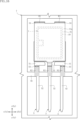
- the semiconductor device A20 differs from the semiconductor device A10 in the following respect. That is, two extension portions 34 extend in the second direction x individually from each end edge of the periphery 31c of the island 31 in the second direction x. For ease of understanding, the periphery 31c of the island 31 is shown by a thick dashed line in FIG. 20.
- one of the two extension portions 34 extends from the edge of peripheral edge 31c on the x1 side in the second direction x to the x1 side in the second direction x.
- the other of the two extension portions 34 extends from the edge of peripheral edge 31c on the x2 side in the second direction x to the x2 side in the second direction x.
- the two extension portions 34 of semiconductor device A20 are each connected to a pair of corner portions 31d of peripheral edge 31c of island 31.
- the two extensions 34 may not be connected to a pair of corners 31d of the periphery 31c of the island 31, but may be disposed at the center of each edge of the periphery 31c in the second direction x, or may be connected to a pair of corners of the periphery 31c of the island 31 on opposite sides from the terminal portion 32 in the first direction y.
- each extension 34 extends in the second direction x relative to the island 31, so that the extension side surface 34c of each extension 34 faces in one direction in the second direction x.
- the semiconductor device A20 includes an island 31 on which the semiconductor element 1 is mounted, and an extension portion 34 extending from the periphery 31c of the island 31. Therefore, similar to the semiconductor device A10, the semiconductor device A20 can suppress interference between the semiconductor element 1 and the clamp member, making it possible to increase the size of the semiconductor element 1 in a plan view. In addition, the semiconductor device A20 has a common configuration with each of the semiconductor devices A10 to A13, and thus achieves the same effects as the semiconductor devices A10 to A13.
- each extension portion 34 is not limited to extending from an edge of the periphery 31c of the island 31 in the first direction y, but may extend from an edge in the second direction x. Furthermore, in the semiconductor device of the present disclosure, the multiple extension portions 34 only need to extend from the periphery 31c of the island 31 outward from the island 31, and the arrangement of the multiple extension portions 34 is not limited in any way.
- the multiple extension portions 34 may include a mixture of those extending from an edge of the periphery 31c in the first direction y and those extending from an edge in the second direction x.
- FIG. 22 shows a semiconductor device A30 according to the third embodiment.
- the semiconductor device A30 differs from the semiconductor device A10 in the following respect: the number of extension portions 34 is one.
- the lead 3 of the semiconductor device A30 includes one extension portion 34.
- the periphery 31c of the island 31 is shown by a thick dashed line in FIG. 21.
- the extension 34 extends from the edge of the periphery 31c of the island 31 on the y2 side in the first direction y.
- the extension 34 may extend from the edge of the periphery 31c on the x1 side in the second direction x, or from the edge of the periphery 31c on the x2 side in the second direction x.
- the semiconductor device A30 includes an island 31 on which a semiconductor element 1 is mounted, and an extension portion 34 extending from the periphery 31c of the island 31. Therefore, similar to the semiconductor device A10, the semiconductor device A30 can suppress interference between the semiconductor element 1 and the clamp member, making it possible to increase the size of the semiconductor element 1 in a plan view.
- the semiconductor device A30 has a common configuration with the semiconductor devices A10 to A13, A20, and thus achieves the same effects as the semiconductor devices A10 to A13, A20.
- the number of extension portions 34 may be one or more.
- the semiconductor device according to the present disclosure is not limited to the above-mentioned embodiment.
- the specific configuration of each part of the semiconductor device according to the present disclosure can be freely designed in various ways.
- the semiconductor device according to the present disclosure includes the embodiments described in the following appendix. Appendix 1.
- a semiconductor element an island on which the semiconductor element is mounted; At least one extension portion extending from a periphery of the island when viewed in a thickness direction of the island; a sealing portion for covering the semiconductor element; Equipped with The at least one extension portion has an extension main surface facing one side in the thickness direction, an extension back surface facing the opposite side to the extension main surface in the thickness direction, and an extension side surface arranged between the extension main surface and the extension back surface in the thickness direction, The extending side surface is covered by the sealing portion.
- the island includes a base portion at least a portion of which overlaps with the semiconductor element when viewed in the thickness direction, and an outer periphery portion surrounding the base portion when viewed in the thickness direction, 2.
- the outer periphery includes a thin-walled portion whose dimension in the thickness direction is smaller than the dimension in the thickness direction of the base.
- Appendix 3. The semiconductor device according to claim 2, wherein a dimension in the thickness direction of the at least one extension portion is smaller than a dimension in the thickness direction of the thin portion.
- Appendix 4. the island has an island main surface on which the semiconductor element is mounted, the island main surface facing in the same direction as the extended main surface in the thickness direction; 4.
- the semiconductor device according to claim 1, wherein the island main surface and the extended main surface are flush with each other.
- Appendix 5. 5 The semiconductor device according to claim 4, wherein a dimension of the at least one extension in the thickness direction is smaller than a dimension of the island in the thickness direction.
- Appendix 6 The semiconductor device according to claim 5, wherein the extended back surface is covered by the sealing portion.
- Appendix 7. the island has an island back surface facing a side opposite to the island main surface in the thickness direction, 7.
- the at least one extension portion includes a plurality of extension portions, 8.
- the semiconductor device according to claim 1, wherein the plurality of extension portions are spaced apart from each other.
- Appendix 9. 9.
- the semiconductor device according to claim 1, wherein the at least one extending portion does not overlap the semiconductor element when viewed in the thickness direction.
- Appendix 10. a first terminal portion spaced apart from the island and exposed from the sealing portion; 10.
- the semiconductor device wherein the first terminal portion is electrically connected to the semiconductor element.
- Appendix 11. The semiconductor device according to claim 10, wherein the first terminal portion is located on one side of the island in a first direction perpendicular to the thickness direction when viewed in the thickness direction.
- Appendix 12. The semiconductor device according to claim 11, wherein the at least one extension portion extends from an edge of the island opposite the first terminal portion in the first direction when viewed in the thickness direction.
- Appendix 13 12.
- the semiconductor device wherein the at least one extension portion extends from an edge of the island in a second direction perpendicular to the thickness direction and the first direction when viewed in the thickness direction.
- Appendix 14. The island has a rectangular shape when viewed in the thickness direction, 14.
- the semiconductor device wherein the at least one extension portion is connected to a corner portion of the island that is farthest from the first terminal portion in the first direction when viewed in the thickness direction.
- Appendix 15. a second terminal portion spaced apart from the island and the first terminal portion and exposed from the sealing portion; 15. The semiconductor device according to claim 10, wherein the second terminal is electrically connected to the semiconductor element.
- Appendix 16. A connection member joined to the semiconductor element; A pad portion to which the connection member is joined, 16. The semiconductor device according to claim 15, wherein the second terminal portion is electrically connected to the semiconductor element via the connection member and the pad portion.
- Appendix 17. a first relay portion connected to each of the first terminal portion and the island and integrally formed with each of the first terminal portion and the island; 17.
- the semiconductor device further comprising: a second relay portion connected to each of the second terminal portion and the pad portion and integrally formed with each of the second terminal portion and the pad portion.
- Appendix 18 A driving source; A storage battery that stores power to be supplied to the driving source; an on-board charger that converts power input from an external source and supplies the power to the storage battery; Equipped with 18.
Landscapes
- Structures Or Materials For Encapsulating Or Coating Semiconductor Devices Or Solid State Devices (AREA)
Priority Applications (1)
| Application Number | Priority Date | Filing Date | Title |
|---|---|---|---|
| JP2025518117A JPWO2024228322A1 (https=) | 2023-05-01 | 2024-04-11 |
Applications Claiming Priority (2)
| Application Number | Priority Date | Filing Date | Title |
|---|---|---|---|
| JP2023-075727 | 2023-05-01 | ||
| JP2023075727 | 2023-05-01 |
Publications (1)
| Publication Number | Publication Date |
|---|---|
| WO2024228322A1 true WO2024228322A1 (ja) | 2024-11-07 |
Family
ID=93333028
Family Applications (1)
| Application Number | Title | Priority Date | Filing Date |
|---|---|---|---|
| PCT/JP2024/014632 Ceased WO2024228322A1 (ja) | 2023-05-01 | 2024-04-11 | 半導体装置 |
Country Status (2)
| Country | Link |
|---|---|
| JP (1) | JPWO2024228322A1 (https=) |
| WO (1) | WO2024228322A1 (https=) |
Citations (2)
| Publication number | Priority date | Publication date | Assignee | Title |
|---|---|---|---|---|
| JPH08139253A (ja) * | 1994-11-11 | 1996-05-31 | Sanyo Electric Co Ltd | リードフレームと半導体装置の製造方法 |
| JP2017135241A (ja) * | 2016-01-27 | 2017-08-03 | ローム株式会社 | 半導体装置 |
-
2024
- 2024-04-11 JP JP2025518117A patent/JPWO2024228322A1/ja active Pending
- 2024-04-11 WO PCT/JP2024/014632 patent/WO2024228322A1/ja not_active Ceased
Patent Citations (2)
| Publication number | Priority date | Publication date | Assignee | Title |
|---|---|---|---|---|
| JPH08139253A (ja) * | 1994-11-11 | 1996-05-31 | Sanyo Electric Co Ltd | リードフレームと半導体装置の製造方法 |
| JP2017135241A (ja) * | 2016-01-27 | 2017-08-03 | ローム株式会社 | 半導体装置 |
Also Published As
| Publication number | Publication date |
|---|---|
| JPWO2024228322A1 (https=) | 2024-11-07 |
Similar Documents
| Publication | Publication Date | Title |
|---|---|---|
| JP5232367B2 (ja) | 半導体装置 | |
| US10056309B2 (en) | Electronic device | |
| CN106158839B (zh) | 半导体器件 | |
| US8373197B2 (en) | Circuit device | |
| WO2016185666A1 (ja) | 半導体装置 | |
| WO2022138068A1 (ja) | 半導体パッケージおよびこれを用いた電子装置 | |
| JP6354674B2 (ja) | 半導体装置 | |
| WO2021002132A1 (ja) | 半導体モジュールの回路構造 | |
| WO2022264733A1 (ja) | 半導体装置 | |
| US20250372511A1 (en) | Semiconductor device and vehicle | |
| US20220102253A1 (en) | Semiconductor package and method of manufacturing a semiconductor package | |
| WO2024228322A1 (ja) | 半導体装置 | |
| WO2024176740A1 (ja) | 半導体装置および車両 | |
| JP7512659B2 (ja) | 半導体モジュール及び半導体モジュールの製造方法 | |
| JP2023134143A (ja) | 半導体モジュール、半導体装置、及び車両 | |
| US12500185B2 (en) | Semiconductor device | |
| US20260060119A1 (en) | Semiconductor device | |
| JP7845458B2 (ja) | 金属配線板 | |
| US20260076183A1 (en) | Electronic device | |
| JP7546783B2 (ja) | 半導体装置、電力変換装置、および、半導体装置の製造方法 | |
| US20240429147A1 (en) | Semiconductor apparatus | |
| JP2024175866A (ja) | 半導体装置、半導体装置の製造方法、および車両 | |
| JP2025118106A (ja) | 半導体装置 | |
| CN117199011A (zh) | 半导体模块以及半导体模块的制造方法 | |
| JP2023180199A (ja) | 半導体モジュールおよび半導体モジュールの製造方法 |
Legal Events
| Date | Code | Title | Description |
|---|---|---|---|
| 121 | Ep: the epo has been informed by wipo that ep was designated in this application |
Ref document number: 24800053 Country of ref document: EP Kind code of ref document: A1 |
|
| ENP | Entry into the national phase |
Ref document number: 2025518117 Country of ref document: JP Kind code of ref document: A |
|
| WWE | Wipo information: entry into national phase |
Ref document number: 2025518117 Country of ref document: JP |
|
| NENP | Non-entry into the national phase |
Ref country code: DE |