WO2024219005A1 - 計測装置、計測方法、及び加工装置 - Google Patents
計測装置、計測方法、及び加工装置 Download PDFInfo
- Publication number
- WO2024219005A1 WO2024219005A1 PCT/JP2023/043915 JP2023043915W WO2024219005A1 WO 2024219005 A1 WO2024219005 A1 WO 2024219005A1 JP 2023043915 W JP2023043915 W JP 2023043915W WO 2024219005 A1 WO2024219005 A1 WO 2024219005A1
- Authority
- WO
- WIPO (PCT)
- Prior art keywords
- light
- laser light
- detection unit
- inspection
- processing
- Prior art date
- Legal status (The legal status is an assumption and is not a legal conclusion. Google has not performed a legal analysis and makes no representation as to the accuracy of the status listed.)
- Ceased
Links
Images




Classifications
-
- G—PHYSICS
- G01—MEASURING; TESTING
- G01B—MEASURING LENGTH, THICKNESS OR SIMILAR LINEAR DIMENSIONS; MEASURING ANGLES; MEASURING AREAS; MEASURING IRREGULARITIES OF SURFACES OR CONTOURS
- G01B11/00—Measuring arrangements characterised by the use of optical techniques
- G01B11/30—Measuring arrangements characterised by the use of optical techniques for measuring roughness or irregularity of surfaces
-
- B—PERFORMING OPERATIONS; TRANSPORTING
- B23—MACHINE TOOLS; METAL-WORKING NOT OTHERWISE PROVIDED FOR
- B23K—SOLDERING OR UNSOLDERING; WELDING; CLADDING OR PLATING BY SOLDERING OR WELDING; CUTTING BY APPLYING HEAT LOCALLY, e.g. FLAME CUTTING; WORKING BY LASER BEAM
- B23K26/00—Working by laser beam, e.g. welding, cutting or boring
- B23K26/352—Working by laser beam, e.g. welding, cutting or boring for surface treatment
-
- B—PERFORMING OPERATIONS; TRANSPORTING
- B23—MACHINE TOOLS; METAL-WORKING NOT OTHERWISE PROVIDED FOR
- B23K—SOLDERING OR UNSOLDERING; WELDING; CLADDING OR PLATING BY SOLDERING OR WELDING; CUTTING BY APPLYING HEAT LOCALLY, e.g. FLAME CUTTING; WORKING BY LASER BEAM
- B23K26/00—Working by laser beam, e.g. welding, cutting or boring
- B23K26/352—Working by laser beam, e.g. welding, cutting or boring for surface treatment
- B23K26/354—Working by laser beam, e.g. welding, cutting or boring for surface treatment by melting
-
- G—PHYSICS
- G01—MEASURING; TESTING
- G01N—INVESTIGATING OR ANALYSING MATERIALS BY DETERMINING THEIR CHEMICAL OR PHYSICAL PROPERTIES
- G01N21/00—Investigating or analysing materials by the use of optical means, i.e. using sub-millimetre waves, infrared, visible or ultraviolet light
- G01N21/17—Systems in which incident light is modified in accordance with the properties of the material investigated
- G01N21/47—Scattering, i.e. diffuse reflection
Definitions
- This disclosure relates to a measuring device, a measuring method, and a processing device.
- laser polishing has become known, in which the surface of an object is smoothed by irradiating it with laser light.
- the surface of the object is smoothed by melting and rearranging the surface material or by ablation using laser light.
- laser polishing has the advantages of being able to process any area of an object with a complex shape, minimizing changes in the shape of the object before and after processing, and not producing any polishing debris, and further development of the technology is desirable.
- Patent Document 1 As an example of a method for measuring the surface condition of an object using light instead of a microscope, there is the surface defect detection device described in Patent Document 1.
- an inspection laser beam is incident on the surface of the object at an angle, and the scattered light and specularly reflected light from the surface of the object are measured by a light receiving element. Then, defects on the surface of the object are detected based on the ratio of the intensity of the scattered light to the intensity of the specularly reflected light.
- the present disclosure has been made to solve the above problems, and aims to provide a measuring device, a measuring method, and a processing device using the same that are suitable for real-time measurement of the surface roughness of an object during laser polishing.
- a measuring device for measuring the surface roughness of an object, and includes an inspection light source that outputs inspection laser light to the surface of the object, a first detection unit that detects specularly reflected light of the inspection laser light from a measurement point on the surface of the object, a second detection unit that detects scattered light of the inspection laser light from the measurement point on the surface of the object, and an off-axis parabolic mirror element having a first surface, a second surface that is configured with a concave parabolic mirror surface and is located opposite the first surface, and a through hole that connects the first surface and the second surface, and the off-axis parabolic mirror element is arranged so that the inspection laser light from the inspection light source travels from the first surface side through the through hole to the object, the specularly reflected light that has passed through the through hole from the second surface side travels to the first detection unit, and the scattered light reflected by the second surface travels to the second detection unit.
- the arrangement of the off-axis parabolic mirror element allows the detection of the specularly reflected light in the first detecting section and the detection of the scattered light in the second detecting section to be performed simultaneously.
- the scattered light generated on the surface of the object proceeds to the second detecting section at a certain solid angle by the second surface of the off-axis parabolic mirror element, which is a concave parabolic mirror surface. Therefore, even if the surface of the object is a polished surface and the scattered light is anisotropic, or even if the surface of the object is a smooth surface and the scattered light is weak, the scattered light can be detected with sufficient intensity in the second detecting section.
- the through hole of the off-axis parabolic mirror element functions as an aperture that passes only the specularly reflected light, and light other than the specularly reflected light can be prevented from proceeding to the first detecting section, and the scattered light reflected by the second surface can be shifted spatially or temporally relative to the processing laser light, thereby preventing the emission of plasma generated on the surface of the object by irradiation with the processing laser light from proceeding to the second detecting section together with the scattered light. Therefore, this measuring device can be used to ideally perform real-time measurement of the surface roughness of objects during laser polishing.
- the measuring device may further include a calculation unit that calculates the surface roughness of the object based on the ratio between the intensity of the specularly reflected light detected by the first detection unit and the intensity of the scattered light detected by the second detection unit.
- a calculation unit that calculates the surface roughness of the object based on the ratio between the intensity of the specularly reflected light detected by the first detection unit and the intensity of the scattered light detected by the second detection unit.
- the off-axis parabolic mirror element may be arranged so that the inspection laser light from the inspection light source travels perpendicular to the surface of the object through the through hole from the first surface side. If the inspection laser light travels obliquely to the surface of the object, it is conceivable that if the height of the object shifts, the optical path of the specularly reflected light will shift significantly and will no longer travel to the first detection unit. By arranging the off-axis parabolic mirror element so that the inspection laser light travels perpendicular to the surface of the object, the optical path of the specularly reflected light is maintained even if the height of the object shifts, so the measurement accuracy of the surface roughness can be guaranteed.
- the through hole may be gradually narrowed from the first surface side toward the second surface side. This enhances the aperture function of the through hole, and more reliably prevents scattered light or plasma emission caused by the processing laser light from progressing to the first detection section. This further improves the measurement accuracy of the surface roughness.
- the measuring device may further include a focusing lens disposed in the optical path of the scattered light between the second surface and the second detection unit. This allows the detection intensity of the scattered light at the second detection unit to be further increased. This further improves the measurement accuracy of the surface roughness.
- the measurement device may further include a half mirror that shares a portion of the optical path of the inspection laser light between the inspection light source and the first surface, and a portion of the optical path of the specularly reflected light between the first surface and the first detection unit. In this case, sharing a portion of the optical path of the inspection laser light and the optical path of the specularly reflected light allows the device to be made more compact.
- the measuring device may have an adjustment mechanism that adjusts the relative positional relationship between the object and the off-axis parabolic mirror element in the direction of propagation of the inspection laser light from the first surface side through the through hole toward the object.
- Such an adjustment mechanism makes it easy to align the object and the off-axis parabolic mirror element.
- the adjustment mechanism may be configured with a holding part that holds the off-axis parabolic mirror element so that it can move freely in the direction of propagation of the inspection laser light that passes from the first surface side through the through hole toward the object. This makes it possible to easily adjust the distance between the off-axis parabolic mirror element and the surface of the object to the focal length of the second surface of the off-axis parabolic mirror element, which is a concave parabolic mirror surface, even when measuring objects of different heights.
- the adjustment mechanism may be composed of a stage that holds the object so that it can move freely in the direction of propagation of the inspection laser light that passes from the first surface side through the through hole toward the object. This makes it possible to easily adjust the distance between the off-axis parabolic mirror element and the surface of the object to the focal length of the second surface of the off-axis parabolic mirror element, which is a concave parabolic mirror surface, even when measuring objects of different heights.
- the first and second detection units may be configured with single-channel photodiodes.
- the information used for roughness measurement is only the intensity signals of specularly reflected light and scattered light. Therefore, the amount of data to be handled can be reduced compared to when roughness measurement is performed based on two-dimensional image processing, and processing speed can be increased.
- a measurement method is a measurement method for measuring the surface roughness of an object, and includes an output step of outputting an inspection laser light to the surface of the object, and a detection step of detecting the specularly reflected light of the inspection laser light from the measurement point on the surface of the object with a first detection unit and detecting the scattered light of the inspection laser light from the measurement point on the surface of the object with a second detection unit.
- an off-axis parabolic mirror element having a first surface, a second surface formed of a concave parabolic mirror surface and positioned opposite the first surface, and a through hole connecting the first surface and the second surface is used, and the off-axis parabolic mirror element is positioned so that the inspection laser light travels from the first surface side through the through hole to the object, the specularly reflected light that passes through the through hole from the second surface side travels to the first detection unit, and the scattered light reflected by the second surface travels to the second detection unit.
- the arrangement of the off-axis parabolic mirror element allows the detection of the specularly reflected light in the first detection unit and the detection of the scattered light in the second detection unit to be performed simultaneously.
- the scattered light generated on the surface of the object proceeds to the second detection unit at a certain solid angle by the second surface of the off-axis parabolic mirror element, which is a concave parabolic mirror surface. Therefore, even if the surface of the object is a polished surface and the scattered light is anisotropic, or even if the surface of the object is a smooth surface and the scattered light is weak, the scattered light can be detected with sufficient intensity in the second detection unit.
- the through hole of the off-axis parabolic mirror element functions as an aperture that passes only the specularly reflected light, and light other than the specularly reflected light can be prevented from proceeding to the first detection unit, and the scattered light reflected by the second surface can be shifted spatially or temporally relative to the processing laser light, thereby preventing the emission of plasma generated on the surface of the object by irradiation with the processing laser light from proceeding to the second detection unit together with the scattered light. Therefore, this measuring device can be used to ideally perform real-time measurement of the surface roughness of objects during laser polishing.
- the processing device is a processing device that processes the surface of an object, and includes a processing light source that outputs processing laser light to the surface of the object, and the above-mentioned measuring device.
- this processing device can suitably perform real-time measurement of the surface roughness of the object during laser polishing.
- the processing device may further include a calculation unit that calculates the surface roughness of the object based on the ratio between the intensity of the specularly reflected light detected by the first detection unit and the intensity of the scattered light detected by the second detection unit.
- a calculation unit that calculates the surface roughness of the object based on the ratio between the intensity of the specularly reflected light detected by the first detection unit and the intensity of the scattered light detected by the second detection unit.
- the processing device may further include a stage that holds the object so that it can move freely in the direction of travel of the inspection laser light that travels from the first surface side toward the object through the through hole, and in the in-plane direction of the object's surface.
- the processing laser light and the inspection laser light can be scanned over the object's surface by the stage. Therefore, the surface roughness of the object can be measured continuously along the processing area, improving the workability of processing.
- the irradiation position of the inspection laser light on the surface of the object may be shifted from the irradiation position of the processing laser light.
- the plasma light emission is prevented from entering the second detection unit, and the plasma light emission can be prevented from affecting the measurement of the surface roughness of the object.
- An aperture that passes only the scattered light may be disposed in the optical path of the scattered light between the second surface and the second detection unit. In this case, light other than the scattered light can be blocked by the aperture, so that the plasma emission caused by the processing laser light can be prevented from progressing to the second detection unit. This makes it possible to more effectively perform real-time measurement of the surface roughness of the object.
- the processing device may further include a control unit that controls the processing light source and the inspection light source so that the processing laser light and the inspection laser light are irradiated onto the surface of the object with different output periods.
- a control unit that controls the processing light source and the inspection light source so that the processing laser light and the inspection laser light are irradiated onto the surface of the object with different output periods.
- the calculation unit may calculate the surface roughness of the object based on the ratio between the intensity of the specularly reflected light detected by the first detection unit during a period when the processing laser light is not irradiated onto the surface of the object, and the intensity of the scattered light detected by the second detection unit during the same period. In this case, the influence of plasma light emission caused by the processing laser light can be eliminated when calculating the surface roughness of the object. This improves the measurement accuracy of the surface roughness.
- This disclosure makes it possible to effectively perform real-time measurement of the surface roughness of an object during laser polishing.
- FIG. 1 is a schematic diagram illustrating a configuration of a measurement device according to an embodiment of the present disclosure.
- FIG. 4 is a diagram showing an example of calibration curve data stored in a calculation unit.
- FIG. 2 is an enlarged view showing the configuration of an off-axis parabolic mirror element.
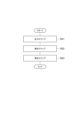
- 1 is a flowchart illustrating an example of a measurement method according to an embodiment of the present disclosure.
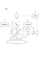
- 2 is a schematic diagram showing an example of the configuration of a processing apparatus including the measuring apparatus shown in FIG. 1 . 1.
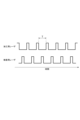
- FIG. 4 is a schematic diagram showing another example of the configuration of a processing apparatus including the measuring device shown in FIG. 7 is a diagram showing output timings of a processing laser beam and an inspection laser beam in the processing apparatus shown in FIG. 6 . 1.
- FIG. 4 is a schematic diagram showing yet another example of the configuration of a processing apparatus including the measuring device shown in FIG.
- FIG. 1 is a schematic diagram showing the configuration of a measurement device according to one embodiment of the present disclosure.
- the measurement device 1 shown in FIG. 1 is configured as a device for measuring the roughness of a surface Sa of an object S.
- the object S is not particularly limited, but may be, for example, various metal materials such as copper, aluminum, iron, etc., or a semiconductor wafer.
- the measurement device 1 includes a stage 2 on which the object S is placed, an inspection light source 3 that outputs an inspection laser light Ld, a first detection unit 4 that detects the specularly reflected light Lr of the inspection laser light Ld, a second detection unit 5 that detects the scattered light Ls of the inspection laser light Ld, and a calculation unit 6 that calculates the surface roughness of the object S based on the detection results of the specularly reflected light Lr and the scattered light Ls.
- An off-axis parabolic mirror element 11 is disposed in the optical paths of the inspection laser light Ld, the specularly reflected light Lr, and the scattered light Ls.
- the stage 2 has a mounting area on which the object S is placed.
- the object S is placed on the stage 2 so that the surface Sa to be measured faces the traveling direction of the inspection laser light Ld.
- the stage 2 functions as an adjustment mechanism that relatively adjusts the positional relationship between the object S and the off-axis parabolic mirror element 11 in the traveling direction of the inspection laser light Ld that travels from the first surface 12 side of the off-axis parabolic mirror element 11 to the object S through the through hole 14, which will be described later.
- the stage 2 is configured, for example, by a three-axis movable stage.
- the stage 2 is freely movable in the traveling direction of the inspection laser light Ld in order to align the height direction of the off-axis parabolic mirror element 11 and the object S.
- the stage 2 is freely movable in the in-plane direction of the surface Sa of the object S in order to scan the measurement points of the inspection laser light Ld on the surface Sa of the object S.
- the inspection light source 3 outputs the inspection laser light Ld to the object S.
- the inspection light source 3 for example, a HeNe laser can be used.
- the inspection laser light Ld is, for example, a CW light.
- the wavelength of the inspection laser light Ld is 632.8 nm
- the output power is 1 mW
- the beam diameter is 500 ⁇ m.
- the inspection laser light Ld output from the inspection light source 3 is reflected by the half mirror 7 and travels perpendicularly to the surface Sa of the object S placed on the stage 2. It is also possible to use pulsed light as the inspection laser light Ld, instead of CW light.
- the repetition frequency of the inspection laser light Ld lower than the repetition frequency of the processing laser light Lw so as not to overlap with plasma emission from the processing point (for example, the irradiation position Pw of the processing laser light Lw described later).
- the first detection unit 4 detects the specularly reflected light Lr of the inspection laser light Ld from a measurement point on the surface Sa of the object S.
- the first detection unit 4 generates information indicating the detection result of the specularly reflected light Lr, and outputs the information to the calculation unit 6.
- the first detection unit 4 is configured, for example, by a single-channel photodetector, and outputs an intensity signal (current value signal) whose magnitude is proportional to the detection result of the specularly reflected light Lr to the calculation unit 6.
- the photodetector for example, a photodiode, an avalanche photodiode, a photomultiplier tube, etc. can be used.
- Specularly reflected light Lr is light reflected from a reflecting surface with an angle of incidence and an angle of reflection equal to each other.
- the inspection laser light Ld is incident perpendicularly on the surface Sa of the object S. Therefore, the specularly reflected light Lr is light that is reflected perpendicularly from the irradiation position (measurement point) Pd of the inspection laser light Ld on the surface Sa of the object S.
- the intensity of the specularly reflected light Lr tends to be greater as the surface roughness of the measurement point is smaller.
- the light receiving surface of the first detection unit 4 has a rectangular shape of, for example, 3 mm x 3 mm.
- the size of the light receiving surface may be equal to or larger than the opening width on the first surface 12 side or the opening width on the second surface 13 side of the through hole 14 of the off-axis parabolic mirror element 11 described below. In this case, even if the optical axis of the specularly reflected light Lr is shifted due to vibrations or alignment errors during use of the measurement device 1, the incidence of the specularly reflected light Lr on the light receiving surface of the first detection unit 4 can be guaranteed.
- the second detection unit 5 detects scattered light Ls of the inspection laser light Ld from a measurement point on the surface Sa of the object S.
- the second detection unit 5 generates information indicating the detection result of the scattered light Ls and outputs the information to the calculation unit 6.
- the second detection unit 5 is configured, for example, by a single-channel photodetector, and outputs a current value signal having a magnitude proportional to the detection result of the scattered light Ls to the calculation unit 6.
- the photodetector can be, for example, a photodiode, an avalanche photodiode, a photomultiplier tube, or the like.
- the scattered light Ls is light that is reflected over a wide range from the reflecting surface due to the surface roughness of the reflecting surface.
- the scattered light Ls is diffused in all directions starting from the irradiation position (measurement point) Pd of the inspection laser light Ld on the surface Sa of the object S. If the surface Sa of the object S is, for example, a polished surface and the surface roughness has directionality, the scattered light Ls may be reflected from the measurement point with anisotropy according to the direction of polishing.
- the scattered light Ls tends to be smaller the smaller the surface roughness of the measurement point, and if the surface Sa of the object S is a smooth surface close to a mirror finish, it may be a very weak light in terms of intensity.
- the light receiving surface of the second detection unit 5 has a rectangular shape of, for example, 3 mm x 3 mm.
- the size of the light receiving surface may be equal to or larger than the opening width (or the opening diameter if the pinhole is circular) of the pinhole formed in the aperture 24 (see FIG. 5) described below. In this case, even if the optical axis of the scattered light Ls shifts due to vibrations or alignment errors during use of the measurement device 1, the incidence of the scattered light Ls on the light receiving surface of the second detection unit 5 can be guaranteed.
- the calculation unit 6 calculates the surface roughness of the target object S.
- the calculation unit 6 is physically configured by a computer equipped with a processor such as a CPU, and storage media such as a RAM and a ROM.
- the computer may be a smartphone or tablet terminal equipped with an integrated display unit and input unit.
- the computer may be configured by a microcomputer, an FPGA (Field-Programmable Gate Array), etc.
- the calculation unit 6 receives the detection result information from the first detection unit 4 and the detection result information from the second detection unit 5, and calculates the surface roughness of the object S based on the ratio between the intensity of the specular reflected light Lr and the intensity of the scattered light Ls obtained from these detection result information.
- the calculation unit 6 holds, for example, calibration curve data for each object S in advance when calculating the surface roughness based on the ratio between the intensity of the specular reflected light Lr and the intensity of the scattered light Ls.
- FIG. 2 shows an example of calibration curve data stored in the calculation unit.
- the horizontal axis shows the ratio of the intensity of scattered light to the intensity of specularly reflected light
- the vertical axis shows surface roughness.
- the calculation results of the ratio of the intensity of scattered light to the intensity of specularly reflected light are plotted for multiple object samples whose surface roughness is known in advance, and a fitting function based on the calculation results is generated.
- the calculation unit 6 refers to the calibration curve data and substitutes the ratio between the intensity of the specularly reflected light Lr and the intensity of the scattered light Ls into a fitting function to calculate the surface roughness measurement results at the measurement points on the surface Sa of the object S.
- the calculation unit 6 may display the surface roughness measurement results on a display or other display unit, and may store a history of the measurement results for each measurement point on the object S in a storage unit.
- FIG. 3 is an enlarged view showing the configuration of the off-axis parabolic mirror element.
- the off-axis parabolic mirror element (off-axis parabolic mirror element) 11 is an element that reflects light from measurement point Pd as parallel light using a parabolic mirror surface.
- the off-axis (off-axis) angle is 90°, but this angle can be set to any angle, such as 30°, 45°, or 60°.
- the off-axis parabolic mirror element 11 has a first surface 12, a second surface 13 located opposite the first surface 12, and a through hole 14 connecting the first surface 12 and the second surface 13.
- the first surface 12 is a flat non-mirror surface
- the second surface 13 is a concave parabolic mirror surface.
- FIG. 3 shows the off-axis parabolic mirror element 11 from the side, the second surface 13 is actually a three-dimensional concave parabolic mirror surface.
- the width of the second surface 13 along the extension direction of the through hole 14 is, for example, 50 mm.
- the through hole 14 connects the space on the first surface 12 side to the space on the second surface 13 side.
- the through hole 14 has, for example, a circular cross section. From the viewpoint of functioning as an aperture for the specularly reflected light Lr, the through hole 14 gradually narrows from the first surface 12 side to the second surface 13 side. With this configuration, the inspection laser light Ld can be reliably incident on the through hole 14 on the first surface 12 side, while the scattered light Ls and plasma light associated with processing can be suitably cut off on the second surface 13 side.
- the opening width of the through hole 14 on the first surface 12 side and the opening width on the second surface 13 side are 10 mm or less.
- the opening of the through hole 14 on the first surface 12 side is, for example, a circle with a diameter of 8 mm.
- the opening of the through hole 14 on the second surface 13 side is, for example, a circle with a diameter of 3 mm.
- the cross-sectional shape (opening shape) of the through hole 14 is not limited to a circle, and may be an ellipse, a rectangle, a triangle, or another polygonal shape.
- the off-axis parabolic mirror element 11 is arranged so that the inspection laser light Ld from the inspection light source 3 travels from the first surface 12 side through the through hole 14 to the object S, the specularly reflected light Lr that passes through the through hole 14 from the second surface 13 side travels to the first detection unit 4, and the scattered light Ls reflected by the second surface 13 travels to the second detection unit 5.
- the scattered light Ls is collimated when reflected by the second surface 13, which is a concave parabolic mirror surface, and travels to the second detection unit 5 in the form of parallel light.
- the off-axis parabolic mirror element 11 is arranged so that the focal point of the second surface 13, which is a concave parabolic mirror surface, coincides with the measurement point Pd of the inspection laser light Ld.
- the distance from the measurement point Pd to the center of the opening on the second surface 13 side of the through hole 14 of the off-axis parabolic mirror element 11 is, for example, 50 mm. From the viewpoint of preventing damage to the off-axis parabolic mirror element 11 due to debris generated during irradiation of the processing laser light Lw and plasma, it is preferable that the distance from the measurement point Pd to the center of the opening on the second surface 13 side of the through hole 14 of the off-axis parabolic mirror element 11 is 10 mm or more.
- the distance is 100 mm or less.
- the off-axis parabolic mirror element 11 is positioned so that the parabolic mirror surface formed on the second surface 13 covers a solid angle of about 10% with respect to a hemisphere defined by the surface Sa of the object S and centered on the measurement point Pd. From the viewpoint of acquiring a scattered light signal of sufficient intensity in the second detection unit 5, it is preferable that the parabolic mirror surface covers a solid angle of 5% or more with respect to the hemisphere.
- the solid angle covered by the parabolic mirror surface can be controlled by adjusting the shape of the parabolic mirror surface formed on the second surface 13 and the distance from the measurement point Pd to the center of the opening on the second surface 13 side of the through hole 14 of the off-axis parabolic mirror element 11. Specifically, it is possible to increase the solid angle covered by the parabolic mirror surface by increasing the area of the parabolic mirror surface, shortening the distance from the measurement point Pd to the center of the opening on the second surface 13 side of the through hole 14 of the off-axis parabolic mirror element 11, or by using both of these together.
- the inspection laser light Ld reflected by the half mirror 7 travels perpendicularly to the surface Sa of the object S through the through hole 14 from the first surface 12 side.
- the specularly reflected light Lr at the measurement point of the inspection laser light Ld travels through the through hole 14 from the second surface 13 side coaxially and in the opposite direction to the inspection laser light Ld, passes through the half mirror 7, and then enters the first detection unit 4.
- the optical path of the inspection laser light Ld traveling to the object S and the optical path of the specularly reflected light Lr traveling from the object S toward the first detection unit 4 are shared.
- a condenser lens may be arranged in the optical path of the specularly reflected light Lr between the first surface 12 and the first detection unit 4.
- the specularly reflected light Lr that passes through the through hole 14 from the second surface 13 side is incident on the first detection unit 4 in a state where it is condensed by the condenser lens.
- a plurality of condenser lenses may be arranged in the optical path of the specularly reflected light Lr between the first surface 12 and the first detection unit 4.
- a first condenser lens for the purpose of condensing the specularly reflected light Lr on the light receiving surface of the first detection unit 4 may be arranged between the first detection unit 4 and the half mirror 7, and a second condenser lens for the purpose of condensing the inspection laser light Ld on the surface Sa of the object S may be arranged between the half mirror 7 and the first surface 12.
- the specularly reflected light Lr and the inspection laser light Ld can be more suitably condensed by the first condenser lens and the second condenser lens corresponding to the specularly reflected light Lr and the inspection laser light Ld, respectively. It is also possible to configure the system so that only one of the first focusing lens and the second focusing lens is provided.
- the scattered light Ls at the measurement point of the inspection laser light Ld is reflected by the second surface 13, which is a concave parabolic mirror surface, at a solid angle formed by the second surface 13, and enters the second detection unit 5.
- a condenser lens 8 is disposed in the optical path of the scattered light Ls between the second surface 13 and the second detection unit 5.
- the scattered light Ls is collimated by the second surface 13, which is a concave parabolic mirror surface, and enters the condenser lens 8 as parallel light, and enters the second detection unit 5 in a state where it is condensed by the condenser lens 8.
- the off-axis parabolic mirror element 11 is held by a holding unit 9.
- the holding unit 9 functions as an adjustment mechanism that relatively adjusts the positional relationship between the object S and the off-axis parabolic mirror element 11 in the traveling direction of the inspection laser light Ld traveling from the first surface 12 side of the off-axis parabolic mirror element 11 through the through hole 14 toward the object S, similar to the stage 2.
- the holding unit 9 holds the off-axis parabolic mirror element 11 movably in the traveling direction of the inspection laser light Ld traveling from the first surface 12 side toward the object S through the through hole 14, in order to align the height direction of the off-axis parabolic mirror element 11 and the object S.
- the holding unit 9 may be configured to hold the off-axis parabolic mirror element 11, the condenser lens 8, and the second detection unit 5 movably together in the traveling direction of the inspection laser light Ld traveling from the first surface 12 side toward the object S through the through hole 14, while maintaining the positional relationship between them.
- FIG. 4 is a flowchart showing an example of a measurement method according to an embodiment of the present disclosure. As shown in FIG. 4, this measurement method includes an output step (step S01), a detection step (step S02), and a calculation step (step S03).
- the output step is a step of outputting the inspection laser light Ld to the surface Sa of the object S.
- the detection step is a step of detecting the specular reflected light Lr of the inspection laser light Ld from the measurement point on the surface Sa of the object S with the first detection unit 4, and detecting the scattered light Ls of the inspection laser light Ld from the measurement point with the second detection unit 5.
- the calculation step is a step of calculating the surface roughness of the object S based on the ratio between the intensity of the specular reflected light Lr detected in the detection step and the intensity of the scattered light Ls detected by the second detection unit 5.
- the off-axis parabolic mirror element 11 described above is used.
- the inspection laser light Ld is caused to travel from the first surface 12 side through the through hole 14 to the object S.
- the detection step the specularly reflected light Lr that has passed through the through hole 14 from the second surface 13 side is caused to travel to the first detection unit 4, and the scattered light Ls reflected by the second surface 13 is caused to travel to the second detection unit 5.
- the stage 2 is driven in the in-plane direction of the surface Sa of the object S, and the detection step and calculation step are repeatedly performed while the measurement point of the inspection laser light Ld is scanned on the surface Sa of the object S. This allows the surface roughness of the desired area of the surface Sa of the object S to be measured.
- FIG. 5 is a schematic diagram showing an example of the configuration of a processing device.
- the processing device 21A shown in FIG. 5 is configured as a device that performs laser polishing on the surface Sa of the object S and also performs real-time measurement of the surface roughness of the object S in the polishing area.
- the processing device 21A includes a processing light source 22 and the measuring device 1 shown in FIG. 1.
- the processing light source 22 outputs a processing laser light Lw to the surface Sa of the object S.
- the processing light source 22 for example, a YAG laser or the like can be used.
- the processing laser light Lw is, for example, a pulsed light.
- the processing laser light Lw has a wavelength of 1064 nm, an output intensity of 5 GW/cm 2 , a beam diameter of 50 ⁇ m, and a repetition frequency of 300 kHz.
- CW light may be used as the processing laser light Lw.
- a fiber laser (wavelength 1090 nm) with an output power of about 100 W can be used.
- the processing laser light Lw output from the processing light source 22 is focused by the focusing lens 23 and travels toward the surface Sa of the object S placed on the stage 2.
- the stage 2 is moved in the in-plane direction of the surface Sa of the object S, so that the irradiation position Pw of the processing laser light Lw and the irradiation position Pd of the inspection laser light Ld can be scanned over the surface Sa of the object S. This makes it possible to perform laser polishing on the surface Sa of the object S and to measure the surface roughness of the object S in the polishing area in real time.
- an arbitrary point on the surface Sa of the object S is irradiated with the inspection laser light Ld, and the calculation unit 6 calculates the surface roughness at the measurement point Pd.
- the stage 2 is moved in the in-plane direction to move the irradiation position Pw of the processing laser light Lw to the position of the measurement point Pd, and processing of that position is performed. In this way, by simultaneously calculating the surface roughness and processing different points, throughput is improved.
- the processing device 21A plasma is generated on the surface Sa of the object S by irradiation with the processing laser light Lw, and the plasma light Lp is thought to proceed to the first detection unit 4 and the second detection unit 5.
- the plasma light Lp diffuses in all directions starting from the irradiation position (measurement point) Pw of the processing laser light Lw on the surface Sa of the object S.
- the above-mentioned off-axis parabolic mirror element 11 is disposed on the optical paths of the inspection laser light Ld, the specularly reflected light Lr, and the scattered light Ls.
- the through hole 14 of the off-axis parabolic mirror element 11 functions as an aperture that allows only the specularly reflected light Lr to pass to the first surface 12 side, and suppresses the plasma light Lp from proceeding to the first detection unit 4.
- the processing laser light Lw and the inspection laser light Ld incident on the surface Sa of the object S are in a spatially offset state.
- the processing laser light Lw and the inspection laser light Ld are non-coaxial, and the processing laser light Lw proceeds toward the surface Sa of the object S at an angle relative to the inspection laser light Ld, which proceeds perpendicularly toward the surface Sa of the object S.
- the irradiation position Pd of the inspection laser light Ld is shifted from the irradiation position Pw of the processing laser light Lw. It is preferable that the spatial shift between the irradiation positions Pd, Pw is such that the irradiation spot of the processing laser light Lw and the irradiation spot of the inspection laser light Ld do not overlap on the surface Sa of the object S.
- the irradiation position Pw of the processing laser light Lw and the irradiation position Pd of the inspection laser light Ld are separated by a distance of about twice the irradiation spot diameter of the processing laser light Lw or the irradiation spot diameter of the inspection laser light Ld.
- the distance between the irradiation positions Pd, Pw can be about 1 mm.
- an aperture 24 is arranged in the optical path of the scattered light Ls between the second surface 13 and the second detection unit 5.
- the aperture 24 is, for example, a pinhole.
- the aperture 24 is arranged between the condenser lens 8 and the second detection unit 5.
- the aperture 24 is arranged to pass only the scattered light Ls, and blocks the plasma light emission Lp spatially separated from the scattered light Ls before the second detection unit 5.
- the width of the pinhole opening diameter when the pinhole is circular
- the pinhole is circular, and the opening diameter is, for example, 0.1 mm.
- the arrangement of the off-axis parabolic mirror element 11 allows the detection of the specularly reflected light Lr at the first detection unit 4 and the detection of the scattered light Ls at the second detection unit 5 to be performed simultaneously.
- the scattered light Ls generated at the surface Sa of the object S proceeds to the second detection unit 5 at a certain solid angle by the second surface 13 of the off-axis parabolic mirror element 11, which is a concave parabolic mirror surface.
- the scattered light Ls can be detected with sufficient intensity at the second detection unit 5.
- the through hole 14 of the off-axis parabolic mirror element 11 functions as an aperture that passes only the specularly reflected light Lr, and can prevent light other than the specularly reflected light Lr from proceeding to the first detection unit 4.
- the measurement device 1 can suitably perform real-time measurement of the surface roughness of the object S during laser polishing.
- the measuring device 1 is equipped with a calculation unit 6 that calculates the surface roughness of the object S based on the ratio between the intensity of the specularly reflected light Lr detected by the first detection unit 4 and the intensity of the scattered light Ls detected by the second detection unit 5.
- This calculation method makes it possible to eliminate the influence of fluctuations in the output of the inspection laser light Ld when calculating the surface roughness of the object S. This improves the measurement accuracy of the surface roughness.
- the off-axis parabolic mirror element 11 is arranged so that the inspection laser light Ld from the inspection light source 3 travels perpendicular to the surface Sa of the object S through the through hole 14 from the first surface 12 side. If the inspection laser light Ld travels obliquely to the surface Sa of the object S, it is conceivable that if the height of the object S shifts, the optical path of the specularly reflected light Lr will shift significantly and will no longer travel to the first detection unit 4.
- the off-axis parabolic mirror element 11 By arranging the off-axis parabolic mirror element 11 so that the inspection laser light Ld travels perpendicular to the surface Sa of the object S, the optical path of the specularly reflected light Lr is maintained even if the height of the object S shifts, so the measurement accuracy of the surface roughness can be guaranteed.
- the through hole 14 gradually narrows from the first surface 12 side toward the second surface 13 side. This enhances the aperture function of the through hole 14, and more reliably prevents the scattered light Ls or the plasma light emission Lp caused by the processing laser light Lw from progressing to the first detection unit 4. This further improves the measurement accuracy of the surface roughness.
- a focusing lens 8 is disposed in the optical path of the scattered light Ls between the second surface 13 and the second detection unit 5. This makes it possible to further increase the detection intensity of the scattered light Ls at the second detection unit 5. This therefore makes it possible to further improve the measurement accuracy of the surface roughness.
- a half mirror 7 is arranged to share the optical path of the inspection laser light Ld between the inspection light source 3 and the first surface 12, and part of the optical path of the specularly reflected light Lr between the first surface 12 and the first detection unit 4. In this way, by sharing part of the optical path of the inspection laser light Ld and the optical path of the specularly reflected light Lr, the device can be made more compact.
- the measuring device 1 is provided with a holding unit 9 that holds the off-axis parabolic mirror element 11 movably in the direction of the inspection laser light Ld that passes from the first surface 12 side through the through hole 14 toward the object S, as an adjustment mechanism for relatively adjusting the positional relationship between the object S and the off-axis parabolic mirror element 11.
- This makes it possible to easily adjust the distance between the off-axis parabolic mirror element 11 and the surface Sa of the object S to the focal length of the second surface 13 of the off-axis parabolic mirror element 11, which is a concave parabolic mirror surface, even when measuring objects S of different heights.
- the measuring device 1 is provided with a stage 2 that holds the object S movably in the direction of the inspection laser light Ld that passes from the first surface 12 side through the through hole 14 toward the object S, as an adjustment mechanism for relatively adjusting the positional relationship between the object S and the off-axis parabolic mirror element 11. This makes it possible to easily adjust the distance between the off-axis parabolic mirror element 11 and the surface Sa of the object S to the focal length of the second surface 13 of the off-axis parabolic mirror element 11, which is a concave parabolic mirror surface, even when measuring objects S of different heights.
- the first detector 4 and the second detector 5 are configured with a single-channel photodetector.
- the only information used for roughness measurement is the intensity signal (current value signal) of the specularly reflected light Lr and the scattered light Ls. Therefore, the amount of data to be handled can be reduced compared to when roughness measurement is performed based on two-dimensional image processing, and processing speed can be increased.
- the processing device 21A can suitably perform real-time measurement of the surface roughness of the object S during laser polishing.
- the above-mentioned stage 2 can scan the processing laser light Lw and the inspection laser light Ld over the surface Sa of the object S. Therefore, the measurement of the surface roughness of the object S can be performed continuously along the processing area, improving the workability of the processing.
- the irradiation position Pd of the inspection laser light Ld is shifted from the irradiation position Pw of the processing laser light Lw on the surface Sa of the object S. This makes it possible to spatially separate the optical path of the scattered light Ls that is reflected by the second surface 13 of the off-axis parabolic mirror element 11 and proceeds to the second detection unit 5, and the optical path of the plasma light emission Lp that is similarly reflected by the second surface 13 of the off-axis parabolic mirror element 11 and proceeds to the second detection unit 5.
- the plasma light emission Lp is prevented from entering the second detection unit 5, and the influence of the plasma light emission Lp on the measurement of the surface roughness of the object S can be suppressed.
- an aperture 24 that passes only the scattered light Ls is disposed in the optical path of the scattered light Ls between the second surface 13 and the second detection unit 5.
- light other than the scattered light Ls can be blocked by the aperture 24, so that the plasma emission Lp caused by the processing laser light Lw can be prevented from proceeding to the second detection unit 5. Therefore, real-time measurement of the surface roughness of the target object S can be more suitably performed.
- FIG. 6 is a schematic diagram showing another example of the configuration of a processing device.
- the processing device 21B shown in FIG. 6 differs from the processing device 21A shown in FIG. 5 in that the processing laser light Lw and the inspection laser light Ld directed toward the object S are coaxial.
- the processing laser light Lw output from the processing light source 22 is reflected by the dichroic mirror 25 and focused by the focusing lens 23.
- the processing laser light Lw then passes through the through hole 14 of the off-axis parabolic mirror element 11 from the first surface 12 side and proceeds toward the surface Sa of the object S placed on the stage 2.
- the inspection laser light Ld output from the inspection light source 3 is reflected by the half mirror 7, passes through the dichroic mirror 25, and becomes coaxial with the processing laser light Lw.
- the inspection laser light Ld is then focused by the focusing lens 23 together with the processing laser light Lw, passes through the through hole 14 of the off-axis parabolic mirror element 11 from the first surface 12 side, and proceeds toward the surface Sa of the object S placed on the stage 2.
- the specularly reflected light Lr at the measurement point of the inspection laser light Ld passes through the through hole 14 from the second surface 13 side coaxially and in the opposite direction to the processing laser light Lw and the inspection laser light Ld, passes through the dichroic mirror 25 and the half mirror 7, and then enters the first detection unit 4.
- the processing device 21B In the processing device 21B, the irradiation position Pd of the inspection laser light Ld and the irradiation position Pw of the processing laser light Lw are aligned, while the processing laser light Lw and the inspection laser light Ld incident on the surface Sa of the object S are shifted in time.
- the processing device 21B includes a control unit 26 that controls the processing light source 22 and the inspection light source 3 so that the processing laser light Lw and the inspection laser light Ld are irradiated onto the surface Sa of the object S for different periods.
- the control unit 26 is configured by a mechanical shutter that shapes the inspection laser light Ld, which is, for example, a CW light, into a pulse shape.
- the control unit 26 shapes the inspection laser light Ld so that the inspection laser light Ld has the same pulse width and repetition frequency as the processing laser light Lw and the output periods do not overlap (so that the pulses of the inspection laser light Ld and the processing laser light Lw do not overlap each other), as shown in FIG. 7, for example.
- the control unit 26 generates information indicating the output periods of the processing laser light Lw and the inspection laser light Ld, and outputs it to the calculation unit 6.
- the calculation unit 6 calculates the surface roughness of the object S based on the ratio between the intensity of the regular reflection light Lr detected by the first detection unit 4 during a period T in which the processing laser light Lw is not irradiated onto the surface Sa of the object S, and the intensity of the scattered light Ls detected by the second detection unit 5 during the same period T.
- the repetition frequencies of the inspection laser light Ld and the processing laser light Lw may be different from each other. For example, by making the repetition frequency of the processing laser light Lw higher than the repetition frequency of the inspection laser light Ld, the inspection laser light Ld may be output once for each output of the processing laser light Lw multiple times (e.g., about 2 to 20 times).
- the pulse widths of the inspection laser light Ld and the processing laser light Lw may be different from each other.
- the processing laser light Lw may be output as a burst pulse having an extremely short pulse width.
- this processing device 21B can also suitably perform real-time measurement of the surface roughness of the object S during laser polishing. Furthermore, in the processing device 21B, there is a time lag between the scattered light Ls reflected by the second surface 13 and proceeding toward the second detection unit 5 and the plasma light emission Lp that is also reflected by the second surface 13 and proceeds to the second detection unit 5, so that it is possible to prevent the plasma light emission Lp from affecting the detection of the scattered light Ls at the second detection unit 5. Therefore, it is possible to more suitably perform real-time measurement of the surface roughness of the object S.
- the calculation unit 6 calculates the surface roughness of the object S based on the ratio between the intensity of the specular reflected light Lr detected by the first detection unit 4 during a period T in which the processing laser light Lw is not irradiated onto the surface Sa of the object S, and the intensity of the scattered light Ls detected by the second detection unit 5 during the same period T. This makes it possible to eliminate the influence of the plasma light emission Lp caused by the processing laser light Lw when calculating the surface roughness of the object S, improving the measurement accuracy of the surface roughness.
- the configuration of the optical system in the processing device 21B is not limited to the example shown in FIG. 6, and other configurations may be adopted.
- the optical path of the specularly reflected light Lr traveling from the second surface 13 side through the through hole 14 toward the first detection unit 4 may be separated from the optical path of the processing laser light Lw traveling toward the target object S.
- a half mirror can be used to separate the optical path of the specularly reflected light Lr from the processing laser light Lw. In this case, even if the processing laser light Lw and the inspection laser light Ld are coaxial, the specularly reflected light of the processing laser light Lw can be prevented from traveling to the first detection unit 4.
- the timing of reading data from the first detection unit 4 and the second detection unit 5 may be shifted from the timing of irradiation of the processing laser light Lw.
- the timing of reading data and the timing of irradiation of the processing laser light Lw may be shifted in combination with the mechanical shutter.
- FIG. 8 is a schematic diagram showing another example of the configuration of the processing device.
- the processing device 21C shown in FIG. 8 differs from the processing device shown in FIG. 6 in that the processing laser light Lw and the inspection laser light Ld directed toward the object S are non-coaxial, and the control unit 26 shown in FIG. 6 is further provided.
- the processing laser light Lw output from the processing light source 22 and the inspection laser light Ld output from the inspection light source 3 pass through the through hole 14 of the off-axis parabolic mirror element 11 from the first surface 12 side in a spatially shifted state and proceed toward the surface Sa of the object S placed on the stage 2.
- the spatial shift amount here is preferably such that the irradiation spot of the processing laser light Lw and the irradiation spot of the inspection laser light Ld do not overlap each other on the surface Sa of the object S, as in the case of FIG. 5.
- the plasma light emission Lp that is spatially separated from the scattered light Ls can be blocked by the aperture 24 before the second detection unit 5.
- the surface roughness of the object S can be calculated based on the ratio between the intensity of the specular reflection light Lr detected by the first detection unit 4 during a period T in which the processing laser light Lw is not irradiated onto the surface Sa of the object S, and the intensity of the scattered light Ls detected by the second detection unit 5 during the same period T. Therefore, when calculating the surface roughness of the object S, the influence of the plasma light emission Lp caused by the processing laser light Lw can be eliminated, improving the measurement accuracy of the surface roughness.
- a single through hole 14 is provided in the off-axis parabolic mirror element 11, but multiple through holes 14 may be provided in the off-axis parabolic mirror element 11.
- one through hole 14 is formed at an angle with respect to the normal direction of the first surface 12, and the other through hole 14 is formed at an angle on the opposite side to the one through hole 14 with respect to the normal direction of the first surface 12.
- the inspection laser light Ld is caused to travel from the first surface 12 side to the second surface 13 side through one through hole 14, and the regular reflection light Lr is caused to travel from the second surface 13 side to the first surface 12 side through the other through hole 14.
- real-time measurement of the surface roughness of the object in laser polishing can be preferably performed.
- 1...measuring device 2...stage (adjustment mechanism), 3...inspection light source, 4...first detection unit, 5...second detection unit, 6...calculation unit, 7...half mirror, 8...condensing lens, 9...holding unit (adjustment mechanism), 11...off-axis parabolic mirror element, 12...first surface, 13...second surface, 14...through hole, 21A-21C...processing device, 22...processing light source, 24...aperture, Ld...inspection laser light, Lw...processing laser light, Lr...specularly reflected light, Ls...scattered light, Lp...plasma emission, S...object, Sa...surface, Pd...irradiation position of inspection laser light (measurement point), Pw...irradiation position of processing laser light, T...period during which the processing laser light is not irradiated onto the surface of the object.
Landscapes
- Physics & Mathematics (AREA)
- Engineering & Computer Science (AREA)
- General Physics & Mathematics (AREA)
- General Health & Medical Sciences (AREA)
- Analytical Chemistry (AREA)
- Biochemistry (AREA)
- Chemical & Material Sciences (AREA)
- Life Sciences & Earth Sciences (AREA)
- Immunology (AREA)
- Pathology (AREA)
- Health & Medical Sciences (AREA)
- Optics & Photonics (AREA)
- Plasma & Fusion (AREA)
- Mechanical Engineering (AREA)
- Length Measuring Devices By Optical Means (AREA)
Abstract
Description
Claims (18)
- 対象物の表面粗さを計測する計測装置であって、
前記対象物の表面に対して検査用レーザ光を出力する検査用光源と、
前記対象物の表面の計測点からの前記検査用レーザ光の正反射光を検出する第1の検出部と、
前記対象物の表面の前記計測点からの前記検査用レーザ光の散乱光を検出する第2の検出部と、
第1面と、凹状の放物ミラー面によって構成され、前記第1面の反対に位置する第2面と、前記第1面と前記第2面とを結ぶ貫通孔とを有する軸外放物面ミラー素子と、を備え、
前記軸外放物面ミラー素子は、前記検査用光源からの前記検査用レーザ光が前記第1面側から前記貫通孔を通って前記対象物に進行し、前記第2面側から前記貫通孔を通った前記正反射光が前記第1の検出部に進行し、前記第2面で反射した前記散乱光が前記第2の検出部に進行するように配置されている、計測装置。 - 前記第1の検出部で検出された前記正反射光の強度と、前記第2の検出部で検出された前記散乱光の強度との比に基づいて、前記対象物の表面粗さを算出する算出部を更に備える、請求項1記載の計測装置。
- 前記軸外放物面ミラー素子は、前記検査用光源からの前記検査用レーザ光が前記第1面側から前記貫通孔を通って前記対象物の表面に垂直に進行するように配置されている、請求項1又は2記載の計測装置。
- 前記貫通孔は、前記第1面側から前記第2面側に向かうにつれて徐々に狭小となっている、請求項1~3のいずれか一項記載の計測装置。
- 前記第2面と前記第2の検出部との間の前記散乱光の光路に集光レンズが更に配置されている、請求項1~4のいずれか一項記載の計測装置。
- 前記検査用光源と前記第1面との間の前記検査用レーザ光の光路、及び前記第1面と前記第1の検出部との間の前記正反射光の光路の一部を共通化するハーフミラーが更に配置されている、請求項1~5のいずれか一項記載の計測装置。
- 前記第1面側から前記貫通孔を通って前記対象物に向かう前記検査用レーザ光の進行方向について、前記対象物と前記軸外放物面ミラー素子との間の位置関係を相対的に調整する調整機構を有する、請求項1~6のいずれか一項記載の計測装置。
- 前記調整機構は、前記軸外放物面ミラー素子を前記第1面側から前記貫通孔を通って前記対象物に向かう前記検査用レーザ光の進行方向に移動自在に保持する保持部によって構成されている、請求項7記載の計測装置。
- 前記調整機構は、前記対象物を前記第1面側から前記貫通孔を通って前記対象物に向かう前記検査用レーザ光の進行方向に移動自在に保持するステージによって構成されている、請求項7記載の計測装置。
- 前記第1の検出部及び前記第2の検出部は、シングルチャネルの光検出器によって構成されている、請求項1~9のいずれか一項記載の計測装置。
- 対象物の表面粗さを計測する計測方法であって、
前記対象物の表面に対して検査用レーザ光を出力する出力ステップと、
前記対象物の表面の計測点からの前記検査用レーザ光の正反射光を第1の検出部で検出すると共に、前記対象物の表面の前記計測点からの前記検査用レーザ光の散乱光を第2の検出部で検出する検出ステップと、を備え、
前記出力ステップ及び前記検出ステップでは、
第1面と、凹状の放物ミラー面によって構成され、前記第1面の反対に位置する第2面と、前記第1面と前記第2面とを結ぶ貫通孔とを有する軸外放物面ミラー素子を用い、
前記検査用レーザ光が前記第1面側から前記貫通孔を通って前記対象物に進行し、前記第2面側から前記貫通孔を通った前記正反射光が前記第1の検出部に進行し、前記第2面で反射した前記散乱光が前記第2の検出部に進行するように前記軸外放物面ミラー素子を配置する、計測方法。 - 対象物の表面を加工する加工装置であって、
前記対象物の表面に対して加工用レーザ光を出力する加工用光源と、
請求項1~10のいずれか一項記載の計測装置と、を備える加工装置。 - 前記第1の検出部で検出された前記正反射光の強度と、前記第2の検出部で検出された前記散乱光の強度との比に基づいて、前記対象物の表面粗さを算出する算出部を更に備える、請求項12記載の加工装置。
- 前記対象物を前記第1面側から前記貫通孔を通って前記対象物に向かう前記検査用レーザ光の進行方向と前記対象物の表面の面内方向とに移動自在に保持するステージを更に備える、請求項12又は13記載の加工装置。
- 前記対象物の表面において、前記検査用レーザ光の照射位置が前記加工用レーザ光の照射位置からずれている、請求項12~14のいずれか一項記載の加工装置。
- 前記第2面と前記第2の検出部との間の前記散乱光の光路には、前記散乱光のみを通過させるアパーチャが配置されている、請求項15記載の加工装置。
- 前記加工用レーザ光と前記検査用レーザ光とが互いに異なる出力期間で前記対象物の表面に照射されるように前記加工用光源及び前記検査用光源を制御する制御部を更に備える、請求項13記載の加工装置。
- 前記算出部は、前記加工用レーザ光が前記対象物の表面に照射されていない期間に前記第1の検出部で検出された前記正反射光の強度と、同期間に前記第2の検出部で検出された前記散乱光の強度との比に基づいて、前記対象物の表面粗さを算出する、請求項17記載の加工装置。
Priority Applications (3)
| Application Number | Priority Date | Filing Date | Title |
|---|---|---|---|
| CN202380097306.0A CN120958307A (zh) | 2023-04-20 | 2023-12-07 | 测量装置、测量方法及加工装置 |
| JP2025515042A JPWO2024219005A1 (ja) | 2023-04-20 | 2023-12-07 | |
| KR1020257027643A KR20250174585A (ko) | 2023-04-20 | 2023-12-07 | 계측 장치, 계측 방법, 및 가공 장치 |
Applications Claiming Priority (2)
| Application Number | Priority Date | Filing Date | Title |
|---|---|---|---|
| JP2023069288 | 2023-04-20 | ||
| JP2023-069288 | 2023-04-20 |
Publications (1)
| Publication Number | Publication Date |
|---|---|
| WO2024219005A1 true WO2024219005A1 (ja) | 2024-10-24 |
Family
ID=93152231
Family Applications (1)
| Application Number | Title | Priority Date | Filing Date |
|---|---|---|---|
| PCT/JP2023/043915 Ceased WO2024219005A1 (ja) | 2023-04-20 | 2023-12-07 | 計測装置、計測方法、及び加工装置 |
Country Status (5)
| Country | Link |
|---|---|
| JP (1) | JPWO2024219005A1 (ja) |
| KR (1) | KR20250174585A (ja) |
| CN (1) | CN120958307A (ja) |
| TW (1) | TW202442352A (ja) |
| WO (1) | WO2024219005A1 (ja) |
Citations (4)
| Publication number | Priority date | Publication date | Assignee | Title |
|---|---|---|---|---|
| US4673818A (en) * | 1985-11-25 | 1987-06-16 | Polaroid Corporation | Roughness measuring apparatus |
| JP2014044157A (ja) * | 2012-08-28 | 2014-03-13 | Ricoh Co Ltd | 光学センサ及び画像形成装置 |
| US20200033263A1 (en) * | 2018-07-30 | 2020-01-30 | Thermo Electron Scientific Instruments Llc | Diffuse Reflectance Apparatus |
| US20220163445A1 (en) * | 2020-01-01 | 2022-05-26 | Iraj Kavosh | Apparatus and method for in-situ optical inspection of laser-induced surface modifications and laser process control |
Family Cites Families (1)
| Publication number | Priority date | Publication date | Assignee | Title |
|---|---|---|---|---|
| JPH11230912A (ja) | 1998-02-09 | 1999-08-27 | Hokkei Kogyo:Kk | 表面欠陥検出装置及びその方法 |
-
2023
- 2023-12-07 JP JP2025515042A patent/JPWO2024219005A1/ja active Pending
- 2023-12-07 WO PCT/JP2023/043915 patent/WO2024219005A1/ja not_active Ceased
- 2023-12-07 CN CN202380097306.0A patent/CN120958307A/zh active Pending
- 2023-12-07 KR KR1020257027643A patent/KR20250174585A/ko active Pending
- 2023-12-15 TW TW112149079A patent/TW202442352A/zh unknown
Patent Citations (4)
| Publication number | Priority date | Publication date | Assignee | Title |
|---|---|---|---|---|
| US4673818A (en) * | 1985-11-25 | 1987-06-16 | Polaroid Corporation | Roughness measuring apparatus |
| JP2014044157A (ja) * | 2012-08-28 | 2014-03-13 | Ricoh Co Ltd | 光学センサ及び画像形成装置 |
| US20200033263A1 (en) * | 2018-07-30 | 2020-01-30 | Thermo Electron Scientific Instruments Llc | Diffuse Reflectance Apparatus |
| US20220163445A1 (en) * | 2020-01-01 | 2022-05-26 | Iraj Kavosh | Apparatus and method for in-situ optical inspection of laser-induced surface modifications and laser process control |
Also Published As
| Publication number | Publication date |
|---|---|
| TW202442352A (zh) | 2024-11-01 |
| JPWO2024219005A1 (ja) | 2024-10-24 |
| KR20250174585A (ko) | 2025-12-12 |
| CN120958307A (zh) | 2025-11-14 |
Similar Documents
| Publication | Publication Date | Title |
|---|---|---|
| JP4908925B2 (ja) | ウェハ表面欠陥検査装置およびその方法 | |
| TWI864270B (zh) | 用於經埋藏計量目標之成像系統 | |
| EP0503874A2 (en) | Optical measurement device with enhanced sensitivity | |
| TWI612292B (zh) | 用於提升檢測靈敏度之多點照明 | |
| JP5268061B2 (ja) | 基板検査装置 | |
| TW201602738A (zh) | 線內晶圓邊緣檢驗、晶圓預校準及晶圓清潔 | |
| US9395340B2 (en) | Interleaved acousto-optical device scanning for suppression of optical crosstalk | |
| JP3227106B2 (ja) | 内径測定方法および内径測定装置 | |
| WO2012060391A1 (ja) | 欠陥検査方法およびその装置 | |
| TW201942543A (zh) | 測距單元及光照射裝置 | |
| JP2005337851A (ja) | 欠陥検査方法及びその装置 | |
| KR102554867B1 (ko) | 기판 검사 장치 | |
| TWI699842B (zh) | 使用用於半導體檢查及度量之差分偵測技術而改善高度感測器之橫向解析度之方法 | |
| JP2009145141A (ja) | 欠陥検査装置及び欠陥検査プログラム | |
| WO2016147751A1 (ja) | レーザビームの強度分布測定装置およびレーザビームの強度分布測定方法 | |
| JP2001059712A (ja) | 立体形状検出方法及びその装置並びに共焦点検出装置 | |
| JP3185878B2 (ja) | 光学的検査装置 | |
| JP2008261829A (ja) | 表面測定装置 | |
| KR20250174585A (ko) | 계측 장치, 계측 방법, 및 가공 장치 | |
| JP2023174877A (ja) | 光検出装置及び方法 | |
| JP3432273B2 (ja) | 異物検査装置及び異物検査方法 | |
| CN113702397B (zh) | 一种光学检测系统和光学检测方法 | |
| TWI832171B (zh) | 檢查裝置、檢查方法以及雷射加工裝置 | |
| JPH11201719A (ja) | 位置測定装置及びレーザ加工装置 | |
| JP2003050209A (ja) | 欠陥検出光学系、これを用いる欠陥検査方法および欠陥検査装置 |
Legal Events
| Date | Code | Title | Description |
|---|---|---|---|
| 121 | Ep: the epo has been informed by wipo that ep was designated in this application |
Ref document number: 23934146 Country of ref document: EP Kind code of ref document: A1 |
|
| WWE | Wipo information: entry into national phase |
Ref document number: 2025515042 Country of ref document: JP |
|
| ENP | Entry into the national phase |
Ref document number: 1020257027643 Country of ref document: KR Free format text: ST27 STATUS EVENT CODE: A-0-1-A10-A15-NAP-PA0105 (AS PROVIDED BY THE NATIONAL OFFICE) |
|
| NENP | Non-entry into the national phase |
Ref country code: DE |
|
| 122 | Ep: pct application non-entry in european phase |
Ref document number: 23934146 Country of ref document: EP Kind code of ref document: A1 |