WO2024214554A1 - 検査装置 - Google Patents
検査装置 Download PDFInfo
- Publication number
- WO2024214554A1 WO2024214554A1 PCT/JP2024/012697 JP2024012697W WO2024214554A1 WO 2024214554 A1 WO2024214554 A1 WO 2024214554A1 JP 2024012697 W JP2024012697 W JP 2024012697W WO 2024214554 A1 WO2024214554 A1 WO 2024214554A1
- Authority
- WO
- WIPO (PCT)
- Prior art keywords
- image data
- cross
- sectional image
- component
- inspection
- Prior art date
- Legal status (The legal status is an assumption and is not a legal conclusion. Google has not performed a legal analysis and makes no representation as to the accuracy of the status listed.)
- Ceased
Links
Images



Classifications
-
- G—PHYSICS
- G01—MEASURING; TESTING
- G01B—MEASURING LENGTH, THICKNESS OR SIMILAR LINEAR DIMENSIONS; MEASURING ANGLES; MEASURING AREAS; MEASURING IRREGULARITIES OF SURFACES OR CONTOURS
- G01B15/00—Measuring arrangements characterised by the use of electromagnetic waves or particle radiation, e.g. by the use of microwaves, X-rays, gamma rays or electrons
- G01B15/04—Measuring arrangements characterised by the use of electromagnetic waves or particle radiation, e.g. by the use of microwaves, X-rays, gamma rays or electrons for measuring contours or curvatures
-
- G—PHYSICS
- G01—MEASURING; TESTING
- G01N—INVESTIGATING OR ANALYSING MATERIALS BY DETERMINING THEIR CHEMICAL OR PHYSICAL PROPERTIES
- G01N23/00—Investigating or analysing materials by the use of wave or particle radiation, e.g. X-rays or neutrons, not covered by groups G01N3/00 – G01N17/00, G01N21/00 or G01N22/00
- G01N23/02—Investigating or analysing materials by the use of wave or particle radiation, e.g. X-rays or neutrons, not covered by groups G01N3/00 – G01N17/00, G01N21/00 or G01N22/00 by transmitting the radiation through the material
- G01N23/04—Investigating or analysing materials by the use of wave or particle radiation, e.g. X-rays or neutrons, not covered by groups G01N3/00 – G01N17/00, G01N21/00 or G01N22/00 by transmitting the radiation through the material and forming images of the material
- G01N23/046—Investigating or analysing materials by the use of wave or particle radiation, e.g. X-rays or neutrons, not covered by groups G01N3/00 – G01N17/00, G01N21/00 or G01N22/00 by transmitting the radiation through the material and forming images of the material using tomography, e.g. computed tomography [CT]
Definitions
- the present invention relates to an inspection device.
- soldered connection between electronic components e.g., pins
- the wiring on the board hereinafter referred to as the "solder joint state"
- tomosynthesis-type X-ray inspection equipment is used (see, for example, Patent Document 1).
- SoC system on chip
- MCM multi-chip module
- SiP system in package
- FIG. 6 shows a case where a component 12b (such as the above-mentioned SoC) having a child component 12d is mounted on a board 12a of a test object 12.
- a component 12b such as the above-mentioned SoC
- Such a component 12b is provided with solder balls 12c for electrical connection with the board 12a, and the solder balls 12c are soldered in a reflow process using cream solder applied to contacts on the top surface (board test surface 12e) of the board 12a. Therefore, as shown in FIG.
- the present invention has been made in consideration of these problems, and aims to provide an inspection device that can calculate the distance (height information) from a reference surface (for example, as shown in FIG. 6, the board inspection surface 12e, which is the top surface of the board 12a of the inspected object 12, is taken as the reference surface) to a specified surface of a component attached to the inspected object (for example, the surface 12f of the child component 12d that faces the board inspection surface 12e) based on three-dimensional image data of the inspected object (reconstructed image data (cross-sectional image data) reconstructed from transmission image data).
- a reference surface for example, as shown in FIG. 6, the board inspection surface 12e, which is the top surface of the board 12a of the inspected object 12, is taken as the reference surface
- a specified surface of a component attached to the inspected object for example, the surface 12f of the child component 12d that faces the board inspection surface 12e
- the inspection device has a radiation source, a holder for holding an object to be inspected on which a component to be measured is attached, a detector for detecting radiation from the radiation source that has passed through the object to be inspected to obtain transmission image data of the object to be inspected, and a control unit, and the control unit executes the following steps: a first step of generating three-dimensional image data composed of cross-sectional image data of the object to be inspected from the transmission image data; a second step of extracting a predetermined number of cross-sectional image data in a direction in which the component is arranged from a predetermined reference plane; a third step of identifying the position of the component in the extracted cross-sectional image data; a fourth step of calculating the amount of blurring of the outline of the image of the component in the selected cross-sectional image data based on the position of the component identified in the third step in the extracted cross-sectional image data, identifying cross-sectional image data in which the predetermined surface
- control unit of the inspection device calculates, as the amount of blur, the distance from a pixel of a threshold value set as a lower limit to a pixel of a threshold value set as an upper limit among pixels in a predetermined range on a line intersecting a part of the outline.
- control unit of the inspection device it is desirable for the control unit of the inspection device according to the present invention to calculate, as the amount of blur, the distance from the minimum pixel to the maximum pixel among pixels in a predetermined range on a line that intersects with a portion of the outer diameter.
- control unit of the inspection device it is desirable for the control unit of the inspection device according to the present invention to calculate an average value of pixel values at the same position for each pixel of the cross-sectional image data extracted in the second step, and determine the position of the part based on the average value of each pixel.
- the control unit of the inspection device preferably selects the extracted cross-sectional image data from the reference surface side, calculates the amount of blurring of the contour of the image of the component in the selected cross-sectional image data based on the position of the component determined in the third step, and determines the position of the cross-sectional image data when the amount of blurring changes from a value greater than a predetermined threshold value to a value equal to or less than the predetermined threshold value as the position of the predetermined surface of the component.
- control unit of the inspection device desirably selects the extracted cross-sectional image data from the side farthest from the reference surface, calculates the amount of blurring of the contour of the image of the component in the selected cross-sectional image data based on the position of the component determined in the third step, and determines the position of the cross-sectional image data when the amount of blurring changes from a value greater than a predetermined threshold value to a value equal to or less than the predetermined threshold value as the position of the predetermined surface of the component.
- the control unit of the inspection device calculates the amount of blur at two or more locations on the outer shape of the part, identifies cross-sectional image data in which a specific surface of the part is imaged at each location based on the amount of blur at each location, and determines the position of the identified cross-sectional image data as the position of the specific surface of the part at each location; in the fifth step, calculates height information from the reference surface to the specific surface at each location based on the position of the reference surface and the position of the specific surface at each of the two or more locations determined in the fourth step; and further, preferably calculates inclination information of the specific surface based on the height information at the two or more locations.
- the inspection device can calculate the distance (height information) from a reference surface (e.g., the substrate inspection surface) to a specified surface of a component attached to the object to be inspected based on the three-dimensional image data of the object to be inspected (reconstructed image data (cross-sectional image data) reconstructed from the transmission image data).
- a reference surface e.g., the substrate inspection surface
- reconstruction image data cross-sectional image data
- FIG. 1 is an explanatory diagram for explaining a configuration of an inspection device according to an embodiment of the present invention.
- FIG. 2 is an explanatory diagram for explaining each functional block of a control unit of the inspection device.
- 4 is a flowchart for explaining an inspection process in the inspection device.
- 10 is a flowchart for explaining a solder joint state determination process among the determination processes in the inspection process.
- 13 is a flowchart for explaining a height information calculation process, which is part of the determination process in the inspection process.
- 11 is an explanatory diagram for explaining a height information calculation process for a predetermined surface (a surface facing the substrate surface of the child component) of a component attached to a substrate of an object to be inspected;
- FIG. 1 is an explanatory diagram for explaining a configuration of an inspection device according to an embodiment of the present invention.
- FIG. 2 is an explanatory diagram for explaining each functional block of a control unit of the inspection device.
- 4 is a flowchart for explaining an inspection process in the inspection
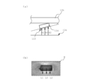
- 1A and 1B are explanatory diagrams for explaining the shape of an image of a child part in three-dimensional image data, in which (a) shows the irradiation direction of radiation emitted from a radiation generator to the child part, and (b) shows the shape of the image of the child part.
- 5A and 5B are explanatory diagrams showing cross-sectional images of a child part, in which FIG. 5A shows a cross-sectional image in a real image region, and FIG. 5B shows a cross-sectional image in a virtual image region.
- FIG. 5A shows a cross-sectional image in a real image region
- FIG. 5B shows a cross-sectional image in a virtual image region.
- FIG. 11 is an explanatory diagram for calculating tilt information of a specific surface (the surface facing the substrate surface of the sub-component) of a component attached to a substrate of an object to be inspected, in which (a) shows a tilted sub-component, and (b) shows multiple locations for calculating the width (amount of blur) for the tilt information.
- 13 is an explanatory diagram for explaining a modified example of the height information calculation process.
- the inspection device 1 is configured to have a control unit 10, which is made up of a processing device such as a personal computer (PC), a monitor 11, and an imaging unit 32.
- the imaging unit 32 also has a radiation generator 22, a substrate holding unit 24, a detector 26, a radiation quality changing unit 14, a radiation generator driving unit 16, a substrate holding unit driving unit 18, and a detector driving unit 20.
- the radiation generator 22 is a device (ray source) that generates radiation such as X-rays, and generates radiation by colliding accelerated electrons with a target such as tungsten or diamond.
- a target such as tungsten or diamond.
- the radiation in this embodiment is described as being X-rays, the radiation is not limited to this.
- the radiation may be alpha rays, beta rays, gamma rays, ultraviolet rays, visible light, or infrared rays.
- the radiation may also be microwaves or terahertz waves.
- the board holding unit 24 holds an electronic board (hereinafter simply referred to as "board") which is the object under inspection 12.
- the object under inspection 12 held by the board holding unit 24 is irradiated with radiation generated by the radiation generator 22, and the radiation which has passed through the object under inspection 12 is detected by the detector 26 to capture an image.
- the radiation transmission image of the object under inspection 12 captured by the detector 26 will be referred to as a "transmission image.”
- the board holding unit 24 which holds the board which is the object under inspection 12, and the detector 26 are moved relative to the radiation generator 22 to obtain multiple transmission images, and a reconstructed image (cross-sectional image) which is a three-dimensional image is generated from these transmission images.
- the transmission image captured by the detector 26 (transmission image data, which is data of the transmission image output from the detector 26) is sent to the control unit 10, and is reconstructed into image data including the three-dimensional shape of the solder at the joint portion using a known technique such as the Filtered Backprojection method (FBP method).
- FBP method Filtered Backprojection method
- the reconstructed image data and transmission image data are stored in a storage in the control unit 10 (for example, the storage unit 34 described later) or an external storage (not shown).
- image data obtained by extracting one cross section of the three-dimensional shape calculated based on the transmission image data is called a cross-sectional image (cross-sectional image data).
- a set of one or more cross-sectional image data is called "three-dimensional image data" or "reconstructed image data”.
- image data obtained by cutting out an arbitrary cross section from the reconstructed image data is cross-sectional image data.
- Such reconstructed images and cross-sectional images are output to the monitor 11.
- the monitor 11 In addition to the reconstructed images and cross-sectional images, the monitor 11 also displays the inspection results of the solder joint state described later.
- the reconstructed image in this embodiment is also called "planar CT” because it is reconstructed from a planar image (transmission image data) captured by the detector 26 as described above.
- the radiation quality change unit 14 changes the radiation quality generated by the radiation generator 22.
- the radiation quality is determined by the voltage (hereafter referred to as “tube voltage”) applied to accelerate the electrons to be collided with the target, and the current (hereafter referred to as "tube current") that determines the number of electrons.
- the radiation quality change unit 14 is a device that controls the tube voltage and tube current. This radiation quality change unit 14 can be realized using known technology such as a transformer or rectifier.
- the quality of radiation is determined by the brightness and hardness of the radiation (spectral distribution of radiation).
- Increasing the tube current increases the number of electrons that collide with the target, and the number of radiation photons generated.
- the brightness of the radiation increases.
- some components such as capacitors are thicker than other components, and in order to capture a transmission image of these components, it is necessary to irradiate them with radiation of high brightness.
- the brightness of the radiation is adjusted by adjusting the tube current.
- increasing the tube voltage increases the energy of the electrons that collide with the target, and the energy (spectrum) of the generated radiation increases.
- the tube voltage can be used to adjust the contrast of a transmission image.
- the radiation generator driving unit 16 has a driving mechanism such as a motor (not shown) and can move the radiation generator 22 up and down along axis A passing through its focal point (axis (optical axis) passing through the center of the radiation direction of the radiation emitted from the radiation generator 22, the direction of this axis being referred to as the "Z-axis direction").
- a driving mechanism such as a motor (not shown) and can move the radiation generator 22 up and down along axis A passing through its focal point (axis (optical axis) passing through the center of the radiation direction of the radiation emitted from the radiation generator 22, the direction of this axis being referred to as the "Z-axis direction").
- This makes it possible to change the distance between the radiation generator 22 and the inspected object (substrate) 12 held by the substrate holding unit 24 to change the irradiation field and change the magnification ratio of the transmitted image captured by the detector 26.
- the position of the radiation generator 22 in the Z-axis direction is detected by
- the detector driving unit 20 also has a driving mechanism such as a motor (not shown) and rotates the detector 26 along the detector rotation track 30.
- the substrate holding unit driving unit 18 also has a driving mechanism such as a motor (not shown) and moves the substrate holding unit 24 in parallel on the plane on which the substrate rotation track 28 is provided.
- the substrate holding unit 24 is configured to rotate on the substrate rotation track 28 in conjunction with the rotation of the detector 26. This makes it possible to capture multiple transmission images with different projection directions and projection angles while changing the relative positional relationship between the test object 12 held by the substrate holding unit 24 and the radiation generator 22.
- the area on the test object 12 where a transmission image can be acquired is determined by the size of the area where the detector 26 detects radiation and the relative positions of the radiation generator 22, the test object 12 (substrate holding unit 24), and the detector 26.
- the area where this transmission image can be acquired is called the "FOV (field of view)".
- the rotation radius of the substrate rotation orbit 28 and the detector rotation orbit 30 is not fixed, but can be freely changed. This makes it possible to arbitrarily change the irradiation angle of the radiation irradiated to the substrate, which is the inspected object 12, and the components attached to this substrate.
- the orbital plane of the substrate rotation orbit 28 and the detector rotation orbit 30 is perpendicular to the Z-axis direction described above, and if the directions perpendicular to this orbital plane are the X-axis direction and the Y-axis direction, the positions of the substrate holder 24 in the X-axis direction and the Y-axis direction are detected by the substrate position detector 29 and output to the control unit 10, and the positions of the detector 26 in the X-axis direction and the Y-axis direction are detected by the detector position detector 31 and output to the control unit 10.
- the control unit 10 controls all operations of the inspection device 1 described above. Below, the main functions of the control unit 10 are explained using FIG. 2. Although not shown, input devices such as a keyboard and a mouse are connected to the control unit 10.
- the control unit 10 includes a memory unit 34, an imaging processing unit 35, a cross-sectional image generating unit 36, a board inspection surface detecting unit 38, a pseudo cross-sectional image generating unit 40, and an inspection unit 42.
- the imaging processing unit 35 of the control unit 10 also has the function of an imaging control unit that controls the operation of the radiation quality changing unit 14, the radiation generator driving unit 16, the board holding unit driving unit 18, and the detector driving unit 20.
- each of these functional blocks is realized by the cooperation of hardware, such as a CPU that executes various arithmetic processes, and a RAM that is used as a work area for storing data and executing programs, and software. Therefore, these functional blocks can be realized in various ways by combining hardware and software.
- the memory unit 34 stores information such as imaging conditions for capturing a transmission image of the substrate, which is the inspected object 12, and the design of the substrate.
- the memory unit 34 also stores image data such as transmission images and reconstructed images (cross-sectional images, pseudo-cross-sectional images) of the substrate, as well as the inspection results of the inspection unit 42, which will be described later.
- the memory unit 34 also stores information for driving the radiation generator driving unit 16, the substrate holding unit driving unit 18, and the detector driving unit 20 (e.g., the speed at which the radiation generator driving unit 16 drives the radiation generator 22, the speed at which the substrate holding unit driving unit 18 drives the substrate holding unit 24, and the speed at which the detector driving unit 20 drives the detector 26).
- the imaging processing unit 35 drives the radiation generator 22, the substrate holding unit 24, and the detector 26 using the radiation generator driving unit 16, the substrate holding unit driving unit 18, and the detector driving unit 20 to image the specimen 12 held by the substrate holding unit 24, obtain transmission image data, and generate reconstructed image data (cross-sectional image data) from the transmission image data.
- the method of obtaining the transmission image data (capturing the transmission image) and generating the reconstructed image data (cross-sectional image data) by this imaging processing unit 35 will be described later.
- the cross-sectional image generating unit 36 generates reconstructed image data (cross-sectional image data) based on the multiple transmission image data acquired from the storage unit 34. This can be achieved using known techniques, such as the FBP method or the maximum likelihood estimation method. Different reconstruction algorithms result in different properties of the reconstructed image data and different times required for reconstruction. Therefore, multiple reconstruction algorithms and parameters used in the algorithms may be prepared in advance and the user may select one. This provides the user with the freedom to choose, such as prioritizing a shorter reconstruction time or prioritizing better image quality even if it takes more time.
- Each of the generated cross-sectional image data is stored in the storage unit 34 together with attribute information, such as information that determines the position of each cross-sectional image data in the Z-axis direction and the positions (coordinates) of pixels in the cross-sectional image data in the X-axis direction and the Y-axis direction.
- the board inspection surface detection unit 38 identifies image data (cross-sectional image data) that shows the surface to be inspected on the board, which is the inspected object 12, from among the multiple cross-sectional image data generated by the cross-sectional image generation unit 36 (for example, the top surface of the board, which will be referred to as the "board inspection surface”).
- image data cross-sectional image data
- the cross-sectional image cross-sectional image data
- the board inspection surface image data inspection surface image data
- the pseudo cross-sectional image generating unit 40 images the area of the board thicker than the cross-sectional image by stacking a predetermined number of consecutive cross-sectional images (cross-sectional image data) for the cross-sectional image data generated by the cross-sectional image generating unit 36.
- the number of cross-sectional images to be stacked is determined by the thickness of the area of the board shown by the cross-sectional image (hereinafter referred to as the "slice thickness") and the slice thickness of the pseudo cross-sectional image.
- the inspection surface image data identified by the board inspection surface detection unit 38 is used to identify the position of the solder.
- the inspection unit 42 is configured to execute various control processes for inspection using the cross-sectional image data generated by the cross-sectional image generating unit 36, the inspection surface image data identified by the board inspection surface detecting unit 38, and the pseudo cross-sectional image data generated by the pseudo cross-sectional image generating unit 40, based on the board inspection data stored in the storage unit 34.
- the board inspection data is inspection data created for each type of board.
- An inspection area (hereinafter referred to as an "inspection window”) is set for each location on the image data of the inspected object 12 where inspection is performed, and the inspection data is composed of inspection items set for each inspection window and inspection standards that serve as the criteria for determining whether the product is good or bad.
- One or more inspection windows are set for each inspection item.
- inspection windows in the same number as the number of solder application areas of the component are usually set in an arrangement corresponding to the arrangement of the solder application areas.
- the contents of the image processing are also included in the inspection data.
- the inspection unit 42 inspects the state of the solder joint. Since the solder that joins the board and the component is located near the board inspection surface, it is possible to determine whether the solder is properly joining the board and the component by inspecting the inspection surface image data and the cross-sectional image data that shows the area on the radiation generator 22 side relative to the inspection surface image data.
- solder joint condition refers to whether or not the board and the component are joined by solder and an appropriate conductive path is created. Inspection of the solder joint condition includes bridge inspection, molten state inspection, and void inspection. “Bridge” refers to an undesirable conductive path between conductors caused by solder joining. “Melted state” refers to a state in which the joint between the board and the component is insufficient due to insufficient melting of the solder, that is, whether or not there is a so-called “floating” state. "Void” refers to a defect in the solder joint caused by air bubbles in the solder joint. Therefore, the inspection unit 42 includes a bridge inspection unit 44, a molten state inspection unit 46, and a void inspection unit 48.
- bridge inspection unit 44 inspects and voids, respectively, based on the pseudo cross-sectional image data generated by the pseudo cross-sectional image generation unit 40
- the molten state inspection unit 46 inspects the molten state of the solder based on the inspection surface image data identified by the board inspection surface detection unit 38.
- the inspection results in the bridge inspection unit 44, molten state inspection unit 46, and void inspection unit 48 are stored in the memory unit 34.
- the inspection unit 42 also has a height information calculation unit 50 that calculates height information of a specific surface of a component attached to the inspected object 12 based on cross-sectional image data and pseudo cross-sectional image data including inspection surface image data. For this purpose, an inspection window is set in the board inspection data so as to include the specific surface of the component (the above-mentioned child component 12d) for which height information is to be obtained.
- the height information calculated by the height information calculation unit 50 is stored in the memory unit 34.
- FIGS. 3 to 5 are flowcharts showing the flow (inspection process) of capturing a transmission image (obtaining transmission image data), generating reconstructed image data (cross-sectional image data), identifying inspection surface image data, generating a pseudo cross-sectional image, and performing the inspection (obtaining solder joint condition and height information).
- the process in this flowchart begins, for example, when the control unit 10 receives an instruction to start the inspection from an input device (not shown).
- the imaging processing unit 35 of the control unit 10 sets the irradiation field of radiation emitted from the radiation generator 22 by the radiation generator driving unit 16 (the imaging area where the radiation is irradiated to obtain the transmission image data of the field of view FOV described above) (step S100), and starts the image acquisition and judgment process.
- the imaging areas (FOV) are selected and set in a predetermined order.
- the image capture processing unit 35 of the control unit 10 executes a transmission image capture and reconstructed image generation process, captures the test object 12 to acquire transmission image data, and generates reconstructed image data using the transmission image data (step S102). Specifically, in the transmission image capture and reconstructed image generation process S102, the image capture processing unit 35 of the control unit 10 moves the substrate holding unit 24 by the substrate holding unit drive unit 18, and moves the detector 26 by the detector drive unit 20 to change the imaging position, while setting the radiation quality of the radiation generator 22 by the radiation quality change unit 14, irradiates the current imaging field (FOV) of the test object 12 with radiation, acquires transmission image data, and stores it in the storage unit 34.
- FOV current imaging field
- the cross-sectional image generation unit 36 of the control unit 10 reads out a plurality of transmission image data from the storage unit 34, generates reconstructed image data (cross-sectional image data) using the transmission image data, and stores it in the storage unit 34.
- the movement path of the substrate holder 24 by the substrate holder driver 18 and the movement path of the detector 26 by the detector driver 20 when acquiring the transmission image data are set in advance in the substrate holder driver 18 and the detector driver 20 by reading information stored in the memory 34 or inputting information from an input device.
- the position of the radiation generator 22 in the Z-axis direction is also set in advance in the radiation generator driver 16 by a similar method.
- the substrate holder driver 18 and the detector driver 20 may move the substrate holder 24 and the detector 26 to a desired position, and the substrate holder 24 and the detector 26 may be stopped at a position where the transmission image data is acquired before acquiring the transmission image data, or the substrate holder driver 18 and the detector driver 20 may move the substrate holder 24 and the detector 26 to a desired position and acquire the transmission image data.
- the acquired transmission image data is stored in the memory 34 for each imaging area (FOV).
- the board inspection surface detection unit 38 of the control unit 10 receives the transmission image data or the reconstructed image data (cross-sectional image data) from the cross-sectional image generation unit 36, and executes a board inspection surface detection/pseudo cross-sectional image generation process to identify the inspection surface image from the received data (step S104).
- the storage unit 34 stores in advance cross-sectional image data (called "reference image data") of the board inspection surface of a normal inspected object 12 that has no abnormalities in the solder joint state, etc.
- the board inspection surface detection unit 38 of the control unit 10 compares the reference image data with each of the cross-sectional image data generated in step S102, identifies the cross-sectional image data that most closely matches the reference image data as the inspection surface image data, stores the identified cross-sectional image data (inspection surface image data) in the storage unit 34, and stores the position in the Z-axis direction in the storage unit 34 as the position of the board inspection surface in the current field of view FOV.
- the pseudo cross-sectional image generating unit 40 of the control unit 10 generates pseudo cross-sectional image data based on the identified inspection surface image data and the position of the substrate inspection surface in the Z-axis direction, and stores the data in the storage unit 34.
- multiple cross-sectional image data are generated as reconstructed image data from the transmission image data, and reference image data is determined for the cross-sectional image data, and pseudo cross-sectional image data is generated.
- the reference image data may be determined and pseudo cross-sectional image data may be generated, and the next cross-sectional image data may be generated.
- the inspection unit 42 of the control unit 10 selects one of the inspection windows set in the current field of view (FOV) (step S106) and executes the judgment process (inspection) set in the inspection window (step S108). The specific contents of the judgment process will be described later. Then, when the judgment process of the currently selected inspection window is completed, the inspection unit 42 of the control unit 10 judges whether or not there is a next inspection window (step S110). If it is determined that there is a next inspection window (step S110: Y), the process returns to step S106 to select the next inspection window and repeat the judgment process.
- FOV current field of view
- step S110: N the imaging processing unit 35 of the control unit 10 judges whether or not there is a next imaging field (FOV) (step S112). If it is determined that there is a next imaging field (step S112: Y), the process returns to step S100 to select the next imaging field (FOV) and repeat the image acquisition and judgment process. On the other hand, if the imaging processing unit 35 of the control unit 10 determines that there is no next imaging region (FOV) (step S112: N), the inspection process ends, and the control unit 10 removes the inspected object 12 from the inspection device 1.
- FOV next imaging field
- image acquisition and determination processing may be performed for each imaging field (FOV), or the examination may be performed in parallel with the acquisition of transmission image data and generation of reconstructed image data for other imaging fields (FOVs), starting from the imaging field (FOV) for which generation of reconstructed image data (cross-sectional image data and pseudo cross-sectional image data) has been completed.
- the bridge inspection unit 44 of the control unit 10 obtains a pseudo cross-sectional image of the same slice thickness as the solder ball that shows the solder ball from the pseudo cross-sectional image generation unit 40 (read from the storage unit 34), and inspects the presence or absence of a bridge in the currently selected inspection window (step S200). If no bridge is detected (step S202: N), the molten state inspection unit 46 of the control unit 10 obtains an inspection surface image from the board inspection surface detection unit 38 (read from the storage unit 34), and inspects the presence or absence of the solder in the currently selected inspection window (step S204).
- step S206: Y If the solder is melted (step S206: Y), the void inspection unit 48 of the control unit 10 obtains a pseudo cross-sectional image that partially shows the solder ball from the pseudo cross-sectional image generation unit 40 (read from the storage unit 34), and inspects the presence or absence of a void in the currently selected inspection window (step S208). If no voids are found (step S210: N), the inspection unit 42 of the control unit 10 determines that the solder joint state is normal and outputs this information to the memory unit 34 (step S212).
- step S202: Y If a bridge is detected (step S202: Y), the solder is not melted (step S206: N), or a void is present (step S210: Y), the inspection unit 42 determines that the solder joint state is abnormal and outputs this information to the memory unit 34 (step S214). When the solder state is output to the memory unit 34, the joint state determination process in this flowchart is terminated. Note that the bridge inspection, melted state inspection, and void inspection may be performed in parallel.
- the upper surface (above-mentioned board inspection surface) 12e of board 12a is set as a reference surface (reference surface) for component 12b attached to board 12a, and the distance (height information H) in the Z-axis direction between this reference surface and a surface 12f of child component 12d facing board 12a (lower surface of child component 12d in Fig. 6, the above-mentioned predetermined surface) can be measured, and it can be determined whether child component 12d is correctly mounted on component 12b or not based on this height information H.
- a method of calculating height information H from board inspection surface 12e of board 12a to surface 12f of child component 12d facing board 12a in the inspection device 1 according to this embodiment will be explained.
- the inspection object 12 (substrate holder 24) and detector 26 are moved relative to the radiation generator 22 to acquire transmission image data of the inspection object 12. Therefore, as shown in FIG. 7(a), transmission image data is acquired in which radiation is irradiated from an oblique direction onto the component 12b and the sub-component 12d.
- transmission image data is acquired in which radiation is irradiated from an oblique direction onto the component 12b and the sub-component 12d.
- the image I of the sub-component 12d in this three-dimensional image data has a shape extending in the Z-axis direction, as shown in FIG. 7(b).
- the portion of the image I that represents the image of the sub-component 12d is called the real image region Rr
- the portion formed by reconstruction is called the virtual image region Rv.
- Figure 8 shows cross-sectional images of an image I of a child part 12d in an inspection window W for inspecting the child part 12d, and each cross-sectional image shows the change in brightness value of pixels on a line L extending from the center of the child part 12d in a direction approximately perpendicular to the long side of the child part 12d.
- the cross-sectional image Ir of the real image region Rr appears clear
- the cross-sectional image Iv of the virtual image region Rv appears blurry.
- the brightness value changes suddenly at the outer shape (hereinafter referred to as "edge") of the child part 12d, and the change in brightness value is gradual in the cross-sectional image Iv in the virtual image region Rv. Therefore, in this embodiment, the amount of blurring of the edge in the image I of the child component 12d (the degree of rapidity of change in brightness value at the edge) is calculated for each cross-sectional image, and the boundary between the virtual image region Rv and real image region Rr of the child component 12d is determined based on this amount of blurring, and the boundary is determined to be the position of the surface 12f of the child component 12d that faces the board 12a.
- the amount of blur is calculated as the width D, which is the distance from the pixel of the threshold value set as the lower limit to the pixel of the threshold value set as the upper limit among the changes in brightness value at the edge of the image I (Ir, Iv) of the child part 12d.
- the width D is the distance in the direction of the arrow of the line L from the pixel whose brightness value has exceeded or reached the lower limit to the pixel just before it exceeds the upper limit or has reached the upper limit.
- the width D may be expressed in number of pixels (pixels), or may be expressed by converting the pixel pitch into a length (mm, etc.).
- the width (amount of blur) Dr in the real image region Rr is smaller than the width (amount of blur) Dv in the virtual image region Rv. Therefore, the value of the width (amount of blur) D in the cross-sectional image where the virtual image region Rv and real image region Rr switch is set as a threshold value, and the position of the cross-sectional image data when the width D changes from a width D greater than the threshold value to a width D less than the threshold value as viewed from the reference surface side is determined to be the position of the surface 12f of the child component 12d facing the board 12a.
- the width D which is the amount of blur, may be the distance (distance) between the pixel with the minimum brightness value and the pixel with the maximum brightness value among the brightness values of the pixels on the line L described above.
- the outermost pixel (farthest from the center of the child component 12d) among those pixels may be the pixel with the minimum value
- the innermost pixel (closest to the center of the child component 12d) among those pixels may be the pixel with the maximum value.
- the minimum and maximum value pixels are essentially located near the boundary, and the distance (width D) between the maximum and minimum value pixels is used as the amount of blur, making it easier to calculate the amount of blur (width D).
- width D the distance between the maximum and minimum pixels as the amount of blur
- the calculation of width D is less affected by changes in the luminance value in each cross-sectional image data, and this improves the accuracy of determining the boundary between the virtual image region Rv and the real image region Rr based on the amount of blur (width D), i.e., the position of the surface 12f of the child component 12d that faces the board 12a.
- the pseudo cross-sectional image generating unit 40 can generate pseudo cross-sectional image data by extracting about 30 pieces of cross-sectional image data with a slice thickness of 10 ⁇ m from the substrate inspection surface 12e to the radiation generator 22 side.
- the number of cross-sectional image data constituting the pseudo cross-sectional image data is determined depending on the distance from the top surface of the substrate 12a to the surface 12f of the child component 12d facing the substrate 12a and the slice thickness.
- the inspection unit 42 judges that the inspection in the currently selected inspection window is a calculation processing of height information of a predetermined surface of the component 12b attached to the inspected object 12 (the surface (lower surface) 12f of the child component 12d attached to the board 12a side of the component 12b and arranged so as to face the board inspection surface 12e)
- the inspection unit 42 of the control unit 10 executes the height information calculation processing shown in FIG. 5 for the currently selected inspection window. It is assumed that a cross-sectional image of the child component 12d is captured in the currently selected inspection window W.
- the height information calculation unit 50 of the control unit 10 identifies the position of a specific surface in the currently selected inspection window W, i.e., the position of the child part 12d (step S300).
- the inspection window W is set at the same position on the board in the multiple cross-sectional image data constituting the pseudo cross-sectional image data.
- the average value of the same pixel value in all cross-sectional image data constituting the pseudo cross-sectional image data generated in step S104 is calculated, and further, a binarization process is performed on each average value (for example, a process in which a pixel value greater than a predetermined threshold is set to the maximum value, and a pixel value equal to or less than the predetermined threshold is set to the minimum value).
- a binarization process is performed on each average value (for example, a process in which a pixel value greater than a predetermined threshold is set to the maximum value, and a pixel value equal to or less than the predetermined threshold is set to the minimum value).
- the height information calculation unit 50 of the control unit 10 determines the center of the child part 12d (the center of gravity of the pixel set to the minimum value) based on the position of the child part 12d identified in step S300 (the pixel (black pixel) set to the minimum value in the current inspection window W is the image of the child part 12d) (step S302).
- the height information calculation unit 50 of the control unit 10 selects one piece of cross-sectional image data from the pseudo cross-sectional image data (step S304).
- cross-sectional image data is selected from the reference image data side (the side of the board inspection surface 12e, which is the reference surface) toward the radiation generator 22 side.
- the height information calculation unit 50 of the control unit 10 calculates the above-mentioned width (amount of blur) D (step S306) using pixel values (brightness values) of a predetermined range on a line L that intersects (approximately perpendicular to) an edge (e.g., an edge on the long side) of the child part 12d determined in step S302 from the center of the child part 12d toward the outer periphery of the inspection window W, within the currently selected inspection window in the selected cross-sectional image data.
- the height information calculation unit 50 of the control unit 10 selects the next cross-sectional image data (step S308).
- the height information calculation unit 50 of the control unit 10 calculates the width (amount of blur) D of the currently selected examination window W at the same position (line L intersecting with the edge) as the previous cross-sectional image in the selected cross-sectional image data (next cross-sectional image data) (step S310).
- the height information calculation unit 50 of the control unit 10 determines whether the amount of blur D satisfies a predetermined judgment condition (step S312).
- the amount of blur of the currently selected cross-sectional image data (the amount of blur calculated in step S310) is compared with the amount of blur of the cross-sectional image data (previous cross-sectional image data) adjacent to the reference surface side (the side of the board inspection surface 12e) of this cross-sectional image data (the amount of blur calculated in step S306), and when the amount of blur of the previous cross-sectional image data is greater than a predetermined threshold and the amount of blur of the currently selected cross-sectional image data has changed to a value equal to or less than the predetermined threshold, it is determined that the predetermined judgment condition is satisfied.
- step S312 determines that the amount of blur does not satisfy the predetermined judgment condition (step S312: N), it returns to step S308, selects the next cross-sectional image data, and repeats the subsequent processes.
- step S312: Y determines the position (position in the Z axis direction) of the currently selected cross-sectional image data as the position of the surface 12f (a predetermined surface of the component 12b) of the child component 12d facing the board 12a (step S314), calculates the height information H of the predetermined surface 12f in the currently selected inspection window from the position in the Z axis direction of the reference image data (cross-sectional image data of the board inspection surface) which is the reference surface (step S316), and ends the height information calculation process.
- the cross-sectional image data constituting the pseudo cross-sectional image data is selected in order from the reference surface side (the side of the board inspection surface 12e) to calculate the amount of blur, and the amount of blur of the currently selected cross-sectional image data is compared with the amount of blur of the previous cross-sectional image data (the cross-sectional image data adjacent to the board inspection surface 12e side of the currently selected cross-sectional image data) to determine the position in the Z-axis direction of a specific surface (surface facing the board surface side of the child component 12d) 12f of the component 12b.
- the above-mentioned blur amount determination process may be performed in order from the cross-sectional image data constituting the pseudo cross-sectional image data that are offset by a specific amount from the reference surface (reference image data), or a binary search may be performed based on the position of the reference surface (reference image data) and the offset position to perform the above-mentioned blur amount determination process.
- the board inspection surface 12e is used as the reference surface for calculating the height information, but the reference surface may be set at another position (for example, the back surface of the board 12a or a specified surface of the board holding portion 24 that holds the board 12a).
- the height information of a predetermined surface 12f of the component 12b (the surface of the child component 12d facing the board 12a) can be calculated using the pseudo cross-sectional image data used in the solder joint state determination processing.
- the height information can be calculated without depending on the manufacturing variation of the child component 12d (e.g., a chip, etc.).
- the edge width (blur amount) is calculated from the luminance value of the pixel on the line L0 extending from the center of the child component 12d in a direction substantially perpendicular to the long side of the child component 12d to determine the height information H0, and the edge width (blur amount) on a line different from the line L0 is calculated to determine the height information, thereby calculating the inclination information of the surface 12f of the child component 12d facing the board surface.
- the width (amount of blur) of the edges of two lines L1 and L2 located in the long side direction on either side of the center of child component 12d is calculated to determine the respective height information H1 and H2, and the inclination information of child component 12d (inclination information of surface 12f facing the board surface of child component 12d) is calculated using this height information H0, H1, and H2.
- the height information calculation unit 50 of the control unit 10 calculates the widths (amounts of blur) of multiple locations (for example, three locations of lines L0, L1, and L2 in the case of FIG. 9) within the examination window of the currently selected cross-sectional image data in step S306 in the height information calculation process shown in FIG. 5.
- the height information calculation unit 50 of the control unit 10 also calculates the widths (amounts of blur) of multiple locations within the examination window of the currently selected cross-sectional image data in step S310.
- step S312 the height information calculation unit 50 of the control unit 10 determines whether the amount of blur at each location satisfies the judgment condition, and for the locations that satisfy the judgment condition, stores the location in association with the position of the cross-sectional image data when the judgment condition was satisfied, and returns to step S308 to repeat the subsequent processes until all locations satisfy the judgment condition. Then, when the height information calculation unit 50 of the control unit 10 determines that the judgment conditions are satisfied at all locations, in step S316, it calculates height information for each location from the position of the cross-sectional image data that satisfies the judgment conditions for each location (for example, height information H0, H1, and H2 in the case of FIG. 9), and calculates tilt information for child component 12d (tilt information for surface 12f of child component 12d that faces the board surface) from this height information.
- height information for child component 12d tilt information for surface 12f of child component 12d that faces the board surface
- the height information calculation unit 50 of the control unit 10 selects the cross-sectional image data extracted as the pseudo cross-sectional image data from the side farthest from the reference surface (reference image data), and executes the above-mentioned judgment process, thereby determining the position of the upper surface 12f' of the child component 12d' from the position in the Z-axis direction of the cross-sectional image data when the judgment condition is satisfied (comparing the amount of blur of the currently selected cross-sectional image data (the amount of blur calculated in step S310) with the amount of blur of the cross-sectional image data adjacent to the opposite side of the board inspection surface 12e of this cross-sectional image data (the amount of blur calculated in step S306), and determining the position of the upper surface 12f' of the child component 12d' and calculating its height information H'.
- the pseudo cross-sectional image data needs to be composed of cross-sectional image data of a wider range than when calculating height information of the surface of the component 12b on the board 12a side. Also, by calculating height information of a plurality of locations by the above-mentioned method, the inclination information of the surface of the component 12b opposite to the board 12a (surface 12f' opposite to the board 12a of the child component 12d' attached to the surface of the component 12b opposite to the board 12a) can be calculated using the height information.
Landscapes
- Physics & Mathematics (AREA)
- Health & Medical Sciences (AREA)
- General Physics & Mathematics (AREA)
- Radiology & Medical Imaging (AREA)
- Biochemistry (AREA)
- Theoretical Computer Science (AREA)
- Nuclear Medicine, Radiotherapy & Molecular Imaging (AREA)
- Life Sciences & Earth Sciences (AREA)
- Chemical & Material Sciences (AREA)
- Analytical Chemistry (AREA)
- Pulmonology (AREA)
- General Health & Medical Sciences (AREA)
- Engineering & Computer Science (AREA)
- Immunology (AREA)
- Pathology (AREA)
- Electromagnetism (AREA)
- Image Processing (AREA)
Priority Applications (1)
| Application Number | Priority Date | Filing Date | Title |
|---|---|---|---|
| JP2025513885A JPWO2024214554A1 (https=) | 2023-04-12 | 2024-03-28 |
Applications Claiming Priority (2)
| Application Number | Priority Date | Filing Date | Title |
|---|---|---|---|
| JP2023-065250 | 2023-04-12 | ||
| JP2023065250 | 2023-04-12 |
Publications (1)
| Publication Number | Publication Date |
|---|---|
| WO2024214554A1 true WO2024214554A1 (ja) | 2024-10-17 |
Family
ID=93059327
Family Applications (1)
| Application Number | Title | Priority Date | Filing Date |
|---|---|---|---|
| PCT/JP2024/012697 Ceased WO2024214554A1 (ja) | 2023-04-12 | 2024-03-28 | 検査装置 |
Country Status (2)
| Country | Link |
|---|---|
| JP (1) | JPWO2024214554A1 (https=) |
| WO (1) | WO2024214554A1 (https=) |
Citations (4)
| Publication number | Priority date | Publication date | Assignee | Title |
|---|---|---|---|---|
| JPH07221151A (ja) * | 1994-01-19 | 1995-08-18 | Internatl Business Mach Corp <Ibm> | 部品間の接合部を検査する方法および装置 |
| JP2003514233A (ja) * | 1999-11-08 | 2003-04-15 | ニコレット イメージング システムズ | 垂直スライスイメージングを利用した検査方法 |
| JP2010145359A (ja) * | 2008-12-22 | 2010-07-01 | Omron Corp | X線検査装置、x線検査方法およびx線検査プログラム |
| JP2021173575A (ja) * | 2020-04-22 | 2021-11-01 | 株式会社サキコーポレーション | 検査装置 |
-
2024
- 2024-03-28 WO PCT/JP2024/012697 patent/WO2024214554A1/ja not_active Ceased
- 2024-03-28 JP JP2025513885A patent/JPWO2024214554A1/ja active Pending
Patent Citations (4)
| Publication number | Priority date | Publication date | Assignee | Title |
|---|---|---|---|---|
| JPH07221151A (ja) * | 1994-01-19 | 1995-08-18 | Internatl Business Mach Corp <Ibm> | 部品間の接合部を検査する方法および装置 |
| JP2003514233A (ja) * | 1999-11-08 | 2003-04-15 | ニコレット イメージング システムズ | 垂直スライスイメージングを利用した検査方法 |
| JP2010145359A (ja) * | 2008-12-22 | 2010-07-01 | Omron Corp | X線検査装置、x線検査方法およびx線検査プログラム |
| JP2021173575A (ja) * | 2020-04-22 | 2021-11-01 | 株式会社サキコーポレーション | 検査装置 |
Also Published As
| Publication number | Publication date |
|---|---|
| JPWO2024214554A1 (https=) | 2024-10-17 |
Similar Documents
| Publication | Publication Date | Title |
|---|---|---|
| JP5559551B2 (ja) | 検査装置 | |
| US8351682B2 (en) | X-ray examination region setting method, X-ray examination apparatus and X-ray examination region setting program | |
| JP5646769B2 (ja) | X線検査方法及び装置 | |
| US10054432B2 (en) | X-ray inspection apparatus and control method | |
| US11835475B2 (en) | Inspection position identification method, three-dimensional image generation method, and inspection device | |
| US20110222655A1 (en) | X-ray inspection apparatus, x-ray inspection method, x-ray inspection program, and x-ray inspection system | |
| US11475556B2 (en) | Method and apparatus for rapidly classifying defects in subcomponents of manufactured component | |
| JPH02138855A (ja) | X線透過画像によるはんだ付部の検査方法及びその装置 | |
| US12228527B2 (en) | Inspection device | |
| JP7542327B2 (ja) | 検査装置 | |
| JP4228773B2 (ja) | 基板検査装置 | |
| WO2024214554A1 (ja) | 検査装置 | |
| JP6676023B2 (ja) | 検査位置の特定方法及び検査装置 | |
| US11521309B2 (en) | Method and apparatus for rapid inspection of subcomponents of manufactured component | |
| JP5432795B2 (ja) | 検査装置 | |
| JP4449596B2 (ja) | 実装基板検査装置 | |
| WO2024210035A1 (ja) | 画像データの補正方法及び検査装置 | |
| JPH05251535A (ja) | バンプ検査装置 | |
| TWI920742B (zh) | 檢查系統、檢查裝置、檢查方法及程式 | |
| TW202518009A (zh) | 檢查系統、檢查裝置、檢查方法及程式 | |
| WO2024117099A1 (ja) | 検査装置 | |
| JP2021183938A (ja) | X線検査装置、x線検査方法およびx線検査プログラム | |
| KR100300586B1 (ko) | X-ray를이용한인쇄회로기판의단층검사장치및검사방법 | |
| JP2026040849A (ja) | 画像データの生成方法及び検査装置 | |
| JP2025139723A (ja) | 不良検知装置及び不良検知方法 |
Legal Events
| Date | Code | Title | Description |
|---|---|---|---|
| 121 | Ep: the epo has been informed by wipo that ep was designated in this application |
Ref document number: 24788582 Country of ref document: EP Kind code of ref document: A1 |
|
| ENP | Entry into the national phase |
Ref document number: 2025513885 Country of ref document: JP Kind code of ref document: A |
|
| WWE | Wipo information: entry into national phase |
Ref document number: 2025513885 Country of ref document: JP |
|
| NENP | Non-entry into the national phase |
Ref country code: DE |
|
| 122 | Ep: pct application non-entry in european phase |
Ref document number: 24788582 Country of ref document: EP Kind code of ref document: A1 |