WO2024214369A1 - 電磁波反射パネル、電磁波反射装置、及び電磁波反射フェンス - Google Patents
電磁波反射パネル、電磁波反射装置、及び電磁波反射フェンス Download PDFInfo
- Publication number
- WO2024214369A1 WO2024214369A1 PCT/JP2024/004181 JP2024004181W WO2024214369A1 WO 2024214369 A1 WO2024214369 A1 WO 2024214369A1 JP 2024004181 W JP2024004181 W JP 2024004181W WO 2024214369 A1 WO2024214369 A1 WO 2024214369A1
- Authority
- WO
- WIPO (PCT)
- Prior art keywords
- electromagnetic wave
- dielectric substrate
- thickness
- wave reflecting
- panel
- Prior art date
- Legal status (The legal status is an assumption and is not a legal conclusion. Google has not performed a legal analysis and makes no representation as to the accuracy of the status listed.)
- Ceased
Links
Images



Classifications
-
- H—ELECTRICITY
- H01—ELECTRIC ELEMENTS
- H01Q—ANTENNAS, i.e. RADIO AERIALS
- H01Q1/00—Details of, or arrangements associated with, antennas
- H01Q1/12—Supports; Mounting means
-
- H—ELECTRICITY
- H01—ELECTRIC ELEMENTS
- H01Q—ANTENNAS, i.e. RADIO AERIALS
- H01Q15/00—Devices for reflection, refraction, diffraction or polarisation of waves radiated from an antenna, e.g. quasi-optical devices
- H01Q15/14—Reflecting surfaces; Equivalent structures
Definitions
- the present invention relates to an electromagnetic wave reflecting panel, an electromagnetic wave reflecting device, and an electromagnetic wave reflecting fence.
- the fifth generation mobile communication system (hereinafter referred to as "5G"), which is high-speed, large-capacity, low-latency, and allows multiple simultaneous connections, provides a frequency band of 6 GHz or less called “sub-6" and a 28 GHz band classified as a millimeter wave band.
- the next generation 6G mobile communication standard is expected to expand to the terahertz band.
- the electromagnetic wave reflection panel By making the electromagnetic wave reflection panel structurally or mechanically stable, it is possible to make it resistant to use both indoors and outdoors.
- electromagnetic wave reflection panels on highways and other outdoor environments, it is important to satisfy the load strength standard for deflection due to wind pressure, etc., and the flame resistance, and it is necessary to have a certain thickness.
- chemically strengthened glass with a thickness of 8.0 mm to 17.0 mm and flame-retardant transparent plastic plates such as polycarbonate are used as windbreak fences or soundproofing walls.
- two or more dielectric substrates are usually required.
- Electromagnetic waves incident on an electromagnetic wave reflection panel lose energy due to the functional layer, i.e., transparent resins present on the incident side of the reflection layer.
- the reflection characteristics may be reduced due to the influence of the thickness of the dielectric layer such as transparent resin and the influence of the dielectric properties of the material used.
- One of the objectives of the present invention is to provide an electromagnetic wave reflective panel that suppresses the deterioration of reflective characteristics even when the overall thickness of the panel increases.
- the electromagnetic wave reflection panel has a functional layer that reflects electromagnetic waves in a predetermined frequency band ranging from 1 GHz to 300 GHz, and the deterioration of the reflection characteristics is suppressed by adjusting the thickness of a dielectric substrate such as a transparent resin that is present on the incident side of this functional layer.
- the electromagnetic wave reflection panel has a first dielectric substrate provided on the incident side of the functional layer and a second dielectric substrate provided on the functional layer opposite the first dielectric substrate, the thickness of the electromagnetic wave reflection panel is 5.0 mm to 20.0 mm, and the thickness of the first dielectric substrate is equal to or smaller than the thickness of the second dielectric substrate.
- 1 is a schematic diagram of an electromagnetic wave reflecting panel according to an embodiment
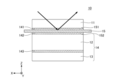
- 1 is a diagram showing an example of a layer structure of an electromagnetic wave reflection panel according to an embodiment
- 1 is a schematic diagram of an electromagnetic wave reflecting device using an electromagnetic wave reflecting panel.
- 1 is a schematic diagram of an electromagnetic wave reflecting fence formed by connecting multiple electromagnetic wave reflecting devices.
- 11A and 11B are diagrams showing the reflection mode of an electromagnetic wave reflecting panel of a comparative example.
- electromagnetic wave reflection panels are required to have a certain thickness or more from the standpoint of mechanical strength and stability.
- good reflection characteristics are maintained by appropriately selecting the thickness of the dielectric substrate on the electromagnetic wave incident side while ensuring the overall thickness of the electromagnetic wave reflection panel.
- FIG. 1 is a schematic diagram of an electromagnetic wave reflecting panel 10.
- the horizontal or width of the electromagnetic wave reflecting panel 10 is the X direction
- the vertical or height is the Y direction
- the thickness is the Z direction.
- the electromagnetic wave incident on the electromagnetic wave reflecting panel 10 is represented diagrammatically as EMWin
- the electromagnetic wave reflected from the electromagnetic wave reflecting panel 10 is represented as EMWref.
- the electromagnetic wave reflecting panel 10 has a certain overall thickness while suppressing deterioration of reflection characteristics.
- the electromagnetic wave reflecting panel 10 has a functional layer 15 that reflects electromagnetic waves in a predetermined frequency band, and a first dielectric substrate 11 and a second dielectric substrate 14 that sandwich the functional layer 15.
- the first dielectric substrate 11 is provided on the front or back surface of the functional layer 15 on which the electromagnetic waves are incident.
- the first dielectric substrate 11 is transparent to the incident electromagnetic waves EMWin and the reflected electromagnetic waves EMWref, and is also transparent to visible light if necessary.
- the second dielectric substrate 14 is provided on the side opposite to the side on which the electromagnetic waves are incident.
- the thickness t of the electromagnetic wave reflecting panel 10 is a thickness that can be used stably both indoors and outdoors, and is, for example, 5.0 mm or more and 20.0 mm or less.
- the thickness of the first dielectric substrate 11 is the same as or thinner than the thickness of the second dielectric substrate 14.
- the thicknesses of the first dielectric substrate 11 and the second dielectric substrate 14 here refer to the design thicknesses, and include cases where there are parts where the thicknesses of the first dielectric substrate 11 and the second dielectric substrate are locally reversed due to manufacturing errors, etc.
- the thickness of the first dielectric substrate 11 is less than 1/2 the thickness t of the electromagnetic wave reflecting panel 10.
- the second dielectric substrate 14 may be made thicker than the first dielectric substrate 11 to provide the electromagnetic wave reflecting panel 10 with mechanical strength and stability.
- the second dielectric substrate 14 does not need to be a single substrate, but may be two or more dielectric substrates or sheets bonded together.
- the functional layer 15 can reflect incident electromagnetic waves EMWin of a predetermined frequency band on both sides, but in order to suppress deterioration of the reflection characteristics while maintaining the overall thickness of the electromagnetic wave reflecting panel 10, the side covered by the first dielectric substrate 11 may be used as the main reflection surface.
- a mark indicating whether this is the incident side or back side of the electromagnetic waves EMW may be provided on the surface of the first dielectric substrate 11 or the surface of the opposite second dielectric substrate 14. This allows the side that is less affected by the dielectric to be correctly used as the main reflection surface when placing the electromagnetic wave reflecting panel 10 in an actual installation location.
- FIG. 2 shows an example of the layer structure of the electromagnetic wave reflecting panel 10 of the embodiment.
- the layer structure in FIG. 2 is a cross-sectional configuration in the XZ plane.
- the first dielectric substrate 11 is adhered to the first surface 151 of the functional layer 15 by an adhesive layer 141.
- the second dielectric substrate 14 is adhered to the second surface 152 of the functional layer 15 by an adhesive layer 142.
- the second dielectric substrate 14 is formed by bonding two dielectric substrates 12 and 13 with an adhesive layer 143. If a single substrate is thick enough, a single dielectric substrate may be used as the second dielectric substrate 14, or if the thickness is insufficient, the second dielectric substrate 14 may be formed from three or more dielectric substrates.
- the first dielectric substrate 11 only needs to be thick enough to protect the functional layer 15 in order to reduce the influence of the thickness and dielectric characteristics of the dielectric on the electromagnetic wave incident side as much as possible.
- the thickness of the first dielectric substrate 11 is preferably less than 1/2 the thickness of the electromagnetic wave reflection panel 10, and may be 1/3 or less of the thickness of the electromagnetic wave reflection panel 10 depending on the usage environment. If the total thickness of the functional layer 15 and the adhesive layers 141 and 142 is about 1.0 mm and the overall thickness of the electromagnetic wave reflection panel 10 is 17.0 mm, the thickness of the electromagnetic wave reflection panel 10 can be secured to ensure mechanical strength and maintain the reflection characteristics by using two dielectric substrates with a thickness of 8.0 mm.
- the reflection characteristics may be reduced on the electromagnetic wave incident side.
- the thickness of the first dielectric substrate 11 on the incident side is made smaller than the thickness of the second dielectric substrate 14.
- the combination of thicknesses of the first dielectric substrate 11 and the second dielectric substrate 14 is not limited to 8.0 mm and 8.0 mm, but may be 2.0 mm and 14.0 mm, 4.0 mm and 12.0 mm, or 6.0 mm and 10.0 mm.
- the second dielectric substrate 14 may be composed of two or more dielectric substrates or sheets.
- the first dielectric substrate 11 and the second dielectric substrate 14 may be formed of an organic material such as resin, an inorganic material, or an organic-inorganic hybrid material.
- an organic material a transparent dielectric resin sheet or plate such as polycarbonate, cycloolefin polymer (COP), polyethylene terephthalate (PET), or fluororesin may be used. These materials are also flame-retardant materials.
- Inorganic materials such as glass, silicon oxide, and quartz may be used.
- the adhesive layers 141, 142, and 143 are dielectric adhesive layers, and ethylene vinyl acetate (EVA), COP, ultraviolet curing resin, thermosetting resin, thermoplastic resin, etc. can be used.
- EVA ethylene vinyl acetate
- COP ethylene vinyl acetate
- ultraviolet curing resin urethane resin, acrylic resin, silicone resin, epoxy resin, urethane acrylate, etc.
- the materials of the adhesive layers 141, 142, and 143 may be the same or different. At least the material of the adhesive layer 141 has a relative dielectric constant and a dielectric loss tangent set in an appropriate range that suppresses a decrease in reflection efficiency.
- the relative dielectric constant of the adhesive layer 141 is 2.0 or more and less than 3.0, and the dielectric loss tangent is 0.0001 or more and less than 0.1000. If the relative dielectric constant of the adhesive layer 141 is 3.0 or more, there is a risk that the loss at high frequencies will increase. If the dielectric loss tangent of the adhesive layer 141 is 0.1000 or more, there is a risk that the loss of electrical energy in the resin film will increase.
- the functional layer 15 may have a mirror-like reflecting surface with an angle of incidence equal to the angle of reflection, or may have an artificial metasurface that reflects or diffuses the incident electromagnetic wave in a controlled direction.
- the metasurface is formed with a periodic pattern, mesh pattern, geometric pattern, etc. designed according to the desired reflection mode and frequency band, and the reflection characteristics such as the reflection angle and reflection efficiency are controlled.
- the end of the functional layer 15 does not necessarily need to protrude from the end of the laminate of the electromagnetic wave reflection panel 10, and may be folded in the thickness direction of the electromagnetic wave reflection panel 10 or cut off after the final processing step.
- FIG. 3 is a schematic diagram of an electromagnetic wave reflecting device 60 using the electromagnetic wave reflecting panel 10 of FIG. 1.
- the width or horizontal direction of the electromagnetic wave reflecting panel 10 when the electromagnetic wave reflecting device 60 is installed is the X direction
- the height or vertical direction is the Y direction
- the thickness direction is the Z direction.
- the electromagnetic wave reflecting device 60 has the electromagnetic wave reflecting panel 10 and a frame 50 that holds the electromagnetic wave reflecting panel 10.
- the frame 50 holds two sides along the height direction when the electromagnetic wave reflecting panel 10 is installed.
- a top frame 57 that holds the upper end of the electromagnetic wave reflecting panel 10 and a bottom frame 58 that holds the lower end may be provided.
- the frame 50, the top frame 57, and the bottom frame 58 form a frame that holds the entire periphery of the electromagnetic wave reflecting panel 10.
- the frame 50 may be called a "side frame” based on its positional relationship with the top frame 57 and the bottom frame 58.
- an identification mark indicating the surface on the electromagnetic wave incident side may be formed on the end of the electromagnetic wave reflecting panel 10 by laser processing or the like.
- the electromagnetic wave reflection device 60 may have legs 56 that support the frame 50. As shown in FIG. 3, it is desirable to provide legs 56 when the electromagnetic wave reflection device 60 is to be freestanding on an installation surface, but legs 56 are not essential. Casters may be provided on the legs 56 to make it mobile, or the electromagnetic wave reflection device 60 may be suspended from a ceiling or support without providing legs 56.
- FIG. 4 is a schematic diagram of an electromagnetic wave reflecting fence 100 in which electromagnetic wave reflecting devices 60-1, 60-2, and 60-3 are connected.
- three electromagnetic wave reflecting devices 60-1, 60-2, and 60-3 (hereinafter, collectively referred to as “electromagnetic wave reflecting devices 60" as appropriate) are connected to form the electromagnetic wave reflecting fence 100, but there is no particular limit to the number of electromagnetic wave reflecting devices 60 that are connected.
- the electromagnetic wave reflecting devices 60-1, 60-2, and 60-3 each have an electromagnetic wave reflecting panel 10-1, 10-2, and 10-3.
- an electromagnetic wave reflecting fence 100 is obtained that is connected in the X direction. It is desirable that the orientation of the first dielectric substrate 11 is the same at at least one point where the electromagnetic wave reflecting panels 10-1, 10-2, and 10-3 are connected. From the viewpoint of making the overall reflection characteristics of the electromagnetic wave reflecting fence 100 uniform, the thickness of the first dielectric substrate 11 used in the electromagnetic wave reflecting panels 10-1, 10-2, and 10-3 may be made approximately the same.
- An identification mark indicating the electromagnetic wave incident surface side may be formed at each end of the electromagnetic wave reflecting panels 10-1, 10-2, and 10-3, and the first dielectric substrate 11 may be aligned to the incident surface side.
- ⁇ Measurement of electromagnetic wave reflection panel characteristics In the following, multiple samples of the electromagnetic wave reflecting panel 10 are fabricated, and the reflection characteristics for the incident electromagnetic wave are measured to identify an appropriate thickness range for the first dielectric substrate 11. Throughout the examples and comparative examples, a stainless steel mesh having a thickness of 100 ⁇ m is used as the functional layer 15, and EVA is used as the adhesive layers 141 and 142. The thickness of the EVA after lamination is 400 ⁇ m each. The return loss is measured for each of the fabricated samples.
- the return loss is measured using a spectrum network analyzer and a high frequency oblique incidence free space type S parameter measurement jig. Electromagnetic waves of 28.2 GHz are vertically incident and the vertical reflection is measured. As a reference value for return loss, electromagnetic waves of 4.8 GHz and 28.0 GHz are vertically incident using a smooth aluminum plate of 3.0 mm thickness and 300.0 mm x 300.0 mm to measure the vertical reflection, and this measurement value is set as the return loss at frequencies of 4.8 GHz and 28.0 GHz of 0.00 dB. From the viewpoint of maintaining the reflection characteristics, it is desirable for the return loss (absolute value) to be 0.50 dB or less from the reference value.
- Example 2 is Example 2.
- a polycarbonate sheet having a thickness of 2.0 mm is used as the first dielectric substrate 11.
- the second dielectric substrate 14 is formed by bonding three polycarbonate sheets having a thickness of 5.0 mm.
- the three polycarbonate sheets are bonded with EVA having a thickness of 400 ⁇ m.
- the total thickness of the laminate sandwiching the functional layer 15 is 18.7 mm, and the thickness of the first dielectric substrate 11 is 1/9 or less of the thickness of the laminate.
- An electromagnetic wave of 28.2 GHz is vertically incident from the first dielectric substrate 11 side, and the return loss at an incident angle of 0° and a reflection angle of 0° at 28.2 GHz is measured by the free space method. The measurement result was ⁇ 0.21 dB. It can be seen that the thickness of the second dielectric substrate 14 does not significantly affect the return loss of the electromagnetic wave incident on the first dielectric substrate 11 side.
- Example 3 is Example 3.
- a polycarbonate sheet having a thickness of 5.0 mm is used as the first dielectric substrate 11.
- the second dielectric substrate 14 is formed by bonding two polycarbonate sheets having a thickness of 5.0 mm with EVA having a thickness of 400 ⁇ m.
- the total thickness of the laminate in which the functional layer 15 is sandwiched between the first dielectric substrate 11 and the second dielectric substrate 14 is 16.3 mm, and the thickness of the first dielectric substrate 11 is 1/3 or less of the thickness of the laminate.
- An electromagnetic wave of 28.2 GHz is vertically incident from the first dielectric substrate 11 side, and the return loss at an incidence angle of 0° and a reflection angle of 0° at 28.2 GHz is measured by the free space method. The measurement result was ⁇ 0.50 dB.
- the return loss increases as the thickness of the first dielectric substrate 11 increases, but is within the allowable range.
- Example 4 is Example 4.
- a polycarbonate sheet having a thickness of 3.0 mm is used as the first dielectric substrate 11.
- a polycarbonate sheet having a thickness of 7.0 mm is used as the second dielectric substrate 14.
- the total thickness of the laminate in which the functional layer 15 is sandwiched between two polycarbonate sheets is 10.9 mm, and the thickness of the first dielectric substrate 11 is about 1/4 of the thickness of the laminate.
- An electromagnetic wave of 28.2 GHz is vertically incident from the first dielectric substrate 11 side, and the return loss at an incidence angle of 0° and a reflection angle of 0° at 28.2 GHz is measured by the free space method. The measurement result was -0.25 dB.
- Example 5 is Example 5.
- a polycarbonate sheet having a thickness of 3.0 mm is used as the first dielectric substrate 11.
- a polycarbonate sheet having a thickness of 10.0 mm is used as the second dielectric substrate 14.
- the total thickness of the laminate in which the functional layer 15 is sandwiched between two polycarbonate sheets is 13.9 mm, and the thickness of the first dielectric substrate 11 is 1/4 or less of the thickness of the laminate.
- An electromagnetic wave of 28.2 GHz is vertically incident from the first dielectric substrate 11 side, and the return loss at an incidence angle of 0° and a reflection angle of 0° at 28.2 GHz is measured by the free space method.
- the measurement result was -0.25 dB.
- Example 6 is Example 6.
- a polycarbonate sheet having a thickness of 4.0 mm is used as the first dielectric substrate 11.
- a polycarbonate sheet having a thickness of 7.5 mm is used as the second dielectric substrate 14.
- the total thickness of the laminate in which the functional layer 15 is sandwiched between two polycarbonate sheets is 12.4 mm, and the thickness of the first dielectric substrate 11 is 1/3 or less of the thickness of the laminate.
- An electromagnetic wave of 28.2 GHz is vertically incident from the first dielectric substrate 11 side, and the return loss at an incidence angle of 0° and a reflection angle of 0° at 28.2 GHz is measured by the free space method. The measurement result was -0.42 dB.
- Example 8 is Example 8.
- a polycarbonate sheet having a thickness of 5.0 mm is used as the first dielectric substrate 11.
- a polycarbonate sheet having a thickness of 5.0 mm is used as the second dielectric substrate 14.
- the total thickness of the laminate in which the functional layer 15 is sandwiched between the first dielectric substrate 11 and the second dielectric substrate 14 is 10.9 mm, and the thickness of the first dielectric substrate 11 is less than 1/2 of the thickness of the laminate.
- An electromagnetic wave of 28.2 GHz is vertically incident from the first dielectric substrate 11 side, and the return loss at an incident angle of 0° and a reflection angle of 0° at 28.2 GHz is measured by the free space method. The measurement result was -0.50 dB.
- Example 3 This result is the same as the result of Example 3. From Examples 1 and 2, the result was derived that the thickness of the second dielectric substrate 14 on the opposite side to the incident side of the electromagnetic wave does not affect the return loss very much, but from Examples 3 and 8, the same result is derived that the thickness of the second dielectric substrate 14 does not affect the return loss very much.
- Example 9 is Comparative Example 1.
- a polycarbonate sheet having a thickness of 10.0 mm is used as the first dielectric substrate 11.
- a polycarbonate sheet having a thickness of 8.0 mm is used as the second dielectric substrate 14.
- the total thickness of the laminate in which the functional layer 15 is sandwiched between the first dielectric substrate 11 and the second dielectric substrate 14 is 16.9 mm, and the thickness of the first dielectric substrate 11 is about 5/9 of the thickness of the laminate.
- An electromagnetic wave of 28.2 GHz is vertically incident from the first dielectric substrate 11 side, and the return loss at an incidence angle of 0° and a reflection angle of 0° at 28.2 GHz is measured by the free space method. The measurement result was -0.94 dB.
- Example 9 is Comparative Example 2.
- a polycarbonate sheet having a thickness of 8.0 mm is used as the first dielectric substrate 11.
- a polycarbonate sheet having a thickness of 2.0 mm is used as the second dielectric substrate 14.
- the configuration of Example 9 is the same as that of Example 1, except that the electromagnetic wave incidence side is reversed.
- the total thickness of the laminate in which the functional layer 15 is sandwiched between the first dielectric substrate 11 and the second dielectric substrate 14 is 10.9 mm, and the thickness of the first dielectric substrate 11 accounts for more than 2/3 of the thickness of the laminate.
- An electromagnetic wave of 28.2 GHz is vertically incident from the first dielectric substrate 11 side, and the return loss at an incidence angle of 0° and a reflection angle of 0° at 28.2 GHz is measured by the free space method.
- the measurement result was -0.80B.
- Example 10 is Comparative Example 3. As shown in FIG. 5, the first dielectric substrate 11 is made of polycarbonate sheets having a thickness of 2.0 mm and a thickness of 6.0 mm, which are bonded together with EVA having a thickness of 400 ⁇ m.
- the second dielectric substrate 14 is made of a polycarbonate sheet having a thickness of 2.0 mm.
- a functional layer 15 is sandwiched between the first dielectric substrate 11 and the second dielectric substrate.
- the configuration of Example 10 is the opposite of the configuration of Example 7 in that the electromagnetic wave incidence side is oriented in the opposite direction.
- the total thickness of the laminate including EVA is 11.3 mm, and the thickness of the first dielectric substrate 11 is 2/3 or more of the thickness of the laminate.
- An electromagnetic wave of 28.2 GHz is vertically incident from the first dielectric substrate 11 side, and the return loss at an incidence angle of 0° and a reflection angle of 0° at 28.2 GHz is measured by the free space method.
- the measurement result was -1.02B.
- Examples 1 to 11 From the measurement results of Examples 1 to 11, the following can be derived.
- a) In an electromagnetic wave reflecting panel when a first dielectric substrate 11 and a second dielectric substrate 14 are provided on both sides of a functional layer 15, it is desirable to make the thickness of the first dielectric substrate 11 on the electromagnetic wave incident side equal to or thinner than the thickness of the second dielectric substrate 14.
- the second dielectric substrate 14 may be formed of two or more dielectric substrates.
- the thickness of the first dielectric substrate is desirably less than half the thickness of the entire electromagnetic wave reflecting panel.
- the deterioration of the reflection characteristics is suppressed by making the thickness of the first dielectric substrate 11 7.0 mm or less.
- the deterioration of the reflection characteristics can be suppressed more efficiently by making the thickness of the first dielectric substrate 11 less than half the thickness of the electromagnetic wave reflecting panel.
- the second dielectric substrate 14 is formed from two or more dielectric substrates or sheets. This allows the reflection characteristics to be maintained on the electromagnetic wave incident side even if the thickness of the electromagnetic wave reflecting panel 10 increases.
- the mark indicating the electromagnetic wave incidence side may be included in at least one of the first dielectric substrate 11 and the second dielectric substrate 14.
- the mark is preferably formed in an area of the electromagnetic wave reflecting panel 10 that is housed inside the frame 50, the top frame 57, or the bottom frame 58, but may also be provided near the bottom frame 58 at the lower end of the electromagnetic wave reflecting panel 10.
- the electromagnetic wave reflecting panel 10, the electromagnetic wave reflecting device 60, and the electromagnetic wave reflecting fence 100 of the embodiments can be installed indoors or outdoors, and are particularly effective in suppressing deterioration of reflection characteristics in places where the positional relationship with a base station can be clearly understood.
- An electromagnetic wave reflection panel having a functional layer that reflects electromagnetic waves in a predetermined frequency band ranging from 1 GHz to 300 GHz, a first dielectric substrate provided on the electromagnetic wave incident side of the functional layer; a second dielectric substrate provided on the opposite side of the functional layer to the first dielectric substrate; having The thickness of the electromagnetic wave reflection panel is 5.0 mm or more and 20.0 mm or less, The thickness of the first dielectric substrate is equal to or smaller than the thickness of the second dielectric substrate.
- Electromagnetic wave reflecting panel (Item 2) The thickness of the first dielectric substrate is less than half the thickness of the electromagnetic wave reflecting panel. Item 2. An electromagnetic wave reflecting panel according to item 1. (Item 3) The second dielectric substrate includes one or more dielectric substrates. Item 3. The electromagnetic wave reflection panel according to item 1 or 2. (Item 4) The second dielectric substrate is formed by bonding two or more dielectric substrates together. Item 4. An electromagnetic wave reflecting panel according to item 3. (Item 5) the first dielectric substrate and the second dielectric substrate are transparent resin substrates; Item 5. An electromagnetic wave reflecting panel according to any one of items 1 to 4. (Item 6) At least one outermost surface of the second dielectric substrate is subjected to weather resistance treatment. Item 6.
- Electromagnetic wave reflection panel 11 First dielectric substrate 12, 13 Dielectric substrate 14 Second dielectric substrate 15 Functional layer 50
- Frame (side frame) 57
- Top frame 58
- Bottom frame 60, 60-1, 60-2, 60-3
- Electromagnetic wave reflecting device 100
- Electromagnetic wave reflecting fence 41, 142, 143 Adhesive layer
Landscapes
- Physics & Mathematics (AREA)
- Electromagnetism (AREA)
- Aerials With Secondary Devices (AREA)
- Shielding Devices Or Components To Electric Or Magnetic Fields (AREA)
Priority Applications (1)
| Application Number | Priority Date | Filing Date | Title |
|---|---|---|---|
| JP2025513800A JPWO2024214369A1 (https=) | 2023-04-13 | 2024-02-07 |
Applications Claiming Priority (2)
| Application Number | Priority Date | Filing Date | Title |
|---|---|---|---|
| JP2023-065807 | 2023-04-13 | ||
| JP2023065807 | 2023-04-13 |
Publications (1)
| Publication Number | Publication Date |
|---|---|
| WO2024214369A1 true WO2024214369A1 (ja) | 2024-10-17 |
Family
ID=93059237
Family Applications (1)
| Application Number | Title | Priority Date | Filing Date |
|---|---|---|---|
| PCT/JP2024/004181 Ceased WO2024214369A1 (ja) | 2023-04-13 | 2024-02-07 | 電磁波反射パネル、電磁波反射装置、及び電磁波反射フェンス |
Country Status (2)
| Country | Link |
|---|---|
| JP (1) | JPWO2024214369A1 (https=) |
| WO (1) | WO2024214369A1 (https=) |
Citations (3)
| Publication number | Priority date | Publication date | Assignee | Title |
|---|---|---|---|---|
| JP2020141338A (ja) * | 2019-02-28 | 2020-09-03 | 日本ゼオン株式会社 | 標示用シート、並びに、標示構造およびその施工方法 |
| WO2022163813A1 (ja) * | 2021-01-29 | 2022-08-04 | 積水化学工業株式会社 | 構造体、及び建築材料 |
| WO2022196338A1 (ja) * | 2021-03-16 | 2022-09-22 | Agc株式会社 | 電磁波反射装置、電磁波反射フェンス、及び電磁波反射装置の組み立て方法 |
-
2024
- 2024-02-07 JP JP2025513800A patent/JPWO2024214369A1/ja active Pending
- 2024-02-07 WO PCT/JP2024/004181 patent/WO2024214369A1/ja not_active Ceased
Patent Citations (3)
| Publication number | Priority date | Publication date | Assignee | Title |
|---|---|---|---|---|
| JP2020141338A (ja) * | 2019-02-28 | 2020-09-03 | 日本ゼオン株式会社 | 標示用シート、並びに、標示構造およびその施工方法 |
| WO2022163813A1 (ja) * | 2021-01-29 | 2022-08-04 | 積水化学工業株式会社 | 構造体、及び建築材料 |
| WO2022196338A1 (ja) * | 2021-03-16 | 2022-09-22 | Agc株式会社 | 電磁波反射装置、電磁波反射フェンス、及び電磁波反射装置の組み立て方法 |
Also Published As
| Publication number | Publication date |
|---|---|
| JPWO2024214369A1 (https=) | 2024-10-17 |
Similar Documents
| Publication | Publication Date | Title |
|---|---|---|
| US12068769B2 (en) | Transparent antenna and communication system | |
| WO2020230819A1 (ja) | 平面アンテナ、アンテナ積層体及び車両用窓ガラス | |
| US12057631B2 (en) | Antenna unit and window glass | |
| US20250055201A1 (en) | Electromagnetic wave reflecting device, electromagnetic wave reflecting fence, and reflection panel | |
| US20250309551A1 (en) | Radio transmission system | |
| WO2020162314A1 (ja) | アンテナユニット、アンテナユニット付き窓ガラス、及びアンテナユニットの取り付け方法 | |
| EP3912225A1 (en) | Combined antenna and radome arrangement | |
| WO2024214369A1 (ja) | 電磁波反射パネル、電磁波反射装置、及び電磁波反射フェンス | |
| US20250096480A1 (en) | Electromagnetic wave reflecting device, electromagnetic wave reflecting fence, and reflection panel | |
| WO2024195270A1 (ja) | 電磁波反射パネル、電磁波反射装置、電磁波反射フェンス、及び電磁波反射パネルの製造方法 | |
| TW202425422A (zh) | 反射板、使用其之電磁波反射裝置及電磁波反射柵 | |
| WO2025158773A1 (ja) | 電磁波反射パネル、電磁波反射装置、及び電磁波反射フェンス | |
| US20250210877A1 (en) | Reflective panel, electromagnetic wave reflecting apparatus using reflective panel, electromagnetic wave reflecting fence, and method of making reflective panel | |
| WO2024190085A1 (ja) | 電磁波反射パネル、電磁波反射装置、電磁波反射フェンス、及び電磁波反射パネルの製造方法 | |
| WO2025041555A1 (ja) | 電磁波反射パネル、これを用いた電磁波反射装置、電磁波反射フェンス、電磁波反射パネルの製造方法、及び電磁波反射パネルの評価方法 | |
| WO2024214372A1 (ja) | 電磁波反射パネルの製造方法、電磁波反射パネル、電磁波反射装置、及び電磁波反射フェンス | |
| US20250096479A1 (en) | Electromagnetic wave reflecting device, electromagnetic wave reflecting fence, and reflection panel | |
| WO2024241666A1 (ja) | 電磁波反射パネル、電磁波反射装置、及び電磁波反射フェンス | |
| US12021295B2 (en) | Glazing unit with antenna unit | |
| WO2024241665A1 (ja) | 電磁波反射パネル、電磁波反射装置、及び電磁波反射フェンス | |
| TW202422949A (zh) | 電波反射體 | |
| JP2025077478A (ja) | 電磁波反射体 | |
| WO2024135216A1 (ja) | 反射パネル、電磁波反射装置、及び電磁波反射フェンス | |
| WO2024070455A1 (ja) | 反射パネル、これを用いた電磁波反射装置、電磁波反射フェンス、及び反射パネルの作製方法 | |
| WO2024029575A1 (ja) | 電波反射体、電波反射体の製造方法および電波反射体の施工方法 |
Legal Events
| Date | Code | Title | Description |
|---|---|---|---|
| 121 | Ep: the epo has been informed by wipo that ep was designated in this application |
Ref document number: 24788399 Country of ref document: EP Kind code of ref document: A1 |
|
| ENP | Entry into the national phase |
Ref document number: 2025513800 Country of ref document: JP Kind code of ref document: A |
|
| WWE | Wipo information: entry into national phase |
Ref document number: 2025513800 Country of ref document: JP |
|
| NENP | Non-entry into the national phase |
Ref country code: DE |
|
| 122 | Ep: pct application non-entry in european phase |
Ref document number: 24788399 Country of ref document: EP Kind code of ref document: A1 |